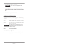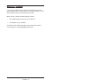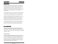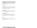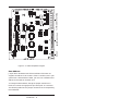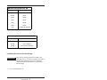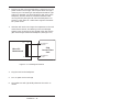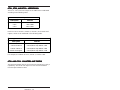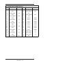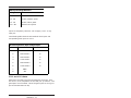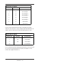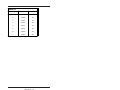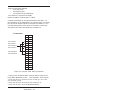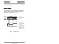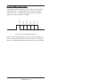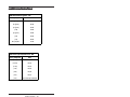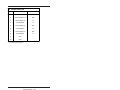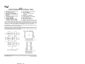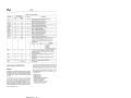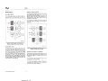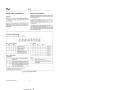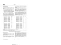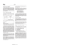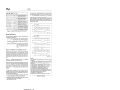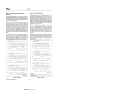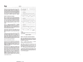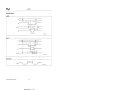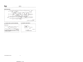
1
5300 User’s Manual Doc. #02793 Rev 0498 OCTAGON SYSTEMS CORPORATION® 6510 W. 91st Ave. Westminster, CO 80030 Tech. Support: 303–426–4521 COPYRIGHT Copyright 1990–94, 1997, 1998–Octagon Systems Corporation. All rights reserved. However, any part of this document may be reproduced, provided that Octagon Systems Corporation is cited as the source. The contents of this manual and the specifications herein may change without notice. TRADEMARKS Micro PC, PC SmartLink, Octagon Systems Corporation®, the Octagon logo and the Micro PC logo, and CAMBASIC IV are trademarks of Octagon Systems Corporation. QuickBASIC® is a registered trademark of Microsoft Corporation. Turbo C is a trademark of Borland International, Inc. NOTICE TO USER The information contained in this manual is believed to be correct. However, Octagon assumes no responsibility for any of the circuits described herein, conveys no license under any patent or other right, and makes no representations that the circuits are free from patent infringement. Octagon makes no representation or warranty that such applications will be suitable for the use specified without further testing or modification. Octagon Systems Corporation general policy does not recommend the use of its products in life support applications where the failure or malfunction of a component may directly threaten life or injury. It is a Condition of Sale that the user of Octagon products in life support applications assumes all the risk of such use and indemnifies Octagon against all damage. IMPOR TANT! IMPORT Please read before installing your product. Octagon’s products are designed to be high in performance while consuming very little power. In order to maintain this advantage, CMOS circuitry is used. CMOS chips have specific needs and some special requirements that the user must be aware of. Read the following to help avoid damage to your card from the use of CMOS chips. Using CMOS Circuitry – 1 Using CMOS Circuitry in Industrial Control Industrial computers originally used LSTTL circuits. Because many PC components are used in laptop computers, IC manufacturers are exclusively using CMOS technology. Both TTL and CMOS have failure mechanisms, but they are different. This section describes some of the common failures which are common to all manufacturers of CMOS equipment. However, much of the information has been put in the context of the Micro PC. Octagon has developed a reliable database of customer-induced, field failures. The average MTBF of Micro PC cards exceeds 11 years, yet there are failures. Most failures have been identified as customer-induced, but there is a small percentage that cannot be identified. As expected, virtually all the failures occur when bringing up the first system. On subsequent systems, the failure rate drops dramatically. ■ Approximately 20% of the returned cards are problem-free. These cards, typically, have the wrong jumper settings or the customer has problems with the software. This causes frustration for the customer and incurs a testing charge from Octagon. ■ Of the remaining 80% of the cards, 90% of these cards fail due to customer misuse and accident. Customers often cannot pinpoint the cause of the misuse. ■ Therefore, 72% of the returned cards are damaged through some type of misuse. Of the remaining 8%, Octagon is unable to determine the cause of the failure and repairs these cards at no charge if they are under warranty. The most common failures on CPU cards are over voltage of the power supply, static discharge, and damage to the serial and parallel ports. On expansion cards, the most common failures are static discharge, over voltage of inputs, over current of outputs, and misuse of the CMOS circuitry with regards to power supply sequencing. In the case of the video cards, the most common failure is to miswire the card to the flat panel display. Miswiring can damage both the card and an expensive display. ■ Multiple component failures - The chance of a random component failure is very rare since the average MTBF of an Octagon card is greater than 11 years. In a 7 year study, Using CMOS Circuitry – 2 Octagon has never found a single case where multiple IC failures were not caused by misuse or accident. It is very probable that multiple component failures indicate that they were user-induced. ■ Testing “dead” cards - For a card that is “completely nonfunctional”, there is a simple test to determine accidental over voltage, reverse voltage or other “forced” current situations. Unplug the card from the bus and remove all cables. Using an ordinary digital ohmmeter on the 2,000 ohm scale, measure the resistance between power and ground. Record this number. Reverse the ohmmeter leads and measure the resistance again. If the ratio of the resistances is 2:1 or greater, fault conditions most likely have occurred. A common cause is miswiring the power supply. ■ Improper power causes catastrophic failure - If a card has had reverse polarity or high voltage applied, replacing a failed component is not an adequate fix. Other components probably have been partially damaged or a failure mechanism has been induced. Therefore, a failure will probably occur in the future. For such cards, Octagon highly recommends that these cards be replaced. ■ Other over-voltage symptoms - In over-voltage situations, the programmable logic devices, EPROMs and CPU chips, usually fail in this order. The failed device may be hot to the touch. It is usually the case that only one IC will be overheated at a time. ■ Power sequencing - The major failure of I/O chips is caused by the external application of input voltage while the Micro PC power is off. If you apply 5V to the input of a TTL chip with the power off, nothing will happen. Applying a 5V input to a CMOS card will cause the current to flow through the input and out the 5V power pin. This current attempts to power up the card. Most inputs are rated at 25 mA maximum. When this is exceeded, the chip may be damaged. ■ Failure on power-up - Even when there is not enough current to destroy an input described above, the chip may be destroyed when the power to the card is applied. This is due to the fact that the input current biases the IC so that it acts as a forward biased diode on power-up. This type of failure is typical on serial interface chips. Using CMOS Circuitry – 3 ■ Serial and parallel - Customers sometimes connect the serial and printer devices to the Micro PC while the power is off. This can cause the failure mentioned in the above section, Failure upon power-up. Even if they are connected with the Micro PC on, there can be another failure mechanism. Some serial and printer devices do not share the same power (AC) grounding. The leakage can cause the serial or parallel signals to be 20-40V above the Micro PC ground, thus, damaging the ports as they are plugged in. This would not be a problem if the ground pin is connected first, but there is no guarantee of this. Damage to the printer port chip will cause the serial ports to fail as they share the same chip. ■ Hot insertion - Plugging cards into the card cage with the power on will usually not cause a problem. (Octagon urges that you do not do this!) However, the card may be damaged if the right sequence of pins contacts as the card is pushed into the socket. This usually damages bus driver chips and they may become hot when the power is applied. This is one of the most common failures of expansion cards. ■ Using desktop PC power supplies - Occasionally, a customer will use a regular desktop PC power supply when bringing up a system. Most of these are rated at 5V at 20A or more. Switching supplies usually require a 20% load to operate properly. This means 4A or more. Since a typical Micro PC system takes less than 2A, the supply does not regulate properly. Customers have reported that the output can drift up to 7V and/or with 7-8V voltage spikes. Unless a scope is connected, you may not see these transients. ■ Terminated backplanes - Some customers try to use Micro PC cards in backplanes that have resistor/capacitor termination networks. CMOS cards cannot be used with termination networks. Generally, the cards will function erratically or the bus drivers may fail due to excessive output currents. ■ Excessive signal lead lengths - Another source of failure that was identified years ago at Octagon was excessive lead lengths on digital inputs. Long leads act as an antenna to pick up noise. They can also act as unterminated transmission lines. When 5V is switch onto a line, it creates a transient waveform. Octagon has seen submicrosecond pulses of 8V or more. The solution is to place a capacitor, for example 0.1 µF, across the switch contact. This will also eliminate radio frequency and other high frequency pickup. Using CMOS Circuitry – 4 TABLE OF CONTENTS PREFACE ......................................................................... 1 Conventions Used In This Manual .................................................... 1 Symbols and Terminology .................................................................. 2 Technical Support ............................................................................... 3 CHAPTER 1: OVERVIEW ................................................ 5 Description .......................................................................................... 5 Major Features .................................................................................... 5 CHAPTER 2: INSTALLATION ........................................ 7 Equipment ........................................................................................... 7 Installation .......................................................................................... 7 Base Address ................................................................................ 8 Interrupt Source and Request Lines .......................................... 9 Installing the Card in the Card Cage ....................................... 10 Troubleshooting ................................................................................. 12 Power Module ............................................................................. 12 Jumper Configurations .............................................................. 12 CHAPTER 3: OPERATION ........................................... 13 Description ........................................................................................ 13 Cascading ........................................................................................... 13 CTC1, CTC2, and CTC3: Addressing ............................................. 13 CTC1 and CTC2: Counters and Timers ......................................... 14 CTC2 Optically Isolated Inputs ................................................ 16 CTC1 and CTC2 Gates .............................................................. 17 CTC3: Precision Timer .................................................................... 18 82C55A: Digital I/O ......................................................................... 18 Output Drive Capabilities ......................................................... 20 Recommended Configuration for 82C55A ................................ 20 Counter/Timer and Digital I/O Interface ........................................ 20 CHAPTER 4: APPLICATIONS ..................................... 23 Example 1: Tick Timer .................................................................... 23 Example 2: Pulse Width Modulation .............................................. 27 i APPENDIX A: COMPONENTS ..................................... 31 Schmitt Trigger ................................................................................. 31 Pulse Width Modulation ................................................................... 32 APPENDIX B: TECHNICAL DATA ............................... 33 Specifications ..................................................................................... Jumper Configurations ..................................................................... Connector Configurations ................................................................. I/O Maps ............................................................................................ 33 34 36 38 APPENDIX C: 82C54 DATA SHEET ............................ 39 WARRANTY ii PREF ACE PREFA This manual is a guide to the proper configuration and operation of your 5300 Counter/Timer Card. Installation instructions, card mapping information and jumpering options are described in the main body of the manual; the schematic and technical specifications are included in the appendices. NOTE: Additional application information is available on the Octagon Bulletin Board: Read AN–0060. (303–427–5368) The 5300 provides timing, counting, frequency measurement, frequency generation, and pulse width modulation. It is designed to be used with any Octagon Micro PC control card. This combination provides a modular system which is easy to set up, modify and use. You can also use your 5300 in conjunction with other Micro PC expansion cards, allowing you to tailor your system for a wide variety of applications. CONVENTIONS USED IN THIS MANUAL 1. Information which appears on your screen (output from your system or commands or data that you key in) is shown in a different type face. Example 1: Octagon 5066 ROM BIOS Vers X.XX Copyright (c) 1998, Octagon Systems, Corp. All Rights Reserved Example 2: Press the <ESC> key. 2. Italicized refers to information that is specific to your particular system or program, for example, Enter filename means enter the name of your file. Names of other sections or manuals are also italicized. Preface – 1 3. Warnings always appear in this format: WARNING: The warning message appears here. 4. Paired angle brackets are used to indicate a specific key on your keyboard, for example, <ESC> means the escape key; <CTRL> means the control key; <F1> means the F1 function key. 5. All addresses are given in hexadecimal. SYMBOLS AND TERMINOLOGY Throughout this manual, the following symbols and terminology are used: W[ – ] Denotes a jumper block and the pins to connect. NOTE Information under this heading presents helpful tips for using the 5300. WARNING: WARNING: PWM Information under this heading warns you of situations which might cause catastrophic or irreversible damage. Pulse Width Modulation. TTL Compatible 0–5V logic levels. H The suffix “H” denotes a hexadecimal number. For example, 1000H in hexadecimal equals 4096 in decimal. Preface – 2 TECHNICAL SUPPORT If you have a question about the 5300 Counter/Timer Card and can’t find the answer in this manual, call Technical Support. They will be ready to give you the assistance you need. When you call, please have the following at hand: • Your 5300 Counter/Timer Card User’s Manual • A description of your problem The direct line to Technical Support is 303–426–4521 and the e–mail address is [email protected]. Preface – 3 This page intentionally left blank. Preface – 4 CHAPTER 1 OVER VIEW VERVIEW DESCRIPTION The 5300 Counter/Timer I/O Card provides timing, counting, frequency measurement, frequency generation, and pulse width modulation (PWM). The 5300 can be used for precision timing, speed measurement, event counting, and related tasks. For example, you can use the 5300 to control pick and place machines; to measure and adjust motor speed; or to count objects on a conveyor belt. The 5300 measures 4.5 in. x 4.9 in. and uses one slot of the Micro PC card cage. It is compatible with all Micro PC Control Cards. You can use as many cards as space in the card cage will allow. The 5300 uses three 82C54 chips for counting and timing. An 82C55 chip provides eight general–purpose digital I/O lines. The 5300 has two programmable time bases, six counters and six counter/timer inputs. Three of the counter inputs are optically isolated for greater safety and less interference from noise. The counter/timers operate at 5V (TTL) levels with signal conditioning to minimize noise. They have gate inputs and counter outputs. All clock inputs go through Schmitt trigger buffers. MAJOR FEATURES Time Base 0 of the two programmable time bases is an 8 MHz source with a 16–bit divider. It can generate frequencies from 122 Hz to 4 MHz. The other time base has an 8 MHz source and is cascaded to create a 32–bit divider. Output frequencies range from 0.0005 Hz to 2 MHz. Counter/Timers The six counter/timer sections have clock, gate, and output leads available. Different modes of operation are possible by using various clock configurations. The lines are terminated in 10– and 34–pin IDC connectors. Every other lead is ground, which minimizes the chance of cross coupling and noise. The count inputs have signal conditioners to minimize noise effects. These inputs and the gate inputs have pull–up resistors. Overview – 5 Digital I/O The 5300 has eight digital I/O lines that can be used for general purpose control and input. The lines can be programmed as inputs or outputs in groups of four. Interrupts A jumper determines whether the output of a counter or one of the digital I/O lines is the interrupt source. The jumper can also be configured so that there is no interrupt source. The selected source can be jumpered to IRQ2 through IRQ7. Access Indicator An LED indicator flashes briefly whenever the 5300 is accessed. This is useful when troubleshooting the card to know if a communications link has been established. Opto–isolated inputs Three counter inputs are optically isolated and terminated in a screw terminal block. The isolation between channels and ground is 2500V. However, for operator safety, no more than 32V should be applied. Counters The maximum count rate input is 1 MHz. The input range is 4 to 12 volts but can be increased up to 48V when used in conjunction with an external resistor. Overview – 6 CHAPTER 2 INST ALLA TION INSTALLA ALLATION This chapter includes information on setting the base address, selecting the interrupt request line, and installing the 5300 in the Micro PC card cage. Refer to the Operation chapter for more information. The 5300 Counter/Timer I/O Card uses one slot of the Micro PC card cage. It may be used with any Micro PC Control Card. You can use as many cards as space in the card cage will allow. WARNING: The 5300 contains static sensitive CMOS components. The greatest danger occurs when the card is plugged into a card cage. The 5300 becomes charged by the user and the static discharges to the backplane from the pin closest to the card connector. If that pin happens to be an input pin, even TTL inputs may be damaged. To avoid damaging your card and its components: 1. Ground yourself before handling the 5300 Counter/Timer Card. 2. Disconnect power before removing or inserting the 5300 Card. EQUIPMENT You will need the following equipment (or equivalent) to use your 5300. • • • • • 5300 Counter/Timer Card Micro PC Control Card Micro PC Card Cage Power Supply or Module Software appropriate for your system INSTALLATION Before installing the 5300, refer to Figure 2.1 for the location of various connectors and jumpers. Installation – 7 Optically isolated inputs CTC and digital I/O Address jumper Interrupt selection jumper CTC I/O Figure 2–1—5300 Component Diagram Base Address Jumper block W1 determines the base address of the 5300. As shipped, the address is set to 100H. If there is another card in your system with a base address of 100H, you must use a different base address for the 5300 or the other card. To change the base address, change the jumper connections in block W1. Connect the appropriate pins with push–on connectors. The following table lists the jumper connections and corresponding base addresses. Installation – 8 5300 Base Address Select: W1 Pins Jumpered Base I/O Address [1-2][3-4][5-6] 100H* [3-4][5-6] 110H [1-2][5-6] 120H [5-6] 130H [1-2][3-4] 140H [3-4] 150H [1-2] 160H No jumpers 170H * = default INTERRUPT SOURCE & INTERRUPT REQUEST LINES As shipped, the card does not have any interrupt lines selected. In this configuration, the pins in jumper block W2 are jumpered for no interrupts. The following tables list the jumper configurations and corresponding interrupt request lines and sources. Connect appropriate pins with push–on connectors. There are two possible interrupt sources on the 5300: The CTC 2 Output 0 signal, or the PIO 0 digital signal when configured as an output. You can choose either signal as a source, but you can not use both signals at the same time. Select the desired interrupt source via jumper block W2. There are six interrupt request lines, IRQ2 through IRQ 7, which go to the bus. Pins 1 through 12 of jumper block W2 select the interrupt request line; pins 13–16 select the interrupt source. You will need to write your own interrupt handler for either interrupt source. Refer to Example 1 programming example in the Applications chapter. Installation – 9 5300 Interrupt Request Lines: W2 Pins Jumpered IRQ [1-2] IRQ2 [11-12] IRQ3 [9-10] IRQ4 [7-8] IRQ5 [5-6] IRQ6 [3-4] IRQ7 [1-3] No interrupt selected* * = default 5300 Interrupt Sources: W2 Pins Jumpered Base I/O Address [13-14] PIO 0 Output [15-16] CTC2 Output 0 [14-16] No interrupt selected* * = default Installing the Card in the Card Cage WARNING: 1. Take care to correctly position the 5300 in the card cage. The VCC and ground signals must match those on the backplane. Figure 2–2 shows the relative position of the 5300 as it is installed in the card cage. Turn card cage power off. Installation – 10 2. Position the cage so that the backplane is away from you, the power module is to the right, and the open side of the cage is closest to you. The lettering on the backplane should be right side up (for example, you should be able to read “A31” on the backplane), with the words OCTAGON SYSTEMS CORP. running vertically along the left side of the backplane. This position is “feet down” for a table mount cage and “feet back” for a panel mount. 3. Slide the card into the card cage. The components on the card should face to the left. The lettering on the card (Octagon Systems Corp.) should be on the top edge of the card and the gold contact fingers toward the backplane. (See Figure 2–2) A31 B31 Card Edge Pins A31 & B31 5300 Counter/Timer Card Micro-PC Motherboard A1 B1 Card Edge Pins A1 & B1 Figure 2–2—Card Edge Orientation 4. Plug the card into the backplane. 5. Turn on power to the card cage. 6. The amber LED will light briefly whenever the card is accessed. Installation – 11 TROUBLESHOOTING If you have trouble getting your system to work properly, remove all cards except the Control Card and the 5300 card from your system. Check the power module and jumpers. If you still encounter difficulties, please contact Technical Support at either the telephone number, 303–426–4521, or the e–mail address, [email protected]. Power Module Make sure the power cord is properly connected between the power module and the power source. Make sure the Control Card and 5300 are receiving power. The power module voltage should be in the 5 to +/–0.25V range when measured at the connector pins. The power module ripple should be less than 50 mV. Jumper Configurations The 5300 is shipped with jumper connections in place for Base I/O Address 100H and no interrupts selected. Jumper changes are usually not needed to get the system running. If you changed the jumpers and the system is not working properly, return the system to the original jumper positions. If the system still does not work, contact Technical Support. Installation – 12 CHAPTER 3 OPERA TION OPERATION DESCRIPTION The 5300 Counter/Timer Card has three 82C54 counter/timer chips. Each chip has three counters/timers. CTC1 is a general purpose counter/timer; CTC2 has optically isolated clock inputs; CTC3 can be used as a timer only. All counter/timer I/O lines go to J1 and J2. You can use a UTB–34 to connect external wiring to J1. You can also use an STB–10 to connect external wiring to J2. The clock inputs on CTC1 and J1 are buffered with a Schmitt trigger. The clock inputs on CTC2 come from either the optical isolator and terminal block or directly from J1 (without optical isolation). The 82C54 counters are all programmable. Generally, you will program the mode (which is the function) and the number of counts which must occur (the variable). For example, you might specify that a certain number of counts must occur before a pulse is generated. CASCADING Each counter can count from 0 to 65,535. If you need to count to a higher number, you will need to cascade the counters—connect them so that the count output from one counter goes to the next counter clock input. Connections to allow cascading must be done externally to the card through J1 and J2. For example, if you need to count to 150,000, physically wire the output from one counter to the clock input of another counter. One way to do this is to connect pin 17 to pin 7 via the UTB–34, which will send the output from counter 2 to counter 1 input on CTC1. Operation – 13 CTC1, CTC2, AND CTC3: ADDRESSING The CTC1, CTC2, and CTC3 chips on the 5300 card are addressed according to the following table: 5300 Counter/Timer Chip Addresses Description Address CTC1 Base + 04H CTC2 Base + 08H CTC3 Base + 0CH Each CTC has a counter 0, counter 1, counter 2, and control word register, which are all addressed in the following table: 8254 Register Addresses Description Address Counter channel 0 Counter/timer chip address + 00H Counter channel 1 Counter/timer chip address + 01H Counter channel 2 Counter/timer chip address + 02H Control word register Counter/timer chip address + 03H For example, the address of CTC1, counter 2, is Base + 06H. CTC1 AND CTC2: COUNTERS AND TIMERS The input and output lines of CTC1 and CTC2 connect to J1 and J2 respectively. The three clock inputs of CTC2 are also available from the opto isolators at TB1. Operation – 14 J1: Counter/Timer & Digital I/O Port Pin# Function Direction Pin# Function 1 CTC1 Clock 0 In 18 Gnd 2 Gnd 19 CTC3 Output 0 3 CTC1 Gate 0 20 Gnd 4 Gnd 21 CTC3 Output 2 5 CTC1 Output 0 22 Gnd 6 Gnd 23 PIO 0 In/Out 7 CTC1 Clock 1 24 PIO 1 In/Out 8 Gnd 25 PIO 2 In/Out 9 CTC1 Gate 1 10 Gnd 11 CTC1 Output 1 12 Gnd 13 CTC1 Clock 2 14 Gnd 15 CTC1 Gate 2 16 Gnd 17 CTC1 Output 2 In Out In In Out In In Out Direction Out Out 26 PIO 3 In/Out 27 PIO 4 In/Out 28 PIO 5 In/Out 29 PIO 6 In/Out 30 PIO 7 In/Out 31 CTC2 Clock 2 In 32 CTC2 Clock 1 In 33 CTC2 Clock 0 In 34 +5V Operation – 15 J2: Counter/Timer Port Pin# Function Direction 1 CTC3 Output 2 / 2* Out 2 CTC3 Output 2 / 2 Out 3 CTC2 Output 0 In 4 CTC2 Gate 0 In 5 CTC2 Output 1 Out 6 CTC2 Gate 1 In 7 CTC2 Output 2 Out 8 CTC2 Gate 2 In 9 Gnd 10 Gnd * = Inverted output of pin 2. CTC2 Optically Isolated Inputs The optical isolator inputs are available at TB1 and go to the clock inputs on CTC2. You can bypass the isolation by connecting directly to J1. Use the opto isolators if your environment (plant wiring, for instance) could generate spurious ground loops or differences in potential. Opto isolators are often used for switch inputs and magnetic pick–ups in electrically noisy conditions, or for anything that needs to be electrically isolated. The isolation voltage is 48V. Opto isolator inputs require 4 to 12 volts to trigger the clock. You can use higher voltages provided that you limit the current to 15 mA by placing a resistor in series with the input. The following table shows which resistor to use with different voltage levels. Operation – 16 5300 Input Voltage Resistors Voltage Resistor 4.0V - 12V No resistor 5.2V - 16V 150 ohms, 0.125W or greater 7.4V - 24V 430 ohms, 0.5W or greater 14.2V - 48V 1300 ohms, 2W or greater Inputs are not polarity sensitive. You can apply + and – to any input pair. The following table shows the TB1 terminal block inputs and corresponding clock inputs on CTC2. TB1: Terminal Block, Opto–Isolated Inputs Pin# Function Direction 1 –CTC2 Clock 2 In 2 +CTC2 Clock 2 In 3 +CTC2 Clock 1 In 4 –CTC2 Clock 1 In 5 +CTC2 Clock 0 In 6 –CTC2 Clock 0 In 7 GND 8 +5V CTC1 and CTC2 Gates Gate inputs are used to turn the counter/timer on and off. They are all TTL (0–5V) compatible; all have 10K pull–up resistors. The gate inputs are not isolated. Two of the gate inputs on CTC1 go to port A of the 82C55A PIO chip. Operation – 17 CTC3: PRECISION TIMER CTC3 is configured as a programmable precision timer. The 8 MHz crystal oscillator provides high resolution, so you can precisely time events. CTC3 has two output lines which connect to J1; no other counter lines are available. Although it is used exclusively as a timer, you must still specify the counter mode. Two of the counters in CTC3 are cascadable, so you can get longer (i.e., lower frequency) time periods. For example, you can create a large frequency divider by connecting the output from CTC3 Output 0 (pin 19 on J1) to CTC1 Clock 0 (pin 1 on J1). This is useful for PWM output and can result in high resolution even at very low frequencies. Precision with this system can be as fine as 0.1%. Since the time interval can be programmed very precisely, you can create a finely–tuned PWM output. For example, instead of specifying that the pulse be on for 1 mS and off for 9 mS, you can specify that it be on for .01 mS and off for .09 mS—maintaining the same ratio but achieving a much finer resolution. You can also configure CTC2 Output 0 as the interrupt source. Connect the output of CTC3 Output 0 (pin 19 on J1) to CTC2 Clock 0 (pin 33 on J1). The output from CTC2 Output 0 goes to jumper block W2, which determines the interrupt select line (IRQ2 – IRQ7). Using your interrupt handler, you can process precisely timed interrupts. Refer to example 1 in the Applications chapter. 82C55A: DIGITAL I/O 82C55A general purpose, digital input/output IC. It has three 8–bit ports and a control port which is addressed according to the following table: Operation – 18 5300 Port Addresses Description Address Port A Base + 00H Port B Base + 01H Port C Base + 02H Control Register Base + 03H On power–up or reset, all three ports are in the input state. This configuration will not cause any operational problems or interference with the counters. You can alter which ports are inputs or outputs by writing a control command to the control register in the 82C55A. The examples below assume the base address is 100H. The following table lists the control commands for the different input/output possibilities. 5300 I/O Control Register Commands HEX DEC Port A* Port B* Upper Port C* Lower Port C* 90H 144 IN OUT OUT OUT 91H 145 IN OUT OUT IN 92H 146 IN IN OUT OUT 93H 147 IN IN OUT IN 98H 152 IN OUT IN OUT 99H 153 IN OUT IN IN 9AH 154 IN IN IN OUT 9BH 155 IN IN IN IN *Port A must be an input. Port B can be inputs or outputs. Each half of Port C is programmable. Port C may be either inputs or outputs. Upper C includes bits 4 through 7 and Lower C includes bits 0 through 3. For example, if you want ports B and C to be outputs while retaining port A as inputs, use: Operation – 19 OUT 103H,90H Port B will now output all “1”s after: OUT 101H,FFH or all “0”s after: OUT 101H,0 Output Drive Capabilities The output drive capacity of the 82C55A is one TTL load. Any output on port A, B, or C can sink or source 2.5 mA. Recommended Configuration for 82C55A Port A: Port B: Port C: all inputs all inputs unless you intend to control all the gates on CTC2 inputs, outputs, or both. NOTE: Port A must be set as inputs. COUNTER/TIMER AND DIGITAL I/O INTERFACE The 24 programmable I/O lines of 82C55A are divided into three addressable ports of 8 bits each plus one port which contains the control register. The control register is used to determine the configuration of the 24 lines. Refer to the Control Register command table in this chapter. All outputs from CTC1 and CTC2 go to port A of the 82C55A. Port A must be programmed as an input. Operation – 20 5300 Port A Line Signals Port A Line Direction Counter/Timer 0 In CTC1 Output 0 1 In CTC1 Output 1 2 In CTC1 Output 2 3 In CTC2 Output 0 4 In CTC2 Output 1 5 In CTC2 Output 2 6 In CTC1 Gate 0 7 In CTC1 Gate 1 Ports A and B of 82C55A can be used to read gate and output status on CTC1 and CTC2. If you configure port B of 82C55A as an output, you can use Port B to control the gate inputs on CTC2. 5300 Port B Line Signals Port B Line Direction Counter/Timer 0 Out CTC2 Gate 0 1 Out CTC2 Gate 1 2 Out CTC2 Gate 2 3-7 No Connection Port C of 82C55A provides eight general purpose I/O lines which go to J1 and can be programmed as all inputs, all outputs, or four lines of each (upper and lower C). Operation – 21 5300 Port C Port C Line Direction J1 Pin # 0 In/Out 23 1 In/Out 24 2 In/Out 25 3 In/Out 26 4 In/Out 27 5 In/Out 28 6 In/Out 29 7 In/Out 30 Operation – 22 Chapter 4 APPLICA TIONS APPLICATIONS EXAMPLE 1: TICK TIMER You can also configure CTC2 Output 0 as the interrupt source. Connect the output of CTC3 Output 0 (pin 19 on J1) to CTC2 Clock 0 (pin 33 on J1). The output from CTC2 Output 0 goes to jumper block W2, which determines the interrupt select line (IRQ2 – IRQ7). Using your interrupt handler, you can process precisely timed interrupts. The following example is a demonstration program which sets up the 5300 to produce a 100 Hz tick timer. NOTE: The hard disk interrupt is used for this demo. If you are using a hard disk, you must change the interrupt to another number. NOTE: Additional application information is available on the Octagon Bulletin Board: Read AN–0060 (303–427–5368) /* Filename: 5300tick.c Function name: 5300tick Edit date: 10/29/90 Function: Demonstration program setting up the 5300 to produce a 100 Hz tick timer. NOTE: The hard disk interrupt is used for this demo. If you are using a hard disk, you must change the interrupt to another number. Compiled using Borland's Turbo–C, version 2.0. Settings for the 5300: Connect J1–19 to J1–33. Set jumpers W2[15–16] and W2[7–8] to enable interrupts Revisions: */ Applications – 23 /* Includes */ #include #include #include "stdio.h" "dos.h" "time.h" /* Definitions */ /* set up base address of 5300 */ #define BASE_5300 0x100 /* define offset addresses of components*/ #define PIO_5300 0 + BASE_5300 /* counter/timers 1 through 3 */ #define CTC1 4+BASE_5300 #define CTC2 8+BASE_5300 #define CTC3 12+BASE_5300 /* Declarations */ /* counter for interrupt int irqcnt; /* interrupt number int */ */ itrnum = 0x0d; /* pointer to old interrupt */ void interrupt (*oldint)(); /* flag for interrupt routine to stop initializing the tick counter */ int notick; /* Program */ /* interrupt handler */ /* This is the program that processes the interrupt. It must go before main when using Turbo–C and Quick–C. */ Applications – 24 void interrupt tick() { /* This example uses IRQ5 which is the hard disk interrupt. If you are using a hard disk, you may want to use another unused IRQ port. */ /* Check to see if we should continue to process this interrupt. If not, simply exit */ if (notick == 0) { /* send count to port C output, line 0 on the 5300. This output should toggle at a 50 Hz rate */ outportb(PIO_5300+2,irqcnt); /* reset counter to 0 if overflow irqcnt++; */ if(irqcnt == 256) irqcnt = 0; /* re–initialize counter outportb(CTC2,232); */ outportb(CTC2,3); /* reset interrupt port */ outportb(0x20,0x20); } } main() { /* use the hard disk interrupt IRQ5 (0DH) transfer control on each tick. */ /* get & save old interrupt vector */ oldint = getvect(itrnum); /* set interrupts setvect(itrnum,tick); /* set 5300 for 100 times/second Applications – 25 */ */ /* set CTC3O0 to mode 2 ( rate generator) and to divide by 80 */ outportb(CTC3+3,0x34); /* Divide by 80. outportb(CTC3,80); LSB first, then MSB */ outportb(CTC3,0); /* set CTC2O0 for mode 4 (triggered strobe) and to divide by 1000 (3 * 256 + 232 = 1000) */ outportb(CTC2+3,0x38); outportb(CTC2,3); outportb(CTC2,232); /* set up 82C55A port on 5300 for A & B as inputs, C as outputs */ outportb(PIO_5300+3,0x92); /* set up for interrupts */ outportb(0x21,0x98); /* main program loop. This example simply waits for a key press. Your program would continue. */ /* check for a keyboard hit. program */ If one, then exit puts("Waiting for keyboard hit.\n"); while (kbhit() == 0) ; /* tell the interrupt handler not to reset the timer and get the character */ notick = 1; getch(); /* restore interrupt handler setvect(itrnum,oldint); } Applications – 26 */ EXAMPLE 2: PULSE WIDTH MODULATION This program uses 3 of the 9 counter/timers on the 5300 card to generate a pulse width modulated output. The first stage, CTC3 Counter 3, is used as a simple ‘divide by 8’ counter in the ‘SQUARE WAVE’ mode. This produces a 1 MHz square wave output that is used as the CLOCK input for the other two stages. The second stage, CTC 1 Counter 2, determines the output frequency. The third stage, CTC1 Counter 1, is used in the One Shot mode providing the modulating element. In the QuickBASIC example program, the following variables are used: • FR = Requested frequency FR is the frequency to be modulated. This frequency has a maximum and minimum value. FR can be any frequency multiple of 1 MHz that is in the range of 16 Hz to 500 KHz. • FD = Frequency Divisor for the requested frequency FD is a value calculated in the program that is an integer in the range of 2 to 65,535. • DU = Requested Duty cycle (that the output signal is true) DU represents the Duty Cycle in percent. The time that the output signal is ON verses the total available time, defines the duty cycle. • DX = Decimal equivalent for duty cycle DX is calculated in the program and is based on the input ‘DU’. • PD = Pulse width Divisor. PD is a value calculated by the program that is an integer in the range of 2 to 65,535. Applications – 27 Note the relationship between: • the 1 MHz clock, • the frequency and • the resolution of the modulation. The resolution is expressed as follows: RESOLUTION(%) = FREQUENCY / 1 MHz A 100 KHz frequency can only be modulated in 10% steps. A 1 KHz frequency can be modulated in 0.1% percent steps. The lower the value of the output frequency the higher the resolution. Also, note that the frequency of the output is rounded to a value that will equal 1 MHz when multiplied by the integer ‘FD’. J1 connector 1 2 3 4 5 6 CTC1 Clock 1 7 8 CTC1 Gate 1 9 10 CTC1 Output 1 11 12 CTC1 Clock 2 13 14 15 16 CTC1 Output 2 17 18 CTC3 Output 0 19 20 21 22 23 24 25 26 27 28 29 30 31 32 33 34 Figure 4–1—Counter Timer Wiring Connection ' These are the connections which must be made in order for the Pulse Width Modulator to work. The connections are as follows: ' CTC3 Ch0 'OUT' (J1-19) to CTC1 Ch1 'CLOCK' (J1-7) & CTC1 Ch2 'CLOCK' (J1-13) ' CTC1 Ch2 'OUT' (J1-17) to CTC1 Ch1 'GATE' (J1-9) ' CTC1 Ch1 'OUT' (J1-11) is the Modulated Signal' Applications – 28 'OPTION BASE 1 ' Pulse Width Modulation Example using Quick Basic ' Base Address of 5300 card configured to 100 Hex ADDBASE = &H100 CTC1 = ADDBASE + 4 CTC2 = ADDBASE + 8 CTC3 = ADDBASE + 12 ' Divide on board Master clock by 4. 8 MHz divided by 4 equals 2 MHz ' Set CTC3, Ch0 to mode 3 OUT CTC3 + 3, &H36 OUT CTC3 + 0, 8 OUT CTC3 + 0, 0 ' Get Frequency from user INPUT "Enter the frequency in 'Hz'"; FR INPUT “Enter the Duty Cycle in ‘%’”; DU ' Calculate the divisor for the 82C54 for correct frequency generation FD = 1000000! / FR ' CTC1 Ch 2, set to Mode 3 OUT CTC1 + 3, &HB6 ' Calculate low and high byte counts LSB MSB OUT OUT = FD MOD 256 = INT(FD / 256) CTC1 + 2, LSB CTC1 + 2, MSB ' Calculate duty cycle in number of clock counts DX = 1 - DU / 100 PD = FD * DX LSB = PD MOD 256 MSB = INT(PD / 256) Applications – 29 ' Set CTC1, CH1 to Mode 1 OUT CTC1 + 3, &H72 OUT CTC1 + 1, LSB OUT CTC1 + 1, MSB END Applications – 30 APPENDIX A COMPONENTS This appendix includes some basic information on Schmitt triggers and pulse width modulation. SCHMITT TRIGGER A Schmitt trigger provides better noise immunity than a TTL input. The output will turn on when the signal reaches VT+ but will not turn off until the signal drops below VT–. With TTL, the signal could be on or off between VT– and VT+. Received signal from transmission line with thresholds at different amplitudes. VT+ Signal Amplitude VTH VT Recovered signal with CMOS Schmitt trigger, VT+ and VT. Restores true waveform. 1 Level 0 Level 0 1 2 3 4 5 6 7 8 9 10 TIME (µS) Recovered signal from Schmitt is same width as comparator with threshold at VTH, and is only delayed in time. Figure A–1—Schmitt Trigger Components – 31 PULSE WIDTH MODULATION 75% 67.5% 50% 37.5% 25% 12.5% Pulse width modulation (PWM) is often used in controlling motor speed, light levels, or damper opening. The width of the pulse— how long it is on—is modulated according to the level needed. Figure A–2 shows a general–case PWM. Figure A–2—Pulse Width Modulation Within a given (programmed) time interval, the pulse signal may be on for less than 100% of the time. How long it is on—the pulse width —is determined by the amount of “ON” you want to achieve. Components – 32 APPENDIX B TECHNICAL D ATA DA SPECIFICATIONS Power Specifications 5V at 50 mA typical Environmental Specifications –40° to 85° C operating RH 5% to 95%, noncondensing Clock Input 8 MHz max. Optically Isolated Input Rate 1 MHz max. Optically Isolated Input Current 15 mA max., 5 mA min. Digital I/O 8 lines, programmable as 4 or 8 inputs or outputs. TTL compatible logic. Size 4.5 in. x 4.9 in. For additional information, please turn to Appendix C, which includes the data sheet for the 82C54 Counter/Timer chip. Technical Data – 33 JUMPER CONFIGURATIONS 5300 Base Address Select: W1 Pins Jumpered Base I/O Address [1-2][3-4][5-6] 100H* [3-4][5-6] 110H [1-2][5-6] 120H [5-6] 130H [1-2][3-4] 140H [3-4] 150H [1-2] 160H No jumpers 170H * = default 5300 Interrupt Request Lines: W2 Pins Jumpered IRQ [1-2] IRQ2 [11-12] IRQ3 [9-10] IRQ4 [7-8] IRQ5 [5-6] IRQ6 [3-4] IRQ7 [1-3] No interrupt selected* * = default Technical Data – 34 5300 Interrupt Sources: W2 Pins Jumpered Base I/O Address [13-14] PIO 0 Output [15-16] CTC2 Output 0 [14-16] No interrupt selected* * = default CONNECTOR CONFIGURATIONS J1: Counter/Timer & Digital I/O Port Pin# Function Direction Pin# Function 1 CTC1 Clock 0 In 18 Gnd 19 CTC3 Output 0 In 20 Gnd 21 CTC3 Output 2 22 Gnd 23 PIO 0 In/Out 24 PIO 1 In/Out 25 PIO 2 In/Out 26 PIO 3 In/Out 27 PIO 4 In/Out 28 PIO 5 In/Out 29 PIO 6 In/Out 30 PIO 7 In/Out 31 CTC2 Clock 2 In 32 CTC2 Clock 1 In 33 CTC2 Clock 0 In 34 +5V 2 Gnd 3 CTC1 Gate 0 4 Gnd 5 CTC1 Output 0 6 Gnd 7 CTC1 Clock 1 8 Gnd 9 CTC1 Gate 1 10 Gnd 11 CTC1 Output 1 12 Gnd 13 CTC1 Clock 2 14 Gnd 15 CTC1 Gate 2 16 Gnd 17 CTC1 Output 2 Out In In Out In In Out Technical Data – 35 Direction Out Out J2: Counter/Timer Port Pin# Function Direction 1 CTC3 Output 2 / 2* Out 2 CTC3 Output 2 / 2 Out 3 CTC2 Output 0 In 4 CTC2 Gate 0 In 5 CTC2 Output 1 Out 6 CTC2 Gate 1 In 7 CTC2 Output 2 Out 8 CTC2 Gate 2 In 9 Gnd 10 Gnd * = Inverted output of pin 2. Technical Data – 36 I/O MAPS 5300 I/O Map 82C55A Digital I/O Chip Description Address Port A Base + 0x00 Port B Base + 0x01 Port C Base + 0x02 Control Base + 0x03 8254 CTC1 Description Address Counter 0 Base + 0x04 Counter 1 Base + 0x05 Counter 2 Base + 0x06 Control CTC1 Base + 0x07 8254 CTC2 Description Address Counter 0 Base + 0x08 Counter 1 Base + 0x09 Counter 2 Base + 0x0A Control CTC2 Base + 0x0B 8254 CTC3 Description Address Counter 0 Base + 0x0C Counter 1 Base + 0x0D Counter 2 Base + 0x0E Control CTC3 Base + 0x0F Technical Data – 37 This page intentionally left blank. Technical Data – 38 APPENDIX C 82C54 D ATA SHEET DA CHMOS PROGRAMMABLE INTERVAL TIMER The material in this appendix is copyright 1989, Intel Corporation. Appendix C – 39 Appendix C – 40 Appendix C – 41 Appendix C – 42 Appendix C – 43 Appendix C – 44 Appendix C – 45 Appendix C – 46 Appendix C – 47 Appendix C – 48 Appendix C – 49 Appendix C – 50 Appendix C – 51 Appendix C – 52 Appendix C – 53 Appendix C – 54 Appendix C – 55 Appendix C – 56 WARRANTY Octagon Systems Corporation (Octagon), warrants that its standard hardware products will be free from defects in materials and workmanship under normal use and service for the current established warranty period. Octagon’s obligation under this warranty shall not arise until Buyer returns the defective product, freight prepaid to Octagon’s facility or another specified location. Octagon’s only responsibility under this warranty is, at its option, to replace or repair, free of charge, any defective component part of such products. LIMITATIONS ON WARRANTY The warranty set forth above does not extend to and shall not apply to: 1. 2. 3. Products, including software, which have been repaired or altered by other than Octagon personnel, unless Buyer has properly altered or repaired the products in accordance with procedures previously approved in writing by Octagon. Products which have been subject to power supply reversal, misuse, neglect, accident, or improper installation. The design, capability, capacity, or suitability for use of the Software. Software is licensed on an “AS IS” basis without warranty. The warranty and remedies set forth above are in lieu of all other warranties expressed or implied, oral or written, either in fact or by operation of law, statutory or otherwise, including warranties of merchantability and fitness for a particular purpose, which Octagon specifically disclaims. Octagon neither assumes nor authorizes any other liability in connection with the sale, installation or use of its products. Octagon shall have no liability for incidental or consequential damages of any kind arising out of the sale, delay in delivery, installation, or use of its products. SERVICE POLICY 1. 2. 3. Octagon’s goal is to ship your product within 5 working days of receipt. If a product should fail during the warranty period, it will be repaired free of charge. For out of warranty repairs, the customer will be invoiced for repair charges at current standard labor and materials rates. Customers that return products for repairs, within the warranty period, and the product is found to be free of defect, may be liable for the minimum current repair charge. RETURNING A PRODUCT FOR REPAIR Upon determining that repair services are required, the customer must: 1. 2. 3. 4. 5. 6. 7. Obtain an RMA (Return Material Authorization) number from the Customer Service Department, 303-430–1500. If the request is for an out of warranty repair, a purchase order number or other acceptable information must be supplied by the customer. Include a list of problems encountered along with your name, address, telephone, and RMA number. Carefully package the product in an antistatic bag. (Failure to package in antistatic material will VOID all warranties.) Then package in a safe container for shipping. Write RMA number on the outside of the box. For products under warranty, the customer pays for shipping to Octagon. Octagon pays for shipping back to customer. Other conditions and limitations may apply to international shipments. NOTE: PRODUCTS RETURNED TO OCTAGON FREIGHT COLLECT OR WITHOUT AN RMA NUMBER CANNOT BE ACCEPTED AND WILL BE RETURNED FREIGHT COLLECT. RETURNS There will be a 15% restocking charge on returned product that is unopened and unused, if Octagon accepts such a return. Returns will not be accepted 30 days after purchase. Opened and/or used products, non-standard products, software and printed materials are not returnable without prior written agreement. GOVERNING LAW This agreement is made in, governed by and shall be construed in accordance with the laws of the State of Colorado. The information in this manual is provided for reference only. Octagon does not assume any liability arising out of the application or use of the information or products described in this manual. This manual may contain or reference information and products protected by copyrights or patents. No license is conveyed under the rights of Octagon or others.