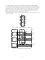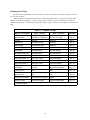
1
DM6210 Users Manual RTD Embedded Technologies Inc. (Real Time Devices) ISO9001 and AS9100 Certified Accessing the Analog World® BDM-610010009 Rev. A DM6210 Users Manual RTD Embedded Technologies, INC. 103 Innovation Blvd. State College, PA 16803-0906 Phone: +1-814-234-8087 FAX: +1-814-234-5218 E-mail [email protected] [email protected] web site http://www.rtd.com Revision History Rev. A New manual naming method Published by: RTD Embedded Technologies, Inc. 103 Innovation Blvd. State College, PA 16803-0906 Copyright 1999, 2002, 2003 by RTD Embedded Technologies, Inc. All rights reserved Printed in U.S.A. The RTD Logo is a registered trademark of RTD Embedded Technologies. cpuModule and utilityModule are trademarks of RTD Embedded Technologies. PhoenixPICO and PheonixPICO BIOS are trademarks of Phoenix Technologies Ltd. PS/ 2, PC/XT, PC/AT and IBM are trademarks of International Business Machines Inc. MS-DOS, Windows, Windows 95, Windows 98 and Windows NT are trademarks of Microsoft Corp. PC/104 is a registered trademark of PC/104 Consortium. All other trademarks appearing in this document are the property of their respective owners. Table of Contents INTRODUCTION .................................................................................................................................... i-1 Analog-to-Digital Conversion ..............................................................................................................................i-3 8254 Timer/Counter .............................................................................................................................................. i-3 Digital I/O ............................................................................................................................................................... i-3 What Comes With Your Module ..........................................................................................................................i-3 Module Accessories .............................................................................................................................................. i-4 Hardware Accessories ....................................................................................................................................... i-4 Optional Configurations ....................................................................................................................................... i-4 Using This Manual ................................................................................................................................................i-4 When You Need Help ............................................................................................................................................i-4 CHAPTER 1 MODULE SETTINGS ............................................................................................... 1-1 Factory-Configured Switch and Jumper Settings .............................................................................................. 1-3 JP1 8254 Timer/Counter Clock Sources (Factory Settings: CLK0-OSC, CLK1-OT0, CLK2-OT1) .... 1-4 P5 Analog Input Voltage Range (Factory Setting: 10V) ........................................................................1-5 P6 Analog Input Voltage Polarity (Factory Setting: BIP (Bipolar)) ...................................................... 1-5 S1 Base Address (Factory Setting: 300 hex (768 decimal)) .................................................................... 1 -6 JS3, JS4, JS5 and JS6, Pull-up/Pull-down Resistors on Digital I/O Lines ....................................................... 1-7 Gx, Resistor Configurable Gain .......................................................................................................................... 1-8 CHAPTER 2 MODULE INSTALLATION ..................................................................................... 2-1 Module Installation .............................................................................................................................................. 2-3 External I/O Connections ..................................................................................................................................... 2-4 Connecting the Analog Inputs ........................................................................................................................ 2-4 Connecting the Timer/Counters and Digital I/O ............................................................................................ 2-4 Running the 6210DIAG Diagnostics Program ................................................................................................... 2-4 CHAPTER 3 HARDWARE DESCRIPTION.................................................................................. 3-1 A/D Conversion Circuitry .................................................................................................................................... 3-3 Analog Inputs ................................................................................................................................................... 3-3 A/D Converter .................................................................................................................................................. 3-3 Timer/Counters ..................................................................................................................................................... 3-4 Digital I/O .............................................................................................................................................................. 3-4 Interrupts ............................................................................................................................................................... 3-4 CHAPTER 4 MODULE OPERATION AND PROGRAMMING ................................................. 4-1 Defining the I/O Map ........................................................................................................................................... 4-3 BA + 0: Read A/D Data / Start Convert (Read/Write 16-bit) ....................................................................... 4-3 BA + 1: Reserved ............................................................................................................................................ 4-3 BA + 2: Read Board ID LSB (Read Only 8-bit) ............................................................................................ 4-3 BA + 3: Read Board ID MSB (Read Only 8-bit) ........................................................................................... 4-3 BA + 4: Channel Select (Read/Write 8-bit) .................................................................................................. 4-3 BA + 5: IRQ Select (Read/Write 8-bit) .......................................................................................................... 4-4 BA + 6: Read Status / Clear IRQ (Read/Write 8-bit) .................................................................................... 4-4 BA + 7: Reserved ............................................................................................................................................ 4-6 BA + 8: 8254 Timer/Counter 0 (Read/Write 8-bit) ...................................................................................... 4-6 BA + 9: 8254 Timer/Counter 1 (Read/Write 8-bit) ...................................................................................... 4-6 i BA + 10: 8254 Timer/Counter 2 (Read/Write 8-bit) .................................................................................... 4-6 BA + 11: 8254 Control Word (Write Only 8-bit) ......................................................................................... 4-6 BA + 12: Digital I/O Port 0 (Read/Write 8-bit) ............................................................................................ 4-7 BA + 13: Digital I/O Port 1 (Read/Write 8-bit) ............................................................................................ 4-7 BA + 14: Digital I/O Strobe Select (Read/Write 8-bit) ................................................................................ 4-7 BA + 15: Digital I/O Control (Read/Write 8-bit) .......................................................................................... 4-8 Programming the DM6210 .................................................................................................................................. 4-9 Clearing and Setting Bits in a Port .................................................................................................................. 4-9 CHAPTER 5 A/D CONVERSIONS ................................................................................................. 5-1 Selecting a Channel .......................................................................................................................................... 5-3 Starting an A/D Conversion ............................................................................................................................ 5-3 Monitoring Conversion Status ........................................................................................................................ 5-3 Reading the Converted Data ........................................................................................................................... 5-4 Channel Scanning ............................................................................................................................................ 5-5 CHAPTER 6 INTERRUPTS ............................................................................................................ 6-1 Software Selectable Interrupt Sources ........................................................................................................... 6-3 Software Selectable Interrupt Channel ........................................................................................................... 6-3 Basic Programming For Interrupt Handling .................................................................................................. 6-4 What Is an Interrupt? ................................................................................................................................... 6-4 Interrupt Request Lines ............................................................................................................................... 6-4 8259 Programmable Interrupt Controller .................................................................................................. 6-4 Interrupt Mask Register (IMR) ................................................................................................................... 6-4 End-of-Interrupt (EOI) Command .............................................................................................................. 6-5 What Exactly Happens When an Interrupt Occurs? ................................................................................. 6-5 Using Interrupts in Your Programs ............................................................................................................ 6-5 Writing an Interrupt Service Routine (ISR) ............................................................................................... 6-5 Saving the Startup Interrupt Mask Register (IMR) and Interrupt Vector ............................................... 6-6 Restoring the Startup IMR and Interrupt Vector ....................................................................................... 6-7 Common Interrupt Mistakes ....................................................................................................................... 6-7 CHAPTER 7 TIMER / COUNTERS ............................................................................................... 7-1 CHAPTER 8 DIGITAL I/O .............................................................................................................. 8-1 BA + 12: Digital I/O Port 0 (Read/Write 8-bit) ................................................................................................. 8-3 BA + 13: Digital I/O Port 1 (Read/Write 8-bit) ................................................................................................. 8-3 BA + 14: Digital I/O Strobe Select (Read/Write 8-bit) ..................................................................................... 8-3 BA + 15: Digital I/O Control (Read/Write 8-bit) .............................................................................................. 8-4 Strobing Data into Port 0 or Port 1 ...................................................................................................................... 8-4 CHAPTER 9 EXAMPLE PROGRAMS .......................................................................................... 9-1 C Programs ............................................................................................................................................................ 9-3 Quick Basic Programs .......................................................................................................................................... 9-3 CHAPTER 10 CALIBRATION ...................................................................................................... 10-1 Required Equipment .......................................................................................................................................... A/D Calibration .................................................................................................................................................. Unipolar Calibration ..................................................................................................................................... Bipolar Calibration ........................................................................................................................................ ii 10-3 10-4 10-5 10-5 APPENDIX A DM6210 SPECIFICATIONS ................................................................................... A-1 APPENDIX B CN3 CONNECTOR PIN ASSIGNMENTS ............................................................ B-1 APPENDIX C COMPONENT DATA SHEETS ............................................................................. C-1 APPENDIX D WARRANTY ............................................................................................................ D-1 List of Illustrations 1-1 1-2 1-3 1-4 1-5 1-6 1-7 1-8 2-1 2-2 3-1 7-1 10-1 Module Layout Showing Factory-Configured Settings ....................................................................... 1-3 8254 Timer/Counter Clock Source Jumpers, JP1 ................................................................................. 1-4 8254 Timer/Counter Circuit Block Diagram ........................................................................................ 1-4 Analog Input Voltage Range and Polarity, P5 and P6 ......................................................................... 1-5 Base Address Switch, S1 ........................................................................................................................ 1-6 Pull-up/Pull-down Resistors for the Digital I/O ................................................................................... 1-7 Gain Circuitry and Formulas for Calculating Gx and f ....................................................................... 1-9 Diagram for Removal of Solder Short ................................................................................................... 1-9 CN3 I/O Connector Pin Assignments .................................................................................................... 2-4 Analog Input Connections ..................................................................................................................... 2-5 DM6210 Block Diagram ........................................................................................................................ 3-3 Uset TC Circuitry .................................................................................................................................... 7-3 Module Layout ..................................................................................................................................... 10-3 iii INTRODUCTION i-1 i-2 The DM6210 dataModule® medium speed analog input module turn your IBM PC-compatible cpuModule or other PC/104 computer into a high-performance data acquisition and control system. Ultracompact for embedded and portable applications, the DM6210 features: 16 single-ended analog input channels, 12-bit, 20 microsecond A/D converter, ±5, ±10, or 0 to +10 volt analog input range, Resistor configurable gain, 16 TTL/CMOS programmable digital I/O lines, Three independent 16-bit, 8-MHz timer/counters, +5 volt only operation, BASIC and C source code; diagnostics program. Analog-to-Digital Conversion The analog-to-digital (A/D) circuitry receives up to 16 single-ended analog inputs and converts these inputs into 12-bit digital data words which can then be read and/or transferred to PC memory. The analog input voltage range is jumper-selectable for bipolar ranges of -5 to +5 volts or -10 to +10 volts, or a unipolar range of 0 to +10 volts. The module is factory set for -5 to +5 volts. Overvoltage protection to ±35 volts is provided at the inputs. A/D conversions are performed by a 12-bit successive approximation converter. This high-performance converter and the high-speed sample-and-hold amplifier preceding it make sure that dynamic input voltages are accurately digitized. The resolution of a 12-bit conversion is 2.4414 millivolts on the -5 to +5 volt range and the maximum throughput is 40,000 samples per second. The converted data is read and/or transferred to PC memory, one byte at a time, through the PC data bus. 8254 Timer/Counter An 8254 programmable interval timer contains three 16-bit, 8-MHz timer/counters to support a wide range of timing and counting functions. The clock, gate and output pins for each of the three timer/counters are available at the I/O connector. Digital I/O The DM6210 has 16 TTL/CMOS-compatible digital I/O lines which can be directly interfaced with external devices or signals to sense switch closures, trigger digital events, or activate solid-state relays. The lines can be programmed as inputs or outputs in groups of 4 bits. There is also a special latched input mode which allows the digital inputs to be latched on an external clock edge for time critical applications. Pads for installing and activating pull-up or pull-down resistors are included on the module. Installation procedures are given at the end of Chapter 1, Module Settings. What Comes With Your Module You receive the following items in your DM6210 package: DM6210 interface module with stackthrough bus header Mounting hardware Software and diagnostics diskette with example programs in BASIC and C; source code Users manual If any item is missing or damaged, please call Real Time Devices Customer Service Department at (814) 234-8087. If you require service outside the U.S., contact your local distributor. i-3 Module Accessories In addition to the items included in your module package, Real Time Devices offers a full line of software and hardware accessories. Call your local distributor or our main office for more information about these accessories and for help in choosing the best items to support your modules application. Hardware Accessories Hardware accessories for the DM6210 include the TMX32 analog input expansion board with thermocouple compensation which can expand a single input channel on your DM6210 to 16 differential or 32 single-ended input channels, the OP series optoisolated digital input boards, the MR series mechanical relay output boards, the OR16 optoisolated digital input/mechanical relay output board, the USF4 universal sensor interface with sensor excitation, the TS16 thermocouple sensor board, the TB50 terminal board and XB50 prototype/terminal board for easy signal access and prototype development, the DM16 adapter board for testing your module in a conventional desktop computer, and XT50 flat ribbon cable assembly for external interfacing. Optional Configurations Other configurations of the DM6210 are available, such as vertical connectors on some or all I/O connectors or a non-stackthrough bus connector. If you need an optional configuration for your requirements, please consult the factory. Using This Manual This manual is intended to help you install your new module and get it running quickly, while also providing enough detail about the module and its functions so that you can enjoy maximum use of its features even in the most complex applications. We assume that you already have an understanding of data acquisition principles and that you can customize the example software or write your own applications programs. When You Need Help This manual and the example programs in the software package included with your module provide enough information to properly use all of the modules features. If you have any problems installing or using this dataModule, contact our Technical Support Department, (814) 234-8087, during regular business hours, eastern standard time or eastern daylight time, or send a FAX requesting assistance to (814) 234-5218. When sending a FAX request, please include your companys name and address, your name, your telephone number, and a brief description of the problem. You can also contact us through our E-mail address [email protected]. i-4 CHAPTER 1 MODULE SETTINGS The DM6210 has jumper and switch settings you can change if necessary for your application. The module is factory-configured with the settings listed in Table 1-1 and shown on the module diagram at the beginning of this chapter. Should you need to change these settings, use these easy-to-follow instructions before you install the module in your system. By soldering jumpers in the desired locations in the associated pads as described near the end of the chapter, you can configure the 16 digital I/O lines to be pulled up or pulled down. The final section describes how to install two resistors and a trimpot to set the resistor configurable gain to the value required for your application. A pad for installing a capacitor is also included in the gain circuitry for creating a low-pass filter. 1-1 1-2 Factory-Configured Switch and Jumper Settings Table 1-1 lists the factory settings of the user-configurable jumpers and switch on the DM6210. Figure 1-1 shows the module layout and the locations of the factory-set jumpers. The following paragraphs explain how to change the factory settings. Pay special attention to the setting of S1, the base address switch, to avoid address contention when you first use your module in your system. Table 1-1 - Factory Settings Switch/ Jumper JP1 P5 P6 S1 JS3 JS4 JS5 JS6 Function Controlled Sets the clock sources for the 8254 timer/counters (TC0-TC2) Sets the analog input voltage range Sets the analog input voltage polarity Sets the base address Configures P0.0 - P0.3 with pull-up or pull-down resistors Configures P0.4 - P0.7 with pull-up or pull-down resistors Configures P1.0 - P1.3 with pull-up or pull-down resistors Configures P1.4 - P1.7 with pull-up or pull-down resistors Factory Settings (Jumpers Installed) Jumpers installed on CLK0-OSC, CLK1-OT0 & CLK2-OT1 (cascaded) 10V BIP 300 hex (768 decimal) Pull-up Pull-up Pull-up Pull-up Fig. 1-1 Module Layout Showing Factory-Configured Settings 1-3 JP1 8254 Timer/Counter Clock Sources (Factory Settings: CLK0-OSC, CLK1-OT0, CLK2-OT1) This header connector, shown in Figure 1-2, lets you select the clock sources for the 8254 timer/counters, TC0, TC1, and TC2. The factory setting cascades all three timer/counters, with the clock source for TC0 being the on-board 8 MHz oscillator, the output of TC0 providing the clock for TC1, and the output of TC1 providing the clock for TC2. You can connect any or all of the sources to an external clock input through the CN3 I/O connector, or you can set TC1 and TC2 to be clocked by the 8 MHz oscillator. Figure 1-3 shows a block diagram of the timer/counter circuitry to help you with these connections. NOTE: When installing jumpers on this header, make sure that only one jumper is installed in each group of two or three CLK pins. JP1 CLK0 OSC EC0 CLK1 OT0 OSC EC1 CLK2 OT1 OSC EC2 Fig. 1-2 8254 Timer/Counter Clock Source Jumpers, JP1 6210 I/O CONNECTOR CN3 8254 JP1 CLK0 TIMER/ COUNTER 0 CLK XTAL (8 MHz) EC0 PIN 39 +5 V GATE OUT EXT CLK 0 PIN 19 EXT GATE 0 PIN 40 T/C OUT 0 PIN 43 EXT CLK 1 PIN 41 EXT GATE 1 PIN 42 T/C OUT 1 PIN 45 EXT CLK 2 PIN 46 EXT GATE 2 PIN 44 T/C OUT 2 OUT0 OSC TIMER/ COUNTER 1 CLK EC1 +5 V GATE OUT OUT1 OSC TIMER/ COUNTER 2 CLK EC2 +5 V GATE OUT Fig. 1-3 8254 Timer/Counter Circuit Block Diagram 1-4 P5 Analog Input Voltage Range (Factory Setting: 10V) This header connector, shown in Figure 1-4, lets you select the analog input voltage range. The range is set by placing the jumper across the pair of pins labeled 10V, giving you a 10 volt range, or by placing the jumper across the pins labeled 20V, giving you a 20-volt range. Note that when you place a jumper across 20V, you must place the jumper on P6 across the BIP pins (bipolar range of -10 to +10 volts). The UNI setting on P6 cannot be used with 20V. P6 Analog Input Voltage Polarity (Factory Setting: BIP (Bipolar)) This header connector, shown in Figure 1-4, lets you select the analog input polarity by placing a jumper across the pins labeled UNI for 0 to +10 volts, or BIP for ±5 or ±10 volts. Note that when you place a jumper across 20V on P5, you must place the P6 jumper across BIP (±10 volts). The UNI setting cannot be used with the 20 volt input range. Figure 1-4 shows the three possible input voltage configurations for P5 and P6. BIP UNI Fig. 1-4a: Factory Setting, ±5V 10V P6 20V BIP UNI 10V 20V BIP UNI 10V 20V P5 P5 P5 P6 Fig. 1-4b: Inputs Connected for ±10V P6 Fig. 1-4c: Inputs Connected for 0 to +10V Fig. 1-4 Analog Input Voltage Range and Polarity, P5 and P6 1-5 S1 Base Address (Factory Setting: 300 hex (768 decimal)) One of the most common causes of failure when you are first trying your module is address contention. Some of your computers I/O space is already occupied by internal I/O and other peripherals. When the DM6210 attempts to use I/O address locations already used by another device, contention results and the module does not work. To avoid this problem, the DM6210 has an easily accessible DIP switch, S1, which lets you select any one of 32 starting addresses in the computers I/O. Should the factory setting of 300 hex (768 decimal) be unsuitable for your system, you can select a different base address simply by setting the switches to any one of the values listed in Table 1-2. The table shows the switch settings and their corresponding decimal and hexadecimal (in parentheses) values. Make sure that you verify the order of the switch numbers on the switch (1 through 5) before setting them. When the switches are pulled forward, they are OPEN, or set to logic 1, as labeled on the DIP switch package. When you set the base address for your module, record the value in the table inside the back cover. Figure 1-5 shows the DIP switch set for a base address of 300 hex (768 decimal). Table 1-2 Base Address Switch Settings, S1 Base Address Switch Setting Base Address Switch Setting Decimal / (Hex) 5 4 3 2 1 Decimal / (Hex) 5 4 3 2 1 512 / (200) 0 0 0 0 0 768 / (300) 1 0 0 0 0 528 / (210) 0 0 0 0 1 784 / (310) 10 0 0 1 544 / (220) 0 0 0 1 0 800 / (320) 10 0 1 0 560 / (230) 0 0 0 1 1 816 / (330) 10011 576 / (240) 0 0 1 0 0 832 / (340) 10 1 0 0 592 / (250) 0 0 1 0 1 848 / (350) 10101 608 / (260) 0 0 1 1 0 864 / (360) 10110 624 / (270) 00111 880 / (370) 10111 640 / (280) 0 1 0 0 0 896 / (380) 11 0 0 0 656 / (290) 0 1 0 0 1 912 / (390) 11001 672 / (2A0) 0 1 0 1 0 928 / (3A0) 11010 688 / (2B0) 01011 944 / (3B0) 11011 704 / (2C0) 0 1 1 0 0 960 / (3C0) 11100 720 / (2D0) 01101 976 / (3D0) 11101 736 / (2E0) 01110 992 / (3E0) 11110 752 / (2F0) 01111 1008 / (3F0) 11111 0 = closed, 1 = open Fig. 1-5 Base Address Switch, S1 1-6 JS3, JS4, JS5 and JS6, Pull-up/Pull-down Resistors on Digital I/O Lines The DM6210 has 16 TTL/CMOS compatible digital I/O lines which can be interfaced with external devices. These lines are divided into four groups: Port 0 low (P0.0 - P0.3), Port 0 high (P0.4 - P0.7), Port 1 low (P1.0 - P1.3) and Port 1 high (P1.3 - P1.7) each with 4 digital I/O lines that can be set as input or output. Resistors are connected to these lines and can be configured as either pull-up or pull-down resistors. 10 k ohm pull-up/pull-down resistors are installed on the module, and a solder connection must be made on the bottom of the board to configure their operation. The solder connections are made at JS3 for Port 0 low, JS4 for Port 0 high, JS5 for Port 1 low and JS6 for Port 1 high. The factory default is pull-up for all ports. This is done by placing a solder short between the middle (common) pad and V (+5 volts). To configure the resistors as pull-down resistors, remove the existing solder connection and make one between the middle (common) pad and G (ground). To disable the pull-up/pull-down resistor, remove the solder connection. WARNING: Do not install a connection between all three pads as this will damage the board!! Solder Connections Fig. 1-6Pull-up/Pull-down Resistors for the Digital I/O 1-7 Gx, Resistor Configurable Gain The DM6210 has a resistor configurable gain circuitry, Gx, so that you can easily configure special gain settings for a specific application. Note that when you use this feature, all of the input channels will operate only at your custom gain setting. Gx is derived by adding resistors R14 and R15, trimpot TR3, and capacitor C31, all located in the upper right area of the module. The resistors and trimpot combine to set the gain, as shown in the formula in Figure 1-7. Capacitor C31 is provided so that you can add low-pass filtering in the gain circuit. If your input signal is a slowly changing one and you do not need to measure it at a higher rate, you may want to add a capacitor at C31 in order to reduce the input frequency range and in turn reduce the noise on your input signal. The formula for setting the frequency is given in the diagram. Figure 1-7 shows how the Gx circuitry is configured. As shown in Figure 1-7, a solder short must be removed from the module to activate the Gx circuitry. This short is located on the bottom side of the module labled JS2. Figure 1-8 shows the location of the solder short. 1-8 3 + U9 2 1 C31 TR3 R14 R15 To calculate Gx: Gx =[(TR3 + R14)/R15] + 1 To calculate frequency: f = 1/[2pC31(R14 + TR3)] Fig. 1-7 Gain Circuitry and Formulas for Calculating Gx and f Remove Solder Short from JS2 on Bottom Side of Module Fig. 1-8 Diagram for Removal of Solder Short 1-9 1-10 CHAPTER 2 MODULE INSTALLATION The DM6210 is easy to install in your cpuModule or other PC/104 based system. This chapter tells you step-by-step how to install and connect the module. After you have installed the module and made all of your connections, you can turn your system on and run the 6210DIAG diagnostics program included on your example software disk to verify that your module is working. 2-1 2-2 Module Installation Keep the module in its antistatic bag until you are ready to install it in your cpuModule or other PC/104 based system. When removing it from the bag, hold the module at the edges and do not touch the components or connectors. Before installing the module in your system, check the jumper and switch settings. Chapter 1 reviews the factory settings and how to change them. If you need to change any settings, refer to the appropriate instructions in Chapter 1. Note that incompatible jumper settings can result in unpredictable module operation and erratic response. The DM6210 comes with stackthrough connectors for CN1 and CN2. Pins B10 and C19 are keying pins and will be plugged on the top of the board and removed from the bottom NOTE: The DM6210 module will only work with an AT cpuModule. Do not try to use it with an XT cpuModule. To install the module, follow the procedures described in the computer manual and the steps below: 1. Turn OFF the power to your system. 2. Touch a metal rack to discharge any static buildup and then remove the module from its antistatic bag. 3. Use the appropriate standoffs for your application to secure the module when you install it in your system. 4. Holding the module by its edges, orient it so that the CN1 bus connectors pin 1 lines up with pin 1 of the expansion connector onto which you are installing the module. 5. After carefully positioning the module so that the pins are lined up and resting on the expansion connector, gently and evenly press down on the module until it is secured on the connector. NOTE: Do not force the module onto the connector. If the module does not readily press into place, remove it and try again. Wiggling the module or exerting too much pressure can result in damage to the DM6210 or to the mating module. 6. After the module is installed, connect the cable to I/O connector CN3 on the module. When making this connection, note that there is no keying to guide you in orientation. You must make sure that pin 1 of the cable is connected to pin 1 of CN3 (pin 1 is marked on the module with a small square). For twisted pair cables, pin 1 is the dark brown wire; for standard single wire cables, pin 1 is the red wire. 7. Make sure all connections are secure. 2-3 AIN1 1 2 AIN9 AIN2 3 4 AIN10 AIN3 5 6 AIN11 AIN4 7 8 AIN12 AIN5 9 10 AIN13 AIN6 11 12 AIN14 AIN7 13 14 AIN15 AIN8 15 16 AIN16 ANALOG GND 17 18 ANALOG GND EXT GATE 0 19 20 ANALOG GND ANALOG GND 21 22 ANALOG GND P0.7 23 24 P1.7 P0.6 25 26 P1.6 P0.5 27 28 P1.5 P0.4 29 30 P1.4 P0.3 31 32 P1.3 P0.2 33 34 P1.2 P0.1 35 36 P1.1 P0.0 37 38 P1.0 EXT CLK 0 39 40 T/C OUT 0 EXT GATE 1 41 42 T/C OUT 1 EXT CLK 1 43 44 T/C OUT 2 EXT CLK 2 45 46 EXT GATE 2 +12 VOLTS 47 48 +5 VOLTS -12 VOLTS 49 50 DIGITAL GND Fig. 2-1 CN3 I/O Connector Pin Assignments External I/O Connections Figure 2-1 shows the DM6210s CN3 I/O connector pinout. Refer to this diagram as you make your I/O connections. Note that the +12 and -12 volt signals are available at pins 47 and 49 only if your computer supplies these voltages. Connecting the Analog Inputs NOTE: It is good practice to connect all unused channels to ground, as shown in the following diagram. Failure to do so may affect the accuracy of your results. Connect the high side of the analog input to one of the analog input channels, AIN1 through AIN16, and connect the low side to the corresponding dedicated ANALOG GND for the selected channel. Figure 2-2 shows how these connections are made. Connecting the Timer/Counters and Digital I/O For all of these connections, the high side of an external signal source or destination device is connected to the appropriate signal pin on the I/O connector, and the low side is connected to any DIGITAL GND. Running the 6210DIAG Diagnostics Program Now that your module is ready to use, you will want to try it out. An easy-to-use, menu-driven diagnostics program, 6210DIAG, is included with your example software to help you verify your modules operation. You can also use this program to make sure that your current base address setting does not contend with another device. 2-4 I/O CONNECTOR CN3 SIGNAL SOURCE 1 OUT + PIN 1 AIN 1 GND MUX SIGNAL SOURCE 15 OUT + PIN 14 OUT + + OUT - - AIN 15 GND PIN 16 AIN 16 PIN 22 Fig. 2-2 Analog Input Connections 2-5 2-6 CHAPTER 3 HARDWARE DESCRIPTION This chapter describes the features of the DM6210 hardware. The major circuits are the A/D, the 8254 timer/counters, and the digital I/O lines. Module interrupts are also described in this chapter. 3-1 3-2 The DM6210 has three major circuits, the A/D, the timer/counters, and the digital I/O lines. Figure 3-1 shows the block diagram of the module. This chapter describes hardware which makes up the major circuits. DATA RANGE SELECT ±5 V 0 TO +10 V ±10 V 12-BIT A/D CONVERTER S/H RESISTOR CONFIG. GAIN MUX 16 ANALOG INPUTS ±5V 0 - +10V ±10V 16 EOC DIGITAL I/O 8 PC BUS PORT 0 8 PORT 1 8 MHz OSC 8254 PIT ADDRESS ADDRESS DECODE CONTROL PULL-UP/DOWN RESISTORS TIMER/ COUNTER I/O SELECT +5 VOLTS DC/DC CONVERTER CONTROL I/O CONNECTOR INTERRUPT SELECT 9 ±15 VOLTS ±12 VOLTS +5 VOLTS Fig. 3-1 DM6210 Block Diagram A/D Conversion Circuitry The DM6210 performs analog-to-digital conversions on up to 16 analog input channels. The following paragraphs describe the A/D circuitry. Analog Inputs Sixteen single-ended analog input channels are available on the DM6210. The analog input range is jumper-selectable for -5 to +5 volts, -10 to +10 volts, or 0 to +10 volts, with ±35 Vdc overvoltage protection. The channels are connected to a sample-and-hold amplifier through a multiplexing circuit. The active channel is selected through software, as described in Chapter 4. The S/H amplifier captures and holds the input signal at a constant level while the conversion is performed, ensuring that dynamic analog signals are accurately digitized. This capacitive circuit quickly charges to a level corresponding to the input voltage being sampled and holds the charge for the duration of the conversion. A/D Converter The 12-bit A/D converter , when combined with the typical acquisition time of the sample-and-hold circuitry, provides a throughput rate of up to 40,000 samples per second. The A/D output is a 12-bit data word. 3-3 Timer/Counters An 8254 programmable interval timer provides three 16-bit, 8 MHz timer/counters to support a wide range of timing and counting functions. These timer/counters can be cascaded or used individually for many applications. Each timer/counter has two inputs, CLK in and GATE in, and one output, timer/counter OUT. The clock sources for the timer/counters can be selected using jumpers on header connector JP1 (see Chapter 1). The timer/counters can be programmed as binary or BCD down counters by writing the appropriate data to the command word, as described in Chapter 4. The command word also lets you set up the mode of operation. The six programmable modes are: Mode 0 Mode 1 Mode 2 Mode 3 Mode 4 Mode 5 Event Counter (Interrupt on Terminal Count) Hardware-Retriggerable One-Shot Rate Generator Square Wave Mode Software-Triggered Strobe Hardware Triggered Strobe (Retriggerable) These modes are detailed in the 8254 Data Sheet, reprinted from Intel in Appendix C. Digital I/O The DM6210 has 16 TTL/CMOS-compatible digital I/O lines which can be directly interfaced with external devices or signals to sense switch closures, trigger digital events, or activate solid-state relays. The lines can be programmed as inputs or outputs in groups of 4 bits. There is also a special latched input mode which allows the digital inputs to be latched on an external clock edge for time critical applications. Solder pads for activating pull-up or pull-down resistors are included on the module. Interrupts The DM6210 has 7 software-selectable interrupt sources: end-of-convert, 8254 timer/counter output 0, 8254 timer/counter output 1, 8254 timer/counter output 2, external clock for timer/counter 2 brought onto the module through CN3, Port 0 latch status and Port 1 latch status. The end-of-convert signal can be used to interrupt the computer when an A/D conversion is completed. The 8254 timer/counter outputs can be used to generate an end-of-count interrupt. The external clock 2 interrupt can be used to generate interrupts at any desired interval from an external source. The Port 0 and Port 1 latch status bits can be used to generate an interrupt when digital data has been strobed into the digital input latch. 3-4 CHAPTER 4 I/O MAPPING This chapter provides a complete description of the I/O map for the DM6210, general programming information, and how to set and clear bits in a port. 4-1 4-2 Defining the I/O Map The I/O map for the DM6210 is shown in Table 4-1 below. As shown, the module occupies 16 consecutive I/O port locations. The base address (designated as BA) can be selected using DIP switch S1, located on the edge of the module, as described in Chapter 1, Module Settings. This switch can be accessed without removing the module from the stack. The following sections describe the register contents of each address used in the I/O map. Table 4-1 DM6210 I/O Map Read A/D converted data Start A/D conversion BA + 0 Reserved Reserved Reserved BA + 1 Board ID LSB Read Board ID LSB Reserved BA + 2 Board ID MSB Read Board ID MSB Reserved BA + 3 Channel Register Read current channel Write current channel BA + 4 IRQ Register Read IRQ settings Write IRQ settings BA + 5 Read Status/Clear IRQ Read status word Clear interrupt line BA + 6 Reserved Reserved Reserved BA + 7 8254 Timer/Counter 0 Read count value Load count register BA + 8 8254 Timer/Counter 1 Read count value Load count register BA + 9 8254 Timer/Counter 2 8254 Timer/Counter Control Word Read count value Load count register BA + 10 Digital I/O Strobe Select Read strobe select register Program counter mode Program Port 0 digital output lines Program Port 1 digital output lines Program strobe select register BA + 11 Digital I/O Port 1 Reserved Read Port 0 digital input lines Read Port 1 digital input lines Digital I/O Control Read control register Program control register BA + 15 Digital I/O Port 0 Read Function * BA = Base Address 4-3 Write Function Address * (Decimal) Register Description Read Data/ Start Conversion BA + 12 BA + 13 BA + 14 BA + 0: Read A/D Data/Start Convert (Read/Write 16-bit) A read provides the 12-bit converted data in the format below. The data is left justified and is coded in a straight binary format. ' ' ' ' ' ' ' ' ' ' ' ' ' ' ' ' %LW %LW %LW %LW %LW %LW %LW %LW %LW %LW %LW %LW ; ; ; ; A write at this address issues a Start Convert command (software trigger). The data written is irrelevant. BA + 1: Reserved. BA + 2: Read Board ID LSB (Read Only 8-bit) A read at this address returns the LSB of the board ID register. The value returned should be hex 10. ' ' ' ' ' ' ' ' BA + 3: Read Board ID MSB (Read Only 8-bit) A read at this address returns the MSB of the board ID register. The value returned should be hex 62. ' ' ' ' ' ' ' ' BA + 4: Channel Select (Read/Write 8-bit) This register is used to set the analog input channel. Reading this register returns the current settings. ' ' ' ' ' ' ' ' Analog Input Channel Select 0000 = channel 1 0001 = channel 2 0010 = channel 3 0011 = channel 4 0100 = channel 5 0101 = channel 6 0110 = channel 7 0111 = channel 8 4-4 1000 = channel 9 1001 = channel 10 1010 = channel 11 1011 = channel 12 1100 = channel 13 1101 = channel 14 1110 = channel 15 1111 = channel 16 BA + 5: IRQ Select (Read/Write 8-bit) This register is used to set the interrupt source and channel. Reading this register returns the current settings. ' ' ' ' ' ' IRQ Channel Select 000 = Disabled 001 = IRQ3 010 = IRQ5 011 = IRQ9 100 = IRQ10 101 = IRQ11 110 = IRQ12 111 = IRQ15 ' ' IRQ Source Select 000 = End-of-Convert 001 = User TC Counter 0 out 010 = User TC Counter 1 out 011 = User TC Counter 2 out 100 = External Clock 2 101 = P0 Latch Status 110 = P1 Latch Status 111 = Reserved End-of-Convert - an interrupt is generated when the A/D conversion is done. User TC Counter 0 out - an interrupt is generated when user TC Counter 0's count reaches 0. User TC Counter 1 out - an interrupt is generated when user TC Counter 1's count reaches 0. User TC Counter 2 out - an interrupt is generated when user TC Counter 2's count reaches 0. External Clock 2 - an interrupt is generated when the external clock 2 (CN3 - 45) line is pulsed. P0 Latch Status - an interrupt is generated when data has been latched into Port 0. P1 Latch Status - an interrupt is generated when data has been latched into Port 1. BA + 6: Read Status/Clear IRQ (Read/Write 8-bit) A read provides the status bits defined below. ' ' ' ' ' ' P1 Latch Status 0 = Data is not latched 1 = Data is latched ' ' End-of-Convert Status 0 = converting 1 = not converting IRQ Status 0 = no interrupt 1 = interrupt P0 Latch Status 0 = Data is not latched 1 = Data is latched Starting with bit 0, these status bits show: Bit Bit Bit Bit Bit Bit Bit Bit 0 1 2 3 4 5 6 7 Shows the status of the A/D converter. Shows when an interrupt has occurred. Shows when data has been latched at the Port 0 digital inputs. Shows when data has been latched at the Port 1 digital inputs. Reserved. Reserved. Reserved. Reserved. 4-5 BA + 7: Reserved. BA + 8: 8254 TC Counter 0 (Read/Write 8-bit) This address is used to read/write the 8254 TC Counter 0. A read shows the count in the counter, and a write loads the counter with a new value. Counting begins as soon as the count is loaded. BA + 9: 8254 TC Counter 1 (Read/Write 8-bit) This address is used to read/write the 8254 TC Counter 1. A read shows the count in the counter, and a write loads the counter with a new value. Counting begins as soon as the count is loaded. BA + 10: 8254 TC Counter 2 (Read/Write 8-bit) This address is used to read/write the 8254 TC Counter 2. A read shows the count in the counter, and a write loads the counter with a new value. Counting begins as soon as the count is loaded. BA + 11: 8254 Control Word (Write Only 8-bit) This address is used to write to the control register for the 8254. The control word is defined below and detailed in the data sheet included in Appendix C. ' ' ' ' ' ' ' ' BCD/Binary 0 = binary 1 = BCD Counter Select 00 = Counter 0 01 = Counter 1 10 = Counter 2 11 = read back setting Counter Mode Select 000 = Mode 0, event count 001 = Mode 1, programmable 1-shot 010 = Mode 2, rate generator 011 = Mode 3, square wave rate generator 100 = Mode 4, software-triggered strobe 101 = Mode 5, hardware-triggered strobe Read/Load 00 = latching operation 01 = read/load LSB only 10 = read/load MSB only 11 = read/load LSB, then MSB 4-6 BA + 12: Digital I/O Port 0 (Read/Write 8-bit) This port transfers the 8-bit Port 0 digital input/output data between the module and external devices. The bits are programmed as input or output in groups of 4 (P0.0 - P0.3 and P0.4 - P0.7) by writing to the Direction Register at BA + 15. For all bits set as inputs, a read reads the input values and a write is ignored. For all bits set as outputs, a read reads the last value sent out on the line and a write writes the current loaded value out to the line. Note that when any reset of the computer is performed , all digital lines are reset to inputs and their corresponding output registers are cleared. D7 D6 D5 D4 D3 D2 D1 D0 P0.7 P0.6 P0.5 P0.4 P0.3 P0.2 P0.1 P0.0 BA + 13: Digital I/O Port 1 (Read/Write 8-bit) This port transfers the 8-bit Port 1 digital input/output data between the module and external devices. The bits are programmed as input or output in groups of 4 (P1.0 - P1.3 and P1.4 - P1.7) by writing to the Direction Register at BA + 15. For all bits set as inputs, a read reads the input values and a write is ignored. For all bits set as outputs, a read reads the last value sent out on the line and a write writes the current loaded value out to the line. Note that when any reset of the computer is performed , all digital lines are reset to inputs and their corresponding output registers are cleared. D7 D6 D5 D4 D3 D2 D1 D0 P1.7 P1.6 P1.5 P1.4 P1.3 P1.2 P1.1 P1.1 BA + 14: Digital I/O Strobe Select (Read/Write 8-bit) This register is used to select the strobe source for the digital inputs when either Port 0 or Port 1 is programmed for latch mode. Both Port 0 and Port 1 must use the same strobe signal. Reading this register returns the current settings. D7 D6 D5 D4 D3 D2 D1 D0 Port 0 & 1 Latched Input Strobe Select 00 = External Clock 0 (CN3 - 39) 01 = External Clock 1 (CN3 - 43) 10 = External Clock 2 (CN3 - 45) 11 = reserved 4-7 BA + 15: Digital I/O Control (Read/Write 8-bit) This register is used to set the digital I/O direction and enable the digital inputs to be latched. Reading this register returns the current settings. ' ' ' ' ' Port 1 Strobe Polarity 0 = positive edge 1 = negative edge ' ' Port 0 Low Direction (P0.0 - P0.3) 0 = input 1 = output Port 0 Strobe Polarity 0 = positive edge 1 = negative edge Port 0 High Direction (P0.4 - P0.7) 0 = input 1 = output Port 1 Low Direction (P1.0 - P1.3) 0 = input 1 = output Port 1 Latch Enable 0 = disabled 1 = enabled Port 0 Latch Enable 0 = disabled 1 = enabled Bit Bit Bit Bit Bit ' 0 1 2 3 4 Port 1 High Direction (P1.4 - P1.7) 0 = input 1 = output Sets the direction of the Port 0.0 - Port 0.3 digital lines. Sets the direction of the Port 0.4 - Port 0.7 digital lines. Sets the direction of the Port 1.0 - Port 1.3 digital lines. Sets the direction of the Port 1.4 - Port 1.7 digital lines. Enables latch mode for the Port 0 input lines. When this mode is enabled, data can be strobed and latched into Port 0 on either the rising edge or the falling edge of the strobe signal selected at BA + 14. Bit 5 Enables latch mode for the Port 1 input lines. When this mode is enabled, data can be strobed and latched into Port 1 on either the rising edge or the falling edge of the strobe signal selected at BA + 14. Bit 6 Select Port 0 strobe polarity. This bit has no meaning if latching is disabled on Port 0. Bit 7 Select Port 1 strobe polarity. This bit has no meaning if latching is disabled on Port 1. 4-8 Programming the DM6210 This section gives you some general information about programming and the DM6210. The module is programmed by reading from and writing to the correct I/O port locations. These I/O ports were defined in the previous section. Most high-level languages such as BASIC, Pascal, C, and C++, and of course assembly language, make it very easy to read/write these ports. The table below shows you how to read from and write to I/O ports using some popular programming languages. Language Turbo C Turbo Pascal Read 8 Bits Write 8 Bits Read 16 Bits Write16 Bits Data=inportb(Address) outportb(Address,Data) Data=inport(Address) outport(Address,Data) Data:=Port[Address] Data:=PortW[Address] PortW[Address]:=Data Port[Address]:=Data In addition to being able to read/write the I/O ports on the DM6210, you must be able to perform a variety of operations that you might not normally use in your programming. The table below shows you some of the operators discussed in this section, with an example of how each is used with C, Pascal, and BASIC. Note that the modulus operator is used to retrieve the least significant byte (LSB) of a two-byte word, and the integer division operator is used to retrieve the most significant byte (MSB). Language Modulus Integer Division AND OR C % a=b%c / a=b/c & a=b&c | a=b|c Pascal MOD a := b MOD c DIV a := b DIV c AND a := b AND c OR a := b OR c Many compilers have functions that can read/write either 8 or 16 bits from/to an I/O port. For example, Turbo Pascal uses Port for 8-bit port operations and PortW for 16 bits, Turbo C uses inportb for an 8-bit read of a port and inport for a 16-bit read. Be sure to use the correct operation for each register on the DM6210. Clearing and Setting Bits in a Port When you clear or set one or more bits in a port, you must be careful that you do not change the status of the other bits. You can preserve the status of all bits you do not wish to change by proper use of the AND and OR binary operators. Using AND and OR, single or multiple bits can be easily cleared in one operation. Note that most registers in the DM6210 cannot be read back; therefore, you must save the value in your program. To clear a single bit in a port, AND the current value of the port with the value b, where b = 255 - 2bit. Example: Clear bit 5 in a port. Read in the current value of the port, AND it with 223 (223 = 255 - 25), and then write the resulting value to the port. In BASIC, this is programmed as: V_SAVE = V_SAVE AND 223 OUT PortAddress, V 4-9 To set a single bit in a port, OR the current value of the port with the value b, where b = 2bit. Example: Set bit 3 in a port. Read in the current value of the port, OR it with 8 (8 = 23), and then write the resulting value to the port. In Pascal, this is programmed as: V_Save = V_Save OR 8; Port[PortAddress] := V_Save; Setting or clearing more than one bit at a time is accomplished just as easily. To clear multiple bits in a port, AND the current value of the port with the value b, where b = 255 - (the sum of the values of the bits to be cleared). Note that the bits do not have to be consecutive. Example: Clear bits 2, 4, and 6 in a port. Read in the current value of the port, AND it with 171 (171 = 255 - 22 - 24 - 26), and then write the resulting value to the port. In C, this is programmed as: v_save = v_save & 171; outportb(port_address, v_save); To set multiple bits in a port, OR the current value of the port with the value b, where b = the sum of the individual bits to be set. Note that the bits to be set do not have to be consecutive. Example: Set bits 3, 5, and 7 in a port. Read in the current value of the port, OR it with 168 (168 = 23 + 25 + 27), and then write the resulting value back to the port. In assembly language, this is programmed as: mov al, v_save or al, 168 mov dx, PortAddress out dx, al Often, assigning a range of bits is a mixture of setting and clearing operations. You can set or clear each bit individually or use a faster method of first clearing all the bits in the range then setting only those bits that must be set using the method shown above for setting multiple bits in a port. The following example shows how this twostep operation is done. Example: Assign bits 3, 4, and 5 in a port to 101 (bits 3 and 5 set, bit 4 cleared). First, read in the port and clear bits 3, 4, and 5 by ANDing them with 199. Then set bits 3 and 5 by ORing them with 40, and finally write the resulting value back to the port. In C, this is programmed as: v_save = v_save & 199; v_save = v_save | 40; outportb(port_address, v_save); A final note: Dont be intimidated by the binary operators AND and OR and try to use operators for which you have a better intuition. For instance, if you are tempted to use addition and subtraction to set and clear bits in place of the methods shown above, DONT! Addition and subtraction may seem logical, but they will not work if you try to clear a bit that is already clear or set a bit that is already set. For example, you might think that to set bit 5 of a port, you simply need to read in the port, add 32 (25) to that value, and then write the resulting value back to the port. This works fine if bit 5 is not already set. But, what happens when bit 5 is already set? Bits 0 to 4 will be unaffected and we cant say for sure what happens to bits 6 and 7, but we can say for sure that bit 5 ends up cleared instead of being set. A similar problem happens when you use subtraction to clear a bit in place of the method shown above. 4-10 CHAPTER 5 A/D CONVERSIONS This chapter shows you how to program your DM6210 to perform A/D conversions and read the results. 5-1 5-2 The following paragraphs walk you through the programming steps for performing A/D conversions. In this discussion, BA refers to the base address. Selecting a Channel To select a conversion channel, you must assign values to bits 0 through 3 in the Channel register at BA + 4. ' ' ' ' ' ' ' ' Analog Input Channel Select 0000 = channel 1 0001 = channel 2 0010 = channel 3 0011 = channel 4 0100 = channel 5 0101 = channel 6 0110 = channel 7 0111 = channel 8 Starting an A/D Conversion A/D conversions are started by writing to BA + 0. A START CONVERT command must be issued for each A/D conversion. The data written to start a conversion is irrelevant. Monitoring Conversion Status The A/D conversion status can be monitored through the end-of-convert (EOC) signal, bit 0 at BA + 6. This signal is low when a conversion is in progress and goes high when the conversion is completed. This low-to-high transition can be used to generate an interrupt or you can poll this bit to see the status of the conversion. ' ' ' ' ' ' P1 Latch Status 0 = Data is not latched 1 = Data is latched ' ' End-of-Convert Status 0 = converting 1 = not converting IRQ Status 0 = no interrupt 1 = interrupt P0 Latch Status 0 = Data is not latched 1 = Data is latched 5-3 Reading the Converted Data The converted data is read from the register at BA + 0. This is a 16-bit register with the A/D data in the upper 12 bits. The bottom 4 bits have no meaning and should be diregarded. ' ' ' ' ' ' ' ' ' ' ' ' ' ' ' ' %LW %LW %LW %LW %LW %LW %LW %LW %LW %LW %LW %LW ; ; ; ; To convert the data to a voltage value, you must scale the digital value properly. First you must shift the data right 4 places. This can be done by either using a shift right command or by dividing the value by 16. Once the data is shifted, it must be multiplied by a scaling factor to convert the value to a voltage. This scaling factor will change depending on the input range you have selected and the gain you have installed in the resistor configurable gain. The formulas for calculating voltage are shown below. +/- 5 volt range: (A/D Value - 2048) bits * (10 volts / 4096 bits) = input volts For example, if the A/D reading is 1024, the analog input voltage is calculated as follows: (1024 - 2048) bits * 2.4414 mV/bit = -2.5 volts. +/- 10 volt range: (A/D Value - 2048) bits * (20 volts / 4096 bits) = input volts For example, if the A/D reading is 1024, the analog input voltage is calculated as follows: (1024 - 2048) bits * 4.8828 mV/bit = -5.0 volts. 0 to +10 volt range: (A/D Value) bits * (10 volts / 4096 bits) = input volts For example, if the A/D reading is 1024, the analog input voltage is calculated as follows: (1024) bits * 2.4414 mV/bit = +2.5 volts. The key digital codes and their input voltage values are given in the following table. 5-4 A/D Converter Bit Weights Ideal Input Voltage (millivolts) A/D Bit Weight -5 to +5 Volts -10 to +10 Volts 0 to +10 Volts 4095 (full-scale) +4997.56 +9995.12 +9997.56 2048 0000.00 0000.00 +5000.00 1024 -2500.00 -5000.00 +2500.00 512 -3750.00 -7500.00 +1250.00 256 -4375.00 -8750.00 +625.00 128 -4687.50 -9375.00 +312.50 64 -4843.75 -9687.50 +156.25 32 -4921.88 -9843.75 +78.13 16 -4960.94 -9921.88 +39.06 8 -4980.47 -9960.94 +19.53 4 -4990.23 -9980.47 +9.77 2 -4995.12 -9990.23 +4.88 1 -4997.56 -9995.12 +2.44 0 -5000.00 -10000.00 0.00 Channel Scanning If you want to sample a sequence of channels, you can set up the DM6210 for channel scanning. The main concern when you scan channels is that you allow enough settling time between the selection of the channel and the start of the A/D conversion. After making your initial channel selection, you must allow for enough of a delay in your program for the selected channel to settle before starting the first A/D conversion. As soon as the first conversion is started, you can then immediately select your next channel in the sequence. Once the conversion is started, the signal on the sampled channel has been locked in, and you do not have to wait for an end-of-convert transition before programming the next channel. Selecting the next channel as soon as the conversion of the previous channel is started ensures that enough time is allowed for the new channel to settle before the next conversion is started, regardless of your PC type. Except for the initial delay between the starting channel selection and first conversion, you do not have to be concerned with building delays into your program and the accuracy of the conversions when following this program structure. Note that the data you read will always be the data from the previously selected channel, not the data from the currently selected channel. 5-5 5-6 CHAPTER 6 INTERRUPTS This chapter explains software selectable interrupts and basic interrupt programming techniques. 6-1 6-2 Software Selectable Interrupt Sources The interrupt circuit on the DM6210 has 7 software selectable interrupt sources which can be programmed in bits 0 through 2 of the Interrupt Register at BA + 5, as described and shown below. ' ' ' ' ' IRQ Channel Select 000 = Disabled 001 = IRQ3 010 = IRQ5 011 = IRQ9 100 = IRQ10 101 = IRQ11 110 = IRQ12 111 = IRQ15 ' ' ' IRQ Source Select 000 = End-of-Convert 001 = User TC Counter 0 out 010 = User TC Counter 1 out 011 = User TC Counter 2 out 100 = External Clock 2 101 = P0 Latch Status 110 = P1 Latch Status 111 = Reserved This register is used to set the interrupt source and channel. Reading this register returns the current settings. End-of-Convert - an interrupt is generated when the A/D conversion is done. User TC Counter 0 out - an interrupt is generated when user TC Counter 0's count reaches 0. User TC Counter 1 out - an interrupt is generated when user TC Counter 1's count reaches 0. User TC Counter 2 out - an interrupt is generated when user TC Counter 2's count reaches 0. External Clock 2 - an interrupt is generated when the external clock 2 (CN3 - 45) line is pulsed. P0 Latch Status - an interrupt is generated when data has been latched into Port 0. P1 Latch Status - an interrupt is generated when data has been latched into Port 1. Software Selectable Interrupt Channel There are 7 software selectable interrupt channels which can be programmed in bits 3 through 5 of the Interrupt Register at BA + 5. The interrupt output is driven by an open collector device which is turned off when the IRQ channel is set to disable. At power up or reset, this register is set to all zero's. 6-3 Basic Programming For Interrupt Handling What Is an Interrupt? An interrupt is an event that causes the processor in your computer to temporarily halt its current process and execute another routine. Upon completion of the new routine, control is returned to the original routine at the point where its execution was interrupted. Interrupts are very handy for dealing with asynchronous events (events that occur at less than regular intervals). Keyboard activity is a good example; your computer cannot predict when you might press a key and it would be a waste of processor time for it to do nothing while waiting for a keystroke to occur. Thus, the interrupt scheme is used and the processor proceeds with other tasks. Then, when a keystroke does occur, the keyboard interrupts the processor, and the processor gets the keyboard data, places it in memory, and then returns to what it was doing before it was interrupted. Other common devices that use interrupts are modems, disk drives, and mice. Your DM6210 board can interrupt the processor when a variety of conditions are met, such as timer countdown finished, end-of-convert, and external clock. By using these interrupts, you can write software that effectively deals with real world events. Interrupt Request Lines To allow different peripheral devices to generate interrupts on the same computer, the AT bus has 16 different interrupt request (IRQ) lines. A transition from low to high on one of these lines generates an interrupt request which is handled by one of the ATs two interrupt control chips. One chip handles IRQ0 through IRQ7 and the other chip handles IRQ8 through IRQ15. The controller which handles IRQ8-IRQ15 is chained to the first controller through the IRQ2 line. When an IRQ line is brought high, the interrupt controllers check to see if interrupts are to be acknowledged from that IRQ and, if another interrupt is already in progress, they decide if the new request should supersede the one in progress or if it has to wait until the one in progress is done. This prioritizing allows an interrupt to be interrupted if the second request has a higher priority. The priority level is determined by the number of the IRQ. Because of the configuration of the two controllers, with one chained to the other through IRQ2, the priority scheme is a little unusual. IRQ0 has the highest priority, IRQ1 is second-highest, then priority jumps to IRQ8, IRQ9, IRQ10, IRQ11, IRQ12, IRQ13, IRQ14, and IRQ15, and then following IRQ15, it jumps back to IRQ3, IRQ4, IRQ5, IRQ6, and finally, the lowest priority, IRQ7. This sequence makes sense if you consider that the controller that handles IRQ8-IRQ15 is routed through IRQ2. 8259 Programmable Interrupt Controllers The chips responsible for handling interrupt requests in the PC are the 8259 Programmable Interrupt Controllers. The 8259 that handles IRQ0-IRQ7 is referred to as 8259A, and the 8259 that handles IRQ8-IRQ15 is referred to as 8259B. To use interrupts, you need to know how to read and set the 8259 interrupt mask registers (IMR) and how to send the end-of-interrupt (EOI) command to the 8259s. Interrupt Mask Registers (IMR) Each bit in the interrupt mask register (IMR) contains the mask status of an IRQ line; in 8259A, bit 0 is for IRQ0, bit 1 is for IRQ1, and so on, while in 8259B, bit 0 is for IRQ8, bit 1 is for IRQ9, and so on. If a bit is set (equal to 1), then the corresponding IRQ is masked and it will not generate an interrupt. If a bit is clear (equal to 0), then the corresponding IRQ is unmasked and can generate interrupts. The IMR for IRQ0-IRQ7 is programmed through port 21H, and the IMR for IRQ8-IRQ15 is programmed through port A1H. ,54 ,54 ,54 ,54 ,54 ,54 ,54 ,54 I/O Port 21H ,54 ,54 ,54 ,54 ,54 ,54 ,54 ,54 I/O Port A1H For all bits: 0 = IRQ unmasked (enabled) 1 = IRQ masked (disabled) 6-4 End-of-Interrupt (EOI) Command After an interrupt service routine is complete, the appropriate 8259 interrupt controller must be notified. When using IRQ0-IRQ7, this is done by writing the value 20H to I/O port 20H only; when using IRQ8-IRQ15, you must write the value 20H to I/O ports 20H and A0H. What Exactly Happens When an Interrupt Occurs? Understanding the sequence of events when an interrupt is triggered is necessary to properly write software interrupt handlers. When an interrupt request line is driven high by a peripheral device (such as the DM6210), the interrupt controllers check to see if interrupts are enabled for that IRQ, and then checks to see if other interrupts are active or requested and determine which interrupt has priority. The interrupt controllers then interrupt the processor. The current code segment (CS), instruction pointer (IP), and flags are pushed on the stack for storage, and a new CS and IP are loaded from a table that exists in the lowest 1024 bytes of memory. This table is referred to as the interrupt vector table and each entry is called an interrupt vector. Once the new CS and IP are loaded from the interrupt vector table, the processor begins executing the code located at CS:IP. When the interrupt routine is completed, the CS, IP, and flags that were pushed on the stack when the interrupt occurred are now popped from the stack and execution resumes from the point where it was interrupted. Using Interrupts in Your Programs Adding interrupts to your software is not as difficult as it may seem, and what they add in terms of performance is often worth the effort. Note, however, that although it is not that hard to use interrupts, the smallest mistake will often lead to a system hang that requires a reboot. This can be both frustrating and time-consuming. But, after a few tries, youll get the bugs worked out and enjoy the benefits of properly executed interrupts. In addition to reading the following paragraphs, study the example programs included on your DM6210 program disk for a better understanding of interrupt program development. Writing an Interrupt Service Routine (ISR) The first step in adding interrupts to your software is to write the interrupt service routine (ISR). This is the routine that will automatically be executed each time an interrupt request occurs on the specified IRQ. An ISR is different than standard routines that you write. First, on entrance, the processor registers should be pushed onto the stack BEFORE you do anything else. Second, just before exiting your ISR, you must write an end-of-interrupt command to the 8259 controller(s). Since 8259B generates a request on IRQ2 which is handled by 8259A, an EOI must be sent to both 8259A and 8259B for IRQ8-IRQ15. Finally, when exiting the ISR, in addition to popping all the registers you pushed on entrance, you must use the IRET instruction and not a plain RET. The IRET automatically pops the flags, CS, and IP that were pushed when the interrupt was called. If you find yourself intimidated by these requirements, take heart. Most Pascal and C compilers allow you to identify a procedure (function) as an interrupt type and will automatically add these instructions to your ISR, with one important exception: most compilers do not automatically add the end-of-interrupt command to the procedure; you must do this yourself. Other than this and the few exceptions discussed below, you can write your ISR just like any other routine. It can call other functions and procedures in your program and it can access global data. If you are writing your first ISR, we recommend that you stick to the basics; just something that will convince you that it works, such as incrementing a global variable. NOTE: If you are writing an ISR using assembly language, you are responsible for pushing and popping registers and using IRET instead of RET. There are a few cautions you must consider when writing your ISR. The most important is, do not use any DOS functions or routines that call DOS functions from within an ISR. DOS is not reentrant; that is, a DOS function cannot call itself. In typical programming, this will not happen because of the way DOS is written. But what about when using interrupts? Then, you could have a situation such as this in your program. If DOS function X is being executed when an interrupt occurs and the interrupt routine makes a call to DOS function X, then function X is essentially being called while it is already active. Such a reentrancy attempt spells disaster because DOS functions are not written to support it. This is a complex concept and you do not need to understand it. Just make sure that you do not call any DOS functions from within your ISR. The one wrinkle is that, unfortunately, it 6-5 is not obvious which library routines included with your compiler use DOS functions. A rule of thumb is that routines which write to the screen, or check the status of or read the keyboard, and any disk I/O routines use DOS and should be avoided in your ISR. The same problem of reentrancy exists for many floating point emulators as well, meaning you may have to avoid floating point (real) math in your ISR. Note that the problem of reentrancy exists, no matter what programming language you are using. Even if you are writing your ISR in assembly language, DOS and many floating point emulators are not reentrant. Of course, there are ways around this problem, such as those which involve checking to see if any DOS functions are currently active when your ISR is called, but such solutions are well beyond the scope of this discussion. The second major concern when writing your ISR is to make it as short as possible in terms of execution time. Spending long periods of time in your ISR may mean that other important interrupts are being ignored. Also, if you spend too long in your ISR, it may be called again before you have completed handling the first run. This often leads to a hang that requires a reboot. Your ISR should have this structure: Push any processor registers used in your ISR. Most C and Pascal interrupt routines automatically do this for you. Put the body of your routine here. Issue the EOI command to the 8259 interrupt controller by writing 20H to port 20H and port A0H (if you are using IRQ8-IRQ15). Pop all registers pushed on entrance. Most C and Pascal interrupt routines automatically do this for you. The following C and Pascal examples show what the shell of your ISR should be like: In C: void interrupt ISR(void) { /* Your code goes here. Do not use any DOS functions! */ outportb(0x20, 0x20); /* Send EOI command to 8259A (for all IRQs)*/ outportb(0x20, 0xA0); /* Send EOI command to 8259B (if using IRQ815) */ } In Pascal: Procedure ISR; Interrupt; begin { Your code goes here. Do not use any DOS functions! } Port[$20] := $20; { Send EOI command to 8259A (for all IRQs) } Port[$A0] := $20; { Send EOI command to 8259B (if using IRQ815) } end; Saving the Startup Interrupt Mask Register (IMR) and Interrupt Vector The next step after writing the ISR is to save the startup state of the interrupt mask register and the interrupt vector that you will be using. The IMR for IRQ0-IRQ7 is located at I/O port 21H; the IMR for IRQ8-IRQ15 is located at I/O port A1H. The interrupt vector you will be using is located in the interrupt vector table which is simply an array of 256 four-byte pointers and is located in the first 1024 bytes of memory (Segment = 0, Offset = 0). You can read this value directly, but it is a better practice to use DOS function 35H (get interrupt vector). Most C and Pascal compilers provide a library routine for reading the value of a vector. The vectors for IRQ0-IRQ7 are vectors 8 through 15, where IRQ0 uses vector 8, IRQ1 uses vector 9, and so on. The vectors for IRQ8-IRQ15 are vectors 70H through 77H, where IRQ8 uses vector 70H, IRQ9 uses vector 71H, and so on. Thus, if the DM6210 will be using IRQ15, you should save the value of interrupt vector 77H. 6-6 Before you install your ISR, temporarily mask out the IRQ you will be using. This prevents the IRQ from requesting an interrupt while you are installing and initializing your ISR. To mask the IRQ, read in the current IMR at I/O port 21H for IRQ0-IRQ7, or at I/O port A1H for IRQ8-IRQ15 and set the bit that corresponds to your IRQ (remember, setting a bit disables interrupts on that IRQ while clearing a bit enables them). The IMR on 8259A is arranged so that bit 0 is for IRQ0, bit 1 is for IRQ1, and so on. The IMR on 8259B is arranged so that bit 0 is for IRQ8, bit 1 is for IRQ9, and so on. See the paragraph entitled Interrupt Mask Register (IMR) earlier in this chapter for help in determining your IRQs bit. After setting the bit, write the new value to I/O port 21H (IRQ0IRQ7) or I/O port A1H (IRQ8-IRQ15). With the startup IMR saved and the interrupts on your IRQ temporarily disabled, you can assign the interrupt vector to point to your ISR. Again, you can overwrite the appropriate entry in the vector table with a direct memory write, but this is a bad practice. Instead, use either DOS function 25H (set interrupt vector) or, if your compiler provides it, the library routine for setting an interrupt vector. Remember that vectors 8-15 are for IRQ0IRQ7 and vectors 70H-77H are for IRQ8-IRQ15. If you need to program the source of your interrupts, do that next. For example, if you are using the programmable interval timer to generate interrupts, you must program it to run in the proper mode and at the proper rate. Finally, clear the bit in the IMR for the IRQ you are using. This enables interrupts on the IRQ. Restoring the Startup IMR and Interrupt Vector Before exiting your program, you must restore the interrupt mask register and interrupt vectors to the state they were in before your program started. To restore the IMR, write the value that was saved when your program started to I/O port 21H for IRQ0-IRQ7 or I/O port A1H for IRQ8-IRQ15. Restore the interrupt vector that was saved at startup with either DOS function 25H (set interrupt vector), or use the library routine supplied with your compiler. Performing these two steps will guarantee that the interrupt status of your computer is the same after running your program as it was before your program started running. Common Interrupt Mistakes Remember that hardware interrupts are numbered 8 through 15 for IRQ0-IRQ7 and 70H through 77H for IRQ8-IRQ15. The most common mistake when writing an ISR is forgetting to issue the EOI command to the appropriate 8259 interrupt controller before exiting the ISR. Remember to clear the IRQ circuit on the DM6210 at BA + 6. 6-7 6-8 CHAPTER 7 TIMER/COUNTERS This chapter explains the 8254 timer/counter circuits on the DM6210. 7-1 7-2 The 8254 programmable interval timer provides three 16-bit, 8-MHz timers for timing and counting functions such as frequency measurement, event counting, and interrupts. All three of the Timer/Counters are available for the user. Figure 7-1 shows the TC circuitry. 6210 I/O CONNECTOR CN3 8254 TIMER/ COUNTER 0 JP1 CLK CLK0 EC0 XTAL (8 MHz) +5 V GATE OUT PIN 39 EXT CLK 0 PIN 19 EXT GATE 0 PIN 40 T/C OUT 0 PIN 43 EXT CLK 1 PIN 41 EXT GATE 1 PIN 42 T/C OUT 1 PIN 45 EXT CLK 2 PIN 46 EXT GATE 2 PIN 44 T/C OUT 2 OUT0 OSC TIMER/ COUNTER 1 CLK EC1 +5 V GATE OUT OUT1 OSC TIMER/ COUNTER 2 CLK EC2 +5 V GATE OUT Fig. 7-1 User TC Circuitry Each timer/counter has two inputs, CLK in and GATE in, and one output, timer/counter OUT. They can be programmed as binary or BCD down counters by writing the appropriate data to the command word, as described in the I/O map discussion in Chapter 4. The output from from each Timer/Counter is available at the connector CN3. The timers can be programmed to operate in one of six modes, depending on your application. The following paragraphs briefly describe each mode. Mode 0, Event Counter (Interrupt on Terminal Count). This mode is typically used for event counting. While the timer/counter counts down, the output is low, and when the count is complete, it goes high. The output stays high until a new Mode 0 control word is written to the timer/counter. Mode 1, Hardware-Retriggerable One-Shot. The output is initially high and goes low on the clock pulse following a trigger to begin the one-shot pulse. The output remains low until the count reaches 0, and then goes high and remains high until the clock pulse after the next trigger. Mode 2, Rate Generator. This mode functions like a divide-by-N counter and is typically used to generate a real-time clock interrupt. The output is initially high, and when the count decrements to 1, the output goes low for one clock pulse. The output then goes high again, the timer/counter reloads the initial count, and the process is repeated. This sequence continues indefinitely. 7-3 Mode 3, Square Wave Mode. Similar to Mode 2 except for the duty cycle output, this mode is typically used for baud rate generation. The output is initially high, and when the count decrements to one-half its initial count, the output goes low for the remainder of the count. The timer/counter reloads and the output goes high again. This process repeats indefinitely. Mode 4, Software-Triggered Strobe. The output is initially high. When the initial count expires, the output goes low for one clock pulse and then goes high again. Counting is triggered by writing the initial count. Mode 5, Hardware Triggered Strobe (Retriggerable). The output is initially high. Counting is triggered by the rising edge of the gate input. When the initial count has expired, the output goes low for one clock pulse and then goes high again. 7-4 CHAPTER 8 DIGITAL I/O This chapter explains the digital I/O circuitry on the DM6210. 8-1 8-2 The DM6210 has 16 buffered TTL/CMOS digital I/O lines available for digital control applications. These lines are grouped into four 4-bit ports. Each 4-bit port can be programmed as input or output. BA + 12: Digital I/O Port 0 (Read/Write 8-bit) This port transfers the 8-bit Port 0 digital input/output data between the module and external devices. The bits are programmed as input or output in groups of 4 (P0.0 - P0.3 and P0.4 - P0.7) by writing to the Direction Register at BA + 15. For all bits set as inputs, a read reads the input values and a write is ignored. For all bits set as outputs, a read reads the last value sent out on the line and a write writes the current loaded value out to the line. Note that when any reset of the computer is performed , all digital lines are reset to inputs and their corresponding output registers are cleared. D7 D6 D5 D4 D3 D2 D1 D0 P0.7 P0.6 P0.5 P0.4 P0.3 P0.2 P0.1 P0.0 BA + 13: Digital I/O Port 1 (Read/Write 8-bit) This port transfers the 8-bit Port 1 digital input/output data between the module and external devices. The bits are programmed as input or output in groups of 4 (P1.0 - P1.3 and P1.4 - P1.7) by writing to the Direction Register at BA + 15. For all bits set as inputs, a read reads the input values and a write is ignored. For all bits set as outputs, a read reads the last value sent out on the line and a write writes the current loaded value out to the line. Note that when any reset of the computer is performed , all digital lines are reset to inputs and their corresponding output registers are cleared. D7 D6 D5 D4 D3 D2 D1 D0 P1.7 P1.6 P1.5 P1.4 P1.3 P1.2 P1.1 P1.1 BA + 14: Digital I/O Strobe Select (Read/Write 8-bit) This register is used to select the strobe source for the digital inputs when either Port 0 or Port 1 is programmed for latch mode. Both Port 0 and Port 1 must use the same strobe signal. Reading this register returns the current settings. D7 D6 D5 D4 D3 D2 D1 D0 Port 0 & 1 Latched Input Strobe Select 00 = External Clock 0 (CN3 - 39) 01 = External Clock 1 (CN3 - 43) 10 = External Clock 2 (CN3 - 45) 11 = reserved 8-3 BA + 15: Digital I/O Control (Read/Write 8-bit) This register is used to set the digital I/O direction and enable the digital inputs to be latched. Reading this register returns the current settings. ' ' ' ' ' Port 1 Strobe Polarity 0 = positive edge 1 = negative edge ' ' Port 0 Low Direction (P0.0 - P0.3) 0 = input 1 = output Port 0 Strobe Polarity 0 = positive edge 1 = negative edge Port 0 High Direction (P0.4 - P0.7) 0 = input 1 = output Port 1 Low Direction (P1.0 - P1.3) 0 = input 1 = output Port 1 Latch Enable 0 = disabled 1 = enabled Port 0 Latch Enable 0 = disabled 1 = enabled Bit Bit Bit Bit Bit ' Port 1 High Direction (P1.4 - P1.7) 0 = input 1 = output 0 1 2 3 4 Sets the direction of the Port 0.0 - Port 0.3 digital lines. Sets the direction of the Port 0.4 - Port 0.7 digital lines. Sets the direction of the Port 1.0 - Port 1.3 digital lines. Sets the direction of the Port 1.4 - Port 1.7 digital lines. Enables latch mode for the Port 0 input lines. When this mode is enabled, data can be strobed and latched into Port 0 on either the rising edge or the falling edge of the strobe signal selected at BA + 14. Bit 5 Enables latch mode for the Port 1 input lines. When this mode is enabled, data can be strobed and latched into Port 1 on either the rising edge or the falling edge of the strobe signal selected at BA + 14. Bit 6 Select Port 0 strobe polarity. This bit has no meaning if latching is disabled on Port 0. Bit 7 Select Port 1 strobe polarity. This bit has no meaning if latching is disabled on Port 1. Strobing Data into Port 0 or Port 1 If you enable latch mode for either Port 0 or Port 1, data can be strobed into the respective port. This means that data can be latched into the input latch and will remain at this value until another input strobe signal appears even if the input data changes. The input strobe signal can be selected from 3 different sources specified at BA + 14. Both Port 0 and Port 1 use the same strobe signal. The data can be latched on either the positive edge or the negative edge of the strobe. This is set up by bits 6 and 7 at BA + 15. Status bits at BA + 6 can be monitored to show whether data has been latched. These status bits are cleared when the digital input port is read. 8-4 CHAPTER 9 EXAMPLE PROGRAMS This chapter discusses the example programs included with the DM6210. 9-1 9-2 Included with the DM6210 is a set of example programs that demonstrate the use of many of the modules features. These examples are in written in C and BASIC. Also included is an easy-to-use menu-driven diagnostics program, 6210DIAG, which is especially helpful when you are first checking out your module after installation and when calibrating the module. Before using the software included with your module, make a backup copy of the disk. You may make as many backups as you need. C Programs These programs are source code files so that you can easily develop your own custom software for your DM6210. All of the programs use the files DRVR6210.C and PCUTILS.C. These files contain all of the routines for setting up the board and acquiring data. DRVR6210.C contains all the functions needed to control the A/D converter, the Digital I/O and the Timer/Counters. PCUTILS.C contain functions to help program the CPU for interrupts. Quick Basic Programs These programs are source code files so that you can easily develop your own custom software for your DM6210. All of the programs rely on the DRVR6210.LIB and the DRVR6210.QLB library files. These library files contain all of functions needed to interface to the DM6210. Make sure the proper library is loaded when starting Quick Basic by typing QB/L DRVR6210. These libraries were created using Borland C 3.1 and were generated from the file DRVR6210.C. Should you need to recompile the libraries, contact the factory for details on this procedure. 9-3 9-4 CHAPTER 10 CALIBRATION This chapter tells you how to calibrate the DM6210 using the 6210DIAG calibration program included in the example software package and the three trimpots on the module. These trimpots calibrate the A/D converter gain and offset. 10-1 10-2 This chapter tells you how to calibrate the A/D converter gain and offset. The offset and full-scale performance of the modules A/D converter is factory-calibrated. Any time you suspect inaccurate readings, you can check the accuracy of your conversions using the procedure below, and make adjusts as necessary. Using the 6210DIAG diagnostics program is a convenient way to monitor conversions while you calibrate the module. Calibration is done with the module installed in your system. You can access the trimpots at the edge of the module. Power up the system and let the board circuitry stabilize for 15 minutes before you start calibrating. Required Equipment The following equipment is required for calibration: Precision Voltage Source: -10 to +10 volts Small Screwdriver (for trimpot adjustment) While not required, the 6210DIAG diagnostics program (included with example software) is helpful when performing calibrations. Figure 10-1 shows the module layout with the three trimpots used for calibration (TR1, TR2, and TR4) located along the top right edge. Fig. 10-1 Module Layout 10-3 A/D Calibration Two procedures are used to calibrate the A/D converter for all input voltage ranges. The first procedure calibrates the converter for the unipolar range (0 to +10 volts), and the second procedure calibrates the bipolar ranges (±5, ±10 volts). Table 10-1 shows the ideal input voltage for each bit weight for all three input ranges. Table 10-1 A/D Converter Bit Weights Ideal Input Voltage (millivolts) A/D Bit Weight -5 to +5 Volts -10 to +10 Volts 0 to +10 Volts 4095 (full-scale) +4997.56 +9995.12 +9997.56 2048 0000.00 0000.00 +5000.00 1024 -2500.00 -5000.00 +2500.00 512 -3750.00 -7500.00 +1250.00 256 -4375.00 -8750.00 +625.00 128 -4687.50 -9375.00 +312.50 64 -4843.75 -9687.50 +156.25 32 -4921.88 -9843.75 +78.13 16 -4960.94 -9921.88 +39.06 8 -4980.47 -9960.94 +19.53 4 -4990.23 -9980.47 +9.77 2 -4995.12 -9990.23 +4.88 1 -4997.56 -9995.12 +2.44 0 -5000.00 -10000.00 0.00 10-4 Unipolar Calibration Two adjustments are made to calibrate the A/D converter for the unipolar range of 0 to +10 volts. One is the offset adjustment, and the other is the full scale, or gain, adjustment. Trimpot TR4 is used to make the offset adjustment, and trimpot TR1 is used for gain adjustment. This calibration procedure is performed with the module set up for a 0 to +10 volt input range. Before making these adjustments, make sure that the jumpers on P5 and P6 are set for this range. Use analog input channel 1 (gain = 1) while calibrating the module. Connect your precision voltage source to channel 1. Set the voltage source to +1.22070 millivolts, start a conversion, and read the resulting data. Adjust trimpot TR4 until it flickers between the values listed in the table below. Next, set the voltage to +9.49829 volts, and repeat the procedure, this time adjusting TR1 until the data flickers between the values in the table. Data Values for Calibrating Unipolar Range (0 to +10 volts) A/D Converted Data Offset (TR4) Input Voltage = +1.22070 mV Converter Gain (TR1) Input Voltage = +9.99634 V 0000 0000 0000 0000 0000 0001 1111 1111 1110 1111 1111 1111 Bipolar Calibration Two adjustments are made to calibrate the A/D converter for the bipolar ranges of ±5 and ±10 volts. One is the offset adjustment, and the other is the full scale, or gain, adjustment. Trimpot TR2 is used to make the offset adjustment, and trimpot TR1 is used for gain adjustment. These adjustments are made with the module set for a range of -5 to +5 volts. Before making these adjustments, make sure that the jumpers on P5 and P6 are set for this range. Use analog input channel 1 (gain = 1) while calibrating the module. Connect your precision voltage source to channel 1. Set the voltage source to -4.99878 volts, start a conversion, and read the resulting data. Adjust trimpot TR2 until it flickers between the values listed in the table below. Next, set the voltage to +4.99634 volts, and repeat the procedure, this time adjusting TR1 until the data flickers between the values in the table. Data Values for Calibrating Bipolar Ranges (Using -5 to +5 volts) A/D Converted Data Offset (TR2) Input Voltage = -4.99878V Converter Gain (TR1) Input Voltage = +4.99634V 0000 0000 0000 0000 0000 0001 1111 1111 1110 1111 1111 1111 10-5 10-6 APPENDIX A DM6210 SPECIFICATIONS A-1 A-2 DM6210 Characteristics Typical @ 25° C Interface Switch-selectable base address, I/O mapped Software programmable interrupts Analog Input 16 single-ended inputs Input impedance, each channel .............................................................. >10 megohms Input ranges ............................................................................... ±5, ±10, 0 to +10 volts Overvoltage protection ..................................................................................... ±35 Vdc Settling time ................................................................................................ 1 µsec, max A/D Converter ........................................................................................... AD574 Type ..................................................................................... Successive approximation Resolution ................................................... 12 bits (2.44 mV @ 10V; 4.88 mV @ 20V) Linearity ....................................................................................................... ±1 LSB, typ Conversion speed ...................................................................................... 20 µsec, typ Sample-and-hold acquisition time ................................................................ 5 µsec, typ Maximum throughput .......................................................................................... 40 kHz Digital I/O Number of lines ........................................................................................................... 16 High-level output voltage .................................................................................. 2.4V, min Low-level output voltage ................................................................................ 0.45V, max High-level input voltage .................................................................. 2.2V, min; 5.3V, max Low-level input voltage .................................................................. -0.3V, min; 0.8V, max High-level output current, Isource ................................................................... 4 ma, max Low-level output current, Isink ........................................................................ 8 ma, max Timer/Counter .................................................................................CMOS 82C54 Three 16-bit down counters; binary or BCD counting Programmable operating modes (6) .................................................. Interrupt on terminal count; programmable one-shot; rate generator; square wave rate generator; software-triggered strobe; hardware-triggered strobe Counter input source ...................................................... External clock (8 MHz, max) or on-board 8-MHz clock Counter outputs ............................................................................... Available externally; used as PC interrupts or cascaded to adjacent counter Counter gate source ...................................................... External gate or always enabled Miscellaneous Inputs/Outputs (PC bus-sourced) ±5 volts, +12 volts (if supplied by computer), ground Current Requirements DM6210: 240 mA @ +5 volts (1.2W) Connector 50-pin right angle header Environmental Operating temperature ................................................................................... 0 to +70°C Storage temperature .................................................................................... -40 to +85°C Humidity .................................................................................. 0 to 90% non-condensing Size 3.55"L x 3.775"W x 0.6"H (90mm x 96mm x 15mm) A-3 A-4 APPENDIX B CN3 CONNECTOR PIN ASSIGNMENTS B-1 B-2 AIN1 1 2 AIN9 AIN2 3 4 AIN10 AIN3 5 6 AIN11 AIN4 7 8 AIN12 AIN5 9 10 AIN13 AIN6 11 12 AIN14 AIN7 13 14 AIN15 AIN8 15 16 AIN16 ANALOG GND 17 18 ANALOG GND EXT GATE 0 19 20 ANALOG GND ANALOG GND 21 22 ANALOG GND P0.7 23 24 P1.7 P0.6 25 26 P1.6 P0.5 27 28 P1.5 P0.4 29 30 P1.4 P0.3 31 32 P1.3 P0.2 33 34 P1.2 P0.1 35 36 P1.1 P0.0 37 38 P1.0 EXT CLK 0 39 40 T/C OUT 0 EXT GATE 1 41 42 T/C OUT 1 EXT CLK 1 43 44 T/C OUT 2 EXT CLK 2 45 46 EXT GATE 2 +12 VOLTS 47 48 +5 VOLTS -12 VOLTS 49 50 DIGITAL GND PIN 2 PIN 1 PIN 50 PIN 49 CN3 Mating Connector Part Numbers Manufacturer Part Number AMP 1-746094-0 3M 3425-7650 B-3 B-4 APPENDIX C COMPONENT DATA SHEETS C-1 Intel 82C54 Programmable Interval Timer Data Sheet Reprint APPENDIX D WARRANTY AND RETURN POLICY Return Policy If you wish to return a product to the factory for service, please follow this procedure: Read the Limited Warranty to familiarize yourself with our warranty policy. Contact the factory for a Return Merchandise Authorization (RMA) number. Please have the following available: Complete board name Board serial number A detailed description of the boards behavior List the name of a contact person, familiar with technical details of the problem or situation, along with their phone and fax numbers, address, and e-mail address (if available). List your shipping address!! Indicate the shipping method you would like used to return the product to you. We will not ship by next-day service without your pre-approval. Carefully package the product, using proper anti-static packaging. Write the RMA number in large (1") letters on the outside of the package. Return the package to: RTD Embedded Technologies, Inc. 103 Innovation Blvd. State College PA 16803-0906 USA D-1 D-2 LIMITED WARRANTY RTD Embedded Technologies, Inc. warrants the hardware and software products it manufactures and produces to be free from defects in materials and workmanship for one year following the date of shipment from RTD Embedded Technologies, INC. This warranty is limited to the original purchaser of product and is not transferable. During the one year warranty period, RTD Embedded Technologies will repair or replace, at its option, any defective products or parts at no additional charge, provided that the product is returned, shipping prepaid, to RTD Embedded Technologies. All replaced parts and products become the property of RTD Embedded Technologies. Before returning any product for repair, customers are required to contact the factory for an RMA number. THIS LIMITED WARRANTY DOES NOT EXTEND TO ANY PRODUCTS WHICH HAVE BEEN DAMAGED AS A RESULT OF ACCIDENT, MISUSE, ABUSE (such as: use of incorrect input voltages, improper or insufficient ventilation, failure to follow the operating instructions that are provided by RTD Embedded Technologies, acts of God or other contingencies beyond the control of RTD Embedded Technologies), OR AS A RESULT OF SERVICE OR MODIFICATION BY ANYONE OTHER THAN RTD Embedded Technologies. EXCEPT AS EXPRESSLY SET FORTH ABOVE, NO OTHER WARRANTIES ARE EXPRESSED OR IMPLIED, INCLUDING, BUT NOT LIMITED TO, ANY IMPLIED WARRANTIES OF MERCHANTABILITY AND FITNESS FOR A PARTICULAR PURPOSE, AND RTD Embedded Technologies EXPRESSLY DISCLAIMS ALL WARRANTIES NOT STATED HEREIN. ALL IMPLIED WARRANTIES, INCLUDING IMPLIED WARRANTIES FOR MECHANTABILITY AND FITNESS FOR A PARTICULAR PURPOSE, ARE LIMITED TO THE DURATION OF THIS WARRANTY. IN THE EVENT THE PRODUCT IS NOT FREE FROM DEFECTS AS WARRANTED ABOVE, THE PURCHASERS SOLE REMEDY SHALL BE REPAIR OR REPLACEMENT AS PROVIDED ABOVE. UNDER NO CIRCUMSTANCES WILL RTD Embedded Technologies BE LIABLE TO THE PURCHASER OR ANY USER FOR ANY DAMAGES, INCLUDING ANY INCIDENTAL OR CONSEQUENTIAL DAMAGES, EXPENSES, LOST PROFITS, LOST SAVINGS, OR OTHER DAMAGES ARISING OUT OF THE USE OR INABILITY TO USE THE PRODUCT. SOME STATES DO NOT ALLOW THE EXCLUSION OR LIMITATION OF INCIDENTAL OR CONSEQUENTIAL DAMAGES FOR CONSUMER PRODUCTS, AND SOME STATES DO NOT ALLOW LIMITATIONS ON HOW LONG AN IMPLIED WARRANTY LASTS, SO THE ABOVE LIMITATIONS OR EXCLUSIONS MAY NOT APPLY TO YOU. THIS WARRANTY GIVES YOU SPECIFIC LEGAL RIGHTS, AND YOU MAY ALSO HAVE OTHER RIGHTS WHICH VARY FROM STATE TO STATE. D-3 RTD Embedded Technologies, Inc. 103 Innovation Blvd. State College PA 16803-0906 USA Our website: www.rtd.com D-4 DM6210 User Settings Base I/O Address: (hex) IRQ Channel: (decimal)