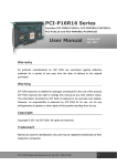
1
DM300/DM5300 User's Manual
RTD Embedded Technologies Inc.
(Real Time Devices)
“Accessing the Analog World”®
ISO9001 and AS9100 Certified
BDM-610010021
Rev. A
DM300/DM5300
User's Manual
RTD Embedded Technologies, INC.
103 Innovation Blvd.
State College, PA 16803-0906
Phone: +1-814-234-8087
FAX: +1-814-234-5218
E-mail
[email protected]
[email protected]
web site
http://www.rtd.com
Revision History
Rev. A
New manual naming method
Published by:
RTD Embedded Technologies, Inc.
103 Innovation Blvd.
State College, PA 16803-0906
Copyright 1999, 2002, 2003 by RTD Embedded Technologies, Inc.
All rights reserved
Printed in U.S.A.
The RTD Logo is a registered trademark of RTD Embedded Technologies. cpuModule and utilityModule are trademarks
of RTD Embedded Technologies. PhoenixPICO and PheonixPICO BIOS are trademarks of Phoenix Technologies Ltd.
PS/2, PC/XT, PC/AT and IBM are trademarks of International Business Machines Inc. MS-DOS, Windows, Windows
95, Windows 98 and Windows NT are trademarks of Microsoft Corp. PC/104 is a registered trademark of PC/104
Consortium. All other trademarks appearing in this document are the property of their respective owners.
TABLE OF CONTENTS
INTRODUCTION .................................................................................................................................... i-1
Analog-to-Digital Conversion ................................................................................................................................. i-3
Digital-to-Analog Conversion ................................................................................................................................. i-4
Digital I/O ............................................................................................................................................................... i-4
What Comes With Your Board ............................................................................................................................... i-4
Board Accessories ................................................................................................................................................... i-4
Hardware Accessories ............................................................................................................................................. i-4
Using This Manual .................................................................................................................................................. i-4
When You Need Help ............................................................................................................................................. i-5
CHAPTER 1 — MODULE SETTINGS ............................................................................................... 1-1
Factory-Configured Switch and Jumper Settings .................................................................................................. 1-3
P3 — User Timer/Counter Output Select (Factory Setting: P2-43: TRIG, P2-44: OT0) .................................. 1-4
P4 — User Timer/Counter Clock Source (Factory Settings: CLK0-OSC, CLK1-OT0, CLK2-OT1) .............. 1-4
P5 — User Timer/Counter Gate Source (Factory Settings: All Gates: +5V) .................................................... 1-5
P6 — Single-Ended/Differential Analog Inputs (Factory Setting: S (16 Single-Ended)) ................................ 1-6
P7 — Analog Input Voltage Range and Polarity (Factory Setting: 5V, BI (±2.5 Volts)) ................................. 1-6
P8 — DAC 1 Output Voltage Range (Factory Setting: +5 to -5 volts) ............................................................. 1-6
P9 — DAC 2 Output Voltage Range (Factory Setting: +5 to -5 volts) ............................................................. 1-7
S1 — Base Address (Factory Setting: 300 hex (768 decimal)) ......................................................................... 1-8
Pull-up/Pull-down Resistors on Digital I/O Lines ................................................................................................. 1-9
J4 — Trigger Input Select (Factory Setting: TR) ................................................................................................ 1-10
Gm, Gain Multiplier Circuitry ............................................................................................................................. 1-10
CHAPTER 2 — MODULE INSTALLATION .................................................................................... 2-1
Module Installation ................................................................................................................................................ 2-3
External I/O Connections ....................................................................................................................................... 2-3
Connecting the Analog Input Pins ..................................................................................................................... 2-4
Connecting the Trigger In and Trigger Out Pins, Cascading Boards ................................................................ 2-5
Connecting the Analog Outputs......................................................................................................................... 2-6
Connecting the Timer/Counters and Digital I/O ............................................................................................... 2-6
Running the 5300DIAG Diagnostics Program ...................................................................................................... 2-6
CHAPTER 3 — HARDWARE DESCRIPTION ................................................................................. 3-1
A/D Conversion Circuitry ...................................................................................................................................... 3-3
Analog Inputs ..................................................................................................................................................... 3-3
V/F Converter .................................................................................................................................................... 3-4
Timing and Counting Circuits ........................................................................................................................... 3-5
D/A Converter ........................................................................................................................................................ 3-5
Timer/Counters ...................................................................................................................................................... 3-5
Digital I/O, Programmable Peripheral Interface .................................................................................................... 3-6
Interrupts ................................................................................................................................................................ 3-7
DM300/DM5300 dataModule™
i
RTD Embedded Technologies, Inc.
CHAPTER 4 — MODULE OPERATION AND PROGRAMMING ................................................ 4-1
Defining the I/O Map ............................................................................................................................................. 4-3
BA + 0: A/D Data Low Byte (Read Only) ....................................................................................................... 4-4
BA + 1: A/D Data Middle Byte (Read Only) ................................................................................................... 4-4
BA + 2: A/D Data High Byte (Read Only) ....................................................................................................... 4-4
BA + 3: Board Ready/Clear 20-bit Conversion Counter (Read/Write) ........................................................... 4-4
BA + 4: 8254 Timer/Counter 0 (Read/Write) .................................................................................................. 4-4
BA + 5: 8254 Timer/Counter 1 (Read/Write) .................................................................................................. 4-5
BA + 6: 8254 Timer/Counter 2 (Read/Write) .................................................................................................. 4-5
BA + 7: 8254 Control Word (Write Only) ....................................................................................................... 4-5
BA + 8: PPI Port A — Digital I/O (Read/Write) .............................................................................................. 4-5
BA + 9: PPI Port B — Channel/Gain Select (Read/Write) .............................................................................. 4-5
BA + 10: PPI Port C — Digital I/O (Read/Write) ............................................................................................. 4-6
BA + 11: 8255 PPI Control Word (Write Only) .............................................................................................. 4-6
BA + 12: D/A Converter 1 LSB (Read/Write) ................................................................................................. 4-8
BA + 13: D/A Converter 1 MSB (Read/Write) ................................................................................................ 4-8
BA + 14: D/A Converter 2 LSB (Read/Write) ................................................................................................. 4-8
BA + 15: D/A Converter 2 MSB (Read/Write) ................................................................................................ 4-8
BA + 16: User 8254 Timer/Counter 0 (Read/Write) ........................................................................................ 4-8
BA + 17: User 8254 Timer/Counter 1 (Read/Write) ........................................................................................ 4-8
BA + 18: User 8254 Timer/Counter 2 (Read/Write) ........................................................................................ 4-9
BA + 19: User 8254 Control Word (Write Only) ............................................................................................. 4-9
BA + 20: Board Setup Register (Write Only) .................................................................................................. 4-9
BA + 21: A/D Trigger Mode Register (Write Only) ...................................................................................... 4-10
BA + 22: Reset/Update DACs (Read/Write) .................................................................................................. 4-10
A/D Conversions .................................................................................................................................................. 4-11
Programming the 8254 Timer .......................................................................................................................... 4-11
Initializing the 8255 PPI .................................................................................................................................. 4-12
Clearing the Board ........................................................................................................................................... 4-13
Setting the Channel .......................................................................................................................................... 4-13
Setting the Gain ............................................................................................................................................... 4-13
Conversion Modes ........................................................................................................................................... 4-14
Single Convert Mode ................................................................................................................................... 4-14
Continuous Convert Mode .......................................................................................................................... 4-16
Cascading Boards ........................................................................................................................................ 4-18
Reading the Converted Data ............................................................................................................................ 4-19
D/A Conversions .................................................................................................................................................. 4-19
User-Available 8254 Timer/Counter ................................................................................................................... 4-21
Digital I/O ............................................................................................................................................................ 4-22
Interrupts .............................................................................................................................................................. 4-22
Example Programs ............................................................................................................................................... 4-23
C and Pascal Programs .................................................................................................................................... 4-23
BASIC Programs ............................................................................................................................................. 4-23
CHAPTER 5 — CALCULATING FREQUENCIES, VOLTAGES, AND BITS ............................. 5-1
Calculating the Settings for the 8254 Timer .......................................................................................................... 5-3
Binary Calculations ........................................................................................................................................... 5-3
Decimal Calculations ......................................................................................................................................... 5-5
Conversion Results and Correction Factor ............................................................................................................ 5-7
Input Voltages and Output Frequencies ................................................................................................................. 5-8
Input Voltage Calculations ..................................................................................................................................... 5-9
Bit Calculations ...................................................................................................................................................... 5-9
DM300/DM5300 dataModule™
ii
RTD Embedded Technologies, Inc.
CHAPTER 6 — CALIBRATION ......................................................................................................... 6-1
Required Equipment .............................................................................................................................................. 6-3
V/F Calibration....................................................................................................................................................... 6-3
D/A Calibration ...................................................................................................................................................... 6-4
APPENDIX A — DM5300 SPECIFICATIONS .................................................................................. A-1
APPENDIX B — P2 CONNECTOR PIN ASSIGNMENTS ............................................................... B-1
APPENDIX C — COMPONENT DATA SHEETS............................................................................. C-1
APPENDIX D — WARRANTY ............................................................................................................ D-1
DM300/DM5300 dataModule™
iii
RTD Embedded Technologies, Inc.
DM300/DM5300 dataModule™
iv
RTD Embedded Technologies, Inc.
LIST OF ILLUSTRATIONS
1-1
1-2
1-3
1-4
1-5
1-6
1-7
1-8
1-9
1-10
1-11
1-12
1-13
1-14
2-1
2-2
2-3
2-4
3-1
3-2
3-3
4-1
4-2
4-3
4-4
4-5
4-6
6-1
Module Layout Showing Factory-Configured Settings ........................................................................... 1-3
User Timer/Counter Output Select Jumpers, P3 ...................................................................................... 1-4
User Timer/Counter Clock Source Jumpers, P4 ...................................................................................... 1-4
8254 Timer/Counter Circuit Block Diagram ........................................................................................... 1-5
User Timer/Counter Gate Source Jumpers, P5 ........................................................................................ 1-5
Single-Ended/Differential Analog Input Signal Type Jumpers, P6 ......................................................... 1-6
Analog Input Voltage Range and Polarity, P7 ......................................................................................... 1-6
DAC 1 Output Voltage Range Jumper, P8 .............................................................................................. 1-7
DAC 2 Output Voltage Range Jumper, P9 .............................................................................................. 1-7
Base Address Switch, S1 .......................................................................................................................... 1-8
Adding Pull-ups and Pull-downs to Digital I/O Lines ........................................................................... 1-10
J4, Trigger Input Select .......................................................................................................................... 1-10
Gain Circuitry and Formula for Calculating Gm ................................................................................... 1-11
Diagram for Removal of Solder Short ................................................................................................... 1-11
P2 I/O Connector Pin Assignments .......................................................................................................... 2-4
Single-Ended Input Connections .............................................................................................................. 2-4
Differential Input Connections ................................................................................................................. 2-5
Cascading Two Boards for Simultaneous Sampling ................................................................................ 2-6
DM5300 Block Diagram .......................................................................................................................... 3-3
V/F Timing and Counting Block Diagram ............................................................................................... 3-4
User 8254 Timer/Counter Circuitry ......................................................................................................... 3-6
Single Convert Mode Timing Diagram .................................................................................................. 4-14
Single Convert Mode Flow Diagram ..................................................................................................... 4-15
Continuous Convert Mode Timing Diagram ......................................................................................... 4-16
Continuous Convert Mode Flow Diagram ............................................................................................. 4-17
Cascaded Boards, Single Convert Mode Flow Diagram ........................................................................ 4-18
User 8254 Timer/Counter Circuitry ....................................................................................................... 4-21
Module Layout ......................................................................................................................................... 6-3
DM300/DM5300 dataModule™
v
RTD Embedded Technologies, Inc.
DM300/DM5300 dataModule™
vi
RTD Embedded Technologies, Inc.
Introduction
INTRODUCTION
DM300/DM5300 dataModule™
i-1
RTD Embedded Technologies, Inc.
DM300/DM5300 dataModule™
i-2
RTD Embedded Technologies, Inc.
Introduction
The DM5300 variable resolution integrating analog dataModule turns your IBM PC/XT/AT
compatible cpuModule or other PC/104 computer into a high-performance data acquisition and
control system. Ultra-compact for embedded and portable applications, the DM5300 features:
•
•
•
•
•
•
•
•
•
•
•
•
8 differential or 16 single-ended analog input channels,
Resolution to 18 bits using a synchronous voltage-to-frequency converter,
0 to +5, 0 to +10, ±2.5, or ±5 volt input range,
Programmable gains of 1, 2, 4, and 8 with an on-board gain multiplier circuit,
Clock controlled A/D conversion,
Software selectable system clock interrupt source and interrupt channel,
Trigger in and trigger out for external triggering or cascading boards,
Two 12-bit analog output channels,
±5, ±10, 0 to +5, or 0 to +10 volt analog output range,
Three user available 16-bit timer/counters,
16 8255-based TTL/CMOS compatible digital I/O lines,
+5 volt operation (DM5300).
The following paragraphs briefly describe the major functions of the module. More detailed
discussions of module functions are included in Chapter 3, Hardware Description, and Chapter 4,
Module Operation and Programming. The module setup is described in Chapter 1, Module
Settings.
The difference between the DM300 and the DM5300 modules is in the power supply requirements.
The DM300 module needs a +5, +12, and -12 volt supply for proper operation. The DM5300
module needs only a +5 volt power supply, making it ideal for portable applications.
Analog-to-Digital Conversion
The analog-to-digital (A/D) conversion circuitry receives up to eight differential or 16 singleended analog inputs and converts these inputs into frequencies. The frequencies are represented by
20-bit plus overflow words (in 3 x 8-bit format) which are read and/or transferred to PC memory.
An on-board header connector lets you jumper the inputs for differential or single-ended operation.
Two unipolar and two bipolar ranges can be selected: 0 to +5, 0 to +10, ±2.5, or ±5 volts. The
module is calibrated at the factory for ±2.5 volts. Software programmable gains of 1, 2, 4, and 8
with an on-board gain multiplier circuitry let you customize the input range. Over voltage protection to ±35 volts is provided at the inputs.
A/D conversions are performed by a voltage-to-frequency (V/F) converter. This exceptionally
accurate converter technology lets you vary the resolution of your conversion while maintaining
the full input voltage range. For example, with a 1 MHz system clock and the input range set for 5
volts, 10-bit conversions are performed at a rate of 488 samples per seconds with a resolution of
4.88 millivolts, 12-bit conversions are performed at a rate of 122 samples per second with a
resolution of 1.22 millivolts, and 18-bit conversions are performed at a rate of 2 samples per
second with a resolution of 19 microvolts.
The converted data is read and/or transferred to PC memory, one byte at a time, through the PC
data bus.
DM300/DM5300 dataModule™
i-3
RTD Embedded Technologies, Inc.
Digital to Analog Conversion
Digital-to-Analog Conversion
The digital-to-analog (D/A) circuitry features two independent 12-bit analog output channels with
individually jumper-selectable output ranges of -5 to +5 volts, -10 to +10 volts, 0 to +5 volts, or 0
to +10 volts. Data is programmed into the D/A converter by writing two 8-bit words, the LSB and
the MSB. Both outputs can be simultaneously updated by writing to an I/O port.
Digital I/O
The DM5300 has 16 TTL/CMOS compatible digital I/O lines which can be directly interfaced
with external devices or signals to sense switch closures, trigger digital events, or activate solidstate relays. These lines are provided by the 8255 programmable peripheral interface (PPI). Pads
for activating pull-up/pull-down resistors are included on the module. Installation procedures are
given near the end of Chapter 1, Module Settings.
What Comes With Your Module
You receive the following items in your DM5300 package:
•
•
•
•
DM5300 analog I/O dataModule
Mounting hardware
Software and diagnostics diskette with example programs in BASIC and C
User’s manual
If any item is missing or damaged, please call RTD Embedded Technologies Inc. Customer
Service Department at (814) 234-8087. If you require service outside the U.S., contact your local
distributor.
Module Accessories
In addition to the items included in your DM5300 package, RTD Embedded Technologies Inc.
offers a full line of software and hardware accessories. Call your local distributor or our main
office for more information about these accessories and for help in choosing the best items to
support your module’s application.
Hardware Accessories
Hardware accessories for the DM5300 include the TMX32 analog input expansion board with
thermocouple compensation which can expand a single input channel on your board to 16 differential or 32 single-ended input channels, MR series mechanical relay output boards, OP series
optoisolated digital input boards, the OR16 mechanical relay/optoisolated digital I/O board, the
USF4 universal sensor front-end with sensor excitation, the TB50 terminal board and XB50
prototype/terminal board for prototype development and easy signal access, the DM14 extender
board for simplified testing and debugging of prototype circuitry, and the XT50 twisted pair ribbon
cable assembly for external interfacing.
Using This Manual
This manual is intended to help you install your new module and get it running quickly, while also
providing enough detail about the module and its functions so that you can enjoy maximum use of
DM300/DM5300 dataModule™
i-4
RTD Embedded Technologies, Inc.
Introduction
its features even in the most complex applications. We assume that you already have an understanding of data acquisition principles and that you can customize the example software or write
your own applications programs.
When You Need Help
This manual and the example programs in the software package included with your module provide
enough information to properly use all of the module’s features. If you have any problems installing or using this module, contact our Technical Support Department, (814) 234-8087, during
regular business hours, eastern standard time or eastern daylight time, or send a FAX requesting
assistance to (814) 234-5218. When sending a FAX request, please include your company’s name
and address, your name, your telephone number, and a brief description of the problem.
DM300/DM5300 dataModule™
i-5
RTD Embedded Technologies, Inc.
DM300/DM5300 dataModule™
i-6
RTD Embedded Technologies, Inc.
Chapter 1 Module Settings
CHAPTER 1 MODULE
SETTINGS
The DM5300 has jumper and switch settings you can change if
necessary for your application. The module is factory-configured as
listed in the table and shown on a diagram in the beginning of this
chapter. Should you need to change these settings, use these easyto-follow instructions before you install the module in your system.
Note that by installing jumpers in the associated pads, you can
configure the 16 available digital I/O lines to be pulled up or pulled
down. This procedure is explained near the end of this chapter.
Also note that by installing resistive components, you can add your
own gain multiplier for the software programmable binary gains of
1, 2, 4, and 8. The gain multiplier circuitry is described at the end
of this chapter.
DM300/DM5300 dataModule™
1-1
RTD Embedded Technologies, Inc.
DM300/DM5300 dataModule™
1-2
RTD Embedded Technologies, Inc.
Chapter 1 Module Settings
Factory-Configured Switch and Jumper Settings
Table 1-1 lists the factory settings of the user-configurable switch and jumpers on the DM5300.
Figure 1-1 shows the module layout and the locations of the factory-set jumpers. The following
paragraphs explain how to change the factory settings.
Table 1-1 Factory Settings
Switch/Jump
Function Controlled
Factory Settings
P3
Sets the user timer/counter output signals
available at P2-43 and P2-44
P2-43: TRIG, P2-44: OUT0
P4
Sets the clock sources for the user
timer/counters
CLK0:OSC, CLK1:OT0,
CLK2:OT1 (cascaded)
P5
Sets the gate sources for the user
timer/counters
GATE0:+5V, GATE1:+5V,
GATE2:+5V
P6
Sets the analog input as 16 single-ended or 8
differential
16 single-ended (3
jumpers installed on S
pins)
P7
Sets the analog input voltage range and
polarity
5V, BI (-2.5 to +2.5 volts)
P8
Sets the D/A output voltage range for DAC 1
+-5, X1 (-5 to +5 volts)
P9
Sets the D/A output voltage range for DAC 2
+-5, X1 (-5 to +5 volts)
S1
Sets the base address
300 hex (768 decimal)
J4
Connects TRIGGER IN (P2-39) or
TIMER/COUNTER 2 out 2 to EPLD trigger input
TRIGGER IN (P2-39)
S1 BASE ADDRESS
TR2
TR1
TR3 R11 R10
TR4
TR5
U14
HI-508A
4SPST
C40
P2
R7
R8
C38
C20
PGA203
R9
C48
R12
R1
HI-508A
R13
R14
U11
+
P3
U15
P7
5
10
UN
BI
AD652
S
D
S
D
S
D
R6
U18
RN2
P6
U16
C49
TRIG
OUT2
OUT0
OUT1
P8
U
B
1
2
C8
EPLD
U13
AD712
RN9
OSC P4
EC1
EC2
OUT0
OSC
EC1
EC2
OUT1
OSC
EC1
EC2
P9
U
B
1
2
AD7237
U6
74LS244
C9
+5V P5
EGT1
EGT2
+5V
EGT1
EGT2
+5V
EGT1
EGT2
82C55
V
XTAL1
C6
82C54
82C54
J1
C7
J4
Y1
P1
B1
U10
U8
G
U5 U4
TR
J2
J3
O2
B32
A1
A32
+
DC1
J6
FB1
R
J5
Copyright C 1995 Real Time Devices Europa Kft.
Made in Hungary
Fig. 1-1 — Module Layout Showing Factory-Configured Settings
DM300/DM5300 dataModule™
1-3
RTD Embedded Technologies, Inc.
Factory-Configured Switch and Jumper Settings
P3 -User Timer/Counter Output Select (Factory Setting: P2-43: TRIG, P2-44: OUT0)
This header connector, shown in Figure 1-2, lets you select one of two signals to be present at each
of two of the P2 I/O connector pins, P2-43 and P2-44. This allows you more flexibility when
setting up the module. P2-43 can be configured to provide an external trigger (TRIG) or the output
of user timer/counter 2 (OUT2). P2-44 can be configured to provide the output of user timer/
counter 0 (OUT0) or the output of user timer/counter 1 (OUT1). Note that when you cascade
multiple modules, you must configure P2-43 to carry the external trigger signal (TRIG) on each
module that outputs a trigger to the next module in the chain.
P3
43
TRIG
OUT2
P2
OUT0
OUT1
44
Fig. 1-2 — User Timer/Counter Output Select Jumpers, P3
P4 - User Timer/Counter Clock Source (Factory Settings: CLK0-OSC, CLK1-OUT0, CLK2OUT1)
This header connector, shown in Figure 1-3, lets you select the clock sources for the user available
8254 timer/counters, TC0, TC1, and TC2. The factory setting cascades all three timer/counters,
with the clock source for TC0 being the on-board 2 MHz oscillator, the output of TC0 providing
the clock for TC1, and the output of TC1 providing the clock for TC2. You can connect any or all
of the sources to either of two external clock inputs (the first source labeled EC1 on the header is
EXT CLK1 at P2-41, and the second source labeled EC2 on the header is EXT CLK2 at P2-45), or
you can set TC1 and TC2 to be clocked by the 2 MHz oscillator. Figure 1-4 shows a block diagram
of the timer/counter circuitry to help you with these connections.
NOTE: When installing jumpers on this header, make sure that only one jumper is installed in
P4
CLK0
OSC
EC1
EC2
OUT0
CLK1
OSC
EC1
EC2
OUT1
CLK2
OSC
EC1
EC2
Fig. 1-3 — User Timer/Counter Clock Source Jumpers, P4
DM300/DM5300 dataModule™
1-4
RTD Embedded Technologies, Inc.
Chapter 1 Module Settings
P4
DM5300
I/O CONNECTOR
P2
2 MHz
(XTAL)
8254 PIT
OSC
PIN 41
EC1
TIMER/
COUNTER
0
CLK
PIN 45
EC2
+5V
P5
PIN 42
+5V
PIN 46
EGT1
GATE
EGT2
EXTCLK1
EXTCLK2
EXTGATE1
EXTGATE2
P3
OU T0
OUT
PIN 44
OUT0 / OUT1
OU T1
OU T0
OSC
+5V
EC1
TIMER/
COUNTER
1
CLK
EC2
+5V
EGT1
GATE
EGT2
OUT
OU T1
OSC
+5V
EC1
TIMER/
COUNTER
2
CLK
EC2
+5V
EGT1
GATE
EGT2
OU T2
OUT
PIN 43
TRIG
TRIGGER
OUT / OUT2
EXTERNAL
TRIGGER
OUT
Fig. 1-4 — 8254 Timer/Counter Circuit Block Diagram
each group of CLK pins.
P5 — User Timer/Counter Gate Source (Factory Settings: All Gates: +5V)
This header connector, shown in Figure 1-5, lets you select the gate sources for the user available
8254 timer/counters, TC0, TC1, and TC2. The factory setting ties all three gates high, to an onboard +5 volt source. You can connect any or all of the gates to either of two external gate inputs
(the first source labeled EGT1 on the header is EXT GATE1 at P2-42, and the second source
labeled EGT2 on the header is EXT GATE2 at P2-46). Figure 1-4 shows a block diagram of the
GATE0
+5V
P5
EGT1
EGT2
GATE1
+5V
EGT1
EGT2
GATE2
+5V
EGT1
EGT2
Fig. 1-5 — User Timer/Counter Gate Source Jumpers, P5
DM300/DM5300 dataModule™
1-5
RTD Embedded Technologies, Inc.
Factory-Configured Switch and Jumper Settings
timer/counter circuitry to help you with these connections.
NOTE: When installing jumpers on this header, make sure that only one jumper is installed in
each group of GATE pins.
P6 — Single-Ended/Differential Analog Inputs (Factory Setting: S (16 Single-Ended))
P6
S
D
S
D
S
D
Fig. 1-6 — Single-Ended/Differential Analog Input Signal Type Jumpers, P6
This header connector, shown in Figure 1-6, is used to configure the DM5300 for 8 differential or
16 single-ended analog input channels. When operating in the 16 input single-ended mode, three
jumpers must be installed across the S pins. When operating in the 8 input differential mode, three
jumpers must be installed across the D pins. DO NOT install jumpers across both S and D pins at
the same time!
P7 — Analog Input Voltage Range and Polarity (Factory Setting: 5V, BI (±2.5 Volts)
P7, shown in Figure 1-7, sets the analog input voltage range and polarity. The module can be set up
P7
5V
10V
UNI
BI
Fig. 1-7 — Analog Input Voltage Range and Polarity, P7
to operate over a range of 5 or 10 volts, unipolar or bipolar. The module’s four possible ranges are
0 to +5, 0 to +10, ±2.5, and ±5 volts. Figure 1-7 shows the factory setting of -2.5 to +2.5 volts.
NOTE: If you change the analog input range and/or polarity, you should recalibrate the board
according to the instructions in Chapter 6, Calibration. Otherwise, you may get erroneous data.
P8 — DAC 1 Output Voltage Range (Factory Setting: +5 to -5 volts)
DM300/DM5300 dataModule™
1-6
RTD Embedded Technologies, Inc.
Chapter 1 Module Settings
Jumpers (Top to Bottom)
X1
X2
-5 to +5 volts
OFF
ON
ON
OFF
0 to +5 volts
ON
OFF
ON
OFF
-10 to +10 volts
OFF
ON
OFF
ON
0 to +10 volts
ON
OFF
OFF
ON
P8
DAC1
X2
X1
B
B
U
U
Voltage Range
Fig. 1-8 — DAC 1 Output Voltage Range Jumper, P8
This header connector, shown in Figure 1-8, sets the output voltage range for DAC 1 at 0 to +5,
±5, 0 to +10, or ±10 volts. Two jumpers must be installed, one to select the range and one to select
the multiplier. The first two positions select the range, bipolar (±5) or unipolar (5). The next two
positions select the multiplier, X2 or X1. When a jumper is on the X2 multiplier pins, the range
values become ±10 and 10. The table on the next page shows the four possible combinations of
jumper settings. This header does not have to be set the same as P9.
Jumpers (Top to Bottom)
X2
-5 to +5 volts
OFF
ON
ON
OFF
0 to +5 volts
ON
OFF
ON
OFF
-10 to +10 volts
OFF
ON
OFF
ON
0 to +10 volts
ON
OFF
OFF
ON
DAC2
P9
X2
X1
X1
B
B
U
U
Voltage Range
Fig. 1-9 — DAC 2 Output Voltage Range Jumper, P9
DM300/DM5300 dataModule™
1-7
RTD Embedded Technologies, Inc.
Factory-Configured Switch and Jumper Settings
P9 — DAC 2 Output Voltage Range (Factory Setting: +5 to -5 volts)
This header connector, shown in Figure 1-9, sets the output voltage range for DAC 2 at 0 to +5,
±5, 0 to +10, or ±10 volts. Two jumpers must be installed, one to select the range and one to select
the multiplier. The first two positions select the range, bipolar (±5) or unipolar (5). The next two
positions select the multiplier, X2 or X1. When a jumper is on the X2 multiplier pins, the range
values become ±10 and 10. The table below shows the four possible combinations of jumper
settings. This header does not have to be set the same as P8.
S1 — Base Address (Factory Setting: 300 hex (768 decimal))
One of the most common causes of failure when you are first trying your module is address
contention. Some of your computer’s I/O space is already occupied by internal I/O and other
peripherals. When the DM5300 attempts to use I/O address locations already used by another
device, contention results and the module does not work.
Table 1-2 Base Address Switch Settings, S1
Base Address
Switch Setting
Decimal / (Hex)
4321
512 / (200)
0000
544 / (220)
0001
576 / (240)
0010
608 / (260)
0011
640 / (280)
0100
672 / (2A0)
0101
704 / (2C0)
0110
736 / (2E0)
0111
0 = Closed, 1 = Open
Base Address
Decimal / (Hex)
768 / (300)
800 / (320)
832 / (340)
864 / (360)
896 / (380)
928 / (3A0)
960 / (3C0)
992 / (3E0)
Switch Setting
4321
1000
1001
1010
1011
1100
1101
1110
1111
Fig. 1-10 — Base Address Switch, S1
DM300/DM5300 dataModule™
1-8
RTD Embedded Technologies, Inc.
Chapter 1 Module Settings
To avoid this problem, the DM5300 has an easily accessible four-position DIP switch, S1, which
lets you select any one of 16 starting addresses in the computer’s I/O. Should the factory setting of
300 hex (768 decimal) be unsuitable for your system, you can select a different base address
simply by setting the switches to any one of the values listed in Table 1-2. The table shows the
switch settings and their corresponding decimal and hexadecimal (in parentheses) values. Make
sure that you verify the order of the switch numbers on the switch (1 through 4) before setting
them. When the switches are pulled forward, they are OPEN, or set to logic 1, as labeled on the
DIP switch package. When you set the base address for your module, record the value in the table
inside the back cover. Figure 1-10 shows the DIP switch set for a base address of 300 hex (768
decimal).
Pull-up/Pull-down Resistors on Digital I/O Lines
The 8255 programmable peripheral interface provides 16 TTL/CMOS compatible digital I/O lines
which can be interfaced with external devices. These lines are divided into three groups: eight Port
A lines, four Port C Lower lines, and four Port C Upper lines. (The eight lines of Port B are used
for internal board functions.) You can connect pull-up or pull-down resistors for any or all of these
three groups of lines. You may want to pull lines up for connection to switches. This will pull the
line high when the switch is disconnected. Or, you may want to pull lines down for connection to
relays which control turning motors on and off. These motors turn on when the digital lines
controlling them are high. The Port A lines of the 8255 automatically power up as inputs, which
can float high during the few moments before the board is first initialized. This can cause the
external devices connected to these lines to operate erratically. By pulling these lines down, when
the data acquisition system is first turned on, the motors will not switch on before the 8255 is
+5 V
PA
8255
V
PUL L - UP
G
10K
PORT A
( PA 0 - 7 )
+5 V
CL
PUL L - DOWN
V
G
10K
PORT C
L OWER
( PC0 - 3 )
+5 V
CH
V
G
PORT C
UPPER
( PC4 - 7 )
Fig. 1-11 — Adding Pull-ups and Pull-downs to Digital I/O Lines
DM300/DM5300 dataModule™
1-9
RTD Embedded Technologies, Inc.
initialized.
To use the pull-up/pull-down feature, you must connect them into the circuit as pull-ups or pulldowns. Locate the three-hole pads (J1, J2, J3) on the board below the P2 connector. They are
labeled G (for ground) on one end and V (for +5V) on the other end. The middle hole is common.
J1 is for Port A, J2 is for Port C Lower, and J3 is for Port C Upper. To operate as pull-ups, solder a
jumper wire between the common pin (middle pin of the three) and the V pin. For pull-downs,
solder a jumper wire between the common pin (middle pin) and the G pin. Figure 1-11 shows Port
A lines with pull-ups, Port C Lower with pull-downs, and Port C Upper with no resistors.
J4 — Trigger Input Select (Factory Setting: TR)
This header connector, shown in Figure 1-12, is used to select the input for the triggering circuit.
J4
TR
O2
Fig. 1-12 — J4, Trigger Input Select
The two options are TR (TRIGGER IN P2-39) or O2 (user TIMER/COUNTER OUT2). This
jumper is used in conjunction with the trigger and interrupt mode set in the register at BA +21. For
example, if you would like to use an external signal to trigger the conversion, you would connect
your trigger signal to P2-39, set jumper J4 for TR, and program the trigger select at BA +21 (bit
D0) for External Trigger.
If you would like to use this timer/counter to trigger the conversions, you would set J4 for O2 and
program the trigger select for External Trigger. If you would like to use internal triggering but use
the timer to generate interrupts, you would set J4 for O2 and program the trigger register to internal
triggering and the IRQ select to External Trigger.
Gm, Gain Multiplier Circuitry
The DM5300 has software programmable binary gains of 1, 2, 4, and 8. A gain multiplier circuit,
Gm, is provided so that you can easily configure special gain settings for a specific application.
Note that when you use this feature and set up the module for a gain of other than 1, all of the input
channels will operate only at your custom gain settings. In other words, if you install circuitry
which gives you a gain multiplier of 10, then the four programmable gains available are 10, 20, 40,
and 80.
Gm is derived by adding resistors R10 and R11 and trimpot TR3, all located in the upper center
area of the module. The resistors and trimpot combine to set the gain, as shown in the diagram and
formula in Figure 1-13.
As shown in Figure 1-13, a solder short labeled J7 must be removed from the module to activate
the Gm circuitry. This short is located on the bottom side of the board under R10 and R11. Figure
1-14 shows the location of the solder short.
DM300/DM5300 dataModule™
1-10
RTD Embedded Technologies, Inc.
Chapter 1 Module Settings
3
2
Remove solder short
(see Figure 1-14)
+
U17
1
-
TR3
R11
R10
To calculate Gm:
Gm =[(TR3 + R11)/R10] + 1
Fig. 1-13 — Gain Circuitry and Formula for Calculating Gm
TR3 R11 R10
TR4
Remove Solder Short
Between These 2 Pads on
Bottom Side of Board
Fig. 1-14 — Diagram for Removal of Solder Short
DM300/DM5300 dataModule™
1-11
RTD Embedded Technologies, Inc.
DM300/DM5300 dataModule™
1-12
RTD Embedded Technologies, Inc.
Chapter 2 Module Installation
CHAPTER 2 MODULE INSTALLATION
The DM5300 board is easy to install on your cpuModule or other
PC/104 system. This chapter tells you step-by-step how to install
and connect the module.
After you have installed the module and made all of your connections, you can turn your system on and run the 5300DIAG diagnostics program included on your example software disk to verify that
your module is working.
DM300/DM5300 dataModule™
2-1
RTD Embedded Technologies, Inc.
DM300/DM5300 dataModule™
2-2
RTD Embedded Technologies, Inc.
Chapter 2 Module Installation
Module Installation
Keep the module in its antistatic bag until you are ready to install it in your cpuModule™ or other
PC/104 based system. When removing it from the bag, hold the module at the edges and do not
touch the components or connectors.
Before installing the module in your system, check the jumper settings. Chapter 1 reviews the
factory settings and how to change them. If you need to change any settings, refer to the appropriate instructions in Chapter 1. Note that incompatible jumper settings can result in unpredictable
module operation and erratic response.
The DM5300 comes with a stackthrough P1 connector. The stackthrough connector lets you stack
another module on top of your DM5300.
To install the module, follow the procedures described in the computer manual and the steps
below:
1.
Turn OFF the power to your system.
2.
Touch a metal rack to discharge any static buildup and then remove the module from its
antistatic bag.
3.
Select the appropriate standoffs for your application to secure the module when you install it
in your system (two sizes are included with the module).
4.
Holding the module by its edges, orient it so that the P1 bus connector's pin 1 lines up with pin
1 of the expansion connector onto which you are installing the module.
5.
After carefully positioning the module so that the pins are lined up and resting on the expansion connector, gently and evenly press down on the module until it is secured on the connector.
NOTE: Do not force the module onto the connector. If the module does not readily press into
place, remove it and try again. Wiggling the module or exerting too much pressure can result
in damage to the DM5300 or to the mating module.
6.
After the module is installed, connect the cable to I/O connector P2 on the module. When
making this connection, note that there is no keying to guide you in orientation. You must
make sure that pin 1 of the cable is connected to pin 1 of P2 (pin 1 is marked on the module
with a small square). For twisted pair cables, pin 1 is the dark brown wire; for standard single
wire cables, pin 1 is the red wire.
7.
Make sure all connections are secure.
External I/O Connections
Figure 2-1 shows the DM5300’s P2 I/O connector pinout. Refer to this diagram as you make your
I/O connections. Note that the +12 and -12 volt signals are available at pins 47 and 49 only if your
system power supply provides these voltages.
DM300/DM5300 dataModule™
2-3
RTD Embedded Technologies, Inc.
External I/O Connections
DIFF.
S.E.
DIFF.
S.E.
AIN1+
AIN1
1
2
AIN1-
AIN9
AIN2+
AIN2
3
4
AIN2-
AIN10
AIN3+
AIN3
5
6
AIN3-
AIN11
AIN4+
AIN4
7
8
AIN4-
AIN12
AIN4+
AIN5
9
10
AIN5-
AIN13
AIN6+
AIN6
11 12
AIN6-
AIN14
AIN7+
AIN7
13 14
AIN7-
AIN15
AIN8+
AIN8
15 16
AIN8-
AIN16
AOUT 1
17 18
ANALOG GND
AOUT 2
19 20
ANALOG GND
ANALOG GND
21 22
ANALOG GND
PA7
23 24
PC7
PA6
25 26
PC6
PA5
27 28
PC5
PA4
29 30
PC4
PA3
31 32
PC3
PA2
33 34
PC2
PA1
35 36
PC1
PA0
37 38
PC0
TRIGGER IN
39 40
DIGITAL GND
EXT CLK1
41 42
EXT GATE1
TRIGGER OUT / OUT2
43 44
OUT0 / OUT1
EXT CLK2
45 46
EXT GATE2
+12 VOLTS
47 48
+5 VOLTS
-12 VOLTS
49 50
DIGITAL GND
Fig. 2-1 — P2 I/O Connector Pin Assignments
Connecting the Analog Input Pins
16 Single-Ended. When operating in the 16 channel single-ended mode (P6-S), connect the high
side of the analog inputs to the analog input channels, AIN1 through AIN16, and connect the low
side to any of the ANALOG GND pins available at the connector (pins 18, 20-22 on P2). Ground
any unused inputs. Figure 2-2 shows how these connections are made.
DM5300
I / O C O N N E C TO R
P2
SIGNAL
SOURCE
1 OUT
+
PIN 1
AIN 1
GND
MUX
SIGNAL
SOURCE
15 OUT
+
P I N 14
OUT +
+
OUT -
-
A I N 15
GND
P I N 16
A I N 16
P I N 22
Fig. 2-2 — Single-Ended Input Connections
DM300/DM5300 dataModule™
2-4
RTD Embedded Technologies, Inc.
Chapter 2 Module Installation
8 Differential. When operating in the differential mode (P6-D), twisted pair cable is recommended to reduce the effects of coupling at the input. Your signal source may or may not have a
separate ground reference. When using the differential mode, you should install a 10 kilohm
resistor pack at RN2 on the board to provide a reference to ground for signal sources without a
separate ground reference.
Connect the high side of the analog input to the selected analog input channel, AIN1+ through
AIN8+, and connect the low side to the corresponding AIN- pin. Then, for signal sources with a
separate ground reference, connect the ground from the signal source to an ANALOG GND (pins
18 and 20-22 on P3). Figure 2-3 shows how these connections are made.
DM5300
I / O C O N N E C TO R
P2
SIGNAL
+
SOURCE
1 OUT
PI N 1
-
PI N 2
AI N 1+
RN2
AI N 110K
MUX
SIGNAL
+
SOURCE
7 OUT
PI N 13
-
PI N 14
OUT +
+
OUT -
-
AI N 7+
AI N 710K
GND
PI N 15
AI N 8+
PI N 16
10K
AI N 8-
PI N 22
Fig. 2-3 — Differential Input Connections
Connecting the Trigger In and Trigger Out Pins, Cascading Modules
The DM5300 has an external trigger input (P2-39) and output (P2-43) so that two or more modules
can be cascaded and run synchronously in a “master/slave” configuration. By cascading two (or
more) modules as shown in Figure 2-5, they can be triggered to start an A/D conversion at the
same time. Note that when using the external trigger output (P2-43) such as on the master module
in Figure 2-4, you must set the jumper on P3 to TRIG.
If you apply an external trigger to the module’s trigger in pin, note that the trigger can be negativeor positive-going. The pulse duration should be at least 100 nanoseconds. When using the TRIGGER OUT, the pulse must always be positive-going.
DM300/DM5300 dataModule™
2-5
RTD Embedded Technologies, Inc.
External I/O Connections
DM5300
I / O C O N N E C TO R
BOARD #1
(MASTER)
MUX
SIGNAL
SOURCE
1 OUT
+
-
P2-1
CH 1
P2-2
CH 1
AI N1 +
AI N1 -
10K
P2-43
T RI GGER OUT
BOARD #2
( S LAV E )
MUX
SIGNAL
SOURCE
2 OUT
+
-
P2-1
CH 1
P2-2
CH 1
10K
AI N1 +
AI N1 -
P2-39
T RI GGER I N
Fig. 2-4 — Cascading Two Modules for Simultaneous Sampling
Connecting the Analog Outputs
For each of the two D/A outputs, connect the high side of the device receiving the output to the
AOUT channel (P2-17 or P2-19) and connect the low side of the device to an ANALOG GND
(P2-18 or P2-20).
Connecting the Timer/Counters and Digital I/O
For all of these connections, the high side of an external signal source or destination device is
connected to the appropriate signal pin on the I/O connector, and the low side is connected to any
DIGITAL GND.
Running the 5300DIAG Diagnostics Program
Now that your module is ready to use, you will want to try it out. An easy-to-use, menu-driven
diagnostics program, 5300DIAG, is included with your example software to help you verify your
module’s operation. You can also use this program to make sure that your current base address
setting does not contend with another device.
DM300/DM5300 dataModule™
2-6
RTD Embedded Technologies, Inc.
Chapter 3 Hardware Description
CHAPTER 3 HARDWARE
DESCRIPTION
This chapter describes the features of the DM5300 hardware. The
major circuits are the A/D which consists of the V/F converter and
associated timing and counting, the D/A, and the digital I/O lines.
Three timer/counters from the user 8254 are available at the I/O
connector for your use. Module interrupts are also described in this
chapter.
DM300/DM5300 dataModule™
3-1
RTD Embedded Technologies, Inc.
DM300/DM5300 dataModule™
3-2
RTD Embedded Technologies, Inc.
Chapter 3 Hardware Description
The DM5300 has three major circuits, the A/D which consists of the V/F converter and associated
timing and counting, the D/A, and the digital I/O lines. Three timer/counters from the user 8254 is
available at the I/O connector for your use. Figure 3-1 shows the block diagram of the board. This
chapter describes hardware which makes up the major circuits. It also discusses interrupts.
20-BIT
MEASUREMENT
COUNTER
DATA
CLK
GATE
ADDRESS
VOLTAGE
-TOFREQUENCY
CONVERTER
ADDRESS
DECODE
CONTROL
16 ANALOG INPUTS
0-10V, ±5V, 0-5V, ±2.5V
8 DIFF./16 S.E.
PROGRAMMABLE
GAIN AMPLIFIER
1/2/4/8
MUX
16
2 MHz
OSC
MEASUREMENT
TIME BASE
SYSTEM CLOCK,
SERVICE TIMER
AND
GATE CONTROL
LOGIC
CLK
OUT
GATE
EXT CLK1
+5V
SAMPLE
COUNTER
EXTERNAL
TRIGGER
LOGIC
TRIGGER IN
PULL-UP/DOWN
RESISTORS
CLK
8
GATE
8
8255
PPI
I/O CONNECTOR
PC BUS
INTERRUPT
SELECT
8
8254
PIT
TIMER/
COUNTER
I/O AND
PACER CLOCK
SELECT
12-BIT
D/A
CONVERTER
RANGE
SELECT
±5 VOLTS
0 +5 VOLTS
±10 VOLTS
5
AOUT1
AOUT2
±12 VOLTS
+5 VOLTS
CONTROL
Fig. 3-1 — DM5300 Block Diagram
A/D Conversion Circuitry
The DM5300 performs analog-to-digital conversions using a voltage-to-frequency converter and
timing and counting circuits. This circuitry functions as an exceptionally accurate integrating
converter. The V/F converter converts the input voltage to a frequency between 0 and system clock
÷ 2 (full scale), and this frequency is counted by the frequency counter for a specified period of
time. The following paragraphs describe the A/D circuitry.
Analog Inputs
The input type can be set for 8 differential or 16 single-ended by setting the jumpers on P6. Singleended operation is typically used when the analog input voltage source is close to the module and
the voltage levels are fairly high (greater than ±0.5 volts). The differential mode provides noise
immunity when long cable runs are unavoidable, signal levels are low, or surrounding electrical
noise is high. Software programmable binary gains of 1, 2, 4, and 8 let you amplify low level
DM300/DM5300 dataModule™
3-3
RTD Embedded Technologies, Inc.
A/D Conversion Circuitry
signals to more closely match the module’s input ranges. These gains can be customized for even
greater input control by adding a gain multiplying resistor circuit as described in Chapter 1.
The input range is jumper-selectable for 5 volts or 10 volts, unipolar or bipolar. The available
ranges are 0 to +5, 0 to +10, -2.5 to +2.5, and -5 to +5 volts. The module is factory set for -2.5 to
+2.5 volts. Should you need to change the input range and/or polarity, you should recalibrate the
board according to the instructions in Chapter 6, Calibration. Each channel has an input impedance of greater than 10 megohms. Overvoltage protection of ±35 Vdc is provided at the multiplexer.
V/F Converter
The V/F converter receives an input voltage and converts it to a corresponding frequency which is
then read from the frequency counter as 20-bit data. The conversion time varies, depending on the
degree of accuracy you want in your result and the speed of the system clock. The software
selectable system clock can be set for 0.5, 1, or 2 MHz. A 1 MHz clock provides the best speed
versus linearity tradeoff for most applications. At 0.5 MHz, linearity improves, but the conversion
time doubles. A 2 MHz clock performs the fastest conversions, but sacrifices linearity. With a
system clock of 1 MHz, a 12-bit conversion is performed in about 8 milliseconds, a 16-bit conversion in 131 milliseconds, and an 18-bit conversion in 524 milliseconds.
The V/F converter used on the DM5300 is Analog Devices’ AD652 monolithic synchronous V/F
converter. This extremely linear device is clocked by the programmable system clock. The system
clock signal is divided by 2 on the chip, resulting in the 0 to system clock ÷ 2 frequency range of
the converter. The same system clock is used to gate the timer circuitry, which means that you will
get accurate conversions even if the clock frequency should drift.
To compensate for gain drift in the V/F converter, a trimpot is provided on the board. Chapter 6,
Calibration, tells you how to adjust this trimpot.
ANALOG
IN
V/F
CONVERTER
CL K
GAT E
20-BIT
COUNTER
SYSTEM
CLOCK
TIMER 0
TIMER 1
OUT
GAT E
CLK
OUT
GAT E
CLK
OUT
GAT E
CLK
CONTROL
LOGIC
TIMER 2
8254 PIT
Fig. 3-2 — V/F Timing and Counting Block Diagram
DM300/DM5300 dataModule™
3-4
RTD Embedded Technologies, Inc.
Chapter 3 Hardware Description
Timing and Counting Circuits
The timing and counting circuits used with the V/F converter are shown in Figure 3-2. Very
simply, the 8254 opens a window of time and the 20-bit counter counts the frequency output of the
V/F converter.
The 20-bit counter has two flags: counter overflow and measurement overflow. The counter
overflow flag is set if the 20-bit counter overflows within a single measurement cycle. The measurement overflow flag is set if two or more measurement cycles have been executed without the
counter being cleared between cycles.
As shown in Figure 3-2, the 8254 programmable interval timer (PIT) contains three 16-bit timers.
Two of these timers are cascaded to form a 32-bit timer which gates the frequency counters. The
frequency counters are opened for a window of time specified by this 32-bit timer. You program
the timer for the amount of time that you want the frequency counters to count, according to your
desired resolution. The remaining timer in the 8254 (timer 2) can be used as a sample counter. The
8254 data sheet is included in Appendix C to assist you in using this timer.
A 20-bit counter is used to count the frequency output of the V/F converter for the period specified
by the 8254 timer. For single conversions, a conversion is started, the 20-bit counter is gated for a
specified period of time, and the value is read. For continuous conversions, the first conversion is
started, the 20-bit counter is gated for a specified period of time, and, when the conversion is
ready, the programmable service counter starts its countdown during which the converted data is
read and the input channel and gain for the next conversion are set. When the service counter
reaches 0, the next conversion is triggered.
D/A Converter
Two independent 12-bit analog output channels are included on the DM5300. The analog outputs
are generated by two 12-bit D/A converters with independent jumper-selectable output ranges of
±5, ±10, 0 to +5, and 0 to +10 volts. The ±10 volt range has a resolution of 4.88 millivolts, the ±5
and 0 to +10 volt ranges have a resolution of 2.44 millivolts, and the 0 to +5 volt range has a
resolution of 1.22 millivolts. The D/A outputs can be updated simultaneously or asynchronously.
Timer/Counters
Three 16-bit, 8 MHz timer/counters on the user 8254, TC0, TC1, and TC2, support a wide range
of timing and counting functions. Each timer/counter has two inputs, CLK and GATE, and one
output, OUT. Figure 3-3 shows the timer/counter circuitry and the connections you can make to the
inputs and outputs. Each timer/counter can be programmed as binary or BCD down counters by
writing the appropriate data to the command word, as described in Chapter 4. The command word
also lets you set up the mode of operation. The six programmable modes are:
Mode 0
Mode 1
Mode 2
Mode 3
Mode 4
Mode 5
Event Counter (Interrupt on Terminal Count)
Hardware-Retriggerable One-Shot
Rate Generator
Square Wave Mode
Software-Triggered Strobe
Hardware Triggered Strobe (Retriggerable)
These modes are detailed in the 8254 Data Sheet, reprinted from Intel in Appendix C.
DM300/DM5300 dataModule™
3-5
RTD Embedded Technologies, Inc.
Timer/Counters
P4
8254 PIT
DM5300
I/O CONNECTOR
P2
2 MHz
(XTAL)
OSC
PIN 41
EC1
TIMER/
COUNTER
0
CLK
PIN 45
EC2
+5V
P5
PIN 42
+5V
PIN 46
EGT1
GATE
EGT2
EXTCLK1
EXTCLK2
EXTGATE1
EXTGATE2
P3
PIN 44
OU T0
OUT
OUT0 / OUT1
OU T1
OU T0
OSC
+5V
EC1
TIMER/
COUNTER
1
CLK
EC2
+5V
EGT1
GATE
EGT2
OUT
OU T1
OSC
+5V
EC1
TIMER/
COUNTER
2
CLK
EC2
+5V
GATE
EGT1
EGT2
PIN 43
OU T2
OUT
TRIG
TRIGGER
OUT / OUT2
EXTERNAL
TRIGGER
OUT
Fig. 3-3 — User 8254 Timer/Counter Circuitry
Digital I/O, Programmable Peripheral Interface
The 8255 programmable peripheral interface (PPI) is used for digital I/O functions. This highperformance TTL/CMOS compatible chip has 24 digital I/O lines divided into two groups of 12
lines each:
Group A — Port A (8 lines) and Port C Upper (4 lines);
Group B — Port B (8 lines) and Port C Lower (4 lines).
Port A and Port C are available at the external I/O connector, P2. Port B is dedicated to on-board
functions and is not available for your use. You can use the 16 lines of Ports A and C in one of
these three PPI operating modes:
Mode 0 — Basic input/output. Lets you use simple input and output operation for a port. Data is
written to or read from the specified port.
Mode 1 — Strobed input/output. Lets you transfer I/O data from Port A in conjunction with
strobes or handshaking signals.
Mode 2 — Strobed bidirectional input/output. Lets you communicate bidirectionally with an
external device through Port A. Handshaking is similar to Mode 1.
These modes are detailed in the 8255 Data Sheet, reprinted from Intel in Appendix C.
DM300/DM5300 dataModule™
3-6
RTD Embedded Technologies, Inc.
Chapter 3 Hardware Description
Interrupts
The DM5300 has two software selectable interrupt sources: end-of-convert and external trigger.
The end-of-convert (EOC) line can be used to interrupt the computer when a conversion is
completed. When the 32-bit timer's count reaches 0, the counter gate closes, the conversion is
complete, and the EOC line goes high. When in the continuous convert mode, the service time
begins, and you can read the data, change the channel/gain settings, and reset the 20-bit counter.
The EOC line can be connected through software, as shown in the I/O Map discussion in Chapter
4. On power-up, the IRQ line is disabled. Change the IRQ channel, if necessary, for your application. If you connect the end-of-convert to one of the interrupt channels, an interrupt will occur
when the line transitions from low (converting) to high (not converting). The external trigger
interrupt source is set by Jumper J4 selecting either the TRIGGER IN (P2-39) or the output of
TIMER/COUNTER 2 (see page 1-10). When using the external trigger line as an external
interrupt signal, the polarity (interrupt on rising or falling edge) is set at BA +21, bit 1. We
recommend that you have an understanding of how to use interrupts in your system before you
connect to an IRQ channel.
DM300/DM5300 dataModule™
3-7
RTD Embedded Technologies, Inc.
DM300/DM5300 dataModule™
3-8
RTD Embedded Technologies, Inc.
Chapter 4 Module Operation and Programming
CHAPTER 4 MODULE
OPERATION AND PROGRAMMING
This chapter tells you how to initialize the module and read the
converted data. It describes operating modes and provides flow
diagrams and a complete description of the I/O map to aid you in
programming your DM5300. The example programs included on
the disk in your board package are listed at the end of this chapter.
These programs, written in BASIC and Turbo C, include source
code to simplify your applications programming.
Chapter 5, Calculating Frequencies, Voltages, and Bits, contains
tables, formulas, and examples to help you understand the principles of V/F conversion.
DM300/DM5300 dataModule™
4-1
RTD Embedded Technologies, Inc.
DM300/DM5300 dataModule™
4-2
RTD Embedded Technologies, Inc.
Chapter 4 Module Operation and Programming
Defining the I/O Map
The I/O map for the DM5300 is shown in Table 4-1 below. As shown, the module occupies 23
consecutive I/O port locations. The base address (designated as BA) can be selected using DIP
switch S1 as described in Chapter 1, Module Settings. This switch can be accessed without
removing the module from the computer. S1 is factory set at 300 hex (768 decimal). The following
sections describe the register contents of each address used in the I/O map.
Table 4.1 — DM5300 I/O Map
Register Description
A/D Data Low Byte
A/D Data Middle Byte
A/D Data High Byte/Status
Board Ready/Clear 20-bit
Conversion Counter
8254 Timer/Counter 0
8254 Timer/Counter 1
8254 Timer/Counter 2
8254 Control Register
Read Function
Read bottom 8 bits of
20-bit converted data
word
Read middle 8 bits of
20-bit converted data
word
Read top 4 bits of 20bit converted data word
& status
8255 PPI Port C Digital I/O
Read board ready code
Read count value
Read count value
Read count value
Reserved
Read 8-bit Port A digital
input lines
Read channel/gain
settings
Read 8-bit Port C
digital input lines
8255 PPI Control Register
Reserved
DAC 1 Low Byte
Reserved
DAC 1 High Byte
Reserved
DAC 2 Low Byte
Reserved
DAC 2 High Byte
8254 User Timer/Counter 0
8254 User Timer/Counter 1
8254 User Timer/Counter 2
8254 Control Register
Reserved
Read count value
Read count value
Read count value
Reserved
Board Setup
A/D Trigger Mode
Reserved
8255 PPI Port A Digital I/O
8255 PPI Port B (A/D
Channel/Gain Select)
Reserved
Reset/Update DACs
*BA = Base Address
DM300/DM5300 dataModule™
Resets board
4-3
Write Function
Address*
Decimal / (Hex)
Reserved
BA + 0 / (00)
Reserved
BA + 1 / (01)
Reserved
Clear the 20-bit
conversion counter
Load count register
Load count register
Load count register
Program 8254 mode
Program 8-bit Port A
digital output lines
BA + 2 / (02)
Program channel & gain
Program 8-bit Port C
digital output lines
Program 8255
configuration
Program bottom 8 bits of
12-bit DAC 1 data
Program top 4 bits of 12bit DAC 1 data
Program bottom 8 bits of
12-bit DAC 2 data
Program top 4 bits of 12bit DAC 2 data
Load count register
Load count register
Load count register
Program 8254 mode
Program system clock,
conversion mode and
interrupt channel
Program trigger mode
and parameters
Simultaneously update
DAC 1 and DAC 2
BA
BA
BA
BA
BA
+
+
+
+
+
3
4
5
6
7
/
/
/
/
/
(03)
(04)
(05)
(06)
(07)
BA + 8 / (08)
BA + 9 / (09)
BA + 10 / (0A)
BA + 11 / (0B)
BA + 12 / (0C)
BA + 13 / (0D)
BA + 14 / (0E)
BA
BA
BA
BA
BA
+
+
+
+
+
15
16
17
18
19
/
/
/
/
/
(0F)
(10)
(11)
(12)
(13)
BA + 20 / (14)
BA + 21 / (15)
BA + 22 / (16)
RTD Embedded Technologies, Inc.
Defining the I/O Map
BA + 0: A/D Data Low Byte (Read Only)
A read provides the low byte (bits 0 through 7) of the 20-bit converted data in the conversion
counter.
Bit 7
Bit 6
Bit 5
Bit 4
Bit 3
Bit 2
Bit 1
Bit 0
D7 D6 D5 D4 D3 D2 D1 D0
BA + 1: A/D Data Middle Byte (Read Only)
A read provides the middle byte (bits 8 through 15) of the 20-bit converted data in the conversion
counter.
Bit 15
Bit 14
Bit 13
Bit 12
Bit 11
Bit 10
Bit 9
Bit 8
D7 D6 D5 D4 D3 D2 D1 D0
BA + 2: A/D Data High Byte (Read Only)
A read provides the high byte (bits 16 through 19) of the 20-bit converted data in the conversion
counter, plus the counter overflow, measurement overflow, and conversion ready flag status. The
counter overflow tells you if the 20-bit conversion counter overflows during a measurement cycle.
The measurement overflow flag tells you if two or more measurement cycles are executed without
clearing the counter between executions. The conversion ready flag tells you the conversion status
(conversion running or conversion finished).
X
Bit 19
Bit 18
Bit 17
Bit 16
D7 D6 D5 D4 D3 D2 D1 D0
A/D Conversion Status
0 = conversion running
1 = conversion complete
Measurement Overflow
0 = measurements OK
1 = 2 or more
measurements without
counter reset
Counter Overflow
0 = no overflow
1 = overflow
BA + 3: Board Ready/Clear 20-bit Conversion Counter (Read/Write)
A read must give you the value of 82 (52 hex) to indicate that the BA is set properly. A write clears
the 20-bit conversion counter and flags. The data written is irrelevant.
BA + 4: 8254 Timer/Counter 0 (Read/Write)
Two reads show the count in the timer/counter, and two writes load the counter/timer with a new
16-bit value, LSB followed by MSB. The timer/counter must be loaded in two 8-bit steps. Counting begins as soon as the MSB is loaded.
This timer/counter, cascaded with timer/counter 1 to form a 32-bit timer, generates the module’s
internal pacer clock which controls measurements and starts and stops conversions.
DM300/DM5300 dataModule™
4-4
RTD Embedded Technologies, Inc.
Chapter 4 Module Operation and Programming
BA + 5: 8254 Timer/Counter 1 (Read/Write)
Two reads show the count in the timer/counter, and two writes load the counter/timer with a new
16-bit value, LSB followed by MSB. The timer/counter must be loaded in two 8-bit steps. Counting begins as soon as the MSB is loaded.
This timer/counter, cascaded with timer/counter 0 to form a 32-bit timer, generates the module’s
internal pacer clock which controls measurements and starts and stops conversions.
BA + 6: 8254 Timer/Counter 2 (Read/Write)
Two reads show the count in the timer/counter, and two writes load the counter/timer with a new
16-bit value, LSB followed by MSB. The timer/counter must be loaded in two 8-bit steps. Counting begins as soon as the MSB is loaded.
This timer/counter, with its clock input connected to the output of timer/counter 1, can be used as a
sample counter to provide a hardware count of the number of samples being taken.
BA + 7: 8254 Control Word (Write Only)
Accesses the 8254 PIT control register to directly control the three timer/counters.
D7 D6 D5 D4 D3 D2 D1 D0
BCD/Binary
0 = binary
1 = BCD
Counter Select
00 = Counter 0
01 = Counter 1
10 = Counter 2
11 = read back setting
Read/Load
00 = latching operation
01 = read/load LSB only
10 = read/load MSB only
11 = read/load LSB, then MSB
Counter Mode Select
000 = Mode 0, event count
001 = Mode 1, programmable 1-shot
010 = Mode 2, rate generator
011 = Mode 3, square wave rate generator
100 = Mode 4, software-triggered strobe
101 = Mode 5, hardware-triggered strobe
BA + 8: PPI Port A — Digital I/O (Read/Write)
Transfers the 8-bit Port A digital input and digital output data between the board and an external
device. A read transfers data from the external device, through P2, and into PPI Port A; a write
transfers the written data from Port A through P2 to an external device.
BA + 9: PPI Port B — Channel/Gain Select (Read/Write)
A write programs the analog input channel and gain for the next conversion. This port must be set
up as a Mode 0 output for proper operation.
Reading this register shows you the current bit settings.
DM300/DM5300 dataModule™
4-5
RTD Embedded Technologies, Inc.
Defining the I/O Map
D7 D6 D5 D4 D3 D2 D1 D0
Analog Input
Channel Select
0000 = channel 1
0001 = channel 2
0010 = channel 3
0011 = channel 4
0100 = channel 5
0101 = channel 6
0110 = channel 7
0111 = channel 8
Channel Gain
00 = x1
01 = x2
10 = x4
11 = x8
1000
1001
1010
1011
1100
1101
1110
1111
= channel 9
= channel 10
= channel 11
= channel 12
= channel 13
= channel 14
= channel 15
= channel 16
BA + 10: PPI Port C — Digital I/O (Read/Write)
Transfers the two 4-bit Port C digital input and digital output data groups (Port C Upper and Port
C Lower) between the board and an external device. A read transfers data from the external device,
through P2, and into PPI Port C; a write transfers the written data from Port C through P2 to an
external device.
BA + 11: 8255 PPI Control Word (Write Only)
When bit 7 of this word is set to 1, a write programs the PPI configuration. The PPI must be
programmed so that Port B is a Mode 0 output port, as shown below (X = don’t care).
1
X
X
X
X
0
0
X
D7 D6 D5 D4 D3 D2 D1 D0
Mode Set Flag
1 = active
Port C Lower
0 = output
1 = input
Mode Select
00 = mode 0
01 = mode 1
10 = mode 2
Port B
0 = output
1 = input
Port A
0 = output
1 = input
Port C Upper
0 = output
1 = input
Mode Select
0 = mode 0
1 = mode 1
Group B
Group A
DM300/DM5300 dataModule™
4-6
RTD Embedded Technologies, Inc.
Chapter 4 Module Operation and Programming
The table below shows the control words for the 16 possible Mode 0 Port I/O combinations. The
control words which set Port B as an input cannot be used on the DM5300.
8255 Port I/O Flow Direction and Control Words, Mode 0
Group A
Group B
Control Word
Port A
Port C
Upper
Port B
Port C
Lower
Binary
Decimal
Hex
Output
Output
Output
Output
10000000
128
80
Output
Output
Output
Input
10000001
129
81
Output
Output
Input
Output
10000010
130
82
Output
Output
Input
Input
10000011
131
83
Output
Input
Output
Output
10001000
136
88
Output
Input
Output
Input
10001001
137
89
Output
Input
Input
Output
10001010
138
8A
Output
Input
Input
Input
10001011
139
8B
Input
Output
Output
Output
10010000
144
90
Input
Output
Output
Input
10010001
145
91
Input
Output
Input
Output
10010010
146
92
Input
Output
Input
Input
10010011
147
93
Input
Input
Output
Output
10011000
152
98
Input
Input
Output
Input
10011001
153
99
Input
Input
Input
Output
10011010
154
9A
Input
Input
Input
Input
10011011
155
9B
When bit 7 of the PPI control word is set to 0, a write can be used to individually program the Port
C lines.
D7 D6 D5 D4 D3 D2 D1 D0
Set/Reset
Function Bit
0 = active
DM300/DM5300 dataModule™
Bit Select
000 = PC0
001 = PC1
010 = PC2
011 = PC3
100 = PC4
101 = PC5
110 = PC6
111 = PC7
4-7
Bit Set/Reset
0 = set bit to 0
1 = set bit to 1
RTD Embedded Technologies, Inc.
Defining the I/O Map
For example, if you want to set Port C bit 0 to 1, you would set up the control word so that bit 7 is
0; bits 1, 2, and 3 are 0 (this selects PC0); and bit 0 is 1 (this sets PC0 to 1). The control word is
set up like this:
0
Sets PC0 to 1:
(written to BA + 11)
X
X
X
0
0
0
1
D7 D6 D5 D4 D3 D2 D1 D0
X = don’t care
Set PC0
Set/Reset
Function Bit
Bit Select
000 = PC0
BA + 12: D/A Converter 1 LSB (Read/Write)
A write programs the DAC1 LSB (eight bits).
BA + 13: D/A Converter 1 MSB (Read/Write)
A write programs the DAC1 MSB (four bits) into D0 through D3; D4 through D7 are irrelevant.
BA + 14: D/A Converter 2 LSB (Read/Write)
A write programs the DAC2 LSB (eight bits).
BA + 15: D/A Converter 2 MSB (Read/Write)
A write programs the DAC2 MSB (four bits) into D0 through D3; D4 through D7 are irrelevant.
DAC LSB
D7 D6 D5 D4 D3 D2 D1 D0
Bit 7
DAC MSB
Bit 6
Bit 5
Bit 4
Bit 3
Bit 2
Bit 1
Bit 0
D7 D6 D5 D4 D3 D2 D1 D0
X
X
X
X
Bit 11
Bit 10
Bit 9
Bit 8
BA + 16: User 8254 Timer/Counter 0 (Read/Write)
Two reads show the count in the timer/counter, and two writes load the counter/timer with a new
16-bit value, LSB followed by MSB. The timer/counter must be loaded in two 8-bit steps. Counting begins as soon as the MSB is loaded.
BA + 17: User 8254 Timer/Counter 1 (Read/Write)
Two reads show the count in the timer/counter, and two writes load the counter/timer with a new
16-bit value, LSB followed by MSB. The timer/counter must be loaded in two 8-bit steps. Counting begins as soon as the MSB is loaded.
DM300/DM5300 dataModule™
4-8
RTD Embedded Technologies, Inc.
Chapter 4 Module Operation and Programming
BA + 18: User 8254 Timer/Counter 2 (Read/Write)
Two reads show the count in the timer/counter, and two writes load the counter/timer with a new
16-bit value, LSB followed by MSB. The timer/counter must be loaded in two 8-bit steps. Counting begins as soon as the MSB is loaded.
BA + 19: User 8254 Control Word (Write Only)
Accesses the 8254 PIT control register to directly control the three user timer/counters.
D7 D6 D5 D4 D3 D2 D1 D0
BCD/Binary
0 = binary
1 = BCD
Counter Select
00 = Counter 0
01 = Counter 1
10 = Counter 2
11 = read back setting
Read/Load
00 = latching operation
01 = read/load LSB only
10 = read/load MSB only
11 = read/load LSB, then MSB
Counter Mode Select
000 = Mode 0, event count
001 = Mode 1, programmable 1-shot
010 = Mode 2, rate generator
011 = Mode 3, square wave rate generator
100 = Mode 4, software-triggered strobe
101 = Mode 5, hardware-triggered strobe
BA + 20: Board Setup Register (Write Only)
A write sets the PC’s interrupt channel, the A/D conversion mode, the system clock speed, and the
service timer divider. Bits 0 through 2 are used to select the interrupt channel. Two settings, 000
and 001, disable the interrupt. If an IRQ channel is programmed, the interrupt selected at BA +21
is automatically enabled on that channel.
The service time is programmable to provide you with as much time as you need to read the data,
clear the counter, and change the channel and gain.
D7 D6 D5 D4 D3 D2 D1 D0
Service Timer Divider
00 = .5 µsec
01 = 62.5 µsec
10 = 126.5 µsec
11 = 254.5 µsec
DM300/DM5300 dataModule™
Conversion Mode
0 = single
1 = continuous
System Clock
00 = 2 MHz
01 = 1 MHz
10 = 0.5 MHz
11 = external clock
4-9
Interrupt Channel Select
000 = interrupt disabled
001 = interrupt disabled
010 = IRQ2
011 = IRQ3
100 = IRQ4
101 = IRQ5
110 = IRQ6
111 = IRQ7
RTD Embedded Technologies, Inc.
Defining the I/O Map
BA + 21: A/D Trigger Mode Register (Write Only)
This register sets up various triggering parameters for conversions. Bit 0 sets the trigger mode,
internal or external. In the external trigger mode, a conversion can be started on the rising or falling
edge of the trigger, depending on the setting of bit 1. Bit 3 sets the interrupt source (see the
discussion about J4 on page 1-10). Bit 4 can be used to start a conversion in internal trigger mode.
In the single conversion mode, only one measurement is taken. In the continuous mode, after the
start, the board is continuously converting. To stop continuous conversions, program the conversion mode to single at BA +20.
X
X
X
X
D7 D6 D5 D4 D3 D2 D1 D0
Trigger Select
0 = external trigger
1 = internal trigger
Software Trigger
1 = start convert
(internal trigger)
External Trigger Polarity
0 = start convert on rising edge
1 = start convert on falling edge
IRQ Select
0 = EOC
1 = TRIGGER IN
BA + 22: Reset/Update DACs (Read/Write)
A read resets the module. The data written is irrelevant.
A write simultaneously updates the two D/A outputs with the latched data. If the data written to
either channel has not been updated since the last conversion, the output of the corresponding DAC
will not change.
DM300/DM5300 dataModule™
4-10
RTD Embedded Technologies, Inc.
Chapter 4 Module Operation and Programming
A/D Conversions
Before you can start taking A/D conversions, you must clear the 20-bit counter and program the
8254 timer. The software provided with your board contains example programs for module
initialization.
You can monitor the conversion status using the end-of-convert bit at I/O address location BA + 2.
When bit 7 of this word is low, a conversion is in progress. When it goes high, the conversion is
completed. Note that the end-of-convert line can also be monitored through a software programmable IRQ line if it is enabled.
Programming the 8254 Timer
Two of the 8254’s 16-bit timers are cascaded to form a 32-bit timer which gates the 20-bit conversion counter. The timer is clocked by the same system clock which supplies the V/F converter.
Timer 0 and timer 1 are programmed with the values that will open the conversion gate for the
desired time window. In the example programs included with your module, timer 0 is always set at
32. This divides the input frequency of system clock by 32, which produces an output frequency of
system clock ÷ 32 going into timer 1. For a system clock of 1 MHz, this is:
System
Clock
Timer 0
÷32
31,250 Hz
To set for 32,
LSB = 32 (20),
MSB = 0 (00)
Then, timer 1 is programmed with the correct divider value to take readings at the desired resolution. For example, if you want a resolution of 16 bits with the system clock programmed to run at 1
MHz, then you must program timer 1 to further divide the output of timer 0 by 4095. This produces an output frequency of 7.629 Hz, which will open the 20-bit conversion counter gate for
131.072 milliseconds giving you a 16-bit resolution:
System
Clock
Timer 0
÷32
Timer 1
÷4095
To set for 32,
LSB = 32 (20),
MSB = 0 (00)
To set for 4095,
LSB = 255 (FF),
MSB = 15 (0F)
7.629 Hz
NOTE: The above example is for both single and continuous conversions. Note that you must
always subtract 1 from the value you load into timer 1 in order to have an accurate count. This is
done to compensate for how the 8254 handles single countdown operations for cascaded timers. In
the continuous mode, the sampling rate is determined by:
fs = 1 ÷ (gate time + service time).
As you can see, the timing calculations can be somewhat complex. The formulas for calculating the
counts to load into the timers are given in Chapter 5. Chapter 5 also provides tables and formulas
for decimal counts. These are helpful for voltage-based resolutions, such as a resolution of 100
microvolts. Here, you can refer to the following table to help you determine the count to be loaded
into the timers for bit-based resolutions.
DM300/DM5300 dataModule™
4-11
RTD Embedded Technologies, Inc.
A/D Conversions
Resolution
Timer 0 LSB
(Decimal/Hex)
Timer 0 MSB
(Decimal/Hex)
Timer 1 LSB
(Decimal/Hex)
Timer 1 MSB
(Decimal/Hex)
12 bits
32 / 20
0 / 00
255 / FF
0 / 00
13 bits
32 / 20
0 / 00
255 / FF
1 / 01
14 bits
32 / 20
0 / 00
255 / FF
3 / 03
15 bits
32 / 20
0 / 00
255 / FF
7 / 07
16 bits
32 / 20
0 / 00
255 / FF
15 / 0F
17 bits
32 / 20
0 / 00
255 / FF
31 / 1F
18 bits
32 / 20
0 / 00
255 / FF
63 / 3F
This chapter’s final example for the 8254 timer is a portion of an initialization program, written in
BASIC, which shows you how to set up the 8254 timers 0 and 1 so that they open the conversion
counter for a time period of 131.072 milliseconds, giving you a 16-bit resolution with a 1 MHz
system clock. The timer 1 divider is 4095. In this example, TWC stands for the 8254 control
register which is addressed at BA + 7 (decimal), TA stands for timer 0 which is addressed at BA +
4, and TB stands for timer 1 which is addressed at BA + 5. All values are in hex.
OUT
OUT
OUT
OUT
OUT
OUT
TWC, &H34
TWC, &H74
TA, &H20
TA, &H0
TB, &HFF
TB, &HF
'SET
'SET
'SET
'SET
'SET
'SET
UP TIMER 0 AS MODE 2
UP TIMER 1 AS MODE 2
TIMER 0 DIVIDER LSB (LSB=32 FOR DIVIDER OF 32)
TIMER 0 DIVIDER MSB (MSB=0 FOR DIVIDER OF 0)
TIMER 1 DIVIDER LSB (LSB=255 FOR DIVIDER OF 255)
TIMER 1 DIVIDER MSB (MSB=15 FOR DIVIDER OF 15)
Initializing the 8255 PPI
The eight Port B lines of the 8255 PPI control the channel and gain selection. Port B is programmed at I/O address location BA + 9:
To use Port B for these functions, the 8255 must be initialized so that Port B is set up as a Mode 0
output port. This is done by writing this data to the PPI control word at I/O address BA + 11 (X =
D7 D6 D5 D4 D3 D2 D1 D0
Analog Input
Channel Select
0000 = channel 1
0001 = channel 2
0010 = channel 3
0011 = channel 4
0100 = channel 5
0101 = channel 6
0110 = channel 7
0111 = channel 8
Channel Gain
00 = x1
01 = x2
10 = x4
11 = x8
DM300/DM5300 dataModule™
4-12
1000
1001
1010
1011
1100
1101
1110
1111
= channel 9
= channel 10
= channel 11
= channel 12
= channel 13
= channel 14
= channel 15
= channel 16
RTD Embedded Technologies, Inc.
Chapter 4 Module Operation and Programming
don’t care):
Clearing the Module
1
X
X
X
X
0
0
X
D7 D6 D5 D4 D3 D2 D1 D0
It is good practice to start your program by resetting the module. You can do this by performing a
read of the RESET port at BA + 22.
Setting the Channel
To select a conversion channel, you must assign the appropriate values to bits 0 through 3 at BA +
9. The table below shows you how to determine the bit settings. Note that if you don’t want to
change the gain setting when programming a new channel setting, you must preserve the gain
portion of the channel-gain data when you set the channel.
X
X
X
X
CH3 CH2 CH1 CH0 BA + 9
Channel
CH3
CH2
CH1
CH0
Channel
CH3
CH2
CH1
CH0
1
0
0
0
0
9
1
0
0
0
2
0
0
0
1
10
1
0
0
1
3
0
0
1
0
11
1
0
1
0
4
0
0
1
1
12
1
0
1
1
5
0
1
0
0
13
1
1
0
0
6
0
1
0
1
14
1
1
0
1
7
0
1
1
0
15
1
1
1
0
8
0
1
1
1
16
1
1
1
1
Setting the Gain
To select the gain (1, 2, 4, or 8), you must assign the appropriate values to bits 4 and 5 at BA + 9.
The table below shows you how to determine the bit settings. Note that if you don’t want to change
the channel setting when programming a new gain setting, you must preserve the channel portion
of the channel-gain data when you set the gain.
x
DM300/DM5300 dataModule™
x
G1 G0
x
x
Gain
G1
G0
1
0
0
2
0
1
4
1
0
8
1
1
4-13
x
x
BA + 9
RTD Embedded Technologies, Inc.
A/D Conversions
Conversion Modes
The A/D circuitry can perform conversions in two modes, Single Convert and Continuous Convert.
Single Convert Mode
The Single Convert mode lets you perform a single A/D conversion each time you write a 1 to the
Software Trigger (Start Convert) bit, bit 4 at BA + 21. BA + 20, bit 3 should be set to 0 for single
conversions. Figure 4-1 shows the timing diagram for this mode, and Figure 4-2 provides a flow
diagram.
Start Conversion
Counters
Enabled
End-of-Convert
Counters
Enabled
131.072 ms
132.072
Counting
A/D Counters Gate
ms
Read Count
Read
CountingCount Read Count
Counting
Fig. 4-1 — Single Convert Mode Timing Diagram
DM300/DM5300 dataModule™
4-14
RTD Embedded Technologies, Inc.
Chapter 4 Module Operation and Programming
Set system clock, single
conversion mode, internal trigger
Program 8254 Timer for desired
gate time
Clear Conversion
Yes
Select Channel & Gain
No
Change Channel?
Start Conversion
Check
End-of-Convert
EOC = 1?
No
Yes
Read contents of counters
Yes
Clear counters
No
Continue?
Stop Program
Fig. 4-2 — Single Convert Mode Flow Diagram
DM300/DM5300 dataModule™
4-15
RTD Embedded Technologies, Inc.
A/D Conversions
Continuous Convert Mode
The Continuous Convert mode lets you perform continuous conversions by writing a 1 to the
Software Trigger (Start Convert) bit, bit 4 at BA + 21. BA + 20, bit 3 should be set to 1 for
continuous conversions. Figure 4-3 shows the timing diagram for this mode, and Figure 4-4
provides a flow diagram.
Start Conversion
Counters
Enabled
Counters
Enabled
Counters
Disabled
Í131.072 ms Î
Counters
Disabled
ÍService Time Î
Counting
Read Count
Counting
Read Count
End-of-Convert
A/D Counters Gate
Interrupt
(if enabled)
Fig. 4-3 — Continuous Convert Mode Timing Diagram
DM300/DM5300 dataModule™
4-16
RTD Embedded Technologies, Inc.
Chapter 4 Module Operation and Programming
Set system clock, service time,
continuous convert mode,
internal trigger
Program 8254 Timer for desired
gate time
Clear Conversion
Select Channel & Gain
Start Conversion
Check
End-of-Convert
EOC = 1?
No
Yes
Read contents of counters
Yes
No
Clear counters
Continue?
Clear Conversion
Stop Program
Fig. 4-4 — Continuous Convert Mode Flow Diagram
DM300/DM5300 dataModule™
4-17
RTD Embedded Technologies, Inc.
A/D Conversions
Cascading Modules
Two or more modules can be cascaded and triggered so that conversions are performed simultaneously on each module. Figure 4-5 provides a flow diagram for cascaded operation. Chapter 2
shows how to connect the modules for simultaneous triggering.
Boards 1&2
Set system clock,
single conversion mode,
Board 1: internal trigger
Board 2: external trigger, rising
edge
Boards 1&2
Program 8254 Timer for desired
gate time
Boards 1&2
Clear Conversion
Boards 1&2
Select Channel & Gain
Board 1
Start Conversion
Board 1
Check
End-of-Convert
EOC = 1?
Boards 1&2
No
Yes
Read contents of counters
Yes
Boards 1&2
Clear counters
No
Continue?
Stop Program
Fig. 4-5 — Cascaded Modules, Single Convert Mode Flow Diagram
DM300/DM5300 dataModule™
4-18
RTD Embedded Technologies, Inc.
Chapter 4 Module Operation and Programming
Reading the Converted Data
After a conversion is completed, the data is read from the 20-bit conversion counter. The excerpt
below from an example BASIC program shows you how data is read from the counter. The data is
read in three bytes, the low, middle, and high byte, at three I/O address locations, BA + 0, BA + 1,
and BA + 2. The upper half of the byte contains the status bit of the measurement. You must mask
this bit out before using the value.
ADLB =
ADMB =
ADHB =
RESULT
INP(BA)
'READ COUNTER LOW BYTE
INP(BA + 1)
'READ COUNTER MIDDLE BYTE
INP(BA + 2) AND 0HE
'READ COUNTER HIGH BYTE
= ((ADLB + (ADMB x 256) + (ADHB x 65536)) x CF
The last line of this example program shows you how to convert the result into the true frequency
output by the V/F converter. After performing the multiplication by the bit weight for each of the
four bytes read, you must then multiply the result by a correction factor, CF, in order to find the
true frequency of the signal you measured. The correction factor is the inverse of the amount of
time you had the counter gated open for counting
(CF = 1 ÷ Gate Time).
For example, if you count a 10 Hz signal for 1 second, your count would be 10. This is multiplied
by a correction factor of 1, which is 1 ÷ 1 second. If you count the same 10 Hz signal for 0.5
seconds, your count would be 5. This is multiplied by a correction factor of 2 (1 ÷ 0.5 seconds)
which again gives you the true frequency of 10 Hz. Counting 10 Hz for 2 seconds gives you a
count of 20 which is then multiplied by a correction factor of 0.5 (1 ÷ 2 seconds) for a result of 10
Hz. In contrast, a more complex example is counting for 131.072 milliseconds (a 16-bit resolution). The correction factor is 1 ÷ .131072, or 7.629.
D/A Conversions
The two D/A converters can be individually programmed to convert 12-bit digital words into a
voltage in the range of ±5, ±10, 0 to +5, or 0 to +10 volts. DAC1 is programmed by writing the 12bit digital data word to BA + 8 and BA + 9. DAC2 is identical, with the data word written to BA +
10 and BA + 11. The DACs are updated by writing to BA + 22. The following tables list the key
digital codes and corresponding output voltages for the D/A converters.
DM300/DM5300 dataModule™
4-19
RTD Embedded Technologies, Inc.
D/A Conversions
D/A Converter Unipolar Calibration Table
Ideal Output Voltage (in millivolts)
D/A Bit Weight
0 to +5 V
0 to +10 V
4095 (Max. Output)
4998.8
9997.6
2048
2500.0
5000.0
1024
1250.0
2500.0
512
625.0
1250.0
256
312.50
625.00
128
156.250
312.50
64
78.125
156.250
32
39.063
78.125
16
19.5313
39.063
8
9.7656
19.5313
4
4.8828
9.7656
2
2.4414
4.8828
1
1.2207
2.4414
0
0.0000
0.0000
D/A Converter Bipolar Calibration Table
Ideal Output Voltage (in millivolts)
D/A Bit Weight
±5 V
±10 V
4095 (Max. Output)
+4997.6
+9995.1
2048
0.0
0.0
1024
-2500.0
-5000.0
512
-3750.0
-7500.0
256
-4375.0
-8750.0
128
-4687.5
-9375.0
64
-4843.8
-9687.5
32
-4921.9
-9843.8
16
-4960.9
-9921.9
8
-4980.5
-9960.9
4
-4990.2
-9980.5
2
-4995.1
-9990.2
1
-4997.6
-9995.1
0
-5000.0
-10000.0
DM300/DM5300 dataModule™
4-20
RTD Embedded Technologies, Inc.
Chapter 4 Module Operation and Programming
User-Available 8254 Timer/Counter
An 8254 programmable interval timer provides three 16-bit, 8 MHz timer/counters for timing and
counting functions such as frequency measurement, event counting, and interrupts. All three timer/
counters are available for your use. Figure 4-6 shows the timer/counter circuitry.
Each timer/counter has two inputs, CLK in and GATE in, and one output, timer/counter OUT.
They can be programmed as binary or BCD down counters by writing the appropriate data to the
command word, as described in the I/O map section at the beginning of this chapter.
One of three clock sources, the on-board 2 MHz crystal, external clock 1 (EXT CLK1, P2-41), or
external clock 2 (EXT CLK2, P2-45) can be selected as the clock input. The diagram shows how
these clock sources are connected to the timer/counters.
Three gate sources are available: +5V on-board (always tied high), external gate 1 (EXT GATE1,
P2-42), or external gate 2 (EXT GATE2, P2-46). The diagram shows how these gate sources are
connected to the timer/counters.
The output from timer/counter 0 or 1 is jumper-selectable. The selected output is available at the
OUT0/OUT1 pin (P2-44). Timer/counter 2’s output is available at the TRIGGER OUT/OUT2
(P2-43) if it is enabled by placing the jumper on P3 across the appropriate pins. The diagram
shows how these outputs are connected.
The timer/counters can be programmed to operate in one of six modes, depending on your application. The following paragraphs briefly describe each mode.
P4
8254 PIT
DM5300
I/O CONNECTOR
P2
2 MHz
(XTAL)
OSC
PIN 41
EC1
TIMER/
COUNTER
0
CLK
PIN 45
EC2
+5V
P5
PIN 42
+5V
PIN 46
EGT1
GATE
EGT2
EXTCLK1
EXTCLK2
EXTGATE1
EXTGATE2
P3
OU T0
OUT
PIN 44
OUT0 / OUT1
OU T1
OU T0
OSC
+5V
EC1
TIMER/
COUNTER
1
CLK
EC2
+5V
EGT1
GATE
EGT2
OUT
OU T1
OSC
+5V
EC1
TIMER/
COUNTER
2
CLK
EC2
+5V
GATE
EGT1
EGT2
OU T2
OUT
PIN 43
TRIG
TRIGGER
OUT / OUT2
EXTERNAL
TRIGGER
OUT
Fig. 4-6 — User 8254 Timer/Counter Circuitry
DM300/DM5300 dataModule™
4-21
RTD Embedded Technologies, Inc.
User-Available 8254 Timer/Counter
Mode 0, Event Counter (Interrupt on Terminal Count). This mode is typically used for event
counting. While the timer/counter counts down, the output is low, and when the count is complete,
it goes high. The output stays high until a new Mode 0 control word is written to the timer/counter.
Mode 1, Hardware-Retriggerable One-Shot. The output is initially high and goes low on the
clock pulse following a trigger to begin the one-shot pulse. The output remains low until the count
reaches 0, and then goes high and remains high until the clock pulse after the next trigger.
Mode 2, Rate Generator. This mode functions like a divide-by-N counter and is typically used to
generate a real-time clock interrupt. The output is initially high, and when the count decrements to
1, the output goes low for one clock pulse. The output then goes high again, the timer/counter
reloads the initial count, and the process is repeated. This sequence continues indefinitely.
Mode 3, Square Wave Mode. Similar to Mode 2 except for the duty cycle output, this mode is
typically used for baud rate generation. The output is initially high, and when the count decrements
to one-half its initial count, the output goes low for the remainder of the count. The timer/counter
reloads and the output goes high again. This process repeats indefinitely.
Mode 4, Software-Triggered Strobe. The output is initially high. When the initial count expires,
the output goes low for one clock pulse and then goes high again. Counting is “triggered” by
writing the initial count.
Mode 5, Hardware Triggered Strobe (Retriggerable). The output is initially high. Counting is
triggered by the rising edge of the gate input. When the initial count has expired, the output goes
low for one clock pulse and then goes high again.
Digital I/O
The 16 8255 PPI-based digital I/O lines can be used to transfer data between the computer and
external devices. The digital input lines can have pull-up or pull-down resistors installed, as
described in Chapter 1.
Interrupts
The DM5300 has two software selectable interrupt sources: end-of-convert and external trigger.
The end-of-convert (EOC) line can be used to interrupt the computer when a conversion is
completed. When the 32-bit timer's count reaches 0, the counter gate closes, the conversion is
complete, and the EOC line goes high. When in the continuous convert mode, the service time
begins, and you can read the data, change the channel/gain settings, and reset the 20-bit counter.
The EOC line can be connected through software, as shown in the I/O Map discussion in Chapter
4. On power-up, the IRQ line is disabled. Change the IRQ channel, if necessary, for your application. If you connect the end-of-convert to one of the interrupt channels, an interrupt will occur
when the line transitions from low (converting) to high (not converting). The external trigger
interrupt source is set by Jumper J4 selecting either the TRIGGER IN (P2-39) or the output of
TIMER/COUNTER 2 (see page 1-10). When using the external trigger line as an external
interrupt signal, the polarity (interrupt on rising or falling edge) is set at BA +21, bit 1. We
recommend that you have an understanding of how to use interrupts in your system before you
connect to an IRQ channel.
DM300/DM5300 dataModule™
4-22
RTD Embedded Technologies, Inc.
Chapter 4 Module Operation and Programming
Example Programs
Included with the DM5300 is a set of example programs that demonstrate the use of many of the
module’s features. These examples are in written in C and BASIC. Also included is an easy-to-use
menu-driven diagnostics program, 5300DIAG, which is especially helpful when you are first
checking out your module after installation and when calibrating the module (Chapter 6).
Before using the software included with your module, make a backup copy of the disk. You may
make as many backups as you need.
C Programs
These programs are source code files so that you can easily develop your own custom software for
your DM5300. In the C directory, 5300.H and 5300.INC contain all of the functions needed to
implement the main C programs. H defines the addresses and INC contains the routines called by
the main programs.
Analog-to-Digital:
READ
EXTTRIG
INTRPT, MULTI
Demonstrates basic operation of A/D.
Similar to READ except that an external trigger is used.
Single and multiple channel A/D conversions with interrupt
Digital I/O:
DIGITAL
Simple program the shows how to read and write the digital I/O lines.
Digital-to-Analog:
DAC
Shows how to use the DAC. Uses A/D channel 1 to monitor the output
of the DAC.
Interrupts:
INTRPT
Shows the bare essentials required for using interrupts.
BASIC Programs
These programs are source code files so that you can you can easily develop your own custom
software for your DM5300.
Analog-to-Digital:
READ
EXTTRIG
Demonstrates basic operation of A/D.
Similar to READ except that an external trigger is used.
Digital I/O:
DIGITAL
Simple program the shows how to read and write the digital I/O lines.
Digital-to-Analog:
DAC
DM300/DM5300 dataModule™
Shows how to use the DAC. Uses A/D channel 1 to monitor the
output of DAC.
4-23
RTD Embedded Technologies, Inc.
DM300/DM5300 dataModule™
4-24
RTD Embedded Technologies, Inc.
Chapter 5 Calculating Frequencies, Voltages, and Bits
CHAPTER 5 CALCULATING FREQUENCIES, VOLTAGES,
AND
BITS
This chapter contains tables, formulas, and examples to help you
understand the principles of V/F conversion. Included are examples which show how to calculate the timer (binary and decimal) to gate the frequency counters and how to calculate the
correction factor, tables showing the expected output frequencies
for selected input voltages for each input range, and formulas for
converting frequency to voltage and bits.
DM300/DM5300 dataModule™
5-1
RTD Embedded Technologies, Inc.
DM300/DM5300 dataModule™
5-2
RTD Embedded Technologies, Inc.
Chapter 5 Calculating Frequencies, Voltages, and Bits
This chapter shows you how to calculate the contents of the 8254 timer which gates the 20-bit A/D
conversion counter in both binary (bit-based resolution) and decimal (voltage-based resolution),
how to calculate the true frequency of a conversion using the correction factor, expected frequency
outputs for selected input voltages for each of the four analog input ranges, and how to convert
frequency to voltage and bit values.
Calculating the Settings for the 8254 Timer
When performing voltage-to-frequency conversions, the resolution of your result is dependent on
how long you look at the output of the converter. On the DM5300, a software selectable system
clock drives the V/F converter. The converter divides this clock by 2 internally. Therefore, the
output from the V/F converter will always be between 0 and the system clock ÷ 2 (full scale).
Using the 20-bit conversion counter, you look at the output of the V/F converter for a specified
period of time and count the number of transitions which occur in the output during that time
frame. You can set your time period for binary or decimal, depending on whether you want to
measure your resolution as a function of bits or voltage.
How long do you want to look at the current conversion before starting a new one? The window of
time is set by two 16-bit timers on the 8254 PIT. These timers are cascaded to form a 32-bit timer
which is programmed to open up the conversion counter so that you can obtain data at the accuracy
level you need for your application. Below is a table showing resolution vs. conversion time at a 1
MHz system clock.
DM5300 A/D Conversion Resolution
(1 MHz System Clock)
RESOLUTION
10
11
12
13
14
15
16
17
18
bits
bits
bits
bits
bits
bits
bits
bits
bits
CONVERSION TIME
2.048
4.096
8.192
16.384
32.768
65.536
131.072
262.144
524.288
msec
msec
msec
msec
msec
msec
msec
msec
msec
FREQUENCY
488.28 Hz
244.14 Hz
122.07 Hz
61.04 Hz
30.52 Hz
15.26 Hz
7.63 Hz
3.81 Hz
1.90 Hz
Binary Calculations
To determine the binary value to be loaded into the timer for bit-based resolutions, you must first
calculate what change in the output frequency of the V/F converter you must detect in order to
achieve your desired resolution. Note that the input voltage range is not a factor in bit-based
calculations. Then, you must divide the system clock which drives the 8254 (the same clock which
drives the V/F converter) down to the value of this change in frequency. The result is the value you
load into the timer. For example, let’s set up the timer for 16-bit conversions.
1.
Calculate the amount of change you must discern for 16 bits:
2.
216 = 65,536, which means you must detect a 1 part change in 65,536 to have a resolution of
16 bits.
Next, convert this result into frequency (0.5 MHz = full scale with a 1 MHz system clock):
500,000 Hz ÷ 65,536 = 7.629394 Hz
This means that we must detect a change of 7.629394 Hz out of 0.5 MHz. Also note that this
frequency, 7.629394 Hz, is the correction factor (see discussion in Conversion Results and
Correction Factor section).
DM300/DM5300 dataModule™
5-3
RTD Embedded Technologies, Inc.
Calculating the Settings for the 8254 Timer
3.
Next, we must divide the system clock which drives the 8254 by the change we must detect to
determine the value we must program into the timer:
1,000,000 ÷ 7.62394 = 1,000,000 ÷ (500,000 ÷ 65,536) = 2 x 65,536 = 131,072
We need to divide the system clock by 131,072 to open the timer for the right amount of time,
131.072 milliseconds, to take 16-bit readings.
Counter 0 is programmed with the 16 least significant bits of the 32-bit timer word. All of our
example programs use binary division and set counter 0 to 32. When counter 0 is 32, the 1 MHz
clock is divided by 32 for a resulting 31,250 Hz clock into timer 1, as shown below:
System
Clock
Timer 0
÷32
31,250 Hz
To set for 32,
LSB = 32 (20),
MSB = 0 (00)
Then, timer 1, which contains the 16 most significant bits of the 32-bit timer word, is programmed.
The value to be programmed is determined by:
(131,072 ÷ 32) - 1 = 4095
The value we must program in timer 1 is 4095, as shown in the diagram below.
System
Clock
Timer 0
÷32
Timer 1
÷4095
To set for 32,
LSB = 32 (20),
MSB = 0 (00)
To set for 4095,
LSB = 255 (FF),
MSB = 15 (0F)
7.629 Hz
The values calculated using the formulas already presented will open the window of the counters
for the right amount of time whenever you are doing conversions. Note that you always subtract 1
from the timer value in order to correct for the 8254’s method of loading and counting. The table
below shows the count which must be loaded into the timers for the listed bit-based resolutions for
Single Convert and for Continuous Convert modes.
Resolution
Timer 0 LSB
(Decimal/Hex)
Timer 0 MSB
(Decimal/Hex)
Timer 1 LSB
(Decimal/Hex)
Timer 1 MSB
(Decimal/Hex)
12 bits
32 / 20
0 / 00
255 / FF
0 / 00
13 bits
32 / 20
0 / 00
255 / FF
1 / 01
14 bits
32 / 20
0 / 00
255 / FF
3 / 03
15 bits
32 / 20
0 / 00
255 / FF
7 / 07
16 bits
32 / 20
0 / 00
255 / FF
15 / 0F
17 bits
32 / 20
0 / 00
255 / FF
31 / 1F
18 bits
32 / 20
0 / 00
255 / FF
63 / 3F
DM300/DM5300 dataModule™
5-4
RTD Embedded Technologies, Inc.
Chapter 5 Calculating Frequencies, Voltages, and Bits
Decimal Calculations
To determine the decimal value to be loaded into the timer for voltage-based resolutions, you must
first calculate what change in the output frequency of the V/F converter you must detect in order to
achieve your desired resolution. Unlike with the bit-based formulas, you must include the input
voltage range in this calculation. Then, you must divide the system clock which drives the 8254
(the same clock which drives the V/F converter) down to the value of this change in frequency. The
result is the value you load into the timer. For example, let’s set up the timer for conversions with a
resolution of 100 microvolts.
1.
Calculate the amount of change you must discern for 100 microvolt resolution and an input
range of 5 volts:
5 V ÷ 100 µV = 50,000, which means you must detect a 1 part change in 50,000 to have a
resolution of 100 microvolts.
2.
Next, convert this result into frequency (0.5 MHz = full scale for a 1 MHz system clock):
500,000 Hz ÷ 50,000 = 10 Hz
This means that we must detect a change of 10 Hz out of 0.5 MHz. Also note that this frequency, 10 Hz, is the correction factor (see discussion in Conversion Results and Correction
Factor section).
3.
Next, we must divide the system clock which drives the 8254 by the change we must detect to
determine the value we must program into the timer:
1,000,000 ÷ 10 = 100,000
We need to divide the 1 MHz clock by 100,000 to open the timer for the right amount of time,
100 milliseconds, to take 100 microvolt resolution readings.
Counter 0 is programmed with the 16 least significant bits of the 32-bit timer word. When counter
0 is 2000, the 1 MHz clock is divided by 2000 for a resulting 0.5 kHz clock into timer 1.
Then, timer 1, which contains the 16 most significant bits of the 32-bit timer word, is programmed.
The value to be programmed is determined by:
(100,000 ÷ 2000) - 1 = 49
The value we must program in timer 1 is 49, as shown in the diagram below.
System
Clock
Timer 0
÷2000
500 Hz
Timer 1
÷49
10 Hz
To set for 49,
LSB = 49 (31),
MSB = 0 (00)
To set for 2000,
LSB = 208 (D0),
MSB = 7 (07)
Like in binary calculations, the values calculated using the formulas already presented will open
the window of the counters for the right amount of time whenever you are doing conversions. Note
that you always subtract 1 from the timer value in order to correct for the 8254’s method of loading
and counting. The two tables on the following page show the count which must be loaded into the
timers for input ranges of 5 volts or 10 volts for the listed voltage-based resolutions.
DM300/DM5300 dataModule™
5-5
RTD Embedded Technologies, Inc.
Calculating the Settings for the 8254 Timer
For 5-volt Input Ranges:
Resolution
Timer 0 LSB
(Decimal/Hex)
Timer 0 MSB
(Decimal/Hex)
Timer 1 LSB
(Decimal/Hex)
Timer 1 MSB
(Decimal/Hex)
10 mV
250 / FA
0 / 00
3 / 03
0 / 00
1 mV
208 / D0
7 / 07
4 / 04
0 / 00
100 µV
208 / D0
7 / 07
49 / 31
0 / 00
10 µV
208 / D0
7 / 07
243 / F3
1 / 01
For 10-volt Input Ranges:
Resolution
Timer 0 LSB
(Decimal/Hex)
Timer 0 MSB
(Decimal/Hex)
Timer 1 LSB
(Decimal/Hex)
Timer 1 MSB
(Decimal/Hex)
10 mV
244 / FA
1 / 01
3 / 03
0 / 00
1 mV
208 / D0
7 / 07
9 / 09
0 / 00
100 µV
208 / D0
7 / 07
99 / 63
0 / 00
10 µV
208 / D0
7 / 07
231 / E7
3 / 03
DM300/DM5300 dataModule™
5-6
RTD Embedded Technologies, Inc.
Chapter 5 Calculating Frequencies, Voltages, and Bits
Conversion Results and Correction Factor
For each conversion, when you count the output of the V/F converter, you increment a 20-bit
counter by one for each pulse counted. For example, let’s program the timer to open the gate for
the counter for a period of 131.072 milliseconds. We read the data from the counter in three 8-bit
words, ADLB (low byte), ADMB (middle byte), and ADHB (high byte). To find the true frequency represented by the count, you calculate:
True Frequency = [(ADLB + (ADMB x 256) + (ADHB x 65536)] x CF
where CF is the correction factor.
After performing the multiplication by the bit weight for each of the three bytes read, you must
then multiply the result by CF, the correction factor, in order to find the true frequency of the
signal you measured. The correction factor is the inverse of the amount of time you had the counter
gated open for counting:
CF = 1/Gate Time
For example, if you count a 10 Hz signal for 1 second, your count would be 10. This is multiplied
by a correction factor of 1, which is the same as 1 ÷ 1 second. If you count the same 10 Hz signal
for 0.5 seconds, your count would be 5. This is multiplied by a correction factor of 2 (1 ÷ 0.5
seconds) which again gives you the true frequency of 10 Hz. Counting 10 Hz for 2 seconds gives
you a count of 20 which is then multiplied by a correction factor of 0.5 (1 ÷ 2 seconds) for a result
of 10 Hz. In contrast, a more complex example is counting for 131.072 milliseconds (our 16-bit
resolution example given above). The correction factor is 1 ÷ 0.131072, or 7.629.
The upper four bits of the high byte (ADHB) contain the measurement overflow, counter overflow,
and conversion done flags. These flags must be masked out when you calculate the frequency or
voltage value.
DM300/DM5300 dataModule™
5-7
RTD Embedded Technologies, Inc.
Input Voltages and Output Frequencies
Input Voltages and Output Frequencies
The analog inputs can be set up for four ranges: 0 to +5, 0 to +10, -2.5 to +2.5, and -5 to +5 volts.
The following tables show the expected output frequencies for selected input voltages in each
range for a 1 MHz system clock.
For 0 to +5 V range:
(Frequency = 100,000 x Input Voltage)
Input Voltage
Output Frequency
5V
500,000 Hz
3.75V
375,000 Hz
2.5V
250,000 Hz
1.25V
125,000 Hz
0V
0 Hz
For 0 to +10 V range:
(Frequency = 50,000 x Input Voltage)
Input Voltage
Output Frequency
10V
500,000 Hz
7.5V
375,000 Hz
5V
250,000 Hz
2.5V
125,000 Hz
0V
0 Hz
For -2.5 to +2.5 V range:
(Frequency = 100,000 x (Input Voltage + 2.5))
Input Voltage
Output Frequency
+2.5V
500,000 Hz
+1.25V
375,000 Hz
0V
250,000 Hz
-1.25V
125,000 Hz
-2.5V
0 Hz
For -5 to +5 V range:
(Frequency = 50,000 x (Input Voltage + 5))
Input Voltage
Output Frequency
+5V
500,000 Hz
+2.5V
375,000 Hz
0V
250,000 Hz
-2.5V
125,000 Hz
-5V
0 Hz
DM300/DM5300 dataModule™
5-8
RTD Embedded Technologies, Inc.
Chapter 5 Calculating Frequencies, Voltages, and Bits
Input Voltage Calculations
The general formula for calculating the input voltage when the frequency and voltage range are
known is:
Input Voltage = (Frequency/(system clock ÷ 2/Voltage Range) - Offset
The offset is 0 for unipolar voltage ranges and one-half the range for bipolar voltage ranges.
For 0 to +5 volts:
Input Voltage = (Frequency/100,000) - 0
For 0 to +10 volts:
Input Voltage = (Frequency/50,000) - 0
For -2.5 to +2.5 volts:
Input Voltage = (Frequency/100,000) - 2.5
For -5 to +5 volts:
Input Voltage = (Frequency/50,000) - 5
Bit Calculations
The general formula for calculating the bit value when the frequency and resolution are known is:
Bit Value = (Frequency/(system clock ÷ 2/2N)) - Offset
where N = the number of bits of the desired resolution,
and the offset is 0 for unipolar operation and 0.5 x 2N for bipolar operation.
For example, to calculate the bit value for a 12-bit resolution:
Unipolar:
Bit Value
= (Frequency/(system clock ÷ 2/4096)) - 0
= Frequency/122.07
Bipolar:
Bit Value
= (Frequency/(system clock ÷ 2/4096)) - 2048
= (Frequency/122.07) - 2048
For example, to calculate the bit value for a 16-bit resolution:
Unipolar:
Bit Value
= (Frequency/(system clock ÷ 2/65,536)) - 0
= Frequency/7.629
Bipolar:
Bit Value
= (Frequency/(system clock ÷ 2/65,536)) - 32,768
= (Frequency/7.629) - 32,768
DM300/DM5300 dataModule™
5-9
RTD Embedded Technologies, Inc.
DM300/DM5300 dataModule™
5-10
RTD Embedded Technologies, Inc.
Chapter 6 Calibration
CHAPTER 6 CALIBRATION
This chapter tells you how to calibrate the DM5300 using the
5300DIAG diagnostics program included in the example software
package and the four trimpots on the board. These trimpots calibrate the V/F converter gain and offset and the D/A circuitry.
Calibration is necessary whenever you change the analog input
voltage range and/or polarity.
DM300/DM5300 dataModule™
6-1
RTD Embedded Technologies, Inc.
DM300/DM5300 dataModule™
6-2
RTD Embedded Technologies, Inc.
Chapter 6 Calibration
This chapter tells you how to calibrate the V/F converter gain and offset and the D/A converter X2
multiplier. The offset and full-scale performance of the board’s V/F converter is factory-calibrated
for ±2.5 volts. If you change the range and/or polarity, you must recalibrate your module. Any time
you suspect inaccurate readings, you can check the accuracy of your conversions using the
procedure below, and make adjustments as necessary.
Calibration is done with the module installed in your system. You can access the trimpots at the
edge of the module. Power up the system and let the module circuitry stabilize for 15 minutes
before you start calibrating.
Required Equipment
The following equipment is required for calibration:
•
•
•
•
5300DIAG Diagnostics Program (included with example software)
Precision Voltage Source: ±10 volts
Digital Voltmeter: 5-1/2 digits
Small Screwdriver (for trimpot adjustment)
Figure 6-1 shows the module layout. The four trimpots used for calibration, TR1, TR2, TR4, and
TR5, are located in the upper center area of the board.
V/F Calibration
Two adjustments are made to calibrate the V/F converter. One is the offset adjustment, and the
other is the full scale, or gain, adjustment. Trimpot TR2 is used to make the offset adjustment, and
trimpot TR1 is used for gain adjustment.
S1 BASE ADDRESS
TR2
TR1
TR3 R11 R10
TR4
TR5
U14
HI-508A
4SPST
C40
P2
R7
R8
C38
C20
PGA203
R9
C48
R12
R1
HI-508A
R13
R14
U11
+
P3
U15
P7
5
10
UN
BI
AD652
S
D
S
D
S
D
R6
U18
RN2
P6
U16
C49
TRIG
OUT2
OUT0
OUT1
P8
U
B
1
2
C8
EPLD
U13
AD712
RN9
OSC P4
EC1
EC2
OUT0
OSC
EC1
EC2
OUT1
OSC
EC1
EC2
P9
U
B
1
2
AD7237
U6
74LS244
C9
+5V P5
EGT1
EGT2
+5V
EGT1
EGT2
+5V
EGT1
EGT2
82C55
V
XTAL1
C6
82C54
82C54
J1
C7
J4
Y1
P1
B1
U10
U8
G
U5 U4
TR
J2
J3
O2
B32
A1
A32
+
DC1
FB1
J6
R
J5
Copyright C 1995 Real Time Devices Europa Kft.
Made in Hungary
Fig. 6-1 — Module Layout
DM300/DM5300 dataModule™
6-3
RTD Embedded Technologies, Inc.
V/F Calibration
Connect your voltage source to channel 1 on the DM5300. Use Table 6-1 to set the voltage for
your input range and desired adjustment (offset or gain). Then run the 5300DIAG program,
adjusting the appropriate trimpot until the input voltage and V/F converter output reading match.
Table 6-1 — A/D Offset and Gain Adjustments
Input Voltage
TR1, Gain
TR2, Offset
—
+4.75V
.0001 V
—
—
+9.75 V
.0001 V
—
—
+2.25 V
0V
—
—
+4.75 V
0V
—
0 to +5 volt input range:
.0001 V
+4.75 V
0 to +10 volt input range:
.0001 V
+9.75 V
-2.5 to +2.5 volt input range:
0V
+2.25 V
-5 to +5 volt input range:
0V
+4.75 V
D/A Calibration
The D/A converter requires no calibration for the X1 ranges (0 to +5 and ±5 volts). The following
paragraph describes the calibration procedure for the X2 multiplier ranges.
To calibrate for X2 (0 to +10 or ±10 volts), set the DAC output voltage range to 0 to +10 volts
(jumpers on X2 and U on P6, AOUT1, or P7, AOUT2). Then, program the corresponding D/A
converter (DAC1 or DAC2) with the digital value 2048. The ideal DAC output for 2048 at X2 (0
to +10 volt range) is 5.0000 volts. Adjust TR4 for AOUT1 and TR5 for AOUT2 until 5.0000 volts
is read at the output. Table 6-2 lists the ideal output voltages per bit weight for unipolar ranges and
Table 6-3 lists the ideal output voltages for bipolar ranges.
DM300/DM5300 dataModule™
6-4
RTD Embedded Technologies, Inc.
Chapter 6 Calibration
Table 6-2 — D/A Converter Unipolar Calibration Table
Ideal Output Voltage (in millivolts)
D/A Bit Weight
0 to +5 V
0 to +10 V
4095 (Max. Output)
4998.8
9997.6
2048
2500.0
5000.0
1024
1250.0
2500.0
512
625.0
1250.0
256
312.50
625.00
128
156.250
312.50
64
78.125
156.250
32
39.063
78.125
16
19.5313
39.063
8
9.7656
19.5313
4
4.8828
9.7656
2
2.4414
4.8828
1
1.2207
2.4414
0
0.0000
0.0000
Table 6-3 — D/A Converter Bipolar Calibration Table
Ideal Output Voltage (in millivolts)
D/A Bit Weight
±5 V
±10 V
4095 (Max. Output)
+4997.6
+9995.1
2048
0.0
0.0
1024
-2500.0
-5000.0
512
-3750.0
-7500.0
256
-4375.0
-8750.0
128
-4687.5
-9375.0
64
-4843.8
-9687.5
32
-4921.9
-9843.8
16
-4960.9
-9921.9
8
-4980.5
-9960.9
4
-4990.2
-9980.5
2
-4995.1
-9990.2
1
-4997.6
-9995.1
0
-5000.0
-10000.0
DM300/DM5300 dataModule™
6-5
RTD Embedded Technologies, Inc.
DM300/DM5300 dataModule™
6-6
RTD Embedded Technologies, Inc.
Appendix A DM5300 Specifications
APPENDIX A
DM300/DM5300 dataModule™
DM5300 SPECIFICATIONS
A-1
RTD Embedded Technologies, Inc.
DM300/DM5300 dataModule™
A-2
RTD Embedded Technologies, Inc.
Appendix A DM5300 Specifications
DM5300 Characteristics
Typical @ 25° C
Interface
Switch-selectable base address, I/O mapped
Software-selectable interrupt
Analog Input
8 differential, 16 single-ended
Input impedance, each channel ............................................................. >10 megohms
Input ranges ............................................................ 0 to +5, 0 to +10, ±2.5, or ±5 volts
Overvoltage protection ..................................................................................... ±35 Vdc
Gains, software selectable ...................................... 1, 2, 4 & 8 plus Gm gain multiplier
Gain error ................................................................................ 0.05%, typ; 0.25%, max
Common mode input voltage ................................................................. ±10 volts, max
Settling time (gain = 1) ............................................................................. 10 µsec, max
V/F Converter ............................................................................................. AD652
Type .......................................................................................................... Synchronous
Resolution ..................................................................... to 18 bits (19 µV, 5-volt range)
Linearity error ........................................................................................... 0.005%, max
Conversion speed ................................................................................ See table below
Digital I/O ........................................................................................ CMOS 82C55
Number of lines ......................................................................................................... 16
Logic compatibility ....................................................................................... TTL/CMOS
(Configurable with optional I/O pull-up/pull-down resistors)
High-level output voltage ................................................................................ 4.2V, min
Low-level output voltage ............................................................................. 0.45V, max
High-level input voltage ................................................................ 2.2V, min; 5.5V, max
Low-level input voltage ................................................................ -0.3V, min; 0.8V, max
Input load current ............................................................................................... ±10 µA
Input capacitance,
C(IN)@F=1MHz ................................................................................................. 10 pF
Output capacitance,
C(OUT)<@F=1MHz ........................................................................................... 20 pF
D/A Converter .......................................................................................... AD7237
Analog outputs ............................................................................................. 2 channels
Resolution ........................................................................................................... 12 bits
Output ranges ........................................................... 0 to +5, ±5, 0 to +10, or ±10 volts
Guaranteed linearity across output ranges (DM300)
............................................................................ 0 to +5, ±5, 0 to +9.2, and ±9.2 volts
Guaranteed linearity across output ranges (DM5300)
............................................................................... 0 to +5, ±5, 0 to +10, and ±10 volts
Relative accuracy ...................................................................................... ±1 LSB, max
Full-scale accuracy ................................................................................... ±5 LSB, max
Non-linearity .............................................................................................. ±1 LSB, max
Settling time .............................................................................................. 10 µsec, max
Output current ................................................................................................. 5 ma, typ
Timer/Counters .............................................................................. CMOS 82C54
Three 16-bit down counters (2 cascaded, 1 independent)
6 programmable operating modes
Counter input source .................................................... External clock (8 MHz, max) or
on-board 2 MHz clock
Counter outputs .............................................................................. Available externally
Counter gate source ................................................... External gate or always enabled
DM300/DM5300 dataModule™
A-3
RTD Embedded Technologies, Inc.
DM5300 Characteristics
Miscellaneous Inputs/Outputs (PC bus-sourced)
+5 volts, ±12 volts, ground
Current Requirements
DM5300 ........................................................................................... 440 mA @ +5 volts
DM300 ......................... ==190 ma @ +5 volts, 42 ma @ +12 volts, 32 ma @ -12 volts
Connector
50-pin right angle header
Environmental
Operating temperature ................................................................................. 0 to +70°C
Storage temperature ................................................................................. -40 to +85°C
Humidity ............................................................................... 0 to 90% non-condensing
Size
3.55"L x 3.775"W x 0.6"H (90mm x 96mm x 16mm)
DM5300 A/D Conversion Resolution
(1 MHz System Clock)
RESOLUTION
10
11
12
13
14
15
16
17
18
DM300/DM5300 dataModule™
bits
bits
bits
bits
bits
bits
bits
bits
bits
CONVERSION TIME
2.048
4.096
8.192
16.384
32.768
65.536
131.072
262.144
524.288
A-4
msec
msec
msec
msec
msec
msec
msec
msec
msec
FREQUENCY
488.28 Hz
244.14 Hz
122.07 Hz
61.04 Hz
30.52 Hz
15.26 Hz
7.63 Hz
3.81 Hz
1.90 Hz
RTD Embedded Technologies, Inc.
Appendix B P2 Connector Pin Assignments
APPENDIX B
DM300/DM5300 dataModule™
P2 CONNECTOR PIN ASSIGNMENTS
B-1
RTD Embedded Technologies, Inc.
DM300/DM5300 dataModule™
B-2
RTD Embedded Technologies, Inc.
Appendix B P2 Connector Pin Assignments
P2 Connector:
DIFF.
S.E.
DIFF.
S.E.
AIN1+
AIN1
1
2
AIN1-
AIN9
AIN2+
AIN2
3
4
AIN2-
AIN10
AIN3+
AIN3
5
6
AIN3-
AIN11
AIN4+
AIN4
7
8
AIN4-
AIN12
AIN4+
AIN5
9
10
AIN5-
AIN13
AIN6+
AIN6
11 12
AIN6-
AIN14
AIN7+
AIN7
13 14
AIN7-
AIN15
AIN8+
AIN8
15 16
AIN8-
AIN16
AOUT 1
17 18
ANALOG GND
AOUT 2
19 20
ANALOG GND
ANALOG GND
21 22
ANALOG GND
PA7
23 24
PC7
PA6
25 26
PC6
PA5
27 28
PC5
PA4
29 30
PC4
PA3
31 32
PC3
PA2
33 34
PC2
PA1
35 36
PC1
PA0
37 38
PC0
TRIGGER IN
39 40
DIGITAL GND
PIN 2
PIN 1
PIN 50
EXT CLK1
41 42
EXT GATE1
TRIGGER OUT / OUT2
43 44
OUT0 / OUT1
EXT CLK2
45 46
EXT GATE2
+12 VOLTS
47 48
+5 VOLTS
-12 VOLTS
49 50
DIGITAL GND
PIN 49
Mating Connector Part Numbers
Manufacturer
Part Number
AMP
1-746094-0
3M
3425-7650
DM300/DM5300 dataModule™
B-3
RTD Embedded Technologies, Inc.
DM300/DM5300 dataModule™
B-4
RTD Embedded Technologies, Inc.
APPENDIX C
DM300/DM5300 dataModule™
COMPONENT DATA SHEETS
C-1
RTD Embedded Technologies, Inc.
DM300/DM5300 dataModule™
C-2
RTD Embedded Technologies, Inc.
Intel 82C54 Programmable Interval Timer
Data Sheet Reprint
DM300/DM5300 dataModule™
C-3
RTD Embedded Technologies, Inc.
DM300/DM5300 dataModule™
C-4
RTD Embedded Technologies, Inc.
8255 Programmable Peripheral Interface
Data Sheet Reprint
DM300/DM5300 dataModule™
C-5
RTD Embedded Technologies, Inc.
DM300/DM5300 dataModule™
C-6
RTD Embedded Technologies, Inc.
APPENDIX D WARRANTY AND RETURN POLICY
Return Policy
If you wish to return a product to the factory for service, please follow this procedure:
Read the Limited Warranty to familiarize yourself with our warranty policy.
Contact the factory for a Return Merchandise Authorization (RMA) number.
Please have the following available:
•
•
•
Complete board name
Board serial number
A detailed description of the board’s behavior
List the name of a contact person, familiar with technical details of the problem or situation,
along with their phone and fax numbers, address, and e-mail address (if
available).
List your shipping address!!
Indicate the shipping method you would like used to return the product to you.
We will not ship by next-day service without your pre-approval.
Carefully package the product, using proper anti-static packaging.
Write the RMA number in large (1") letters on the outside of the package.
Return the package to:
RTD Embedded Technologies, Inc.
103 Innovation Blvd.
State College PA 16803-0906
USA
D-1
D-2
LIMITED WARRANTY
RTD Embedded Technologies, Inc. warrants the hardware and software products it manufactures and
produces to be free from defects in materials and workmanship for one year following the date of shipment
from RTD Embedded Technologies, INC. This warranty is limited to the original purchaser of product and
is not transferable.
During the one year warranty period, RTD Embedded Technologies will repair or replace, at its option, any
defective products or parts at no additional charge, provided that the product is returned, shipping prepaid,
to RTD Embedded Technologies. All replaced parts and products become the property of RTD Embedded
Technologies. Before returning any product for repair, customers are required to contact the factory for an
RMA number.
THIS LIMITED WARRANTY DOES NOT EXTEND TO ANY PRODUCTS WHICH HAVE BEEN
DAMAGED AS A RESULT OF ACCIDENT, MISUSE, ABUSE (such as: use of incorrect input voltages,
improper or insufficient ventilation, failure to follow the operating instructions that are provided by RTD
Embedded Technologies, “acts of God” or other contingencies beyond the control of RTD Embedded
Technologies), OR AS A RESULT OF SERVICE OR MODIFICATION BY ANYONE OTHER THAN
RTD Embedded Technologies. EXCEPT AS EXPRESSLY SET FORTH ABOVE, NO OTHER WARRANTIES ARE EXPRESSED OR IMPLIED, INCLUDING, BUT NOT LIMITED TO, ANY IMPLIED
WARRANTIES OF MERCHANTABILITY AND FITNESS FOR A PARTICULAR PURPOSE, AND
RTD Embedded Technologies EXPRESSLY DISCLAIMS ALL WARRANTIES NOT STATED
HEREIN. ALL IMPLIED WARRANTIES, INCLUDING IMPLIED WARRANTIES FOR
MECHANTABILITY AND FITNESS FOR A PARTICULAR PURPOSE, ARE LIMITED TO THE
DURATION OF THIS WARRANTY. IN THE EVENT THE PRODUCT IS NOT FREE FROM DEFECTS AS WARRANTED ABOVE, THE PURCHASER’S SOLE REMEDY SHALL BE REPAIR OR
REPLACEMENT AS PROVIDED ABOVE. UNDER NO CIRCUMSTANCES WILL RTD Embedded
Technologies BE LIABLE TO THE PURCHASER OR ANY USER FOR ANY DAMAGES, INCLUDING ANY INCIDENTAL OR CONSEQUENTIAL DAMAGES, EXPENSES, LOST PROFITS, LOST
SAVINGS, OR OTHER DAMAGES ARISING OUT OF THE USE OR INABILITY TO USE THE
PRODUCT.
SOME STATES DO NOT ALLOW THE EXCLUSION OR LIMITATION OF INCIDENTAL OR
CONSEQUENTIAL DAMAGES FOR CONSUMER PRODUCTS, AND SOME STATES DO NOT
ALLOW LIMITATIONS ON HOW LONG AN IMPLIED WARRANTY LASTS, SO THE ABOVE
LIMITATIONS OR EXCLUSIONS MAY NOT APPLY TO YOU.
THIS WARRANTY GIVES YOU SPECIFIC LEGAL RIGHTS, AND YOU MAY ALSO HAVE
OTHER RIGHTS WHICH VARY FROM STATE TO STATE.
D-3
RTD Embedded Technologies, Inc.
103 Innovation Blvd.
State College PA 16803-0906
USA
Our website: www.rtd.com
D-4
DM5300 Board User-Selected Settings
Base I/O Address:
(hex)
(decimal)