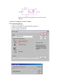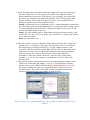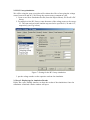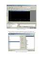
1
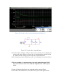
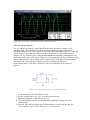
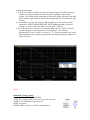
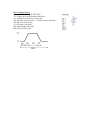
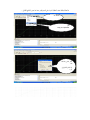
Electronics I LAB Lab 1: Lab 1 : Introduction to PsPise 1-Introduction to PsPise : SPICE (Simulation Program for Integrated Circuits Emphasis.) is a po werful general purpo se analog and mixed- mode circuit simulator that is used to .verify circuit designs and to predict the circuit behavior. PSpice is a PC version of SPICE (which is currently available from OrCAD Corp. Capture : is used to drawn a circuit on the screen, known formally as schematic capture. It offers great flexibility compared with a traditional pencil and paper drawing, as design changes can be incorporated and errors corrected quickly and easily. (On the other hand, it is much faster to de velop the outline of a circuit using pe ncil and paper.) PSpice : simulates the captured circuit. You can analyse its behaviour in many ways and confirm that it performs as specified. PCB Editor : Is used to design printed circuit boards. Analys es you can run with PSpice > DC sweep & AC calculations These DC analyses evaluate circuit performance in response to a direct current source. These AC analyses evaluate circuit performance in response to a small-signal alternating source. DC PSpice computes this analysis DC sweep Steady-state voltages and c urrents when sweeping a source, a model parameter, or temperature over a range of values. Bias point Bias point data in addition to what is automatically computed in any detail simulation. AC sweep Small-signal response of the circuit (linearized around the bias point) when sweeping one or more sources over a range of frequencies. Outputs include voltages and currents with magnitude and p hase; you can use this information to obtain Bode plots. Transient Voltages and c urrents tracked o ver time. 2. PSpice with OrCAD Capture Before one can simulate a circuit one needs to specify the circuit configuration. This can be done in a variety of ways. One way is to enter the circuit description as a text file in terms of the elements, connections, the mode ls of the elements and the type of analysis. This file is called the SPICE input file or source file . An alternative way is to use a schematic entry program such as OrCAD CAPTURE. Capture is a user- friendly program that allows you to capture the schematic of the circuits and to specify the type of simulation. Capture is non only intended to generate the input for PSpice but also for PCD layout design programs. The following figure summarizes the different steps involved in simulating a circuit with Capture and PSpice. We'll describe each of these briefly through a couple of examples. Step 1: Circuit Creation with Capture • Create a new Analog, mixed AD project • Place circuit parts • Connec t the parts • Specify values and names Step 2: Specify type of simulation • Create a simulation profile • Select type of analysis: Bias, DC sweep, Transient, AC sweep • Run PSpice Step 3: View the results • Add traces to the probe window • Use cursors to analyze waveforms • Check the output file, if needed • Save or print the results The values of elements can be specified using scaling factors (upper or lower case): T or Tera (= 1E12); G or Giga (= E9); MEG or Mega (= E6); K or Kilo (= E3); M or Milli (= E-3); U or Micro (= E-6); N or Nano (= E-9); P or Pico (= E-12) F of Femto (= E-15) Both upper and lower case letters are allowed in PSpice and HSpice. As an example, one can specify a capacitor of 225 picofarad in the following ways: 225P, 225p, 225pF; 225pFarad; 225E-12; 0.225N Notice that Mega is written as MEG, e.g. a 15 megaOhm resistor can be specified as 15MEG, 15MEGohm, 15meg, or 15E6. Be careful not to use M for Mega! When you write 15Mohm or 15M, Spice will read this as 15 milliOhm! We'll illustrate the different types of simulations for the following circuit: Figure 2: Circuit to be simulated (screen shot from OrCAD Capture). 2.1 Step 1: Creating the circuit in Capture 2.1.1 Create new project: 1. Open OrCAD Capture 2. Create a new Project: FILE MENU/NEW_PROJECT 3. Enter the name of the project 4. Select Analog or Mixed-AD 5. When the Create PSpice Project box opens, select "Create Blank Project". A new page will open in the Project Design Manager as shown below. Figure 3: Design manager with schematic window and toolbars (OrCAD screen capture) 2.1.2. P lace the components and connect the parts 1. Click on the Schematic window in Capture. 2. To Place a part go to PLACE/PART menu or click on the Place Part Icon. This will open a dialog box shown below. Figure 4: Place Part window 3. Select the library that contains the required components. Type the beginning of the name in the Part box. The part list will scroll to the components whose name contains the same letters. If the library is not available, you need to add the library, by clicking on the Add Library button. This will bring up the Add Library window. Select the desired library. For Spice you should select the libraries from the Capture/Library/PSpice folder. Analog : contains the passive components (R,L,C), mutual inductane, transmission line, a nd voltage and c urrent depe nde nt sources (voltage depe nde nt voltage source E, c urrent-depe nde nt current source F, voltage-dependent current source G and current-dependent voltage source H). Source : give the different type of indepe nde nt voltage and c urrent sources, s uch as Vdc, Idc, Vac, Iac, Vsin, Vexp, pulse, piecewise linear, etc. Browse the libr ary to see what is available. Diode: provides diodes (D…), 4. Place the resistors, capacitor (from the Analog library), and the DC voltage and current source. You can place the part by the left mouse click. You can rotate the components by clicking on the R key. To place another instance of the same part, click the left mouse button again. Hit the ESC key when done with a particular element. You can add initial conditions to the capacitor. Doubleclick on the part; this will open the Property window that looks like a spreadsheet. Under the column, labeled IC, enter the value of the initial condition, e.g. 2V. For our example we assume that IC was 0V (this is the default value). 5. After placing a ll part, you need to place the Ground terminal by clicking o n the GND icon (on the right side toolbar – see Fig. 3 ). W hen the Place Ground window opens, select GND/CAPSYM and give it the name 0 (i.e. ze ro). Do not for get to c hange the name to 0, o therwise PSpice will give an error or "Floating Node". The reason is that SPICE needs a ground terminal as the reference node that has the node number or name 0 (zero). Figure 5: Place the ground terminal box; the ground terminal should have the name 0 6. Now connect the elements using the Place Wire command from the menu (PLACE/WIRE) or by clicking on the Place Wire icon. 7. You can assign names to nets or nodes using the Place Net Alias command (PLACE/NET ALIAS menu). We will do this for the output node and input node. Name these Out and In, as shown in Figure 2. 2.1.3. Assign Values and Names to the parts 1. C hange the va lues of the resistor s by do uble-clicking on the numbe r next to the resistor. You can also change the name of the resistor. Do the same for the capacitor and voltage and c urrent source. 2. I f you haven't done so yet, you can assign na mes to node s (e.g. Out and I n nodes). 3. Save the project 2.2 Step 2: Specifying the type of analysis and simulation As mentioned in the introduction, Spice allows you do to a DC bias, DC Sweep, Transient with Fourier analysis, AC analysis, Parameter sweep and Temperature sweep. We will first explain how to do the Bias and DC Sweep on the circuit of Figure 2. 2.2.1 BIAS or DC analysis 1. With the schematic open, go to the PSPICE menu and choose NEW SIMULATION PROFILE. 2. In the Name text box, type a descriptive name, e.g. Bias 3. From the Inherit From List: select none and click Create. 4. When the Simulation Setting window opens, for the Analyis Type, choose Bias Point and click OK. 5. Now you are ready to run the simulation: PSPICE/RUN 6. A window will open, letting you know if the simulation was successful. If there are errors, consult the Simulation Output file. 7. To see the result of the DC bias point simulation, you can ope n the Simulation Output file or go back to the schematic and click on the V icon (Enable Bias Voltage Display) and I icon (current display) to s how the voltage and c urrents (see Figure 6). Figure 6: Results of the Bias simulationxt+0 displayed o n the schematic. 2.2.2 DC Sweep simulation We will be using the same circuit but will evaluate the effect of sweeping the voltage source between 0 and 20V. We'll keep the current source constant at 1mA. 1. Create a new New Simulation Profile (from the PSpice Menu); We'll call it DC Sweep 2. For analysis select DC Sweep; enter the name of the voltage source to be swept: V1. The start and end values and the step need to be specified: 0, 20 and 0.1V, respectively (see Fig. below). Figure 7: Setting for the DC Sweep simulation. 3. put the voltage marker on the capacitor and r un the simulation 2.3 S tep 3: Display ing the simulation Results PSpice has a user-friendly interface to show the results of the simulations. Once the simulation is finished a Probe window will ope n. Figure 8: Probe window 1. F rom the TRACE menu select ADD TRACE and select the voltages and current you like to display. In our case we'll add V(out) and V(in). C lick OK. Figure 9: Add Traces window 2. You can also add traces using the "Voltage Markers" in the schematic. From the PSPICE menu select MARKERS/VOLTAGE LEVELS. Place the makers on the Out and In node. When done, right click and select End Mode. Figure 10: Using Voltage Markers to show the simulation result of V(out) and V(in) 3. Go to back to PSpice. You will notice that the waveforms will appear. 4. You can add a second Y Axis and use this to display e.g. the current in Resistor R2, a s shown below. Go to PLOT/Add Y Axis. Next, add the trace for I(R2). 5. You can also use the cursor s on the graphs for Vout and Vin to d isplay the actual values at certain points. Go to TRACE/CURSORS/DISPLAY 6. The cursors will be associated with the first trace, as indicated by the small small rectangle around the legend for V(out) at the bottom of the window. Left click on the first trace. The value of the x and y axes are displayed in the Probe windo w. W hen you right click o n V(out) the va lue of the second cursor will be give n together with the difference between the first and second c ursor. 7. To place the second cursor on the second trace (for V(in)), right click the legend for V(in). You'll notice the outline around V(in) at the bottom of the windo w. W hen you right click the second trace the cursor will snap to it. The values of the first and second cursor will be shown in Probe window. 8. You can chance the X and Y axes by do uble clicking o n them. 9. When adding traces you can perform mathematical calculations on the traces, as indicated in the Add Trace Window to the right of Figure 9. Figure 11: Result of the DC sweep, showing Vout, Vin and the current through resistor R2. Cursors were used for V(out) and V(in). 2.4 Other types of Analysis 2.4.1 Transient Analysis We'll be using the same circuit as for the DC sweep, except that we'll apply the voltage and current sources by closing a switch, as shown in Figure 12. Figure 12: Circuit used for the transient simulation. 1. Insert the SW_tCLOSE switch from the anl_misc.olb Library as shown abo ve. Double click o n the switch TCLOSE value and e nter the va lue when the switch closes. Lets make TCLOSE = 5 ms. 2. S et up the Transient Analys is: go to the PSPICE/NEW SIMULATION PROFILE. 3. Give it a name (e.g. Transient). When the Simulation Settings window opens, select "Time Domain (Transient)" Analysis. Enter also the Run Time. Lets make it 50 ms. For the Max Step size, you can leave it blank or enter 10us. 4. Run PSpice. Figure 13: Results of the transient simulation of Figure 12. Figure 15: Circuit with a sinusoidal input. 5. A Probe window in PSpice will open. You can now add the traces to display the results. In the figure below we plotted the current through the capacitor in the top window and the voltage over the capacitor on the bottom one. 6. After doing the transient simulation results can be displayed as was done before 7. The last example of a transient analysis is with a sinusoidal signal VSIN. The circuit is shown below. We made the amplitude 10V and frequency 10 Hz. 8. Create a Simulation Profiler for the transient analysis and run PSpice. 9. The result of the simulation for Vout and Vin are given in the figure below. Figure 16: Transient simulation with a s inusoidal input 2.4.2 AC Sweep Analysis The AC analys is will app ly a sinusoida l voltage whose frequency is swept over a specified range. The simulation calculates the corresponding voltage and current amplitude and p hases for each frequency. W hen the input amplitude is set to 1 V, the n the output voltage is basically the transfer function. In contrast to a sinusoidal transient analysis, the AC analysis is not a time domain simulation but rather a simulation of the sinusoidal steady state of the circuit. When the circuit contains non- linear element such as diodes and transistors, the elements will be replaced their small-signa l mod els with the parameter values calculated according to the corresponding biasing point. In the first example, we'll show a simple RC filter corresponding to the circuit of Figure 17. Figure 17: Circuit for the AC s weep simulation. 1. Create a new project and build the circuit 2. For the voltage source use VAC from the Sources library. 3. Make the amplitude of the input source 1V. 4. Create a Simulation Profile. In the Simulation Settings window, select AC Sweep/Noise. 5. Enter the start and end frequencies and the number of points per decade. For our example we use 0.1Hz, 10 kHz and 11, respectively. 6. Run the simulation 7. In the Probe window, add the traces for the input voltage. We added a second windo w to d isplay the phase in addition to the magnitude of the output voltage. The voltage can be displayed in dB by specifying Vdb (out) in the Add Trace window (type Vdb(out) in the Trace Expression box. For the phase, type VP(out). 8. A n alternative to s how the voltage in dB and phase is to use marke rs on the schematics: PSPICE/MARKERS/ADVANCED/dBMagnitude or Phase of Voltage, or current. Place the markers on the node of interest. 9. We used the cursors in Figure 18 to find the 3dB point. The value is 6.49 Hz corresponding to a time constant of 25 ms (R1||R2.C). At 10 Hz the attenuation of Vout is 11.4db or a factor of 3.72. This corresponds to the value of the amplitude of the output voltage obtained during the transient analysis of Figure 16 above. Notes: Sinusoidal Voltage Source Vsin (VOFF VAMPL FREQ PHASE) VOFF: DC Voltage offset; set to zero for purely sinewave VAMPL: The amplitude of the sinewave FREQ: Frequency PHASE: Phase in degrees; default value 0 degrees Pulse Voltage Source Vpulse (V1 V2 TD TR TF PW PER) V1: Voltage level at the bottom of the pulse V2: Voltage level at the top o f the pulse TD: The time delay between t = 0 and the start of the pulse TR: Rise time of the pulse TF: Fall time of the pulse PW: Pulsewidth of the pulse PER: Period of the pulse ﻣﻼﺣﻈﺔ ﻳﻤﻜﻨﻚ ﺗﺠﻨﺐ ﺍﻟﺨﻠﻔﻴﺔ ﺍﻟﺴﻮﺩﺍء ﻓﻲ ﺍﻟﺴﻤﻴﻮﻟﻴﺸﻦ ﻋﻨﺪ ﺍﺧﺬ ﺻﻮﺭ ﻟﻠﻨﺘﺎﺋﺞ ﻛﺎﻟﺘﺎﻟﻲ : ﻧﻀﻐﻂ ﻫﻨﺎ ﺍﺧﺘﺮ copy to clipboard ﺍﺧﺘﺮ ﺍﻟﺘﺎﻟﻲ ﻭﺍﺿﻐﻂ ok ﺛﻢ ﺍﻟﺼﻖ ﺍﻟﻨﺘﺎﺋﺞ ﻓﻲ ﺍﻟﻮﺭﺩ References : 1 : PSPICE A brief primer : University of Pennsylvania Department of Electrical and Systems Engineering . 2.PSpice User’s manual, OrCAD Corp. (Cadence Design Systems, Inc.)