1
User Manual
CG635
2.05 GHz Synthesized Clock Generator
Revision 1.3 (08/2010)
Certification
Stanford Research Systems certifies that this product met its published specifications at the time
of shipment.
Warranty
This Stanford Research Systems product is warranted against defects in materials and
workmanship for a period of one (1) year from the date of shipment.
Service
For warranty service or repair, this product must be returned to a Stanford Research Systems
authorized service facility. Contact Stanford Research Systems or an authorized representative
before returning this product for repair.
Information in this document is subject to change without notice.
Copyright © Stanford Research Systems, Inc., 2005. All rights reserved.
Stanford Research Systems, Inc.
1290-C Reamwood Avenue
Sunnyvale, California 94089
Phone: (408) 744-9040
Fax: (408) 744-9049
www.thinkSRS.com
Printed in U.S.A.
CG635 Synthesized Clock Generator
Contents
i
Contents
Contents
i
Safety and Preparation for Use
v
Specifications
vii
Quick Start Instructions
xi
Introduction
Feature Overview
Front-Panel Overview
Outputs
Output Levels
Display
Entry
Modify
Clock Status and Interface Indicators
Rear-Panel Overview
AC Power
GPIB
RS-232
Chassis Ground
Timebase
Tmod Input
Clock Output
PRBS and Clock Option
Operation
1
1
2
2
3
4
4
6
7
8
8
8
9
9
9
9
10
11
13
Front-Panel User Interface
Power On
Displaying a Parameter
Changing a Parameter
Stepping a Parameter
Step Sizes of Exact Factors of Ten
Changing Units
Store and Recall Settings
Secondary Functions
Q and Q̄ Outputs
13
13
13
14
14
14
15
15
15
16
CMOS Output
17
Frequency
Phase
19
20
Secondary Functions
RUN, STOP, TOGGLE
INIT
22
22
22
CG635 Synthesized Clock Generator
Contents
STATUS
PRBS ON/OFF
FREQ/2, FREQx2
REL θ = 0
θ + 90°
GPIB
ADDRS
RS-232
DATA
Factory Default Settings
22
24
24
24
24
24
25
25
25
25
Troubleshooting
26
CG635 Remote Programming
29
Introduction
GPIB
RS-232
Front-Panel Indicators
Command Syntax
29
29
29
29
30
Index of Commands
Instrument Control Commands
Interface Commands
Status Reporting Commands
31
31
31
31
Instrument Control Commands
32
Interface Commands
Status Reporting Commands
36
38
Status Byte Definitions
Serial Poll Status Byte
Standard Event Status Register
Communication Error Status Register
Instrument Status Register
PLL Lock Status Register
Error Codes
40
40
41
41
41
42
43
Performance Evaluation
ii
47
Overview
Equipment Required
CG635 Self Test
47
47
47
Output Level Tests
Q/Q̄ Level Tests
CMOS Level Tests
Transition Time Measurements
48
48
49
50
Frequency Synthesis Tests
Functional Tests
Time Modulation Test
52
53
55
CG635 Synthesized Clock Generator
Contents
Phase Noise Tests
Jitter Tests
iii
56
58
Timebase Calibration
Timebase Calibration Test
Calibration
59
60
60
Circuit Description
61
Overview
Accuracy
Resolution
Phase Noise
61
61
61
61
Circuit Block Diagram
Timebase
Reference Synthesizer
Reference Synthesizer Clean-up
Time Modulation
RF Synthesizer
Programmable Dividers and Clock Fan-out
Determining Register Values
Phase adjustment
Detailed Circuit Description
Timebase
DDS and the 19.40/19.44 MHz Reference
Time Modulation
RF Synthesizer
ECL Dividers and Clock Multiplexer
Microcontroller
Rear-Panel RJ-45 Outputs
RS-232 and GPIB Interfaces
Power Supply Interface
Front-Panel Output Drivers
Front-Panel Q and Q̄ Drivers
Front-Panel CMOS Driver
Front-Panel Display and Keypad
Power Supply
Timebase Options
Optional PRBS Generator
Line Receiver Accessories
62
62
62
63
63
63
64
64
67
69
69
71
73
74
75
76
82
83
83
83
84
84
85
85
86
86
87
CG635 Synthesized Clock Generator
Contents
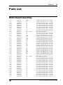
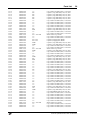
Parts List
iv
93
Motherboard Assembly
Output Driver Assembly
93
102
Power Supply Assembly
106
Chassis and Front-Panel Assembly
107
Option 1 Assembly
Option 2 Assembly
109
111
Option 3 Assembly
111
Schematics
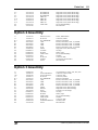
CG635 Schematic Diagram List
113
113
CG635 Synthesized Clock Generator
Safety and Preparation for Use
v
Safety and Preparation for Use
Line Voltage
The CG635 operates from a 90 to 132 VAC or 175 to 264 VAC power source having a
line frequency between 47 and 63 Hz. Power consumption is less than 80 VA total. In
standby mode, power is turned off to the main board. However, power is maintained at all
times to any optional timebases installed. Thus, a unit with an optional rubidium or
ovenized quartz oscillator is expected to consume less than 25 VA and 15 VA of power,
respectively, in standby mode.
Power Entry Module
A power entry module, labeled AC POWER on the back panel of the CG635, provides
connection to the power source and to a protective ground.
Power Cord
The CG635 package includes a detachable, three-wire power cord for connection to the
power source and protective ground.
The exposed metal parts of the box are connected to the power ground to protect against
electrical shock. Always use an outlet which has a properly connected protective ground.
Consult with an electrician if necessary.
Grounding
A chassis grounding lug is available on the back panel of the CG635. Connect a heavy
duty ground wire, #12AWG or larger, from the chassis ground lug directly to a facility
earth ground to provide additional protection against electrical shock.
BNC shields are connected to the chassis ground and the AC power source ground via the
power cord. Do not apply any voltage to the shield.
Line Fuse
The line fuse is internal to the instrument and may not be serviced by the user.
Operate Only with Covers in Place
To avoid personal injury, do not remove the product covers or panels. Do not operate the
product without all covers and panels in place.
Serviceable Parts
The CG635 does not include any user serviceable parts inside. Refer service to a
qualified technician.
CG635 Synthesized Clock Generator
Safety and Preparation for Use
vi
Symbols you may Find on SRS Products
Symbol
Description
Alternating current
Caution - risk of electric shock
Frame or chassis terminal
Caution - refer to accompanying documents
Earth (ground) terminal
Battery
Fuse
On (supply)
Off (supply)
CG635 Synthesized Clock Generator
Specifications
vii
Specifications
Frequency
Range
Resolution
f < 10 kHz
f ≥ 10 kHz
Accuracy
Settling time
1 µHz to 2.05 GHz
1 pHz
16 digits
∆f < ± (2×10-19 + timebase error) × f
<30 ms
Timebase (+20 °C to +30 °C ambient)
Stability
Std. timebase
Opt. 02 (OCXO)
Opt. 03 (Rb)
Aging
Std. timebase
Opt. 02 (OCXO)
Opt. 03 (Rb)
External Input
Output
<5 ppm
<0.01 ppm
<0.0001 ppm
<5 ppm/year
<0.2 ppm/year
<0.0005 ppm/year
10 MHz ± 10 ppm, sine >0.5 Vpp, 1 kΩ impedance
10 MHz, 1.41 Vpp sine (+7 dBm) into 50 Ω
Noise & Spurs
Phase noise (at 622.08 MHz)
100 Hz offset
<–90 dBc/Hz
1 kHz offset
<–100 dBc/Hz
10 kHz offset
<–100 dBc/Hz
100 kHz offset
<–110 dBc/Hz
Phase noise vs. freq.
6 dB/oct. relative to 622.08 MHz
Spurious
<–70 dBc (within 50 kHz of carrier)
Jitter and Wander
Jitter (rms)
Wander (p-p)
<1 ps (1 kHz to 5 MHz bandwidth)
<20 ps (10 s persistence)
Time Modulation
Rear-panel input
Sensitivity
Range
Bandwidth
BNC, DC coupled, 1 kΩ
1 ns/V, ±5 %
±5 ns
DC to greater than 10 kHz
CG635 Synthesized Clock Generator
Specifications
viii
Phase
Range
Resolution
Maximum step size
Slew time (∆p > 0°)
±720°
<20 ps
±360°
<300 ms
Q and Q̄ Outputs
Outputs
Frequency range
High level
Amplitude
Level resolution
Level error
Transition time
Symmetry
Source impedance
Load impedance
Pre-programmed levels
Protection
Front-panel BNC connectors
DC to 2.05 GHz
–2.00 V ≤ VHIGH ≤ +5.00 V
200 mV ≤ VAMPL ≤ 1.00 V (VAMPL ≡ VHIGH – VLOW)
10 mV
<1 % + 10 mV
<100 ps (20 % to 80 %)
<100 ps departure from nominal 50 %
50 Ω (±1 %)
50 Ω to ground on both outputs
+5.0 V PECL, +3.3 V PECL, LVDS, +7 dBm, ECL
Continuous to ground, momentary to +5 VDC
CMOS Output
Output
Frequency range
Low level
Amplitude range
Level resolution
Level error
Transition time
Symmetry
Source impedance
Load impedance
Attenuation (50 Ω load)
Preprogrammed levels
Protection
Front-panel BNC
DC to 250 MHz
-1.00 V ≤ VLOW ≤ +1.00 V
500 mV ≤ VAMPL ≤ 6.00 V (VAMPL ≡ VHIGH – VLOW)
10 mV
<2 % of VAMPL + 20 mV
<1.0 ns (10 % to 90 %, with 12pF load at far end of 50 Ω cable)
<500 ps departure from nominal 50%
50 Ω (reverse terminates cable reflection)
Unterminated 50 Ω cable of any length
Output levels are divided by 2
VLOW = 0; VHIGH = 1.2, 1.8, 2.5, 3.3, or 5.0 V
Continuous to ground, momentary to +5 VDC
RS-485 Output
Output
Frequency range
Clock output
Transition time
Source impedance
Load impedances
Logic levels
Recommended cable
Protection
Rear-panel RJ-45
DC to 105 MHz
Pin 7 and pin 8 drive twisted pair
<800 ps (20% to 80%)
100 Ω between pin 7 and pin 8
100 Ω between pin 7 and pin 8
VLOW = +0.9 V, VHIGH = +2.2 V
Straight-through Category-6
Continuous to ground, momentary to +5 VDC
CG635 Synthesized Clock Generator
Specifications
ix
LVDS Output (EIA/TIA-644)
Output
Frequency range
Clock output
Transition time
Source impedance
Load impedances
Logic levels
Recommended cable
Protection
Rear-panel RJ-45
DC to 2.05 GHz
Pin 1 and pin 2 drive twisted pair
<100 ps (20% to 80%)
100 Ω between pin 1 and pin 2
100 Ω between pin 1 and pin 2
VLOW = +0.96 V, VHIGH = +1.34 V
Straight-through Category-6
Continuous to ground, momentary to +5 V
PRBS (Opt. 01) (EIA/TIA-644)
Frequency range
Level
Outputs
PRBS generator
Transition time
Load impedance
DC to 1.55 GHz
LVDS on rear-panel SMA jacks
PRBS, –PRBS, CLK & –CLK
x7 + x6 + 1 for a length of 27 – 1 bits
<100 ps (20 % to 80 %)
50 Ω to ground on all outputs
Accessory Power (on rear-panel RJ-45 connector)
+5 VDC
–5 VDC
Ground return
Short circuit protection
Polarity clamps
Pin 3
Pin 5
Pin 4 and pin 6
Current limited to 375 mA
Diode clamps prevent polarity inversion
(2 ADC max., 120 A non-rep.)
General
Computer interfaces
Non-volatile memory
Line power
Standby power
Operating power
Dimensions
Weight
Warranty
IEEE-488.2 and RS-232 standard. All instrument functions can be
controlled through the computer interfaces.
Ten sets of instrument configurations can be stored and recalled.
Universal input, 90 to 264 VAC,
47 Hz to 63 Hz
<5 W (std. timebase)
<15 W (opt. 02, OCXO timebase)
<25 W (opt. 03, Rb timebase)
<30 W (std. timebase)
<40 W (opt. 02, OCXO timebase)
<50 W (opt. 03, Rb timebase)
8.5” × 3.5” × 13” (WHD)
<9 lbs.
One year parts and labor on defects in materials and workmanship
CG635 Synthesized Clock Generator
Specifications
x
Optional Receiver Modules
General
Inputs
Outputs
Dimensions
RJ-45. Connects to CG635 via standard Category-6 cable.
Q / Q̄ on SMA connectors
1 5/8” × 1” × 3” (WHD)
Models
Model
Levels
CG640
CG641
CG642
CG643
CG644
CG645
CG646
CG647
CG648
CG649
+5 V CMOS
+3.3 V CMOS
+2.5 V CMOS
+5 V PECL
+3.3 V PECL
+2.5 V PECL
+7 dBm RF
CML/NIM
NEG ECL
LVDS
Notes:
Source
Impedance
50 Ω
50 Ω
50 Ω
50 Ω
50 Ω
50 Ω
50 Ω
50 Ω
50 Ω
50 Ω
Termination
Impedance
High Z
High Z
High Z
High Z
50 Ω
50 Ω
50 Ω
50 Ω
50 Ω
50 Ω
Transition
Time (max)
2.0 ns
800 ps
800 ps
800 ps
100 ps
100 ps
100 ps
100 ps
100 ps
100 ps
Fmax (2)
105 MHz(1)
250 MHz
250 MHz
250 MHz
2.05 GHz
2.05 GHz
2.05 GHz
2.05 GHz
2.05 GHz
2.05 GHz
(1) Output is set to logic ‘0’ above Fmax.
(2) Except for the CG640, all outputs continue to operate above Fmax with reduced amplitude.
Maximum operating frequency is also limited by the CAT-6 cable length. At 2 GHz, cable
lengths up to 10 feet may be used. At 10 MHz, cable lengths of up to 200 feet may be used.
See Figure 3 on page 11 for the maximum recommended cable lengths at other frequencies.
CG635 Synthesized Clock Generator
Quick Start Instructions
xi
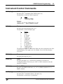
Quick Start Instructions
Step by Step Example
1. With the power button in the Standby position, connect the CG635 to a grounded
outlet using the power cord provided.
2. Push in the power button to turn on the CG635. The CG635 will perform some
start up tests and then recall the instruments’ last known settings from non
volatile memory.
3. Reset the CG635 to its default state by pressing sequentially the following 3 keys
located in the ENTRY section of the front panel: ‘SHIFT’, ‘+/-’, ‘Hz’. This
performs the INIT function which resets the instrument to its default settings.
The INIT function will set the frequency to 10 MHz, set the phase to 0 degrees,
set the output levels for Q and Q̄ to LVDS, set the output levels for CMOS to
3.3 V, and select the frequency for display. The LVDS and +3.3 V LEDs in the
OUTPUT LEVELS section of the front panel should be on. The FREQ LED in
the DISPLAY section should be on. The seven segment display should show
10.000000000 and the MHz LED should be lit. This indicates that the frequency
is 10 MHz.
4. Connect the CMOS output to an oscilloscope with a high impedance input to see
that the output is indeed a 3.3 V square wave with a frequency of 10 MHz.
5. Adjust the frequency to 5 MHz by pressing the following keys sequentially: ‘5’,
‘MHz’. The display should change to 5.000000000 MHz. The oscilloscope
should now display a 5 MHz square wave with amplitude 3.3 V.
6. Adjust the CMOS output up to 5.0 V by pressing the CMOS ▲ key in the
OUTPUT LEVELS section of the front panel. The +3.3 V LED should turn off
and the +5.0 V LED should turn on. The oscilloscope should now display a
5 MHz square wave with amplitude 5.0 V.
7. Press the ‘CMOS HIGH’ key in the DISPLAY section of the front panel. The
CMOS HIGH LED should turn on and the seven segment display should show
5.00 VDC.
8. Adjust the CMOS output to 4.5 V by pressing the following keys sequentially in
the ENTRY section of the front panel: ‘4’, ‘.’, ‘5’, ‘VOLT’. The seven segment
display should now show 4.50 VDC. In the OUTPUT LEVELS section, the
+5.0 V and VAR LEDs should be lit. This indicates that the current CMOS
output voltage varies from, but is closest to the +5.0 V standard output level.
9. Press the CMOS ▼ key in the OUTPUT LEVELS section of the front panel. The
CMOS output changes to the nearest standard level in the direction of the
indicated key, which is 3.3 V in this case. The VAR LED should turn off,
indicating that the current output is at a standard level.
CG635 Synthesized Clock Generator
Quick Start Instructions
xii
10. Press the ‘FREQ’ key in the DISPLAY section to display the current frequency.
The seven segment display should show 5.000000000 MHz.
11. Press the ‘STEP SIZE’ key in the MODIFY section of the front panel. The
display should now show 1.000 Hz, and the STEP LED should be lit. This
indicates that the current step size for frequency is 1.000 Hz.
12. Change the frequency step size to 1 kHz by pressing the following keys
sequentially in the ENTRY section of the front panel: ‘1’, ‘kHz’. The display
should now show 1.000000 kHz.
13. Switch back to the frequency display be pressing the ‘STEP SIZE’ key again.
The STEP LED should turn off, and the display should show the current
frequency of 5.000000000 MHz. The digit corresponding to 1 kHz should be
blinking, indicating that frequency steps will change that digit by one.
14. Step the frequency up by 1 kHz by pressing the MODIFY ▲ key. The frequency
should now display 5.001000000 MHz.
15. For more details about the operation of keys on the front panel, see the Front
Panel Overview (page 2) in the Introduction.
16. For more details about a particular feature, see the chapter Operation (page 13).
CG635 Synthesized Clock Generator
Introduction
1
Introduction
Feature Overview
The CG635 Synthesized Clock Generator provides precise, low-jitter digital clock signals
for applications ranging from the development of digital circuits to the testing of
communications networks.
The CG635 generates single ended and differential clocks from 1 µHz to 2.05 GHz with
sub-picosecond jitter. Clock frequencies may be set with up to 1 pHz resolution and
16 significant digits. Front-panel outputs have continuously adjustable offsets and
amplitudes, and may be set to standard logic levels including CMOS, PECL, ECL, and
LVDS. A rear-panel output delivers clocks at RS-485 and LVDS over twisted pairs.
Several instrument features support more complex tasks. The phase of the outputs may be
adjusted with nanodegree resolution at 2 Hz, and one-degree resolution at 2 GHz. The
timing of clock edges may be modulated over ±5 ns by an external analog signal. An
optional pseudo-random binary sequence (PRBS) generator (Opt. 01) provides clock and
data outputs at LVDS levels for eye-pattern testing of serial data channels. Edge
transition times are typically 80 ps.
The standard crystal oscillator timebase of the CG635 provides sufficient accuracy for
many applications. An optional ovenized crystal oscillator (Opt. 02), or rubidium
frequency standard (Opt. 03), may be added to improve frequency stability and reduce
aging. The CG635 may also be locked to an external 10 MHz timebase.
The CG635 delivers a low spurious output signal—better than most commercial
synthesizers. Phase noise for a 622.08 MHz carrier at 100 Hz offset is less than
–80 dBc/Hz, and the spurious response is better than –70 dBc.
All instrument functions may be controlled from the front panel or via the GPIB (IEEE488.2) or RS-232 interfaces. Up to ten complete instrument configurations can be stored
in non-volatile memory and recalled at any time. A universal input AC power supply
allows world-wide operation.
Several clock receiver modules are available which may be connected to the rear-panel
RS-485/LVDS output via Category-6 cable. These accessories provide complementary
high-speed transitions at standard logic levels on SMA connectors, and may be located at
a substantial distance from the instrument. CMOS (+5 V, +3.3 V, and +2.5 V), PECL
(+5 V, +3.3 V and +2.5 V), RF (+7 dBm), CML/NIM, ECL, and LVDS outputs are all
available.
CG635 Synthesized Clock Generator
Introduction
2
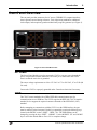
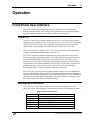
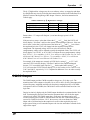
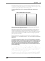
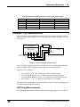
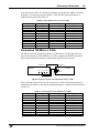
Front-Panel Overview
The front panel was designed to provide a simple, intuitive, user interface to all the
CG635 features (see Figure 1). The power switch is located in the lower right corner of
the front panel. Pushing the switch enables power to the instrument. Pushing the switch
again places the instrument in stand-by mode, where power is enabled only to optionally
installed timebases. Power to the main board is turned off in stand-by mode.
The front panel provides three output drivers for connecting the CG635 clock signals to
user applications via standard BNC cables. The two upper outputs are complementary,
high-speed, ECL compatible output drivers. The lower output is a CMOS output driver.
Keys on the front panel are divided into four sections to indicate their overall
functionality: OUTPUT LEVELS, DISPLAY, ENTRY, and MODIFY. Keys in the
OUTPUT LEVELS section modify the amplitude and offset of the clock signals provided
by the front panel output drivers. Keys in the DISPLAY section control what is shown in
the main display. The user can choose among six standard displays. Keys in the ENTRY
section are used for changing the currently displayed item to a specific value. This
section is also used to access secondary functions. Keys in the MODIFY section allow
the user to increment the currently displayed item by configurable steps.
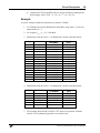
Figure 1: The CG635 Front Panel
Outputs
Q and Q̄
The CG635 front panel includes three BNC outputs. The upper two outputs, labeled Q
and Q̄, are high-speed drivers that operate from DC to 2.05 GHZ. The outputs provide the
user with fast, complementary voltages at the selected frequency, amplitude, and offset.
CG635 Synthesized Clock Generator
Introduction
3
To operate at specification, BOTH outputs should be terminated into 50 Ω, even if only
one output is used.
CMOS
The bottom output driver is a CMOS compatible driver that can operate from DC to
250 MHz. It drives the output at the selected frequency, amplitude and offset. At
frequencies above 250 MHz, the CMOS driver will be turned off and forced to a low
logic state. To operate at specification, the CMOS output driver should be terminated into
a high impedance input and NOT terminated into 50 Ω.
Output Levels
Standard Levels
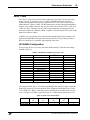
The CG635 provides a simple method for switching among five standard voltage levels
for the Q / Q̄ and CMOS outputs. The meaning of the five standard levels is summarized
in Table 1 and Table 2 below:
Table 1: Q / Q̄ Standard Output Levels
Label
PECL5V
PECL3.3V
LVDS
+7 dBm
ECL
Description
ECL run on +5 VDC supply
ECL run on +3.3 VDC supply
Low voltage differential signaling
1 Vpp with 0.0 VDC offset
ECL run on negative supply
VHIGH (V)
4.00
2.30
1.43
0.50
–1.00
VLOW (V)
3.20
1.50
1.07
–0.50
–1.80
Table 2: CMOS Standard Output Levels
Label
+5.0V
+3.3V
+2.5V
+1.8V
+1.2V
Description
5 V CMOS
3.3 V CMOS
2.5 V CMOS
1.8 V CMOS
1.2 V CMOS
VHIGH (V)
5.00
3.30
2.50
1.80
1.20
VLOW (V)
0.00
0.00
0.00
0.00
0.00
VHIGH and VLOW indicate the voltage driven by the Q / Q̄ or CMOS outputs for the high
and low logic levels.
LEDs in the OUTPUT LEVELS section indicate the standard level that is currently being
driven on the output. Pressing the ▲ and ▼ keys in this section will move the standard
output level up and down in the table, respectively.
Variable Levels
A sixth LED, labeled VAR, turns on when the current output levels do not correspond to
any of the standard levels. In this case, the standard level LED indicates the standard
level that is closest to the current level. Pressing the ▲ and ▼ keys when the VAR LED
is on, forces the output to the closest standard output in the direction indicated by the key.
CG635 Synthesized Clock Generator
Introduction
4
Display
The DISPLAY section allows the user to select which values are reported in the main
front panel display. The LEDs in the display section indicate what is currently being
displayed or edited. The meaning of the LEDs and keys are summarized in Table 3.
Table 3: DISPLAY Section Keys
Label
FREQ
PHASE
Q / Q̄ HIGH
Q / Q̄ LOW
CMOS HIGH
CMOS LOW
Value Shown in Main Display When Pressed
Current frequency
Current phase
Voltage for a Q / Q̄ logic high state
Voltage for a Q / Q̄ logic low state
Voltage for a CMOS logic high state
Voltage for a CMOS logic low state
The keys are used to change the main display to the indicated item. Pressing ‘FREQ’, for
example, will cause the CG635 to display the current frequency. The FREQ LED will
turn on, indicating that the current display is frequency.
Entry
Numeric Entry
The ENTRY section is used to modify the current settings of the CG635. In most cases,
the currently displayed item can be changed by entering a new value with the numeric
keys, and pressing an appropriate units key to complete the entry. For example, if the
frequency is currently being displayed, pressing the keys ‘1’, ‘MHz’, sequentially will
change the frequency to 1 MHz. Similarly, if the CMOS HIGH voltage is displayed,
pressing the keys ‘2’, ‘.’, ‘1’, ‘VOLT’ will set the CMOS logic high voltage to 2.1 VDC.
Store and Recall Settings
The ‘STO’ and ‘RCL’ keys are for storing and recalling instrument settings, respectively.
The instrument saves the frequency, phase, Q / Q̄ and CMOS output levels, all the
associated step sizes, the run/stop state, the PRBS state, and the current display. Up to ten
different instrument settings may be stored in the locations 0 to 9. To save the current
settings to location 5, press the keys ‘STO’, ‘5’, ‘Hz’, sequentially. To recall instrument
settings from location 5, press the keys ‘RCL’, ‘5’, ‘Hz’ sequentially.
Secondary Functions
Many of the keys have secondary functions associated with them. The names of these
functions are printed above the key. The ‘4’ key, for example, has FREQx2 above it. The
meaning of the secondary functions is summarized in Table 4.
Table 4: Secondary Functions
Label
RUN
STOP
Function Description
Enables the output. Drives the output at the current frequency.
Stops the output. Forces the output to a logic low state.
CG635 Synthesized Clock Generator
Introduction
TOGGLE
INIT
STATUS
PRBS ON
PRBS OFF
FREQ/2
FREQx2
REL θ = 0
θ + 90°
GPIB
ADDRS
RS-232
DATA
←
→
5
When stopped, toggles the logic state of the output
Resets the instrument to its default settings
Displays instrument status
If installed, turns on the pseudo-random binary generator
If installed, turns off the pseudo-random binary generator
Divides the current frequency by 2 and displays frequency
Multiplies the current frequency by 2 and displays frequency
Defines the current phase to be 0 degrees and displays phase
Increments the phase by 90 degrees and displays phase
Enables the GPIB remote interface. Disables RS-232.
Displays / Sets the GPIB primary address for the CG635
Enables the RS-232 remote interface. Disables GPIB.
Displays the most recent data received over the remote interface
Increases the current step size by the next exact factor of ten
(Located in the MODIFY section.)
Decrease the current step size by the next exact factor of ten
(Located in the MODIFY section.)
A more detailed description of each of the secondary functions is given in the Secondary
Functions section of the Operation chapter (page 22).
The secondary functions can only be accessed when SHIFT mode is active, which is
indicated by the SHIFT LED being turned on. The SHIFT mode can be toggled on and
off by pressing the ‘SHIFT’ key. Therefore, to increase the frequency by a factor of four,
you would press the ‘SHIFT’ key to activate SHIFT mode, and then press ‘4’ twice to
execute FREQx2 twice. Pressing ‘SHIFT’ again toggles SHIFT mode off.
Most of the secondary functions will automatically toggle SHIFT mode off when
executed. FREQ/2, FREQx2, θ + 90°, and TOGGLE are exceptions to this rule. This
allows the user to easily sweep frequency or phase without having to continually
reactivate SHIFT mode.
Secondary functions that have an arrow ( ) printed after them, such as INIT, GPIB,
ADDRS, and RS-232, require that the user press the key ‘Hz’ to complete the action. For
example, to initialize the instrument to its default settings, you would sequentially press
‘SHIFT’, ‘INIT’, ‘Hz’.
Cancel
The ‘SHIFT’ key also functions as a general purpose CANCEL key. Any numeric entry
which has not been completed by pressing a units key, can be canceled by pressing the
‘SHIFT’ key. Because of the dual role played by the SHIFT key, the user may have to
press ‘SHIFT’ twice to reactivate SHIFT mode. The first key press cancels the current
action, and the second key press activates SHIFT mode.
CG635 Synthesized Clock Generator
Introduction
6
Modify
Stepping Up and Down
The MODIFY section is used to step the currently displayed item up or down by a
programmed amount. Each of the six standard display items listed in the DISPLAY
section has a step size associated with it. Normally, pressing the MODIFY ▲ and ▼
keys causes the displayed item to increment and decrement, respectively, by the
associated step size.
Step Size
The step size for the current standard display can be viewed by pressing the ‘STEP SIZE’
key. Pressing ‘STEP SIZE’ a second time toggles the view back to the standard display.
When the step size is being viewed, the STEP LED in the main display will be turn on.
To view the frequency step size, press ‘FREQ’, ‘STEP SIZE’, sequentially. Pressing
‘FREQ’ ensures that frequency is the current standard display. Pressing ‘STEP SIZE’
then toggles the main display to the step size associated with frequency.
The step size can be changed in a number of ways. If the current step size is being
displayed, the user can modify the current step size in one of two ways. First, you can
enter a new value with the numeric keys in the ENTRY section and complete the entry by
pressing an appropriate units key. Second, you can increment and decrement the current
step size by exact factors of ten by pressing the MODIFY ▲ and ▼ keys, respectively.
For example, if the currently displayed frequency step size is 1.000 Hz, then the step size
can be increased to 10.000 Hz by pressing MODIFY ▲ once.
The step size can also be changed, even when the current step size is not being displayed.
This is accomplished by accessing the SHIFTED functions ← and → shown above the
MODIFY ▲ and ▼ keys, respectively. For example, pressing ‘SHIFT’, MODIFY ▲,
sequentially will increase the associated step size to the next exact factor of ten.
When the step size of a standard display item is an exact factor of ten, the corresponding
digit in the main display will blink. This provides a convenient visual cue to let the user
know which digit will change when the user presses the MODIFY ▲ and ▼ keys. For
example, if the frequency step size is 1.000 Hz, and the displayed frequency is
123456.789 Hz, then the ‘6’ will be blinking. Pressing the MODIFY ▲ key will step the
frequency up 1 Hz to 123457.789 Hz.
Remote and Local Mode
The REM LED turns on when the CG635 is placed in remote mode by the GPIB bus. In
this mode, all the front panel keys are disabled and the instrument can only be controlled
via the GPIB bus. The user can return to normal, local mode by pressing the ‘STEP
SIZE’ key once. The ‘LOCAL’ label above the key indicates the dual functionality of the
‘STEP SIZE’ key.
CG635 Synthesized Clock Generator
Introduction
7
Clock Status and Interface Indicators
10 MHz & SYNTH
In the upper right portion of the front panel are two groups of LED indicators. The upper
group is labeled 10 MHz & SYNTH. This contains the EXT and UNLK LEDs. The EXT
LED indicates that the CG635 has detected an external 10 MHz reference at the 10 MHz
input BNC on the rear panel of the CG635. The CG635 will lock its internal clock to this
external reference.
The UNLK LED indicates that the output has not yet stabilized for some reason. This is
usually due to a user request to change frequency or phase. Frequency changes can take
roughly 30 ms to stabilize. A backward phase step of 360 degrees at 1 Hz can take as
long as 1.5 s to complete. The UNLK LED may also indicate that the internal clock has
not locked to the external reference.
INTERFACE
The lower group of LED indicators is labeled INTERFACE. These LEDs indicate the
current status of RS-232 or GPIB remote programming interfaces. The RS-232 LED is on
if the instrument is configured to accept commands over the RS-232 interface.
Alternately, the GPIB LED is on if the instrument is configured to accept commands over
the IEEE-488 port. When a character is received or sent over one of the interfaces, the
ACT LED will flash. This is helpful when troubleshooting communications problems. If
a command received over the remote interface fails to execute due to either a parsing
error or an execution error, the ERR LED will flash.
CG635 Synthesized Clock Generator
Introduction
8
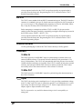
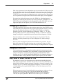
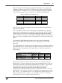
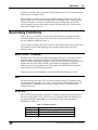
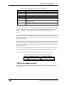
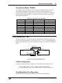
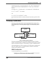
Rear-Panel Overview
The rear panel provides connectors for AC power, GPIB/RS-232 computer interfaces,
chassis ground, external timing references, clock edge timing modulation, additional
clock outputs, and an optional, pseudo-random binary sequence generator (see Figure 2).
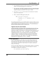
Figure 2: The CG635 Rear Panel
AC Power
The Power Entry Module is used to connect the CG635 to a power source through the
power cord provided with the instrument. The center pin is connected to the CG635
chassis so that the entire box is grounded.
The source voltage requirements are: 90 to 132 VAC or 175 to 264 VAC, 47 to 63 Hz (80
VA total).
Connect the CG635 to a properly grounded outlet. Consult an electrician if necessary.
GPIB
The CG635 comes standard with a GPIB (IEEE-488) communications port for
communications over a GPIB bus. The CG635 supports the IEEE-488.1 (1978) interface
standard. It also supports the required common commands of the IEEE-488.2 (1987)
standard.
Before attempting to communicate with the CG635 over the GPIB interface, the port
must be enabled via the front panel. Do this by sequentially pressing the following keys
located in the ENTRY section: ‘SHIFT’, ‘GPIB’, ‘Hz’. The GPIB address can be
changed by pressing the keys ‘SHIFT’, ‘ADDRS’. Use the MODIFY ‘UP’ and ‘DOWN’
keys to select the desired address. Press ‘Hz’ to complete change.
CG635 Synthesized Clock Generator
Introduction
9
A host computer interfaced to the CG635 can perform virtually any operation that is
accessible from the front panel. Programming the CG635 is discussed in the CG635
Remote Programming chapter.
RS-232
The CG635 comes standard with an RS-232 communications port. The RS-232 interface
connector is a standard 9 pin, type D, female connector configured as a DCE (transmit on
pin 3, receive on pin 2). The communication parameters are fixed at: 9600 Baud, 8 Data
bits, 1 Stop bit, No Parity, RTS/CTS Hardware Flow Control.
Before attempting to communicate with the CG635 over RS-232, the port must be
enabled via the front panel. Do this by sequentially pressing the following keys located in
the ENTRY section: ‘SHIFT’, ‘RS-232’, ‘Hz’.
A host computer interfaced to the CG635 can perform virtually any operation that is
accessible from the front panel. Programming the CG635 is discussed in the CG635
Remote Programming chapter.
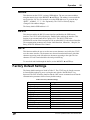
Chassis Ground
Use this grounding lug to connect the CG635 chassis directly to facility ground
Timebase
10 MHz IN
The CG635 provides a 10 MHz BNC input for synchronizing its internal clock to an
external 10 MHz reference. The external reference should provide greater than 0.5 Vpp
into a 1 kΩ impedance. The CG635 will automatically detect the presence of an external
10 MHz reference and lock to it if possible. If the CG635 is unable to lock to the external
reference, the front-panel UNLK LED will turn on and stay on until the CG635 either
successfully locks to the external reference or the reference is removed.
10 MHz OUT
The CG635 provides a 10 MHz BNC output for synchronizing other instrumentation to
the CG635’s timebase.
Tmod Input
The CG635 clock edges can be modulated over ±5 ns by providing a modulation voltage
to the Tmod BNC input. The input is calibrated to provide 1 ns of modulation for 1 volt of
input swing. The input can accept voltages of ±5 V. Positive inputs advance the clock
outputs, negative inputs retard the clock outputs.
The Tmod input can be very useful for characterizing a circuit’s susceptibility to
timing jitter.
CG635 Synthesized Clock Generator
Introduction
10
Clock Output
The CG635 interfaces to a number of optional clock receiver modules which can be used
to get a clock signal from the CG635 to where it is needed. The receiver modules
regenerate the clock locally providing the user with clean, fast clock edges, even if the
CG635 is several meters away. Receiver modules are available for generating most of the
standard CMOS and ECL signal levels.
All modules provide both +CLK and –CLK with a source impedance of 50 Ω, and
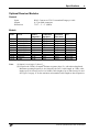
connect to the rear-panel RJ-45 connector using standard Category-6 cable. Table 5
summarizes the features of the optional receiver modules offered by SRS. The maximum
frequency (Fmax) listed in the table for each module is the maximum frequency at which
the module operates at specification. With the exception of the CG640, the modules
continue to operate above Fmax, but with reduced amplitude.
Table 5: Optional Receiver Modules
Model
Description
Termination
Impedance
CG640
CG641
CG642
CG643
CG644
CG645
CG646
CG647
CG648
CG649
CMOS (+5 Vcc)
CMOS (+3.3 Vcc)
CMOS (+2.5 Vcc)
PECL (+5 Vcc)
PECL (+3.3 Vcc)
PECL (+2.5 Vcc)
RF (+7 dBm)
CML/NIM
ECL
LVDS
High Z
High Z
High Z
High Z
50 Ω
50 Ω
50 Ω
50 Ω
50 Ω
50 Ω
Transition
Time(max)
2.0 ns
800 ps
800 ps
800 ps
100 ps
100 ps
100 ps
100 ps
100 ps
100 ps
Fmax (2)
105 MHz (1)
250 MHz
250 MHz
250 MHz
2.05 GHz
2.05 GHz
2.05 GHz
2.05 GHz
2.05 GHz
2.05 GHz
Notes: (1) Output is set to logic ‘0’ above Fmax.
(2) Maximum operating frequency is limited by the CAT-6 cable length.
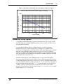
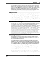
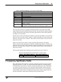
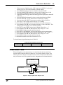
The maximum frequency may also be limited by the CAT-6 cable length. At 2 GHz, the
cable may be up to 10 feet long. At 10 MHz, the cable may be up to 200 feet long.
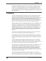
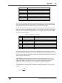
Figure 3 summarizes the limitation on maximum frequency due to cable length.
If clock regeneration is not needed, the user can interface directly to the clock signals
provided on the various pins of the RJ-45 connector. The clock signals and pin
assignments are printed on the rear panel of the CG635 in the CLOCK OUT section.
CG635 Synthesized Clock Generator
Introduction
11
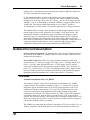
Figure 3: Maximum recommended CAT-6 cable length as a function frequency.
Maximum Recommended CAT-6 Cable Length vs. Frequency
Maximum CAT-6 Cable (meters)
1000
100
10
1
1
10
100
1000
10000
Frequency (MHz)
PRBS and Clock Option
An optional pseudo-random binary sequence generator for the CG635 is also available
from SRS. If installed, both the PRBS data and the clock are output as LVDS levels on
rear-panel SMA connectors.
A Pseudo-Random Binary Sequence (PRBS) generator is used for testing data
transmission systems. A typical arrangement is to display an “eye pattern” on an
oscilloscope by triggering the oscilloscope with the clock while displaying the (random)
data after it passes through the data transmission system. An “open” eye pattern is
necessary for reliable data transmission. The eye pattern “closes” from the left and right
with jitter, and from the top and bottom with insufficient channel bandwidth, increasing
the likelihood for transmission errors.
The most common way to create a PRBS generator is to use a linear shift-register,
feeding the input of the shift-register with the exclusive OR of two (particular) data bits
as they shift through the system. The CG635 uses a 7-bit ECL shift register that provides
a pseudo-random bit sequence which repeats after 27 – 1 = 127 clock cycles. The data bit
stream is described by the polynomial x7 + x6 + 1. It satisfies many criteria to qualify as
“random”; however, it does repeat itself (exactly) after 127 clock cycles. Another
departure from randomness is that the longest string of “1’s” is seven in a row, while the
longest string of “0’s” is six in a row.
CG635 Synthesized Clock Generator
Operation
13
Operation
Front-Panel User Interface
The previous chapter described the function of the front-panel keys based on their
location on the front panel. This section provides guidelines for viewing and changing
instrument parameters independent of their location on the front panel.
Power On
At power on, the CG635 performs a number of self tests to verify that various internal
components are operating correctly. If any of the tests fail, the CG635 will briefly display
“Failed” after the test. In such a case, consult the troubleshooting section later in this
chapter before contacting SRS or an authorized representative to repair the unit.
After the self tests have completed, the CG635 will recall the latest known instrument
settings from nonvolatile memory and be ready for use.
The CG635 continuously monitors front-panel key presses and will save the current
instrument settings to nonvolatile memory after approximately ten seconds of inactivity.
To prevent the nonvolatile memory from wearing out, however, the CG635 will not
automatically save instrument settings that change due to commands executed over the
remote interface. The remote commands *SAV and *RCL can be used to explicitly save
instrument settings over the remote interface, if desired. See the CG635 Remote
Programming chapter for more information about these commands.
The CG635 can be forced to boot up at factory default settings. This is accomplished by
pressing and holding the ‘BACK SPACE’ key during power up, until the initialization is
complete. All instrument parameters will be set back to their default values, including the
enabled remote interface and the GPIB address. See the Default Factory Settings section
later in this chapter for a listing of the default settings.
Displaying a Parameter
The CG635 has six main displays which are activated by pressing the keys in the
DISPLAY section of the front panel. The function of each key is summarized in Table 6.
Table 6: DISPLAY Section Keys
Label
FREQ
PHASE
Q / Q̄ HIGH
Q / Q̄ LOW
CMOS HIGH
CMOS LOW
Value Shown in Main Display When Pressed
Current frequency
Current phase
Voltage for a Q / Q̄ logic high state
Voltage for a Q / Q̄ logic low state
Voltage for a CMOS logic high state
Voltage for a CMOS logic low state
CG635 Synthesized Clock Generator
Operation
14
Each of these parameters has an independent step size associated with it. When one of the
six main displays is active, the associated step size for the parameter can be displayed by
pressing the ‘STEP SIZE’ button in the MODIFY section of the front panel. Pressing the
‘STEP SIZE’ key again toggles the display back to the original parameter. When the step
size for a parameter is displayed, the STEP LED in the main display will be highlighted.
For example, to display the frequency, press the ‘FREQ’ key. Now that frequency is
displayed you can display the frequency step size by pressing the ‘STEP SIZE’ key. The
STEP LED should be highlighted in the main display. Pressing ‘STEP SIZE’ once more
toggles the display back to frequency. The STEP LED should now be off.
Changing a Parameter
To change a parameter, enter a new value using the numeric keys in the ENTRY section
of the front panel, and complete the entry by pressing an appropriate units key. Generally
speaking, only displayed parameters can be changed. For example, to change the
frequency to 10 kHz, press the following keys sequentially: ‘FREQ’, ‘1’, ‘0’, ‘kHz’.
Pressing ‘FREQ’ selects it for display and editing. Pressing ‘1’ initiates the parameter
change. Pressing ‘kHz’ completes the numeric entry and sets the frequency to 10 kHz.
The same techniques can be used to change the step size of a parameter. The only
difference is that the parameter step size must be displayed first, before entering a
new value.
If the user enters extra digits beyond the allowed resolution of a parameter, the extra
digits will be ignored. For example, the phase has a resolution of 1 degree at 1 GHz.
Entering a step size of 2.5 degrees will result in the step size being truncated to 2 degrees.
Stepping a Parameter
The six main parameters can be stepped up and down by their associated step sizes by
respectively pressing the ▲ and ▼ keys in the MODIFY section of the front panel. For
example, if frequency is currently being displayed as 10.000000000 MHz, and the
frequency step size is 1.000 Hz, then pressing MODIFY ▲ will change the frequency to
10.000001000 MHz. Pressing MODIFY ▼ will bring the frequency back to 10 MHz.
Step Sizes of Exact Factors of Ten
If a parameter’s step size is an exact factor of ten, then the corresponding digit in the
main display of the parameter will blink. This provides a visual cue to inform the user of
the digit that will change when the parameter is stepped up or down. For example, if the
frequency step size is 1.000 Hz, and the displayed frequency is 123456.789 Hz, then the
‘6’ will be blinking. Pressing the MODIFY ▲ key will step the frequency up 1 Hz to
123457.789 Hz.
When a parameter step size is being displayed, the user can increase or decrease the step
size to the nearest exact factor of ten by pressing the MODIFY ▲ and ▼ keys,
respectively. For example, if the current frequency step size is being displayed as
1.000 Hz, then pressing MODIFY ▲ will increase to the step size to 10.000 Hz.
CG635 Synthesized Clock Generator
Operation
15
The same behavior can also be achieved even when the current step size is NOT being
displayed. This is accomplished by accessing the SHIFTED functions ← and → shown
above the MODIFY ▲ and ▼ keys, respectively. For example, if the frequency is being
displayed as 123456.789 Hz, and the frequency step size is 1 Hz, then sequentially
pressing ‘SHIFT’, MODIFY ▲ will increase the associated step size to 10 Hz. The ‘6’
will stop blinking and the ‘5’ will start blinking to indicate the new step size.
Changing Units
Frequency has the option of being displayed in units of GHz, MHz, kHz, or Hz. When the
user enters a frequency using the front panel, the CG635 will display the frequency in the
units used to complete the entry. For example, pressing the keys ‘FREQ’, ‘1’, ‘0’, ‘kHz’
sequentially, to change the frequency to 10 kHz, will cause the CG635 to display the
result as 10.000000 kHz. The user can change the displayed units by pressing a different
units key. Continuing with the previous example, if the user presses ‘Hz’, the CG635 will
change the display to 10000.000 Hz.
Store and Recall Settings
The ‘STO’ and ‘RCL’ keys are for storing and recalling instrument settings, respectively.
The instrument saves the frequency, phase, Q / Q̄ and CMOS output levels, all the
associated step sizes, the run/stop state, the PRBS state, and the current display. Up to ten
different instrument settings may be stored in the locations 0 to 9. To save the current
settings to location 5, for example, press the keys ‘STO’, ‘5’, ‘Hz’ sequentially. To recall
instrument settings from location 5, press the keys ‘RCL’, ‘5’, ‘Hz’ sequentially. The
user may also use the MODIFY ▲ and ▼ keys to select the desired location, rather than
enter the location directly with the numeric keys. The CG635 will remember the last
location used for store and recall. To reuse the remembered location, simply skip the
numeric entry when storing or recalling settings. For example, to recall settings from the
remembered location, the user should simply press ‘RCL’, ’Hz.’
Secondary Functions
Most of the keys in the ENTRY section of the front panel have secondary functions
associated with them. The names of these functions are printed above the key. The ‘4’
key, for example, has FREQx2 above it.
The secondary functions can only be accessed when SHIFT mode is active, which is
indicated by the SHIFT LED being turned on. The SHIFT mode can be toggled on and
off by pressing the ‘SHIFT’ key. Therefore, to increase the frequency by a factor of four,
you would press the ‘SHIFT’ key to activate SHIFT mode, and then press ‘4’ twice to
execute FREQx2 twice. Pressing ‘SHIFT’ again toggles SHIFT mode off.
Most of the secondary functions will automatically toggle SHIFT mode off when
executed. FREQ/2, FREQx2, θ + 90°, and TOGGLE are exceptions to this rule. This
allows the user to easily sweep frequency or phase without having to continually
reactivate SHIFT mode.
Secondary functions that have an arrow ( ) printed after them, such as INIT, GPIB,
ADDRS, and RS-232, require that the user press the key ‘Hz’ to complete the action. For
CG635 Synthesized Clock Generator
Operation
16
example, to initialize the instrument to its default settings, you would press ‘SHIFT’,
‘INIT’, ‘Hz’ sequentially.
Detailed descriptions of each of the secondary functions can be found later in this
chapter.
Q and Q̄ Outputs
The Q and Q̄ outputs on the front panel are high-speed, differential, ECL-compatible
drivers that operate from DC to 2.05 GHz with a nominal 50 % duty cycle. The rise and
fall times of these outputs are <100 ps. The outputs provide the user with fast,
complementary voltages at the selected frequency, amplitude, and offset. To operate at
specification, BOTH outputs should be terminated into 50 Ω, even if only one output is
used.
The user can easily switch between five standard output voltage levels by pressing the Q /
Q̄ ▲ and ▼ keys in the OUTPUT LEVELS section of the front panel. When the Q / Q̄
outputs are at a standard level, the appropriate standard level LED will be highlighted.
The meaning of the five standard levels is summarized in Table 7.
Table 7: Q / Q̄ Standard Output Levels
Label
PECL5V
PECL3.3V
LVDS
+7 dBm
ECL
Description
ECL run on +5 VDC supply
ECL run on +3.3 VDC supply
Low voltage differential signaling
1 Vpp with 0.0 VDC offset
ECL run on negative supply
VHIGH (V)
4.00
2.30
1.43
0.50
–1.00
VLOW (V)
3.20
1.50
1.07
–0.50
–1.80
VHIGH and VLOW indicate the voltage driven by the Q and Q̄ outputs for the high and low
logic levels, respectively.
Various ECL logic families have different logic thresholds that may vary with
temperature. The ECL levels in the table above were chosen to lie between the levels for
the 10 k and 100 k ECL logic families when operated at 25 ºC. The differences are small:
at 25 ºC the typical VHIGH for an ECL part run off a negative supply is -0.945 V (for the
10 k series) and –1.020 V (for the 100 k series), while VLOW is –1.745 V (for the 10 k
series) and –1.820 V (for the 100 k series). As seen in Table 7, the CG635 will provide a
VHIGH of –1.00 V and a VLOW of –1.80 V.
The user also has the ability to set the Q / Q̄ outputs to nonstandard levels. When the
outputs differ from the standard levels, the Q / Q̄ VAR LED in the OUTPUT LEVELS
section will turn on. In this case, the highlighted standard LED indicates the standard
level nearest the current output levels. Pressing the Q / Q̄ ▲ and ▼ keys when the VAR
LED is on will force the outputs to the nearest standard level in the direction indicated by
the key.
The voltages for Q / Q̄ high and low states can be viewed in the main display by pressing
‘Q/Q̄ HIGH’ and ‘Q/Q̄ LOW’ keys in the DISPLAY section of the front panel.
CG635 Synthesized Clock Generator
Operation
17
The Q / Q̄ high and low voltages may be set to arbitrary values, or stepped up and down
by configurable step sizes by following the instructions described in the Front-Panel User
Interface section at the beginning of this chapter. However, the limits summarized in
Table 8 apply.
Table 8: Limits for Q / Q̄ High and Low Voltages
Parameter
Q / Q̄ HIGH (VHIGH)
Q / Q̄ LOW (VLOW)
Q / Q̄ Amplitude (VHIGH–VLOW)
Minimum
–2.00 V
–3.00 V
0.20 V
Maximum
5.00 V
4.80 V
1.00 V
Resolution
0.01 V
0.01 V
0.01 V
Beware that a +5 V output will dissipate ½ watt into the target system’s 50 Ω
termination.
If the user tries to enter a value that violates the VHIGH or VLOW limit, the CG635 will
briefly display “Volt Error” and leave the current value unchanged. However, if the user
tries to enter a value that is valid in terms of the limits on VHIGH and VLOW, but violates
the amplitude limit, the CG635 will change both the requested voltage and its
complement. The requested voltage will be set to the desired level, and the
complementary voltage will be adjusted to satisfy the amplitude limits. The CG635 will
briefly display “lo is N.NN” or “hi is N.NN” to indicate the new complementary voltage
level. If VHIGH – VLOW would be > 1.00 V, VLOW will be set 1.00 V below VHIGH or VHIGH
will be set 1.00 V above VLOW. If VHIGH – VLOW would be < 0.20 V, VLOW will be set
0.20 V below VHIGH or VHIGH will be set 0.20 V above VLOW.
For example, if the outputs are currently at LVDS levels, setting VHIGH to 5.5 V will
cause the CG635 to briefly display “Volt Error” and leave the outputs unchanged,
because 5.5 V exceeds the upper limit for VHIGH. On the other hand, setting VHIGH to
5.0 V will cause the CG635 to briefly display “Lo is 4.00” and to set VHIGH and VLOW to
5.00 V and 4.00 V, respectively. VLOW is adjusted in addition to VHIGH in order to satisfy
the amplitude limits.
CMOS Output
The CMOS output provides CMOS compatible voltages at a 50 % duty cycle. The
transition times of this output are less than 1.0 ns (10% to 90%). It drives the output at the
selected frequency, amplitude and offset for frequencies ranging from DC to 250 MHz.
At frequencies above 250 MHz, the CMOS driver will be turned off and forced to a low
logic state.
Despite its relatively high speed, the CMOS output should not be terminated with a 50 Ω
load. Terminating the output will not harm the instrument but it will divide the output
voltage levels in half. The CMOS output has a 50 Ω source impedance and so will
reverse terminate pulses which are reflected back from the user’s (unterminated) target
system. For CMOS levels below 2.50 V, the user may wish to terminate the CMOS
output with a 50 Ω load and set the output levels to twice that required by the user’s
target system. Doing so will somewhat improve the rise time and reduce reflected clocks
edges on the output.
CG635 Synthesized Clock Generator
Operation
18
The user can easily switch between five standard output voltage levels by pressing the
CMOS ▲ and ▼ keys in the OUTPUT LEVELS section of the front panel. When the
CMOS output is at a standard level, the CG635 will highlight the appropriate standard
level LED. The meaning of the five standard levels is summarized in the Table 9.
Table 9: CMOS Standard Output Levels
Label
+5.0V
+3.3V
+2.5V
+1.8V
+1.2V
Description
5 V CMOS
3.3 V CMOS
2.5 V CMOS
1.8 V CMOS
1.2 V CMOS
VHIGH (V)
5.00
3.30
2.50
1.80
1.20
VLOW (V)
0.00
0.00
0.00
0.00
0.00
VHIGH and VLOW indicate the voltage driven by the CMOS output for the high and low
logic levels, respectively.
The user also has the ability to set the CMOS output to nonstandard levels. When the
output differs from the standard levels, the CMOS VAR LED in the OUTPUT LEVELS
section will turn on. In this case, the highlighted standard LED indicates the standard
level nearest the current output level. Pressing the CMOS ▲ and ▼ keys when the VAR
LED is on will force the outputs to the nearest standard level in the direction indicated by
the key.
The voltages for CMOS high and low states can be viewed in the main display by
pressing ‘CMOS HIGH’ and ‘CMOS LOW’ keys in the DISPLAY section of the
front panel.
The CMOS high and low voltages may be set to arbitrary values, or stepped up and down
by configurable step sizes by following the instructions described in the Front-Panel User
Interface section at the beginning of this chapter. However, the limits summarized in
Table 10 apply.
Table 10: Limits for CMOS High and Low Voltages
Parameter
CMOS HIGH (VHIGH)
CMOS LOW (VLOW)
CMOS Amplitude(VHIGH–VLOW)
Minimum
–0.50 V
–1.00 V
0.50 V
Maximum
6.00 V
1.00 V
6.00 V
Resolution
0.01 V
0.01 V
0.01 V
If the user tries to enter a value that violates the VHIGH or VLOW limit, the CG635 will
briefly display “Volt Error” and leave the current value unchanged. However, if the user
tries to enter a value that is valid in terms of the limits on VHIGH and VLOW, but violates
the amplitude limit, the CG635 will change both the requested voltage and its
complement. The requested voltage will be set to the desired level, and the
complementary voltage will be adjusted to satisfy the amplitude limits. The CG635 will
briefly display “lo is N.NN” or “hi is N.NN” to indicate the new complementary voltage
level. If VHIGH – VLOW would be > 6.00 V, VLOW will be set 6.00 V below VHIGH or VHIGH
will be set 6.00 V above VLOW. If VHIGH – VLOW would be < 0.50 V, VLOW will be set
0.50 V below VHIGH or VHIGH will be set 0.50 V above VLOW.
CG635 Synthesized Clock Generator
Operation
19
For example, if the outputs are currently at +3.3 V CMOS levels, setting VHIGH to 6.5 V
will cause the CG635 to briefly display “Volt Error” and leave the outputs unchanged,
because 6.5 V exceeds the upper limit for VHIGH. On the other hand, setting VHIGH to
0.25 V will cause the CG635 to briefly display “Lo is -0.25” and to set VHIGH and VLOW to
0.25 V and –0.25 V, respectively. VLOW is adjusted in addition to VHIGH in order to satisfy
the amplitude limits.
Frequency
The CG635 can output frequencies in the range 1 µHz to 2.05 GHz with up to 1 pHz of
resolution and 16 significant digits. The frequency may be set to arbitrary values, or
stepped up and down by configurable step sizes by following the instructions described in
the Front-Panel User Interface section at the beginning of this chapter. All sixteen
significant digits can be entered via the front panel. If the user enters more than sixteen
digits, the result will be truncated to sixteen digits. If the user enters an invalid frequency,
the CG635 will briefly display “Freq Error” and leave the frequency unchanged.
While the frequency can be set to 16 significant digits, the CG635’s main display is only
13 digits wide. For most users, this will not be a problem because the extra digits will
usually be zero. Nevertheless, the user can view the extra significant digits by pressing
and holding the ‘FREQ’ key down. After a brief delay, the CG635 will display all
significant digits below 1 Hz. For example, if the frequency is 1234567890.123456 Hz,
the CG635’s main display for frequency will be 1234567890.123 Hz. If the user then
presses and holds the ‘FREQ’ key down, the display will show 0.123456 Hz after a
brief delay.
Similarly, the extra significant digits for the frequency step size can be viewed by first
pressing ‘FREQ’, and then pressing and holding ‘STEP SIZE’ down.
The frequency resolution is limited by the available significant digits. For frequencies
less than 10 kHz, the resolution is 1 pHz. Starting at 10 kHz, the resolution is reduced by
a factor of ten for each decade of frequency from 10 kHz to 1 GHz where the resolution
is 1 µHz.
The CG635 truncates both the frequency and the frequency step size to the available
resolution when the frequency changes. Thus, if the current step size is 1 pHz, and the
user changes the frequency to 1 GHz, the CG635 will also modify the frequency step size
to be 1 µHz, which is the minimum valid step size for frequencies of 1 GHz.
Normally, when the user steps the frequency up and down by a small amount, the CG635
will seamlessly slew the output to the new frequency. If the user crosses an octave
boundary, however, the CG635 will disable the output momentarily, forcing it low for
about 10 ms before re-enabling it at the new frequency. The octave boundaries are a
consequence of the fact that the CG635 generates all output frequencies by dividing
down the output of an RF VCO that operates from 960 MHz to 2.05 GHz, which is a little
more than one octave of tuning range.
An example should make the operation clear. When the frequency is 1.5 MHz, the
divider is 1024, and the RF VCO operates at 1024×1.5 MHz = 1.536 GHz. Now, suppose
you increase the frequency in steps of 0.1 MHz to 2.1 MHz. From 1.5 MHz to 2.0 MHz,
CG635 Synthesized Clock Generator
Operation
20
the divider remains at 1024 and the RF VCO increases in corresponding steps to
1024×2.0 MHz = 2.048 GHz. At 2.1 MHz, however, the CG635 crosses an octave
boundary because the RF VCO does not have the range to provide 1024×2.1 MHz =
2.1504 GHz. Therefore, the CG635 changes the divider to 512 and slews the RF VCO
back to 512×2.1 MHz = 1.0752 GHz.
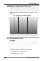
The CG635 has fifty-one, overlapping octave bands. They are summarized in Table 11.
Table 11: CG635's Fifty-one, Overlapping Octave Bands
Band
0
1
2
3
4
5
6
7
8
9
10
11
…
49
50
Divider
1
2
4
8
16
32
64
128
256
512
1024
2048
…
249
250
Min Frequency (Hz)
960,000,000
480,000,000
240,000,000
120,000,000
60,000,000
30,000,000
15,000,000
7,500,000
3,750,000
1,875,000
937,500
468,750
…
0.000,001,705,302
0.000,000,852,651
Max Frequency (Hz)
2,050,000,000
1,024,000,000
512,000,000
256,000,000
128,000,000
64,000,000
32,000,000
16,000,000
8,000,000
4,000,000
2,000,000
1,000,000
…
0.000,003,637,978
0.000,001,818,989
When the user changes the frequency, the CG635 attempts to stay within the same
octave. If an octave switch is required, however, and the frequency is in one of the first
eleven bands, the CG635 will disable the output, forcing it low before changing the
divider and slewing the RF VCO to the new frequency. When the VCO has settled at the
new frequency, the output will be re-enabled in a “runtless” fashion. This is done to
protect the user’s application from spurious clock pulses and frequencies as the dividers
are changed.
For frequencies in bands eleven to fifty, the CG635 uses DDS technology to seamlessly
change dividers. Since no spurious pulses are generated, the output is not disabled.
In addition to the normal methods of stepping frequency by the current step size, the user
can also step the frequency by factors of two by accessing the secondary functions
FREQ/2 and FREQx2.
Phase
The CG635 can adjust the phase of the output by up to 360° per step. The phase may be
set to arbitrary values, or stepped up and down by configurable step sizes by following
the instructions described in the Front-Panel User Interface section at the beginning of
this chapter. If the user enters a phase that requires the output to adjust by more than
360°, the CG635 will briefly display “Step Error” and leave the phase unchanged.
CG635 Synthesized Clock Generator
Operation
21
The CG635 will integrate phase steps in the main display until the phase reaches ±720°,
at which point it will wrap the phase back to 0°. For example, if the current phase is 700°,
and the user steps the phase 90°, the CG635 will display 70°.
The phase resolution of the CG635 is frequency dependent and is summarized in
Table 12.
Table 12: Phase Resolution versus Frequency
Frequency
200 MHz < f ≤ 2.05 GHz
20 MHz < f ≤ 200 MHz
2 MHz < f ≤ 20 MHz
200 kHz < f ≤ 2 MHz
20 kHz < f ≤ 200 kHz
2 kHz < f ≤ 20 kHz
200 Hz < f ≤ 2 kHz
20 Hz < f ≤ 200 Hz
2 Hz < f ≤ 20 Hz
1 µHz ≤ f ≤ 2 Hz
Phase Resolution
1°
0.1°
0.01°
0.001°
0.0001°
0.00001°
0.000001°
0.0000001°
0.00000001°
0.000000001°
If the user tries to enter a phase with more resolution than permitted, the CG635 will
truncate the result to the appropriate resolution.
When the user changes frequency, the CG635 will automatically reset the phase to 0°,
and truncate the phase step size to the resolution allowed at the new frequency. For
example, let the current phase and phase step size be 123.456° and 0.0001°, respectively.
If the user changes the frequency to 100 MHz, the CG635 will change the phase and
phase step sizes to 0.0° and 0.1°.
The user can define the current phase to be zero degrees by accessing the secondary
function REL θ = 0°. The secondary function, θ + 90°, is also available for advancing the
phase by 90°.
For frequencies greater than or equal to 1 Hz, the CG635 adjusts phase by increasing or
decreasing the frequency for a short interval of time to advance or retard the phase by the
desired amount. This is the case even when the phase step is 360°. Advancing phase by
360° results in one extra cycle being inserted over the time period of the phase shift.
Similarly, retarding phase by 360° results in one less cycle being inserted over the time
period of the phase shift.
In most cases, phase shifts take less than 150 ms to complete. At low frequencies,
however, backward phase shifts can take significantly longer. This is simply due to the
fact that the frequency can not be shifted below 0 Hz. Therefore, a backwards phase shift
of 360° at 1 Hz takes a minimum of one second to complete. Arming circuitry in the
CG635 may add an additional 0.5 seconds to that time.
For frequencies less than 1 Hz, the CG635 does “instantaneous” phase shifts using DDS
techniques. In contrast to phase shifts at frequencies above 1 Hz, a 360° phase shift at
CG635 Synthesized Clock Generator
Operation
22
frequencies less than 1 Hz is equivalent to doing nothing. Extra cycles are not inserted or
deleted as part of the phase shift.
The current phase is stored as part of the instrument settings when the user stores and
recalls settings. However, the current phase only has meaning at the current frequency.
Therefore, the phase will only be recalled if the recall of settings does not alter the
current frequency and does not result in a phase shift larger than 360°. Otherwise, the
phase will be simply set to zero.
Secondary Functions
Most of the keys in the ENTRY section of the front panel have secondary functions
associated with them. The names of these functions are printed above the key. The ‘4’
key, for example, has FREQx2 above it.
To access these secondary functions, follow the instructions described in the Front-Panel
User Interface section at the beginning of this chapter. Details about each of the
functions follow.
RUN, STOP, TOGGLE
Normally, the CG635 drives the front-panel outputs with square waves at the selected
frequency, phase, and amplitude settings. The STOP function causes the CG635 to
disable oscillation and force the outputs to a logic low state. When the outputs are in the
stopped state, the STOP LED will blink. Once outputs are stopped, the TOGGLE
function can be used to toggle the state of the outputs. The RUN function restores the
CG635 outputs to normal, running operation.
The run/stop state of the instrument is saved when instrument settings are saved.
INIT
The INIT function causes the CG635 to return to default settings. This function is not
executed until the user presses ‘Hz.’ Table 15 itemizes the CG635 default settings. The
remote interface, GPIB address, and power-on status clear are not affected by this
command, however.
STATUS
The STATUS function displays a number of instrument parameters which characterize
the current status of the CG635. The user can cycle through each of the parameters by
pressing the MODIFY ▲ and ▼ keys. The meaning of each of the parameters is
summarized in Table 13.
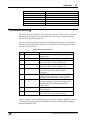
Table 13: Status Parameters
Label
STATUS
SYNTH
ERRORS
Description
CG635 serial poll status byte
Current lock state of CG635
Number of errors in the error buffer
CG635 Synthesized Clock Generator
Operation
R
N
D
FT3
FT2
FT1
FT0
PRBS
RB
23
RF synthesizer R parameter
RF synthesizer N parameter
Divider = 2D
Bits 48-63 of the frequency tuning word
Bits 32-47 of the frequency tuning word
Bits 16-31 of the frequency tuning word
Bits 0-15 of the frequency tuning word
PRBS on/off/disabled status (if installed)
Rb stability (if installed)
The STATUS parameter displays the current value of the CG635 serial poll status byte.
This is the same value that is returned by the *STB? command. See the CG635 Remote
Programming chapter for information on how to interpret the status byte.
The SYNTH parameter displays the current lock status of CG635. The interpretation of
each lock status bit is summarized in Table 14. The red UNLK LED will be on when any
of these bits is set. If the SYNTH parameter is 3, for example, then the RF and 19 MHz
PLLs are currently unlocked.
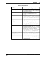
Table 14: Synthesizer Lock Status
Bit
0
1
2
3
4
5
6
7
Name
RF_UNLOCK
19MHZ_UNLOCK
10MHZ_UNLOCK
RB_UNLOCK
OUTPUT_DISABLED
PHASE_SHIFT
Reserved
Reserved
Meaning
RF PLL is unlocked.
19 MHz PLL is unlocked
10 MHz PLL is unlocked
Optional Rb oscillator is unlocked
The output is disabled
The output is scheduled to shift phase.
The interpretation of the SYNTH parameter is similar to that of the lock status register
(LCKR? command). The difference is that the SYNTH parameter bits indicate the current
state of each bit, while the lock status register bits indicate whether the bits have been set
since the register was last read.
The ERRORS parameter displays the number of errors currently stored in the error
buffer. The errors may be retrieved one by one over the remote interface by repeatedly
sending the LERR? command. See the CG635 Remote Programming chapter for
information about the meaning of errors returned by the LERR? command.
The parameters R, N, D define the current state of the RF synthesizer. They satisfy the
equation,
f DDS
2D R
=
f OUT ,
N
CG635 Synthesized Clock Generator
Operation
24
where fDDS is frequency being output by the DDS chip, and fOUT is the current output
frequency.
The parameters FT3, FT2, FT1, and FT0 define the current frequency tuning word for the
DDS chip. They satisfy the equation,
f DDS =
FT 3 × 655363 + FT 2 × 65536 2 + FT 1× 65536 + FT 0
× ( M × 20MHz) ,
2 64
where M is the DDS clock multiplier which is normally set to 5. See the Circuit
Description chapter for more information about the operation of the RF synthesizer and
DDS chip.
PRBS ON/OFF
If the PRBS option is installed, the PRBS ON function enables the PRBS output, and the
PRBS OFF disables it. The CG635 will briefly display ‘PRBS on’ or ‘PRBS off’,
respectively, when the functions are accessed.
If the PRBS option is not installed, the CG635 will briefly display ‘no PRBS.’
The PRBS on/off state is saved when instrument settings are saved. If PRBS is installed,
the current status (on/off/disabled) of the PRBS can viewed via the STATUS function. A
status of ‘disabled’ indicates that the PRBS is requested on but disabled because the
current frequency is too high.
FREQ/2, FREQx2
The functions FREQ/2 and FREQx2 cause the CG635 to decrease or increase the current
frequency by a factor of two. They also force the CG635 to display frequency.
REL θ = 0
This function defines the current phase to be zero degrees. It does not affect the output. It
also forces the CG635 to display phase.
θ + 90°
This function advances the current phase by 90°. It also forces the CG635 to
display phase.
GPIB
This function enables the GPIB remote interface and disables the RS-232 remote
interface. The CG635 will briefly display ‘Enabled’ after enabling the interface. This
function is not executed until the user presses ‘Hz’. The GPIB LED in the INTERFACE
section of the front panel will be on when GPIB is the selected interface.
CG635 Synthesized Clock Generator
Operation
25
ADDRS
This function sets the CG635’s primary GPIB address. The user can enter an address
using the numeric keys or the MODIFY ▲ and ▼ keys. The address is not set until the
user presses the ‘Hz’ key. For example, to set the GPIB address to 23, press the keys
‘SHIFT’, ‘ADDRS’, ‘2’, ‘3’, ‘Hz’ sequentially. The CG635 will briefly display
‘Changed’ if the address changes.
The factory default GPIB address is 23.
RS-232
This function enables the RS-232 remote interface and disables the GPIB remote
interface. The CG635 will briefly display ‘Enabled’ after enabling the interface. This
function is not executed until the user presses ‘Hz’. The RS-232 LED in the
INTERFACE section of the front panel will be on when RS-232 is the selected interface.
The communication parameters are fixed at: 9600 Baud rate, 8 Data bits, 1 Stop bit, No
Parity, RTS/CTS Hardware Flow Control.
DATA
This function enables the user to see the most recent characters received by the CG635
over the remote interface. The characters are shown in hexadecimal format, with older
characters appearing to the left and newer characters appearing to the right. The last
character received is marked with the decimal point showing.
To move back and forth through the buffer, use the MODIFY ▲ and ▼ keys.
Factory Default Settings
The factory default settings are listed in Table 15. The CG635 may be forced to assume
its factor default settings by power cycling the unit with the ‘BACK SPACE’ key
depressed. The INIT secondary function and the *RST remote command reset all but the
communication parameters back to factory default settings.
Table 15: Factory Default Settings
Parameter
Frequency
Frequency step size
Phase
Phase step size
Q / Q̄ high
Q / Q̄ high step size
Q / Q̄ low
Q / Q̄ low step size
CMOS high
CMOS high step size
CMOS low
CMOS low step size
Setting
10 MHz
1 Hz
0°
1°
1.43 V (LVDS)
0.1 V
1.07 V (LVDS)
0.1 V
3.3 V (+3.3 V CMOS)
0.1 V
0.0 V (+3.3 V CMOS)
0.1 V
CG635 Synthesized Clock Generator
Operation
PRBS
Run/stop state
Display
Display on/off state
Enabled remote interface
GPIB address
Power-on Status Clear (*PSC)
26
Off
Running
Frequency
On
RS-232
23
1
Troubleshooting
The CG635 does not include any user serviceable parts inside. The line fuse is internal to
the instrument and may not be serviced by the user. In the event of instrument failure,
refer service to a qualified technician.
The CG635 performs several instrument tests during startup. The tests are described in
Table 16. In most cases the unit will have to be repaired by a qualified technician if the
unit fails one of these tests.
Table 16: Power-On Self Tests
Test Description
ROM ROM checksum
1
2
24V Power
19.44 MHz tuning
3
19.40 MHz tuning
4
RF VCO
5
CMOS output
6
Q / Q̄ outputs
7
Clock symmetry
8
Option detection
Test Fail Symptoms
Flash memory is corrupted. Unit may behave
unpredictably
Power supply is not providing stable 24 volts.
The crystal can’t tune to ±100 ppm. The CG635
may not be able to lock at all frequencies.
The crystal can’t tune to ±100 ppm. The CG635
may not be able to lock at all frequencies.
The VCO can’t tune from 960MHz to 2.05 GHz.
The CG635 may not be able to lock at all
frequencies.
The CG635 is unable to drive the front-panel
CMOS output to the correct voltage. Check that
the output is not connected to a voltage source.
The CG635 is unable to drive the Q / Q̄ outputs to
the correct voltages. Check that the outputs are
terminated into 50 Ω and not connected to a
voltage source.
Output duty cycle is not 50 %. Output driver is
likely damaged.
Optional oscillator is installed, but not oscillating.
The CG635 will use its internal oscillator.
Table 17 contains a list of troubleshooting tips for various symptoms which may occur in
a normally functioning unit. Please consult this list before contacting SRS regarding a
potential instrument failure.
CG635 Synthesized Clock Generator
Operation
27
Table 17: Troubleshooting Tips
Symptom
STOP LED flashing and output
not oscillating
CMOS output not oscillating
RS-485 output not oscillating
PRBS outputs not functioning
UNLK LED flashes once a
second
No GPIB communication
No RS-232 communication
Doesn’t respond to key presses
and REM LED is on
ERR LED flashes
Resolution
Output is in stopped state. To put back into running
state, sequentially press ‘SHIFT’, ‘RUN’
The front-panel CMOS output is forced to a low
state at frequencies above 250 MHz. Try setting the
frequency below 250 MHz.
The rear panel RS-485 output is disabled above
105 MHz. Try setting the frequency below
105 MHz.
Make sure PRBS is enabled. Press ‘SHIFT’,
‘PRBS ON’ to enable. The PRBS is also disabled
above 1.55 GHz. Try setting the frequency below
1.55 GHz.
An optional rubidium oscillator is installed but it is
not yet stable. Wait 10 minutes to give the
rubidium time to warm up and stabilize.
Check that GPIB communication is enabled.
Sequentially press ‘SHIFT’, ‘GPIB’, ‘Hz’. Also
check that the GPIB address is set correctly. See
the ADDRS secondary function.
Check that RS-232 communication is enabled.
Sequentially press ‘SHIFT’, ‘RS-232’, ‘Hz’. Also
check that the communication parameters are set to
9600 baud, 8 bits, no parity, one stop bit and
RTS/CTS hardware flow control. When connecting
to a PC, make sure you are using a standard PC
serial cable, not a “null-modem” cable.
The CG635 has been placed in remote mode by the
GPIB bus. Press ‘STEP SIZE’ to put the CG635
back into local mode.
The CG635 has received characters over the
remote interface, but the command parser has
determined that the command is invalid. Check the
command syntax and make sure you are appending
a command terminator.
CG635 Synthesized Clock Generator
CG635 Remote Programming
29
CG635 Remote Programming
Introduction
The CG635 may be remotely programmed via the standard GPIB interface or the RS-232
serial interface. Any host computer interfaced to the CG635 can easily control and
monitor the operation of the CG635.
GPIB
The CG635 comes with an IEEE 488 standard port for communicating over GPIB. The
port is located on the rear panel of the CG635.
This interface is enabled via the front panel by pressing the keys ‘SHIFT’, ‘GPIB’, ‘Hz’.
The primary GPIB address of the instrument is also set via the front panel by pressing the
keys ‘SHIFT’, ‘ADDRS’, MODIFY ▲ or ▼, ‘Hz’. Valid GPIB addresses range from 0
to 30. Enabling the GPIB interface causes the RS-232 interface to be disabled. The GPIB
LED in the INTERFACE section of the front panel will be on when GPIB is the
selected interface.
The factory default GPIB address is 23.
RS-232
The CG635 comes standard with an RS-232 communications port. The port is located on
the rear panel of the CG635.
The RS-232 interface connector is a standard 9 pin, type D, female connector configured
as a DCE (transmit on pin 3, receive on pin 2). The communication parameters are fixed
at: 9600 Baud rate, 8 Data bits, 1 Stop bit, No Parity, RTS/CTS Hardware Flow Control.
This interface is enabled via the front panel by pressing the keys ‘SHIFT’, ‘RS-232’,
‘Hz’. Enabling the RS-232 interface causes the GPIB interface to be disabled. The
RS-232 LED in the INTERFACE section of the front panel will be on when RS-232 is
the selected interface.
Front-Panel Indicators
To assist in programming, the CG635 has four front panel indicators located under the
INTERFACE section: RS-232, GPIB, ACT, and ERR. The RS-232 LED is on when the
CG635 is configured to accept commands over RS-232. The GPIB LED is on when the
CG635 is configured to accept commands over GPIB. The ACT LED serves as an
activity indicator that flashes every time a character is received or transmitted over one of
the remote interfaces. The ERR LED will flash when a remote command fails to execute
due to illegal syntax or invalid parameters.
CG635 Synthesized Clock Generator
CG635 Remote Programming
30
Command Syntax
Communications with the CG635 is done with ASCII characters. All commands are
4-characters long and are case-insensitive. Standard IEEE-488.2 defined commands
begin with the ‘*’ character followed by three letters. CG635 specific commands are
composed of four letters.
The four-letter mnemonic (shown in CAPS) in each command sequence specifies the
command. The rest of the sequence consists of parameters.
Commands may take either set or query form, depending on whether the ‘?’ character
follows the mnemonic. Set only commands are listed without the ‘?’, query only
commands show the ‘?’ after the mnemonic, and optionally query commands are marked
with a ‘(?)’.
Parameters shown in { } and [ ] are not always required. Parameters in { } are required to
set a value, and are omitted for queries. Parameters in [ ] are optional in both set and
query commands. Parameters listed without any surrounding characters are
always required.
Do NOT send () or {} or [] or spaces as part of the command.
The command buffer is limited to 255 bytes, with 25 byte buffers allocated to each of up
to three parameters per command. If the command buffer overflows, both the input and
output buffers will be flushed and reset. If a parameter buffer overflows, a command
error will be generated and the offending command discarded.
Commands are terminated by either a semicolon, a <CR> (ASCII 13), or a <LF> (ASCII
10). If the communications interface is GPIB, then the terminating character may
optionally be accompanied by an EOI signal. If the EOI accompanies a character other
than a <LF>, a <LF> will be appended to the command to terminate it. Execution of the
command does not begin until a command terminator is received.
Aside from communication errors, commands may fail due to either syntax or execution
errors. Syntax errors can be detected by looking at bit 5 (CME) of the event status
register (*ESR?). Execution errors can be detected by looking at bit 4 (EXE) of the event
status register. In both cases, an error code, indicating the specific cause of the error, is
appended to the error queue. The error queue may be queried with the LERR? command.
Descriptions of all error codes can be found in the Error Codes section starting on
page 43.
CG635 Synthesized Clock Generator
CG635 Remote Programming
31
Index of Commands
Instrument Control Commands
CMOS(?) i,{j}
DISP(?){i}
FREQ(?){i}
PHAS(?){i}
PRBS(?){i}
QOUT(?) i,{j}
RPHS
RUNS(?){i}
SHDP(?){i}
SLVL(?){i}
STDC(?){i}
STDQ(?){i}
STPD i
STPS(?) i,{j}
STPU i
TIMB?
UNIT(?) i,{j}
Page 32
Page 32
Page 32
Page 32
Page 32
Page 32
Page 33
Page 33
Page 33
Page 33
Page 33
Page 33
Page 34
Page 34
Page 34
Page 34
Page 34
CMOS Output
Display
Frequency
Phase
Enable PRBS
Q / Q̄ Output
Relative Phase
Running State
Show Display
Stop Level
Standard CMOS
Standard Q / Q̄
Step Down
Step Size
Step Up
Timebase
Units Display
Interface Commands
*IDN?
*OPC(?)
*RCL i
*RST
*SAV i
*TST?
*WAI
Page 36
Page 36
Page 36
Page 36
Page 36
Page 37
Page 37
Identification String
Operation Complete
Recall Instrument Settings
Reset the Instrument
Save Instrument Settings
Self Test
Wait for Command Execution
Status Reporting Commands
*CLS
*ESE(?){i}
*ESR?
*PSC(?){i}
*SRE(?){i}
*STB?
CESE(?){i}
CESR?
INSE(?){i}
INSR?
LCKE(?){i}
LCKR?
LERR?
Page 38
Page 38
Page 38
Page 38
Page 38
Page 38
Page 39
Page 39
Page 39
Page 39
Page 39
Page 39
Page 39
Clear Status
Standard Event Status Enable
Standard Event Status Register
Power-on Status Clear
Service Request Enable
Serial Poll Status Byte
Communication Error Status Enable
Communication Error Status Register
Instrument Status Enable
Instrument Status Register
PLL Lock Status Enable
PLL Lock Status Register
Last Error
CG635 Synthesized Clock Generator
CG635 Remote Programming
32
Instrument Control Commands
CMOS(?) i,{j}
CMOS Output
Set (query) the ith component of the CMOS output {to j}.
The parameter i selects the CMOS component.
i
Value
0
CMOS low voltage
1
CMOS high voltage
Example
CMOS 1, 2.5<CR> Set CMOS high to 2.5 volts.
CMOS?0<CR>
Query CMOS low voltage.
DISP(?){i}
Display
Set (query) the current display value {to i}.
The parameter i selects the display type.
i
Display
0
Frequency
1
Phase
2
Q / Q̄ high
3
Q / Q̄ low
4
CMOS high
5
CMOS low
6
Frequency step
7
Phase step
8
Q / Q̄ high step
9
Q / Q̄ low step
10
CMOS high step
11
CMOS low step
The query form returns –1 if the current display does not correspond to one of the
standard displays. This might occur, for example, if one of the status displays
were active.
FREQ(?){i}
Frequency
Set (query) the frequency {to i}.
PHAS(?){i}
Phase
Set (query) the phase {to i}. Note that this command is executed as an
overlapped operation. If necessary, use *OPC or *WAI to determine when the
operation is complete.
PRBS(?){i}
Enable PRBS
Set (query) the PRBS enabled state {to i}. If i is 0, PRBS is disabled. If i is 1,
PRBS is enabled.
QOUT(?) i,{j}
Q / Q̄ Output
Set (query) the ith component of the Q / Q̄ output {to j}.
The parameter i selects the Q / Q̄ component.
CG635 Synthesized Clock Generator
CG635 Remote Programming
i
0
1
33
Value
Q / Q̄ low voltage
Q / Q̄ high voltage
Example
QOUT 1, 2.1<CR> Set Q / Q̄ high voltage to 2.1 volts.
QOUT?0<CR>
Query Q / Q̄ low voltage.
RPHS
Relative Phase
Define the current phase to be zero degrees. This command does not affect
the output.
RUNS(?){i}
Running State
Set (query) the running state of outputs {to i}. If i is 0, the outputs are in the
stopped state. RUNS 0 stops the output and also sets stop level low. If i is 1, the
output is not stopped.
SHDP(?){i}
Show Display
Set (query) the current state of the display. If i is 0, the display is turned off. If i
is 1, the display is turned on.
SLVL(?){i}
Stop Level
Set (query) the level at the output in the stopped state {to i}. If i is 0, the stop
level is low. If i is 1, the stop level is high. If i is set to 2, the stop level
is toggled.
STDC(?){i}
Standard CMOS
Set (query) the CMOS output {to i}.
The parameter i selects the standard level.
i
Standard CMOS Level
0
1.2 V standard CMOS
1
1.8 V standard CMOS
2
2.5 V standard CMOS
3
3.3 V standard CMOS
4
5.0 V standard CMOS
The query form returns –1 if the current levels do not correspond to one of the
standard levels. This indicates that the VAR LED is on.
STDQ(?){i}
Standard Q / Q̄
Set (query) the Q / Q̄ outputs {to i}.
The parameter i selects the standard level.
i
Standard Q / Q̄ Level
0
ECL levels (–1.00/–1.80 V)
1
+7 dBm levels (+0.50/–0.50 V)
2
LVDS levels (1.43/1.07 V)
3
PECL 3.3 V levels (2.30/1.50 V)
4
PECL 5.0 V levels (4.00/3.20 V)
The query form returns 1 if the current levels do not correspond to one of the
standard levels. This indicates that the VAR LED is on.
CG635 Synthesized Clock Generator
CG635 Remote Programming
STPD i
Step Down
Step down the ith component.
The parameter i selects the component to step.
i
Value
0
Step the frequency
1
Step the phase
2
Step Q / Q̄ high
3
Step Q / Q̄ low
4
Step CMOS high
5
Step CMOS low
STPS(?) i,{j}
Step Size
Set (query) the ith step size {to j}.
The parameter i selects the component.
i
Value
0
Frequency step size in Hz
1
Phase step size in degrees
2
Q / Q̄ high step size in volts
3
Q / Q̄ low step size in volts
4
CMOS high step size in volts
5
CMOS low step size in volts
34
Example
STPS 1,2.0<CR> Set the phase step size to 1 degree.
STPS?0<CR>
Query the frequency step size.
STPU i
Step Up
Step up the ith component.
The parameter i selects the component to step.
i
Value
0
Step the frequency
1
Step the phase
2
Step Q / Q̄ high
3
Step Q / Q̄ low
4
Step CMOS high
5
Step CMOS low
TIMB?
Timebase
Query the current timebase for the CG635.
The returned value identifies the timebase.
Value Meaning
0
Internal timebase
1
OCXO timebase
2
Rubidium timebase
3
External timebase
UNIT(?) i,{j}
Units Display
Set (query) the units for display value {to j}.
CG635 Synthesized Clock Generator
CG635 Remote Programming
35
The parameter i selects the item.
i
Display Item
0
Frequency
1
Frequency Step
The parameter j selects the units.
Display
j
0
Hz
1
kHz
2
MHz
3
GHz
CG635 Synthesized Clock Generator
CG635 Remote Programming
36
Interface Commands
*IDN?
Identification String
Query the instrument identification string.
Example
*IDN?<CR>
Returns a string similar to ‘Stanford Research
Systems,CG635,s/n004025,ver0.01’
*OPC(?)
Operation Complete
The set form sets the OPC flag in the ESR register when all prior commands
have completed. The query form returns ‘1’ when all prior commands have
completed, but does not affect the ESR register.
*RCL i
Recall Instrument Settings
Recall instrument settings from location i. The parameter i may range from
0 to 10. Locations 0 to 9 are for arbitrary use. Location 10 is reserved for the
instrument’s current settings. This location is automatically updated 60 seconds
after the user presses any key that modifies the current state of the instrument.
The following settings are recalled:
1. Current frequency and frequency step size.
2. Current phase and phase step size.
3. Q / Q̄ high and low levels and step sizes.
4. CMOS high and low levels and step sizes.
5. Current display selection.
6. PRBS on/off state
7. Run/stop state
8. Stop level
The display will be turned on when settings are recalled.
Example
*RCL 3<CR>
*RST
Recall instruments settings from location 3.
Reset the Instrument
Reset the instrument to default settings. This is equivalent to pressing the keys
‘SHIFT’, ‘INIT’, ‘Hz’ on the front panel. The factory default settings are listed in
Table 15. . The remote interface, GPIB address, and power-on status clear are not
affected by this command, however.
Example
*RST<CR>
*SAV i
Resets the instrument to default settings
Save Instrument Settings
Save instrument settings to location i. The parameter i may range from 0 to 10.
Locations 0 to 9 are for arbitrary use. Location 10 is reserved for the instrument’s
current settings. This location is automatically updated ten seconds after the user
presses any key that modifies the current state of the instrument. The following
settings are saved:
1. Current frequency and frequency step size.
2. Current phase and phase step size.
CG635 Synthesized Clock Generator
CG635 Remote Programming
37
3. Q / Q̄ high and low levels and step sizes.
4. CMOS high and low levels and step sizes.
5. Current display selection.
6. PRBS on/off state
7. Run/stop state
8. Stop level
Example
*SAV 3<CR>
*TST?
Save current settings to location 3.
Self Test
Runs the instrument self test and returns 0 if successful and 72
(EXE_FAIL_SELF_TEST) if unsuccessful. If unsuccessful, the error buffer will
include device dependent errors related to the parts of the self test that failed.
Example
*TST?<CR>
*WAI
Run the instrument self test and return the result.
Wait for Command Execution
The instrument will not process further commands until all prior commands
including this one have completed.
Example
*WAI<CR>
Wait for all prior commands to execute before continuing.
CG635 Synthesized Clock Generator
CG635 Remote Programming
38
Status Reporting Commands
*CLS
Clear Status
Clear Status immediately clears the ESR, CESR, LCKR, and INSR registers as
well as the LERR error buffer.
*ESE(?){i}
Standard Event Status Enable
Set (query) the standard event status enable register {to i}. Bits set in this register
cause ESB in the serial poll status byte to be set when the corresponding bit is set
in the standard event status register.
*ESR?
Standard Event Status Register
Query the standard event status register. The value returned is a decimal value
from 0 to 255. After executing a *ESR? query, the register is cleared. See the
Status Byte Definitions section for a description of each of the bits.
Example
*ESR?<CR>
*PSC(?){i}
A return of ‘176’ would indicate that PON, CME, and EXE
are set.
Power-on Status Clear
Set (query) the Power-on Status Clear flag {to i}. The Power-on Status Clear flag
is stored in nonvolatile memory in the CG635, and thus, maintains its value
through power-cycle events.
If the value of the flag is 0, then the Service Request Enable and Standard Event
Status Enable Registers (*SRE, *ESE) are stored in non-volatile memory, and
retain their values through power-cycle events. If the value of the flag is 1, then
these two registers are cleared upon power-cycle.
Example
*PSC 1<CR>
*PSC?<CR>
Set the Power-on Status Clear to 1.
Returns the current value of Power-on Status Clear.
*SRE(?){i}
Service Request Enable
Set (query) the Service Request Enable register {to i}. Bits set in this register
cause the CG635 to generate a service request when the corresponding bit is set
in the serial poll status register.
*STB?
Serial Poll Status Byte
Query the standard IEEE 488.2 serial poll status byte. The value returned is a
decimal value from 0 to 255. Reading this byte has no effect on its value. See the
Status Byte Definitions section for a description of each of the bits.
Example
*STB?<CR>
A return of ‘114’ would indicate that LCKB, MAV, ESB, and
MSS are set. LCKB indicates that an enabled bit in LCKR is
set. MAV indicates that a message is available in the output
queue. ESB indicates that an enabled bit in ESR is set. MSS
reflects the fact that at least one of the summary bits is set.
CG635 Synthesized Clock Generator
CG635 Remote Programming
39
CESE(?){i}
Communication Error Status Enable
Set (query) the communications error status enable register {to i}. Bits set in this
register cause CESB in the serial poll status byte to be set when the
corresponding bit is set in the communications error status register (CESR).
CESR?
Communication Error Status Register
Query the communications error status register. The value returned is a decimal
value from 0 to 255. After executing a CESR? query, the register is cleared. See
the Status Byte Definitions section for a description of each of the bits.
Example
CESR?<CR>
A return of ‘24’ would indicate that OR and OVFL bits are
set. OR indicates that a character was received over RS-232
before the microcontroller had time to process the previous
character. OVFL indicates that the input buffer overflowed.
INSE(?){i}
Instrument Status Enable
Set (query) the instrument status enable register {to i}. Bits set in this register
cause INSB in the serial poll status byte to be set when the corresponding bit is
set in the instrument status register (INSR).
INSR?
Instrument Status Register
Query the instrument status register. The value returned is a decimal value from
0 to 255. After executing a INSR? query, the register is cleared. See the Status
Byte Definitions section for a description of each of the bits.
Example
INSR?<CR>
A return of ‘4’ would indicate that an eeprom write failed.
LCKE(?){i}
PLL Lock Status Enable
Set (query) the PLL lock status enable register {to i}. Bits set in this register
cause LCKB in the serial poll status byte to be set when the corresponding bit is
set in the PLL lock status register (LKCR).
LCKR?
PLL Lock Status Register
Query the PLL lock status register. The value returned is a decimal value from
0 to 255. After executing a LCKR? query, the register is cleared. See the Status
Byte Definitions section for a description of each of the bits.
Example
LCKR?<CR>
LERR?
A return of ‘3’ would indicate that the RF PLL and the
19 MHz PLL have come unlocked.
Last Error
Query the last error in the error buffer. After executing a LERR? query, the
returned error is removed from the error buffer. See the Error Codes section later
in this chapter for a description of the possible error codes returned by LERR?.
The error buffer has space to store up to 20 errors. If more than 19 errors occur
without being queried, the 20th error will be 254 (Too Many Errors) indicating
that errors were dropped.
CG635 Synthesized Clock Generator
CG635 Remote Programming
40
Status Byte Definitions
The CG635 reports on its status by means of the serial poll status byte and four event
status registers: the standard event status (*ESR), the communication error status
(CESR), the PLL lock status (LCKR), and the instrument event status (INSR). These
read-only registers record the occurrence of defined events inside the CG635. If the event
occurs, the corresponding bit is set to one. Bits in the status registers are latched. Once an
event bit is set, subsequent state changes do not clear the bit. Bits are cleared when the
registers are queried, with a *ESR?, for example. The bits are also cleared with the clear
status command, *CLS. The bits are not cleared, however, with an instrument reset
(*RST) or a device clear.
Each of the CG635’s four event status registers has an associated enable register. The
enable registers control the reporting of events in the serial poll status byte (*STB). If a
bit in the event status register is set and its corresponding bit in the enable register is set,
then the summary bit in the serial poll status byte (*STB) will be set. The enable registers
are readable and writable. Reading the enable registers or clearing the status registers
does not clear the enable registers. Bits in the enable registers must be set or cleared
explicitly. To set bits in the enable registers, write an integer value equal to the binary
weighted sum of the bits you wish to set.
The serial poll status byte (*STB) also has an associated enable register called the service
request enable register (*SRE). This register functions in a similar manner to the other
enable registers, except that it controls the setting of the master summary bit (bit 6) of the
serial poll status byte. It also controls whether the CG635 will issue a request for service
on the GPIB bus.
Serial Poll Status Byte
Bit
0
Name
INSB
1
LCKB
2
CESB
3
4
5
Reserved
MAV
ESB
6
MSS
7
Reserved
Meaning
An unmasked bit in the instrument status register (INSR) has
been set.
An unmasked bit in the PLL lock status register (LCKR) has
been set.
An unmasked bit in the communications status register (CESR)
has been set.
The interface output buffer is non-empty.
An unmasked bit in the standard event status register (*ESR)
has been set.
Master summary bit. Indicates that the CG635 is requesting
service because an unmasked bit in this register has been set.
The serial poll status byte may be queried with the *STB? command. The service request
enable register (*SRE) may be used to control when the CG635 asserts the request-forservice line on the GPIB bus.
CG635 Synthesized Clock Generator
CG635 Remote Programming
41
Standard Event Status Register
Bit
0
Name
OPC
1
2
3
4
Reserved
QYE
DDE
EXE
5
6
7
CME
Reserved
PON
Meaning
Operation complete. All previous commands have completed.
See command *OPC.
Query error occurred.
Device dependent error.
Execution error. A command failed to execute correctly
because a parameter was out of range.
Command error. The parser detected a syntax error
Power on. The CG635 has been power cycled.
The standard event status register may be queried with the *ESR? command. The
standard event status enable register (*ESE) may be used to control the setting of the
ESB summary bit in the serial poll status byte.
Communication Error Status Register
Bit
0
1
2
Name
PE
FE
NF
3
OR
4
5
OVFL
NL
6
7
Reserved
DCAS
Meaning
Parity error. An RS-232 parity error was detected.
Framing error. An RS-232 framing error was detected.
Noise flag. An RS-232 character may have been received
incorrectly due to noise on the line.
Overrun error. An RS-232 character was received before the
CG635 had time to process the previous character.
The input buffer of the CG635 overflowed.
The CG635 was addressed to talk under GPIB, but there were
no listeners.
Device clear active state. The CG635 received a device clear or
selected device clear command.
The communication error status register may be queried with the CESR? command. The
communication error status enable register (CESE) may be used to control the setting of
the CESB summary bit in the serial poll status byte.
Instrument Status Register
Bit
0
1
2
3
4
5
6
7
Name
Meaning
EE_BDRY
Eeprom write occurred outside of eeprom.
EE_PROT
Eeprom write occurred in protected eeprom.
EE_VERF
Eeprom write failed to verify.
CMF_RESET A clock-monitor-fail reset has occurred.
COP_RESET A COP-timeout reset has occurred.
ILGL_RESET An illegal-instruction reset has occurred.
RB_COMM
An installed rubidium oscillator failed to communicate.
Reserved
CG635 Synthesized Clock Generator
CG635 Remote Programming
42
The instrument status register may be queried with the INSR? command. The instrument
status enable register (INSE) may be used to control the setting of the INSB summary bit
in the serial poll status byte.
PLL Lock Status Register
Bit
0
1
2
3
4
5
6
7
Name
Meaning
RF_UNLOCK
The RF PLL has come unlocked.
19MHZ_UNLOCK The 19 MHz PLL has come unlocked.
10MHZ_UNLOCK The 10 MHz PLL has come unlocked.
RB_UNLOCK
The optional rubidium oscillator has come unlocked.
OUT_DISABLED The output was disabled.
PHASE_SHIFT
The output has or is scheduled to shift phase.
Reserved
Reserved
The PLL lock status register may be queried with the LCKR? command. The PLL status
enable register (LCKE) may be used to control the setting of the LCKB summary bit in
the serial poll status byte.
CG635 Synthesized Clock Generator
CG635 Remote Programming
43
Error Codes
The CG635 contains an error buffer that may store up to 20 error codes associated with errors
encountered during power-on self tests, command parsing, or command execution. The errors in the
buffer may be read one by one by executing successive LERR? commands. The meaning of each of the
error codes is described below.
Execution Errors
0
No Error
No more errors left in the queue.
10
Illegal Value
A parameter was out of range.
20
Frequency Error
The frequency or frequency step size was illegal.
30
Phase Error
The phase step size was illegal.
31
Phase Step Error
The phase could not be set because it would have caused a phase step larger than 360°.
40
Voltage Error
The voltage could not be set because it was out of range.
51
Q / Q̄ Low Changed
Q / Q̄ high was set to the requested value, but Q / Q̄ low was also changed in order to
satisfy the Q / Q̄ amplitude limits.
52
Q / Q̄ High Changed
Q / Q̄ low was set to the requested value, but Q / Q̄ high was also changed in order to
satisfy the Q / Q̄ amplitude limits.
61
CMOS Low Changed
CMOS high was set to the requested value, but CMOS low was also changed in order to
satisfy the CMOS amplitude limits.
62
CMOS High Changed
CMOS low was set to the requested value, but CMOS high was also changed in order to
satisfy the CMOS amplitude limits.
71
No PRBS
PRBS could not be enabled because it’s not installed.
CG635 Synthesized Clock Generator
CG635 Remote Programming
72
44
Failed Self Test
The self test failed. The device dependent errors that caused the self test to fail will
follow in the error buffer.
Query Errors
100
Lost Data
Data in the output buffer was lost. This occurs if the output buffer overflows, or if a
communications error occurs and data in output buffer is discarded.
102
No Listener
This is a communications error that occurs if the CG635 is addressed to talk on the GPIB
bus, but there are no listeners. The CG635 discards any pending output.
Parsing Errors
110
Illegal Command
The command syntax used was illegal. A command is normally a sequence of four letters,
or a ‘*’ followed by three letters.
111
Undefined Command
The specified command does not exist.
112
Illegal Query
The specified command does not permit queries
113
Illegal Set
The specified command can only be queried.
114
Null Parameter
The parser detected an empty parameter.
115
Extra Parameters
The parser detected more parameters than allowed by the command.
116
Missing Parameters
The parser detected missing parameters required by the command.
117
Parameter Overflow
The buffer for storing parameter values overflowed. This probably indicates a syntax
error.
118
Invalid Floating Point Number
The parser expected a floating point number, but was unable to parse it.
CG635 Synthesized Clock Generator
CG635 Remote Programming
120
45
Invalid Integer
The parser expected an integer, but was unable to parse it.
122
Invalid Hexadecimal
The parser expected hexadecimal characters, but was unable to parse them.
126
Syntax Error
The parser detected a syntax error in the command.
Device Dependent Errors
151
Failed ROM Check
The ROM checksum failed. The firmware code is likely corrupted.
152
Failed 24 V Out of Range
The CG635 24 V power is out of range.
153
Failed 19.44 MHz Low Rail
The 19.44 MHz crystal can not tune to low enough frequencies.
154
Failed 19.44 MHz High Rail
The 19.44 MHz crystal can not tune to high enough frequencies.
155
Failed 19.40 MHz Low Rail
The 19.40 MHz crystal can not tune to low enough frequencies.
156
Failed 19.40 MHz High Rail
The 19.40 MHz crystal can not tune to high enough frequencies.
157
Failed RF at 2 GHz
The RF VCO could not tune to 2 GHz.
158
Failed RF at 1 GHz
The RF VCO could not tune to 1 GHz.
159
Failed CMOS Low Spec.
The CMOS low output is out of specification.
160
Failed CMOS High Spec.
The CMOS high output is out of specification.
161
Failed Q / Q̄ Low Spec.
The Q / Q̄ low output is out of specification.
CG635 Synthesized Clock Generator
CG635 Remote Programming
162
46
Failed Q / Q̄ High Spec.
The Q / Q̄ high output is out of specification.
163
Failed Optional Timebase
An installed optional timebase is not oscillating.
164
Failed Clock Symmetry
The clock output symmetry is out of specification
Other Errors
254
Too Many Errors
The error buffer is full. Subsequent errors have been dropped.
CG635 Synthesized Clock Generator
Performance Evaluation
47
Performance Evaluation
Overview
The performance of a CG635 may be evaluated by running a series of tests designed to
measure the accuracy of its inputs and outputs and comparing the results with their
associated specifications. While the performance tests presented here are not as extensive
as the tests performed at the factory, one can nevertheless have confidence that a unit that
passes these tests is functioning properly and within specification.
The performance tests can be divided into three broad categories: output driver tests,
frequency synthesis tests, and timebase calibration tests. The output driver tests are
designed to test the integrity and accuracy of the front panel outputs by measuring the
accuracy with which its levels are generated and the speed with which it transitions
between levels. The frequency synthesis tests are designed to measure the stability of the
frequency synthesis by measuring the phase noise and jitter at specified frequencies.
Overall functionality is verified by measuring the frequency generation at various points
in the spectrum from DC to 2.05 GHz. Lastly, the timebase calibration tests evaluate the
accuracy and stability of the installed timebase.
Equipment Required
In addition to the CG635 under test, the following equipment will be required to carry out
the performance tests:
•
•
•
•
•
•
Agilent 34401A digital multimeter
HP 54120A digitizing oscilloscope with HP 54121A four channel input module
CG646 +7 dBm RF receiver module
FS725 rubidium frequency standard
HP 89440A spectrum analyzer
SR620/SR625 time interval counter (SR625 needed to test to 2 GHz)
Equivalent equipment may be substituted as desired as long as they have similar or
superior specifications. Standard SMA and BNC cables will be required to connect the
test equipment to the CG635. Additionally accessories required include, 50 Ω terminators
for the CG635’s high frequency outputs and 20 dB DC to 18 GHz SMA attenuators for
the HP 54121A inputs.
CG635 Self Test
The CG635 includes a self test that checks the functional operation of several internal
components. If any of the tests fail, the CG635 will briefly display “Failed” after the test.
The tests are described in Table 16. In most cases the unit will have to be repaired by a
qualified technician if the unit fails one of these tests.
CG635 Synthesized Clock Generator
Performance Evaluation
48
Table 18: Power-On Self Tests
Test
ROM
Description
ROM checksum
1
2
24V Power
19.44 MHz tuning
3
19.40 MHz tuning
4
RF VCO
5
CMOS output
6
Q / Q̄ outputs
7
Clock symmetry
8
Option detection
Test Fail Symptoms
Flash memory is corrupted. Unit may behave
unpredictably
Power supply is not providing stable 24 volts.
The crystal can’t tune to ±100 ppm. The CG635 may
not be able to lock at all frequencies.
The crystal can’t tune to ±100 ppm. The CG635 may
not be able to lock at all frequencies.
The VCO can’t tune from 960MHz to 2.05 GHz. The
CG635 may not be able to lock at all frequencies.
The CG635 is unable to drive the front-panel CMOS
output to the correct voltage. Check that the output is
not connected to a voltage source.
The CG635 is unable to drive the Q/Q̄ outputs to the
correct voltages. Check that the outputs are terminated
into 50 Ω and not connected to a voltage source.
Output duty cycle is not 50 %. Output driver may be
damaged.
Optional oscillator is installed, but not oscillating. The
CG635 will use its internal oscillator.
The CG635 self test is automatically executed at power-on. It may also be executed by
sending the command *TST? over the remote interface. If the unit passes it will return 0
over the remote interface. If it fails, it will return 72. Refer to the user guide for more
information about communicating with the CG635 over a remote interface.
Output Level Tests
The output level tests are intended to test the accuracy and integrity of the CG635 output
drivers. They test the accuracy of the DC voltage levels at each of the supported
communication standards. They also test the speed with which transitions between levels
occurs.
Q/Q̄ Level Tests
The Q/Q̄ ouput level tests require the setup shown in Figure 4.
Agilent 34401A
50 Ω termination
6½ Digit DVM
50 Ω termination
Q
Q
CMOS
CG635
Figure 4: Q/Q̄ output level test setup
The Q/Q̄ outputs should be terminated into 50 Ω. The terminator connected to the Agilent
DVM should be accurate to 1%. To test the Q output, configure the CG635 as follows:
1. Press ‘SHIFT’, ‘INIT’, ‘Hz’ to return the CG635 to default settings.
CG635 Synthesized Clock Generator
Performance Evaluation
2.
3.
4.
5.
6.
49
Press the Q/Q̄ ▲ and ▼ buttons to select the communication standard under test.
Press ‘SHIFT’, ‘STOP’ to stop the clock outputs at a low level.
Record Vlow as reported by the DVM.
Press ‘SHIFT’, ‘TOGGLE’, ‘SHIFT’ to toggle the clock outputs to a high level.
Record Vhigh as reported by the DVM.
The recorded values (Vlow, Vhigh) should fall between the minimum and maximum values
listed in Table 19 for each standard level.
Table 19: Minimum and Maximum allowed values for the Q/Q̄ outputs
Output
ECL
+7 dBm
LVDS
PECL 3.3V
PECL 5V
Min. (Low, High) V
(–1.828, –1.020)
(–0.515, 0.485)
(1.049, 1.406)
(1.475, 2.267)
(3.158, 3.950)
Measured (Low, High) V
Max. ( Low, High) V
(–1.772, –0.980)
(–0.485, 0.515)
(1.091, 1.454)
(1.525, 2.333)
(3.242, 4.050)
To test the Q̄ output, configure the CG635 as in Figure 4, except swap the connections to
Q and Q̄. Repeat the steps above except record Vhigh in step 4 and record Vlow in step 6.
CMOS Level Tests
The CMOS output level tests require the setup shown in Figure 5.
Agilent 34401A
6½ Digit DVM
Q
Q
CMOS
CG635
Figure 5: CMOS output level test setup
To test the CMOS output, configure the CG635 as follows:
1. Press ‘SHIFT’, ‘INIT’, ‘Hz’ to return the CG635 to default settings.
2. Press the CMOS ▲ and ▼ buttons to select the communication standard under
test.
3. Press ‘SHIFT’, ‘STOP’ to stop the clock outputs at a low level.
4. Record Vlow as reported by the DVM.
5. Press ‘SHIFT’, ‘TOGGLE’, ‘SHIFT’ to toggle the clock outputs to a high level.
6. Record Vhigh as reported by the DVM.
The recorded values (Vlow, Vhigh) should fall between the minimum and maximum values
listed in Table 20 for each standard level.
CG635 Synthesized Clock Generator
Performance Evaluation
50
Table 20: Minimum and Maximum allowed values for the CMOS output
Output
1.2 V
1.8 V
2.5 V
3.3 V
5.0 V
Min. (Low, High) V
(–0.044, 1.156)
(–0.056, 1.744)
(–0.070, 2.430)
(–0.086, 3.214)
(–0.120, 4.880)
Measured (Low, High) V
Max. ( Low, High) V
(0.044, 1.244)
(0.056, 1.856)
(0.070, 2.570)
(0.086, 3.386)
(0.120, 5.120)
Transition Time Measurements
The 20 % to 80 % output transition times of the CG635 are tested using the HP 54120A
Digitizing Oscilloscope with HP 54121A four channel input module. Configure the setup
as in Figure 6.
Ω
CG646
HP 54120A
HP 54121A
1
2
3
4
Trig
Q
Q
CMOS
CG635
20 dB Attenuator
DC to 18 GHz
Figure 6: Transition time measurement setup
Connect 20 dB attenuators to the inputs of the HP 54121A. Use short, equal length SMA
cables with SMA to BNC adaptors to connect the CG635 to the HP 54121A.
Setup the CG635 as follows:
1.
2.
3.
4.
Press ‘SHIFT’, ‘INIT’, ‘Hz’ to return the CG635 to default settings.
Press the Q/Q̄ ▼ button to select +7 dBm output level for the Q/Q̄ outputs
Press the CMOS ▲ button to select +5.0 V output levels for the CMOS output
Press ‘FREQ’, ‘2’, ‘0’, ‘0’, ‘MHz’ to set the frequency to 200 MHz.
The same CG635 configuration is used for both the Q/Q̄ output timing measurements and
the CMOS output timing measurements.
Q/Q̄ Timing Measurements
For Q/Q̄ timing measurements, configure the HP 54120A digitizing scope as in Table 21.
CG635 Synthesized Clock Generator
Performance Evaluation
51
Table 21: HP 54120A digitizing scope setup for Q/Q̄ timing
Parameter
Trigger
Trig. Slope
Volts/div
Offset
Time/div
Delay
Display
V Markers
T Markers
Setting
0.0V level, positive slope, HF sens. off, HF reject off
Positive
20 mV for channel 2 and 3
0.0 V for channel 2 and 3
50 ps
Reference at center, value adjusted to center transition in the display
Channels 2 and 3, averaged with count of 4
Marker 1: –30 mV
Marker 2: +30 mV
Start Marker: adjusted to time where Q/Q̄ waveform crosses V Marker 1
Stop Marker: adjusted to time where Q/Q̄ waveform crosses V Marker 2
The scope delay will have to be adjusted manually until the transitions from the 200 MHz
output are located. Once the delay is properly adjusted to center the transition on the
display, the complementary transition can be readily obtained by adding 2.5 ns to the
delay.
Measure the rise-time by adjusting the T Markers so that the Start Marker is located at the
point where the waveform crosses V Marker 1 and the Stop Marker is located at the point
where the waveform crosses V Marker 2. Record the ∆t of the markers as the rise time of
the given waveform.
Measure the fall-time by adjusting the T Markers so that the Start Marker is located at the
point where the waveform crosses V Marker 2 and the Stop Marker is located at the point
where the waveform crosses V Marker 1. Record the ∆t of the markers as the fall time of
the given waveform.
The rise-time of Q and the fall-time of Q̄ can be measured at one delay setting. The risetime of Q̄ and the fall-time of Q can be measured at a reference delay that is 2.5 ns later.
The measured transition times should meet the specifications given in Table 22.
Table 22: Maximum allowed transition times for Q/Q̄ outputs
Output
Q
Q̄
Meas. (Rising, Falling) ps
Max. ( Rising, Falling) ps
(100, 100)
(100, 100)
CMOS Timing Measurements
For the CMOS output timing measurements, configure the HP 54120A digitizing scope
as in Table 23.
CG635 Synthesized Clock Generator
Performance Evaluation
52
Table 23: HP 54120A digitizing scope setup for CMOS timing
Parameter
Trigger
Trig. Slope
Volts/div
Offset
Time/div
Delay
Display
V Markers
T Markers
Setting
0.0V level, positive slope, HF sens. off, HF reject off
Positive
50 mV for channel 4
125 mV for channel 4
200 ps
Reference at center, value adjusted to center transition in the display
Channel 4, averaged with count of 4
Marker 1: 50 mV
Marker 2: 200 mV
Start Marker: adjusted to time where waveform crosses V Marker 1
Stop Marker: adjusted to time where waveform crosses V Marker 2
The scope delay will have to be adjusted manually until the rising edge of the CMOS
output transition from the 200 MHz output is located. Once the delay is properly adjusted
to center the transition on the display, the falling edge transition can be readily obtained
by adding 2.5 ns to the delay.
Measure the rise-time by adjusting the T Markers so that the Start Marker is located at the
point where the waveform crosses V Marker 1 and the Stop Marker is located at the point
where the waveform crosses V Marker 2. Record the ∆t of the markers as the rise-time of
the given waveform.
Add 2.5ns to the reference delay to center the falling edge transition in the display.
Measure the fall-time by adjusting the T Markers so that the Start Marker is located at the
point where the waveform crosses V Marker 2 and the Stop Marker is located at the point
where the waveform crosses V Marker 1. Record the ∆t of the markers as the fall-time of
the given waveform.
The measured transition times should meet the specifications given in Table 24.
Table 24: Maximum allowed transition times for CMOS output
Output
CMOS
Meas. (Rising, Falling) ps
Max. ( Rising, Falling) ps
(1000, 1000)
Frequency Synthesis Tests
Basic functionality of the CG635 is verified by testing the generation of several specific
frequencies from DC to 2 GHz. This ensures that all the dividers are working properly.
Overall stability of the CG635 is tested by measuring the phase noise, jitter, and wander
at a couple of specific frequencies. The test points ensure that both crystals used in the
frequency generation are operating at specification. At the factory, we use a proprietary
mixer and filter which allows us to measure the jitter directly with a voltmeter. Here we
provide an alternative method which should provide equivalent results.
CG635 Synthesized Clock Generator
Performance Evaluation
53
Functional Tests
Functional tests verify that basic frequency synthesis of the CG635 is operating correctly.
This is accomplished by measuring the frequency of the CG635 at several specific
frequencies from DC to 2 GHz. The SR620 time interval counter is used to measure the
frequency output from the CG635. An SR625 is required to measure frequencies from
1 GHz to 2 GHz.
SR620/SR625 Configuration
Use the following procedure to set up the SR620/SR625:
1. With the power off hold down the ‘CLR’ button in the DISPLAY section and
turn the power on. This resets the SR620 to default settings.
2. Press MODE ▼ button three times to switch the mode from TIME to FREQ.
3. Press the GATE/ARM ▲ button two times to switch the gate to 1 s.
4. Press the SAMPLE SIZE ▼ button three times to set the sample size to 1.
5. Press DISPLAY ▼ button five times to set the display to TRIG.
6. Adjust the channel A trigger knob until the trigger level displayed for channel A
reads 0.00.
7. Press the DISPLAY ▲ button five times to set the display back to MEAN.
8. Press the channel A ‘AC/DC’ button once to switch to AC coupling
9. Press the channel A ‘INPUT’ button once to switch to 50 Ω termination.
10. For frequency measurements between 100 MHz and 1 GHz, press the channel A
‘INPUT’ button once more to switch to 50 Ω termination with UHF prescalers.
CG635 Configuration
Use the following procedure to configure the CG635 for frequency measurements:
1. Press ‘SHIFT’, ‘INIT’, ‘Hz’ to return the CG635 to default settings.
2. Press the Q/Q̄ ▼ button to select +7 dBm output level for the Q/Q̄ outputs.
3. For each frequency, use the number pad to enter in the desired frequency and
complete the entry with the appropriate units button.
Frequencies 1.0 to 2.0 GHz
Measuring frequencies above 1.3 GHz with the SR620 requires the UHF divide by 10
prescalers that come with an SR625. Use the setup shown in Figure 7.
10 MHz IN
10 MHz OUT
SR625
SR620
EXT A
B REF
OUT
IN
Q
Q
CMOS
CG635
50 Ω terminator
Figure 7: Setup for frequency measurements from 1.0 to 2.0 GHz.
The SR625 prescaler has a level adjustment knob. Adjust the level until the SR620
reports frequencies that are 1/10 of the set frequency. Set the frequency of the CG635 to
CG635 Synthesized Clock Generator
Performance Evaluation
54
each value given in Table 25. Record the frequency measured by the SR620. The actual
frequency is 10 times the reported frequency. Verify that the measured frequency is
within the limits specified in Table 25.
Table 25: Test frequencies from 1.0 to 2.0 GHz
Set Freq. (GHz)
1.0
1.1
1.2
1.3
1.4
1.5
1.6
1.7
1.8
1.9
2.0
Min Freq. (Hz)
999,999,999.0
1,099,999,999.0
1,199,999,999.0
1,299,999,999.0
1,399,999,999.0
1,499,999,999.0
1,599,999,999.0
1,699,999,999.0
1,799,999,999.0
1,899,999,999.0
1,999,999,999.0
Measured Freq. (Hz)
Max Freq (Hz)
1,000,000,001.0
1,100,000,001.0
1,200,000,001.0
1,300,000,001.0
1,400,000,001.0
1,500,000,001.0
1,600,000,001.0
1,700,000,001.0
1,800,000,001.0
1,900,000,001.0
2,000,000,001.0
Frequencies 100 MHz to 1.0 GHz
The SR620 can measure frequencies below 1.0 GHz directly. Use the setup shown in
Figure 8 for frequencies from 100MHz to 1.0 GHz. Configure the SR620 as described
above. Make sure that the channel A input has the UHF prescaler activated.
10 MHz OUT
SR620
EXT A
B REF
10 MHz IN
Q
Q
CMOS
CG635
50 Ω terminator
Figure 8: Setup for frequency measurements below 1.0 GHz.
Set the frequency of the CG635 to each value given in Table 26. Record the frequency
measured by the SR620. Verify that the measured frequency is within the limits specified
in Table 26.
Table 26: Test frequencies from 100 MHz to 1.0 GHz
Set Freq. (MHz)
100.0
200.0
300.0
400.0
500.0
600.0
700.0
800.0
900.0
1000.0
Min Freq. (Hz)
99,999,999.0
199,999,999.0
299,999,999.0
399,999,999.0
499,999,999.0
599,999,999.0
699,999,999.0
799,999,999.0
899,999,999.0
999,999,999.0
Measured Freq. (Hz)
Max Freq (Hz)
100,000,001.0
200,000,001.0
300,000,001.0
400,000,001.0
500,000,001.0
600,000,001.0
700,000,001.0
800,000,001.0
900,000,001.0
1,000,000,001.0
CG635 Synthesized Clock Generator
Performance Evaluation
55
Frequencies Below 100 MHz
For frequencies below 100 MHz use the setup shown in Figure 8 again. Also use the
same SR620 configuration except make sure the channel A UHF prescaler is not
activated. Set the frequency of the CG635 to each value given in Table 27. Record the
frequency measured by the SR620. Verify that the measured frequency is within the
limits specified in Table 27.
Table 27: Test frequencies below 100 MHz
Set Freq. (MHz)
0.1
0.2
0.5
1.0
2.0
5.0
10.0
20.0
50.0
100.0
Min Freq. (Hz)
99,999.999
199,999.999
499,999.999
999,999.999
1,999,999.990
4,999,999.990
9,999,999.990
19,999,999.900
49,999,999.900
99,999,999.900
Measured Freq. (Hz)
Max Freq (Hz)
100,000.001
200,000.001
500,000.001
1,000,000.001
2,000,000.010
5,000,000.010
10,000,000.010
20,000,000.100
50,000,000.100
100,000,000.100
Time Modulation Test
The time modulation test verifies that the time modulation input on the rear panel of the
CG635 is functioning properly. A voltage swing from –5 V to +5 V should modulate the
phase of the output by 10 ns. Use the setup shown in Figure 9 to test the time modulation
input.
10 MHz OUT
D/A OUT 1
MOD IN
SR620
EXT A
10 MHz IN
Q
Q
CMOS
B REF
CG635
50 Ω terminator
Figure 9: Setup for time modulation test.
CG635 Configuration
Use the following procedure to configure the CG635 for the time modulation test:
1. Press ‘SHIFT’, ‘INIT’, ‘Hz’ to return the CG635 to default settings.
2. Press the Q/Q̄ ▼ button to select +7 dBm output level for the Q/Q̄ outputs.
Time Modulation Test Procedure
Perform the following steps on the SR620 to test the time modulation input:
CG635 Synthesized Clock Generator
Performance Evaluation
56
1. With the power off hold down the ‘CLR’ button in the DISPLAY section and
turn the power on. This resets the SR620 to default settings.
2. Press SOURCE button two times to switch the start pulse to REF.
3. Press the SAMPLE SIZE ▲ button six times to set the sample size to 1000.
4. Press DISPLAY ▼ button five times to set the display to TRIG.
5. Adjust the channel B trigger knob until the trigger level displayed for channel B
reads 0.00.
6. Press the DISPLAY ▲ button five times to set the display back to MEAN.
7. Press the channel B ‘AC/DC’ button once to switch to AC coupling
8. Press the channel B ‘INPUT’ button once to switch to 50 Ω termination.
9. Press ‘SEL’ in the CONFIG section until “SCN” is flashing
10. Press ‘SET’ in the CONFIG section until “DA Src chrt chrt” is displayed
11. Press SAMPLE SIZE ▼ once to change the display to “DA Src dac chrt”. This
configures the D/A output 1 to be sourced by the dac.
12. Press ‘SET’ in the CONFIG section once to display “DA 0.000 ---.---”
13. Press SAMPLE SIZE ▼ and ▲ to adjust the DAC voltage to –5.00 V.
14. Press DISPLAY ▲ to view the mean time interval.
15. Press ‘SET’ in the DISPLAY section to start showing relative measurements.
16. Press ‘SET’ in the CONFIG section until the display shows “DA –5.000 ---.---”
17. Press SAMPLE SIZE ▼ and ▲ to adjust the DAC voltage to +5.00 V.
18. Press DISPLAY ▲ to view the mean time interval.
19. Record the absolute value of the time interval as Tmod
Tmod should meet the specifications given in Table 28.
Table 28: Time Modulation Specification
Voltage Swing
10 V
Min Mod. (ns)
9.5
Measured Mod. (ns)
Max Mod. (ns)
10.5
Phase Noise Tests
When making phase noise measurements, it is critical that the reference clock have
superior stability to that of the device under test. Use the setup shown in Figure 10 to
measure phase noise and jitter. Note that since the CG635 is locked to the FS725, this
setup will test the noise of the synthesizer alone, independent of the internal timebase.
FS725
Rb Frequency Standard
10 MHz IN
HP 89440A
RF IN
10 MHz IN
Q
Q
CMOS
CG635
50 Ω terminator
Figure 10: Setup for phase noise and jitter tests.
CG635 Synthesized Clock Generator
Performance Evaluation
57
CG635 Configuration
Use the following procedure to configure the CG635 for the phase noise test:
1. Press ‘SHIFT’, ‘INIT’, ‘Hz’ to return the CG635 to default settings.
2. Press the Q/Q̄ ▼ button to select +7 dBm output level for the Q/Q̄ outputs.
3. Use the numeric key pads to enter the test frequency and press the appropriate
units key to complete the entry.
HP 89440A Configuration
First press the ‘Preset’ key to force the unit to default settings. Then enter the settings
detailed in Table 29.
Table 29: HP 89440A configuration for phase noise tests
Key
Instrument Mode
Range
Measurement Data
Average
Frequency
Marker
2nd Menu
Menu
Inst Mode
Demodulation Setup
Ch1 Result
Auto carrier
PM auto type
Ch1 range
Meas Data
Average
Num averages
Center
Span
Enter marker position
Setting
Demodulation
PM
On
Phase
10 dBm
PSD
On
100
622.08 MHz *
400 Hz *
100 Hz *
The settings marked with a * will change at each test point as specified in Table 30
below.
Phase Noise Test Procedure
At each test point identified in Table 30, set the CG635 to the given frequency. Then set
the HP 89440A to the given center frequency, span, and marker position. Record S(f)
reported by the HP 89440A at the marker position in units of dBradrms2/Hz. Calculate
the phase noise from S(f) using the equation L(f) = S(f) – 3dB. For example, if the HP
reports that the noise at 100Hz offset is –91 dBradrms2/Hz, then S(100) = –91
dBradrms2/Hz. L(100) = S(100) – 3dB = –94 dBc/Hz. The measured phase noise should
be lower than the maximum phase noise specified in Table 30.
Table 30: Phase noise measurements
Frequency
622.08 MHz
620.80 MHz
Span
400 Hz
4 kHz
40 kHz
400 kHz
400 Hz
4 kHz
40 kHz
400 kHz
Marker
100 Hz
1 kHz
10 kHz
100 kHz
100 Hz
1 kHz
10 kHz
100 kHz
S(f)
L(f) = S(f) – 3dB
Max L(f) (dBc/Hz)
–90
–100
–100
–110
–90
–100
–100
–110
CG635 Synthesized Clock Generator
Performance Evaluation
58
Jitter Tests
The CG635’s jitter can be inferred from its phase noise spectrum. Use the same setup
shown in Figure 10 to measure jitter. Use the HP 89440A band power markers to
measure the integrated rms noise of the spectrum. The CG635’s jitter is specified in a
bandwidth from 1 kHz to 5 MHz. The HP 89440A does not have adequate bandwidth to
measure out to 5 MHz. However, the spectrum of the noise from the CG635 is flat from
1 MHz to 5 MHz. Therefore, the jitter can be approximated by assuming that the rms
noise in the band from 1 MHz to 5 MHz is equal to 2 times the measured rms noise in the
band from 1 MHz to 2 MHz.
At SRS we use a proprietary mixer and filter that automatically filters the output to the
appropriate bandwidth and measures the rms jitter directly. The procedure given here,
however, should give a reasonable approximation of the jitter.
HP 89440A Configuration
First press the ‘Preset’ key to force the unit to default settings. Then enter the settings
detailed in Table 31.
Table 31: HP 89440A configuration for jitter tests
Key
Instrument Mode
Range
Measurement Data
Average
Frequency
Marker function
Menu
Inst Mode
Demodulation Setup
Ch1 range
Meas Data
Average
Num averages
Center
Span
Band power markers
2nd Menu
Ch1 Result
Auto carrier
PM auto type
Band pwr mkr
Units
Band width
Band center
Setting
Demodulation
PM
On
Phase
10 dBm
PSD
On
100
622.08 MHz *
4 MHz
On
Rms sqrt (pwr)
1 MHz
500 kHz *
The settings marked with a * will change depending on the frequency under test and the
band being measured. Take measurements at the frequencies and bands given in Table
32. For band 0 to 1 MHz, set the band center to 500 kHz and record the measured noise
as N0. For band 1 to 2 MHz, set the band center to 1.5 MHz and record the noise as N1.
Table 32: Jitter noise measurements
Frequency
622.08 MHz
620.80 MHz
0 to 1 MHz
N0
1 to 2 MHz
N1
Rms Noise
NT
Jitter (ps)
NJ
Max Jitter (ps)
1
1
CG635 Synthesized Clock Generator
Performance Evaluation
59
Calculate the rms noise, NT, using the equation NT = (N02 + 4N12)1/2 Calculate the rms
jitter, NJ, from the rms noise using the equation NJ = NT/2πF, where F is the carrier
frequency.
For example, if N0 = 2.3 mradrms and N1 = 0.66 mradrms and F = 620.80 MHz, then
NT = (2.32 + 4×0.662)1/2 = 2.65 mradrms
and
NJ = 2.65×10⁻³/(2×3.14×620.80×106) = 0.68 ps.
The calculated jitter should be less than the maximum allowed jitter specified in Table
32.
Timebase Calibration
The accuracy of the internal timebase may be tested against a house reference if it is
known that the house reference has a superior stability and accuracy than the timebase
installed in the CG635. Use the setup shown in Figure 11 to test the accuracy of the
timebase.
10 MHz
Reference
10 MHz IN
SR620
EXT A
B REF
10 MHz OUT
Q
Q
CMOS
CG635
Figure 11: Setup for timebase calibration
The accuracy and stability of the CG635 timebase depends on the type of timebase
installed. An optional timebase, if installed, can be identified on the rear panel of CG635
under the serial number as Option 2, OCXO timebase, or Option 3, Rubidium timebase.
If the standard timebase or OCXO is installed, an FS725 Rb frequency standard may be
used as the 10 MHz reference. If a rubidium timebase is installed, a cesium based
reference will be required as a reference.
SR620 Configuration
Use the following procedure to set up the SR620:
1. With the power off hold down the ‘CLR’ button in the DISPLAY section and
turn the power on. This resets the SR620 to default settings.
CG635 Synthesized Clock Generator
Performance Evaluation
60
2. Press ‘SEL’ in the CONFIG section until “CAL” is flashing
3. Press ‘SET’ in the CONFIG section until “cloc Source” is displayed
4. Press SCALE▲ in the SCOPE AND CHART section until “cloc Source rear” is
displayed
5. Press MODE ▼ button until the selected mode is FREQ.
6. Press ‘SEL’ in the CONFIG section until “OUT” is flashing
7. Press ‘SET’ in the CONFIG section until “Gate Scale” is displayed
8. Press SCALE▲ in the SCOPE AND CHART section until 100 is displayed.
9. Press the DISPLAY ▲ to return to the normal display
10. Press the GATE/ARM ▲ button once to set the gate to 10 s
11. If a rubidium timebase is installed in the CG635, press the GATE/ARM ▲
button once more to set the gate to 100 s
12. Press the SAMPLE SIZE ▼ button three times to set the sample size to 1.
13. Turn the trigger level knob above the channel A input counter clockwise until
AUTO is highlighted.
14. Press the channel A ‘INPUT’ button once to switch to 50 Ω termination.
Timebase Calibration Test
It is critical that the timebase be fully warmed up before measurements are taken. Allow
at least 1 hour of warm-up for an OCXO or Rubidium timebase. Allow at least 30
minutes of warm-up for a standard timebase.
Record the timebase frequency reported by the SR620 and compare it to the stated oneyear accuracy shown in Table X for the installed timebase.
Table 33: Timebase calibration test
Timebase
Standard
Opt 2: OCXO
Opt 3: Rubidium
Min Freq. (Hz)
9,999,950.000,000
9,999,998.000,000
9,999,999.995,000
Measured Freq. (Hz)
Max Freq (Hz)
10,000,050.000,000
10,000,002.000,000
10,000,000.005,000
Calibration
The CG635’s internal timebase may be calibrated using the measurements taken above if
communication over a remote interface is enabled. The process is iterative. Send the
query TCAL? to get the current value of the cal byte. If the measured frequency is low,
this number should be increased, otherwise it should be decreased. Send a new value by
sending the command TCAL dddd, where dddd is the new 4 digit cal byte. After sending
the new cal byte, measure the frequency again and continue iterating until calibration is
achieved to the desired accuracy.
CG635 Synthesized Clock Generator
Circuit Description
61
Circuit Description
Overview
The CG635 Synthesized Clock Generator was designed with several goals in mind:
1.
2.
3.
4.
Generation of square wave clocks from 1 µHz to 2050 MHz
Very high frequency resolution for long-term phase stability
Very low phase noise
Low cost
The design benefits from several frequency synthesis techniques while avoiding the
pitfalls of those same techniques. For example, the design uses direct digital synthesis
(DDS) for unlimited frequency resolution while avoiding the high spurs associated with
DDS. The design also employs dual-modulus synthesis without suffering from the high
phase noise that often accompanies high resolution (i.e., close channel spacing) designs.
The CG635 was primarily designed to provide convenient clock sources for the testing
and operation of digital circuits and systems. Clock frequencies of up to 2.05 GHz may
be synthesized. However, the high accuracy, high resolution, and low phase noise of the
synthesized clock source will recommend its use in more esoteric tasks such as signal
heterodyning, bit error rate and network synchronization testing.
Accuracy
The frequency accuracy depends on the accuracy of the internal timebase. The standard
timebase is a 20 MHz crystal oscillator which provides an aging of <5 ppm per year. The
20 MHz timebase may be phase locked to an optional internal timebase or to an external
10 MHz source. Option 2, an ovenized crystal oscillator, provides an aging of <0.2 ppm
per year, while Option 3, a rubidium frequency standard, provides an aging of <0.0005
ppm per year.
Resolution
The frequency resolution of the CG635 is determined by the frequency resolution of the
DDS frequency synthesizer used in the system. The CG635 uses a 48-bit DDS; however
the frequency resolution is extended to 64 bits by frequency-shift keying (FSK) the least
significant bit (LSB) of the DDS with a duty factor with 16 bits of resolution. With this,
the fractional frequency resolution is about 1 : 3.58×10¹⁸ providing an edge drift rate of
about 4.4 ps/year relative to a source with infinite resolution.
Phase Noise
Phase noise pitfalls are carefully avoided. The phase noise is essentially the multiplied
up (or divided down) phase noise of a fundamental mode, AT-cut crystal oscillator.
CG635 Synthesized Clock Generator
Circuit Description
62
Typical results are –130 dBc/Hz at 1 kHz offset from a 10 MHz carrier, or –95 dBc/Hz
at 1 kHz offset from a 622.08 MHz carrier.
Circuit Block Diagram
A block diagram of the frequency synthesizer for the CG636 Synthesized Clock
Generator is shown on the first page of the schematic diagrams: CG_BLK_D. A
description of this diagram follows.
Timebase
The timebase for the synthesizer is a 20 MHz VCXO. The circuit uses a 20 MHz, 3rd
overtone, AT-cut crystal. The VCXO will be phase locked to an external 10 MHz
reference if applied; otherwise, a digital-to-analog converter (DAC) provides an analog
voltage to calibrate the 20 MHz timebase. The 20 MHz timebase is used as a frequency
reference for the DDS which follows.
Reference Synthesizer
A 48-bit DDS uses the 20 MHz timebase as a reference to generate a frequency near
(i.e., within ±100 ppm) either 19,400,000 Hz or 19,440,000 Hz. The output of the DDS
synthesizer is used as a frequency reference for the RF synthesizer after being cleaned
up by a phase locked VCXO. The DDS has a clock multiplier which increases the
frequency sample clock by 5× to 100 MHz. The output frequency of the DDS is given
by the equation,
f DDS = sample clock × FTW / 264 = 100 MHz × FTW / 264
or
FTW = f DDS × 264 / 100 MHz
The frequency resolution of the DDS is extended to 64 bits by toggling between a 48-bit
frequency tuning word (FTW) of k and k+1 with a duty factor that has 16 bits of
resolution.
The output of the DDS is low-pass filtered and converted to a square wave by a high
speed comparator. While the in-close phase noise of this reference is very good, there is
a thick forest of spurious components in the broadband spectrum below –80 dBc. These
spurs must be eliminated in order for the frequency reference to be useful for
synthesizing an RF output.
CG635 Synthesized Clock Generator
Circuit Description
63
Reference Synthesizer Clean-up
The frequency reference from the DDS is “cleaned-up” by one of two VCXOs. One of
the VCXOs (either the 19,400,000 Hz VCXO or the 19,440,000 Hz VCXO) is selected
(by a procedure to be detailed later) and loosely phase locked to the DDS output. The
natural frequency of this PLL is only a few Hertz, and so the VCXO will not pass spurs
more than a few Hertz away from the carrier. The VCXO can lock to input frequencies
with a capture range of at least ±100 ppm (±1944 Hz). The output of the VCXO provides
a spur-free reference frequency to the RF synthesizer which follows.
Time Modulation
The output from the selected VCXO is converted to a triangle ramp and applied to the
input of a high speed comparator. The external “time modulation” input is applied to the
other input of the comparator, allowing the external modulation source to linearly delay
or advance the transitions at the output of the comparator. Since the RF synthesizer
phase locks the RF VCO to the reference, the RF VCO timing will follow the
modulation applied to the reference (up to the bandwidth of the RF PLL.)
RF Synthesizer
A dual-modulus RF frequency synthesizer is used to phase lock a 960-2050 MHz VCO
to the cleaned-up DDS reference. The RF frequency synthesizer divides the DDS
reference by a factor “R” (1 ≤ R ≤ 16,383), divides the VCO frequency by a factor “N”
(40 ≤ N ≤ 65591 with the restriction that N ≠ 46, 47 or 55…more on this quirky
numerology later), and compares the divided frequencies with a phase/frequency
detector. (The phase comparison frequency will be the DDS frequency / R.) The output
of the phase/frequency detector operates a charge pump which in turn controls the
frequency of the VCO to achieve phase lock.
For a low phase noise output, it is important that the R & N divisors be as small as
possible; the instrument’s output phase noise can be no better than the dividers’ and
phase detector’s phase noise floor (typically –159 dBc/Hz at 1 MHz) multiplied up from
the phase comparison frequency to the output frequency. (The output phase noise will
suffer 20 dB phase noise degradation per decade of frequency between the phase
comparison frequency and the output frequency.)
The R & N dividers are determined by enumeration, starting with R=1 and determining
if there is an N value that will provide the desired output frequency from a reference of
19,400,000 Hz ± 100 ppm or 19,440,000 Hz ± 100 ppm. Computer enumeration shows
that the average R value is 8 and no R value larger than 26 is required to synthesize any
frequency. (The R values with two VCXOs are about four times lower than they would
be with just one VCXO. The R values would be smaller if the tuning range of the
VCXOs was larger.)
A low pass filter (with a bandwidth that is decreased as the R divider is increased) filters
the dual modulus synthesizer’s phase detector output. The output of the filter controls
the VCO which can operate over the range of 960-2050 MHz.
CG635 Synthesized Clock Generator
Circuit Description
64
Programmable Dividers and Clock Fan-out
A high speed (>2 GHz) digital divider is used to scale the 960-2050 MHz clock to lower
frequencies. There are fifty-one, overlapping octave bands to span the frequency range
between 1 µHz and 2.05 GHz. If a new output frequency is specified, the firmware will
attempt to stay within the same octave band. If an octave switch is required, however,
and the frequency is in one of the first eleven octave bands, the output will go to a low
state until the VCO has settled, and then the output will be re-enabled in a “runtless”
fashion.
Table 34: CG635’s Fifty-one, Overlapping Octave Bands
Band
0
1
2
3
4
5
6
7
8
9
10
11
…
49
50
Divider
1
2
4
8
16
32
64
128
256
512
1024
2048
…
249
250
Min Frequency (Hz)
960,000,000
480,000,000
240,000,000
120,000,000
60,000,000
30,000,000
15,000,000
7,500,000
3,750,000
1,875,000
937,500
468,750
…
0.000,001,705,302
0.000,000,852,651
Max Frequency (Hz)
2,050,000,000
1,024,000,000
512,000,000
256,000,000
128,000,000
64,000,000
32,000,000
16,000,000
8,000,000
4,000,000
2,000,000
1,000,000
…
0.000,003,637,978
0.000,001,818,989
For frequencies in bands eleven to fifty, the CG635 uses DDS technology to seamlessly
change dividers. Since no spurious pulses are generated, the output is not disabled.
Determining Register Values
Definitions
fR = 20 MHz timebase reference (which can be locked to an external 10 MHz)
fDDS = DDS synthesizer output frequency (±100 ppm of 19.40 MHz or 19.44 MHz)
fVCXO = VCXO frequency (±100 ppm of 19.40 MHz or 19.44 MHz)
fU = upper tuning limit of fVCXO (100 ppm above fM)
fM = nominal fVCXO frequency (19,400,000 Hz or 19,440,000 Hz)
fL = lower tuning limit of fVCXO (100 ppm below fM)
fC = phase detector comparison frequency
CG635 Synthesized Clock Generator
Circuit Description
65
fVCO = RF VCO frequency
fO = output frequency
M = DDS clock multiplier (5×)
FTW = 64-bit DDS frequency tuning word
R = reference divider for dual modulus synthesizer. 1 ≤ R ≤ 16,383
N = VCO divider for dual modulus synthesizer. N = B×P + A with A≤B and P=8
D = output divider = 2n where 0 ≤ n ≤ 50
Calculations
Referring to the schematic diagram CG_BLK_C, the output frequency is given by:
fO = [ { fR × M × FTW / 264 } × N / R ] / D
Where the term: { fR × M × FTW / 264 } = fDDS which has the restriction that fL ≤ fDDS ≤
fU (so that the VCXO can lock to the DDS.)
Given the desired output frequency (fO) the procedure to find all of the parameters (D, R,
N and FTW) is:
1. Use Table 34 to determine the output divider, “D”. If possible, stay within the
current band (i.e., use the current value for D).
2. Compute the required RF VCO frequency: fVCO = fO × D.
3. Find the lowest values for R & N (by enumeration, starting with R=1, and given
that fVCO ≈ fM × N / R) so that the desired fVCO can be generated consistent the
restriction that fL ≤ fVCXO ≤ fU (This loop is carried out for fM = 19,400,000 Hz
and 19,440,000 Hz. The first iteration to satisfy the loop conditions determines
which VCXO will be selected.)
a. Start with R=1
b. Compute the nearest N = INT(0.5 + fVCO × R / fM )
c. If N = 46, 47 or 55 (disallowed values) increment R and go to (b.)
d. Compute the required fVCXO = fVCO × R / N
e. Test if the computed fVCXO satisfies the condition fL ≤ fVCXO ≤ fU
f.
If the test fails, increment R and go to (b.)
g. Parse N into A & B registers: B = INT(N/8) & A = N - 8×B
CG635 Synthesized Clock Generator
Circuit Description
66
h. Compute the FTW for the DDS with 64+ bits of resolution (rounding to the
nearest integer value): FTW = fO × D × R × 264 / (fR × M × N)
Example
A specific example: Synthesizer parameters to generate 750 MHz.
1. As 750 MHz lies between 480 MHz and 1024 MHz, using Table 1 we select an
output divider D = 2.
2. We compute fVCO = fO × D = 1500 MHz
3. Enumeration for R & N for fM = 19,400,000 Hz is shown in the table below:
R (try)
Nearest N
1
2
3
4
5
6
7
8
9
10
11
12
13
14
15
16
77
155
232
309
387
464
541
619
696
773
851
928
1005
1082
1160
1237
Required
VCXO(MHz)
19.48051948
19.35483871
19.39655172
19.41747573
19.37984496
19.39655172
19.40850277
19.38610662
19.39655172
19.40491591
19.38895417
19.39655172
19.40298507
19.40850277
19.39655172
19.4017785
VCXO tuning
(ppm)
4150
–2328
–178
901
–1039
–178
438
–716
–178
253
–569
–178
154
438
–178
92
4. Enumeration for R & N for fM = 19,440,000 Hz is shown in the table below:
R (try)
Nearest N
1
2
3
4
5
6
77
154
231
309
386
463
Required
VCXO(MHz)
19.48051948
19.48051948
19.48051948
19.41747573
19.43005181
19.43844492
VCXO tuning
(ppm)
2084
2084
2084
–1159
–512
–80
5. The first table shows that R=16 and N=1237 allows us to generate 750 MHz
with the VCXO running 92 ppm above its nominal value.
CG635 Synthesized Clock Generator
Circuit Description
67
6. The second table shows that R=6 and N=463 allows us to generate 750 MHz
with the VCXO running 80 ppm below its nominal value.
7. The value from the second table is preferred, as the lower N value will provide a
lower phase noise, and so the 19,440,000 Hz VXCO will be selected. The phase
comparison frequency in the RF PLL will be about 3.23 MHz.
8. For N=463, N = 8 × B + A, so the B counter will be loaded with 57 and the A
counter will be loaded with 7.
9. Finally, compute the DDS frequency tuning word:
FTW = fO × D × R × 264 / (fR × M × N)
= 750,000,000 × 2 × 6 × 264 / (20,000,000 × 5 × 463)
≈ 3.58 × 10¹⁸
The top 48-bits of the FTW are sent to the DDS synthesizer and the 16 LSBs are used to
control the FSK PWM. The FTW may only be correct to ½ LSB. This quantization error
leads to a frequency setting error of about ½ part in 3.58 × 10¹⁸, which would cause a
phase drift of about 4.4 ps/year relative to an ideal source.
Typical values for the R divider
A program was written to find R & N divider values for output frequencies in the top
band (960-2050 MHz). R & N dividers for the 1,090,000 frequencies spaced by 10 kHz
(10 ppm) were computed and statistics were complied. The following results were
obtained with available VCXO frequencies of 19,400,000 Hz and 19,440,000 Hz (with a
tuning range of ±100 ppm): Rmin = 1, Rmean = 8.02 and Rmax = 26. About 99.9% of the
computed R dividers were ≤ 20. The maximum R value of 26 provides a phase
comparison frequency of 747 kHz, where the phase noise floor of the dual modulus
synthesizer is typically –159 dBc/Hz. If this comparison frequency is being used to
generate an output frequency 1,000 × higher (i.e. at 747 MHz), one would expect an
output phase noise of approximately –159+60 = –99 dBc/Hz.
Phase adjustment
The CG635 allows the phase of the output to be viewed and adjusted from the front
panel or via the computer interface. Since the output edges are phase locked to the
internal DDS edges, output edges will move by the same amount of time as the DDS
edges. Therefore, the instrument can adjust the phase of its output by adjusting the
timing of the DDS edges.
The user enters a phase change in degrees and the instrument computes a corresponding
time change. For example, if the user requests a 90º phase change for an output at
622.08 MHz this corresponds to a time delay of:
∆T = (1/622.08×106) × (90º / 360º) ≈ 401.877 ps
CG635 Synthesized Clock Generator
Circuit Description
68
So, delaying the DDS edges by 401.877 ps will cause a 90º phase shift of a 622.08 MHz
output. In contrast, if the user requests a phase change of 360° for a 1 MHz output, the
DDS edges would have to be moved by 1 µs.
While the DDS has the capability to do phase-shift-keying, it cannot adjust the phase of
the output directly; instead, the edges of the DDS output will be moved by operating the
DDS at a nearby frequency for a short period of time.
If the frequency tuning word (FTW) of the DDS is changed from its value by ∆FTW,
and the DDS is operated at this new frequency for a time ∆tpwm, then the DDS edges will
advance in time by:
∆TDDS = (∆FTW/ FTW)× ∆tpwm
There is an important restriction on the magnitude of ∆FTW/FTW: the DDS frequency
change must not be so large as to cause the VCXO to come unlocked from the DDS. We
will restrict ∆FTW/FTW to be less than ±10 ppm. This restriction requires a relatively
long phase slew interval in order to achieve the desired time shift.
There is another restriction: we need to make sure that the quantization error on ∆TDDS
(due to the rounding in the calculation on the integer ∆FTW) does not significantly
degrade the phase setting. Every cycle of the DDS (which occur at 100 MHz) may add
up to ½ LSB of error to the 48-bit phase accumulator. This accumulating error degrades
the accuracy with which we are setting the phase and so we must limit the number of
times that the ½ LSB error sums into the phase. This restriction is accommodated by
choosing a relatively short phase slew interval in order to limit the accumulated error.
Gratefully, there is an overlap between the long and the short restrictions on ∆tpwm. The
∆tpwm FSK pulse is generated by a single pulse from the microcontroller’s PWM. The
pulse generator uses a clock with a period of 25.6 µs (ECLK/128 or XTAL/256.) The
pulse generator will be programmed to use 10 × D cycles of this clock to generate a
∆tpwm between 256 µs and 262,114 µs. (Recall D is the frequency synthesizer output
divider and D=1, 2, 4…1024.)
Given this, we can look at two limiting cases: (1) the frequency de-tuning required to
produce a phase step of 360° at 937.5 kHz (the largest phase step at the lowest frequency
which is adjusted in this manner) and (2) the accumulated phase error for a phase step at
2.05 GHz given a ½ LSB error in the calculation of ∆FTW.
(1) The time delay required to phase shift 937.5 kHz by 360° is given by:
∆TDDS = (1/937.5×103) ≈ 1.06666 µs (one period for 360°)
At this frequency, the output divider D is 1024 and so ∆tpwm will be 262,114 µs. In order
to slew by 1.06666 µs in an interval of 262,114 µs will require:
∆FTW/FTW = ∆TDDS / ∆tpwm = 1.06666 µs / 262,114 µs = 4.069476 ppm
So we see that ∆tpwm is long enough to avoid having the VCXO come unlocked
(∆f ≈ 4 ppm), but not so long as to cause the user to grow impatient with the phase
CG635 Synthesized Clock Generator
Circuit Description
69
change (0.26 s). Note that at the top of this frequency band (at 2 MHz) the required ∆f
for a 360° phase shift will be about 2 ppm.
(2) The accumulated phase error due to the rounding error in the computation of the
integer ∆FTW at 2 GHz is equal to ½ LSB (max) × the number of DDS cycles during
the phase slew. In the top octave, where D=1, the ∆tpwm will be 256 µs; hence, there are
100 MHz × 256 µs or 25,600 DDS cycles which can lead to a worst case phase error of
12,800 LSBs. This leads to a DDS output timing error of 12,800/248 periods or
16.4 nanodegrees at 2 GHz, which is very small compared to the 1° display resolution.
This method of phase slewing is quite satisfactory for high output frequencies, but can
take too long to execute at low frequencies. For example, a 360° phase shift at 1 Hz
would require 200,000 s (more than two days!) to perform if the frequency offset is
limited to 5 ppm. To overcome this restriction, output frequencies below 1 MHz are
sourced by a CMOS divider whose output can be quickly phase shifted by the CPU.
Phase shifts on outputs below 1 MHz can consist of two components: a small phase slew
component (which, as detailed above, is always used from high frequency phase
adjustments) and large phase jumps programmed into the CMOS divider.
Detailed Circuit Description
Note on reference designators: The hundreds digit of the reference designator indicates
the schematic sheet number. For example, R200 is a resistor on Sheet 2 and U500 is an
integrated circuit on Sheet 5.
Note on PECL logic: Most of the ECL logic used in this instrument is 100k series
operated from a +3.3 VDC power supply. The “high” level is +2.28 VDC and the “low”
level is +1.48 VDC, both of which follow the +3.3 VDC supply. An ECL output is
customarily terminated with a 50 Ω resistor to a potential which is 2.0 V below the Vcc
power (i.e., a 50 Ω resistor to +1.3 VDC.) Terminating both the Q & Q̄ outputs on each
device will reduce system noise and allows termination to a node connected to ground
through the paralleled combination of a 50 Ω resistor and a 0.1 µF capacitor.
Timebase
Main Board, Schematic sheet “CG_MB1D”
The frequency reference for the CG635 Synthesized Clock Generator is a 20 MHz
Colpitts oscillator. The oscillator’s resonator (Y100) is a 3rd overtone AT-cut crystal
designed to operate at 20 MHz with a 20 pF load. The load capacitance is the series
combination of D100 (a dual varactor), C121 and C122 in parallel with L103. (The
oscillator will not operate at the fundamental mode of the resonator as the parallel
combination of C122 and L103 is inductive below 10.7 MHz.) Y100’s load capacitance
at 20 MHz is about 20 pF when the there is a reverse bias of 7 VDC across the dual
varactor. The bias to the varactor is provided by either a calibration voltage from a 12-bit
DAC or by a phase-lock loop (PLL) circuit if an external 10 MHz reference is applied or
if an optional 10 MHz reference is installed.
The 20 MHz sine output from the oscillator is converted to TTL logic levels by U112, an
AD8561 comparator. The 20 MHz square wave is used as the frequency reference for
CG635 Synthesized Clock Generator
Circuit Description
70
the clock synthesizer. The 20 MHz is also divided down to 10 MHz by U113, a dual
D-type flip-flop. One of the flip-flops, U113A, provides a 10 MHz clock for the
microcontroller, for the GPIB interface controller, and a 10 MHz reference for
phase-locking the 20 MHz timebase to a rear-panel 10 MHz input or to an optional
10 MHz reference oscillator (either an SC10 ovenized oscillator or a PRS10 rubidium
frequency standard.) The differential outputs of the other flip-flop, U113B, drive a
10 MHz tank circuit (T101, 47 pF internal to T101, C126 & C127) and an output filter
(C128, C129, C130 & L104) to provide a rear-panel 10 MHz sine wave output of 1.4 Vpp
amplitude into a 50 Ω load via J101.
A rear-panel 10 MHz reference input is applied to a 10 MHz tank circuit (T100, 47 pF
internal to T100 and in parallel with C101) via R100 and C100. The input impedance for
frequencies much higher than 10 MHz is set by R100 (49.9 Ω) to provide a high return
loss for high frequency noise. The tank operates as a 2:1 auto-transformer, reducing the
amplitude of 10 MHz input by half and transforming the load (R101) by 4:1, so that the
input impedance is about 1 kΩ at 10 MHz. The output of the tank is applied to U100, an
AD8561 comparator. The comparator’s inverting input is biased to +40 mV by R102 and
R103 so that its non-inverting output is low in the absence of a user-applied 10 MHz
reference input. When a 10 MHz signal is applied to the rear-panel timebase input, the
comparator will generate a TTL square-wave. The low-pass filter (R107/C108) allows
the microcontroller to measure the average value of this square wave via its A/D
converter and so determine the presence of an external 10 MHz reference.
Another comparator (U102) is used to convert the 10 MHz sine wave from an optional
internal timebase (either an SC10 ovenized oscillator or a PRS10 rubidium frequency
standard) into TTL logic levels. The low-pass filter (R109/C109) allows the
microcontroller to measure the average value of this square wave via its A/D converter
and so determine the presence of an optional 10 MHz reference.
The microcontroller will phase lock the 20 MHz timebase to an external 10 MHz
reference if one is supplied (by setting –EXT/OPT and DAC/-PLL low.) If no external
reference is applied, but an optional reference is installed, the microcontroller will phase
lock the 20 MHz timebase to the installed optional 10 MHz reference (by setting
–EXT/OPT high and DAC/–PLL low.) If neither is present, the microcontroller will
provide an analog voltage to the 20 MHz oscillator varactor via a 12-bit DAC to set the
frequency of the 20 MHz timebase per the last calibration (by setting DAC/–PLL high.)
The unused reference is gated “off” near the source (by U101 or U103) to avoid
crosstalk between the references.
The PLL circuit consists of the phase/frequency detector (U106A, U106B and U107), a
pre-filter (R111/C111 & R112/C112), and an integrating loop filter (U109A and
surrounding R’s and C’s). The phase/frequency detector compares the phase of the
selected reference (either external or optional) to the phase of the divided-by-two 20
MHz timebase. If the external (or optional) timebase leads in phase, then the output of
the phase/frequency detector will cause the integrating loop filter to ramp upward,
increasing voltage on the varactor (D100) and so increase the frequency of the 20 MHz
timebase until it is brought in-phase with the selected reference.
Minimum pulse widths will be seen at the Q outputs of U106A/B when the PLL circuit
achieves phase-lock. The pulse widths will be equal to the sum of the propagation delays
through the OR gate (U107, 0.9-3.6 ns) and the flip-flops (U106, 1.0-5.4 ns). Meta-
CG635 Synthesized Clock Generator
Circuit Description
71
stable resets are avoided by stretching the reset pulse with D101, C134 and R138. For
propagation delay sums between 1.9 ns and 9 ns, and a period of 100 ns, the duty cycle
of the 3.3 V pulse is between 1.9 % and 9.0 % leading to a voltage of 63 mV to 297 mV
on the pre-filter outputs (10MHZ_LEAD and 10MHZ_LAG.) Hence the criteria for
phase lock of the 20 MHz timebase to an external or optional frequency reference is that
10MHZ_LEAD and 10MHZ_LAG be between 50 mV and 350 mV and within 20 mV of
each other.
If neither an external 10 MHz reference is applied nor an optional frequency reference is
installed, the microcontroller will set DAC/-PLL “high”, disabling the PLL and
pre-charging the PLL integrator to 3.66 × CAL_20MHZ control voltage. When
DAC/–PLL is “high”, the analog switches (U108) disconnect the phase/frequency
detector from the PLL integrator, ground the inverting input to the integrator, and apply
a feedback signal to the non-inverting input of the integrator. The feedback signal is the
difference between the output of the integrator divided by 11 and the filtered
CAL_20MHZ signal divided by 3. The integrator output, pin 1 of U109A, will slew until
the feedback signal is zero (i.e., to where the integrator output is equal to CAL_20MHZ
×11 / 3). Since CAL_20MHZ can be set between 0 and 4.095 VDC, the integrator output
can be set from 0 to 15 VDC.
Using this approach, prior to applying the external 10 MHz reference, the PLL integrator
will be pre-charged to the voltage for which the 20 MHz timebase was last calibrated.
Also, the microcontroller can calibrate the 20 MHz timebase finding the value of
CAL_20MHZ which provides the same voltage seen on 10MHZ_VC when the 20 MHz
timebase is locked to an accurate external reference.
DDS and the 19.40/19.44 MHz Reference
Main Board, Schematic sheet “CG_MB2D”
Clock outputs from the CG635 are generated by dividing down the output of an RF
synthesizer. The RF synthesizer operates between 950 MHz and 2050 MHz and is used
without division to provide clock outputs in that range.
The RF synthesizer used in this instrument (see sheet “CG_MB3D”) requires one of two
low-noise reference frequencies: 19.40 MHz or 19.44 MHz. Both of these references
need to be tuned over a range of ±100 ppm and need to be set with a resolution of 1:264
(about 1:2×10¹⁹).
The purpose of the circuitry on this page of schematics is to provide a low noise
19.40 MHz or 19.44 MHz reference for the RF synthesizer which is tunable over ±100
ppm with very high resolution.
Direct Digital Synthesis (DDS) allows the generation of the reference frequency with
arbitrary precision. However, DDS synthesizers have a rich spur spectrum that makes
them unsuitable for multiplication to high frequencies. This design uses a voltage
controlled crystal oscillator (VCXO) phase locked to a DDS reference by a narrow
bandwidth PLL to simultaneously achieve high frequency resolution and low spurious
components. The low-noise VCXO is then frequency multiplied by the dual-modulus RF
synthesizer to generate high frequency, low-noise clock outputs.
CG635 Synthesized Clock Generator
Circuit Description
72
An integrated 48-bit DDS (U200) is used to generate tunable reference frequencies
around 19.40 MHz or 19.44 MHz. The DDS provides complementary 12-bit current
source outputs at a sampling rate of 100 MHz. The stair-stepped current sources are ac
coupled by T200 and low-pass filtered by C213-C218 and L202-204. The sine-wave
output of the low-pass filter is converted to a reference clock by the AD8561
comparator, U203. A 19.40 MHz or a 19.44 MHz VCXO will be phase locked to this
signal with a narrow bandwidth. Doing so provides a spur-free reference of a VCXO
with the arbitrarily high frequency precision of a DDS.
The B-Port of the microcontroller (see sheet “CG_MB5D”) is used to read and write
data to the DDS registers via the bidirectional level shifter U503. Address and read/write
control bits for the DDS arrive via U502. The 20 MHz clock comes from the 20 MHz
timebase on Sheet 1, and is multiplied by 5× by a clock multiplier in U200.
The DDS output frequency is controlled by the 48-bit Frequency Tuning Word (FTW)
loaded in the DDS registers. The DDS has a Frequency Shift Key (FSK) input which
allows the DDS to shift between two different FTWs. This feature is used to extend the
frequency resolution of the 48-bit DDS by 16 bits to 64 bits in the following manner:
Two 48-bit (FTWs) are loaded into the registers of U200, FTW and FTW+1. By
applying a Pulse Width Modulated (PWM) signal (with 16 bits of duty cycle resolution)
to the FSK input, the DDS can operate with any FTW (with 16 bits of resolution)
between FTW and FTW+1. The frequency error associated with a ±1/2 LSB
quantization error in the 16-bit duty cycle of the FSK will cause a clock output to time
shift by 7 ps/year relative to an ideal source (which is considered to be negligible).
The two VCXOs, one at 19.40 MHz and the other at 19.44 MHz, operate continuously.
When the user enters a new operating frequency, the microcontroller determines which
VCXO will allow the RF synthesizer to generate the required RF frequency with the
lowest divisors, consistent with the ±100 ppm tuning restriction of the VCXOs. The
comparator for that VCXO is enabled and the selected VCXO will be phase-locked to
the tunable DDS source.
The two VCXOs are nearly identical. The 19.40 MHz VCXO will be described here:
The VCXO uses a Colpitts configuration consisting of Y200 with the series load
consisting of capacitors C256, C242 and C243 and the dual varactor D200. The crystal is
a fundamental mode, AT-cut, designed to operate with a parallel load 20 pF. The sine
wave output of the VCXO is converted to TTL levels by U205, which is enabled when
the logic signal ALT_REF is set high. (When ALT_REF is high, the comparator for the
19.44 MHz reference is latched.)
The symmetry of the selected VXCO reference is controlled by the integrator U204B
which compares the filtered output of the selected reference to Vcc/2. If the duty cycle
of the selected reference is low, the integrator output will ramp upward, increasing the
bias at the inverting input to the comparators (U205 and U210), and so increase the duty
cycle of the inverted outputs from the comparators.
The selected VCXO is phase locked to the DDS reference by a PLL which consists of
the phase/frequency detector (U207A, U207B and U208), a pre-filter (R217/C247 &
R218/C248), and an integrating loop filter (U204A and surrounding R’s and C’s). The
phase/frequency detector compares the phase of the DDS to the phase of the selected
VCXO. If the DDS leads in phase, then the output of the phase/frequency detector will
CG635 Synthesized Clock Generator
Circuit Description
73
cause the integrating loop filter to ramp upward, increasing voltage on the varactor
(D200 or D201) and so increase the frequency of the VCXO until it is brought in-phase
with the DDS.
Minimum pulse widths will be seen at the Q outputs of U207A/B when the PLL circuit
achieves phase-lock. The pulse widths will be equal to the sum of the propagation delays
through the OR gate (U208, 0.9-3.6 ns) and the flip-flops (U207, 1.0-5.4 ns). For
propagation delay sums between 1.9 ns and 9 ns, and a period of 51.5 ns, the duty cycle
of the 3.3 V pulse is between 3.6 % and 17 % leading to a voltage of 118 mV to 561 mV
on the pre-filter outputs (19MHZ_LEAD and 19MHZ_LAG.) Hence the criteria for
phase lock of the VCXO to the DDS are that 19MHZ_LEAD and 19MHZ_LAG be
between 100 mV and 600 mV and within 20 mV of each other. The PLL bandwidth is
20 Hz.
The varactor voltage can operate between 0 and +15 VDC to tune the VCXO over a
range of about ±180 ppm. The frequency synthesizer design only requires a range of
±100 ppm; hence, the varactor voltage will not need to go to the rails. An attenuated and
filtered version of the varactor voltage (19 MHZ_VC) may be read via the
microcontroller’s ADC to verify the tuning range of the VCXO.
Time Modulation
Main Board, Schematic sheet “CG_MB3D”
The CG635 has a rear panel time-modulation input (J300) which allows an analog
voltage to modulate the timing of the clock outputs. This input is calibrated to have a
sensitivity of 1 ns/V and a full-scale range of ±5 ns. The input is DC coupled and so may
be used as a DC phase adjustment of the clock outputs. Broadband noise applied to this
input will cause broadband output jitter (within the bandwidth of the RF PLL).
The selected 19 MHz VCXO is used as a frequency reference to the dual-modulus RF
PLL synthesizer. Since the synthesizer phase locks its RF output to the reference input,
time-modulation of the reference will time-modulate the clock outputs. The frequency
reference is time modulated by converting the 19 MHz square wave from the output of
U213 to a linear ramp on C302, applying the linear ramp and the time-modulation signal
to the inputs of a fast comparator (U302), and using the output of the comparator as the
frequency reference for the RF synthesizer (U307).
The linear ramp on C302 is created by equal opposing current sources which are
alternately applied to C301 or C302 by the diode bridge (D300/D301). When the
19 MHz output from U301 is low, the current sourced by U300A via L300 and R304 is
shunted to C301, causing C302 to ramp down. When the 19 MHz output from U301 is
high, the current drawn by U300B via L301 and R305 is sourced by C301, causing C302
to ramp up. The positive current source (U300A) is controlled by the analog signal
CAL_TMOD so as to calibrate the rear panel time-modulation input sensitivity. The
negative current source (U300B) is configured to maintain the ramp on C302 so that it is
symmetrical about ground.
The time modulation input (J300) is filtered, attenuated and limited by R308-312, C307,
C308, and D302 before being applied to the comparator (U302). The input impedance of
CG635 Synthesized Clock Generator
Circuit Description
74
the time modulation input is 1 kΩ for frequencies below 100 kHz, 50 Ω for frequencies
above 1 MHz, and is bandwidth limited to 200 kHz.
RF Synthesizer
Main Board, Schematic sheet “CG_MB3D”
The RF synthesizer consists of a VCO (U310), a fast PECL comparator (U304B), a
dual-modulus synthesizer (U307), and a charge-pump loop filter (U309 and various R’s
and C’s). The VCO can be tuned over more than an octave (960-2050 MHz). The
dual-modulus synthesizer has a very low noise floor (typically –159 dBc/Hz at a
comparison frequency of 1 MHz). The low-noise loop filter has an adjustable
proportional gain to minimize timing jitter as synthesizer parameters are changed.
Several measures are used to reduce the disturbance of the RF PLL by external sources
of noise and interference: (1) the VCO is powered by a low noise op-amp whose output
is 2.5 × the (filtered) 4.096 V reference, (2) SPI clock and data to the RF PLL (U307)
are gated “off” by U306 unless U307 is the intended target of the data transfer, (3) a
low-dropout linear regulator is used to power the dual-modulus synthesizer, and (4) the
charge pump is powered by the +4.096 V reference.
Low clock jitter (which is close to, but not exactly the same as low phase noise) is an
important design goal for the RF synthesizer. The dual-modulus synthesizer is a PLL
that phase locks the VCO frequency (divided by an integer N) to the reference frequency
(divided by an integer R). The VCO output frequency, fvco, is therefore set by the choice
of reference frequency, fref, and the R and N divisors: fvco = fref × N / R. The phase noise
of the VCO output cannot be better than the “multiplied up” (i.e., degraded by 6
dB/octave or 20 dB/decade) phase noise floor of the synthesizer at the comparison
frequency. For example, with a reference frequency of 19 MHz (as we have here) and an
R divider of 19 (which is close to the worst case, as we shall see), the comparison
frequency is 1 MHz, for which the synthesizer noise floor is typically –159 dBc/Hz. If
we are generating an output frequency near 1 GHz, which is three decades above the 1
MHz comparison frequency, the best phase noise we can expect from the VCO is
–159 + 3 × 20 = –99 dBc/Hz. So a key goal here is to operate the dual-modulus
synthesizer with small R divisors so as to keep the comparison frequency high to keep
the phase noise low.
We also need to be able to generate all frequencies between 960 MHz and 2050 MHz
with 16 digits of resolution. Large values of R and N would be required to achieve this
high resolution if the reference frequency was not tunable. However, using just two
reference frequencies (either 19.40 MHz or 19.44 MHz) that are tunable over a range of
±100 ppm we have the following remarkable results: (1) any frequency in the range of
960 MHz to 2050 MHz may be generated, (2) the average R divisor will be 8, (3) the
largest R divisor will be 25, and (4) the prime factors of 19.44 MHz (27 × 35 × 54 ) are
such that many canonical frequencies can be generated with an R divisor of 1.
The output of the RF synthesizer is a complementary pair of +3.3 V PECL levels
(+RF_VCO and –RF_VCO) from U304B. These outputs have the following
characteristics: (1) Vhigh = +2.34 V, (2) Vlow = +1.55 V, (3) trise = 175 ps, (4) tfall = 140
ps, (5) tjitter < 1 psrms, (6) fmin = 960 MHz, and (7) fmax = 2050 MHz.
CG635 Synthesized Clock Generator
Circuit Description
75
ECL Dividers and Clock Multiplexer
Main Board, Schematic sheet “CG_MB4D”
The differential PECL clock from the RF synthesizer (+RF_VCO and –RF_VCO) is the
“top octave” clock that may be set from 960 MHz to 2050 MHz with 16 digits of
resolution. This clock is also used to clock ECL divider circuits that can divide the clock
by 2, 4, 8, 16, 32 … 1024. The output from the ECL divider may also be further divided
by U408, a programmable divider that has programmable phase jumps. An ECL 1:4
multiplexer (U404) is used to select one of four sources for output from the CG635: (1)
the undivided “top octave” clock, (2) the “top octave” clock divided by 2 by U400, (3)
the top octave clock divided by 4 × (256-ECL_DIV) where ECL_DIV is the 8-bit
“LOAD” value to the programmable counter, U401, or (4) the top octave clock divided
by 64 and further divided by a factor between 2n where 5 ≤ n ≤ 30 by U408. When the
“top octave” is selected, U411 disables the ECL dividers to reduce sub-harmonic
distortion. All clocks, both the inputs to and the outputs from the multiplexer U404, are
differential +3.3 V PECL levels.
The ECL programmable divider was designed to operate to >1 GHz. The –TC output
from U401 goes low on the terminal count (i.e. when the counter reaches 255) and will
load the ECL_DIV value synchronously with the next clock. The –TC output is
pipelined (to meet propagation delay constraints) and inverted by U402, a D-type
flip-flop. The output of U402 is applied to the J&K inputs of the J/K flip-flop, U403.
The J/K flip-flop will toggle states with a clock if the J&K inputs are both high, and will
not change if the J&K inputs are both low. Therefore, the output of the J/K flip-flop is at
a rate equal to the top octave clock divided by 4 × (256-ECL_DIV) = 4, 8, 12, 16,
..1024.
The ECL divider can be used to generate clock outputs as low as 960 MHz/1024 or
937.5 kHz. Output frequencies below 937.5 kHz are generated by the CMOS
programmable divider (U408) which is clocked by the RF/64 via the TTL
comparator U407.
For frequencies above 1 MHz, phase adjustments to the output are accomplished by
running the DDS synthesizer off-frequency by a small amount (less than 5 ppm, as
limited by the headroom available in the VCXO tuning characteristic) for an accurately
controlled interval of time. The maximum phase step is limited to ±360°. At 1 MHz, the
clock edges will have to move by 1 µs for a 360° step. Running off-frequency by 5 ppm
for 200 ms will accomplish this phase step. At 1 GHz, a 360° step can be accomplished
with a 0.05 ppm frequency offset for an interval of 20 ms. And so phase adjustments can
be done quickly at frequencies above 1 MHz, even with a limited frequency offset.
However at an output frequency of 1 Hz, a 360° step would require running off
frequency by 5 ppm for 200,000 s (more than two days) which is clearly not acceptable.
An alternate approach to phase stepping is used for output frequencies below 1 MHz to
overcome this limitation. The programmable divider in U408 may be jumped ahead (or
backward) by an integer number of clock cycles allowing large instantaneous phase
jumps. High resolution phase steps at low output frequencies are accomplished by
combining both methods (phase step in the CMOS divider and phase slew by running
the DDS off-frequency for an accurately determined interval of time).
CG635 Synthesized Clock Generator
Circuit Description
76
A differential clock fan-out driver (U405) is used to fan-out the selected clock to
multiple destinations: to (1) the front panel Q&Q̄ driver, (2) the front panel CMOS
driver, (3) a low pass filter to allow the microcontroller’s ADC to measure the
top-octave symmetry, (4) rear panel LVDS and RS485 clock outputs, and (5) an optional
pseudo-random binary sequence generator. The clock driver can select between two
clock sources: when the bit –RUN/STOP is “low”, the clock driver selects the CLK0
input which is the output of the 1:4 ECL multiplexer; when –RUN/STOP is “high”, the
clock driver selects the CLK1 input which is the STOP_LVL bit from the
microcontroller. This allows the microcontroller to set the outputs high or low for
“half-stepping” and for calibration purposes. The clock driver outputs are enabled when
the –EN_OUT is low. The selected clock is enabled synchronously with its own falling
edge, thereby eliminating runt pulses. (The synchronous enable will require the
microcontroller to toggle the state of the STOP_LVL bit before it appears at the outputs,
and will cause a one-cycle delay in the enabling of free-running clocks.)
The differential PECL clocks for the front panel outputs connect to the driver daughter
board via J400. This connector also passes amplitude and offset control voltages and
power supplies to the front panel output driver board.
Microcontroller
Main Board, Schematic sheet “CG_MB5D”
The microcontroller (U500) is a MC68HC912D60A. The important features used in this
design include (1) 16-bit device with hardware math operations, (2) 60k bytes of flash
ROM for program instructions, (3) 2k bytes of RAM for volatile storage, (4) 1k byte of
EEPROM for calibration constants, (5) dual serial communication interfaces for two
RS-232 channels, (6) serial peripheral interface for communications with system
components, (6) 16-bit pulse width modulator for extending the resolution of the DDS
via its FSK input, (7) sixteen channels of 10-bit A/D conversion for testing and
calibration, (8) real-time interrupt generator, and (9) myriad I/O port bits for
system integration.
Analog Inputs to the Microcontroller
There are 16 analog inputs to the microcontroller. The full-scale range is 0-4.096 VDC
and the inputs are digitized with 10 bits of resolution (4.00 mV per bit). Details for each
of the sixteen inputs are given below.
EXT_DET: Greater than 1.00 VDC indicates that an external 10 MHz reference has
been applied to the rear panel input and so the 20 MHz timebase should be phase-locked
to the external reference.
OPT_DET: Greater than 1.00 VDC indicates that an optional 10 MHz reference is
installed and operating and so the 20 MHz timebase should be phase-locked to the
optional timebase if an external reference is not present.
10MHZ_LEAD: Used to detect the phase-lock of the 20 MHz timebase to an external
or an optional timebase. 10MHZ_LEAD is a voltage proportional to the amount by
which the external reference or optional reference leads the 20 MHz timebase. The frontpanel UNLOCK LED will be lit if the instrument is trying to lock the 20 MHz timebase
CG635 Synthesized Clock Generator
Circuit Description
77
to either an external or an optional timebase and the 10MHZ_LEAD and 10MHZ_LAG
are not between 50 mV and 350 mV or not within 20 mV of each other.
10MHZ_LAG: Used to detect the phase-lock of the 20 MHz timebase to an external or
an optional timebase. 10MHZ_LAG is a voltage proportional to the amount by which
the external reference or optional reference lags the 20 MHz timebase. The front-panel
UNLOCK LED will be lit if the instrument is trying to lock the 20 MHz timebase to
either an external or an optional timebase and the 10MHZ_LEAD and 10MHZ_LAG are
not between 50 mV and 350 mV or not within 20 mV of each other.
10MHZ_VC: Scaled (by 0.285×) and filtered (with about 500 Hz bandwidth) version of
the varactor voltage that controls the frequency of the 20 MHz VCXO timebase. The
front-panel UNLOCK LED will be lit if the instrument is trying to lock the 20 MHz
timebase to either an external or an optional timebase and the 10MHZ_VC is less than
0.25 V or greater than 3.75 V. (These thresholds may change.)
19MHZ_LEAD: Used to detect the phase-lock of the 19.4 MHz timebase to the DDS.
19MHZ_LEAD is a voltage proportional to the amount by which DDS leads the
19.4 MHz VCXO. The front panel UNLOCK LED will be lit if 19MHZ_LEAD and
19MHZ_LAG are not between 100 mV and 600 mV or not within 20 mV of each other.
19MHZ_LAG: Used to detect the phase-lock of the 19.4 MHz timebase to the DDS.
19MHZ_LAG is a voltage proportional to the amount by which DDS lags the 19.4 MHz
VCXO. The front panel UNLOCK LED will be lit if 19MHZ_LEAD and 19MHZ_LAG
are not between 100 mV and 600 mV or not within 20 mV of each other.
19MHZ_VC: Scaled (by 0.285×) and filtered (with about 500 Hz bandwidth) version of
the varactor voltage that controls the frequency of the 19.4 MHz VCXO timebase. The
front panel UNLOCK LED will be lit if 19MHZ_VC is less than 0.25 V or greater than
3.75 V. (These thresholds may change.)
10mV/C: Analog voltage proportion to the PCB temperature in °C. Scale factor is
10 mV/°C with zero intercept. (Example: 300 mV at 30°C)
RF_VC: Scaled (by 0.210×) and filtered (with about 50 Hz bandwidth) version of the
varactor voltage that controls the frequency of the RF VCO. The front panel UNLOCK
LED will be lit if RF_VC is less than 0.20 V or greater than 3.00 V. (These thresholds
may change.)
+CLK_TST: Analog voltage equal to the average voltage (with 1 ms time constant) of
the non-inverted PECL clock source. The signal is useful for measuring the duty cycle of
the top octave clock signal when compared to –CLK_TST. The analog DAC voltage
CAL_SYM will be adjusted to equalize +CLK_TST and –CLK_TST to assure 50/50
duty cycle in the top octave.
-CLK_TST: Analog voltage equal to the average voltage (with 1 ms time constant) of
the inverted PECL clock source. The signal is useful for measuring the duty cycle of the
top octave clock signal when compared to +CLK_TST. The analog DAC voltage
CAL_SYM will be adjusted to equalize +CLK_TST and –CLK_TST to assure 50/50
duty cycle in the top octave.
CG635 Synthesized Clock Generator
Circuit Description
78
+Q_TST: Offset, scaled and filtered (with 180 Hz bandwidth) version of the front panel
Q output. Useful for testing and calibrating the amplitude and offset of the Q output
provided that the user load is disconnected from the instrument. Transfer function:
+Q_TST = 0.285 × (+Q_OUT + 4.096 V).
–Q_TST: Offset, scaled and filtered (with 180 Hz bandwidth) version of the front panel
Q̄ output. Useful for testing and calibrating the amplitude and offset of the Q̄ output
provided that the user load is disconnected from the instrument. Transfer function:
–Q_TST = 0.285 × (–Q_OUT + 4.096 V).
CMOS_TST: Offset, scaled and filtered (with 140 Hz bandwidth) version of the front
panel CMOS output. Useful for testing and calibrating the amplitude and offset of the
CMOS output provided that the user load is disconnected from the instrument. Transfer
function: CMOS_TST = 0.444 × CMOS_OUT + 0.455 V.
+24V_TST: Scaled and filtered (with 120 Hz bandwidth) version of the +24 V power
supply. +24V_TST = 0.130 × +24 V (unswitched) power supply. The scaling network
has a high impedance so as to source only 200 µA from the +24 V standby power supply
when the instrument is turned “off”.
RS-232 Interfaces
RTS_RS232: Request-to-Send input to CPU from the rear panel RS-232 interface.
RXD_RS232: Serial data input to CPU from the rear panel RS-232 interface.
RXD_RB: Serial data input to CPU from the optional rubidium timebase.
CTS_RS232: Clear-to-Send output from CPU to the rear panel RS-232 interface.
TXD_RS232: Serial data output from CPU to the rear panel RS-232 interface.
TXD_RB: Serial data output from CPU to the optional rubidium timebase.
Digital Inputs to Microcontroller
-DROPOUT: Status bit goes low to generate an –XIRQ (non-maskable interrupt
request) when the unit is turned “off” or when the power is removed.
-GPIB: Status bit goes low to generate an –IRQ (maskable interrupt request) when the
GPIB interface requires service.
10MHZ: 10 MHz square wave processor clock derived from the 20 MHz timebase.
KEY0-KEY4: Five key strobe lines. One of the five lines will go “high” when a front
panel key is pressed during the column strobe period for that key. All five inputs have
their active pull-downs enabled.
-DONE: This line goes low when the phase jump requested of U408 has been
completed.
CG635 Synthesized Clock Generator
Circuit Description
79
-RB_OPT: This line is pulled low when the optional rubidium timebase is installed.
(The active pull-up for this port bit is enabled.)
-OCXO_OPT: This line is pulled low when the optional Oven Controlled Crystal
Oscillator (OCXO) timebase is installed. (The active pull-up for this port bit is enabled.)
-PRBS_OPT: This line is pulled low when the optional PRBS generator is installed.
(The active pull-up for this port bit is enabled.)
RF_LOCK: This line goes high when the RF synthesizer has achieved phase-lock to the
19 MHz reference.
Microcontroller Outputs
PORT_A: Data bus (8-bits) supplies data to nine octal latches. There is a corresponding
port strobe for each of the nine latches (ex: -CS_LAMP or –CS_ODD or –CS_EVEN).
Data is latched on the rising edge of the port strobe. Latches are operated from either
+5 V or +3.3 V as required by the target.
-CS_GPIB_CTL: Port strobe for GPIB interface latch.
-CS_DDS_CTL: Port strobe for DDS interface latch.
-CS_DDS: Port strobe for DDS bi-directional (read or write) data transfer.
-CS_GPIB_CTL: Port strobe for GPIB interface latch.
-CS_STROBE: Port strobe for LED and KEY strobe line latch.
-CS_LAMP: Port strobe for lamp LEDs latch.
-CS_ODD: Port strobe odd-digit seven-segment LED display latch.
-CS_EVEN: Port strobe even-digit seven-segment LED display latch.
-CS_SYN: Chip select for dual-modulus synthesizer.
-CS_FLT: Port strobe for RF PLL bandwidth control (& misc) latch.
-CS_DIV: Port strobe for programmable ECL divider interface latch.
-CS_ECL: Port strobe for ECL logic control interface latch.
-CS_DAC: Port strobe for octal 12-bit DAC that supplies system analog voltages.
FSK_DDS: Pulse width modulated signal whose duty cycle is controlled with 16 bits of
resolution to extend the resolution of the 48-bit DDS to 64 bits.
SDO: Synchronous serial data output for data transfer to octal DAC and dual-modulus
synthesizer.
CG635 Synthesized Clock Generator
Circuit Description
80
SCK: Serial clock output for synchronous data transfer to octal DAC and dual-modulus
synthesizer.
DAC/–PLL: Controls the operation of the 20 MHz timebase. A high level allows the
frequency to be controlled by the CAL_10MHZ DAC output. A low level will cause the
20 MHz timebase to be phase locked to either an external 10 MHz input or to an
installed optional reference (rubidium or OCXO.)
–EXT/OPT: Controls which high-precision source (either the external 10 MHz or an
internal OCXO or rubidium) is used as a frequency reference for the synthesizer. The bit
–EXT/OPT is set low to select the external 10 MHz reference or set high to select the
optional OCXO or rubidium.
EN_PRBS: This bit is used to enable the optional PRBS generator. When low, the
PRBS shift register is loaded with all “ones”. When set high, the PRBS generates a
random binary sequence with a run-length of 127 bits.
Microcontroller Bi-directional Port
PORT_B: Port B is used as a bidirectional port for reading and writing data to the GPIB
and DDS. Level translation and direction control between the microcontroller and the
DDS is provided by U503. Data flow is controlled by the following: a data direction
register in the microcontroller, –CE_GPIB (U501), –WR_GPIB (U501), DBIN_GPIB
(U501), –WR_DDS (U502), –RD_DDS (U502) and –CS_DDS (U500).
Analog Control Voltages
An octal 12-bit DAC (U504) provides analog voltages for system control. The DAC
outputs have 1 mV resolution between 0 V and 4.095 VDC. The functions of the eight
control voltages are detailed here:
CAL_OPT: Used calibrate the frequency of an optional timebase (either rubidium or an
OCXO.) Nominal: +2.048 VDC. Scaled to 0 V to +5 V (for ± 0.02 Hz on PRS10) and 0
V to +10 V (for ±2.5 Hz on SC10-24-1-J-J-J-J)
CAL_20MHZ: Used calibrate the frequency of the standard 20 MHz timebase (which is
divided by two to provide the rear-panel 10 MHz timebase output.) This voltage controls
the frequency of the timebase when no external reference is applied and no optional
timebase is installed. Full-scale range is about ±20 ppm. Nominal: +2.048 VDC.
CAL_TMOD: Used to calibrate the sensitivity of the rear panel time modulation input
to 1 ns/V. Nominal: +2.048 VDC. Full scale range is approximately ±20 %.
CAL_SYM: Used to calibrate the symmetry of the top octave output clock as indicated
when the difference between +CLK_TST and –CLK_TST is zero. Increasing
CAL_SYM will decrease +CLK_TST and increase –CLK_TST. The required value
may be a function of frequency.
Q_AMPL: Controls the amplitude of the front panel Q & -Q outputs. The output
amplitude, QAMPL, is given by: QAMPL ≈ 0.276 × Q_AMPL.
CG635 Synthesized Clock Generator
Circuit Description
81
Q_OFFS: Controls the high level offset of the front panel Q & -Q outputs. The output
offset, QOFFS, is given by: QOFFS ≈ 1.834 × Q_OFFS – 2.150 V.
CMOS_AMPL: Controls the amplitude of the front panel CMOS output. The output
amplitude, CMOSAMPL, is given by: CMOSAMPL ≈ 1.648 ×CMOS_AMPL.
CMOS_OFFS: Controls the low level offset of the front panel CMOS output. The
output offset, CMOSOFFS, is given by: CMOSOFFS ≈ 0.519 × CMOS_OFFS – 1.063 V.
Microcontroller Output Latches
There are nine octal output latches to which the microcontroller writes data via the
Port-A bus to control the instrument. There are:
U501: GPIB register address and control latch.
U502: DDS register address and control latch.
U506: Front panel seven-segment (odd digit) segment enable latch.
U507: Front panel seven-segment (even digit) segment enable latch.
U508: Front panel display and keypad strobe latch.
U509: Front panel LED lamp enable latch.
U510: RF reference and RF PLL bandwidth control latch and CMOS enable.
U511: Programmable ECL divider load value.
U512: Band select, output enable, PRBS enable, LVDS enable
Microcontroller Display and Keypad Scanning
Four of the octal latches (U506-U509) are used to refresh the front panel LED displays
and scan the keypad for key presses. The front panel display and key pad scanning is
controlled by seven strobe lines: STB0 to STB6. Each strobe line enables two
seven-segment displays, up to six LED lamps and the scanning of up to six keys. The
display refresh consists of eight periods of 1 ms duration; seven periods to refresh the
entire display and scan the keypad and an eight period to intensify/blink one of the
seven-segment display digits to show which digit would be affected by a
step-up/step-down key press. The sequence of that operation is outlined here.
1. At the start of each 1 kHz real-time interrupt the microcontroller writes all zeros
to U508 to disable all of the displays.
2. Data for the next strobe interval is loaded into the U506 (odd digit segments),
U507 (even digit segments), and U509 (LED lamps.) Writing a “0” will turn
“on” the corresponding segment or lamp, writing a “1” will turn it “off”.
3. A single “1” is written to U508 to enable a single strobe line.
CG635 Synthesized Clock Generator
Circuit Description
82
4. Port-G is read to see if any keys have been pressed in the currently enabled
strobe column. Port-G is configured with active pull-downs to return the
KEY0-KEY5 to ground after the key is released.
5. The sequence terminates with a return from interrupt instruction.
NPN emitter followers (Q500-Q506) are used to provide the required strobe line current.
PNP emitter followers (Q507-Q512) are used to provide the required lamp drive current.
High efficiency seven-segment displays are driven directly by the octal latches and do
not require emitter followers. Current in the seven segment displays is limited by N500
and N501 and current in the LED lamps is limited by N504-N506.
The front panel LED refresh could cause substantial interference at harmonics of 125 Hz
due to the 8 ms refresh interval. A large power supply capacitor, C514, is used as a
source for this large periodic current and the ground return path for the LED currents is
isolated from the other circuit grounds. The capacitor is charged from the +5_digital
supply via a L501.
A 10 ms one-shot, U505A, is used to disable the LED current drive if the
microcontroller stops generating –CS_STROBE signals. This prevents damaging the
LEDs (which are normally operated with a 1/8th duty factor) should the microcontroller
stop operating. The second half of U505 is used to generate a key-click sound when the
MSB of U508 is set high.
Rear-Panel RJ-45 Outputs
Main Board, Schematic sheet “CG_MB6D”
The clock and ±5 VDC are made available on the rear-panel RJ-45 connector (J604).
Both LDVS (pins 1 & 2) and RS-485 levels (pins 7 & 8) are available on the RJ-45
connector. The outputs are intended to drive unshielded twisted pair (UTP) CAT-6 cable
with 100 Ω terminations on the clock lines. The ±5 VDC supplies may be used to power
far-end line receivers. The current that may be drawn from these supplies is limited to
375 mA.
The RS-485 outputs are turned “off” above 105 MHz. The LVDS outputs operate up to
2.05 GHz. Internal PECL levels are translated to LVDS levels by the resistor networks
R622-R625. These resistor networks also reverse terminate the LVDS source with the
100 Ω characteristic impedance of the UTP cable.
The PECL clock is also used to drive the differential inputs of the RS-485 line driver
(U607), converting the clock to TTL levels. The open-emitter clock outputs from U605
will only be active when -EN_RS485 is low. When –EN_RS485 is high, the rear-panel
RS-485 outputs will be turned “off”.
An N-channel MOSFET (U612) provides +5 VDC on the RJ-45 connector. The
MOSFET is turned “off” by U611A if the current seen in the shunt resistors (R617,
R618 & R641) exceeds 375 mA. A co-packaged Schottky diode in U612 prevents the +5
VDC from being pulled below ground.
CG635 Synthesized Clock Generator
Circuit Description
83
A P-channel MOSFET (U613) provides –5 VDC on the RJ-45 connector. The MOSFET
is turned “off” by U611B if the current seen in the shunt resistors (R637, R638 & R642)
exceeds 375 mA. A co-packaged Schottky diode in U613 prevents the –5 VDC from
being pulled above ground.
RS-232 and GPIB Interfaces
Main Board, Schematic sheet “CG_MB6D”
The TXD and CTS outputs from the microcontroller are converted to RS-232 levels by
U604. The received RS-232 signals, RXD and RTS, are converted to TTL levels for the
microcontroller by U604. U604 also provides an RS-232 high level for the CD and DSR
(carrier-detect and data-set-ready) lines on the RS-232 DB-9 connector (J603).
The GPIB interface (U601) is connected to the rear panel GPIB connector (J602) via the
buffers U602 and U603. Data is read and written to U601 via the bi-directional Port-B.
Other control lines for U601 come from U501. U601 indicates a need for service by
asserting –GPIB (the –IRQ maskable interrupt request) to the microcontroller.
Power Supply Interface
Main Board, Schematic sheet “CG_MB6D”
The CG635 uses a universal input switching power supply in a separate enclosure to
power the system. The power supply has a +24 V output which is “on” whenever the
instrument has line voltage (whether or not the power switch is “on”). This power supply
powers the optional timebase (an OCXO or rubidium) even while the instrument is
“off”. LED lamps on the main circuit board and in the modular power supply indicate
the presence of the +24 V supply. DC to DC inverters, which provide ±15 V, ±5 V, and
+3.3 V to power the instrument, are enabled when the –ENABLE pin on the modular
power supply is pulled to ground by the front panel power button.
A dual comparator (U600) is wire-or’d to alert the microcontroller via –DROPOUT that
the power switch has been turned “off” or that the +24 VDC main power supply is
coming out of regulation. The –DROPOUT asserts an –XIRQ to the microcontroller
which suspends operations until the +24 V recovers.
Front-Panel Output Drivers
To reduce the effect of circuit parasitics, components for the front-panel output drivers
(Q / Q̄ and CMOS) are located on a small circuit board directly behind the output BNCs.
The PCB and BNC block are secured to the front panel by two screws which hold the
connector block to the front panel. To remove the output drivers you must remove these
two screws, and the four side-panel screws, and tilt the front panel forward. The output
driver block may then be removed vertically.
A twenty-pin connector (J604 on the main PCB and J100 on the driver PCB) passes the
clock signals, amplitude and offset control voltages and the power supplies from the
main PCB to the driver PCB. The connectors are positioned so as to reduce the path
length for the fast signals.
CG635 Synthesized Clock Generator
Circuit Description
84
Front-Panel Q and Q̄ Drivers
Driver Board, Schematic sheet “CG_DR1F”
The Q and Q̄ outputs are high speed (DC-2.05 GHz with transitions times of <100 ps),
low amplitude (0.2 V to 1.0 V), differential outputs designed to be terminated into 50 Ω
loads. The outputs’ high level can be as high as +5 VDC or as low as –2 VDC to be
compatible with a variety of logic families (+5 V PECL, +3.3 V PECL, LVDS, RF,
ECL, RSECL, etc.) If either the Q or Q̄ output is used, both outputs should be terminated
with 50 Ω to ground.
Each of the Q and Q̄ outputs consist of two series 24.9 Ω resistors (to provide a source
impedance of 50 Ω) connected to a programmable voltage source (U100). The
programmable voltage source is set to twice the high level for the desired logic output.
This voltage source must always source current to operate properly. In the case of
negative output offsets it is necessary to load the voltage source, which is done by
U107B and Q101.
A fast, differential, current sink provided by U105 (MAX3737) alternates between the Q
and Q̄ outputs under the control of the ±Q_DRV clock signals. An output is pulled low
when current is drawn from that output by U105. The current source is programmed by
the analog control voltage Q_AMPL. Increasing the current source increases the
amplitude of the output clock signal.
The MAX3737 (U105) is a laser diode driver, and it is used in this application to provide
an extremely fast current switch. The 3.3V part has a very limited output voltage
compliance range, and so it is operated from two power supplies which track the
outputs’ high level. The ±Q_DRV clock signals which switch the fast current sink are
AC coupled to U105 via C111 and C112, and the DC levels for these logic signals are
maintained by the (slow) differential amplifiers U104A and U104B.
The MAX3737 has other features which are not used here but which need to be
accommodated so as to avoid apparent “fault” conditions. The transistor Q100 imitates a
laser diode’s photo monitor by providing small current that increases with the
MAX3737’s bias current generator. U106 provides a reset to U105 in the case that a
fault should occur.
The Q and Q̄ output levels may be sampled by the microcontroller via the ±Q_TST
outputs which are attenuated, offset and filtered versions of the Q and Q̄ outputs. These
test points allow the microcontroller to verify operation, check for user termination, and
calibrate the output amplitudes and offsets of the Q and Q̄ outputs.
Front-Panel CMOS Driver
Driver Board, Schematic sheet “CG_DR2F”
The front-panel CMOS driver is a high-level (up to 6 V), fast transition time (<1.0 ns),
cable driver with a 50 Ω source impedance. The baseline for the output, which is
normally at 0 VDC, may be offset by ±1.00 VDC. This output is normally not
terminated with 50 Ω. Doing so will not damage the output, and will improve the
CG635 Synthesized Clock Generator
Circuit Description
85
transition times, but terminating the output will reduce the output levels by a factor of
two.
The CMOS output offset and amplitude are controlled by the analog signals
CMOS_OFFS and CMOS_AMPL. The output is biased at the midpoint of the logic
transition by U200. The output may be offset from the midpoint by the CMOS_OFFS
signal, and the output is pulled above the midpoint (or pulled below it) by the outputs of
the fast differential current sink, U203. The ±CMOS_DRV PECL level signals are
terminated by R205 and R206 and drive the inputs to the fast current sink via the
cascode transistors Q200 and Q201.
The amplitude of the current sink is controlled by CMOS_AMPL. U205A servos U203
to provide the correct current by comparing the output current to CMOS_AMPL. When
the clock level is “0”, the OUT- output of U203 sinks current, drawing it from the
cascode transistor U206, pulling the output low. When the clock level is “1”, the OUT+
output of U203 sinks current, drawing it from the cascode transistor U205. The collector
current of Q205 is mirrored by the transistors Q203 and Q204, pulling the output high.
The CMOS output has a source impedance of 50 Ω, consisting of the parallel
combination of R250-R252 in parallel with the series combination of R247-R249. The
parallel combination of L200 and R253 match return pulses into the collector
capacitance of Q204 and Q206, providing a high return loss at all frequencies.
Front-Panel Display and Keypad
Schematic sheet “CG_FP1B”
The front panel time-multiplexed display PCB has 13 digits, 34 lamps and 33 keys.
There are seven strobe lines, each of which allows up to two digits and six lamps to be
refreshed and up to six keys to be read during 1 ms intervals. An eighth time interval is
use to intensify/blink one of the 13 digits to indicate which digit would be affected by a
“modify up/down” key press. Details of the refresh operation are provided in the section
“Microcontroller Display and Keypad Scanning.”
Power Supply
Schematic sheet “CG_PS1B”
The modular power supply for the CG635 is in a separate shielded case inside the
instrument. The power supply consists of universal input, 60 W, +24 V, OEM switching
power supply which is “on” whenever power is applied to the unit (whether or not the
power switch is in the “on” position). This supply provides power to the optional
timebase whenever the unit is connected to the mains and provides power to two DC-DC
converters when the front panel power switch is pressed “on”.
One of the DC-DC converters is a switching power supply (U1) that operates at 260 kHz
to provide up to 3 A at +3.3 VDC with an efficiency of about 90 %. The input to this
CG635 Synthesized Clock Generator
Circuit Description
86
switcher is filtered by L2 and C2, to reduce crosstalk between the various supplies in the
system. U1 controls the duty cycle with which it connects the filtered +24 VDC power
supply to the input of L3 in order to regulate the output voltage to +3.3 VDC. The
flyback diode, D9, turns “on” when U1 disconnects L3 from the +24 V supply. The
output capacitor, C4, holds charge between switching cycles and the L4/C5 filter further
reduces the ripple
The second DC-DC converter (U4) operates at 100 kHz to generate unregulated ±8 VDC
and ±20 VDC. When enabled (by letting go of the soft-start node) the switching
controller drives the gates of the power MOSFETs, Q1 and Q2, with (nearly) 50 % duty
cycle square waves that are 180° out of phase. The MOSFETs drive the primaries of an
ungapped transformer, whose center tap is at +24 VDC. Full wave rectifiers (D3-D10)
drive the inputs to L/C filters (L5-L8 and C12, C15, C18 & C22). The outputs of these
filters are conditioned by linear regulators to provide clean voltages to the instrument.
Ordering diodes on the outputs, D11-D16, assure that load currents will not create
polarity inversions on these power supply outputs.
The DC-DC converters are enabled by the power switch which pulls the –ENABLE line
to ground. Doing so turns off the open collector outputs of U3 releasing the soft start
input to U4 and the ON/-OFF input to U1.
Timebase Options
Schematic sheet “CG_TB1B”
There are two timebase options: an OCXO (SRS p/n SC-10-24-1-J-J-J-J) and a rubidium
frequency standard (SRS p/n PRS10). The optional timebases are held by the same
mechanical bracket and connected to the system using the same adapter PCB.
The adapter PCB schematic is quite simple: J1 is the connector to the OCXO option, J2
is the connector to the rubidium option, and J3 is the connector to the main PCB. The op
amp U1 is used to scale the 0-4.095 VDC frequency calibration voltage (CAL_OPT) to
0-10 VDC for the OCXO or 0-5 VDC for the rubidium. The logic inverter, U2, is used to
invert the logic levels for the RS-232 communication between the microcontroller on the
main PCB and the PRS10 rubidium frequency standard.
Optional PRBS Generator
Schematic sheet “CG_PR1B”
A Pseudo-Random Binary Sequence (PRBS) generator is used for testing data
transmission systems. A typical arrangement is to display an “eye pattern” on an
oscilloscope by triggering the oscilloscope with the clock while displaying the (random)
data after it passes through the data transmission system. An “open” eye pattern is
necessary for reliable data transmission. The eye pattern “closes” from the left and right
with jitter, and from the top and bottom with insufficient channel bandwidth, increasing
the likelihood for transmission errors.
The most common way to create a PRBS generator is to use a linear shift-register,
feeding the input of the shift-register with the exclusive-or of two (particular) data bits as
they shift through the system. The CG635 uses a 7-bit ECL shift register that provides a
CG635 Synthesized Clock Generator
Circuit Description
87
pseudo-random bit sequence which repeats after 27 – 1 = 127 clock cycles. The data
stream satisfies many criteria to qualify as “random”, however it does repeat itself,
exactly, after 127 clock cycles. Another departure from randomness is that the longest
string of “1’s” is seven in a row while the longest string of “0’s” is six in a row.
The 7-bit PRBS generator consists of seven D-type flip-flops (U1-U7) and one
exclusive-or gate (U8). All clocks and data are passed differentially for lowest noise and
maximum speed. The exclusive-or of the 6th and 7th bits are feedback to the shift register
input. The 7th bit is used as the PRBS output (any bit would do) and it is buffered
by U10.
The critical timing path, which determines the highest clock frequency for which the
circuit will operate, is through the exclusive-or gate. The impact of the exclusive-or’s
propagation delay is reduced by phasing the clocks. Delaying the clock to U1 by 250 ps
effectively removes 250 ps of the exclusive-or’s 330 ps (worst case) propagation delay,
thereby allowing the circuit to operate above 2 GHz. The clock is advanced by 50 ps in
each successive stage so that the data meets the setup time for the un-delayed clock at
U6. The technique effectively spreads out the exclusive-or’s propagation delay over five
stages allowing the circuit to operate at a much higher frequency.
The layout of this circuit on the PCB is critical to its operation. The seven flip-flops are
arranged in a circle to minimize delays in the data path. Data propagates clockwise
around the circle. The clock is arranged to propagate counterclockwise along a
differential transmission line with a 20 Ω impedance.
A control bit from the microcontroller, EN_PRBS, is set high to enable the PRBS.
Setting EN_PRBS low will force the input to U1 to be a “1”. Seven additional clock
cycles are required for the rear-panel PRBS output to go to “1” after EN_PRBS is set
low. The PRBS output will stay high until 7 clock cycles after the EN_PRBS goes
high again.
Both the PRBS data and the clock are output as LVDS levels on rear panel SMA
connectors. The PRBS data is buffered by the U10 and converted to LVDS levels by
R48-R53. The clock is buffered by the U11 and converted to LVDS levels by R54-R59.
These resistor networks also reverse terminate the LVDS source with the 100 Ω
characteristic impedance of the UTP cable.
Line Receiver Accessories
The rear-panel of the CG635 has an RJ-45 connector to provide clock signals at RS-485
and LVDS levels as well as ±5 VDC. A series of line receiver accessories are used to
receive the clock signals over an unshielded, four-pair, CAT-6 cable and convert the
clock to single-ended complementary logic outputs on SMA connectors. In addition to
being a useful accessory, these devices demonstrate the use of the RJ-45 outputs.
Ten different clock receivers are available as accessories to provide complementary
clock outputs on SMA connectors at standard logic levels. The SMA outputs are
intended to drive 50 Ω coax cables terminated with 50 Ω loads to ground (with the
exception of the CMOS and the +5 V PECL receivers, which are intended to drive
unterminated 50 Ω coax cables.) The following types are available:
CG635 Synthesized Clock Generator
Circuit Description
SRS Model
CG640
CG641
CG642
CG643
CG644
CG645
CG646
CG647
CG648
CG649
88
Logic output level
CMOS (+5.0 Vcc)
CMOS (+3.3 Vcc)
CMOS (+2.5 Vcc)
PECL (+5.0 Vcc, Vee=0)
PECL (+3.3 Vcc, Vee=0)
PECL (+2.5 Vcc, Vee=0)
RF (+7 dBm, ±0.5 Vdc)
CML/NIM (0 V / -0.8 V)
ECL (Vee<0, Vcc=0 )
LVDS
The CG640 +5 V CMOS receiver uses the RS-485 clock; all of the other receivers use
the LVDS clock. The maximum length of Category-6 cable that may be used with a
receiver will depend on the clock frequency and the type of Category-6 cable that is
used.
CG640 line receiver
Schematic sheet “CG_LR1B”
The CG640 line receiver converts the RS-485 differential clocks to complementary +5 V
CMOS outputs on SMA connectors.
The RS-485 level clock is received on the 7-8 pair of the RJ-45 connector (J400). The
differential signal is attenuated and terminated with 100 Ω by R101-R104. Undesired
common mode signals are terminated by R105 and C100. The unused LVDS level
clocks are terminated by R100. The RS-485 clock is converted to 3.3 V CMOS levels by
U101, a dual LVDS to CMOS line receiver. One of the translators in U101 is connected
in a non-inverting configuration while the other is connected in an
inverting configuration.
The complementary outputs of U400 drive the inputs of the hex buffers, U102 and U103
(CDC329). The six outputs from the two buffers are wired together to drive the SMA
output via a 50 Ω source impedance (R117-R122 or R123-R128). The 10.0 Ω resistors
(R107, R108, R112 & R113) in series with the Vcc bypass capacitors (C105-C108)
reduce output overshoot.
The outputs are intended to drive any length of un-terminated 50 Ω cable. The reflection
from the unterminated end is reverse terminated by the output’s 50 Ω impedance. The
resistors in the ground leads of U102 & U103 allow the source impedance for logic “0”
outputs to be matched to the source impedance of logic “1” outputs, allowing for a high
return loss for both levels.Terminating the outputs will not damage the module, but
doing so will reduce the amplitude of the outputs by a factor of 2×.
CG641 and CG642 line receivers
Schematic sheet “CG_LR2B”
CG635 Synthesized Clock Generator
Circuit Description
89
The CG641 line receiver converts the LVDS differential clocks to complementary
+3.3 V CMOS outputs on SMA connectors. The CG642 line receiver converts the
LVDS differential clocks to complementary +2.5 V CMOS outputs on SMA connectors.
The LVDS level clock is received on the 1-2 pair of the RJ-45 connector, J200. The
differential signal is terminated with 100 Ω by two resistor networks, N200 and N201.
Undesired common mode signals are terminated by the same networks together with
C207 and C208. The unused RS-485 level clocks on the 7-8 pair are terminated by
R200. The LVDS clocks are converted to complementary 3.3 V CMOS levels by U201
and U202, which are dual LVDS line receivers.
The complementary outputs of U201 and U202 drive the SMA outputs via a resistor
network. The resistor network provides a 50 Ω source impedance to reverse terminate
reflected signal. The resistor network also provides attenuation in the CG642, which
provides 2.5 V CMOS output levels.
The outputs are intended to drive any length of un-terminated 50 Ω cable. The reflection
from the unterminated end is reverse terminated by the output’s 50 Ω impedance.
Terminating the outputs will not damage the module, but doing so will reduce the
amplitude of the outputs by a factor of 2×.
CG643-CG645 line receivers
Schematic sheet “CG_LR3B”
The CG643-CG645 line receivers convert differential LVDS clocks to complementary
PECL outputs on SMA connectors. These three line receivers use the same PCB and
circuit design. The voltage source for the logic “1” level (U300) is set for a particular
output logic level, as is the magnitude of the switched current which controls the
amplitude of the logic transition.
The LVDS level clock is received on the 1-2 pair of the RJ-45 connector, J300. The
differential signal is (primarily) terminated by R302 and R303. Undesired common
mode signals are terminated by R304 and C323. The unused RS-485 level clocks are
terminated by R300.
The LVDS clock input is AC coupled to an ECL line receiver, U303. The clocks’ DC
levels are summed with the AC levels by the (slow) differential amplifiers U302A and
U302B. The output of the line receiver is passed to a laser diode driver, U304 a
MAX3737, which provides fast (≈ 60 ps), switched, differential, programmable current
sources to drive the SMA outputs.
The MAX3737 has other features which are not used here but which need to be
accommodated so as to avoid apparent “fault” conditions. The transistor Q300 imitates a
laser diode’s photo monitor by providing small current that increases with the
MAX3737’s bias current generator. U305 provides a reset to U304 in the case that a
fault should occur. The magnitude of the current switched by U304 is controlled by
R308.
Both SMA outputs should be terminated with 50 Ω loads. (Except for the CG643, which
provides +5 V PECL level outputs into unterminated 50 Ω cables.)
CG635 Synthesized Clock Generator
Circuit Description
90
CG646 and CG647 line receivers
Schematic sheet “CG_LR4B”
The CG646-CG647 line receivers convert differential LVDS clocks to complementary
RF, CML, or NIM outputs on SMA connectors. These two line receivers use the same
PCB and circuit design. The voltage source for the logic “1” level is set for a particular
output logic level, as is the magnitude of the switched current which controls the
amplitude of the logic transition.
The LVDS level clock is received on the 1-2 pair of the RJ-45 connector, J400. The
differential signal is (primarily) terminated by R425 and R426. Undesired common
mode signals are terminated by R424 and C419. The unused RS-485 level clocks are
terminated by R400.
The LVDS clock input is AC coupled to an ECL line receiver, U401. The clocks’ DC
levels are summed with the AC levels by the (slow) differential amplifiers U400A and
U400B. The output of the line receiver is passed to a laser diode driver, U403 a
MAX3737, which provides fast (≈ 60 ps), switched, differential, programmable current
sources to drive the SMA outputs.
The MAX3737 has other features which are not used here but which need to be
accommodated so as to avoid apparent “fault” conditions. The transistor Q400 imitates a
laser diode’s photo monitor by providing small current that increases with the
MAX3737’s bias current generator. U404 provides a reset to U403 in the case that a
fault should occur. The magnitude of the current switched by U403 is controlled by
R413.
Both SMA outputs should be terminated with 50 Ω loads.
CG648 line receiver
Schematic sheet “CG_LR5B”
The CG648 line receivers convert differential LVDS clocks to complementary negative
ECL outputs on SMA connectors.
The LVDS level clock is received on the 1-2 pair of the RJ-45 connector, J500. The
differential signal is (primarily) terminated by R502 and R503. Undesired common
mode signals are terminated by R504 and C501. The unused RS-485 level clocks are
terminated by R500.
The LVDS clock input is AC coupled to an ECL line receiver, U501. The clocks’ DC
levels are summed with the AC levels by the (slow) differential amplifiers U500A and
U500B. The output of the line receiver is passed to a laser diode driver, U503 a
MAX3737, which provides fast (≈ 60 ps), switched, differential, programmable current
sources to drive the SMA outputs.
The MAX3737 has other features which are not used here but which need to be
accommodated so as to avoid apparent “fault” conditions. The transistor Q500 imitates a
laser diode’s photo monitor by providing small current that increases with the
MAX3737’s bias current generator. U504 provides a reset to U503 in the case that a
CG635 Synthesized Clock Generator
Circuit Description
91
fault should occur. The magnitude of the current switched by U503 is controlled by
R510.
Both SMA outputs should be terminated with 50 Ω loads.
CG649 line receiver
Schematic sheet “CG_LR6B”
The CG649 line receiver reconstructs the LVDS differential clocks to provide
complementary LVDS outputs on SMA connectors.
The LVDS level clock is received on the 1-2 pair of the RJ-45 connector, J600. The
differential signal is (primarily) terminated by R602 and R603. Undesired common
mode signals are terminated by R604 and C601. The unused RS-485 level clocks are
terminated by R600.
The LVDS clock input is AC coupled to an ECL line receiver, U602. The clocks’ DC
levels are summed with the AC levels by the (slow) differential amplifiers U601A and
U601B. The open emitter outputs of U602 are biased on and terminated by N601 and
subsequently drive the inputs to U603. The PECL outputs of U603 are converted to
LVDS levels by the resistor network R609-R614, which also provides a 50 Ω source
impedance to drive the SMA outputs. Both U602 and U603 are powered by the low
dropout regulator U600, which provides +3.3 V.
The SMA outputs are intended to drive 50 Ω loads to ground. Both outputs should be
terminated. (Without a terminator, the open emitter outputs of U202 will be biased “off”,
and there will be no clock at the SMA output.)
CG635 Synthesized Clock Generator
Parts List
93
Parts List
Motherboard Assembly
C 100
C 101
C 102
C 103
C 104
C 105
C 106
C 107
C 108
C 109
C 110
C 111
C 112
C 113
C 114
C 115
C 116
C 117
C 118
C 119
C 120
C 121
C 122
C 123
C 124
C 125
C 126
C 127
C 128
C 129
C 130
C 131
C 132
C 133
C 134
C 135
C 136
C 137
C 138
C 200
C 201
C 202
C 203
C 204
C 205
C 206
C 207
C 208
C 209
C 210
C 211
5-00387-552
5-00368-552
5-00299-568
5-00299-568
5-00299-568
5-00299-568
5-00299-568
5-00299-568
5-00299-568
5-00299-568
5-00611-578
5-00299-568
5-00299-568
5-00056-512
5-00387-552
5-00056-512
5-00387-552
5-00060-512
5-00298-568
5-00299-568
5-00299-568
5-00372-552
5-00383-552
5-00299-568
5-00299-568
5-00299-568
5-00372-552
5-00372-552
5-00379-552
5-00369-552
5-00379-552
5-00299-568
5-00611-578
5-00299-568
5-00363-552
5-00299-568
5-00299-568
5-00299-568
5-00299-568
5-00299-568
5-00299-568
5-00299-568
5-00299-568
5-00299-568
5-00299-568
5-00299-568
5-00299-568
5-00299-568
5-00299-568
5-00299-568
5-00298-568
1000P
27P
.1U
.1U
.1U
.1U
.1U
.1U
.1U
.1U
4.7U - 16V X5R
.1U
.1U
.1U
1000P
.1U
1000P
1.0U
.01U
.1U
.1U
56P
470P
.1U
.1U
.1U
56P
56P
220P
33P
220P
.1U
4.7U - 16V X5R
.1U
10P
.1U
.1U
.1U
.1U
.1U
.1U
.1U
.1U
.1U
.1U
.1U
.1U
.1U
.1U
.1U
.01U
Capacitor, Chip (SMT1206), 50V, 5%, NPO
Capacitor, Chip (SMT1206), 50V, 5%, NPO
Cap, Ceramic 50V SMT (1206) +/-10% X7R
Cap, Ceramic 50V SMT (1206) +/-10% X7R
Cap, Ceramic 50V SMT (1206) +/-10% X7R
Cap, Ceramic 50V SMT (1206) +/-10% X7R
Cap, Ceramic 50V SMT (1206) +/-10% X7R
Cap, Ceramic 50V SMT (1206) +/-10% X7R
Cap, Ceramic 50V SMT (1206) +/-10% X7R
Cap, Ceramic 50V SMT (1206) +/-10% X7R
SMT Ceramic Cap, all sizes
Cap, Ceramic 50V SMT (1206) +/-10% X7R
Cap, Ceramic 50V SMT (1206) +/-10% X7R
Cap, Stacked Metal Film 50V 5% -40/+85c
Capacitor, Chip (SMT1206), 50V, 5%, NPO
Cap, Stacked Metal Film 50V 5% -40/+85c
Capacitor, Chip (SMT1206), 50V, 5%, NPO
Cap, Stacked Metal Film 50V 5% -40/+85c
Cap, Ceramic 50V SMT (1206) +/-10% X7R
Cap, Ceramic 50V SMT (1206) +/-10% X7R
Cap, Ceramic 50V SMT (1206) +/-10% X7R
Capacitor, Chip (SMT1206), 50V, 5%, NPO
Capacitor, Chip (SMT1206), 50V, 5%, NPO
Cap, Ceramic 50V SMT (1206) +/-10% X7R
Cap, Ceramic 50V SMT (1206) +/-10% X7R
Cap, Ceramic 50V SMT (1206) +/-10% X7R
Capacitor, Chip (SMT1206), 50V, 5%, NPO
Capacitor, Chip (SMT1206), 50V, 5%, NPO
Capacitor, Chip (SMT1206), 50V, 5%, NPO
Capacitor, Chip (SMT1206), 50V, 5%, NPO
Capacitor, Chip (SMT1206), 50V, 5%, NPO
Cap, Ceramic 50V SMT (1206) +/-10% X7R
SMT Ceramic Cap, all sizes
Cap, Ceramic 50V SMT (1206) +/-10% X7R
Capacitor, Chip (SMT1206), 50V, 5%, NPO
Cap, Ceramic 50V SMT (1206) +/-10% X7R
Cap, Ceramic 50V SMT (1206) +/-10% X7R
Cap, Ceramic 50V SMT (1206) +/-10% X7R
Cap, Ceramic 50V SMT (1206) +/-10% X7R
Cap, Ceramic 50V SMT (1206) +/-10% X7R
Cap, Ceramic 50V SMT (1206) +/-10% X7R
Cap, Ceramic 50V SMT (1206) +/-10% X7R
Cap, Ceramic 50V SMT (1206) +/-10% X7R
Cap, Ceramic 50V SMT (1206) +/-10% X7R
Cap, Ceramic 50V SMT (1206) +/-10% X7R
Cap, Ceramic 50V SMT (1206) +/-10% X7R
Cap, Ceramic 50V SMT (1206) +/-10% X7R
Cap, Ceramic 50V SMT (1206) +/-10% X7R
Cap, Ceramic 50V SMT (1206) +/-10% X7R
Cap, Ceramic 50V SMT (1206) +/-10% X7R
Cap, Ceramic 50V SMT (1206) +/-10% X7R
CG635 Synthesized Clock Generator
Parts List
C 212
C 213
C 214
C 216
C 217
C 218
C 237
C 238
C 239
C 240
C 241
C 242
C 243
C 244
C 245
C 246
C 247
C 248
C 249
C 250
C 251
C 252
C 253
C 254
C 255
C 256
C 257
C 258
C 259
C 260
C 261
C 262
C 263
C 264
C 265
C 266
C 267
C 268
C 270
C 271
C 272
C 273
C 274
C 300
C 301
C 302
C 303
C 304
C 305
C 307
C 308
C 310
C 311
C 313
C 315
C 316
C 319
C 320
C 322
C 323
C 324
C 325
5-00299-568
5-00368-552
5-00368-552
5-00368-552
5-00368-552
5-00363-552
5-00299-568
5-00299-568
5-00299-568
5-00299-568
5-00299-568
5-00371-552
5-00379-552
5-00299-568
5-00299-568
5-00611-578
5-00299-568
5-00299-568
5-00623-554
5-00623-554
5-00387-552
5-00387-552
5-00299-568
5-00299-568
5-00611-578
5-00387-552
5-00299-568
5-00299-568
5-00299-568
5-00387-552
5-00371-552
5-00379-552
5-00299-568
5-00299-568
5-00299-568
5-00299-568
5-00299-568
5-00363-552
5-00299-568
5-00299-568
5-00299-568
5-00299-568
5-00299-568
5-00299-568
5-00299-568
5-00371-552
5-00299-568
5-00299-568
5-00375-552
5-00298-568
5-00393-552
5-00056-512
5-00299-568
5-00299-568
5-00299-568
5-00299-568
5-00299-568
5-00299-568
5-00611-578
5-00299-568
5-00299-568
5-00299-568
.1U
27P
27P
27P
27P
10P
.1U
.1U
.1U
.1U
.1U
47P
220P
.1U
.1U
4.7U - 16V X5R
.1U
.1U
1UF / 63V
1UF / 63V
1000P
1000P
.1U
.1U
4.7U - 16V X5R
1000P
.1U
.1U
.1U
1000P
47P
220P
.1U
.1U
.1U
.1U
.1U
10P
.1U
.1U
.1U
.1U
.1U
.1U
.1U
47P
.1U
.1U
100P
.01U
3300P
.1U
.1U
.1U
.1U
.1U
.1U
.1U
4.7U - 16V X5R
.1U
.1U
.1U
94
Cap, Ceramic 50V SMT (1206) +/-10% X7R
Capacitor, Chip (SMT1206), 50V, 5%, NPO
Capacitor, Chip (SMT1206), 50V, 5%, NPO
Capacitor, Chip (SMT1206), 50V, 5%, NPO
Capacitor, Chip (SMT1206), 50V, 5%, NPO
Capacitor, Chip (SMT1206), 50V, 5%, NPO
Cap, Ceramic 50V SMT (1206) +/-10% X7R
Cap, Ceramic 50V SMT (1206) +/-10% X7R
Cap, Ceramic 50V SMT (1206) +/-10% X7R
Cap, Ceramic 50V SMT (1206) +/-10% X7R
Cap, Ceramic 50V SMT (1206) +/-10% X7R
Capacitor, Chip (SMT1206), 50V, 5%, NPO
Capacitor, Chip (SMT1206), 50V, 5%, NPO
Cap, Ceramic 50V SMT (1206) +/-10% X7R
Cap, Ceramic 50V SMT (1206) +/-10% X7R
SMT Ceramic Cap, all sizes
Cap, Ceramic 50V SMT (1206) +/-10% X7R
Cap, Ceramic 50V SMT (1206) +/-10% X7R
Capacitor, Polypropylene, Radial
Capacitor, Polypropylene, Radial
Capacitor, Chip (SMT1206), 50V, 5%, NPO
Capacitor, Chip (SMT1206), 50V, 5%, NPO
Cap, Ceramic 50V SMT (1206) +/-10% X7R
Cap, Ceramic 50V SMT (1206) +/-10% X7R
SMT Ceramic Cap, all sizes
Capacitor, Chip (SMT1206), 50V, 5%, NPO
Cap, Ceramic 50V SMT (1206) +/-10% X7R
Cap, Ceramic 50V SMT (1206) +/-10% X7R
Cap, Ceramic 50V SMT (1206) +/-10% X7R
Capacitor, Chip (SMT1206), 50V, 5%, NPO
Capacitor, Chip (SMT1206), 50V, 5%, NPO
Capacitor, Chip (SMT1206), 50V, 5%, NPO
Cap, Ceramic 50V SMT (1206) +/-10% X7R
Cap, Ceramic 50V SMT (1206) +/-10% X7R
Cap, Ceramic 50V SMT (1206) +/-10% X7R
Cap, Ceramic 50V SMT (1206) +/-10% X7R
Cap, Ceramic 50V SMT (1206) +/-10% X7R
Capacitor, Chip (SMT1206), 50V, 5%, NPO
Cap, Ceramic 50V SMT (1206) +/-10% X7R
Cap, Ceramic 50V SMT (1206) +/-10% X7R
Cap, Ceramic 50V SMT (1206) +/-10% X7R
Cap, Ceramic 50V SMT (1206) +/-10% X7R
Cap, Ceramic 50V SMT (1206) +/-10% X7R
Cap, Ceramic 50V SMT (1206) +/-10% X7R
Cap, Ceramic 50V SMT (1206) +/-10% X7R
Capacitor, Chip (SMT1206), 50V, 5%, NPO
Cap, Ceramic 50V SMT (1206) +/-10% X7R
Cap, Ceramic 50V SMT (1206) +/-10% X7R
Capacitor, Chip (SMT1206), 50V, 5%, NPO
Cap, Ceramic 50V SMT (1206) +/-10% X7R
Capacitor, Chip (SMT1206), 50V, 5%, NPO
Cap, Stacked Metal Film 50V 5% -40/+85c
Cap, Ceramic 50V SMT (1206) +/-10% X7R
Cap, Ceramic 50V SMT (1206) +/-10% X7R
Cap, Ceramic 50V SMT (1206) +/-10% X7R
Cap, Ceramic 50V SMT (1206) +/-10% X7R
Cap, Ceramic 50V SMT (1206) +/-10% X7R
Cap, Ceramic 50V SMT (1206) +/-10% X7R
SMT Ceramic Cap, all sizes
Cap, Ceramic 50V SMT (1206) +/-10% X7R
Cap, Ceramic 50V SMT (1206) +/-10% X7R
Cap, Ceramic 50V SMT (1206) +/-10% X7R
CG635 Synthesized Clock Generator
Parts List
C 326
C 327
C 328
C 329
C 330
C 331
C 332
C 333
C 334
C 335
C 336
C 338
C 339
C 340
C 342
C 343
C 344
C 345
C 346
C 347
C 348
C 349
C 350
C 400
C 401
C 402
C 403
C 404
C 406
C 407
C 408
C 409
C 410
C 411
C 412
C 413
C 414
C 415
C 416
C 417
C 418
C 419
C 420
C 421
C 422
C 423
C 424
C 425
C 426
C 427
C 428
C 500
C 502
C 503
C 504
C 505
C 506
C 507
C 509
C 510
C 511
C 512
5-00375-552
5-00375-552
5-00299-568
5-00393-552
5-00059-512
5-00318-569
5-00299-568
5-00299-568
5-00393-552
5-00299-568
5-00318-569
5-00299-568
5-00299-568
5-00299-568
5-00299-568
5-00299-568
5-00298-568
5-00299-568
5-00611-578
5-00299-568
5-00299-568
5-00299-568
5-00299-568
5-00299-568
5-00299-568
5-00299-568
5-00299-568
5-00299-568
5-00299-568
5-00299-568
5-00299-568
5-00299-568
5-00299-568
5-00299-568
5-00299-568
5-00299-568
5-00299-568
5-00299-568
5-00299-568
5-00299-568
5-00299-568
5-00299-568
5-00299-568
5-00299-568
5-00299-568
5-00299-568
5-00299-568
5-00299-568
5-00299-568
5-00299-568
5-00299-568
5-00318-569
5-00060-512
5-00299-568
5-00299-568
5-00299-568
5-00299-568
5-00299-568
5-00299-568
5-00299-568
5-00299-568
5-00299-568
100P
100P
.1U
3300P
.47U
2.2U/T35
.1U
.1U
3300P
.1U
2.2U/T35
.1U
.1U
.1U
.1U
.1U
.01U
.1U
4.7U - 16V X5R
.1U
.1U
.1U
.1U
.1U
.1U
.1U
.1U
.1U
.1U
.1U
.1U
.1U
.1U
.1U
.1U
.1U
.1U
.1U
.1U
.1U
.1U
.1U
.1U
.1U
.1U
.1U
.1U
.1U
.1U
.1U
.1U
2.2U/T35
1.0U
.1U
.1U
.1U
.1U
.1U
.1U
.1U
.1U
.1U
95
Capacitor, Chip (SMT1206), 50V, 5%, NPO
Capacitor, Chip (SMT1206), 50V, 5%, NPO
Cap, Ceramic 50V SMT (1206) +/-10% X7R
Capacitor, Chip (SMT1206), 50V, 5%, NPO
Cap, Stacked Metal Film 50V 5% -40/+85c
Cap, Tantalum, SMT (all case sizes)
Cap, Ceramic 50V SMT (1206) +/-10% X7R
Cap, Ceramic 50V SMT (1206) +/-10% X7R
Capacitor, Chip (SMT1206), 50V, 5%, NPO
Cap, Ceramic 50V SMT (1206) +/-10% X7R
Cap, Tantalum, SMT (all case sizes)
Cap, Ceramic 50V SMT (1206) +/-10% X7R
Cap, Ceramic 50V SMT (1206) +/-10% X7R
Cap, Ceramic 50V SMT (1206) +/-10% X7R
Cap, Ceramic 50V SMT (1206) +/-10% X7R
Cap, Ceramic 50V SMT (1206) +/-10% X7R
Cap, Ceramic 50V SMT (1206) +/-10% X7R
Cap, Ceramic 50V SMT (1206) +/-10% X7R
SMT Ceramic Cap, all sizes
Cap, Ceramic 50V SMT (1206) +/-10% X7R
Cap, Ceramic 50V SMT (1206) +/-10% X7R
Cap, Ceramic 50V SMT (1206) +/-10% X7R
Cap, Ceramic 50V SMT (1206) +/-10% X7R
Cap, Ceramic 50V SMT (1206) +/-10% X7R
Cap, Ceramic 50V SMT (1206) +/-10% X7R
Cap, Ceramic 50V SMT (1206) +/-10% X7R
Cap, Ceramic 50V SMT (1206) +/-10% X7R
Cap, Ceramic 50V SMT (1206) +/-10% X7R
Cap, Ceramic 50V SMT (1206) +/-10% X7R
Cap, Ceramic 50V SMT (1206) +/-10% X7R
Cap, Ceramic 50V SMT (1206) +/-10% X7R
Cap, Ceramic 50V SMT (1206) +/-10% X7R
Cap, Ceramic 50V SMT (1206) +/-10% X7R
Cap, Ceramic 50V SMT (1206) +/-10% X7R
Cap, Ceramic 50V SMT (1206) +/-10% X7R
Cap, Ceramic 50V SMT (1206) +/-10% X7R
Cap, Ceramic 50V SMT (1206) +/-10% X7R
Cap, Ceramic 50V SMT (1206) +/-10% X7R
Cap, Ceramic 50V SMT (1206) +/-10% X7R
Cap, Ceramic 50V SMT (1206) +/-10% X7R
Cap, Ceramic 50V SMT (1206) +/-10% X7R
Cap, Ceramic 50V SMT (1206) +/-10% X7R
Cap, Ceramic 50V SMT (1206) +/-10% X7R
Cap, Ceramic 50V SMT (1206) +/-10% X7R
Cap, Ceramic 50V SMT (1206) +/-10% X7R
Cap, Ceramic 50V SMT (1206) +/-10% X7R
Cap, Ceramic 50V SMT (1206) +/-10% X7R
Cap, Ceramic 50V SMT (1206) +/-10% X7R
Cap, Ceramic 50V SMT (1206) +/-10% X7R
Cap, Ceramic 50V SMT (1206) +/-10% X7R
Cap, Ceramic 50V SMT (1206) +/-10% X7R
Cap, Tantalum, SMT (all case sizes)
Cap, Stacked Metal Film 50V 5% -40/+85c
Cap, Ceramic 50V SMT (1206) +/-10% X7R
Cap, Ceramic 50V SMT (1206) +/-10% X7R
Cap, Ceramic 50V SMT (1206) +/-10% X7R
Cap, Ceramic 50V SMT (1206) +/-10% X7R
Cap, Ceramic 50V SMT (1206) +/-10% X7R
Cap, Ceramic 50V SMT (1206) +/-10% X7R
Cap, Ceramic 50V SMT (1206) +/-10% X7R
Cap, Ceramic 50V SMT (1206) +/-10% X7R
Cap, Ceramic 50V SMT (1206) +/-10% X7R
CG635 Synthesized Clock Generator
Parts List
C 513
C 514
C 515
C 516
C 517
C 518
C 519
C 520
C 521
C 522
C 523
C 600
C 601
C 602
C 603
C 604
C 605
C 606
C 607
C 608
C 609
C 610
C 611
C 612
C 613
C 614
C 615
C 616
C 617
C 618
C 619
C 622
C 623
C 624
C 626
C 627
C 628
C 629
C 630
D 100
D 101
D 200
D 201
D 202
D 203
D 204
D 300
D 301
D 302
D 600
J 100
J 101
J 300
J 400
J 401
J 500
J 501
J 600
J 602
J 603
J 604
L 102
5-00299-568
5-00516-526
5-00611-578
5-00299-568
5-00299-568
5-00299-568
5-00299-568
5-00299-568
5-00299-568
5-00299-568
5-00299-568
5-00318-569
5-00318-569
5-00318-569
5-00318-569
5-00318-569
5-00318-569
5-00299-568
5-00299-568
5-00299-568
5-00299-568
5-00299-568
5-00299-568
5-00299-568
5-00299-568
5-00299-568
5-00299-568
5-00299-568
5-00387-552
5-00318-569
5-00299-568
5-00299-568
5-00299-568
5-00299-568
5-00387-552
5-00299-568
5-00318-569
5-00299-568
5-00299-568
3-00803-360
3-00538-360
3-00803-360
3-00803-360
3-00538-360
3-00538-360
3-00538-360
3-00538-360
3-00538-360
3-00896-301
3-00011-303
1-00579-120
1-00579-120
1-00579-120
1-00558-131
1-00551-131
1-00289-130
1-00038-130
1-00555-133
1-00160-162
1-01031-160
1-00518-100
6-00236-631
.1U
330U HIGH RIPPL
4.7U - 16V X5R
.1U
.1U
.1U
.1U
.1U
.1U
.1U
.1U
2.2U/T35
2.2U/T35
2.2U/T35
2.2U/T35
2.2U/T35
2.2U/T35
.1U
.1U
.1U
.1U
.1U
.1U
.1U
.1U
.1U
.1U
.1U
1000P
2.2U/T35
.1U
.1U
.1U
.1U
1000P
.1U
2.2U/T35
.1U
.1U
MMBV609
MMBD352L
MMBV609
MMBV609
MMBD352L
MMBD352L
MMBD352L
MMBD352L
MMBD352L
BAV99
RED
227677-1
227677-1
227677-1
HEADER10X2
2MM 10PIN
6 PIN DI TSW 07
40 PIN DIL
10M156(LONG)
IEEE488/STAND.
DEKL-9SAT-E
RJ-45S
FR47
96
Cap, Ceramic 50V SMT (1206) +/-10% X7R
Capacitor, Electrolytic, 35V, 20%, Rad
SMT Ceramic Cap, all sizes
Cap, Ceramic 50V SMT (1206) +/-10% X7R
Cap, Ceramic 50V SMT (1206) +/-10% X7R
Cap, Ceramic 50V SMT (1206) +/-10% X7R
Cap, Ceramic 50V SMT (1206) +/-10% X7R
Cap, Ceramic 50V SMT (1206) +/-10% X7R
Cap, Ceramic 50V SMT (1206) +/-10% X7R
Cap, Ceramic 50V SMT (1206) +/-10% X7R
Cap, Ceramic 50V SMT (1206) +/-10% X7R
Cap, Tantalum, SMT (all case sizes)
Cap, Tantalum, SMT (all case sizes)
Cap, Tantalum, SMT (all case sizes)
Cap, Tantalum, SMT (all case sizes)
Cap, Tantalum, SMT (all case sizes)
Cap, Tantalum, SMT (all case sizes)
Cap, Ceramic 50V SMT (1206) +/-10% X7R
Cap, Ceramic 50V SMT (1206) +/-10% X7R
Cap, Ceramic 50V SMT (1206) +/-10% X7R
Cap, Ceramic 50V SMT (1206) +/-10% X7R
Cap, Ceramic 50V SMT (1206) +/-10% X7R
Cap, Ceramic 50V SMT (1206) +/-10% X7R
Cap, Ceramic 50V SMT (1206) +/-10% X7R
Cap, Ceramic 50V SMT (1206) +/-10% X7R
Cap, Ceramic 50V SMT (1206) +/-10% X7R
Cap, Ceramic 50V SMT (1206) +/-10% X7R
Cap, Ceramic 50V SMT (1206) +/-10% X7R
Capacitor, Chip (SMT1206), 50V, 5%, NPO
Cap, Tantalum, SMT (all case sizes)
Cap, Ceramic 50V SMT (1206) +/-10% X7R
Cap, Ceramic 50V SMT (1206) +/-10% X7R
Cap, Ceramic 50V SMT (1206) +/-10% X7R
Cap, Ceramic 50V SMT (1206) +/-10% X7R
Capacitor, Chip (SMT1206), 50V, 5%, NPO
Cap, Ceramic 50V SMT (1206) +/-10% X7R
Cap, Tantalum, SMT (all case sizes)
Cap, Ceramic 50V SMT (1206) +/-10% X7R
Cap, Ceramic 50V SMT (1206) +/-10% X7R
Integrated Circuit (Surface Mount Pkg)
Integrated Circuit (Surface Mount Pkg)
Integrated Circuit (Surface Mount Pkg)
Integrated Circuit (Surface Mount Pkg)
Integrated Circuit (Surface Mount Pkg)
Integrated Circuit (Surface Mount Pkg)
Integrated Circuit (Surface Mount Pkg)
Integrated Circuit (Surface Mount Pkg)
Integrated Circuit (Surface Mount Pkg)
Diode
LED, T1 Package
Connector, BNC
Connector, BNC
Connector, BNC
Connector, Female
Connector, Female
Connector, Male
Connector, Male
Connector, Male, Right Angle
Connector, IEEE488, Standard, R/A, Femal
Connector, D-Sub, Right Angle PC, Female
Connector, Misc.
Ferrite bead, SMT
CG635 Synthesized Clock Generator
Parts List
L 103
L 104
L 105
L 106
L 107
L 200
L 201
L 202
L 203
L 204
L 205
L 206
L 207
L 210
L 211
L 212
L 300
L 301
L 302
L 303
L 304
L 305
L 400
L 401
L 402
L 500
L 501
L 502
L 600
L 601
L 602
L 603
L 604
L 605
L 606
N 500
N 501
N 502
N 503
N 504
N 505
N 506
PC1
Q 100
Q 201
Q 202
Q 400
Q 500
Q 501
Q 502
Q 503
Q 504
Q 505
Q 506
Q 507
Q 508
Q 509
Q 510
Q 511
Q 512
Q 513
R 100
6-00650-609
6-00651-609
6-00236-631
6-00236-631
6-00236-631
6-00236-631
6-00236-631
6-00669-609
6-00670-609
6-00669-609
6-00236-631
6-00236-631
6-00236-631
6-00659-609
6-00659-609
6-00236-631
6-00659-609
6-00659-609
6-00236-631
6-00236-631
6-00236-631
6-00236-631
6-00236-631
6-00236-631
6-00236-631
6-00236-631
6-00647-601
6-00236-631
6-00236-631
6-00236-631
6-00236-631
6-00236-631
6-00236-631
6-00236-631
6-00236-631
4-01716-463
4-01716-463
4-01716-463
4-01716-463
4-01715-463
4-01715-463
4-01715-463
7-01582-701
3-00808-360
3-00808-360
3-00808-360
3-01214-360
3-01210-360
3-01210-360
3-01210-360
3-01210-360
3-01210-360
3-01210-360
3-01210-360
3-01209-360
3-01209-360
3-01209-360
3-01209-360
3-01209-360
3-01209-360
3-01210-360
4-00992-462
.47UH - SMT
.82UH - SMT
FR47
FR47
FR47
FR47
FR47
3.3UH - S1210
3.9UH - S1210
3.3UH - S1210
FR47
FR47
FR47
22UH -SMT
22UH -SMT
FR47
22UH -SMT
22UH -SMT
FR47
FR47
FR47
FR47
FR47
FR47
FR47
FR47
47UH
FR47
FR47
FR47
FR47
FR47
FR47
FR47
FR47
270X4
270X4
270X4
270X4
15X4
15X4
15X4
CG635 MAIN BD
MMBT5179
MMBT5179
MMBT5179
BFT92
BC817
BC817
BC817
BC817
BC817
BC817
BC817
BC807
BC807
BC807
BC807
BC807
BC807
BC817
49.9
97
Inductor, Fixed, SMT
Inductor, Fixed, SMT
Ferrite bead, SMT
Ferrite bead, SMT
Ferrite bead, SMT
Ferrite bead, SMT
Ferrite bead, SMT
Inductor, Fixed, SMT
Inductor, Fixed, SMT
Inductor, Fixed, SMT
Ferrite bead, SMT
Ferrite bead, SMT
Ferrite bead, SMT
Inductor, Fixed, SMT
Inductor, Fixed, SMT
Ferrite bead, SMT
Inductor, Fixed, SMT
Inductor, Fixed, SMT
Ferrite bead, SMT
Ferrite bead, SMT
Ferrite bead, SMT
Ferrite bead, SMT
Ferrite bead, SMT
Ferrite bead, SMT
Ferrite bead, SMT
Ferrite bead, SMT
Inductor
Ferrite bead, SMT
Ferrite bead, SMT
Ferrite bead, SMT
Ferrite bead, SMT
Ferrite bead, SMT
Ferrite bead, SMT
Ferrite bead, SMT
Ferrite bead, SMT
Resistor network, SMT, Leadless
Resistor network, SMT, Leadless
Resistor network, SMT, Leadless
Resistor network, SMT, Leadless
Resistor network, SMT, Leadless
Resistor network, SMT, Leadless
Resistor network, SMT, Leadless
Printed Circuit Board
Integrated Circuit (Surface Mount Pkg)
Integrated Circuit (Surface Mount Pkg)
Integrated Circuit (Surface Mount Pkg)
Integrated Circuit (Surface Mount Pkg)
Integrated Circuit (Surface Mount Pkg)
Integrated Circuit (Surface Mount Pkg)
Integrated Circuit (Surface Mount Pkg)
Integrated Circuit (Surface Mount Pkg)
Integrated Circuit (Surface Mount Pkg)
Integrated Circuit (Surface Mount Pkg)
Integrated Circuit (Surface Mount Pkg)
Integrated Circuit (Surface Mount Pkg)
Integrated Circuit (Surface Mount Pkg)
Integrated Circuit (Surface Mount Pkg)
Integrated Circuit (Surface Mount Pkg)
Integrated Circuit (Surface Mount Pkg)
Integrated Circuit (Surface Mount Pkg)
Integrated Circuit (Surface Mount Pkg)
Thin Film, 1%, 50 ppm, MELF Resistor
CG635 Synthesized Clock Generator
Parts List
R 101
R 102
R 103
R 104
R 105
R 106
R 107
R 108
R 109
R 110
R 111
R 112
R 113
R 114
R 115
R 116
R 117
R 118
R 119
R 120
R 121
R 122
R 123
R 124
R 125
R 126
R 127
R 128
R 129
R 130
R 131
R 132
R 134
R 136
R 138
R 139
R 140
R 141
R 142
R 143
R 144
R 200
R 201
R 202
R 203
R 205
R 207
R 208
R 209
R 210
R 211
R 212
R 213
R 214
R 216
R 217
R 218
R 219
R 220
R 221
R 222
R 223
4-01059-462
4-01184-462
4-00992-462
4-00992-462
4-01184-462
4-00992-462
4-01503-461
4-01503-461
4-01503-461
4-01503-461
4-01059-462
4-01059-462
4-01155-462
4-01155-462
4-01251-462
4-01251-462
4-01309-462
4-01271-462
4-01405-462
4-01376-462
4-01251-462
4-01155-462
4-01280-462
4-01309-462
4-01309-462
4-01527-461
4-01163-462
4-01021-462
4-00963-462
4-01059-462
4-01059-462
4-01447-461
4-01447-461
4-01447-461
4-01479-461
4-01280-462
4-01280-462
4-01251-462
4-00992-462
4-01021-462
4-01021-462
4-01128-462
4-01050-462
4-01050-462
4-01175-462
4-01079-462
4-01447-461
4-01280-462
4-01309-462
4-01338-462
4-01527-461
4-01184-462
4-01021-462
4-00963-462
4-01447-461
4-01155-462
4-01155-462
4-01021-462
4-01021-462
4-01309-462
4-01309-462
4-01213-462
249
4.99K
49.9
49.9
4.99K
49.9
10K
10K
10K
10K
249
249
2.49K
2.49K
24.9K
24.9K
100K
40.2K
1.00M
499K
24.9K
2.49K
49.9K
100K
100K
100K
3.01K
100
24.9
249
249
47
47
47
1.0K
49.9K
49.9K
24.9K
49.9
100
100
1.30K
200
200
4.02K
402
47
49.9K
100K
200K
100K
4.99K
100
24.9
47
2.49K
2.49K
100
100
100K
100K
10.0K
98
Thin Film, 1%, 50 ppm, MELF Resistor
Thin Film, 1%, 50 ppm, MELF Resistor
Thin Film, 1%, 50 ppm, MELF Resistor
Thin Film, 1%, 50 ppm, MELF Resistor
Thin Film, 1%, 50 ppm, MELF Resistor
Thin Film, 1%, 50 ppm, MELF Resistor
Thick Film, 5%, 200 ppm, Chip Resistor
Thick Film, 5%, 200 ppm, Chip Resistor
Thick Film, 5%, 200 ppm, Chip Resistor
Thick Film, 5%, 200 ppm, Chip Resistor
Thin Film, 1%, 50 ppm, MELF Resistor
Thin Film, 1%, 50 ppm, MELF Resistor
Thin Film, 1%, 50 ppm, MELF Resistor
Thin Film, 1%, 50 ppm, MELF Resistor
Thin Film, 1%, 50 ppm, MELF Resistor
Thin Film, 1%, 50 ppm, MELF Resistor
Thin Film, 1%, 50 ppm, MELF Resistor
Thin Film, 1%, 50 ppm, MELF Resistor
Thin Film, 1%, 50 ppm, MELF Resistor
Thin Film, 1%, 50 ppm, MELF Resistor
Thin Film, 1%, 50 ppm, MELF Resistor
Thin Film, 1%, 50 ppm, MELF Resistor
Thin Film, 1%, 50 ppm, MELF Resistor
Thin Film, 1%, 50 ppm, MELF Resistor
Thin Film, 1%, 50 ppm, MELF Resistor
Thick Film, 5%, 200 ppm, Chip Resistor
Thin Film, 1%, 50 ppm, MELF Resistor
Thin Film, 1%, 50 ppm, MELF Resistor
Thin Film, 1%, 50 ppm, MELF Resistor
Thin Film, 1%, 50 ppm, MELF Resistor
Thin Film, 1%, 50 ppm, MELF Resistor
Thick Film, 5%, 200 ppm, Chip Resistor
Thick Film, 5%, 200 ppm, Chip Resistor
Thick Film, 5%, 200 ppm, Chip Resistor
Thick Film, 5%, 200 ppm, Chip Resistor
Thin Film, 1%, 50 ppm, MELF Resistor
Thin Film, 1%, 50 ppm, MELF Resistor
Thin Film, 1%, 50 ppm, MELF Resistor
Thin Film, 1%, 50 ppm, MELF Resistor
Thin Film, 1%, 50 ppm, MELF Resistor
Thin Film, 1%, 50 ppm, MELF Resistor
Thin Film, 1%, 50 ppm, MELF Resistor
Thin Film, 1%, 50 ppm, MELF Resistor
Thin Film, 1%, 50 ppm, MELF Resistor
Thin Film, 1%, 50 ppm, MELF Resistor
Thin Film, 1%, 50 ppm, MELF Resistor
Thick Film, 5%, 200 ppm, Chip Resistor
Thin Film, 1%, 50 ppm, MELF Resistor
Thin Film, 1%, 50 ppm, MELF Resistor
Thin Film, 1%, 50 ppm, MELF Resistor
Thick Film, 5%, 200 ppm, Chip Resistor
Thin Film, 1%, 50 ppm, MELF Resistor
Thin Film, 1%, 50 ppm, MELF Resistor
Thin Film, 1%, 50 ppm, MELF Resistor
Thick Film, 5%, 200 ppm, Chip Resistor
Thin Film, 1%, 50 ppm, MELF Resistor
Thin Film, 1%, 50 ppm, MELF Resistor
Thin Film, 1%, 50 ppm, MELF Resistor
Thin Film, 1%, 50 ppm, MELF Resistor
Thin Film, 1%, 50 ppm, MELF Resistor
Thin Film, 1%, 50 ppm, MELF Resistor
Thin Film, 1%, 50 ppm, MELF Resistor
CG635 Synthesized Clock Generator
Parts List
R 224
R 225
R 226
R 227
R 228
R 229
R 230
R 238
R 239
R 240
R 241
R 242
R 243
R 244
R 245
R 246
R 247
R 248
R 249
R 251
R 252
R 253
R 254
R 255
R 256
R 300
R 301
R 302
R 304
R 305
R 307
R 308
R 309
R 311
R 312
R 316
R 317
R 318
R 319
R 320
R 321
R 322
R 323
R 324
R 331
R 332
R 333
R 336
R 337
R 338
R 339
R 340
R 341
R 342
R 343
R 344
R 345
R 346
R 347
R 348
R 349
R 354
4-01213-462
4-01021-462
4-01021-462
4-01309-462
4-01271-462
4-01503-461
4-01503-461
4-01479-461
4-01338-462
4-01280-462
4-01309-462
4-01527-461
4-00963-462
4-01184-462
4-01021-462
4-01184-462
4-00992-462
4-01184-462
4-00992-462
4-01447-461
4-01309-462
4-01309-462
4-01280-462
4-01079-462
4-01079-462
4-01309-462
4-01309-462
4-01309-462
4-01117-462
4-01117-462
4-01309-462
4-00992-462
4-01021-462
4-01099-462
4-01050-462
4-01088-462
4-01021-462
4-01079-462
4-01447-461
4-01405-462
4-01038-462
4-01021-462
4-01230-462
4-01213-462
4-01527-461
4-01309-462
4-01309-462
4-01184-462
4-01021-462
4-01021-462
4-01213-462
4-01213-462
4-01137-462
4-01108-462
4-01079-462
4-01045-462
4-01009-462
4-01021-462
4-01117-462
4-00992-462
4-00992-462
4-00963-462
10.0K
100
100
100K
40.2K
10K
10K
1.0K
200K
49.9K
100K
100K
24.9
4.99K
100
4.99K
49.9
4.99K
49.9
47
100K
100K
49.9K
402
402
100K
100K
100K
1.00K
1.00K
100K
49.9
100
649
200
499
100
402
47
1.00M
150
100
15.0K
10.0K
100K
100K
100K
4.99K
100
100
10.0K
10.0K
1.62K
806
402
178
75.0
100
1.00K
49.9
49.9
24.9
99
Thin Film, 1%, 50 ppm, MELF Resistor
Thin Film, 1%, 50 ppm, MELF Resistor
Thin Film, 1%, 50 ppm, MELF Resistor
Thin Film, 1%, 50 ppm, MELF Resistor
Thin Film, 1%, 50 ppm, MELF Resistor
Thick Film, 5%, 200 ppm, Chip Resistor
Thick Film, 5%, 200 ppm, Chip Resistor
Thick Film, 5%, 200 ppm, Chip Resistor
Thin Film, 1%, 50 ppm, MELF Resistor
Thin Film, 1%, 50 ppm, MELF Resistor
Thin Film, 1%, 50 ppm, MELF Resistor
Thick Film, 5%, 200 ppm, Chip Resistor
Thin Film, 1%, 50 ppm, MELF Resistor
Thin Film, 1%, 50 ppm, MELF Resistor
Thin Film, 1%, 50 ppm, MELF Resistor
Thin Film, 1%, 50 ppm, MELF Resistor
Thin Film, 1%, 50 ppm, MELF Resistor
Thin Film, 1%, 50 ppm, MELF Resistor
Thin Film, 1%, 50 ppm, MELF Resistor
Thick Film, 5%, 200 ppm, Chip Resistor
Thin Film, 1%, 50 ppm, MELF Resistor
Thin Film, 1%, 50 ppm, MELF Resistor
Thin Film, 1%, 50 ppm, MELF Resistor
Thin Film, 1%, 50 ppm, MELF Resistor
Thin Film, 1%, 50 ppm, MELF Resistor
Thin Film, 1%, 50 ppm, MELF Resistor
Thin Film, 1%, 50 ppm, MELF Resistor
Thin Film, 1%, 50 ppm, MELF Resistor
Thin Film, 1%, 50 ppm, MELF Resistor
Thin Film, 1%, 50 ppm, MELF Resistor
Thin Film, 1%, 50 ppm, MELF Resistor
Thin Film, 1%, 50 ppm, MELF Resistor
Thin Film, 1%, 50 ppm, MELF Resistor
Thin Film, 1%, 50 ppm, MELF Resistor
Thin Film, 1%, 50 ppm, MELF Resistor
Thin Film, 1%, 50 ppm, MELF Resistor
Thin Film, 1%, 50 ppm, MELF Resistor
Thin Film, 1%, 50 ppm, MELF Resistor
Thick Film, 5%, 200 ppm, Chip Resistor
Thin Film, 1%, 50 ppm, MELF Resistor
Thin Film, 1%, 50 ppm, MELF Resistor
Thin Film, 1%, 50 ppm, MELF Resistor
Thin Film, 1%, 50 ppm, MELF Resistor
Thin Film, 1%, 50 ppm, MELF Resistor
Thick Film, 5%, 200 ppm, Chip Resistor
Thin Film, 1%, 50 ppm, MELF Resistor
Thin Film, 1%, 50 ppm, MELF Resistor
Thin Film, 1%, 50 ppm, MELF Resistor
Thin Film, 1%, 50 ppm, MELF Resistor
Thin Film, 1%, 50 ppm, MELF Resistor
Thin Film, 1%, 50 ppm, MELF Resistor
Thin Film, 1%, 50 ppm, MELF Resistor
Thin Film, 1%, 50 ppm, MELF Resistor
Thin Film, 1%, 50 ppm, MELF Resistor
Thin Film, 1%, 50 ppm, MELF Resistor
Thin Film, 1%, 50 ppm, MELF Resistor
Thin Film, 1%, 50 ppm, MELF Resistor
Thin Film, 1%, 50 ppm, MELF Resistor
Thin Film, 1%, 50 ppm, MELF Resistor
Thin Film, 1%, 50 ppm, MELF Resistor
Thin Film, 1%, 50 ppm, MELF Resistor
Thin Film, 1%, 50 ppm, MELF Resistor
CG635 Synthesized Clock Generator
Parts List
R 355
R 356
R 357
R 358
R 359
R 360
R 361
R 362
R 363
R 364
R 365
R 366
R 367
R 368
R 369
R 370
R 371
R 372
R 400
R 401
R 402
R 403
R 404
R 405
R 406
R 407
R 408
R 409
R 410
R 411
R 412
R 413
R 414
R 415
R 417
R 418
R 419
R 420
R 421
R 422
R 431
R 432
R 433
R 434
R 500
R 501
R 502
R 503
R 504
R 506
R 507
R 600
R 601
R 602
R 603
R 604
R 605
R 606
R 607
R 608
R 609
R 610
4-00963-462
4-00992-462
4-00992-462
4-00992-462
4-01326-462
4-01271-462
4-00963-462
4-01213-462
4-01259-462
4-01213-462
4-01021-462
4-01213-462
4-01117-462
4-01479-461
4-01479-461
4-01117-462
4-01117-462
4-01021-462
4-01447-461
4-01447-461
4-01447-461
4-00971-462
4-00971-462
4-01447-461
4-01447-461
4-01447-461
4-01447-461
4-01447-461
4-01447-461
4-01447-461
4-01038-462
4-01038-462
4-01503-461
4-01503-461
4-01096-462
4-01096-462
4-01050-462
4-01050-462
4-01067-462
4-01067-462
4-01021-462
4-01105-462
4-01088-462
4-00971-462
4-01117-462
4-01309-462
4-01447-461
4-01479-461
4-01309-462
4-01213-462
4-00925-462
4-01503-461
4-01238-462
4-01175-462
4-01309-462
4-01230-462
4-01503-461
4-01479-461
4-01503-461
4-01503-461
4-01045-462
4-01050-462
24.9
49.9
49.9
49.9
150K
40.2K
24.9
10.0K
30.1K
10.0K
100
10.0K
1.00K
1.0K
1.0K
1.00K
1.00K
100
47
47
47
30.1
30.1
47
47
47
47
47
47
47
150
150
10K
10K
604
604
200
200
301
301
100
750
499
30.1
1.00K
100K
47
1.0K
100K
10.0K
10.0
10K
18.2K
4.02K
100K
15.0K
10K
1.0K
10K
10K
178
200
100
Thin Film, 1%, 50 ppm, MELF Resistor
Thin Film, 1%, 50 ppm, MELF Resistor
Thin Film, 1%, 50 ppm, MELF Resistor
Thin Film, 1%, 50 ppm, MELF Resistor
Thin Film, 1%, 50 ppm, MELF Resistor
Thin Film, 1%, 50 ppm, MELF Resistor
Thin Film, 1%, 50 ppm, MELF Resistor
Thin Film, 1%, 50 ppm, MELF Resistor
Thin Film, 1%, 50 ppm, MELF Resistor
Thin Film, 1%, 50 ppm, MELF Resistor
Thin Film, 1%, 50 ppm, MELF Resistor
Thin Film, 1%, 50 ppm, MELF Resistor
Thin Film, 1%, 50 ppm, MELF Resistor
Thick Film, 5%, 200 ppm, Chip Resistor
Thick Film, 5%, 200 ppm, Chip Resistor
Thin Film, 1%, 50 ppm, MELF Resistor
Thin Film, 1%, 50 ppm, MELF Resistor
Thin Film, 1%, 50 ppm, MELF Resistor
Thick Film, 5%, 200 ppm, Chip Resistor
Thick Film, 5%, 200 ppm, Chip Resistor
Thick Film, 5%, 200 ppm, Chip Resistor
Thin Film, 1%, 50 ppm, MELF Resistor
Thin Film, 1%, 50 ppm, MELF Resistor
Thick Film, 5%, 200 ppm, Chip Resistor
Thick Film, 5%, 200 ppm, Chip Resistor
Thick Film, 5%, 200 ppm, Chip Resistor
Thick Film, 5%, 200 ppm, Chip Resistor
Thick Film, 5%, 200 ppm, Chip Resistor
Thick Film, 5%, 200 ppm, Chip Resistor
Thick Film, 5%, 200 ppm, Chip Resistor
Thin Film, 1%, 50 ppm, MELF Resistor
Thin Film, 1%, 50 ppm, MELF Resistor
Thick Film, 5%, 200 ppm, Chip Resistor
Thick Film, 5%, 200 ppm, Chip Resistor
Thin Film, 1%, 50 ppm, MELF Resistor
Thin Film, 1%, 50 ppm, MELF Resistor
Thin Film, 1%, 50 ppm, MELF Resistor
Thin Film, 1%, 50 ppm, MELF Resistor
Thin Film, 1%, 50 ppm, MELF Resistor
Thin Film, 1%, 50 ppm, MELF Resistor
Thin Film, 1%, 50 ppm, MELF Resistor
Thin Film, 1%, 50 ppm, MELF Resistor
Thin Film, 1%, 50 ppm, MELF Resistor
Thin Film, 1%, 50 ppm, MELF Resistor
Thin Film, 1%, 50 ppm, MELF Resistor
Thin Film, 1%, 50 ppm, MELF Resistor
Thick Film, 5%, 200 ppm, Chip Resistor
Thick Film, 5%, 200 ppm, Chip Resistor
Thin Film, 1%, 50 ppm, MELF Resistor
Thin Film, 1%, 50 ppm, MELF Resistor
Thin Film, 1%, 50 ppm, MELF Resistor
Thick Film, 5%, 200 ppm, Chip Resistor
Thin Film, 1%, 50 ppm, MELF Resistor
Thin Film, 1%, 50 ppm, MELF Resistor
Thin Film, 1%, 50 ppm, MELF Resistor
Thin Film, 1%, 50 ppm, MELF Resistor
Thick Film, 5%, 200 ppm, Chip Resistor
Thick Film, 5%, 200 ppm, Chip Resistor
Thick Film, 5%, 200 ppm, Chip Resistor
Thick Film, 5%, 200 ppm, Chip Resistor
Thin Film, 1%, 50 ppm, MELF Resistor
Thin Film, 1%, 50 ppm, MELF Resistor
CG635 Synthesized Clock Generator
Parts List
R 611
R 612
R 616
R 617
R 618
R 619
R 620
R 622
R 623
R 624
R 625
R 626
R 627
R 634
R 636
R 637
R 638
R 639
R 640
R 641
R 642
SP500
SW600
T 100
T 101
T 200
U 100
U 101
U 102
U 103
U 104
U 105
U 106
U 107
U 108
U 109
U 110
U 111
U 112
U 113
U 114
U 200
U 203
U 204
U 205
U 206
U 207
U 208
U 210
U 211
U 212
U 213
U 214
U 215
U 216
U 300
U 301
U 302
U 303
U 304
U 305
U 306
4-00983-462
4-00983-462
4-01447-461
4-01407-461
4-01407-461
4-01117-462
4-01271-462
4-00996-462
4-00996-462
4-01090-462
4-01090-462
4-01055-462
4-01050-462
4-01271-462
4-01117-462
4-01407-461
4-01407-461
4-01447-461
4-01447-461
4-01419-461
4-01419-461
6-00096-600
2-00023-218
6-00195-610
6-00195-610
6-00671-610
3-00653-360
3-01269-360
3-00653-360
3-01249-360
3-01204-360
3-01184-360
3-00978-360
3-01204-360
3-00643-360
3-00724-360
3-01202-360
3-00773-360
3-00653-360
3-01271-360
3-01269-360
3-01122-360
3-00653-360
3-00724-360
3-00653-360
3-01184-360
3-00978-360
3-01204-360
3-00653-360
3-01204-360
3-01269-360
3-01270-360
3-01249-360
3-00773-360
3-00773-360
3-00581-360
3-01249-360
3-00653-360
3-00724-360
3-01178-360
3-01184-360
3-01201-360
40.2
40.2
47
1.0
1.0
1.00K
40.2K
54.9
54.9
523
523
226
200
40.2K
1.00K
1.0
1.0
47
47
3.3
3.3
MINI
DPDT
10.7 MHZ
10.7 MHZ
TC1-1T
AD8561AR
74VHC1GT02
AD8561AR
74VHC1GT08
SN74LVC1G32DBVR
LP2985AIM5-3.3
74LVC74
SN74LVC1G32DBVR
DG211BDY
LF353
SN74LVC1G02DBVR
LM358
AD8561AR
74HCT74
74VHC1GT02
AD9852AST
AD8561AR
LF353
AD8561AR
LP2985AIM5-3.3
74LVC74
SN74LVC1G32DBVR
AD8561AR
SN74LVC1G32DBVR
74VHC1GT02
74VHC1GT32DTTI
74VHC1GT08
LM358
LM358
AD822
74VHC1GT08
AD8561AR
LF353
ADCMP567BCP
LP2985AIM5-3.3
74LVC157AD
101
Thin Film, 1%, 50 ppm, MELF Resistor
Thin Film, 1%, 50 ppm, MELF Resistor
Thick Film, 5%, 200 ppm, Chip Resistor
Thick Film, 5%, 200 ppm, Chip Resistor
Thick Film, 5%, 200 ppm, Chip Resistor
Thin Film, 1%, 50 ppm, MELF Resistor
Thin Film, 1%, 50 ppm, MELF Resistor
Thin Film, 1%, 50 ppm, MELF Resistor
Thin Film, 1%, 50 ppm, MELF Resistor
Thin Film, 1%, 50 ppm, MELF Resistor
Thin Film, 1%, 50 ppm, MELF Resistor
Thin Film, 1%, 50 ppm, MELF Resistor
Thin Film, 1%, 50 ppm, MELF Resistor
Thin Film, 1%, 50 ppm, MELF Resistor
Thin Film, 1%, 50 ppm, MELF Resistor
Thick Film, 5%, 200 ppm, Chip Resistor
Thick Film, 5%, 200 ppm, Chip Resistor
Thick Film, 5%, 200 ppm, Chip Resistor
Thick Film, 5%, 200 ppm, Chip Resistor
Thick Film, 5%, 200 ppm, Chip Resistor
Thick Film, 5%, 200 ppm, Chip Resistor
Misc. Components
Switch, Panel Mount, Power, Rocker
Transformer
Transformer
Transformer
Integrated Circuit (Surface Mount Pkg)
Integrated Circuit (Surface Mount Pkg)
Integrated Circuit (Surface Mount Pkg)
Integrated Circuit (Surface Mount Pkg)
Integrated Circuit (Surface Mount Pkg)
Integrated Circuit (Surface Mount Pkg)
Integrated Circuit (Surface Mount Pkg)
Integrated Circuit (Surface Mount Pkg)
Integrated Circuit (Surface Mount Pkg)
Integrated Circuit (Surface Mount Pkg)
Integrated Circuit (Surface Mount Pkg)
Integrated Circuit (Surface Mount Pkg)
Integrated Circuit (Surface Mount Pkg)
Integrated Circuit (Surface Mount Pkg)
Integrated Circuit (Surface Mount Pkg)
Integrated Circuit (Surface Mount Pkg)
Integrated Circuit (Surface Mount Pkg)
Integrated Circuit (Surface Mount Pkg)
Integrated Circuit (Surface Mount Pkg)
Integrated Circuit (Surface Mount Pkg)
Integrated Circuit (Surface Mount Pkg)
Integrated Circuit (Surface Mount Pkg)
Integrated Circuit (Surface Mount Pkg)
Integrated Circuit (Surface Mount Pkg)
Integrated Circuit (Surface Mount Pkg)
Integrated Circuit (Surface Mount Pkg)
Integrated Circuit (Surface Mount Pkg)
Integrated Circuit (Surface Mount Pkg)
Integrated Circuit (Surface Mount Pkg)
Integrated Circuit (Surface Mount Pkg)
Integrated Circuit (Surface Mount Pkg)
Integrated Circuit (Surface Mount Pkg)
Integrated Circuit (Surface Mount Pkg)
Integrated Circuit (Surface Mount Pkg)
Integrated Circuit (Surface Mount Pkg)
Integrated Circuit (Surface Mount Pkg)
CG635 Synthesized Clock Generator
Parts List
U 307
U 308
U 309
U 310
U 311
U 400
U 401
U 402
U 403
U 404
U 405
U 406
U 407
U 408
U 409
U 410
U 411
U 500
U 501
U 502
U 503
U 504
U 505
U 506
U 507
U 508
U 509
U 510
U 511
U 512
U 513
U 514
U 515
U 516
U 600
U 601
U 602
U 603
U 604
U 605
U 607
U 611
U 612
U 613
Y 100
Y 200
Y 201
Z0
Z0
3-01179-360
3-01365-360
3-01426-360
6-00975-625
3-00773-360
3-01195-360
3-01189-360
3-01195-360
3-01194-360
3-01197-360
3-01193-360
3-00751-360
3-01650-360
3-00421-340
3-01382-360
3-01249-360
3-01202-360
3-01198-360
3-00751-360
3-01206-360
3-01205-360
3-01185-360
3-01467-360
3-00751-360
3-00751-360
3-00751-360
3-00751-360
3-00751-360
3-01206-360
3-01206-360
3-01186-360
3-00581-360
3-00903-360
3-00775-360
3-00728-360
3-00914-360
3-00915-360
3-00916-360
3-01468-360
3-01192-360
3-01188-360
3-00773-360
3-01181-360
3-01180-360
6-00643-620
6-00641-620
6-00642-620
0-00237-016
0-00517-000
ADF4106BRU
DG411DY
AD797AR
V585ME48
LM358
MC100EP51D
MC100EP016AFA
MC100EP51D
MC100EP35D
MC100EP57DT
MC100EP14DT
74HC574
AD8611AR
F107563FN
74AC74
74VHC1GT08
SN74LVC1G02DBVR
MC912D60ACPV8
74HC574
74LVC574ADW
74LVC4245ADW
LTC2620CGN
74HC4538
74HC574
74HC574
74HC574
74HC574
74HC574
74LVC574ADW
74LVC574ADW
MAX6241BCSA
AD822
MAX6348UR44
LM45CIM3
LM393
NAT9914
75ALS160
75ALS161
MAX232ACSE
MC100EP11D
MAX9113ESA
LM358
IRF7353D2
IRF5803D2
20,000,000HZ
19,400,000HZ
19,440,000HZ
F1404
BINDING POST
102
Integrated Circuit (Surface Mount Pkg)
Integrated Circuit (Surface Mount Pkg)
Integrated Circuit (Surface Mount Pkg)
Voltage Controlled Crystal Oscillator
Integrated Circuit (Surface Mount Pkg)
Integrated Circuit (Surface Mount Pkg)
Integrated Circuit (Surface Mount Pkg)
Integrated Circuit (Surface Mount Pkg)
Integrated Circuit (Surface Mount Pkg)
Integrated Circuit (Surface Mount Pkg)
Integrated Circuit (Surface Mount Pkg)
Integrated Circuit (Surface Mount Pkg)
Integrated Circuit (Surface Mount Pkg)
Integrated Circuit (Thru-hole Pkg)
Integrated Circuit (Surface Mount Pkg)
Integrated Circuit (Surface Mount Pkg)
Integrated Circuit (Surface Mount Pkg)
Integrated Circuit (Surface Mount Pkg)
Integrated Circuit (Surface Mount Pkg)
Integrated Circuit (Surface Mount Pkg)
Integrated Circuit (Surface Mount Pkg)
Integrated Circuit (Surface Mount Pkg)
Integrated Circuit (Surface Mount Pkg)
Integrated Circuit (Surface Mount Pkg)
Integrated Circuit (Surface Mount Pkg)
Integrated Circuit (Surface Mount Pkg)
Integrated Circuit (Surface Mount Pkg)
Integrated Circuit (Surface Mount Pkg)
Integrated Circuit (Surface Mount Pkg)
Integrated Circuit (Surface Mount Pkg)
Integrated Circuit (Surface Mount Pkg)
Integrated Circuit (Surface Mount Pkg)
Integrated Circuit (Surface Mount Pkg)
Integrated Circuit (Surface Mount Pkg)
Integrated Circuit (Surface Mount Pkg)
Integrated Circuit (Surface Mount Pkg)
Integrated Circuit (Surface Mount Pkg)
Integrated Circuit (Surface Mount Pkg)
Integrated Circuit (Surface Mount Pkg)
Integrated Circuit (Surface Mount Pkg)
Integrated Circuit (Surface Mount Pkg)
Integrated Circuit (Surface Mount Pkg)
Integrated Circuit (Surface Mount Pkg)
Integrated Circuit (Surface Mount Pkg)
Crystal
Crystal
Crystal
Power Button
Hardware, Misc.
Output Driver Assembly
C 100
C 101
C 102
C 103
C 104
C 105
C 106
C 107
C 108
5-00299-568
5-00299-568
5-00299-568
5-00611-578
5-00299-568
5-00611-578
5-00299-568
5-00299-568
5-00299-568
.1U
.1U
.1U
4.7U - 16V X5R
.1U
4.7U - 16V X5R
.1U
.1U
.1U
Cap, Ceramic 50V SMT (1206) +/-10% X7R
Cap, Ceramic 50V SMT (1206) +/-10% X7R
Cap, Ceramic 50V SMT (1206) +/-10% X7R
SMT Ceramic Cap, all sizes
Cap, Ceramic 50V SMT (1206) +/-10% X7R
SMT Ceramic Cap, all sizes
Cap, Ceramic 50V SMT (1206) +/-10% X7R
Cap, Ceramic 50V SMT (1206) +/-10% X7R
Cap, Ceramic 50V SMT (1206) +/-10% X7R
CG635 Synthesized Clock Generator
Parts List
C 109
C 110
C 111
C 112
C 113
C 114
C 115
C 116
C 117
C 118
C 119
C 120
C 121
C 122
C 123
C 124
C 125
C 126
C 127
C 128
C 129
C 130
C 131
C 132
C 133
C 200
C 201
C 202
C 203
C 204
C 205
C 206
C 207
C 208
C 209
C 210
C 211
C 212
C 213
C 214
C 215
C 216
C 217
C 218
C 219
C 220
C 221
C 222
C 223
C 224
C 225
C 226
C 227
D 200
J 100
J 101
J 102
J 200
L 200
N 100
N 101
N 102
5-00611-578
5-00299-568
5-00399-552
5-00399-552
5-00299-568
5-00375-552
5-00375-552
5-00299-568
5-00472-569
5-00611-578
5-00299-568
5-00299-568
5-00313-552
5-00611-578
5-00299-568
5-00299-568
5-00387-552
5-00299-568
5-00299-568
5-00299-568
5-00299-568
5-00375-552
5-00387-552
5-00355-552
5-00298-568
5-00299-568
5-00299-568
5-00313-552
5-00358-552
5-00611-578
5-00299-568
5-00299-568
5-00299-568
5-00611-578
5-00299-568
5-00299-568
5-00387-552
5-00299-568
5-00299-568
5-00299-568
5-00611-578
5-00299-568
5-00611-578
5-00299-568
5-00358-552
5-00375-552
5-00375-552
5-00299-568
5-00299-568
5-00472-569
5-00299-568
5-00387-552
5-00299-568
3-00896-301
1-00556-130
1-00003-120
1-00003-120
1-00003-120
6-00265-609
4-01644-463
4-00906-463
4-00911-463
4.7U - 16V X5R
.1U
.01U
.01U
.1U
100P
100P
.1U
4.7U/T35
4.7U - 16V X5R
.1U
.1U
1P
4.7U - 16V X5R
.1U
.1U
1000P
.1U
.1U
.1U
.1U
100P
1000P
2.2P
.01U
.1U
.1U
1P
3.9P
4.7U - 16V X5R
.1U
.1U
.1U
4.7U - 16V X5R
.1U
.1U
1000P
.1U
.1U
.1U
4.7U - 16V X5R
.1U
4.7U - 16V X5R
.1U
3.9P
100P
100P
.1U
.1U
4.7U/T35
.1U
1000P
.1U
BAV99
EDGE20
BNC
BNC
BNC
.018UH - SMT
10KX8D
100X4D
4.7KX4D
103
SMT Ceramic Cap, all sizes
Cap, Ceramic 50V SMT (1206) +/-10% X7R
Capacitor, Chip (SMT1206), 50V, 5%, NPO
Capacitor, Chip (SMT1206), 50V, 5%, NPO
Cap, Ceramic 50V SMT (1206) +/-10% X7R
Capacitor, Chip (SMT1206), 50V, 5%, NPO
Capacitor, Chip (SMT1206), 50V, 5%, NPO
Cap, Ceramic 50V SMT (1206) +/-10% X7R
Cap, Tantalum, SMT (all case sizes)
SMT Ceramic Cap, all sizes
Cap, Ceramic 50V SMT (1206) +/-10% X7R
Cap, Ceramic 50V SMT (1206) +/-10% X7R
Capacitor, Chip (SMT1206), 50V, 5%, NPO
SMT Ceramic Cap, all sizes
Cap, Ceramic 50V SMT (1206) +/-10% X7R
Cap, Ceramic 50V SMT (1206) +/-10% X7R
Capacitor, Chip (SMT1206), 50V, 5%, NPO
Cap, Ceramic 50V SMT (1206) +/-10% X7R
Cap, Ceramic 50V SMT (1206) +/-10% X7R
Cap, Ceramic 50V SMT (1206) +/-10% X7R
Cap, Ceramic 50V SMT (1206) +/-10% X7R
Capacitor, Chip (SMT1206), 50V, 5%, NPO
Capacitor, Chip (SMT1206), 50V, 5%, NPO
Capacitor, Chip (SMT1206), 50V, 5%, NPO
Cap, Ceramic 50V SMT (1206) +/-10% X7R
Cap, Ceramic 50V SMT (1206) +/-10% X7R
Cap, Ceramic 50V SMT (1206) +/-10% X7R
Capacitor, Chip (SMT1206), 50V, 5%, NPO
Capacitor, Chip (SMT1206), 50V, 5%, NPO
SMT Ceramic Cap, all sizes
Cap, Ceramic 50V SMT (1206) +/-10% X7R
Cap, Ceramic 50V SMT (1206) +/-10% X7R
Cap, Ceramic 50V SMT (1206) +/-10% X7R
SMT Ceramic Cap, all sizes
Cap, Ceramic 50V SMT (1206) +/-10% X7R
Cap, Ceramic 50V SMT (1206) +/-10% X7R
Capacitor, Chip (SMT1206), 50V, 5%, NPO
Cap, Ceramic 50V SMT (1206) +/-10% X7R
Cap, Ceramic 50V SMT (1206) +/-10% X7R
Cap, Ceramic 50V SMT (1206) +/-10% X7R
SMT Ceramic Cap, all sizes
Cap, Ceramic 50V SMT (1206) +/-10% X7R
SMT Ceramic Cap, all sizes
Cap, Ceramic 50V SMT (1206) +/-10% X7R
Capacitor, Chip (SMT1206), 50V, 5%, NPO
Capacitor, Chip (SMT1206), 50V, 5%, NPO
Capacitor, Chip (SMT1206), 50V, 5%, NPO
Cap, Ceramic 50V SMT (1206) +/-10% X7R
Cap, Ceramic 50V SMT (1206) +/-10% X7R
Cap, Tantalum, SMT (all case sizes)
Cap, Ceramic 50V SMT (1206) +/-10% X7R
Capacitor, Chip (SMT1206), 50V, 5%, NPO
Cap, Ceramic 50V SMT (1206) +/-10% X7R
Diode
Connector, Male
Connector, BNC
Connector, BNC
Connector, BNC
Inductor, Fixed, SMT
Resistor network, SMT, Leadless
Resistor network, SMT, Leadless
Resistor network, SMT, Leadless
CG635 Synthesized Clock Generator
Parts List
N 200
PC1
Q 100
Q 101
Q 102
Q 103
Q 200
Q 201
Q 202
Q 203
Q 204
Q 205
Q 206
R 100
R 101
R 102
R 103
R 104
R 105
R 106
R 107
R 108
R 109
R 110
R 111
R 112
R 113
R 114
R 115
R 116
R 117
R 118
R 119
R 120
R 121
R 122
R 123
R 124
R 125
R 126
R 127
R 128
R 129
R 130
R 131
R 132
R 133
R 134
R 135
R 136
R 137
R 138
R 139
R 200
R 201
R 202
R 203
R 204
R 205
R 206
R 207
R 208
4-00906-463
7-01583-701
3-00580-360
3-00601-360
3-00601-360
3-00601-360
3-01214-360
3-01214-360
3-00580-360
3-01211-360
3-01211-360
3-01212-360
3-01212-360
4-01213-462
4-01213-462
4-01195-462
4-01215-462
4-01059-462
4-01059-462
4-01213-462
4-01207-462
4-01216-462
4-01213-462
4-01029-462
4-01029-462
4-01117-462
4-00992-462
4-00992-462
4-00992-462
4-01117-462
4-01117-462
4-01067-462
4-01067-462
4-01347-462
4-01213-462
4-01221-462
4-00992-462
4-01734-454
4-01734-454
4-01734-454
4-01734-454
4-01213-462
4-01259-462
4-01059-462
4-01259-462
4-01259-462
4-01259-462
4-01259-462
4-01242-462
4-01242-462
4-00992-462
4-00992-462
4-01009-462
4-01201-462
4-01213-462
4-01201-462
4-01184-462
4-01201-462
4-00992-462
4-00992-462
4-01117-462
4-01021-462
100X4D
SCG DRIVER PCB
MMBT3906LT1
MMBT3904LT1
MMBT3904LT1
MMBT3904LT1
BFT92
BFT92
MMBT3906LT1
BFG31
BFG31
BFG541
BFG541
10.0K
10.0K
6.49K
10.5K
249
249
10.0K
8.66K
10.7K
10.0K
121
121
1.00K
49.9
49.9
49.9
1.00K
1.00K
301
301
249K
10.0K
12.1K
49.9
24.9/.5W
24.9/.5W
24.9/.5W
24.9/.5W
10.0K
30.1K
249
30.1K
30.1K
30.1K
30.1K
20.0K
20.0K
49.9
49.9
75.0
7.50K
10.0K
7.50K
4.99K
7.50K
49.9
49.9
1.00K
100
104
Resistor network, SMT, Leadless
Printed Circuit Board
Integrated Circuit (Surface Mount Pkg)
Integrated Circuit (Surface Mount Pkg)
Integrated Circuit (Surface Mount Pkg)
Integrated Circuit (Surface Mount Pkg)
Integrated Circuit (Surface Mount Pkg)
Integrated Circuit (Surface Mount Pkg)
Integrated Circuit (Surface Mount Pkg)
Integrated Circuit (Surface Mount Pkg)
Integrated Circuit (Surface Mount Pkg)
Integrated Circuit (Surface Mount Pkg)
Integrated Circuit (Surface Mount Pkg)
Thin Film, 1%, 50 ppm, MELF Resistor
Thin Film, 1%, 50 ppm, MELF Resistor
Thin Film, 1%, 50 ppm, MELF Resistor
Thin Film, 1%, 50 ppm, MELF Resistor
Thin Film, 1%, 50 ppm, MELF Resistor
Thin Film, 1%, 50 ppm, MELF Resistor
Thin Film, 1%, 50 ppm, MELF Resistor
Thin Film, 1%, 50 ppm, MELF Resistor
Thin Film, 1%, 50 ppm, MELF Resistor
Thin Film, 1%, 50 ppm, MELF Resistor
Thin Film, 1%, 50 ppm, MELF Resistor
Thin Film, 1%, 50 ppm, MELF Resistor
Thin Film, 1%, 50 ppm, MELF Resistor
Thin Film, 1%, 50 ppm, MELF Resistor
Thin Film, 1%, 50 ppm, MELF Resistor
Thin Film, 1%, 50 ppm, MELF Resistor
Thin Film, 1%, 50 ppm, MELF Resistor
Thin Film, 1%, 50 ppm, MELF Resistor
Thin Film, 1%, 50 ppm, MELF Resistor
Thin Film, 1%, 50 ppm, MELF Resistor
Thin Film, 1%, 50 ppm, MELF Resistor
Thin Film, 1%, 50 ppm, MELF Resistor
Thin Film, 1%, 50 ppm, MELF Resistor
Thin Film, 1%, 50 ppm, MELF Resistor
Thick Film, 1%, 100ppm, Chip Res.(SMT)
Thick Film, 1%, 100ppm, Chip Res.(SMT)
Thick Film, 1%, 100ppm, Chip Res.(SMT)
Thick Film, 1%, 100ppm, Chip Res.(SMT)
Thin Film, 1%, 50 ppm, MELF Resistor
Thin Film, 1%, 50 ppm, MELF Resistor
Thin Film, 1%, 50 ppm, MELF Resistor
Thin Film, 1%, 50 ppm, MELF Resistor
Thin Film, 1%, 50 ppm, MELF Resistor
Thin Film, 1%, 50 ppm, MELF Resistor
Thin Film, 1%, 50 ppm, MELF Resistor
Thin Film, 1%, 50 ppm, MELF Resistor
Thin Film, 1%, 50 ppm, MELF Resistor
Thin Film, 1%, 50 ppm, MELF Resistor
Thin Film, 1%, 50 ppm, MELF Resistor
Thin Film, 1%, 50 ppm, MELF Resistor
Thin Film, 1%, 50 ppm, MELF Resistor
Thin Film, 1%, 50 ppm, MELF Resistor
Thin Film, 1%, 50 ppm, MELF Resistor
Thin Film, 1%, 50 ppm, MELF Resistor
Thin Film, 1%, 50 ppm, MELF Resistor
Thin Film, 1%, 50 ppm, MELF Resistor
Thin Film, 1%, 50 ppm, MELF Resistor
Thin Film, 1%, 50 ppm, MELF Resistor
Thin Film, 1%, 50 ppm, MELF Resistor
CG635 Synthesized Clock Generator
Parts List
R 209
R 210
R 211
R 212
R 213
R 214
R 215
R 216
R 217
R 218
R 219
R 220
R 221
R 222
R 223
R 224
R 225
R 226
R 227
R 228
R 229
R 230
R 231
R 232
R 233
R 234
R 235
R 236
R 237
R 238
R 239
R 240
R 241
R 242
R 243
R 244
R 245
R 246
R 247
R 248
R 249
R 250
R 251
R 252
R 253
R 254
R 255
R 256
R 257
R 258
R 259
U 100
U 101
U 102
U 103
U 104
U 105
U 106
U 107
U 200
U 201
U 202
4-00992-462
4-00992-462
4-01009-462
4-01192-462
4-01213-462
4-01242-462
4-01263-462
4-01117-462
4-01067-462
4-01067-462
4-01347-462
4-01213-462
4-01059-462
4-01140-462
4-00992-462
4-00992-462
4-00992-462
4-00992-462
4-00992-462
4-00971-462
4-01407-461
4-01407-461
4-01407-461
4-00992-462
4-00954-462
4-00971-462
4-00971-462
4-01059-462
4-01213-462
4-00971-462
4-00971-462
4-01059-462
4-01213-462
4-00971-462
4-01213-462
4-01213-462
4-01292-462
4-01292-462
4-00992-462
4-00992-462
4-00992-462
4-01055-462
4-01055-462
4-01055-462
4-00992-462
4-01251-462
4-01309-462
4-01251-462
6-00236-631
4-00925-462
4-00925-462
3-01281-360
3-00724-360
3-01282-360
3-01184-360
3-00724-360
3-01273-360
3-01274-360
3-00773-360
3-00819-360
3-01281-360
3-01184-360
49.9
49.9
75.0
6.04K
10.0K
20.0K
33.2K
1.00K
301
301
249K
10.0K
249
1.74K
49.9
49.9
49.9
49.9
49.9
30.1
1.0
1.0
1.0
49.9
20.0
30.1
30.1
249
10.0K
30.1
30.1
249
10.0K
30.1
10.0K
10.0K
66.5K
66.5K
49.9
49.9
49.9
226
226
226
49.9
24.9K
100K
24.9K
FR47
10.0
10.0
LM317MDT
LF353
LM337KTP
LP2985AIM5-3.3
LF353
MAX3737ETJ
74LVC2G14DBVR
LM358
LM7171AIM
LM317MDT
LP2985AIM5-3.3
105
Thin Film, 1%, 50 ppm, MELF Resistor
Thin Film, 1%, 50 ppm, MELF Resistor
Thin Film, 1%, 50 ppm, MELF Resistor
Thin Film, 1%, 50 ppm, MELF Resistor
Thin Film, 1%, 50 ppm, MELF Resistor
Thin Film, 1%, 50 ppm, MELF Resistor
Thin Film, 1%, 50 ppm, MELF Resistor
Thin Film, 1%, 50 ppm, MELF Resistor
Thin Film, 1%, 50 ppm, MELF Resistor
Thin Film, 1%, 50 ppm, MELF Resistor
Thin Film, 1%, 50 ppm, MELF Resistor
Thin Film, 1%, 50 ppm, MELF Resistor
Thin Film, 1%, 50 ppm, MELF Resistor
Thin Film, 1%, 50 ppm, MELF Resistor
Thin Film, 1%, 50 ppm, MELF Resistor
Thin Film, 1%, 50 ppm, MELF Resistor
Thin Film, 1%, 50 ppm, MELF Resistor
Thin Film, 1%, 50 ppm, MELF Resistor
Thin Film, 1%, 50 ppm, MELF Resistor
Thin Film, 1%, 50 ppm, MELF Resistor
Thick Film, 5%, 200 ppm, Chip Resistor
Thick Film, 5%, 200 ppm, Chip Resistor
Thick Film, 5%, 200 ppm, Chip Resistor
Thin Film, 1%, 50 ppm, MELF Resistor
Thin Film, 1%, 50 ppm, MELF Resistor
Thin Film, 1%, 50 ppm, MELF Resistor
Thin Film, 1%, 50 ppm, MELF Resistor
Thin Film, 1%, 50 ppm, MELF Resistor
Thin Film, 1%, 50 ppm, MELF Resistor
Thin Film, 1%, 50 ppm, MELF Resistor
Thin Film, 1%, 50 ppm, MELF Resistor
Thin Film, 1%, 50 ppm, MELF Resistor
Thin Film, 1%, 50 ppm, MELF Resistor
Thin Film, 1%, 50 ppm, MELF Resistor
Thin Film, 1%, 50 ppm, MELF Resistor
Thin Film, 1%, 50 ppm, MELF Resistor
Thin Film, 1%, 50 ppm, MELF Resistor
Thin Film, 1%, 50 ppm, MELF Resistor
Thin Film, 1%, 50 ppm, MELF Resistor
Thin Film, 1%, 50 ppm, MELF Resistor
Thin Film, 1%, 50 ppm, MELF Resistor
Thin Film, 1%, 50 ppm, MELF Resistor
Thin Film, 1%, 50 ppm, MELF Resistor
Thin Film, 1%, 50 ppm, MELF Resistor
Thin Film, 1%, 50 ppm, MELF Resistor
Thin Film, 1%, 50 ppm, MELF Resistor
Thin Film, 1%, 50 ppm, MELF Resistor
Thin Film, 1%, 50 ppm, MELF Resistor
Ferrite bead, SMT
Thin Film, 1%, 50 ppm, MELF Resistor
Thin Film, 1%, 50 ppm, MELF Resistor
Integrated Circuit (Surface Mount Pkg)
Integrated Circuit (Surface Mount Pkg)
Integrated Circuit (Surface Mount Pkg)
Integrated Circuit (Surface Mount Pkg)
Integrated Circuit (Surface Mount Pkg)
Integrated Circuit (Surface Mount Pkg)
Integrated Circuit (Surface Mount Pkg)
Integrated Circuit (Surface Mount Pkg)
Integrated Circuit (Surface Mount Pkg)
Integrated Circuit (Surface Mount Pkg)
Integrated Circuit (Surface Mount Pkg)
CG635 Synthesized Clock Generator
Parts List
U 203
U 204
U 205
Z0
3-01273-360
3-01274-360
3-00773-360
7-01615-721
MAX3737ETJ
74LVC2G14DBVR
LM358
CG635
106
Integrated Circuit (Surface Mount Pkg)
Integrated Circuit (Surface Mount Pkg)
Integrated Circuit (Surface Mount Pkg)
Machined Part
Power Supply Assembly
C1
C2
C3
C4
C5
C6
C7
C8
C9
C 10
C 11
C 12
C 13
C 14
C 15
C 16
C 17
C 18
C 19
C 20
C 21
C 22
C 23
D1
D2
D3
D4
D5
D6
D7
D8
D9
D 10
D 11
D 12
D 13
D 14
D 15
D 16
D 17
J1
J2
J5
L1
L2
L3
L4
L5
L6
L7
L8
L9
N1
5-00612-509
5-00516-526
5-00288-528
5-00516-526
5-00516-526
5-00023-529
5-00288-528
5-00023-529
5-00049-566
5-00612-509
5-00143-536
5-00516-526
5-00102-517
5-00143-536
5-00516-526
5-00102-517
5-00143-536
5-00516-526
5-00102-517
5-00102-517
5-00143-536
5-00516-526
5-00102-517
3-00226-301
3-00226-301
3-01208-301
3-01208-301
3-01208-301
3-01208-301
3-01208-301
3-01208-301
3-01208-301
3-01208-301
3-00516-301
3-00516-301
3-00516-301
3-00516-301
3-00516-301
3-00516-301
3-00011-303
1-00250-116
1-00554-150
0-00176-031
6-00646-601
6-00647-601
6-00648-601
6-00646-601
6-00647-601
6-00647-601
6-00646-601
6-00646-601
6-00646-601
4-00244-421
1000U
330U HIGH RIPPL
.01U
330U HIGH RIPPL
330U HIGH RIPPL
.1U
.01U
.1U
.001U
1000U
1200P
330U HIGH RIPPL
4.7U
1200P
330U HIGH RIPPL
4.7U
1200P
330U HIGH RIPPL
4.7U
4.7U
1200P
330U HIGH RIPPL
4.7U
1N5822
1N5822
MUR220
MUR220
MUR220
MUR220
MUR220
MUR220
MUR220
MUR220
1N5819
1N5819
1N5819
1N5819
1N5819
1N5819
RED
2 PIN, WHITE
HEADER10
4-40 X 1/4
10UH
47UH
54.81UH
10UH
47UH
47UH
10UH
10UH
10UH
10KX4
Capacitor, Electrolytic, 50V, 20%, Rad
Capacitor, Electrolytic, 35V, 20%, Rad
Cap, Mono. Ceramic, 50V, 10%, X7R RAD
Capacitor, Electrolytic, 35V, 20%, Rad
Capacitor, Electrolytic, 35V, 20%, Rad
Cap, Monolythic Ceramic, 50V, 20%, Z5U
Cap, Mono. Ceramic, 50V, 10%, X7R RAD
Cap, Monolythic Ceramic, 50V, 20%, Z5U
Cap, Polyester Film 50V 5% -40/+85c Rad
Capacitor, Electrolytic, 50V, 20%, Rad
Capacitor, Ceramic, 1000 VDCW
Capacitor, Electrolytic, 35V, 20%, Rad
Capacitor, Tantalum, 35V, 20%, Rad
Capacitor, Ceramic, 1000 VDCW
Capacitor, Electrolytic, 35V, 20%, Rad
Capacitor, Tantalum, 35V, 20%, Rad
Capacitor, Ceramic, 1000 VDCW
Capacitor, Electrolytic, 35V, 20%, Rad
Capacitor, Tantalum, 35V, 20%, Rad
Capacitor, Tantalum, 35V, 20%, Rad
Capacitor, Ceramic, 1000 VDCW
Capacitor, Electrolytic, 35V, 20%, Rad
Capacitor, Tantalum, 35V, 20%, Rad
Diode
Diode
Diode
Diode
Diode
Diode
Diode
Diode
Diode
Diode
Diode
Diode
Diode
Diode
Diode
Diode
LED, T1 Package
Header, Amp, MTA-156
Socket, THRU-HOLE
Standoff
Inductor
Inductor
Inductor
Inductor
Inductor
Inductor
Inductor
Inductor
Inductor
Res. Network, SIP, 1/4W,2% (Isolated)
CG635 Synthesized Clock Generator
Parts List
PC1
Q1
Q2
R1
R2
R3
R4
R5
R6
R7
R8
T1
U1
U2
U3
U4
U5
U6
U7
U8
U9
Z0
Z0
Z0
Z0
Z0
Z0
Z0
Z0
Z0
Z0
Z0
Z0
Z0
Z0
Z0
Z0
Z0
Z0
Z0
Z0
Z0
Z0
Z0
Z0
Z0
Z0
Z0
Z0
Z0
Z0
Z0
7-01585-701
3-00283-340
3-00283-340
4-00138-407
4-00142-407
4-00347-407
4-00141-407
4-00920-458
4-00920-458
4-00080-401
4-00080-401
6-00660-615
3-01182-360
3-00114-329
3-00143-340
3-00634-340
3-00114-329
3-00120-329
3-00112-329
3-00112-329
3-00119-329
0-00043-011
0-00050-011
0-00084-032
0-00177-002
0-00185-021
0-00187-021
0-00210-020
0-00222-021
0-00231-043
0-00243-003
0-00271-000
0-00438-021
0-00469-070
0-00471-021
0-00634-032
0-01011-050
0-01012-050
0-01014-050
0-01098-055
0-01099-055
0-01100-055
0-01101-055
1-00120-113
1-00275-131
1-00472-112
1-00473-114
1-00496-113
6-00655-615
7-01612-720
7-01613-720
7-01656-720
SCG P/S PCB
IRF530/IRF532
IRF530/IRF532
10.0K
100K
7.50K
100
0.47/2W
0.47/2W
47
47
CG635 P/S
LM2676T-3.3
7815
LM393
3525A
7815
7915
7805
7805
7905
4-40 KEP
8-32 KEP
36154
6ESRM-3
6-32X3/8PP
4-40X1/4PP
4-40X5/16PF
6-32X1/4PP
1-32, #4 SHOULD
TO-220
BUMPER
4-40X5/16PP
40MM 12V
4-40X1"PP
2-520184-2
18" BLK #18
18" WHITE #18
4"GREEN W/YELL
4" #18 UL1007
4" #18 UL1007
4" #18 UL1007
4" #18 UL1007
3 PIN, 18AWG/OR
2 PIN DIF #18GA
2 PIN, 24AWG/WH
2 PIN, WHITE
6 POS 18GA ORNG
24V - 60W
CG635
CG635
CG635
107
Printed Circuit Board
Integrated Circuit (Thru-hole Pkg)
Integrated Circuit (Thru-hole Pkg)
Resistor, Metal Film, 1/8W, 1%, 50PPM
Resistor, Metal Film, 1/8W, 1%, 50PPM
Resistor, Metal Film, 1/8W, 1%, 50PPM
Resistor, Metal Film, 1/8W, 1%, 50PPM
Resistor, Metal Oxide
Resistor, Metal Oxide
Resistor, Carbon Film, 1/4W, 5%
Resistor, Carbon Film, 1/4W, 5%
Power Supply
Integrated Circuit (Surface Mount Pkg)
Voltage Reg., TO-220 (TAB) Package
Integrated Circuit (Thru-hole Pkg)
Integrated Circuit (Thru-hole Pkg)
Voltage Reg., TO-220 (TAB) Package
Voltage Reg., TO-220 (TAB) Package
Voltage Reg., TO-220 (TAB) Package
Voltage Reg., TO-220 (TAB) Package
Voltage Reg., TO-220 (TAB) Package
Nut, Kep
Nut, Kep
Termination
Power Entry Hardware
Screw, Panhead Phillips
Screw, Panhead Phillips
Screw, Flathead Phillips
Screw, Panhead Phillips
Washer, nylon
Insulators
Hardware, Misc.
Screw, Panhead Phillips
Fans, & Hardware
Screw, Panhead Phillips
Termination
Wire #18 UL1007 Stripped 3/8x3/8 No Tin
Wire #18 UL1007 Stripped 3/8x3/8 No Tin
Wire #18 UL1007 Stripped 3/8x3/8 No Tin
Wire, Other
Wire, Other
Wire, Other
Wire, Other
Connector, Amp, MTA-156
Connector, Female
Connector, Amp, MTA-100
Header, Amp, MTA-100
Connector, Amp, MTA-156
Power Supply
Fabricated Part
Fabricated Part
Fabricated Part
Chassis and Front-Panel Assembly
D1
D2
D3
D4
D5
3-00012-306
3-00885-306
3-00012-306
3-00012-306
3-00012-306
GREEN
YELLOW
GREEN
GREEN
GREEN
LED, Rectangular
LED, Rectangular
LED, Rectangular
LED, Rectangular
LED, Rectangular
CG635 Synthesized Clock Generator
Parts List
D6
D7
D8
D9
D 10
D 11
D 12
D 13
D 14
D 15
D 16
D 17
D 18
D 19
D 20
D 21
D 22
D 23
D 24
D 25
D 26
D 27
D 28
D 29
D 30
D 31
D 32
D 33
D 34
D 35
D 36
D 37
D 38
D 39
D 40
JP1
JP2
JP3
JP4
JP5
JP11
PC1
U1
U2
U3
U4
U5
U6
U7
U8
U9
U 10
U 11
U 12
U 13
Z0
Z0
Z0
Z0
Z0
Z0
Z0
3-00884-306
3-00012-306
3-00012-306
3-00012-306
3-00012-306
3-00012-306
3-00012-306
3-00012-306
3-00012-306
3-00012-306
3-00012-306
3-00012-306
3-00012-306
3-00012-306
3-00012-306
3-00012-306
3-00012-306
3-00012-306
3-00012-306
3-00012-306
3-00012-306
3-00012-306
3-00012-306
3-00012-306
3-00012-306
3-00012-306
3-00012-306
3-00012-306
3-00012-306
3-00004-301
3-00004-301
3-00004-301
3-00004-301
3-00004-301
3-00004-301
1-00661-130
1-00661-130
1-00661-130
1-00661-130
1-00661-130
1-00052-171
7-01584-701
3-00290-340
3-00290-340
3-00290-340
3-00290-340
3-00290-340
3-00290-340
3-00290-340
3-00290-340
3-00290-340
3-00290-340
3-00290-340
3-00290-340
3-00290-340
0-00048-011
0-00079-031
0-00084-032
0-00150-026
0-00179-000
0-00180-000
0-00181-020
RED
GREEN
GREEN
GREEN
GREEN
GREEN
GREEN
GREEN
GREEN
GREEN
GREEN
GREEN
GREEN
GREEN
GREEN
GREEN
GREEN
GREEN
GREEN
GREEN
GREEN
GREEN
GREEN
GREEN
GREEN
GREEN
GREEN
GREEN
GREEN
1N4148
1N4148
1N4148
1N4148
1N4148
1N4148
5 PIN SI - TIN
5 PIN SI - TIN
5 PIN SI - TIN
5 PIN SI - TIN
5 PIN SI - TIN
40 COND
SCG F/P PCB
HDSP-A101
HDSP-A101
HDSP-A101
HDSP-A101
HDSP-A101
HDSP-A101
HDSP-A101
HDSP-A101
HDSP-A101
HDSP-A101
HDSP-A101
HDSP-A101
HDSP-A101
6-32 KEP
4-40X3/16 M/F
36154
4-40X1/4PF
RIGHT FOOT
LEFT FOOT
6-32X1/4PF
108
LED, Rectangular
LED, Rectangular
LED, Rectangular
LED, Rectangular
LED, Rectangular
LED, Rectangular
LED, Rectangular
LED, Rectangular
LED, Rectangular
LED, Rectangular
LED, Rectangular
LED, Rectangular
LED, Rectangular
LED, Rectangular
LED, Rectangular
LED, Rectangular
LED, Rectangular
LED, Rectangular
LED, Rectangular
LED, Rectangular
LED, Rectangular
LED, Rectangular
LED, Rectangular
LED, Rectangular
LED, Rectangular
LED, Rectangular
LED, Rectangular
LED, Rectangular
LED, Rectangular
Diode
Diode
Diode
Diode
Diode
Diode
Connector, Male
Connector, Male
Connector, Male
Connector, Male
Connector, Male
Cable Assembly, Ribbon
Printed Circuit Board
Integrated Circuit (Thru-hole Pkg)
Integrated Circuit (Thru-hole Pkg)
Integrated Circuit (Thru-hole Pkg)
Integrated Circuit (Thru-hole Pkg)
Integrated Circuit (Thru-hole Pkg)
Integrated Circuit (Thru-hole Pkg)
Integrated Circuit (Thru-hole Pkg)
Integrated Circuit (Thru-hole Pkg)
Integrated Circuit (Thru-hole Pkg)
Integrated Circuit (Thru-hole Pkg)
Integrated Circuit (Thru-hole Pkg)
Integrated Circuit (Thru-hole Pkg)
Integrated Circuit (Thru-hole Pkg)
Nut, Kep
Standoff
Termination
Screw, Black, All Types
Hardware, Misc.
Hardware, Misc.
Screw, Flathead Phillips
CG635 Synthesized Clock Generator
Parts List
Z0
Z0
Z0
Z0
Z0
Z0
Z0
Z0
Z0
Z0
Z0
Z0
Z0
Z0
Z0
Z0
Z0
Z0
Z0
Z0
Z0
Z0
Z0
0-00185-021
0-00187-021
0-00204-000
0-00209-021
0-00248-026
0-00315-021
0-00326-026
0-00371-026
0-00416-020
0-00438-021
0-00472-018
0-00500-000
0-00501-042
0-00893-026
7-00122-720
7-00217-735
7-00259-720
7-00260-720
7-01594-709
7-01595-740
7-01610-720
7-01611-720
7-01616-720
6-32X3/8PP
4-40X1/4PP
REAR FOOT
4-40X3/8PP
10-32X3/8TRUSSP
6-32X7/16 PP
8-32X1/4PP
4-40X3/16PF
8-32X1/4PF
4-40X5/16PP
1-329631-2
554808-1
1-329632-2
8-32X3/8PF
DG535-36
PS300-40
SR560-28
SR560-27
CG635
CG635
CG635
CG635
CG635
109
Screw, Panhead Phillips
Screw, Panhead Phillips
Hardware, Misc.
Screw, Panhead Phillips
Screw, Black, All Types
Screw, Panhead Phillips
Screw, Black, All Types
Screw, Black, All Types
Screw, Flathead Phillips
Screw, Panhead Phillips
Jam Nut
Hardware, Misc.
Washer, lock
Screw, Black, All Types
Fabricated Part
Injection Molded Plastic
Fabricated Part
Fabricated Part
Lexan Overlay
Keypad, Conductive Rubber
Fabricated Part
Fabricated Part
Fabricated Part
Option 1 Assembly
C1
C2
C3
C4
C5
C6
C7
C8
C9
C 10
C 11
C 12
C 13
C 14
C 15
C 16
C 17
C 18
C 19
C 20
C 21
C 22
C 23
C 24
C 25
C 26
C 27
C 28
C 29
C 30
J2
J3
J4
J5
5-00299-568
5-00299-568
5-00528-568
5-00299-568
5-00299-568
5-00299-568
5-00299-568
5-00299-568
5-00299-568
5-00299-568
5-00299-568
5-00299-568
5-00299-568
5-00299-568
5-00299-568
5-00299-568
5-00299-568
5-00299-568
5-00299-568
5-00299-568
5-00299-568
5-00299-568
5-00299-568
5-00299-568
5-00299-568
5-00299-568
5-00299-568
5-00299-568
5-00299-568
5-00299-568
1-00550-140
1-00550-140
1-00550-140
1-00550-140
.1U
.1U
2.2U
.1U
.1U
.1U
.1U
.1U
.1U
.1U
.1U
.1U
.1U
.1U
.1U
.1U
.1U
.1U
.1U
.1U
.1U
.1U
.1U
.1U
.1U
.1U
.1U
.1U
.1U
.1U
BULKHEAD JACK
BULKHEAD JACK
BULKHEAD JACK
BULKHEAD JACK
Cap, Ceramic 50V SMT (1206) +/-10% X7R
Cap, Ceramic 50V SMT (1206) +/-10% X7R
Cap, Ceramic 50V SMT (1206) +/-10% X7R
Cap, Ceramic 50V SMT (1206) +/-10% X7R
Cap, Ceramic 50V SMT (1206) +/-10% X7R
Cap, Ceramic 50V SMT (1206) +/-10% X7R
Cap, Ceramic 50V SMT (1206) +/-10% X7R
Cap, Ceramic 50V SMT (1206) +/-10% X7R
Cap, Ceramic 50V SMT (1206) +/-10% X7R
Cap, Ceramic 50V SMT (1206) +/-10% X7R
Cap, Ceramic 50V SMT (1206) +/-10% X7R
Cap, Ceramic 50V SMT (1206) +/-10% X7R
Cap, Ceramic 50V SMT (1206) +/-10% X7R
Cap, Ceramic 50V SMT (1206) +/-10% X7R
Cap, Ceramic 50V SMT (1206) +/-10% X7R
Cap, Ceramic 50V SMT (1206) +/-10% X7R
Cap, Ceramic 50V SMT (1206) +/-10% X7R
Cap, Ceramic 50V SMT (1206) +/-10% X7R
Cap, Ceramic 50V SMT (1206) +/-10% X7R
Cap, Ceramic 50V SMT (1206) +/-10% X7R
Cap, Ceramic 50V SMT (1206) +/-10% X7R
Cap, Ceramic 50V SMT (1206) +/-10% X7R
Cap, Ceramic 50V SMT (1206) +/-10% X7R
Cap, Ceramic 50V SMT (1206) +/-10% X7R
Cap, Ceramic 50V SMT (1206) +/-10% X7R
Cap, Ceramic 50V SMT (1206) +/-10% X7R
Cap, Ceramic 50V SMT (1206) +/-10% X7R
Cap, Ceramic 50V SMT (1206) +/-10% X7R
Cap, Ceramic 50V SMT (1206) +/-10% X7R
Cap, Ceramic 50V SMT (1206) +/-10% X7R
SMA Connector
SMA Connector
SMA Connector
SMA Connector
CG635 Synthesized Clock Generator
Parts List
J6
J7
L2
L3
PC1
Q1
R1
R2
R3
R4
R5
R6
R7
R8
R9
R 10
R 11
R 12
R 13
R 14
R 15
R 16
R 17
R 18
R 19
R 20
R 21
R 22
R 23
R 24
R 25
R 26
R 27
R 28
R 29
R 30
R 31
R 32
R 33
R 42
R 43
R 44
R 45
R 46
R 47
R 48
R 49
R 50
R 51
R 52
R 53
R 54
R 55
R 56
R 57
R 58
R 59
U1
U2
U3
U4
U5
1-00553-133
1-00552-130
6-00236-631
6-00236-631
7-01623-701
3-01214-360
4-01447-461
4-01447-461
4-01447-461
4-00954-462
4-00954-462
4-00954-462
4-01447-461
4-01447-461
4-01447-461
4-01447-461
4-01447-461
4-01447-461
4-01447-461
4-01447-461
4-01447-461
4-01447-461
4-01447-461
4-01447-461
4-01447-461
4-01447-461
4-01447-461
4-01447-461
4-01447-461
4-01447-461
4-01447-461
4-01447-461
4-01447-461
4-01447-461
4-01447-461
4-01447-461
4-01105-462
4-01088-462
4-00971-462
4-01447-461
4-01447-461
4-01447-461
4-01447-461
4-01447-461
4-01447-461
4-01021-462
4-01021-462
4-01070-462
4-01070-462
4-01021-462
4-01021-462
4-01021-462
4-01021-462
4-01070-462
4-01070-462
4-01021-462
4-01021-462
3-01196-360
3-01196-360
3-01196-360
3-01196-360
3-01196-360
2MM 10POS
2MM 10POS
FR47
FR47
CG635 OPTION
BFT92
47
47
47
20.0
20.0
20.0
47
47
47
47
47
47
47
47
47
47
47
47
47
47
47
47
47
47
47
47
47
47
47
47
750
499
30.1
47
47
47
47
47
47
100
100
324
324
100
100
100
100
324
324
100
100
MC100EP52D
MC100EP52D
MC100EP52D
MC100EP52D
MC100EP52D
110
Connector, Male, Right Angle
Connector, Male
Ferrite bead, SMT
Ferrite bead, SMT
Printed Circuit Board
Integrated Circuit (Surface Mount Pkg)
Thick Film, 5%, 200 ppm, Chip Resistor
Thick Film, 5%, 200 ppm, Chip Resistor
Thick Film, 5%, 200 ppm, Chip Resistor
Thin Film, 1%, 50 ppm, MELF Resistor
Thin Film, 1%, 50 ppm, MELF Resistor
Thin Film, 1%, 50 ppm, MELF Resistor
Thick Film, 5%, 200 ppm, Chip Resistor
Thick Film, 5%, 200 ppm, Chip Resistor
Thick Film, 5%, 200 ppm, Chip Resistor
Thick Film, 5%, 200 ppm, Chip Resistor
Thick Film, 5%, 200 ppm, Chip Resistor
Thick Film, 5%, 200 ppm, Chip Resistor
Thick Film, 5%, 200 ppm, Chip Resistor
Thick Film, 5%, 200 ppm, Chip Resistor
Thick Film, 5%, 200 ppm, Chip Resistor
Thick Film, 5%, 200 ppm, Chip Resistor
Thick Film, 5%, 200 ppm, Chip Resistor
Thick Film, 5%, 200 ppm, Chip Resistor
Thick Film, 5%, 200 ppm, Chip Resistor
Thick Film, 5%, 200 ppm, Chip Resistor
Thick Film, 5%, 200 ppm, Chip Resistor
Thick Film, 5%, 200 ppm, Chip Resistor
Thick Film, 5%, 200 ppm, Chip Resistor
Thick Film, 5%, 200 ppm, Chip Resistor
Thick Film, 5%, 200 ppm, Chip Resistor
Thick Film, 5%, 200 ppm, Chip Resistor
Thick Film, 5%, 200 ppm, Chip Resistor
Thick Film, 5%, 200 ppm, Chip Resistor
Thick Film, 5%, 200 ppm, Chip Resistor
Thick Film, 5%, 200 ppm, Chip Resistor
Thin Film, 1%, 50 ppm, MELF Resistor
Thin Film, 1%, 50 ppm, MELF Resistor
Thin Film, 1%, 50 ppm, MELF Resistor
Thick Film, 5%, 200 ppm, Chip Resistor
Thick Film, 5%, 200 ppm, Chip Resistor
Thick Film, 5%, 200 ppm, Chip Resistor
Thick Film, 5%, 200 ppm, Chip Resistor
Thick Film, 5%, 200 ppm, Chip Resistor
Thick Film, 5%, 200 ppm, Chip Resistor
Thin Film, 1%, 50 ppm, MELF Resistor
Thin Film, 1%, 50 ppm, MELF Resistor
Thin Film, 1%, 50 ppm, MELF Resistor
Thin Film, 1%, 50 ppm, MELF Resistor
Thin Film, 1%, 50 ppm, MELF Resistor
Thin Film, 1%, 50 ppm, MELF Resistor
Thin Film, 1%, 50 ppm, MELF Resistor
Thin Film, 1%, 50 ppm, MELF Resistor
Thin Film, 1%, 50 ppm, MELF Resistor
Thin Film, 1%, 50 ppm, MELF Resistor
Thin Film, 1%, 50 ppm, MELF Resistor
Thin Film, 1%, 50 ppm, MELF Resistor
Integrated Circuit (Surface Mount Pkg)
Integrated Circuit (Surface Mount Pkg)
Integrated Circuit (Surface Mount Pkg)
Integrated Circuit (Surface Mount Pkg)
Integrated Circuit (Surface Mount Pkg)
CG635 Synthesized Clock Generator
Parts List
U6
U7
U8
U9
U 10
U 11
U 12
Z0
Z0
3-01196-360
3-01196-360
3-01191-360
3-01199-360
3-01200-360
3-01200-360
3-01199-360
0-00187-021
7-01619-720
MC100EP52D
MC100EP52D
MC100EP08D
NB6L11D
NB6L16D
NB6L16D
NB6L11D
4-40X1/4PP
111
Integrated Circuit (Surface Mount Pkg)
Integrated Circuit (Surface Mount Pkg)
Integrated Circuit (Surface Mount Pkg)
Integrated Circuit (Surface Mount Pkg)
Integrated Circuit (Surface Mount Pkg)
Integrated Circuit (Surface Mount Pkg)
Integrated Circuit (Surface Mount Pkg)
Screw, Panhead Phillips
Fabricated Part
Option 2 Assembly
J1
J3
PC1
R1
R2
R3
R4
U1
Z0
Z0
Z0
Z0
Z0
Z0
Z0
1-01078-150
1-01058-131
7-01586-701
4-00176-407
4-00158-407
4-00176-407
4-00148-407
3-00508-340
0-00048-011
0-00096-041
0-00241-021
0-01090-031
1-01057-130
6-00051-622
7-01614-720
SSW-107-01-S-S
09-52-3101
SCG TIMEBASE
3.01K
2.00K
3.01K
12.1K
LM358
6-32 KEP
#4 SPLIT
4-40X3/16PP
3403
26-48-1101
10 MHZ
CG635
Socket, THRU-HOLE
Connector, Female
Printed Circuit Board
Resistor, Metal Film, 1/8W, 1%, 50PPM
Resistor, Metal Film, 1/8W, 1%, 50PPM
Resistor, Metal Film, 1/8W, 1%, 50PPM
Resistor, Metal Film, 1/8W, 1%, 50PPM
Integrated Circuit (Thru-hole Pkg)
Nut, Kep
Washer, Split
Screw, Panhead Phillips
Standoff
Connector, Male
Ovenized Crystal Oscillator
Fabricated Part
Option 3 Assembly
C1
J2
J 2A
J3
PC1
R1
R2
R3
R4
U1
U2
U3
Z0
Z0
Z0
Z0
Z0
Z0
Z0
5-00023-529
1-00342-165
1-00343-100
1-01058-131
7-01586-701
4-00176-407
4-00158-407
4-00176-407
4-00148-407
3-00508-340
3-00155-340
3-00116-325
0-00043-011
0-00096-041
0-00241-021
0-00781-031
1-01057-130
6-00079-624
7-01614-720
.1U
10 PIN STRAIGHT
COAX CONTACT
09-52-3101
SCG TIMEBASE
3.01K
2.00K
3.01K
12.1K
LM358
74HC04
78L05
4-40 KEP
#4 SPLIT
4-40X3/16PP
4-40X1/4 M/F
26-48-1101
10 MHZ RUBIDIUM
CG635
Cap, Monolythic Ceramic, 50V, 20%, Z5U
Connector, D-Sub, Female
Connector, Misc.
Connector, Female
Printed Circuit Board
Resistor, Metal Film, 1/8W, 1%, 50PPM
Resistor, Metal Film, 1/8W, 1%, 50PPM
Resistor, Metal Film, 1/8W, 1%, 50PPM
Resistor, Metal Film, 1/8W, 1%, 50PPM
Integrated Circuit (Thru-hole Pkg)
Integrated Circuit (Thru-hole Pkg)
Transistor, TO-92 Package
Nut, Kep
Washer, Split
Screw, Panhead Phillips
Standoff
Connector, Male
Oscillator, Misc.
Fabricated Part
CG635 Synthesized Clock Generator
Parts List
113
Schematics
CG635 Schematic Diagram List
Sheet
1
2
3
4
5
6
7
8
9
10
11
12
13
14
15
16
17
18
19
Description
Block Diagram
Motherboard: Timebases
Motherboard: DDS & VCXOs
Motherboard: RF PLL
Motherboard: Dividers and fanout
Motherboard: Microcontroller
Motherboard: Rear panel interfaces
Front panel displays and keypad
Output drivers: Q & -Q
Output drivers: CMOS
Power supply inverter
PRBS Generator (Option 1)
Timebase adapter (Options 2 & 3)
Line receiver accessory : CG640
Line receiver accessory : CG641, CG642
Line receiver accessory : CG643, CG644, CG645
Line receiver accessory : CG646, CG647
Line receiver accessory : CG648
Line receiver accessory : CG649
Document
CG_BLK_D
CG_MB1D
CG_MB2D
CG_MB3D
CG_MB4D
CG_MB5D
CG_MB6D
CG_FP1B
CG_DR1F
CG_DR2F
CG_PS1B
CG_PR1B
CG_TB1B
CG_LR1B
CG_LR2B
CG_LR3B
CG_LR4B
CG_LR5B
CG_LR6B
CG635 Synthesized Clock Generator