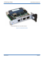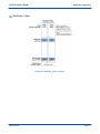
1
» VX3240 « 3U VPX Single Board Computer User's Guide CA.DT.B07-0e - July 2013 If it's embedded, it's Kontron. VX3240 User's Guide Preface Revision History Publication Title: VX3240 User's Guide Doc. ID: CA.DT.B07-0e Rev. 0e Brief Description of Changes Initial Version Date of Issue 07-2013 Copyright © 2013 Kontron AG. All rights reserved. All data is for information purposes only and not guaranteed for legal purposes. Information has been carefully checked and is believed to be accurate; however, no responsibility is assumed for inaccuracies. Kontron and the Kontron logo and all other trademarks or registered trademarks are the property of their respective owners and are recognized. Specifications are subject to change without notice. Page i CA.DT.B07-0e VX3240 User's Guide Preface Proprietary Note This document contains information proprietary to Kontron. It may not be copied or transmitted by any means, disclosed to others, or stored in any retrieval system or media without the prior written consent of Kontron or one of its authorized agents. The information contained in this document is, to the best of our knowledge, entirely correct. However, Kontron cannot accept liability for any inaccuracies or the consequences thereof, or for any liability arising from the use or application of any circuit, product, or example shown in this document. Kontron reserves the right to change, modify, or improve this document or the product described herein, as seen fit by Kontron without further notice. Trademarks This document may include names, company logos and trademarks, which are registered trademarks and, therefore, proprietary to their respective owners. Environmental Protection Statement This product has been manufactured to satisfy environmental protection requirements where possible. Many of the components used (structural parts, printed circuit boards, connectors, batteries, etc.) are capable of being recycled. Final disposition of this product after its service life must be accomplished in accordance with applicable country, state, or local laws or regulations. The Waste Electrical and Electronic Equipment (WEEE) Directive aims to: > reduce waste arising from electrical and electronic equipment (EEE) > make producers of EEE responsible for the environmental impact of their products, especially when they become waste > encourage separate collection and subsequent treatment, reuse, recovery, recycling and sound environmental disposal of EEE > improve the environmental performance of all those involved during the lifecycle of EEE CA.DT.B07-0e Page ii Preface VX3240 User's Guide Conventions This guide uses several types of notice: Note, Caution, ESD. Note: this notice calls attention to important features or instructions. Caution: this notice alert you to system damage, loss of data, or risk of personal injury. ESD: This banner indicates an Electrostatic Sensitive Device. All numbers are expressed in decimal, except addresses and memory or register data, which are expressed in hexadecimal. The prefix `0x' shows a hexadecimal number, following the `C' programming language convention. The multipliers `k', `M' and `G' have their conventional scientific and engineering meanings of *103, *106 and *109 respectively. The only exception to this is in the description of the size of memory areas, when `K', `M' and `G' mean *210, *220 and *230 respectively. When describing transfer rates, `k' `M' and `G' mean *103, *106 and *109 not *2 10 *2 20 and *2 30. In PowerPC terminology, multiple bit fields are numbered from 0 to n, where 0 is the MSB and n is the LSB. PCI and CompactPCI terminology follows the more familiar convention that bit 0 is the LSB and n is the MSB. Signal names ending with an asterisk (*) or a hash (#) denote active low signals; all other signals are active high. Signal names follow the PICMG 2.0 R3.0 CompactPCI Specification and the PCI Local Bus 2.3 Specification. For Your Safety Your new Kontron product was developed and tested carefully to provide all features necessary to ensure its compliance with electrical safety requirements. It was also designed for a long fault-free life. However, the life expectancy of your product can be drastically reduced by improper treatment during unpacking and installation. Therefore, in the interest of your own safety and of the correct operation of your new Kontron product, you are requested to conform with the following guidelines. High Voltage Safety Instructions Warning! All operations on this device must be carried out by sufficiently skilled personnel only. Caution, Electric Shock! Before installing a not hot-swappable Kontron product into a system always ensure that your mains power is switched off. This applies also to the installation of piggybacks. Serious electrical shock hazards can exist during all installation, repair and maintenance operations with this product. Therefore, always unplug the power cable and any other cables which provide external voltages before performing work. Page iii CA.DT.B07-0e VX3240 User's Guide Preface Special Handling and Unpacking Instructions ESD Sensitive Device! Electronic boards and their components are sensitive to static electricity. Therefore, care must be taken during all handling operations and inspections of this product, in order to ensure product integrity at all times Do not handle this product out of its protective enclosure while it is not used for operational purposes unless it is otherwise protected. Whenever possible, unpack or pack this product only at EOS/ESD safe work stations. Where a safe work station is not guaranteed, it is important for the user to be electrically discharged before touching the product with his/her hands or tools. This is most easily done by touching a metal part of your system housing. It is particularly important to observe standard anti-static precautions when changing piggybacks, ROM devices, jumper settings etc. If the product contains batteries for RTC or memory backup, ensure that the board is not placed on conductive surfaces, including anti-static plastics or sponges. They can cause short circuits and damage the batteries or conductive circuits on the board. General Instructions on Usage In order to maintain Kontron’s product warranty, this product must not be altered or modified in any way. Changes or modifications to the device, which are not explicitly approved by Kontron and described in this manual or received from Kontron’s Technical Support as a special handling instruction, will void your warranty. This device should only be installed in or connected to systems that fulfill all necessary technical and specific environmental requirements. This applies also to the operational temperature range of the specific board version, which must not be exceeded. If batteries are present, their temperature restrictions must be taken into account. In performing all necessary installation and application operations, please follow only the instructions supplied by the present manual. Keep all the original packaging material for future storage or warranty shipments. If it is necessary to store or ship the board, please re-pack it as nearly as possible in the manner in which it was delivered. Special care is necessary when handling or unpacking the product. Please consult the special handling and unpacking instruction on the previous page of this manual. CA.DT.B07-0e Page iv VX3240 User's Guide Table Of Contents Table Of Contents Chapter 1 - Introduction . . . . . . . . . . . . . . . . . . . . . . . . . . . . . . . . . . . . . . . . . . . . . . . . . . . . . . . . . . 1 1.1 Manual Overview . . . . . . . . . . . . . . . . . . . . . . . . . . . . . . . . . . . . . . . . . . . . . . . . . . . . . . . . . . . . . . . . . 1.1.1 Objectives . . . . . . . . . . . . . . . . . . . . . . . . . . . . . . . . . . . . . . . . . . . . . . . . . . . . . . . . . . . . . . . . . . . 1.1.2 Audience . . . . . . . . . . . . . . . . . . . . . . . . . . . . . . . . . . . . . . . . . . . . . . . . . . . . . . . . . . . . . . . . . . . . . 1.1.3 Scope . . . . . . . . . . . . . . . . . . . . . . . . . . . . . . . . . . . . . . . . . . . . . . . . . . . . . . . . . . . . . . . . . . . . . . . 1.1.4 Structure . . . . . . . . . . . . . . . . . . . . . . . . . . . . . . . . . . . . . . . . . . . . . . . . . . . . . . . . . . . . . . . . . . . . . 2 2 2 2 2 1.2 VPX Overview . . . . . . . . . . . . . . . . . . . . . . . . . . . . . . . . . . . . . . . . . . . . . . . . . . . . . . . . . . . . . . . . . . . 3 1.3 Board Overview . . . . . . . . . . . . . . . . . . . . . . . . . . . . . . . . . . . . . . . . . . . . . . . . . . . . . . . . . . . . . . . . . . 1.3.1 Main Features . . . . . . . . . . . . . . . . . . . . . . . . . . . . . . . . . . . . . . . . . . . . . . . . . . . . . . . . . . . . . . . . 1.3.2 Order Code Table . . . . . . . . . . . . . . . . . . . . . . . . . . . . . . . . . . . . . . . . . . . . . . . . . . . . . . . . . . . . . 1.3.3 I/O Interfaces . . . . . . . . . . . . . . . . . . . . . . . . . . . . . . . . . . . . . . . . . . . . . . . . . . . . . . . . . . . . . . . . . 3 3 5 5 1.4 Functional Block Diagram . . . . . . . . . . . . . . . . . . . . . . . . . . . . . . . . . . . . . . . . . . . . . . . . . . . . . . . . . . 1.4.1 VX3240 Components Layout . . . . . . . . . . . . . . . . . . . . . . . . . . . . . . . . . . . . . . . . . . . . . . . . . . . 7 8 1.5 9 Technical Specification . . . . . . . . . . . . . . . . . . . . . . . . . . . . . . . . . . . . . . . . . . . . . . . . . . . . . . . . . . . . 1.5.1 MTBF Data . . . . . . . . . . . . . . . . . . . . . . . . . . . . . . . . . . . . . . . . . . . . . . . . . . . . . . . . . . . . . . . . . . . 11 Software Support . . . . . . . . . . . . . . . . . . . . . . . . . . . . . . . . . . . . . . . . . . . . . . . . . . . . . . . . . . . . . . . . . 12 1.7 Standard . . . . . . . . . . . . . . . . . . . . . . . . . . . . . . . . . . . . . . . . . . . . . . . . . . . . . . . . . . . . . . . . . . . . . . . . 1.7.1 Environmental Specifications . . . . . . . . . . . . . . . . . . . . . . . . . . . . . . . . . . . . . . . . . . . . . . . . . . . 13 13 1.8 14 1.6 Related Publications . . . . . . . . . . . . . . . . . . . . . . . . . . . . . . . . . . . . . . . . . . . . . . . . . . . . . . . . . . . . . . Chapter 2 - Functional Description . . . . . . . . . . . . . . . . . . . . . . . . . . . . . . . . . . . . . . . . . . . . . . . . 15 2.1 Processor and System Memory . . . . . . . . . . . . . . . . . . . . . . . . . . . . . . . . . . . . . . . . . . . . . . . . . . . . 2.1.1 Processor . . . . . . . . . . . . . . . . . . . . . . . . . . . . . . . . . . . . . . . . . . . . . . . . . . . . . . . . . . . . . . . . . . . . 2.1.2 System Memory . . . . . . . . . . . . . . . . . . . . . . . . . . . . . . . . . . . . . . . . . . . . . . . . . . . . . . . . . . . . . . 15 15 16 2.2 PCI Express Bus . . . . . . . . . . . . . . . . . . . . . . . . . . . . . . . . . . . . . . . . . . . . . . . . . . . . . . . . . . . . . . . . . 17 2.3 Gigabit Ethernet interfaces . . . . . . . . . . . . . . . . . . . . . . . . . . . . . . . . . . . . . . . . . . . . . . . . . . . . . . . . . 17 2.4 USB Interfaces . . . . . . . . . . . . . . . . . . . . . . . . . . . . . . . . . . . . . . . . . . . . . . . . . . . . . . . . . . . . . . . . . . . 17 2.5 Serial Interfaces . . . . . . . . . . . . . . . . . . . . . . . . . . . . . . . . . . . . . . . . . . . . . . . . . . . . . . . . . . . . . . . . . . 17 2.6 Storage . . . . . . . . . . . . . . . . . . . . . . . . . . . . . . . . . . . . . . . . . . . . . . . . . . . . . . . . . . . . . . . . . . . . . . . . . 18 2.6.1 2.6.2 2.6.3 2.6.4 2.6.5 Flash Memory . . . . . . . . . . . . . . . . . . . . . . . . . . . . . . . . . . . . . . . . . . . . . . . . . . . . . . . . . . . . . . . . Serial EEPROMs . . . . . . . . . . . . . . . . . . . . . . . . . . . . . . . . . . . . . . . . . . . . . . . . . . . . . . . . . . . . . SPI EEPROM . . . . . . . . . . . . . . . . . . . . . . . . . . . . . . . . . . . . . . . . . . . . . . . . . . . . . . . . . . . . . . . . F-RAM . . . . . . . . . . . . . . . . . . . . . . . . . . . . . . . . . . . . . . . . . . . . . . . . . . . . . . . . . . . . . . . . . . . . . . Dual Serial ATA . . . . . . . . . . . . . . . . . . . . . . . . . . . . . . . . . . . . . . . . . . . . . . . . . . . . . . . . . . . . . . . 18 18 18 18 18 CPLD Features . . . . . . . . . . . . . . . . . . . . . . . . . . . . . . . . . . . . . . . . . . . . . . . . . . . . . . . . . . . . . . . . . . 18 2.8 I2C Buses . . . . . . . . . . . . . . . . . . . . . . . . . . . . . . . . . . . . . . . . . . . . . . . . . . . . . . . . . . . . . . . . . . . . . . . 2.8.1 Internal I2C Slaves . . . . . . . . . . . . . . . . . . . . . . . . . . . . . . . . . . . . . . . . . . . . . . . . . . . . . . . . . . . . 2.8.2 RTC . . . . . . . . . . . . . . . . . . . . . . . . . . . . . . . . . . . . . . . . . . . . . . . . . . . . . . . . . . . . . . . . . . . . . . . . . 19 19 19 2.7 Page v CA.DT.B07-0e VX3240 User's Guide 2.8.3 2.8.4 2.8.5 2.8.6 2.8.7 Chapter 3 - Table Of Contents VPD EEPROM . . . . . . . . . . . . . . . . . . . . . . . . . . . . . . . . . . . . . . . . . . . . . . . . . . . . . . . . . . . . . . . Thermal Sensors . . . . . . . . . . . . . . . . . . . . . . . . . . . . . . . . . . . . . . . . . . . . . . . . . . . . . . . . . . . . . . Voltage Sensors . . . . . . . . . . . . . . . . . . . . . . . . . . . . . . . . . . . . . . . . . . . . . . . . . . . . . . . . . . . . . . VX3240 VPX I2C interfaces . . . . . . . . . . . . . . . . . . . . . . . . . . . . . . . . . . . . . . . . . . . . . . . . . . . . GPIO Expander . . . . . . . . . . . . . . . . . . . . . . . . . . . . . . . . . . . . . . . . . . . . . . . . . . . . . . . . . . . . . . . Physical I/O . . . . . . . . . . . . . . . . . . . . . . . . . . . . . . . . . . . . . . . . . . . . . . . . . . . . . . . . . 19 20 22 22 22 23 3.1 Front Panel Connectors . . . . . . . . . . . . . . . . . . . . . . . . . . . . . . . . . . . . . . . . . . . . . . . . . . . . . . . . . . . 3.1.1 Serial Connector COM . . . . . . . . . . . . . . . . . . . . . . . . . . . . . . . . . . . . . . . . . . . . . . . . . . . . . . . . . 3.1.2 USB Connector . . . . . . . . . . . . . . . . . . . . . . . . . . . . . . . . . . . . . . . . . . . . . . . . . . . . . . . . . . . . . . . 3.1.3 Gigabit Ethernet Connectors . . . . . . . . . . . . . . . . . . . . . . . . . . . . . . . . . . . . . . . . . . . . . . . . . . . . 23 23 24 25 3.2 Front Panel Leds . . . . . . . . . . . . . . . . . . . . . . . . . . . . . . . . . . . . . . . . . . . . . . . . . . . . . . . . . . . . . . . . . 26 3.3 Onboard Connectors . . . . . . . . . . . . . . . . . . . . . . . . . . . . . . . . . . . . . . . . . . . . . . . . . . . . . . . . . . . . . . 3.3.1 VPX Bus Interface . . . . . . . . . . . . . . . . . . . . . . . . . . . . . . . . . . . . . . . . . . . . . . . . . . . . . . . . . . . . 3.3.1.1 Board Connectors Identification . . . . . . . . . . . . . . . . . . . . . . . . . . . . . . . . . . . . . . 3.3.1.2 VPX Connectors Description . . . . . . . . . . . . . . . . . . . . . . . . . . . . . . . . . . . . . . . . 3.3.2 P0 Connector . . . . . . . . . . . . . . . . . . . . . . . . . . . . . . . . . . . . . . . . . . . . . . . . . . . . . . . . . . . . . . . . . 3.3.3 P1 Connector . . . . . . . . . . . . . . . . . . . . . . . . . . . . . . . . . . . . . . . . . . . . . . . . . . . . . . . . . . . . . . . . . 3.3.4 P2 Connector . . . . . . . . . . . . . . . . . . . . . . . . . . . . . . . . . . . . . . . . . . . . . . . . . . . . . . . . . . . . . . . . . 3.3.5 COP Header Connector . . . . . . . . . . . . . . . . . . . . . . . . . . . . . . . . . . . . . . . . . . . . . . . . . . . . . . . . 3.3.6 JTAG Connector . . . . . . . . . . . . . . . . . . . . . . . . . . . . . . . . . . . . . . . . . . . . . . . . . . . . . . . . . . . . . . 3.3.7 NAND Flash Connector . . . . . . . . . . . . . . . . . . . . . . . . . . . . . . . . . . . . . . . . . . . . . . . . . . . . . . . . 27 27 28 28 29 30 33 34 34 35 Chapter 4 - Installation . . . . . . . . . . . . . . . . . . . . . . . . . . . . . . . . . . . . . . . . . . . . . . . . . . . . . . . . . . . 36 4.1 Safety Requirements . . . . . . . . . . . . . . . . . . . . . . . . . . . . . . . . . . . . . . . . . . . . . . . . . . . . . . . . . . . . . . 36 4.2 Board Identification . . . . . . . . . . . . . . . . . . . . . . . . . . . . . . . . . . . . . . . . . . . . . . . . . . . . . . . . . . . . . . . 37 4.3 Board Configuration - Microswitches . . . . . . . . . . . . . . . . . . . . . . . . . . . . . . . . . . . . . . . . . . . . . . . . 4.3.1 DIP Switch SW1 Description . . . . . . . . . . . . . . . . . . . . . . . . . . . . . . . . . . . . . . . . . . . . . . . . . . . . 4.3.2 DIP Switch SW2 Description . . . . . . . . . . . . . . . . . . . . . . . . . . . . . . . . . . . . . . . . . . . . . . . . . . . . 38 38 39 4.4 Package Content . . . . . . . . . . . . . . . . . . . . . . . . . . . . . . . . . . . . . . . . . . . . . . . . . . . . . . . . . . . . . . . . . 40 4.5 Initial Installation Procedures . . . . . . . . . . . . . . . . . . . . . . . . . . . . . . . . . . . . . . . . . . . . . . . . . . . . . . . 41 4.6 Standard Removal Procedure . . . . . . . . . . . . . . . . . . . . . . . . . . . . . . . . . . . . . . . . . . . . . . . . . . . . . . 42 4.7 Installation of Peripheral Devices . . . . . . . . . . . . . . . . . . . . . . . . . . . . . . . . . . . . . . . . . . . . . . . . . . . 4.7.1 SATA Nand Flash Mezzanine Installation . . . . . . . . . . . . . . . . . . . . . . . . . . . . . . . . . . . . . . . . . 4.7.2 Battery Replacement . . . . . . . . . . . . . . . . . . . . . . . . . . . . . . . . . . . . . . . . . . . . . . . . . . . . . . . . . . 43 43 45 4.8 47 Software Installation . . . . . . . . . . . . . . . . . . . . . . . . . . . . . . . . . . . . . . . . . . . . . . . . . . . . . . . . . . . . . . Chapter 5 - Power Considerations . . . . . . . . . . . . . . . . . . . . . . . . . . . . . . . . . . . . . . . . . . . . . . . . 5.1 System Power . . . . . . . . . . . . . . . . . . . . . . . . . . . . . . . . . . . . . . . . . . . . . . . . . . . . . . . . . . . . . . . . . . . 5.1.1 VX3240 . . . . . . . . . . . . . . . . . . . . . . . . . . . . . . . . . . . . . . . . . . . . . . . . . . . . . . . . . . . . . . . . . . . . . . 5.1.2 Backplane . . . . . . . . . . . . . . . . . . . . . . . . . . . . . . . . . . . . . . . . . . . . . . . . . . . . . . . . . . . . . . . . . . . . 5.1.3 Power Supply Units . . . . . . . . . . . . . . . . . . . . . . . . . . . . . . . . . . . . . . . . . . . . . . . . . . . . . . . . . . . 5.1.3.1 Start-Up Requirement . . . . . . . . . . . . . . . . . . . . . . . . . . . . . . . . . . . . . . . . . . . . . . CA.DT.B07-0e 48 48 48 48 49 49 Page vi VX3240 User's Guide Table Of Contents 5.1.3.2 5.1.3.3 5.1.3.4 5.1.3.5 5.2 Power-Up Sequence . . . . . . . . . . . . . . . . . . . . . . . . . . . . . . . . . . . . . . . . . . . . . . . Tolerance . . . . . . . . . . . . . . . . . . . . . . . . . . . . . . . . . . . . . . . . . . . . . . . . . . . . . . . . . Regulation . . . . . . . . . . . . . . . . . . . . . . . . . . . . . . . . . . . . . . . . . . . . . . . . . . . . . . . . Rise Time Diagram . . . . . . . . . . . . . . . . . . . . . . . . . . . . . . . . . . . . . . . . . . . . . . . . . 49 50 50 51 Power Consumption . . . . . . . . . . . . . . . . . . . . . . . . . . . . . . . . . . . . . . . . . . . . . . . . . . . . . . . . . . . . . . 52 5.2.1 5.2.2 Chapter 6 - VX3240 Thermal Power . . . . . . . . . . . . . . . . . . . . . . . . . . . . . . . . . . . . . . . . . . . . . . . . . . . . . . . . VX3240 Maximum Current . . . . . . . . . . . . . . . . . . . . . . . . . . . . . . . . . . . . . . . . . . . . . . . . . . . . . VX3240-RTM Characteristics . . . . . . . . . . . . . . . . . . . . . . . . . . . . . . . . . . . . . . . . . . 52 53 54 6.1 Overview . . . . . . . . . . . . . . . . . . . . . . . . . . . . . . . . . . . . . . . . . . . . . . . . . . . . . . . . . . . . . . . . . . . . . . . . 54 6.2 Technical Specifications . . . . . . . . . . . . . . . . . . . . . . . . . . . . . . . . . . . . . . . . . . . . . . . . . . . . . . . . . . . 56 6.3 RTM Configuration . . . . . . . . . . . . . . . . . . . . . . . . . . . . . . . . . . . . . . . . . . . . . . . . . . . . . . . . . . . . . . . 57 6.4 Connectors . . . . . . . . . . . . . . . . . . . . . . . . . . . . . . . . . . . . . . . . . . . . . . . . . . . . . . . . . . . . . . . . . . . . . . 6.4.1 RTM Connectors Identification . . . . . . . . . . . . . . . . . . . . . . . . . . . . . . . . . . . . . . . . . . . . . . . . . . 6.4.2 Front Panel Connectors . . . . . . . . . . . . . . . . . . . . . . . . . . . . . . . . . . . . . . . . . . . . . . . . . . . . . . . . 6.4.3 Onboard Connectors . . . . . . . . . . . . . . . . . . . . . . . . . . . . . . . . . . . . . . . . . . . . . . . . . . . . . . . . . . 58 58 58 59 6.5 Modules Interfaces . . . . . . . . . . . . . . . . . . . . . . . . . . . . . . . . . . . . . . . . . . . . . . . . . . . . . . . . . . . . . . . 6.5.1 COM Interfaces . . . . . . . . . . . . . . . . . . . . . . . . . . . . . . . . . . . . . . . . . . . . . . . . . . . . . . . . . . . . . . 6.5.2 USB Interfaces . . . . . . . . . . . . . . . . . . . . . . . . . . . . . . . . . . . . . . . . . . . . . . . . . . . . . . . . . . . . . . . 6.5.3 Gigabit Ethernet Interfaces . . . . . . . . . . . . . . . . . . . . . . . . . . . . . . . . . . . . . . . . . . . . . . . . . . . . . 6.5.4 Serial ATA Interfaces . . . . . . . . . . . . . . . . . . . . . . . . . . . . . . . . . . . . . . . . . . . . . . . . . . . . . . . . . . 6.5.5 GPIO Connector . . . . . . . . . . . . . . . . . . . . . . . . . . . . . . . . . . . . . . . . . . . . . . . . . . . . . . . . . . . . . . 6.5.6 JTAG Connector . . . . . . . . . . . . . . . . . . . . . . . . . . . . . . . . . . . . . . . . . . . . . . . . . . . . . . . . . . . . . . 6.5.7 I2C System Management Connector . . . . . . . . . . . . . . . . . . . . . . . . . . . . . . . . . . . . . . . . . . . . . 61 61 62 65 66 67 68 69 6.6 Reset . . . . . . . . . . . . . . . . . . . . . . . . . . . . . . . . . . . . . . . . . . . . . . . . . . . . . . . . . . . . . . . . . . . . . . . . . . . 70 6.7 Power Consideration . . . . . . . . . . . . . . . . . . . . . . . . . . . . . . . . . . . . . . . . . . . . . . . . . . . . . . . . . . . . . . 70 6.8 Rear I/O Interfaces 6.8.1 RP2 Connector 6.8.2 RP1 Connector 6.8.3 RP0 Connector ............................................................... ............................................................... ............................................................... ............................................................... 71 72 73 75 6.9 PCI 64 PIM Connector . . . . . . . . . . . . . . . . . . . . . . . . . . . . . . . . . . . . . . . . . . . . . . . . . . . . . . . . . . . . 6.9.1 J10 Connector . . . . . . . . . . . . . . . . . . . . . . . . . . . . . . . . . . . . . . . . . . . . . . . . . . . . . . . . . . . . . . . . 6.9.2 J14 Connector . . . . . . . . . . . . . . . . . . . . . . . . . . . . . . . . . . . . . . . . . . . . . . . . . . . . . . . . . . . . . . . . 77 77 78 Chapter 7 - Page vii Backplane Suggestions . . . . . . . . . . . . . . . . . . . . . . . . . . . . . . . . . . . . . . . . . . . . . . . 79 CA.DT.B07-0e VX3240 User's Guide Table Of Contents List Of Figures Figure 1: VX3240-SA Overview . . . . . . . . . . . . . . . . . . . . . . . . . . . . . . . . . . . . . . . . . . . . . . . . . . . . . . . . . . . . 1 Figure 2: VX3240 Functional Block Diagrams . . . . . . . . . . . . . . . . . . . . . . . . . . . . . . . . . . . . . . . . . . . . . . . . 7 Figure 3: VX3240 Components Layout (Top View) . . . . . . . . . . . . . . . . . . . . . . . . . . . . . . . . . . . . . . . . . . . . 8 Figure 4: VX3240 Board Components Layout (Bottom View) . . . . . . . . . . . . . . . . . . . . . . . . . . . . . . . . . . . 8 Figure 5: QorIQ™ P2041 Block Diagram . . . . . . . . . . . . . . . . . . . . . . . . . . . . . . . . . . . . . . . . . . . . . . . . . . . . 16 Figure 6: I2C Buses . . . . . . . . . . . . . . . . . . . . . . . . . . . . . . . . . . . . . . . . . . . . . . . . . . . . . . . . . . . . . . . . . . . . . . 19 Figure 7: Location of Board and Processor Sensors . . . . . . . . . . . . . . . . . . . . . . . . . . . . . . . . . . . . . . . . . . . 21 Figure 8: Front Panel Connectors Layout . . . . . . . . . . . . . . . . . . . . . . . . . . . . . . . . . . . . . . . . . . . . . . . . . . . . 23 Figure 9: Serial Connector . . . . . . . . . . . . . . . . . . . . . . . . . . . . . . . . . . . . . . . . . . . . . . . . . . . . . . . . . . . . . . . . . 23 Figure 10: USB Connector . . . . . . . . . . . . . . . . . . . . . . . . . . . . . . . . . . . . . . . . . . . . . . . . . . . . . . . . . . . . . . . . . 24 Figure 11: Dual Gigabit Ethernet Connector . . . . . . . . . . . . . . . . . . . . . . . . . . . . . . . . . . . . . . . . . . . . . . . . . . 25 Figure 12: Front Panel LEDs . . . . . . . . . . . . . . . . . . . . . . . . . . . . . . . . . . . . . . . . . . . . . . . . . . . . . . . . . . . . . . . 26 Figure 13: VX3240 Connectors Layout (top) . . . . . . . . . . . . . . . . . . . . . . . . . . . . . . . . . . . . . . . . . . . . . . . . . . 27 Figure 14: VPX Connectors . . . . . . . . . . . . . . . . . . . . . . . . . . . . . . . . . . . . . . . . . . . . . . . . . . . . . . . . . . . . . . . . 27 Figure 15: Connector Identification for 3U VPX Board . . . . . . . . . . . . . . . . . . . . . . . . . . . . . . . . . . . . . . . . . 28 Figure 16: COP Header . . . . . . . . . . . . . . . . . . . . . . . . . . . . . . . . . . . . . . . . . . . . . . . . . . . . . . . . . . . . . . . . . . . 34 Figure 17: JTAG Connector . . . . . . . . . . . . . . . . . . . . . . . . . . . . . . . . . . . . . . . . . . . . . . . . . . . . . . . . . . . . . . . . 34 Figure 18: NAND Flash Connector . . . . . . . . . . . . . . . . . . . . . . . . . . . . . . . . . . . . . . . . . . . . . . . . . . . . . . . . . . 35 Figure 19: VX3240 Identification (Top Side) . . . . . . . . . . . . . . . . . . . . . . . . . . . . . . . . . . . . . . . . . . . . . . . . . . 37 Figure 20: Board Configuration . . . . . . . . . . . . . . . . . . . . . . . . . . . . . . . . . . . . . . . . . . . . . . . . . . . . . . . . . . . . . 38 Figure 21: SATA Mezzanine Slot Location . . . . . . . . . . . . . . . . . . . . . . . . . . . . . . . . . . . . . . . . . . . . . . . . . . . 43 Figure 22: Flash Memory Module Installation . . . . . . . . . . . . . . . . . . . . . . . . . . . . . . . . . . . . . . . . . . . . . . . . . 44 Figure 23: NAND Flash Disk Overview . . . . . . . . . . . . . . . . . . . . . . . . . . . . . . . . . . . . . . . . . . . . . . . . . . . . . . 44 Figure 24: Battery Life . . . . . . . . . . . . . . . . . . . . . . . . . . . . . . . . . . . . . . . . . . . . . . . . . . . . . . . . . . . . . . . . . . . . 45 Figure 25: Battery Socket . . . . . . . . . . . . . . . . . . . . . . . . . . . . . . . . . . . . . . . . . . . . . . . . . . . . . . . . . . . . . . . . . 46 Figure 26: Start-Up Ramp of the CP3-SVE180 AC Power Supply . . . . . . . . . . . . . . . . . . . . . . . . . . . . . . . 51 Figure 27: VX3240-RTM Overview . . . . . . . . . . . . . . . . . . . . . . . . . . . . . . . . . . . . . . . . . . . . . . . . . . . . . . . . . . 55 Figure 28: VX3240-RTM MicroSwitch Location . . . . . . . . . . . . . . . . . . . . . . . . . . . . . . . . . . . . . . . . . . . . . . . 57 Figure 29: Connector Identification for 3U RTM . . . . . . . . . . . . . . . . . . . . . . . . . . . . . . . . . . . . . . . . . . . . . . . 58 Figure 30: VX3240-RTM Front Panel Connectors . . . . . . . . . . . . . . . . . . . . . . . . . . . . . . . . . . . . . . . . . . . . . 58 Figure 31: VX3240-RTM Onboard Connectors (PB-VX3-001) . . . . . . . . . . . . . . . . . . . . . . . . . . . . . . . . . . 59 Figure 32: Serial Port Connector . . . . . . . . . . . . . . . . . . . . . . . . . . . . . . . . . . . . . . . . . . . . . . . . . . . . . . . . . . . 61 Figure 33: Front Panel USB Connector . . . . . . . . . . . . . . . . . . . . . . . . . . . . . . . . . . . . . . . . . . . . . . . . . . . . . . 62 Figure 34: Onboard USB Connector . . . . . . . . . . . . . . . . . . . . . . . . . . . . . . . . . . . . . . . . . . . . . . . . . . . . . . . . 63 Figure 35: USB Flash Disk Overview . . . . . . . . . . . . . . . . . . . . . . . . . . . . . . . . . . . . . . . . . . . . . . . . . . . . . . . . 63 Figure 36: USB Flash Disk Layout . . . . . . . . . . . . . . . . . . . . . . . . . . . . . . . . . . . . . . . . . . . . . . . . . . . . . . . . . . 64 Figure 37: Gigabit Ethernet Connectors . . . . . . . . . . . . . . . . . . . . . . . . . . . . . . . . . . . . . . . . . . . . . . . . . . . . . 65 CA.DT.B07-0e Page viii Table Of Contents VX3240 User's Guide Figure 38: Onboard SATA Connectors . . . . . . . . . . . . . . . . . . . . . . . . . . . . . . . . . . . . . . . . . . . . . . . . . . . . . . 66 Figure 39: Onboard GPIO Connector . . . . . . . . . . . . . . . . . . . . . . . . . . . . . . . . . . . . . . . . . . . . . . . . . . . . . . . 67 Figure 40: Onboard JTAG Connector . . . . . . . . . . . . . . . . . . . . . . . . . . . . . . . . . . . . . . . . . . . . . . . . . . . . . . . 68 Figure 41: Onboard JTAG Connector . . . . . . . . . . . . . . . . . . . . . . . . . . . . . . . . . . . . . . . . . . . . . . . . . . . . . . . 69 Figure 42: VX3240-RTM Reset Push Button . . . . . . . . . . . . . . . . . . . . . . . . . . . . . . . . . . . . . . . . . . . . . . . . . 70 Figure 43: Rear I/O VPX Connectors . . . . . . . . . . . . . . . . . . . . . . . . . . . . . . . . . . . . . . . . . . . . . . . . . . . . . . . . 71 Figure 45: Single Star x4, 8 SlotsTopology . . . . . . . . . . . . . . . . . . . . . . . . . . . . . . . . . . . . . . . . . . . . . . . . . . . 79 Figure 46: Single Star x4, 5 Slots Topology . . . . . . . . . . . . . . . . . . . . . . . . . . . . . . . . . . . . . . . . . . . . . . . . . . 80 Figure 47: Distributed, 2 Slots Topology . . . . . . . . . . . . . . . . . . . . . . . . . . . . . . . . . . . . . . . . . . . . . . . . . . . . . 81 Page ix CA.DT.B07-0e VX3240 User's Guide Table Of Contents List Of Tables Table 1: Order Code . . . . . . . . . . . . . . . . . . . . . . . . . . . . . . . . . . . . . . . . . . . . . . . . . . . . . . . . . . . . . . . . . . . . . . 5 Table 2: Front I/O Interfaces . . . . . . . . . . . . . . . . . . . . . . . . . . . . . . . . . . . . . . . . . . . . . . . . . . . . . . . . . . . . . . . 5 Table 3: Rear I/O Interfaces . . . . . . . . . . . . . . . . . . . . . . . . . . . . . . . . . . . . . . . . . . . . . . . . . . . . . . . . . . . . . . . 6 Table 4: VX3240 Main Specifications . . . . . . . . . . . . . . . . . . . . . . . . . . . . . . . . . . . . . . . . . . . . . . . . . . . . . . . 11 Table 5: VX3240-SAA1N-000 MTBF Data . . . . . . . . . . . . . . . . . . . . . . . . . . . . . . . . . . . . . . . . . . . . . . . . . . . 11 Table 6: Standards . . . . . . . . . . . . . . . . . . . . . . . . . . . . . . . . . . . . . . . . . . . . . . . . . . . . . . . . . . . . . . . . . . . . . . . 13 Table 7: Environmental Specifications . . . . . . . . . . . . . . . . . . . . . . . . . . . . . . . . . . . . . . . . . . . . . . . . . . . . . . . 13 Table 8: Related Publications . . . . . . . . . . . . . . . . . . . . . . . . . . . . . . . . . . . . . . . . . . . . . . . . . . . . . . . . . . . . . . 14 Table 9: Serial Connector Pin Assignment . . . . . . . . . . . . . . . . . . . . . . . . . . . . . . . . . . . . . . . . . . . . . . . . . . . 23 Table 10: Serial Connector Signal Description . . . . . . . . . . . . . . . . . . . . . . . . . . . . . . . . . . . . . . . . . . . . . . . . 23 Table 11: USB Connector Pin Assignment . . . . . . . . . . . . . . . . . . . . . . . . . . . . . . . . . . . . . . . . . . . . . . . . . . . 24 Table 12: Gigabit Ethernet Connectors ETH0 and ETH1 Pin Assignment . . . . . . . . . . . . . . . . . . . . . . . . 25 Table 13: VPX Connector P0 Wafer Assignment . . . . . . . . . . . . . . . . . . . . . . . . . . . . . . . . . . . . . . . . . . . . . . 29 Table 14: VPX Connector P0 Signal Definition . . . . . . . . . . . . . . . . . . . . . . . . . . . . . . . . . . . . . . . . . . . . . . . . 29 Table 15: VPX Connector P1 Wafer Assignment . . . . . . . . . . . . . . . . . . . . . . . . . . . . . . . . . . . . . . . . . . . . . . 30 Table 16: VPX Connector P1 Signal Definition . . . . . . . . . . . . . . . . . . . . . . . . . . . . . . . . . . . . . . . . . . . . . . . . 31 Table 17: USB Port Features . . . . . . . . . . . . . . . . . . . . . . . . . . . . . . . . . . . . . . . . . . . . . . . . . . . . . . . . . . . . . . 31 Table 18: Ethernet Port Features . . . . . . . . . . . . . . . . . . . . . . . . . . . . . . . . . . . . . . . . . . . . . . . . . . . . . . . . . . . 32 Table 19: SATA Port Features . . . . . . . . . . . . . . . . . . . . . . . . . . . . . . . . . . . . . . . . . . . . . . . . . . . . . . . . . . . . . 32 Table 20: VPX Connector P2 Wafer Assignment . . . . . . . . . . . . . . . . . . . . . . . . . . . . . . . . . . . . . . . . . . . . . . 33 Table 21: VPX Connector P2 Signal Definition . . . . . . . . . . . . . . . . . . . . . . . . . . . . . . . . . . . . . . . . . . . . . . . . 33 Table 22: COP Header Pin Assignment . . . . . . . . . . . . . . . . . . . . . . . . . . . . . . . . . . . . . . . . . . . . . . . . . . . . . 34 Table 23: JTAG Connector Pin Assignment . . . . . . . . . . . . . . . . . . . . . . . . . . . . . . . . . . . . . . . . . . . . . . . . . . 34 Table 24: NAND Flash Connector Pin Assignment . . . . . . . . . . . . . . . . . . . . . . . . . . . . . . . . . . . . . . . . . . . . 35 Table 25: SW1 Mircroswitch Description . . . . . . . . . . . . . . . . . . . . . . . . . . . . . . . . . . . . . . . . . . . . . . . . . . . . . 38 Table 26: SW2 Mircroswitch Description . . . . . . . . . . . . . . . . . . . . . . . . . . . . . . . . . . . . . . . . . . . . . . . . . . . . . 39 Table 27: DC Operational Input Voltage Ranges . . . . . . . . . . . . . . . . . . . . . . . . . . . . . . . . . . . . . . . . . . . . . . 48 Table 28: Input Voltage Characteristics . . . . . . . . . . . . . . . . . . . . . . . . . . . . . . . . . . . . . . . . . . . . . . . . . . . . . . 50 Table 29: Thermal Power . . . . . . . . . . . . . . . . . . . . . . . . . . . . . . . . . . . . . . . . . . . . . . . . . . . . . . . . . . . . . . . . . . 52 Table 30: Maximum Current . . . . . . . . . . . . . . . . . . . . . . . . . . . . . . . . . . . . . . . . . . . . . . . . . . . . . . . . . . . . . . . 53 Table 31: Order Code . . . . . . . . . . . . . . . . . . . . . . . . . . . . . . . . . . . . . . . . . . . . . . . . . . . . . . . . . . . . . . . . . . . . . 54 Table 32: VX3240-RTM Main Specifications . . . . . . . . . . . . . . . . . . . . . . . . . . . . . . . . . . . . . . . . . . . . . . . . . 56 Table 33: Serial Port Connector Pin Assignment . . . . . . . . . . . . . . . . . . . . . . . . . . . . . . . . . . . . . . . . . . . . . . 61 Table 34: Front Panel USB Connector Pin Assignment . . . . . . . . . . . . . . . . . . . . . . . . . . . . . . . . . . . . . . . . 62 Table 35: Onboard USB Connector Pin Assignment . . . . . . . . . . . . . . . . . . . . . . . . . . . . . . . . . . . . . . . . . . . 63 Table 36: Gigabit Ethernet Connectors Pin Assignment . . . . . . . . . . . . . . . . . . . . . . . . . . . . . . . . . . . . . . . . 65 Table 37: Onboard SATA Connectors Pin Assignment . . . . . . . . . . . . . . . . . . . . . . . . . . . . . . . . . . . . . . . . . 66 CA.DT.B07-0e Page x Table Of Contents VX3240 User's Guide Table 38: Onboard GPIO Connector Pin Assignment . . . . . . . . . . . . . . . . . . . . . . . . . . . . . . . . . . . . . . . . . . 67 Table 39: Onboard JTAG Connector Pin Assignment . . . . . . . . . . . . . . . . . . . . . . . . . . . . . . . . . . . . . . . . . . 68 Table 40: Onboard I2C Connector Pin Assignment . . . . . . . . . . . . . . . . . . . . . . . . . . . . . . . . . . . . . . . . . . . . 69 Table 41: Rear I/O VPX Connector RP2 Wafer Assignment . . . . . . . . . . . . . . . . . . . . . . . . . . . . . . . . . . . . 72 Table 42: Rear I/O VPX Connector RP2 Signal Definition . . . . . . . . . . . . . . . . . . . . . . . . . . . . . . . . . . . . . . 72 Table 43: Rear I/O VPX Connector RP1 Wafer Assignment . . . . . . . . . . . . . . . . . . . . . . . . . . . . . . . . . . . . 73 Table 44: Rear I/O VPX Connector RP1 Signal Definition . . . . . . . . . . . . . . . . . . . . . . . . . . . . . . . . . . . . . . 74 Table 45: Rear I/O VPX Connector RP0 Wafer Assignment . . . . . . . . . . . . . . . . . . . . . . . . . . . . . . . . . . . . 75 Table 46: Rear I/O VPX Connector RP0 Signal Definition . . . . . . . . . . . . . . . . . . . . . . . . . . . . . . . . . . . . . . 76 Page xi CA.DT.B07-0e Introduction VX3240 User's Guide Chapter 1 - Introduction VX3240 is a low-power 3U VPX SBC featuring a quad-core Freescale P2041 QorIQ™ device with quad PowerPC e500mc cores at 1.2 GHz. VX3240 supports up to 8 GB DDR-3 SDRAM and provides a wide range of I/Os including Gigabit Ethernet, GPIOs, PMC/XMC I/Os, USB, SATA and serial ports. With such a features set, the VX3240 is the ideal general purpose solution for SWaP-C constrained embedded applications. Coupled with Kontron Long Term Supply policy, VX3240 is the perfect migration path to a new 10+ year period of deploy ments for PowerPC-based applications in the Military, Aerospace and Transportation markets. In this document, the term: VX3240 > VX3240-SA VX3240-RTM refers to the 3U VPX board refers to the standard commercial version of the board. refers to the 3U VPX Rear Transition Module (RTM). Figure 1: VX3240-SA Overview CA.DT.B07-0e Page 1 Introduction 1.1 1.1.1 VX3240 User's Guide Manual Overview Objectives This guide provides general information, hardware preparation and installation instructions, operating instructions and a functional description of the VX3240 board. The onboard programming, onboard firmware and other software (e.g. drivers and BSPs) are described in detail in separate guides (see section 1.8 “Related Publications"). As the standard policy for all the Kontron, hardware technical documentation reflects the most recent version of our products. The “Hardware Release Notes" (see section 1.8 “Related Publications") is to help to keep track of various evolutions that have happened during the early steps of the VX3240 ramp-up or later in its lifetime. Functional changes that differ from previous version of the document are identified by a vertical bar in the margin. 1.1.2 Audience This guide is written to cover, as far as possible, the range of people who will handle or use the VX3240, from unpackers/inspectors, through system managers and installation technicians to hardware and software engineers. Most chapters assume a certain amount of knowledge on the subjects of single board computer architecture, interfaces, peripherals, systems, cabling, grounding and communications. 1.1.3 Scope This guide describes all variants of the VX3240 series. It does not cover any PMC modules which are described in specific guides (see section 1.8 “Related Publications"). 1.1.4 Structure This guide is structured in a way that will reflect the sequence of operations from receipt of the board up to getting it working in your system. Each topic is covered in a separate chapter and each chapter begins with a brief introduction that tells you what the chapter contains. In this way, you can skip any chapters that are not applicable or with which you are already familiar. The chapters are: > Chapter 1 - Introduction (this chapter) > Chapter 2 - Functional Description > Chapter 3 - Physical I/O > Chapter 4 - Installation > Chapter 5 - Power Considerations > Chapter 6 - VX3240-RTM Characteristics > Chapter 7 - Backplane Suggestions Page 2 CA.DT.B07-0e VX3240 User's Guide 1.2 Introduction VPX Overview VPX (VITA 46) specifications establish a new direction for the next revolution in bus boards. VPX is a proposed ANSI standard which breaks out from the traditional connector scheme of VMEbus to merge the latest in connector and packaging technology with the latest in bus and serial fabric technology. VPX combines best-inclass technologies to assure a very long technology cycle similar to that of the original VMEbus solutions. Traditional parallel VMEbus will continue to be supported by VPX through bridging schemes that assure a solid migration pathway. For further information regarding this standards and its use, visit the home page of the VITA - Open Standards, Open Markets. 1.3 1.3.1 Board Overview Main Features Freescale QorIQ™ P2041 Architecture The VX3240 3U VPX SBC is based on the Freescale QorIQ™ P2041 integrated host processor, clocked at 1.2GHz. The QorIQ™ P2041 combines four e500mc processor cores built on Power Architecture® technology with highperformance data path acceleration architecture (DPAA), CoreNet fabric infrastructure, as well as network and peripheral bus interfaces required for networking, Telecom/datacom, wireless infrastructure, and military/ aerospace applications. The QorIQ™ P2041 is a flexible device that can be configured to meet many system application needs. The P2041's e500mc cores can be combined as a fully-symmetric, multiprocessing, system-on-a-chip, or they can be operated with varying degrees of independence to perform asymmetric multiprocessing. Full processor independence, including the ability to independently boot and reset each core, is a defining characteristic of the QorIQ™ P2041. The ability of the cores to run different operating systems, or run OS-less, provides the user with significant flexibility in partitioning between control, datapath, and applications processing. It also simplifies consolidation of functions previously spread across multiple discrete processors onto a single device. The QorIQ™ P2041 offers four high-performance 32-bit e500mc cores built on Power Architecture® technology. Like previous e500 cores, each e500mc is a superscalar dual issue processor, supporting out-of-order execution and in-order completion, which allows the e500mc core built on Power Architecture® technology to perform more instructions per clock than other RISC and CISC architectures. Soldered DDR3 Memories with the Support of ECC The QorIQ™ P2041 accesses one memory-channel having a total size of 2, 4 or 8 GB. The DDR3 memory technology used operates at 1066 Gbits/s. The resulting peak memory bandwidth is 8.5 GB/s. An 8 bits ECC memory is implemented to detect and correct errors. CA.DT.B07-0e Page 3 Introduction VX3240 User's Guide Numerous Storage Interface The following storage features are available: 4 An onboard or mezzanine SATA NAND Flash with 32 GB capacity (Multiple Levels Cell) or 8 GB capacity (Single Level Cell extended temperature). 4 Dual redundant 128 MB NOR flash memory is used to store firmware code. 4 Two serial 256 Kbits EEPROMs are dedicated to system and application data storage. 4 A 1 Mbits ferroelectric, non-volatile random access memory allows the backup of critical data when the board is powered off. This 1 Mbits ferroelectric RAM is a user memory device. One SATA gen1 and one USB 2.0 port available on the P1 backplane connector. Backplane Switch Available on P1 connector: 4 Two compliant VITA 31.1 Gigabit Ethernet links, 4 One 4x PCI Express gen 2 link without Non Transparent (NT) capability. Extensive I/O Connectivity The VX3240 provides two 10/100/1000BASE-TX Ethernet interfaces, two EIA-232 serial lines, two general purpose I/Os, two USB 2.0 links, two SATA interfaces and one 4x PCI-Express link. Software The VX3240 is delivered with the OpenSource U-Boot firmware. The VX3240 supports the OpenSource YOCTO Project Poky Danny 1.3 release (http://git.yoctoproject.org/cgit/ cgit.cgi/poky/refs/tags) used together with the Freescale PowerPC layer (http://git.yoctoproject.org/cgit/cgit.cgi/ meta-fsl-ppc/) which generates a 3.0.48-r10 Linux kernel. Kontron has a meta-vx3240 layer which further refines this development kit specifically for the VX3240 board. Harsh Environments The VX3240 has been designed using the same PCB for both air and conduction-cooled boards. Builds variants span a complete range of temperature, shock and vibration requirements as specified in the VITA 47 standards. Rear Transition Module The VX3240 supports the PB-VX3-001, a 3U VPX Rear Transition Module compliant with the definition of the Rear Transistion Module on VPX standard - VITA 46.10. It offers connectivity on the rear for: 4 One USB 2.0 port 4 Two Gigabit Ethernet ports without LED signals 4 Two COM (Serial) ports 4 One SATA gen 2 port 4 Two GPIOs 4 One Reset button 4 One System Management Bus Connector 4 One JTAG connector Page 4 CA.DT.B07-0e Introduction VX3240 User's Guide 1.3.2 Order Code Table Available order codes are listed in table below: Article Order Code Description 3U VPX Air-Cooled Commercial Build SBC VX3240-SA VX3240-SAC2-00000 VX3240 Air-Cooled Commercial Build, QorIQ P2041 1.2 GHz, 2 GB DDR3SDRAM, no Sata Flash (MLC) on board, no XMC/PMC slot, 1000BASE-T Ethernet interfaces Associated Products VX3240-RTM PB-VX3-001 VX3240 VPX Rear Transition Module (no PIM connector), 10/100/1000BASE-TX Ethernet interfaces COP/JTAG Module COP-PN3-B COP JTAG Equipment Serial Cable Serial Cable Adapter KIT-RJ12DB9 Table 1: Order Code 1.3.3 I/O Interfaces Front Interfaces FUNCTION DESCRIPTION Gigabit Ethernet Two 1000BASE-T ports on RJ-45 connectors Serial One RJ-12 connector for EIA-232 simplified UART interface (with RTS/CTS) USB One USB 2.0 port on 4-pin standard USB connector LEDs Three LEDs reporting the board CPU health status and activity Reset Board Reset Button Table 2: Front I/O Interfaces CA.DT.B07-0e Page 5 Introduction VX3240 User's Guide Rear Interfaces FUNCTION DESCRIPTION VPX VPX standard on P0/P1/P2 Gigabit Ethernet Two Gigabit Ethernet ports on P1 PCI Express PCI Express x4 on P1 (VITA 46.4) Serial Two simplified EIA-232 interfaces on P2 (with RTS/CTS) USB One USB 2.0 port on P1 SATA One SATA II port on P1 Reset Main reset input available on P0 connector GPIOs 2 User GPIOs on P1 and 3 additional GPIOs on P0 SMB 2x System Management Bus on P0 Table 3: Rear I/O Interfaces Page 6 CA.DT.B07-0e Introduction VX3240 User's Guide 1.4 Functional Block Diagram The following diagrams provide additional information concerning board functionalities and components layout. Figure 2: VX3240 Functional Block Diagrams CA.DT.B07-0e Page 7 Introduction 1.4.1 VX3240 User's Guide VX3240 Components Layout Optional SATA NAND Mezzanine Header Battery Optional SATA NAND Flash Freescale QorIQ™ P2041 DDR3 Figure 3: VX3240 Components Layout (Top View) Microswitch SW1 Boot Flash Microswitch SW2 ETH PHY ETH PHY DDR3 Figure 4: VX3240 Board Components Layout (Bottom View) Page 8 CA.DT.B07-0e Introduction VX3240 User's Guide 1.5 Technical Specification VX3240 SPECIFICATIONS Form Factor Form Factor VPX 3U, single slot 0.8” Processor and Chipset Processor Freescale QorIQ™ P2041 (quad e500mc core) @ 1.2 GHz. Cache Structure L1 cache: 32 KB Data + 32 KB Instruction L2 cache:128 KB, CPCache: 1024KB Gigabit Ethernet Controller Three on-chip, triple-speed Ethernet controllers supporting 10 Mbps, 100Mbps and 1 Gbps Ethernet/IEEE®802.3 networks with SGMII utilization. Memory Controller Integrated DDR3 memory controller with ECC support, up to 1200 MHz, 72-bit. SATA Up to 3 Gb/s integrated Serial ATA host controllers on up to 2 ports. One SATA link on VPX P1 and one for onboard SSD Disk. USB Two Enhanced Host Controllers Interface (EHCI) that allow data transfers up to 480 Mb/s. One USB link on front panel or rear panel P1 and one on rear panel P1 only. UARTs 2 x UART, 16550-style, 4-wires. PCI Express One x4 Gen2 link (5Gbps) Memory System Memory One single bank 2 GB DDR3 SDRAM @1200 MHz, 64-bit wide + ECC, soldered. Firmware Boot device 128 MB soldered NOR flash for U-Boot, redundant boot device (2 x 64 MB partition) SSD SATA Disk Up to 32 GB (MLC technology) SSD SATA disk SATA Nand Flash storage on socket (for SATA Nand Flash modules) or directly onboard. FRAM 1 Mbit F-RAM on SPI (default) or I2C (spare option) EEPROM 1 x serial 256 Kbit EEPROM dedicated to DDR data (spare EEPROM for SPD) 1 x serial 256 Kbit EEPROM dedicated to system data (VPD) 1 x serial 256 Kbit EEPROM dedicated to application data 1 x serial 256 Kbit EEPROM dedicated to firmware boot (spare EEPROM) 1 x serial 256 Kbit EEPROM dedicated for board date (spare EEPROM) SPI Two 64 Mbit flashes CA.DT.B07-0e Page 9 Introduction VX3240 User's Guide VX3240 SPECIFICATIONS Onboard Controllers Watchdog No watchdog controller. RTC I²C Real Time Clock, RV-8564-C2 from Micro-Crystal Switzerland. Gigabit Ethernet PHY Three Marvell 88E1112 transceivers with SerDes and Copper media interface. System cPLD Board controller for power sequencing control, reset generation and distribution, monitoring, system clock configuration and flash booting bank selection. Also provides configuration/status registers on local bus processor interface. Hardware Monitoring Temperature (LM73) and Voltage (NCT7802Y) sensors. GPIO Expander I²C GPIO Expander PCA9672. System Rear Intectonnection Gigabit Ethernet Two 1000BASE-T on P1 switchable on front panel by microswitches (onboard LAN switch). PCI Express x4 Gen2 (5 Gbps) PCI Express on P1. USB Port One (default) or two high-speed USB Port on P1. SATA Port One SATA Port on P1. Serial Ports Two EIA-232 Serial Ports on P2. GPIOs Three GPIOs on P0. Two GPIOs on P1. Front Interfaces Gigabit Ethernet Two 1000BASE-T on RJ-45 connectors switchable on rear panel by microswitches (on board LAN switch). Serial Port One EIA-232 Serial Port on RJ-12 connector. USB Port One USB connector Reset Reset button LEDs 5 bicolor LEDs. Various Interfaces Debug Interface Page 10 JTAG/COP port for emulation probe connection. CA.DT.B07-0e Introduction VX3240 User's Guide VX3240 SPECIFICATIONS MISC Battery BR1225 on board socket. Firmware U-Boot Backplane Power Supply VS1 (+12V), VS3 (+5V) inputs fully protected by fuse. VS2 (+3V3) not used. +3V3 SB optional. +12V SB and -12V SB not used. Operating temperature Range 0.8” SA: 0°C to +55ºC with passive module heat sink, forced system airflow (1.8m/s to 3 m/s depending on the processor heatsink) Humidity 0-90% non-condensing (SA), 95% Coated. Board Weight SA environment class: 250g with heatsink Table 4: VX3240 Main Specifications For a detailed description of the VX3240-RTM (Rear Transition Module), refer to the Technical Specifications table in Chapter 6 “ VX3240-RTM Characteristics", section 6.2 “Technical Specifications" page 56. 1.5.1 MTBF Data Calculations are made according to the standard MIL-HDBK217F-2 for following types of environment: > Ground Benign (GB) > Air Inhabited Cargo (AIC) > Naval Sheltered (NS), > Air Rotary Wing (ARW) VX3240-SAA1N-000 GB (Hours) VX3240/SA AIC (Hours) NS (Hours) ARW (Hours) IEC62380 25°C 40°C 40°C 25°C 40°C 55°C Typical Railway Mission Profile 318 426h 228 653h 31696h 51 971h 41 492h 8 237h 341 175h Table 5: VX3240-SAA1N-000 MTBF Data CA.DT.B07-0e Page 11 Introduction 1.6 VX3240 User's Guide Software Support Kontron is one of the few cPCI, VME and VPX vendors providing inhouse support for most of the industry-proven real-time operating systems that are currently available. Due to its close relationship with the software manufacturers, Kontron is able to produce and support BSPs and drivers for the latest operating system revisions thereby taking advantage of the changes in technology. Finally, customers possessing a maintenance agreement with Kontron can be guaranteed hotline software support and are supplied with regular software updates. A dedicated web site is also provided for online updates and release downloads. The VX3240 can operate under the following operating system: > Linux Please contact Kontron for further information concerning other operating systems and software support. Page 12 CA.DT.B07-0e Introduction VX3240 User's Guide 1.7 Standard This Kontron product complies with the requirements of the following standards. TYPE CE ASPECT DESCRIPTION Emission EN55022 EN61000-6-3 Immission EN55024 EN61000-6-2 Electrical Safety EN60950-1 Mechanical Mechanical Dimensions IEEE1101.10 Environmental WEEE Waste electrical and electronic equipment RoHS Restriction of the use of certain hazardous substances in electrical and electronic equipment Table 6: Standards 1.7.1 Environmental Specifications SA - Standard Commercial Conformal Coating Optional Airflow 2 m/s Temperature VITA 47-Class AC1 Cooling Method Convection Operating 0°C to +55°C Storage -45°C to +85°C Vibration Sine (Operating) 2g / 20-500 Hz acceleration / frequency range Random VITA 47-Class V1 Shock (Operating) 20g / 11 ms peak accel. / shock duration half sine Altitude (Operating) -1,640 to 60,000 ft Relative Humidity 90% non-condensing (95% with coating option) Table 7: Environmental Specifications CA.DT.B07-0e Page 13 Introduction 1.8 VX3240 User's Guide Related Publications The following publications contain information relating to this product: PRODUCT PUBLICATION VX3240 Boards VX3240 Hardware Release Notes VX3240 U-Boot User Manual CA.DT.B10 (not yet available) SD.DT.xxx (not yet available) EZ3-VX3240 Systems EZ3-VX3240-00-L Quick Start EZ3-VX3240 Getting Started - SD.DT.xxx (not yet available) SD.DT.xxx (not yet available) Serial ATA Serial ATA 2.0 Specification VITA 46.0 VPX Base Standard - ANSI/VITA 46.0-2007 VITA 46.4 PCI Express® on VPX Fabric Connector - VITA Draft Standard VITA 46.6 Gigabit Ethernet Control Plane on VPX - VITA Draft Standard VITA 46.10 Rear Transition Module on VPX - ANSI-VITA 46.10-2009 Table 8: Related Publications Page 14 CA.DT.B07-0e Functional Description VX3240 User's Guide Chapter 2 2.1 2.1.1 Functional Description Processor and System Memory Processor The QorIQ™ P2041 SoC includes the following functions and features: > Four e500mc cores built on Power Architecture technology cache. P2041 also supports 128-Kbyte private backside cache for each of the cores. 4 Three levels of instructions: user, supervisor, and hypervisor 4 Independent boot and reset 4 Secure boot capability > 1-Mbyte shared CoreNet platform cache (CPC) 4 Hierarchical interconnect fabric 4 CoreNet fabric supporting coherent and non-coherent transactions with prioritization and bandwidth allocation amongst CoreNet end-points 4 Queue manager fabric supporting packet-level queue management and quality of service scheduling > One 64-bit DDR3/3L SDRAM memory controller with ECC and chip-select interleaving support > Data path acceleration architecture incorporating acceleration for the following functions: 4 Packet parsing, classification, and distribution 4 Queue Management for scheduling, packet sequencing, and congestion management 4 Hardware Buffer Management for buffer allocation and de-allocation 4 Encryption/decryption (SEC 4.2) 4 RegEx Pattern Matching (PME 2.1) 4 RapidIO messaging manager (RMan) > Ethernet interfaces 4 Five 1 Gbps or four 2.5 Gbps Ethernet controllers. P2041 also supports a 10 Gbps Ethernet (XAUI) Controller > High speed peripheral interfaces 4 Three PCI Express 2.0 controllers/ports running at up to 5 Gbps 4 Two serial RapidIO controllers/ports version 1.3 with features of 2.1 running at up to 5 Gbps 4 RapidIO message manager (RMan) with Type 5-6 and Type 8-11 support 4 Dual SATA 2.0 interfaces supporting 1.5 and 3.0 Gbps operation > Additional peripheral interfaces 4 Two USB 2.0 controllers with integrated PHY 4 SD/MMC controller (eSDHC) 4 Enhanced SPI controller 4 Four I2C controllers 4 Dual DUARTs CA.DT.B07-0e Page 15 Functional Description > > > > VX3240 User's Guide Ten SerDes lanes to 5 GHz Enhanced local bus controller (eLBC) Multicore programmable interrupt controller (PIC) Two 4-channel DMA engines Figure 5: QorIQ™ P2041 Block Diagram 2.1.2 System Memory The VX3240 supports a single-channel (72-bit), registered Double Data Rate (DDR3) memory with Error Che cking and Correcting (ECC). > The DDR3 interface operates at a rate up to 1066 Gbits/s resulting in a peak bandwidth of 8.5 GB/s. > The available memory configurations are 2 GB, 4 GB or 8 GB.. > Using ECC, the P2041 detects and corrects all single-bit errors, and detects all double-bit errors and all errors within a nibble. Page 16 CA.DT.B07-0e VX3240 User's Guide 2.2 Functional Description PCI Express Bus The VX3240 provides one x4 PCI Express link directly routed to VPX P1. The PCI Express bus interface operates up to 5 Gbps on each lane resulting in a peak bandwith of 500 MB/s per lane (500 MB/s on RX way and 500 MB/S on TX way). The resulting bandwidth for the x4 PCI Express link is 2 GB/s (4x 500 MB/s) per way. The VX3240 does not support PCI Express Non Transparent (NT) mode for PCIe backplane links. The VX3240 should not be used as a Peripheral board. 2.3 Gigabit Ethernet interfaces The QorIQ™ P2041 integrates two triple-speed Ethernet controllers which are associated on the VX3240 board with two external Marvell 88E1112 Ethernet PHY. The Ethernet channels 0 and 1 can either be routed to: 4 The front panel RJ-45 connectors, 4 The VPX P1 connector, thanks to the use of Lan Switch. 2.4 USB Interfaces The VX3240 provides two USB 2.0 ports. 4 One USB port is available on the front panel. 4 One USB port is available on VPX P1 connector. Each port provides a +5V output to power external USB devices such as keyboards. On the USB 2.0 Rear I/O ports, it is strongly recommended to use a cable below 3 meters in length for USB 2.0 devices. The USB 2.0 ports are high-speed, full-speed, and low-speed capable. Hi-speed USB 2.0 allows data transfers of up to 480 Mb/s - 40 times faster than a full-speed USB (USB 1.1). 2.5 Serial Interfaces The VX3240 integrates two serial communications ports, COM1 and COM2 in PC parlance. COM1 and COM2 are available via the VPX P2 connector. COM1 is also available via the front panel connector. 4 COM1: EIA-232 (simplified RX/TX) port on RJ-12 front panel connector or on the rear P2 connector 4 COM2: EIA-232 (simplified RX/TX) port on the rear P2 connector Default serial mode is EIA-232, 115200 bauds. CA.DT.B07-0e Page 17 Functional Description 2.6 2.6.1 VX3240 User's Guide Storage Flash Memory The VX3240 provides one 128 MB flash device. This flash device (NOR flash) is organized in two partitions of 64 MB which operate as redundant boot devices. The selection of the active boot flash partitions is controlled by a DIP switch. 2.6.2 Serial EEPROMs There are two 256-kbit onboard serial EEPROMS: 4 One serial 256 Kbit EEPROM dedicated to system data. 4 One serial 256 Kbit EEPROM dedicated to application data. 2.6.3 SPI EEPROM There are two 64-Mbit onboard SPI Flashes. 2.6.4 F-RAM A 1-Mbit SPI F-RAM (Ferroelectric Nonvolatile RAM) provides fast, non-volatile storage of mission state data not to be lost when power is removed. F-RAM combines the nonvolatile data storage capability of ROM with the benefits of RAM, which includes a high number of read and write cycles (100 Trillion), high speed read and write cycles, and low power consumption. 2.6.5 Dual Serial ATA The QorIQ™ P2041 provides two Serial ATA 2.0 (3 Gbps) interfaces. 4 One SATA port is available on VPX P1 connector. Refer to section 3.3.1.2 “VPX Connector Description ”page 28 for more information on P1 wafer assignment. 4 One SATA port is available either on optional SATA NAND Flash or optional SATA NAND Flash Mezzanine header 2.7 CPLD Features The CPLD manages the following features: 4 Power-on/off control 4 Reset control 4 Local environmental control/monitoring 4 Local Bus interface to processor 4 LEDs control 4 Internal registers that allow system management Page 18 CA.DT.B07-0e Functional Description VX3240 User's Guide 2.8 2.8.1 I2C Buses Internal I2C Slaves The I2C buses controller allows interfacing to a wide number of 2-wire serial standards based on the original I2C concepts. The controller has four multi-master I2C buses (Master and Slave). The master interface is used to drive commands on to the I2C and get responses from other devices. The slave section monitors the I2C and will accept commands that are addressed to it. The slave section can also be put in a monitoring mode, where it will report all activity on the bus but not respond. Figure 6: I2C Buses 2.8.2 RTC The VX3240 RTC is based on the RV-8564-C2 CMOS real-time clock/calendar optimized for low power consumption (-40 °C / +85 °C). This RTC provides a programmable clock output, interrupt output and voltage low detector. An internal timer is also available. All address/data are transferred serially via the I2C bus, at a maximal spped of 400 Kbit/s. The built-in word address register is incremented automatically after each writing or read data byte. The VX3240 RTC includes a built-in crystal oscillating at 32.768 MHz. Crystal accuracy across temperature: -160 ppm at -40 °C, 0 ppm at 25 °C, -140 ppm at +85 °C. The RTC is connected to the first I2C controller inside the QorIQ™ P2041 at I2C hardware address A2H. Nominal operating voltage 3V3. Minimal clock operating voltage 1.2V A 3V RTC backup battery, BR1225 can be equipped in a keystone socket. This battery supports extended tem perature range. 2.8.3 VPD EEPROM One M24C256 eeprom (256 kb serial eeprom) contains Vital Product Data. This memory is organized as 8192x8 bits. CA.DT.B07-0e Page 19 Functional Description 2.8.4 VX3240 User's Guide Thermal Sensors To ensure optimal and long-term reliability of the VX3240, all onboard components must remain within the maxi mum temperature specifications. The most critical components on the VX3240 are the processor and the memory. Operating the VX3240 above the maximum operating limits will result in permanent damage to the board. Three thermal sensors, located on the I2C bus, are available on the VX3240. > ZL6100 CPU sensor: the CPU core temperature is monitored by a Intersil ZL6100ALAF device, at I2C hardware address 22H. This device uses remote sensing on CPU thermal diode and also indicates local board temperature. This sensor temperature is dedicated to junction processor temperature and checks only maximal Tj temperature. Key features: 4 Local temperature accuracy: +/- 3 °C 4 Remote temperature accuracy: +/- 0.75 °C 4 Operating temperature: -40°C / +125 °C > LM73 board sensor: the board temperature on Top face is monitored by a LM73 device, at I2C hardware address 90H. Key features: 4 Local temperature accuracy: +/- 2 °C (-40 °C to +150 °C) 4 Operating temperature: -40 °C / +150 °C > NCT7802Y board sensor: the board temperature on Bottom face is monitored by a Nuvoton NCT7802Y device, at I2C hardware address 50H. Key features: 4 Local temperature accuracy: +/- 2°C (25°C to +70°C) 4 Operating temperature: -40°C / +85°C Page 20 CA.DT.B07-0e Functional Description VX3240 User's Guide LM73 Board Sensor ZL6100 CPU Sensor NCT7802Y Tempe rature and Voltage Sensor Figure 7: Location of Board and Processor Sensors CA.DT.B07-0e Page 21 Functional Description 2.8.5 VX3240 User's Guide Voltage Sensors The NCT7802Y, at I2C hardware address 50H, is a Nuvoton Hardware Monitor IC, wich can monitor power supply voltages and temperatures. Key features: 4 Voltage monitoring accuracy: +/- 10 mV 4 Analog Input VSEN1: DDR Memory 1.5V 4 Analog Input VSEN2: VPX VS1 12V 4 Analog Input VSEN3: VPX VS3 5V 4 Analog Input VCORE: CPU Core 1.05V 2.8.6 VX3240 VPX I2C interfaces VX3240 implements two I2C buses connected to P0 VPX connector (refer to section 3.3.2 page 29 - P0 pin assignments) 4 I2C0: CLK signal on pin P0/B5, DATA signal on pin P0/A5 4 I2C1: CLK signal on pin P0/G4, DATA signal on pin P0/F4 2.8.7 GPIO Expander The VX3240 implements a GPIO Expander NXP PCA9672PW, at I2C hardware address 44H, which drives GPIO1 to GPIO5 connected to P0 and P1 VPX connectors (refer to sections 3.3.2 page 29 and 3.3.3 page 30 – P0 and P1 pin assignments ) The PCA9672PW has a sinking current capability of 25 mA per GPIO. In applications requiring additional drive, two port pins may be connected together to sink up to 50 mA current. Both bits must then always be turned on or off together. Page 22 CA.DT.B07-0e Physical I/O VX3240 User's Guide Chapter 3 - 3.1 Physical I/O Front Panel Connectors COM1 USB Gigabit Ethernet ETH0 ETH1 Reset Figure 8: Front Panel Connectors Layout 3.1.1 Serial Connector COM Pin Assignment PIN SIGNAL 1 RTS 2 Shell 3 TXD 4 RXD 5 GND 6 CTS Pin 1 Table 9: Serial Connector Pin Assignment MNEMONIC Pin 6 Figure 9: Serial Connector DESCRIPTION CTS EIA-232 Clear-To-Send RTS EIA-232 Ready-To-Send RXD EIA-232Receive Data TXD EIA-232 Transmit Data GND Ground Shell Chassis Ground Table 10: Serial Connector Signal Description CA.DT.B07-0e Page 23 Physical I/O VX3240 User's Guide Serial Cable Designation Serial cable is: 4 RJ-14 (6 pin, 4 conductor) for a simple EIA-232 without handshake support. 4 RJ-12 (6 pin, 6 conductor) for EIA-232 with handshaking. A RJ-12 to DB9/DB25 male or DB9/DB25 female adapter is available from multiple sources, such as: - Kontron Order Code KIT-RJ12DB9 - Triangle Cable http://www.trianglecables.com/db9m-rj12.html Pin Connector DB9 Pin Connector RJ-12 Signal 1 RTS 1 2 TXD 3 3 RXD 4 4 CTS 6 5 GND 5 3.1.2 RJ-12 cable DB9 female adapter USB Connector Pin Assignment PIN SIGNAL FUNCTION I/O 1 VCC (1) VCC 2 USB_D- Differential USB- I/O 3 USB_D+ Differential USB+ I/O 4 GND GND Table 11: USB Connector Pin Assignment -- 4 1 -- Figure 10: USB Connector +5V protected power up to 1A continuous, short circuit current limited (1A max.) with thermal shutdown, and automatic restart when short is removed. (1) Page 24 CA.DT.B07-0e Physical I/O VX3240 User's Guide 3.1.3 Gigabit Ethernet Connectors Pin Assignment 10BASE-T 100BASE-TX 1000BASE-T PIN I/O SIGNAL I/O SIGNAL I/O SIGNAL 1 O TX+ O TX+ I/O BI_DA+ 2 O TX- O TX- I/O BI_DA- 3 I RX+ I RX+ I/O BI_DB+ 4 - - - - I/O BI_DC+ 5 - - - - I/O BI_DC- 6 I TX- I RX- I/O BI_DB- 7 - - - - I/O BI_DD+ 8 - - - - I/O BI_DD- Shell Chassis Ground Gigabit Ethernet ETH0 ETH1 1 8 1 8 Figure 11: Dual Gigabit Ethernet Connector Table 12: Gigabit Ethernet Connectors ETH0 and ETH1 Pin Assignment The Ethernet transmission can operate effectively using a CAT5 cable with a maximum length of 100 m. The Ethernet connectors are available as RJ-45 connectors with tab down. The interfaces provide automatic detection and switching between 10Base-T, 100Base-TX and 1000Base-T data transmission (Auto-Negotiation). Auto-wire switching for crossed cables is also supported (Auto-MDI/X). CA.DT.B07-0e Page 25 Physical I/O 3.2 VX3240 User's Guide Front Panel Leds L1 Reset L2 L3 L4 L5 Figure 12: Front Panel LEDs Status LEDs Default Settings CPU LED L1 L2 L3 L4 L5 Page 26 DESCRIPTION COLOR RED Thermal Alert GREEN Card power OK, not in reset state RED CPU Checkstop GREEN Local Bus Activity RED Reserved for future use GREEN Reserved for future use RED ETH0 - On: Link 10. GREEN ETH0 - On: Link 1000. Blink: Activity RED + GREEN ETH0 - On: Link 100. Blink: Activity RED ETH1 - On: Link 10. Blink: Activity GREEN ETH1 - On: Link 1000. Blink: Activity RED + GREEN ETH1 - On: Link 100. Blink: Activity Blink: Activity CA.DT.B07-0e Physical I/O VX3240 User's Guide 3.3 Onboard Connectors CN4 CN5 P0 P1 P2 CN3 Figure 13: VX3240 Connectors Layout (top) 3.3.1 VPX Bus Interface The complete VPX connector configuration comprises three connectors named P0, P1 and P2 > P0: one 8-wafer 7-row connector > P1: one 16-wafer 7-row connector > P2: one 16-wafer 7-row connector The VX3240 is not hot-swappable but supports the addition or removal of other boards whilst in a powered-up state. The VX3240 is designed for a VPX bus architecture. P2 16 P1 1 16 P0 1 8 1 Figure 14: VPX Connectors CA.DT.B07-0e Page 27 Physical I/O VX3240 User's Guide 3.3.1.1 Board Connectors Identification Alignment/Keying Sockets P0 P1 P2 Alignment/Keying Pins Figure 15: Connector Identification for 3U VPX Board 3.3.1.2 VPX Connectors Description The VX3240 is provided with three VPX bus connectors, P0, P1 and P2 The VX3240 board provides Rear I/O connectivity for special compact systems. When the Rear I/O module is used, the signals may be routed to the Rear I/O module interface. Thus the Rear I/O module makes it much easier to remove the CPU in the rack as there is practically no cabling on the CPU board. The VX3240 Rear I/O provides the following interfaces: > Three GPIOs P0 > One USB 2.0 ports P1 > Two Gigabit Ethernet ports without LED signals P1 > One SATA ports P1 > Two GPIOs P1 > x4 or x1 PCI-Express P1 > Two EIA-232 COM ports P2 Page 28 CA.DT.B07-0e Physical I/O VX3240 User's Guide 3.3.2 P0 Connector P0 Wafer Assignment Wafer ROW G ROW F ROW E ROW D ROW C ROW B ROW A 1 VS1 VS1 VS1 N.C. NC (VS2) NC (VS2) NC (VS2) 2 VS1 VS1 VS1 N.C. NC (VS2) NC (VS2) NC (VS2) 3 VS3 VS3 VS3 N.C. VS3 VS3 VS3 4 I2C1_CLK I2C1_DAT GND NC (-12V_AUX) GND SYSRESET* NVMRO 5 GAP* GA4* GND 3V3_AUX GND I2C0_CLK I2C0_DAT 6 GA3* GA2* GND NC (+12V_AUX) GND GA1* GA0* 7 GPIO5 (TCK) GND Reserved Reserved GND GPIO3 (TMS) GPIO4 (TRST*) 8 GND Reserved Reserved GND Reserved Reserved GND CASE GND * signal active when low Table 13: VPX Connector P0 Wafer Assignment P0 Signal Definition MNEMONIC SIGNAL DEFINITION 3V3_AUX +3.3 Volts auxiliary power GA0* to GA4* Geographical Address Inputs 0-4 GAP Geographical Address Parity GND Ground GPIOx General purpose I/O I2C0 I2C Bus 0 I2C1 I2C Bus 1 N.C. Not Connected NVMRO Non-Volatile Memory Read Only. When asserted (logical 1), prevents any non-volatile memory from being updated. SYSRESET* System Reset. Input and open collector output. VS1 +12 Volts DC power (VS1 VPX supply) VS3 +5 Volts DC power (VS3 VPX supply) Table 14: VPX Connector P0 Signal Definition CA.DT.B07-0e Page 29 Physical I/O 3.3.3 VX3240 User's Guide P1 Connector P1 Wafer Assignment > Legend for Table 15: P1_VBAT Battery Voltage USB USB P1_SYS_CON* System Controller SATA Serial ATA Port PCIe L0-RX | L0-TX x4 PCI-Express ETHx Gigabit Ethernet Port Wafer ROW G ROW F ROW E ROW D ROW C ROW B ROW A 1 Reserved GND PCIe L0-TX- PCIe L0-TX+ GND PCIe L0-RX- PCIe L0-RX+ 2 GND PCIe L1-TX- PCIe L1-TX+ GND PCIe L1-RX- PCIe L1-RX+ GND 3 VBAT GND PCIe L2-TX- PCIe L2-TX+ GND PCIe L2-RX- PCIe L2-RX+ 4 GND PCIe L3-TX- PCIe L3-TX+ GND PCIe L3-RX- PCIe L3-RX+ GND 5 SYS_CON* GND Reserved Reserved GND Reserved Reserved 6 GND Reserved Reserved GND Reserved Reserved GND 7 Reserved GND Reserved Reserved GND Reserved Reserved 8 GND Reserved Reserved GND Reserved Reserved GND 9 USB PWR GND SATA TX+ GND SATA RX- SATA RX+ 10 GND Reserved Reserved GND Reserved Reserved GND 11 Reserved GND Reserved Reserved GND Reserved Reserved 12 GND USB D- USB D+ GND Reserved Reserved GND 13 GPIO1 GND ETH1 DB- ETH1 DB+ GND ETH1 DA- ETH1 DA+ 14 GND ETH1 DD- ETH1 DD+ GND ETH1 DC- ETH1 DC+ GND 15 GPIO2 GND ETH0 DB- ETH0 DB+ GND ETH0 DA- ETH0 DA+ 16 GND ETH0 DD- ETH0 DD+ GND ETH0 DC- ETH0 DC+ GND CASE SATA TX- GND * signal active when low Table 15: VPX Connector P1 Wafer Assignment Page 30 CA.DT.B07-0e Physical I/O VX3240 User's Guide P1 Signal Definition MNEMONIC SIGNAL DEFINITION ETHx DA+/- 10/100/1000BASE-TX Ethernet x: First pair of Transmit/Receive data. ETHx DB+/- 10/100/1000BASE-TX Ethernet x: Second pair of Transmit/Receive data. ETHx DC+/- 10/100/1000BASE-TX Ethernet x: Third pair of Transmit/Receive data. ETHx DD+/- 10/100/1000BASE-TX Ethernet x: Fourth pair of Transmit/Receive data. GND Ground GPIOx General Purpose I/O x PCIe Lx-RX+/- x4 PCI Express Link - Receive +/- Lane x PCIe Lx-TX+/- x4 PCI Express Link - Transmit +/- Lane x Reserved Reserved SATA RX+/- Serial ATA Receive +/- SATA TX+/- Serial ATA Transmit +/- SYS_CON* System Controller Slot Indication USB D+/- Differential Data Pair of USB link USB PWR USB Power VBAT Battery Voltage Input, 3V. Optional alternated source for RTC backup voltage Table 16: VPX Connector P1 Signal Definition > USB Interfaces There are up to two independent USB interfaces available as described below: USB PORT CONNECTOR USAGE USB0 USB on the VX3240 (front panel) External USB devices USB1 USB on the VX3240-RTM (front panel) External USB devices Table 17: USB Port Features All USB ports may be used at the same time. It is strongly recommended to use cables less than 3 meters in length for the Rear I/O interfaces. CA.DT.B07-0e Page 31 Physical I/O VX3240 User's Guide > Ethernet Interfaces Gigabit Ethernet signals are available on the Rear I/O interface (ETH0 and ETH1 in above Table). Ethernet PORT CONNECTOR ETH0 ETH0 on the VX3240 (front panel) or CN12-R on the VX3240-RTM (front panel) ETH1 ETH1 on the VX3240 (front panel) or CN13-R on the VX3240-RTM Table 18: Ethernet Port Features > SATA Interface The VX3240 provides two SATA interfaces (SATA0 and SATA1 in above Table). SATA0 can be used only on the Rear I/O interface, SATA1 is used for the onboard SATA NAND Flash module or mezzanine. All SATA ports can be used simultaneously. SATA PORT USAGE CONNECTOR SATA0 CN14-R on the VX3240-RTM External SATA HDD drives, e.g. 2.5" or 3.5" SATA HDDs SATA1 CN5 on the VX3240 (optional) SATA Nand Flash Module Table 19: SATA Port Features Page 32 CA.DT.B07-0e Physical I/O VX3240 User's Guide 3.3.4 P2 Connector P2 Wafer Assignment > Legend for Table 20: COMx COM port Wafer Row G Row F Row E Row D Row C Row B Row A 1 COM1 RTS GND Reserved Reserved GND Reserved Reserved 2 GND Reserved Reserved GND Reserved Reserved GND 3 COM1 TXD GND Reserved Reserved GND Reserved Reserved 4 GND Reserved Reserved GND Reserved Reserved GND 5 COM1 CTS GND Reserved Reserved GND Reserved Reserved 6 GND Reserved Reserved GND Reserved Reserved GND 7 COM1 RXD GND Reserved Reserved GND Reserved Reserved 8 GND Reserved Reserved GND Reserved Reserved GND 9 COM2 RTS GND Reserved Reserved GND Reserved Reserved 10 GND Reserved Reserved GND Reserved Reserved GND 11 COM2 TXD GND Reserved Reserved GND Reserved Reserved 12 GND Reserved Reserved GND Reserved Reserved GND 13 COM2 CTS GND Reserved Reserved GND Reserved Reserved 14 GND Reserved Reserved GND Reserved Reserved GND 15 COM2 RXD GND Reserved Reserved GND Reserved Reserved 16 GND Reserved Reserved GND Reserved Reserved GND CASE GND Table 20: VPX Connector P2 Wafer Assignment P2 Signal Definition MNEMONIC SIGNAL DEFINITION COMx CTS Channel EIA-232 x Clear To Send COMx RTS Channel EIA-232 x Ready To Send COMx RXD Channel EIA-232 x Receive Data COMx TXD Channel EIA-232 x Transmit Data GND Ground Table 21: VPX Connector P2 Signal Definition CA.DT.B07-0e Page 33 Physical I/O 3.3.5 VX3240 User's Guide COP Header Connector COP Header Signal Definition The COP connector (Common On-chip Processor) can be utilized by external toolsets or testers to perform board-level validation, test and debug applications. Pin Mnemonic Signal Definition 1 TDO Test Data Out 2 N.C. Not Connected 3 TDI Test Data In 4 TRST* Test Reset 5 N.C. Not Connected 6 VCC +3.3 Volts DC Probe Sense 7 TCK Test Clock 8 CHKSTP_IN* CPU Checkstop In 9 TMS Test Mode Select 10 N.C. Not Connected 11 SRESET* COP Software Reset 12 N.C. Not Connected 13 HRESET* COP Hardware Reset 14 Key Pin Not Connected 15 CHKSTP_OUT* CPU Checkstop Out GND Ground 16 * CN4 Figure 16: COP Header Signals active when low. Table 22: COP Header Pin Assignment 3.3.6 JTAG Connector JTAG Signal Definition The CPLD is programmed via the JTAG (CN3) connector. The CPLD is the only device on the JTAG chain. Pin Mnemonic Signal Definition 1 TCK Test Clock 2 GND Ground 3 TDO Test Data Out 4 VCC +3.3 Volts DC Probe Sense 5 TMS Test Mode Select 6 N.C. Not Connected 7 N.C. Not Connected 8 N.C. Not Connected 9 TDI Test Data In 10 GND Ground CN3 Figure 17: JTAG Connector Table 23: JTAG Connector Pin Assignment Page 34 CA.DT.B07-0e Physical I/O VX3240 User's Guide 3.3.7 NAND Flash Connector NAND Flash Signal Definition Pin Mnemonic Signal Definition 1 PWR +5 Volts DC Mezzanine Power Supply 2 SATA RX+ Serial ATA. Receive plus. 3 N.C. Not Connected 4 SATA RX- Serial ATA. Receive minus. 5 N.C. Not Connected 6 GND Ground 7 GND Ground 8 SATA TX+ Serial ATA. Transmit plus. 9 N.C. Not Connected 10 SATA TX- Serial ATA. Transmit minus 9 1 10 2 Figure 18: NAND Flash Connector Table 24: NAND Flash Connector Pin Assignment CA.DT.B07-0e Page 35 Installation Chapter 4 - VX3240 User's Guide Installation The VX3240 has been designed for easy installation. However, the following standard precautions, installation procedures, and general information must be observed to ensure proper installation and to preclude damage to the board, other system components, or injury to personnel. 4.1 Safety Requirements The following safety precautions must be observed when installing or operating the VX3240. Kontron assumes no responsibility for any damage resulting from failure to comply with these requirements. Due care should be exercised when handling the board due to the fact that the heat sink can get very hot. Do not touch the heat sink when installing or removing the board. In addition, the board should not be placed on any surface or in any form of storage container until such time as the board and heat sink have cooled down to room temperature. This board contains electrostatically sensitive devices. Please observe the necessary precautions to avoid damage to your board: 4 Discharge your clothing before touching the assembly. Tools must be discharged before use. 4 Do not touch components, connector-pins or traces. 4 If working at an anti-static workbench with professional discharging equipment, please do not omit to use it. Page 36 CA.DT.B07-0e Installation VX3240 User's Guide 4.2 Board Identification The VX3240 is identified by a label fitted on the top side of the board. A Identification label: Order Code, Serial Number, Variant, E.C. level, Ethernet MAC addresses. A Figure 19: VX3240 Identification (Top Side) CA.DT.B07-0e Page 37 Installation 4.3 VX3240 User's Guide Board Configuration - Microswitches Two microswitches are available on the VX3240: SW1 and SW2. SW2 SW1 Figure 20: Board Configuration 4.3.1 DIP Switch SW1 Description SW1 Function Description 1 Reserved Reserved 2 Reserved Reserved 3 ETH1 Lan Switch ON OFF Ethernet Port 1 on rear panel Ethernet Port 1 on front panel 4 ETH0 Lan Switch ON OFF Ethernet Port 0 on rear panel Ethernet Port 0 on front panel 5 Reserved Reserved 6 Rescue Boot Flash ON OFF CPU boots the firmware from its rescue flash. Normal operation. CPU boots the firmware from its non rescue flash. Table 25: SW1 Mircroswitch Description Page 38 CA.DT.B07-0e Installation VX3240 User's Guide 4.3.2 DIP Switch SW2 Description SW2 Function Description 1 Reserved Reserved 2 Reserved Reserved 3 Reserved Reserved 4 SPD Debug Mode ON OFF DDR3 SPD debug mode Normal operation Table 26: SW2 Mircroswitch Description CA.DT.B07-0e Page 39 Installation 4.4 VX3240 User's Guide Package Content The VX3240 is packaged with several components. The packing contents of the VX3240 Series may vary depending on customer requests. > CPU Module 4 Order Code: refer to section 1.3.2 “Order Code Table” page 5 4 Processor specifications differ depending on Order Code 4 Heat sink assembled on the board > Rear Transition Module 4 Order Code: refer to section 1.3.2 “Order Code Table” page 5 > SATA Flash Disk Module 4 Order Code: refer to section 1.3.2 “Order Code Table” page 5 > CD-ROM Technical Documentation Page 40 CA.DT.B07-0e VX3240 User's Guide 4.5 Installation Initial Installation Procedures The following procedures are applicable only for the initial installation of the VX3240 in a system. Procedures for standard removal and hot swap operations are found in their respective chapters. To perform an initial installation of the VX3240 in a system proceed as follows: 1. Ensure that the safety requirements indicated in Chapter 3.1 are observed. Failure to comply with the instruction below may cause damage to the board or result in improper system operation. 2. Ensure that the board is properly configured for operation in accordance with application requirements before installing. For information regarding the configuration of the VX3240 refer to Chapter 4. For the installation of VX3240 specific peripheral devices and Rear I/O devices refer to the appropriate chapters in Chapter 3. Care must be taken when applying the procedures below to ensure that neither the VX3240 nor other system boards are physically damaged by the application of these procedures. 3. To install the VX3240 perform the following: 1. Ensure that no power is applied to the system before proceeding. When performing the next step, DO NOT push the board into the backplane connectors. Use the ejector handles to seat the board into the backplane connectors. 2. Carefully insert the board into the slot designated by the application requirements for the board until it makes contact with the backplane connectors. 3. Using the ejector handle, engage the board with the backplane. When the ejector handle is locked, the board is engaged. 4. Fasten the front panel retaining screws. 5. Connect all external interfacing cables to the board as required. 6. Ensure that the board and all required interfacing cables are properly secured. The VX3240 is now ready for operation. For operation of the VX3240, refer to appropriate VX3240 specific software, application, and system documentation. CA.DT.B07-0e Page 41 Installation 4.6 VX3240 User's Guide Standard Removal Procedure To remove the board proceed as follows: 1. Ensure that the safety requirements indicated in Chapter 3.1 are observed. Particular attention must be paid to the warning regarding the heat sink! Care must be taken when applying the procedures below to ensure that neither the VX3240 nor system boards are physically damaged by the application of these procedures. 2. Ensure that no power is applied to the system before proceeding. 3. Disconnect any interfacing cables that may be connected to the board. 4. Unscrew the front panel retaining screws. 5. Disengage the board from the backplane by first unlocking the board ejection handles and then by pressing the handles as required until the board is disengaged. 6. After disengaging the board from the backplane, pull the board out of the slot. Due care should be exercised when handling the board due to the fact that the heat sink can get very hot. Do not touch the heat sink when changing the board. 7. Dispose of the board as required. Page 42 CA.DT.B07-0e Installation VX3240 User's Guide 4.7 Installation of Peripheral Devices The VX3240 is designed to accommodate a variety of peripheral devices whose installation varies considerably. The following sections provide information regarding installation and do not give detailed procedures. 4.7.1 SATA Nand Flash Mezzanine Installation 9 1 10 2 Figure 21: SATA Mezzanine Slot Location The NAND Flash module is fixed to the board, by using on one side the connector, and on the other side, a nylon screw mounted on the VX3240 heatsink. Make sure to use a nylon screw when installing the NAND Flash module, not to damage the VX3240 heatsink. Kontron Order Code: VIS-CLS-M3X6-NYLON. Radiospare Reference: 527-971. Main Characteristics: Cheese head screw M3x6mm Nylon Operating range: -40°C - +158°C CA.DT.B07-0e Page 43 Installation VX3240 User's Guide Mounting of Flash Memory Modules (ref FDM-SATA-xxxx) : Figure 22: Flash Memory Module Installation Order Code of the SATA NAND drive flash disk: FDM-SATA-xGB-C0V (x= up to 32 GB) Figure 23: NAND Flash Disk Overview Page 44 CA.DT.B07-0e Installation VX3240 User's Guide 4.7.2 Battery Replacement The lithium battery must be replaced with an identical battery or a battery type recommended by the manufacturer. The battery is used to run a time of day clock during the absence of power. Operation without the battery is possible but the date and time will not be retained in the absence of power. Alternatively, the VPX VBAT signal on P0 can provide a 3.3V voltage from the backplane to retain the date and time. Make sure not to remove the battery support, this could damage the heatsink. To replace the battery, proceed as follows: > Turn off power. > Use a thin plastic tool to push the battery outside the safety cache. Push from the right or left top side of the safety cache. > Remove the battery. > Place the new battery in the socket. > Make sure that you insert the battery the right way round. The plus pole must be on the top! Care must be taken to ensure that the battery is correctly replaced. The battery should be replaced only with an identical or equivalent type recommended by the manufacturer. Dispose of used batteries according to the manufacturer's instructions. Reference of the battery used on the VX3240: RAYOVAC BR1225A The design of an electronic circuit powered by a component class battery requires the designer to consider two interacting paths that determine a battery’s life: consumption of active electrochemical components and thermal wear-out. Battery Life Figure 24 gives an estimate of years of service at various discharge currents for BR Lithium coin cells at room temperatures. The RTC circuit power consumption is specified at 500 nA, giving an expected duration of more than 10 years in the absence of external power. Figure 24: Battery Life CA.DT.B07-0e Page 45 Installation VX3240 User's Guide Battery Socket Figure 25: Battery Socket Page 46 CA.DT.B07-0e VX3240 User's Guide 4.8 Installation Software Installation The installation of all onboard peripheral drivers is described in detail in the relevant Driver Kit files or Board Support Packages (BSP). The OS installation procedure is not addressed in this manual. Refer to appropriate OS software documentation for installation. CA.DT.B07-0e Page 47 Power Considerations Chapter 5 5.1 VX3240 User's Guide Power Considerations System Power The considerations presented in the ensuing chapters must be taken into account by system integrators when specifying the VX3240 system environment. 5.1.1 VX3240 The VX3240 has been designed for optimal power input and distribution. Still it is necessary to observe certain criteria essential for application stability and reliability. The following table specifies the ranges for the different input power voltages within which the board is functional. The VX3240 is not guaranteed to function if the board is not operated within the prescribed limits. INPUT SUPPLY VOLTAGE ABSOLUTE RANGE +3.3V 3.2V min. to 3.47V max. +5V 4.85V min. to 5.25V max. +12V 11.4V min. to 12.6V max. Table 27: DC Operational Input Voltage Ranges 5.1.2 Backplane Backplanes to be used with the VX3240 must be adequately specified. The backplane must provide optimal power distribution for the +3.3 V, +5 V and +12 V power inputs. It is recommended to use only backplanes which have at least two power planes for the +3.3 V and +5 V voltages. Input power connections to the backplane itself should be carefully specified to ensure a minimum of power loss and to guarantee operational stability. Long input lines, under dimensioned cabling or bridges, high resistance connections, etc. must be avoided. Page 48 CA.DT.B07-0e VX3240 User's Guide 5.1.3 Power Considerations Power Supply Units Power supplies for the VX3240 must be specified with enough reserve for the remaining system consumption. In order to guarantee a stable functionality of the system, it is recommended to provide more power than the system requires. An industrial power supply unit should be able to provide at least twice as much power as the entire system requires. An ATX power supply unit should be able to provide at least three times as much power as the entire system requires. As the design of the VX3240 has been optimized for minimal power consumption, the power supply unit shall be stable even without minimum load. Where possible, power supplies which support voltage sensing should be used. Depending on the system configuration this may require an appropriate backplane. The power supply should be sufficient to allow for die resistance variations. Non-industrial ATX PSUs may require a greater minimum load than a single VX3240 is capable of creating. When a PSU of this type is used, it will not power up correctly and the VX3240 may hangup. The solution is to use an industrial PSU or to add more load to the system. The start-up behavior of VPX power supplies is critical for all new CPU boards. These boards require a defined power of sequence and start-up behavior of the power supply. For information on the required behavior refer to the power supply specifications on the http://www.formfactors.org web site and to the VPX specification on the VITA web site (http://www.vita.com) 5.1.3.1 Start-Up Requirement Power supplies must comply with the following guidelines, in order to be used with the VX3240. > Beginning at 10% of the nominal output voltage, the voltage must rise within > 0.1 ms to < 20 ms to the specified regulation range of the voltage. Typically: > 5 ms to < 15 ms. > There must be a smooth and continuous ramp of each DC output voltage from 10% to 90% of the regulation band. > The slope of the turn-on waveform shall be a positive, almost linear voltage increase and have a value from 0 V to nominal Vout. > Maximal power supplies needed during a system start-up: 4 +12 VDC: 3A max. during 1 millisecond. 4 + 5 VDC: 4.5A max. during 500 microseconds. 5.1.3.2 Power-Up Sequence The time from +12 VDC until the output reaches its minimum in regulation level and from +5 VDC until the output reaches its minimum in regulation level must be < 20 ms. CA.DT.B07-0e Page 49 Power Considerations VX3240 User's Guide 5.1.3.3 Tolerance The tolerance of the voltage lines is described in the VITA specification (VITA 46.0).The recommended measurement point for the voltage is the VPX connector on the CPU board. The following table provides information regarding the required characteristics for each board input voltage. VOLTAGE NOMINAL VALUE TOLERANCE MAX. RIPPLE (P-P) 5V +5.0 VDC +5%/-2.5% 50 mV 3.3V +3.3 VDC +4.5%/-1.5% 50 mV +12V +12 VDC +5%/-5% 50 mV -12V -12 VDC +5%/-5% 50 mV GND Ground, not directly connected to potential earth (PE) Table 28: Input Voltage Characteristics The output voltage overshoot generated during the application (load changes) or during the removal of the input voltage must be less than 5% of the nominal value. No voltage of reverse polarity may be present on any output during turn-on or turn-off. 5.1.3.4 Regulation The power supply shall be unconditionally stable under line, load, unload and transient load conditions including capacitive loads. The operation of the power supply must be consistent even without the minimum load on all output lines. If the main power input is switched off, the supply voltages will not go to 0V instantly. It will take a couple of seconds until capacitors are discharged. If the voltage rises again before it goes under a certain level, the circuits may enter a latch-up state where even a hard RESET will have no effect. The system must be switched off for at least 3 seconds before it may be switched on again. If problems still occur, turn off the main power for 30 seconds before turning it on again. Page 50 CA.DT.B07-0e VX3240 User's Guide Power Considerations 5.1.3.5 Rise Time Diagram The following figure illustrates an example of the recommended start-up ramp of a VPX power supply for all Kontron boards delivered up to now. Figure 26: Start-Up Ramp of the CP3-SVE180 AC Power Supply CA.DT.B07-0e Page 51 Power Considerations 5.2 VX3240 User's Guide Power Consumption The goal of this description is to provide a method to calculate the power consumption for the VX3240 and for additional configurations. The processor dissipates the majority of the thermal power. The power consumption tables below list the voltage and power specifications for the VX3240 board. The values were measured using an 5-slot passive VPX backplane. All measurements were conducted at a temperature of 25°C. The measured values varied, because the power consumption was dependent on processor activity. 5.2.1 VX3240 Thermal Power The following data show total board consumption. These data help for thermal power analysis. All power values in this table are measured in operational conditions. VX3240 Thermal Power: Board Power based on Current Measurements Board VX3240 VX3240-SAC2-00000 QorIQ™ P2041 1.2 GHz 2 GB DDR3 No SATA Flash No PMC/XMC 2x 1000BASE-T Ethernet Max. Total Power Consumption Current Drawn Linux 100% Proc. Load Measured at + 25°C 23W 1,3A (VS1) 1,4A (VS3) Four memory test bench (100% Proc. load) Ethernet front panel linked up (no data transfer) Linux IDLE Mode Measured at + 25°C 16W 1A (VS1) 0,8A (VS3) Interfaces not used Firmware Measured at + 25°C 19W 1,2 (VS1) 0,8A (VS3) Interfaces not used Reset State (Measured at +25°C) 5W Power Mode Test Condition 0,07A (VS1) Interfaces not used 0,8A (VS3) If 3V3_AUX is present and main VS1 (+12V) and VS3 (+5V) power supplies not present. Board is in stand-by mode 0.4W 100 mA (3V3_AUX) Additional USB power consumption on 5V USB devices dependant (500mA max./port) +5W 1A (VS3) Note: this thermal power is not dissipated on board Additional power con sumption for optional SATA Nand Flash (on board or mezzanine) +1.5W 300 mA (VS3) Value for 32GB Nand Flash Note: this thermal power is dissipated on board or on daughter card Standby mode Table 29: Thermal Power Page 52 CA.DT.B07-0e Power Considerations VX3240 User's Guide 5.2.2 VX3240 Maximum Current The following data provide maximum current values on VPX VS1 (+12V) and VS3 (+5V) power supplies. These maximum includes VS1/VS3 +5% tolerance and 5% margin to guarantee worst case part behavior. VX3240 Maximum Current: based on maximum Current Measurements Board Current Draw VS1 (+12V) Max. Current VS3 (+5V) Max. Current VX3240 VX3240-SAC2-00000 QorIQ™ P2041 1.2 GHz 2 GB DDR3 32 GB SATA Flash No PMC/XMC 2x 1000BASE-T Ethernet Test Condition Maximum Current 1,3A 1,6A Four memory test bench (100% Proc. load) Ethernet front panel linked up (no data transfer) Peak Current 3A 4,5A Power Supplies Start-Up Table 30: Maximum Current CA.DT.B07-0e Page 53 VX3240-RTM Characteristics Chapter 6 6.1 VX3240 User's Guide VX3240-RTM Characteristics Overview The VX3240 provides optional Rear I/O connectivity for peripherals, a feature which may be particularly useful in specialized VPX systems. Some standard PC interfaces are implemented and assigned to the front panel and to the Rear I/O connector J2 on the VX3240. When the VX3240-RTM is used, the signals of some of the main board/front panel connectors may be routed to the module interface. Thus, the VX3240 Rear Transition Module makes it much easier to remove the CPU in the rack as there is practically no cabling on the CPU board. The VX3240-RTM provides the following functions: > VPX Rear I/O > One USB 2.0 ports > Two Gigabit Ethernet ports without LED signals > Two COM (Serial) ports > One SATA port > Two GPIOs > One Reset Button > One System Management Bus connector > One JTAG connector Available order codes are listed in table below: Article Order Code Description VX3240-RTM PB-VX3-001 VX3240 VPX Rear Transition Module, no PIM connector, 10/100/1000BASE-TX Ethernet interfaces Table 31: Order Code Ethernet interfaces manufacturing option: it is strongly recommended to use compatible RTM and SBC → ie same Ethernet manufacturing option. Page 54 CA.DT.B07-0e VX3240-RTM Characteristics VX3240 User's Guide VX3240-RTM-PB-VX3-001 (non PIM connector) Figure 27: VX3240-RTM Overview CA.DT.B07-0e Page 55 VX3240-RTM Characteristics 6.2 VX3240 User's Guide Technical Specifications VX3240-RTM SPECIFICATIONS USB One USB 2.0 interface: 4-pin connector Ethernet Up to two Gigabit Ethernet interfaces implemented as dual RJ-45 connector without LEDs COM One serial port (COM1), RS-232 simplified, RJ-12 connector Reset One Push Button SATA One SATA interface VPX VPX connector for connecting Rear I/O to the backplane COM One serial port (COM2) implemented as a RJ-12 onboard connector, RS-232 simplified GPIOs Two General Purpose I/Os Front Panel Interfaces Onboard Interfaces JTAG I2C General Temperature Range Operational: Storage: 0_C to +55_C -55_C to +85_C Climatic Humidity 99% non-condensing Dimensions Dimensions: 99.85 mm x 82.54 mm Board Weight 120g Table 32: VX3240-RTM Main Specifications Page 56 CA.DT.B07-0e VX3240-RTM Characteristics VX3240 User's Guide 6.3 RTM Configuration SW2 ON 1 2 3 4 Figure 28: VX3240-RTM MicroSwitch Location MicroSwitch SW2 FUNCTION DESCRIPTION 1 NVMRO Non-Volatile Memory Read Only ON OFF 2 Reserved Reserved 3 Reserved Reserved 4 Reserved Reserved CA.DT.B07-0e (0) (1) Set NVMRO VPX signal to Ground No action on NVMRO VPX signal Default setting Page 57 VX3240-RTM Characteristics 6.4 6.4.1 VX3240 User's Guide Connectors RTM Connectors Identification Alignment/Keying Pins Alignment/Keying Sockets Figure 29: Connector Identification for 3U RTM 6.4.2 Front Panel Connectors SERIAL USB 2.0 CN10−R CN11−R Reset Button ETH0 ETH1 Gigabit Ethernet CN12−R CN13−R VX3240-RTM-PB-VX3-001 Figure 30: VX3240-RTM Front Panel Connectors LED 1 to LED 5 are not connected. Page 58 CA.DT.B07-0e VX3240-RTM Characteristics VX3240 User's Guide 6.4.3 Onboard Connectors RP2 RP1 RP0 J10 J14 SATA3 CN16−R GPIO CN17−R I2C COM2 SERIAL CN19−R CN20−R SATA1 CN14−R SATA2 CN15−R USB 2.0 CN21−R JTAG CN18−R COM1 SERIAL USB 2.0 CN10−R CN11−R ETH0 ETH1 Gigabit Ethernet CN12−R CN13−R VX3240-RTM-PB-VX3-001 Figure 31: VX3240-RTM Onboard Connectors (PB-VX3-001) USB 2.0 CN21-R, SATA2 CN15-R and SATA3 CN16-R are not used. CA.DT.B07-0e Page 59 VX3240-RTM Characteristics VX3240 User's Guide CN10-R, CN19-R See section 6.5.1 "COM Interfaces" page 61 CN11-R, CN21-R See section 6.5.2 "USB Interfaces" page 62 CN12-R, CN13-R See section 6.5.3 "Gigabit Ethernet Interfaces" page 65 CN14-R, CN15-R, CN16-R See section 6.5.4 "Serial ATA Interfaces" page 66 CN17-R See section 6.5.5 "GPIO Connector” page 67 CN18-R See section 6.5.6 "JTAG Connector page 68 CN20-R See section 6.5.7 "I2C SM Connector” page 69 Reset See section 6.6 "Reset" page 70 RP0, RP1, RP2 See section 6.8 "Rear I/O Interfaces" page 71 J10, J14 See section 6.9 "PCI 64 PIM Connector" page 77 Page 60 CA.DT.B07-0e VX3240-RTM Characteristics VX3240 User's Guide 6.5 Modules Interfaces 6.5.1 COM Interfaces The VX3240-RTM provides two COM (COM1 and COM2) ports for connecting devices to the VX3240-RTM. COM1 serial port RJ-12 connector is located on the front panel of the RTM. COM2 serial port RJ-12 connector is located onboard. COM1 - EIA-232 Simplified COM2 - EIA-232 Simplified The following figure and table provide pinout information for: 4 the 6-pin RJ-12 COM1 connector CN10-R located on the board front panel, 4 the 6-pin RJ-12 COM2 connector CN19-R located onboard. PIN SIGNAL FUNCTION 1 RTS EIA-232 Ready-To-Send 2 Shell Chassis Ground 3 TXD EIA-232 Transmit Data RXD EIA-232Receive Data 5 GND Ground 6 CTS EIA-232 Clear-To-Send 4 Table 33: Serial Port Connector Pin Assignment CA.DT.B07-0e CN10−R CN19−R Figure 32: Serial Port Connector Page 61 VX3240-RTM Characteristics 6.5.2 VX3240 User's Guide USB Interfaces There are two USB 2.0 ports available on the VX3240-RTM, each with a maximum transfer rate of 480 Mb/s provided for connecting USB devices. > One interface is available on the VX3240-RTM front panel. One USB peripheral may be connected to this port. To connect more USB devices, an external hub is required. > The second USB interface is onbard and used to connect a Flash disk. USB Front Panel The following figure and table provide pinout information for the CN11-R connector located on the front panel. PIN SIGNAL FUNCTION I/O 1 VCC VCC 2 UV0- Differential USB- I/O 3 UV0+ Differential USB+ I/O 4 GND GND CN11−R -- -- Table 34: Front Panel USB Connector Pin Assignment 4 1 Figure 33: Front Panel USB Connector The USB host interfaces on the VX3240-RTM can be used with maximum 500 mA continuous load current as specified in the Universal Serial Bus Specification, Revision 2.0. Short-circuit protection is provided. All the signal lines are EMI-filtered. The Rear I/O interface supports the USB 1.1 and USB 2.0 standards. For USB 2.0 it is strongly recommended to use a cable length not exceeding 3 meters. Page 62 CA.DT.B07-0e VX3240-RTM Characteristics VX3240 User's Guide USB Onboard The onboard USB device (CN21-R connector) is used to connect an USB flash disk module. The following figure and table provide pinout information for the onboard USB connector. PIN SIGNAL FUNCTION I/O 1 USB_PWR VCC -- 2 N.C. Not Connected -- 3 USB_D- Differential USB- 4 N.C. Not Connected 5 USB_D+ Differential USB+ 6 N.C. Not Connected -- 7 GND GND -- 8 N.C. Not Connected -- 9 N.C. Not Connected -- 10 N.C. Not Connected -- I/O -I/O 10 9 2 1 CN21−R Figure 34: Onboard USB Connector Table 35: Onboard USB Connector Pin Assignment The USB Flash module is fixed to the board, by using on one side the CN21-R connector, and on the other side, a standoff screwed to the VX3240-RTM board and to the USB Flash module. to CN21−R to standoff Figure 35: USB Flash Disk Overview Order Code for the USB flash disk: FDM-USB-xGB-2MM-IV: industrial version with conformal coating for use with rugged versions (x = 4 or 8 GB) Contact Kontron for available capacity. CA.DT.B07-0e Page 63 VX3240-RTM Characteristics VX3240 User's Guide USB Flash Disk Layout: 4 Maximum space reserved for USB flash disk is 36.9 mm x 26.6 mm (LxW) 4 The distance between connector and screw hole is 27.3 mm~27.9mm 4 Maximum allowable connector height is 3.68 mm Figure 36: USB Flash Disk Layout Page 64 CA.DT.B07-0e VX3240-RTM Characteristics VX3240 User's Guide 6.5.3 Gigabit Ethernet Interfaces The Ethernet connectors are realized as RJ-45 connectors. The interfaces provide automatic detection and switching between 10Base-T, 100Base-TX and 1000Base-T data transmission (Auto-Negotiation). Auto-wire switching for crossed cables is also supported (Auto-MDI/X). Ethernet interfaces manufacturing option: it is strongly recommended to use compatible RTM and SBC → ie Ethernet manufacturing option. VX3240-RTM Ethernet Front Panel Interfaces SPECIFICATIONS PB-VX3-001 Up to two Gigabit Ethernet interfaces implemented as dual RJ-45 connector without LEDs Y (x2) CN12−R CN13−R 1 8 1 ETH0 8 ETH1 Figure 37: Gigabit Ethernet Connectors The two RJ-45 ethernet ports have identical signals assigment. The Ethernet transmission can operate effectively using a CAT5 cable or higher specifications. MDIX/CROSSED ETHERNET CABLE MDI/STANDARD ETHERNET CABLE 10BASE-T 100BASE-TX 1000BASE-T PIN 10BASE-T 100BASE-TX 1000BASE-T I/O SIGNAL I/O SIGNAL I/O SIGNAL 1 I RX+ I RX+ I/O BI_DB+ BI_DA- 2 I RX- I RX- I/O BI_DB- I/O BI_DB+ 3 O TX+ O TX+ I/O BI_DA+ - I/O BI_DC+ 4 - - - - I/O BI_DD+ - - I/O BI_DC- 5 - - - - I/O BI_DD- TX- I RX- I/O BI_DB- 6 O TX- O TX- I/O BI_DA- - - - - I/O BI_DD+ 7 - - - - I/O BI_DC+ - - - - I/O BI_DD- 8 - - - - I/O BI_DC- I/O SIGNAL I/O SIGNAL I/O SIGNAL O TX+ O TX+ I/O BI_DA+ O TX- O TX- I/O I RX+ I RX+ - - - - - I Table 36: Gigabit Ethernet Connectors Pin Assignment CA.DT.B07-0e Page 65 VX3240-RTM Characteristics 6.5.4 VX3240 User's Guide Serial ATA Interfaces The onboard Serial ATA connectors CN14-R, CN15-R and CN16-R allow the connection of standard HDDs and other Serial ATA devices to the VX3240 Rear Transition Module. The following figure and table provide pinout information for the SATA connectors CN14-R, CN15-R and CN16-R. PIN SIGNAL FUNCTION I/O 1 GND Ground signal -- 2 SATA_TX+ Differential Transmit + O 3 SATA_TX- Differential Transmit - O 4 GND Ground signal -- 5 SATA_RX- Differential Receive - I 6 SATA_RX+ Differential Receive + I 7 GND Groudn Signal -- Table 37: Onboard SATA Connectors Pin Assignment 1 7 CN16−R 7 1 CN14−R CN15−R Figure 38: Onboard SATA Connectors When using a Serial ATA cable, it is recommended to use a special right-angled Serial ATA cable due to possible space limitations within the system. For further information, contact Kontron's Technical Support. Page 66 CA.DT.B07-0e VX3240-RTM Characteristics VX3240 User's Guide 6.5.5 GPIO Connector Routed from RP1 to CN17-R connector (right angle HE10 10-pin connector male). COM1 RXD COM1 EIA-232Receive Data 2 COM1 CTS COM1 EIA-232 Clear-To-Send 3 GND Ground 4 GND Ground 5 COM2 RXD COM2 EIA-232Receive Data 6 COM2 CTS COM2 EIA-232 Clear-To-Send 7 GPIO 1 General Purpose IO 1 3 8 GND Ground 9 GPIO 2 General Purpose IO 2 10 GND Ground 7 5 6 8 10 ÓÓÓ ÓÓÓ ÓÓÓ ÓÓÓ ÓÓÓ ÓÓÓ 9 1 1 FUNCTION 4 SIGNAL 2 PIN CN17−R Table 38: Onboard GPIO Connector Pin Assignment Figure 39: Onboard GPIO Connector CA.DT.B07-0e Page 67 VX3240-RTM Characteristics 6.5.6 VX3240 User's Guide JTAG Connector Routed from RP0 to CN18-R connector (right angle HE10 10-pin connector male). 3 TDO JTAG Test Data Out 4 3.3V sense 5 TMS JTAG Test Mode Select 6 N.C. Not Connected 7 N.C. Not Connected 8 TRST* JTAG Test Reset 9 TDI JTAG Test Data In 10 GND Ground 2 ÓÓÓ ÓÓÓ ÓÓÓ ÓÓÓ ÓÓÓ 9 Ground 7 GND 5 2 3 JTAG Test Clock 1 TCK 4 1 10 FUNCTION 8 SIGNAL 6 PIN CN18−R * signal active when low Table 39: Onboard JTAG Connector Pin Assignment Page 68 Figure 40: Onboard JTAG Connector CA.DT.B07-0e VX3240-RTM Characteristics VX3240 User's Guide 6.5.7 I2C System Management Connector Routed from RP0 to CN20-R connector (right angle HE10 10-pin connector male). PIN SIGNAL FUNCTION 3 GND Ground 4 GND Ground 5 I2C0 DAT I2C 0 bi-directional serial data 6 I2C1 DAT I2C 1 bi-directional serial data 7 +3V3_AUX +3.3V auxiliary power supply 5 8 +3V3_AUX +3.3V auxiliary power supply 7 9 N.C. Not Connected 10 Reserved Reserved 3 9 ÓÓÓ ÓÓÓ ÓÓÓ ÓÓÓ ÓÓÓ 10 I2C 1 Serial Clock 8 I2C1 CLK 6 2 4 I2C 0 Serial Clock 2 I2C0 CLK 1 1 CN20−R Table 40: Onboard I2C Connector Pin Assignment Figure 41: Onboard JTAG Connector CA.DT.B07-0e Page 69 VX3240-RTM Characteristics 6.6 VX3240 User's Guide Reset Reset Push Button Figure 42: VX3240-RTM Reset Push Button Reset and SW1 Reset Switch The VX3240-RTM generates a system reset signal on the VPX bus at each +5V power-on for a duration of 140 ms to 560 ms. In addition, the front panel reset push button of the VX3240-RTM is used to generate a VPX bus reset with the same minimum duration. LEDs The five LEDs are not connected, and unused. 6.7 Power Consideration Only the 5V main power from the VPX is used. The 3.3V and +12V VPX main power are not used in order to accomodate 6U VPX backplane. Auxiliary VPX voltages 3.3V (I2C connector), +/- 12V (PIM J10 connector) are used. The 3.3V on the J10 connector is regulated from the 5V input through a 1.5A max linear regulators. Page 70 CA.DT.B07-0e VX3240-RTM Characteristics VX3240 User's Guide 6.8 Rear I/O Interfaces The VX3240 Rear Transition Module conducts a wide range of I/O signals through the Rear I/O connectors RP0, RP1 and RP2. > RP0: one 15-wafer 7-row connector > RP1: one 16-wafer 7-row connector > RP2: one 8-wafer 7-row connector To support the Rear I/O feature a special backplane is necessary. Do not plug a Rear I/O configured board in a non-system slot Rear I/O backplane. Failure to comply with the above may result in damage to your board. RP0 2 RP1 16 1 RP2 16 1 8 Figure 43: Rear I/O VPX Connectors The VX3240-RTM provides the following interfaces: > One USB 2.0 port > Two Gigabit Ethernet ports without LED signals (ETH0 and ETH1 via RP1 connector) > One SATA port > Two GPIOs (GPIO1 and GPIO2 via RP1 connector) > Two EIA-232 COM ports (COM1 via RP1 connector, COM2 via RP2 connector) CA.DT.B07-0e Page 71 VX3240-RTM Characteristics 6.8.1 VX3240 User's Guide RP2 Connector RP2 Wafer Assignment > Legend for Table 41: COMx COM port RPM Wafer ROW G ROW F ROW E ROW D ROW C ROW B ROW A Board Wafer 1 COM2 RTS GND Reserved Reserved GND Reserved Reserved P2 w09 2 GND Reserved Reserved GND Reserved Reserved GND P2 w10 3 COM2 TXD GND Reserved Reserved GND Reserved Reserved P2 w11 4 GND Reserved Reserved GND Reserved Reserved GND P2 w12 5 COM2 CTS GND Reserved Reserved GND Reserved Reserved P2 w13 6 GND Reserved Reserved GND Reserved Reserved GND P2 w14 7 COM2 RXD GND Reserved Reserved GND Reserved Reserved P2 w15 8 GND Reserved Reserved GND Reserved Reserved GND P2 w16 CASE GND Table 41: Rear I/O VPX Connector RP2 Wafer Assignment RP2 Signal Definition MNEMONIC SIGNAL DEFINITION COM2 CTS Channel EIA-232 x Clear To Send COM2 RTS Channel EIA-232 x Ready To Send COM2 RXD Channel EIA-232 x Receive Data COM2 TXD Channel EIA-232 x Transmit Data GND Ground Table 42: Rear I/O VPX Connector RP2 Signal Definition Page 72 CA.DT.B07-0e VX3240-RTM Characteristics VX3240 User's Guide 6.8.2 RP1 Connector RP1 Wafer Assignment > Legend for Table 43: USB USB ETHx Gigabit Ethernet Port SATA Serial ATA Port COMx COM Port RPM Wafer ROW G ROW F ROW E ROW D ROW C ROW B ROW A Board Wafer 1 USB PWR GND SATA TX- SATA TX+ GND SATA RX- SATA RX+ P1 w09 2 GND Reserved Reserved GND Reserved Reserved GND P1 w10 3 Reserved GND Reserved Reserved GND Reserved Reserved P1 w11 4 GND USB D- USB D+ GND Reserved Reserved GND P1 w12 5 GPIO1 GND ETH1 DB- ETH1 DB+ GND ETH1 DA- ETH1 DA+ P1 w13 6 GND ETH1 DD- ETH1 DD+ GND ETH1 DC- ETH1 DC+ GND P1 w14 7 GPIO2 GND ETH0 DB- ETH0 DB+ GND ETH0 DA- ETH0 DA+ P1 w15 8 GND ETH0 DD- ETH0 DD+ GND ETH0 DC- ETH0 DC+ GND P1 w16 9 COM1 RTS GND Reserved Reserved GND Reserved Reserved P2 w01 10 GND Reserved Reserved GND Reserved Reserved GND P2 w02 11 COM1 TXD GND Reserved Reserved GND Reserved Reserved P2 w03 12 GND Reserved Reserved GND Reserved Reserved GND P2 w04 13 COM1 CTS GND Reserved Reserved GND Reserved Reserved P2 w05 14 GND Reserved Reserved GND Reserved Reserved GND P2 w06 15 COM1 RXD GND Reserved Reserved GND Reserved Reserved P2 w07 16 GND Reserved Reserved GND Reserved Reserved GND P2 w08 CASE GND Table 43: Rear I/O VPX Connector RP1 Wafer Assignment CA.DT.B07-0e Page 73 VX3240-RTM Characteristics VX3240 User's Guide RP1 Signal Definition MNEMONIC SIGNAL DEFINITION COMx CTS Channel EIA-232 x Clear To Send COMx RTS Channel EIA-232 x Ready To Send COMx RXD Channel EIA-232 x Receive Data COMx TXD Channel EIA-232 x Transmit Data ETHx DA+/- 10/100/1000BASE-TX Ethernet x: First pair of Transmit/Receive data. ETHx DB+/- 10/100/1000BASE-TX Ethernet x: Second pair of Transmit/Receive data. ETHx DC+/- 10/100/1000BASE-TX Ethernet x: Third pair of Transmit/Receive data. ETHx DD+/- 10/100/1000BASE-TX Ethernet x: Fourth pair of Transmit/Receive data. GND Ground GPIO x General Purpose I/O x Reserved Reserved SATA RX+/- Serial ATA Receive +/- SATA TX+/- Serial ATA Transmit +/- USB D+/- Differential Data Pair of USB link USB PWR USB Power Table 44: Rear I/O VPX Connector RP1 Signal Definition Page 74 CA.DT.B07-0e VX3240-RTM Characteristics VX3240 User's Guide 6.8.3 RP0 Connector RP0 Wafer Assignment RPM Wafer ROW G ROW F ROW E ROW D ROW C ROW B ROW A Board Wafer 2 N.C. N.C. N.C. N.C. N.C. N.C. N.C. P0 w02 3 +5V +5V +5V +5V +5V +5V +5V P0 w03 4 I2C1_CLK I2C1_DAT GND -12V_AUX GND SYSRESET* NVMRO P0 w04 5 N.C. N.C. GND 3V3_AUX GND I2C0_CLK I2C0_DAT P0 w05 6 N.C. N.C. GND +12V_AUX GND N.C. N.C. P0 w06 7 TCK GND TDO TDI GND TMS TRST* P0 w07 8 GND N.C. N.C. GND N.C. N.C. GND P0 w08 9 Reserved GND N.C. N.C. GND N.C. N.C. P1 w01 10 GND N.C. N.C. GND N.C. N.C. GND P1 w02 11 N.C. GND N.C. N.C. GND N.C. N.C. P1 w03 12 GND N.C. N.C. GND N.C. N.C. GND P1 w04 13 N.C. GND N.C. N.C. GND N.C. N.C. P1 w05 14 GND N.C. N.C. GND N.C. N.C. GND P1 w06 15 N.C. GND N.C. N.C. GND N.C. N.C. P1 w07 16 GND N.C. N.C. GND N.C. N.C. GND P1 w08 CASE GND * signal active when low Table 45: Rear I/O VPX Connector RP0 Wafer Assignment CA.DT.B07-0e Page 75 VX3240-RTM Characteristics VX3240 User's Guide RP0 Signal Definition MNEMONIC SIGNAL DEFINITION +/-12V_AUX Auxiliary Power Supplies 3V3_AUX 3.3V Auxiliary Power, System Management +5V +5V Power Input GND Ground I2C0 I2C Bus 0 I2C1 I2C Bus 1 NVMRO Non-Volatile Memory Read Only N.C. Not Connected SYSRESET* System Reset TCK JTAG signal - Test Clock TDI JTAG signal - Test Data Input TDO JTAG signal - Test Data Output TMS JTAG signal - Test Mode Select TRST* JTAG signal - Test Reset * signal active when low Table 46: Rear I/O VPX Connector RP0 Signal Definition Page 76 CA.DT.B07-0e VX3240-RTM Characteristics VX3240 User's Guide 6.9 PCI 64 PIM Connector 6.9.1 J10 Connector J10 Connector Pin Assignment PIN SIGNAL PIN SIGNAL PIN SIGNAL PIN SIGNAL 01 N.C. 02 +12V_AUX 03 N.C. 04 N.C. 05 +5V 06 N.C. 07 N.C. 08 N.C. 09 N.C. 10 +3.3V 11 N.C. 12 N.C. 13 GND 14 N.C. 15 N.C. 16 N.C. 17 N.C. 18 GND 19 N.C. 20 N.C. 21 +5V 22 N.C. 23 N.C. 24 N.C. 25 N.C. 26 +3.3V 27 N.C. 28 N.C. 29 GND 30 N.C. 31 N.C. 32 N.C. 33 N.C. 34 GND 35 N.C. 36 N.C. 37 +5V 38 N.C. 39 N.C. 40 N.C. 41 N.C. 42 +3.3V 43 N.C. 44 N.C. 45 GND 46 N.C. 47 N.C. 48 N.C. 49 N.C. 50 GND 51 N.C. 52 N.C. 53 +5V 54 N.C. 55 N.C. 56 N.C. 57 N.C. 58 +3.3V 59 N.C. 60 N.C. 61 -12V_AUX 62 N.C. 63 N.C. 64 N.C. Signal Description MNEMONIC DESCRIPTION +/-12V-AUX Auxiliary Power Supplies +3.3V +3.3V Power Input +5V +5V Power Input GND Ground N.C. Not Connected CA.DT.B07-0e Page 77 VX3240-RTM Characteristics 6.9.2 VX3240 User's Guide J14 Connector J14 Connector Pin Assignment PIN SIGNAL FUNCTION 01 N.C. Not Connected ... ... ... 64 N.C. Not Connected Page 78 CA.DT.B07-0e Backplane Suggestions VX3240 User's Guide Chapter 7 - Backplane Suggestions Kontron can offer for development or deployement of the VX3240 the following backplane models: Single Star x4, 8 Slots Figure 44: Single Star x4, 8 SlotsTopology CA.DT.B07-0e Page 79 Backplane Suggestions VX3240 User's Guide Single Star x4, 5 Slots Figure 45: Single Star x4, 5 Slots Topology Page 80 CA.DT.B07-0e Backplane Suggestions VX3240 User's Guide Distributed, 2 Slots Figure 46: Distributed, 2 Slots Topology CA.DT.B07-0e Page 81 MAILING ADDRESS Kontron Modular Computers S.A.S. 150 rue Marcelin Berthelot - BP 244 ZI TOULON EST 83078 TOULON CEDEX - France TELEPHONE AND E-MAIL +33 (0) 4 98 16 34 00 [email protected] [email protected] For further information about other Kontron products, please visit our Internet web site: www.kontron.com.