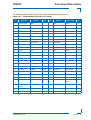
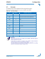
1
CP6012
the Intel® Core™ 2 Duo Processor with
the Intel® E7520 Chipset
Doc. ID: 33274, Rev. 3.0
August 23, 2007
User Guide
PRELIMINARY
6U CompactPCI Processor Board based on
the Intel® Core™ Duo Processor and
Preface
CP6012
Revision History
CP6012: 6U CompactPCI Processor Board based on the Intel®
Publication Title: Core™ Duo Processor and the Intel® Core™ 2 Duo Processor
with the Intel® E7520 Chipset
Doc. ID: 33274
PRELIMINARY
Rev.
Brief Description of Changes
Date of Issue
1.0
Initial issue
25-Aug-2006
2.0
General update
21-Dec-2006
3.0
General update, deletion of appendix C, AMIBIOS8
23-Aug-2007
Imprint
Kontron Modular Computers GmbH may be contacted via the following:
MAILING ADDRESS
TELEPHONE AND E-MAIL
Kontron Modular Computers GmbH
Sudetenstraße 7
D - 87600 Kaufbeuren Germany
+49 (0) 800-SALESKONTRON
[email protected]
For further information about other Kontron products, please visit our Internet web site:
www.kontron.com.
Disclaimer
Copyright © 2007 Kontron AG. All rights reserved. All data is for information purposes only and
not guaranteed for legal purposes. Information has been carefully checked and is believed to
be accurate; however, no responsibility is assumed for inaccuracies. Kontron and the Kontron
logo and all other trademarks or registered trademarks are the property of their respective owners and are recognized. Specifications are subject to change without notice.
Page ii
ID 33274, Rev. 3.0
CP6012
Preface
Revision History .........................................................................................................ii
Imprint ........................................................................................................................ii
Disclaimer ..................................................................................................................ii
Table of Contents ...................................................................................................... iii
List of Tables .............................................................................................................ix
List of Figures ......................................................................................................... xiii
Proprietary Note .......................................................................................................xv
Trademarks ..............................................................................................................xv
Environmental Protection Statement ........................................................................xv
Explanation of Symbols .......................................................................................... xvi
For Your Safety ...................................................................................................... xvii
High Voltage Safety Instructions ........................................................................ xvii
Special Handling and Unpacking Instructions ................................................... xvii
General Instructions on Usage ............................................................................. xviii
Two Year Warranty .................................................................................................. xix
1.
Introduction ............................................................................. 1 - 3
1.1 Board Overview ....................................................................................... 1 - 3
1.2 Board-Specific Information ...................................................................... 1 - 4
1.3 System Expansion Capabilities ............................................................... 1 - 5
1.3.1
PMC Modules ................................................................................. 1 - 5
1.3.2
XMC Modules ................................................................................. 1 - 5
1.3.3
CTM80-3 Rear I/O Module ............................................................. 1 - 5
1.3.4
CP6012-EXT-SATA Module ............................................................ 1 - 5
1.4 System Relevant Information .................................................................. 1 - 6
1.5 Board Diagrams ...................................................................................... 1 - 7
1.5.1
Functional Block Diagram ............................................................... 1 - 7
1.5.2
Front Panel ..................................................................................... 1 - 8
1.5.3
Board Layout .................................................................................. 1 - 9
1.6 Technical Specification .......................................................................... 1 - 11
1.7 Kontron Software Support ..................................................................... 1 - 17
1.8 Standards .............................................................................................. 1 - 17
1.9 Related Publications ............................................................................. 1 - 18
ID 33274, Rev. 3.0
Page iii
PRELIMINARY
Table of Contents
Preface
2.
CP6012
Functional Description ............................................................ 2 - 3
2.1 CPU, Memory and Chipset ......................................................................2 - 3
2.1.1
CPU .................................................................................................2 - 3
2.1.2
Memory ...........................................................................................2 - 5
2.1.3
Intel® E7520 Chipset Overview ......................................................2 - 6
2.1.3.1
Memory Controller Hub E7520 ...............................................2 - 6
2.1.3.2
I/O Controller Hub 6300ESB ...................................................2 - 6
PRELIMINARY
2.2 Peripherals ...............................................................................................2 - 7
2.2.1
Timer ...............................................................................................2 - 7
2.2.2
Watchdog Timer ..............................................................................2 - 7
2.2.3
Battery .............................................................................................2 - 7
2.2.4
Reset ...............................................................................................2 - 8
2.2.5
SMBus Devices ...............................................................................2 - 8
2.2.6
Thermal Management/System Monitoring ......................................2 - 9
2.2.7
Serial EEPROM ..............................................................................2 - 9
2.2.8
FLASH Memory ...............................................................................2 - 9
2.2.8.1
BIOS FLASH (Firmware Hub) .................................................2 - 9
2.2.8.2
CompactFlash .........................................................................2 - 9
2.3 Board Interfaces ....................................................................................2 - 10
2.3.1
Front Panel LEDs ..........................................................................2 - 10
2.3.1.1
IPMI LEDs .............................................................................2 - 10
2.3.1.2
Watchdog and Overtemperature LEDs .................................2 - 10
2.3.1.3
Front-I and Front-II General Purpose LEDs .......................... 2 - 11
2.3.1.4
Hot Swap LED ...................................................................... 2 - 11
2.3.2
USB Interfaces ..............................................................................2 - 12
2.3.3
Graphics Controller .......................................................................2 - 12
2.3.3.1
Video Resolution ...................................................................2 - 13
2.3.3.2
CRT Interface and Connector J10 ........................................2 - 13
2.3.4
COM Ports .....................................................................................2 - 14
2.3.5
Floppy Drive Interface ...................................................................2 - 14
2.3.6
Gigabit Ethernet ............................................................................2 - 15
2.3.7
EIDE Interfaces .............................................................................2 - 16
2.3.7.1
2.3.8
Page iv
CompactFlash Socket ...........................................................2 - 16
Extension Connector J12 ..............................................................2 - 18
ID 33274, Rev. 3.0
CP6012
2.3.9
Preface
Keyboard/Mouse Interface ............................................................ 2 - 18
2.3.10 Serial ATA Interface ...................................................................... 2 - 19
2.3.11 Serial ATA Connector J22 ............................................................. 2 - 19
2.3.12 2.5" SATA HDD Extension Connectors J23 (Optional) ................. 2 - 20
2.3.13 PMC Interface ............................................................................... 2 - 21
2.3.13.1
PMC Connectors J25, J26, J27 and J28 Pinouts
............ 2 - 22
2.3.14 XMC Interface ............................................................................... 2 - 24
2.3.15.1
System Master Configuration ............................................... 2 - 25
2.3.15.2
Peripheral Master Configuration (Passive Mode) ................ 2 - 25
2.3.15.3
Packet Switching Backplane (PICMG 2.16) ......................... 2 - 25
2.3.15.4
Hot Swap Support ................................................................ 2 - 25
2.3.15.5
Power Ramping .................................................................... 2 - 25
2.3.15.6
Precharge ............................................................................. 2 - 25
2.3.15.7
Handle Switch ...................................................................... 2 - 26
2.3.15.8
ENUM# Interrupt .................................................................. 2 - 26
2.3.15.9
Hot Swap LED ...................................................................... 2 - 26
2.3.16 CompactPCI Bus Connector ......................................................... 2 - 27
2.3.16.1
CompactPCI Connector Keying ........................................... 2 - 27
2.3.16.2
CompactPCI Connectors J1 and J2 Pinouts ........................ 2 - 28
2.3.16.3
CompactPCI Rear I/O Connectors J3-J5 and Pinouts ......... 2 - 32
2.3.16.4
Rear I/O Configuration ......................................................... 2 - 36
2.4 Intelligent Platform Management Interface ............................................ 2 - 37
2.4.1
Technical Background of IPMI ...................................................... 2 - 37
2.4.2
IPMI Glossary ........................................................................................2 - 38
2.4.3
IPMI Implementation on the CP6012 ............................................ 2 - 39
2.4.3.1
2.4.4
3.
Sensors Implemented on the CP6012 ................................. 2 - 40
Data Repositories ......................................................................... 2 - 41
Installation ............................................................................... 3 - 3
3.1 Safety Requirements ............................................................................... 3 - 3
3.2 CP6012 Initial Installation Procedures .................................................... 3 - 4
3.3 Standard Removal Procedures ............................................................... 3 - 5
ID 33274, Rev. 3.0
Page v
PRELIMINARY
2.3.15 CompactPCI Interface .................................................................. 2 - 25
Preface
CP6012
3.4 Hot Swap Procedures ..............................................................................3 - 5
3.4.1
System Master Hot Swap ................................................................3 - 5
3.4.2
Peripheral Hot Swap Procedure ......................................................3 - 6
3.5 Installation of CP6012 Peripheral Devices ..............................................3 - 7
3.5.1
CompactFlash Installation ...............................................................3 - 7
3.5.2
USB Device Installation ...................................................................3 - 7
3.5.3
Rear I/O Device Installation .............................................................3 - 8
3.5.4
Battery Replacement .......................................................................3 - 8
3.5.5
Hard Disk Installation ......................................................................3 - 8
PRELIMINARY
3.6 Software Installation ................................................................................3 - 9
4.
Configuration ........................................................................... 4 - 3
4.1 Jumper Description ..................................................................................4 - 3
4.1.1
Clearing BIOS CMOS Setup ...........................................................4 - 3
4.1.2
Shorting Chassis GND (Shield) to Logic GND ................................4 - 3
4.1.3
BIOS Firmware Hub Flash Configuration ........................................4 - 4
4.1.4
M66EN Configuration ......................................................................4 - 4
4.2 Interrupts ..................................................................................................4 - 5
4.3 Onboard PCI Interrupt Routing ................................................................4 - 6
4.4 Memory Map ............................................................................................4 - 7
4.4.1
Memory Map for the 1st Megabyte .................................................4 - 7
4.4.2
I/O Address Map .............................................................................4 - 8
4.5 CP6012-Specific Registers ......................................................................4 - 9
4.5.1
BIOS Boot Order Control Register ..................................................4 - 9
4.5.2
Watchdog Timer Control Register .................................................4 - 10
4.5.3
Geographic Addressing Register ..................................................4 - 12
4.5.4
Hardware and Logic Revision Index Register ...............................4 - 12
4.5.5
CPCI Reset Status Register ..........................................................4 - 13
4.5.6
I/O Status Register ........................................................................4 - 14
4.5.7
I/O Configuration Register .............................................................4 - 15
4.5.8
Board ID Register ..........................................................................4 - 16
4.5.9
Board Interrupt Configuration Register .........................................4 - 17
4.5.10 Hot Swap Status Register .............................................................4 - 18
Page vi
ID 33274, Rev. 3.0
CP6012
Preface
4.5.11 Board-Specific LED Control Register ........................................... 4 - 19
4.5.12 Delay Timer Control/Status Register ............................................ 4 - 20
4.6 BMC-Specific Registers ........................................................................ 4 - 21
4.6.1
BMC Configuration Register ......................................................... 4 - 21
4.6.1.1
4.6.2
5.
BMC Interrupt Configuration Register .................................. 4 - 22
IPMI Keyboard Control Style Interface ......................................... 4 - 23
Power Considerations ............................................................ 5 - 3
5.1.1
CP6012 Baseboard ........................................................................ 5 - 3
5.1.2
Backplane ....................................................................................... 5 - 4
5.1.3
Power Supply Units ........................................................................ 5 - 4
5.1.3.1
Start-Up Requirement ............................................................ 5 - 4
5.1.3.2
Power-Up Sequence .............................................................. 5 - 5
5.1.3.3
Tolerance ................................................................................ 5 - 5
5.1.3.4
Regulation .............................................................................. 5 - 6
5.1.3.5
Rise Time Diagram ................................................................ 5 - 6
5.2 Power Consumption ................................................................................ 5 - 7
5.2.1
Power Consumption of the CP6012 Accessories ........................... 5 - 9
5.2.2
Power Consumption of the Dual Gigabit Ethernet Controller ......... 5 - 9
5.3 Start-Up Currents of the CP6012 .......................................................... 5 - 10
5.4 Power Available for PMC Devices ......................................................... 5 - 10
6.
Thermal Considerations ......................................................... 6 - 3
6.1 Board Internal Thermal Regulation ......................................................... 6 - 3
6.1.1
CPU Internal Thermal Supervision ................................................. 6 - 3
6.1.2
CPU Emergency Thermal Supervision (Thermtrip) ........................ 6 - 4
6.2 Thermal Management Recommendations .............................................. 6 - 4
6.3 External Thermal Regulation ................................................................... 6 - 5
6.3.1
Heat Sink ........................................................................................ 6 - 5
6.3.2
Forced Airflow ................................................................................. 6 - 5
6.3.3
Thermal Characteristic Graphs ....................................................... 6 - 6
6.3.4
Peripherals ...................................................................................... 6 - 9
ID 33274, Rev. 3.0
Page vii
PRELIMINARY
5.1 System Power ......................................................................................... 5 - 3
Preface
A.
CP6012
CTM80-3 RIO Module .............................................................. A - 3
A.1 Introduction ............................................................................................. A - 3
B.
CP6012-EXT-SATA .................................................................. B - 3
B.1 Overview ................................................................................................. B - 3
B.2 Technical Specifications ......................................................................... B - 3
B.3 CP6012-EXT-SATA Functional Block Diagram ....................................... B - 3
B.4 CP6012-EXT-SATA Module Layout ........................................................ B - 4
PRELIMINARY
B.4.1
CP6012-EXT-SATA Module Layout ................................................ B - 4
B.5 Module Interfaces ................................................................................... B - 5
B.5.1
Board-to-Board Connectors J1 and J3 ........................................... B - 5
B.5.2
SATA Connector J2 ........................................................................ B - 6
Page viii
ID 33274, Rev. 3.0
CP6012
Preface
1-1
System Relevant Information .................................................................... 1 - 6
1-2
CP6012 Main Specifications .................................................................... 1 - 11
1-3
Standards ................................................................................................ 1 - 17
1-4
Additional Standards for Boards Ordered with Ruggedized Service ....... 1 - 18
1-5
Related Publications ................................................................................ 1 - 18
2-1
Processors Supported on the CP6012 ...................................................... 2 - 4
2-2
Maximum Power Dissipation of Processors (CPU only) ............................ 2 - 4
2-3
CPU Frequency in the Various SpeedStep® Modes ................................. 2 - 4
2-4
Memory Options Utilizing SODIMM Sockets ............................................. 2 - 5
2-5
SMBus Device Addresses ......................................................................... 2 - 8
2-6
EEPROM Address Map ............................................................................. 2 - 9
2-7
IPMI LEDs Function ................................................................................. 2 - 10
2-9
Front-I and Front-II LEDs Function .......................................................... 2 - 11
2-8
Watchdog and Overtemperature LEDs Function ..................................... 2 - 11
2-10 USB Connectors J7 and J8 Pinout .......................................................... 2 - 12
2-11 Partial List of Display Modes Supported .................................................. 2 - 13
2-12 D-Sub CRT Connector J10 Pinout ........................................................... 2 - 13
2-13 Serial Port Con. J9 (COM1) Pinout ......................................................... 2 - 14
2-14 Pinouts of J6A/B Based on the Implementation ...................................... 2 - 15
2-15 CompactFlash Connector J17 Pinout ...................................................... 2 - 17
2-16 Keyboard Connector J21 Pinout .............................................................. 2 - 18
2-17 SATA Connector J22 Pinout .................................................................... 2 - 19
2-18 SATA Extension Connector J23 Pinout ................................................... 2 - 20
2-19 Onboard PCI Configuration ..................................................................... 2 - 21
2-20 PMC Connectors J26 and J28 Pinouts .................................................... 2 - 22
2-21 PMC Connectors J25 and J27 Pinouts .................................................... 2 - 23
2-22 XMC Connector J15 Pinout ..................................................................... 2 - 24
2-23 Coding Key Colors on J1 ......................................................................... 2 - 27
2-24 CompactPCI Bus Connector J1 System Slot Pinout ............................... 2 - 28
2-25 CompactPCI Bus Connector J1 Peripheral Slot Pinout ........................... 2 - 29
2-26 64-bit CompactPCI Bus Connector J2 System Slot Pinout ..................... 2 - 30
2-27 64-bit CompactPCI Bus Connector J2 Peripheral Slot Pinout ................. 2 - 31
ID 33274, Rev. 3.0
Page ix
PRELIMINARY
List of Tables
Preface
CP6012
2-28 CompactPCI Rear I/O Connector J3 Pinout ............................................. 2 - 32
2-29 CompactPCI Rear I/O Connector J3 Signals ........................................... 2 - 33
2-30 CompactPCI Rear I/O Connector J4 Pinout ............................................. 2 - 34
2-32 CompactPCI Rear I/O Connector J5 Signals ........................................... 2 - 35
2-31 CompactPCI Rear I/O Connector J5 Pinout ............................................. 2 - 35
2-33 Processor and Chipset Supervision ......................................................... 2 - 40
2-34 CompactPCI Sensors ............................................................................... 2 - 40
2-35 Onboard Power Supply Supervision ........................................................ 2 - 40
2-36 Reset Control ........................................................................................... 2 - 40
PRELIMINARY
2-37 Onboard Voltage Sensors ........................................................................ 2 - 41
2-38 Temperature Sensors ............................................................................... 2 - 41
2-39 Fan Sense Sensors .................................................................................. 2 - 41
3-1
ATA Channel Routing ................................................................................. 3 - 9
4-1
Clearing BIOS CMOS Setup ...................................................................... 4 - 3
4-2
BIOS Firmware Hub Flash Configuration ................................................... 4 - 4
4-3
M66EN Configuration ................................................................................. 4 - 4
4-4
Interrupt Setting .......................................................................................... 4 - 5
4-5
PCI Interrupt Routing ................................................................................. 4 - 6
4-6
Memory Map for the 1st Megabyte ............................................................ 4 - 7
4-7
I/O Address Map ........................................................................................ 4 - 8
4-8
BIOS Boot Order Control Register ............................................................. 4 - 9
4-9
Watchdog Timer Control Register ............................................................ 4 - 11
4-10 Geographic Addressing Register ............................................................. 4 - 12
4-11 Hardware and Logic Revision Index Register .......................................... 4 - 12
4-12 CPCI Reset Status Register ..................................................................... 4 - 13
4-13 I/O Status Register ................................................................................... 4 - 14
4-14 I/O Configuration Register ........................................................................ 4 - 15
4-15 Board ID Register ..................................................................................... 4 - 16
4-16 Board Interrupt Configuration Register .................................................... 4 - 17
4-17 Hot Swap Status Register ........................................................................ 4 - 18
4-18 Board-Specific LED Control Register ....................................................... 4 - 19
4-19 Delay Timer Control/Status Register ....................................................... 4 - 20
4-20 BMC Configuration Register .................................................................... 4 - 21
4-21 COM Port Routing for the Firmware Update ............................................ 4 - 22
Page x
ID 33274, Rev. 3.0
CP6012
Preface
5-1
Maximum Input Power Voltage Limits ........................................................ 5 - 3
5-2
DC Operational Input Voltage Ranges ...................................................... 5 - 3
5-3
Input Voltage Characteristics ..................................................................... 5 - 5
5-4
Power Consumption: CP6012 with DOS ................................................... 5 - 8
5-5
Power Consumption: CP6012 wit Linux/Win. XP in IDLE Mode ............... 5 - 8
5-6
Power Consumption: CP6012’s TDP at 75% ............................................ 5 - 8
5-7
Power Consumption: CP6012’s TDP at 100% .......................................... 5 - 8
5-8
Power Consumption of CP6012 Accessories ............................................ 5 - 9
5-9
Intel® 82571EB Dual Gigabit Ethernet Controller Power Supply .............. 5 - 9
5-10 Start-Up Currents of the CP6012 ............................................................. 5 - 10
5-11 Maximum Output Power Limits ................................................................ 5 - 10
B-1
CP6012-EXT-SATA Main Specifications .................................................... B - 3
B-2
Board-to-Board Connector J1 Pinout ........................................................ B - 5
B-3
SATA Connector J2 Pinout ........................................................................ B - 6
ID 33274, Rev. 3.0
Page xi
PRELIMINARY
4-22 BMC Interrupt Configuration Register ..................................................... 4 - 22
PRELIMINARY
Preface
CP6012
This page has been intentionally left blank.
Page xii
ID 33274, Rev. 3.0
CP6012
Preface
1-1
CP6012 Functional Block Diagram .......................................................... 1 - 7
1-2
CP6012 Front Panel ................................................................................ 1 - 8
1-3
CP6012 Board Layout (Front View) ......................................................... 1 - 9
1-4
CP6012 Board Layout (Reverse View) .................................................. 1 - 10
2-1
USB Connectors J7 and J8 .................................................................... 2 - 12
2-2
D-Sub CRT Con. J10 ............................................................................. 2 - 13
2-3
Serial Port Con. J9 (COM1) ................................................................... 2 - 14
2-4
Dual Gigabit Ethernet Connector J6A/B ................................................ 2 - 15
2-5
Extension Con. J12 ................................................................................ 2 - 18
2-6
Keyboard Connector J21 ....................................................................... 2 - 18
2-7
SATA Connector J22 .............................................................................. 2 - 19
2-8
SATA Ext. Con. J23 ............................................................................... 2 - 20
2-9
Connecting an Onboard 2.5" SATA HDD to CP6012-EXT-SATA ........... 2 - 20
2-10
PMC Connectors J25, J26, J27 and J28 ............................................... 2 - 21
2-11
CPCI Connectors J1-J5 ......................................................................... 2 - 27
6-1
Start-Up Ramp of the CP3-SVE180 AC Power Supply ............................ 5 - 6
6-1
Operational Limits for the CP6012 with Core™ Duo 1.66 GHz ............... 6 - 7
6-2
Operational Limits for the CP6012 with Core™ Duo 2.0 GHz ................. 6 - 7
6-3
Operational Limits for the CP6012 with Core™ 2 Duo 1.5 GHz .............. 6 - 8
6-4
Operational Limits for the CP6012 with Core™ 2 Duo 2.16 GHz ............ 6 - 8
A-1
CTM80-3 RIO Module with SCSI Configuration ....................................... A - 4
A-2
CTM80-3 RIO Module with PATA or SATA Configuration ........................ A - 5
B-1
CP6012-EXT-SATA Functional Block Diagram ........................................ B - 3
B-2
CP6012-EXT-SATA Module Layout ......................................................... B - 4
B-3
SATA Connector J2 .................................................................................. B - 6
ID 33274, Rev. 3.0
Page xiii
PRELIMINARY
List of Figures
PRELIMINARY
Preface
CP6012
This page has been intentionally left blank.
Page xiv
ID 33274, Rev. 3.0
CP6012
Preface
Proprietary Note
This document contains information proprietary to Kontron. It may not be copied or transmitted
by any means, disclosed to others, or stored in any retrieval system or media without the prior
written consent of Kontron or one of its authorized agents.
The information contained in this document is, to the best of our knowledge, entirely correct.
However, Kontron cannot accept liability for any inaccuracies or the consequences thereof, or
for any liability arising from the use or application of any circuit, product, or example shown in
this document.
Trademarks
Kontron, the PEP logo and, if occurring in this manual, “CXM” are trademarks owned by Kontron, Kaufbeuren (Germany). In addition, this document may include names, company logos
and trademarks, which are registered trademarks and, therefore, proprietary to their respective
owners.
Environmental Protection Statement
This product has been manufactured to satisfy environmental protection requirements where
possible. Many of the components used (structural parts, printed circuit boards, connectors,
batteries, etc.) are capable of being recycled.
Final disposition of this product after its service life must be accomplished in accordance with
applicable country, state, or local laws or regulations.
ID 33274, Rev. 3.0
Page xv
PRELIMINARY
Kontron reserves the right to change, modify, or improve this document or the product
described herein, as seen fit by Kontron without further notice.
Preface
CP6012
Explanation of Symbols
Caution, Electric Shock!
This symbol and title warn of hazards due to electrical shocks (> 60V)
when touching products or parts of them. Failure to observe the precautions indicated and/or prescribed by the law may endanger your
life/health and/or result in damage to your material.
Please refer also to the section “High Voltage Safety Instructions” on
the following page.
Warning, ESD Sensitive Device!
PRELIMINARY
This symbol and title inform that electronic boards and their components are sensitive to static electricity. Therefore, care must be taken
during all handling operations and inspections of this product, in
order to ensure product integrity at all times.
Please read also the section “Special Handling and Unpacking
Instructions” on the following page.
Warning!
This symbol and title emphasize points which, if not fully understood
and taken into consideration by the reader, may endanger your health
and/or result in damage to your material.
Note ...
This symbol and title emphasize aspects the reader should read
through carefully for his or her own advantage.
Page xvi
ID 33274, Rev. 3.0
CP6012
Preface
For Your Safety
Your new Kontron product was developed and tested carefully to provide all features necessary
to ensure its compliance with electrical safety requirements. It was also designed for a long
fault-free life. However, the life expectancy of your product can be drastically reduced by
improper treatment during unpacking and installation. Therefore, in the interest of your own
safety and of the correct operation of your new Kontron product, you are requested to conform
with the following guidelines.
High Voltage Safety Instructions
Warning!
Caution, Electric Shock!
Before installing a not hot-swappable Kontron product into a system
always ensure that your mains power is switched off. This applies
also to the installation of piggybacks.
Serious electrical shock hazards can exist during all installation,
repair and maintenance operations with this product. Therefore,
always unplug the power cable and any other cables which provide
external voltages before performing work.
Special Handling and Unpacking Instructions
ESD Sensitive Device!
Electronic boards and their components are sensitive to static electricity. Therefore, care must be taken during all handling operations
and inspections of this product, in order to ensure product integrity at
all times.
Do not handle this product out of its protective enclosure while it is not used for operational
purposes unless it is otherwise protected.
Whenever possible, unpack or pack this product only at EOS/ESD safe work stations. Where
a safe work station is not guaranteed, it is important for the user to be electrically discharged
before touching the product with his/her hands or tools. This is most easily done by touching a
metal part of your system housing.
It is particularly important to observe standard anti-static precautions when changing piggybacks, ROM devices, jumper settings etc. If the product contains batteries for RTC or memory
backup, ensure that the board is not placed on conductive surfaces, including anti-static plastics or sponges. They can cause short circuits and damage the batteries or conductive circuits
on the board.
ID 33274, Rev. 3.0
Page xvii
PRELIMINARY
All operations on this device must be carried out by sufficiently skilled
personnel only.
Preface
CP6012
General Instructions on Usage
In order to maintain Kontron’s product warranty, this product must not be altered or modified in
any way. Changes or modifications to the device, which are not explicitly approved by Kontron
and described in this manual or received from Kontron’s Technical Support as a special
handling instruction, will void your warranty.
This device should only be installed in or connected to systems that fulfill all necessary
technical and specific environmental requirements. This applies also to the operational
temperature range of the specific board version, which must not be exceeded. If batteries are
present, their temperature restrictions must be taken into account.
PRELIMINARY
In performing all necessary installation and application operations, please follow only the
instructions supplied by the present manual.
Keep all the original packaging material for future storage or warranty shipments. If it is
necessary to store or ship the board, please re-pack it as nearly as possible in the manner in
which it was delivered.
Special care is necessary when handling or unpacking the product. Please consult the special
handling and unpacking instruction on the previous page of this manual.
Page xviii
ID 33274, Rev. 3.0
CP6012
Preface
Two Year Warranty
Kontron grants the original purchaser of Kontron’s products a TWO YEAR LIMITED HARDWARE
as described in the following. However, no other warranties that may be granted or
implied by anyone on behalf of Kontron are valid unless the consumer has the express written
consent of Kontron.
Kontron warrants their own products, excluding software, to be free from manufacturing and
material defects for a period of 24 consecutive months from the date of purchase. This warranty
is not transferable nor extendible to cover any other users or long-term storage of the product.
It does not cover products which have been modified, altered or repaired by any other party
than Kontron or their authorized agents. Furthermore, any product which has been, or is suspected of being damaged as a result of negligence, improper use, incorrect handling, servicing
or maintenance, or which has been damaged as a result of excessive current/voltage or temperature, or which has had its serial number(s), any other markings or parts thereof altered, defaced or removed will also be excluded from this warranty.
If the customer’s eligibility for warranty has not been voided, in the event of any claim, he may
return the product at the earliest possible convenience to the original place of purchase, together with a copy of the original document of purchase, a full description of the application the
product is used on and a description of the defect. Pack the product in such a way as to ensure
safe transportation (see our safety instructions).
Kontron provides for repair or replacement of any part, assembly or sub-assembly at their own
discretion, or to refund the original cost of purchase, if appropriate. In the event of repair, refunding or replacement of any part, the ownership of the removed or replaced parts reverts to
Kontron, and the remaining part of the original guarantee, or any new guarantee to cover the
repaired or replaced items, will be transferred to cover the new or repaired items. Any extensions to the original guarantee are considered gestures of goodwill, and will be defined in the
“Repair Report” issued by Kontron with the repaired or replaced item.
Kontron will not accept liability for any further claims resulting directly or indirectly from any
warranty claim, other than the above specified repair, replacement or refunding. In particular,
all claims for damage to any system or process in which the product was employed, or any loss
incurred as a result of the product not functioning at any given time, are excluded. The extent
of Kontron liability to the customer shall not exceed the original purchase price of the item for
which the claim exists.
Kontron issues no warranty or representation, either explicit or implicit, with respect to its
products’ reliability, fitness, quality, marketability or ability to fulfil any particular application or
purpose. As a result, the products are sold “as is,” and the responsibility to ensure their
suitability for any given task remains that of the purchaser. In no event will Kontron be liable for
direct, indirect or consequential damages resulting from the use of our hardware or software
products, or documentation, even if Kontron were advised of the possibility of such claims prior
to the purchase of the product or during any period since the date of its purchase.
Please remember that no Kontron employee, dealer or agent is authorized to make any
modification or addition to the above specified terms, either verbally or in any other form, written
or electronically transmitted, without the company’s consent.
ID 33274, Rev. 3.0
Page xix
PRELIMINARY
WARRANTY
PRELIMINARY
Preface
CP6012
This page has been intentionally left blank.
Page xx
ID 33274, Rev. 3.0
Introduction
Chapter
1
Introduction
ID 33274, Rev. 3.0
Page 1 - 1
PRELIMINARY
CP6012
PRELIMINARY
Introduction
CP6012
This page has been intentionally left blank.
Page 1 - 2
ID 33274, Rev. 3.0
CP6012
1.
Introduction
1.1
Board Overview
Introduction
The CP6012 is a highly integrated 6U CompactPCI system controller board based on the Intel®
Core™ Duo and the Intel® Core™ 2 Duo microprocessors combined with the highperformance Intel® E7520 and Intel® 6300ESB server-class chipsets.
The Intel® Core™ Duo and the Intel® Core™ 2 Duo are low-power dual-core processors supporting Intel’s Virtualization Technology (VT). The Intel® Core™ Duo consists of two cores and
up to 2 MB L2 cache shared by both cores. The Intel® Core™ 2 Duo consists of two cores, up
to 4 MB L2 cache shared by both cores, Intel® Extended Memory 64 Technology (Intel®
EM64T), and enhanced address range for up to 64 GB memory. The Intel® Core™ Duo and
the Intel® Core™ 2 Duo processors deliver optimized power-efficient computing and outstanding dual-core performance with low power consumption.
The board includes two SODIMM sockets to provide up to 4 GB dual-channel, registered,
second-generation Double Data Rate (DDR2) memory with Error Checking and Correcting
(ECC) running at 400 MHz (PC3200) for rugged environments. Two Intel® 82571EB Dual
Gigabit Ethernet controllers each of them utilizing a x4 lane PCI Express interconnection to the
E7520 chipset ensures maximum data throughput between processor and memory.
The CP6012 offers more features and expandability than other CompactPCI boards in its class.
The board comes with four Gigabit Ethernet ports, up to four USB 2.0 ports, two Ultra ATA/100
interfaces with one of them connected to a CompactFlash type II socket, two onboard Serial
ATA interfaces, one PMC interface with 64-bit/66 MHz on the PCI bus, one XMC interface
utilizing a x8 lane PCI Express interconnection, rear I/O with several interfaces, and an ATI
ES1000 2D Graphics accelerator with 64 MB of DDR2 memory for enhanced graphics
performance with a VGA CRT-display interface. Several onboard connectors provide flexible
expandability.
The board supports a configurable 64-bit/66 MHz, hot swap CompactPCI interface. In the
System Master slot the interface is enabled, and if installed in a peripheral slot, the CP6012 is
isolated from the CompactPCI bus.
A further feature of the CP6012 is its support of the PICMG CompactPCI Packet Switching
Backplane Specification 2.16. When installed in a backplane which supports packet switching,
the CP6012 can communicate via two Gigabit Ethernet interfaces with other peripherals.
Designed for stability and packaged in a rugged format, the board fits into all applications
situated in industrial environments, including I/O intensive applications where only one slot is
available for the CPU, making it a perfect core technology for long-life applications.
Components with high temperature tolerance have been selected from embedded technology
programs, and therefore offer long-term availability.
The board is offered with Linux, Microsoft® Windows® XP, Windows® XP Embedded and
Microsoft® Windows® Server 2003 operating systems. Please contact Kontron for further
information concerning the operation of the CP6012 with other operating systems.
ID 33274, Rev. 3.0
Page 1 - 3
PRELIMINARY
The board is capable of supporting the Intel® Core™ Duo and the Intel® Core™ 2 Duo
processor versions in 65 nm technology with 64 kB L1 and up to 4 MB L2 cache in a 479
µFCBGA package with frequencies ranging from 1.06 GHz up to 2.16 GHz providing up to 667
MHz front side bus speed.
Introduction
1.2
CP6012
Board-Specific Information
The CP6012 is a CompactPCI single-board computer based on the Intel® Core™ Duo and the
Intel® Core™ 2 Duo processors and specifically designed for use in highly integrated platforms
with solid mechanical interfacing for a wide range of industrial environment applications.
PRELIMINARY
Some of the CP6012's outstanding features are:
• Supports all Intel® Core™ Duo and Intel® Core™ 2 Duo microprocessors with up to 667
MHz FSB
• 479-pin µFCBGA package
• 64 kB L1 and up to 4 MB L2 cache on-die, running at CPU speed
• Intel® E7520 and Intel® 6300ESB chipset
• Up to 4GB registered DDR2 SDRAM registered memory with ECC
• 2D high performance VGA controller, 32-bit/33 MHz PCI
• Analog display support up to 1600 x 1200 pixels at 16-bit and 75 Hz
• 64-bit / 66 MHz CompactPCI interface in accordance with the CompactPCI Spec. Rev 3.0
• PMC interface with rear I/O support and bezel cutout on front panel and PCI functionality,
64-bit/66 MHz PCI, 3.3V only
• XMC interface utilizing a x8 lane PCI Express
• Four Gigabit Ethernet interfaces utilizing a x4 lane PCI Express per Gigabit Ethernet controller
• Two Gigabit Ethernet interfaces on the front panel
• Two Gigabit Ethernet interfaces on rear I/O (PICMG 2.16)
• Two EIDE Ultra ATA/100 interfaces
• Two Serial ATA interfaces
• Optional socket for Serial ATA 2.5" hard disk (depending on heat sink)
• Onboard CompactFlash type II socket (True IDE)
• Up to four USB ports
• Two USB 2.0 ports on the front panel
• Two USB 2.0 ports on rear I/O
• AMI BIOS
• Two 1 MB onboard FWH for redundant BIOS
• Floppy disk interface on rear I/O
• Watchdog Timer
• Real-time clock
• Two COM ports (RS-232):
• One COM port either on the front panel or on the rear I/O
• One COM port on the rear I/O
• I/O extension connector (LPC)
• 4HP, 6U CompactPCI
• Jumperless board configuration
• Passive heat sink solution for external airflow
• Hot swap capability: as system controller or as peripheral device
• Supports PICMG Packet Switching Backplane Specification 2.16
• Several rear I/O configurations
• Rear I/O on J3 and J5; optionally on J4
• IPMI compliant Baseboard Management Controller
Page 1 - 4
ID 33274, Rev. 3.0
CP6012
1.3
System Expansion Capabilities
1.3.1
PMC Modules
Introduction
The CP6012 has one PCI, 64-bit/66 MHz, 3.3V, rear I/O capable, PMC mezzanine interface.
This interface supports a wide range of available PMC modules with PCI interface including all
of Kontron’s PMC modules and provides an easy and flexible way to configure the CP6012 for
various application requirements.
For information on the PMC interface, refer to chapter 2.3.13, "PMC Interface".
1.3.2
XMC Modules
For information on the XMC interface, refer to chapter 2.3.14, "XMC Interface".
1.3.3
CTM80-3 Rear I/O Module
The CTM80-3 rear I/O module has been designed for use with the CP6012 6U CompactPCI
board from Kontron. This module provides comprehensive rear I/O functionality and may also
be configured for use in other applications.
For further information concerning the CTM80-3 module, please refer to Appendix A.
1.3.4
CP6012-EXT-SATA Module
The CP6012-EXT-SATA module has been designed for use with the CP6012 6U CompactPCI
board from Kontron and enables the user to connect an onboard 2.5" Serial ATA hard disk to
the CP6012.
For further information concerning the CP6012-EXT-SATA module, please refer to Appendix B.
ID 33274, Rev. 3.0
Page 1 - 5
PRELIMINARY
The CP6012 has one XMC mezzanine interface for support of x1, x2, x4 and x8 PCI Express
XMC modules providing an easy and flexible way to configure the CP6012 for various application requirements.
Introduction
1.4
CP6012
System Relevant Information
The following system relevant information is general in nature but should still be considered
when developing applications using the CP6012.
Table 1-1: System Relevant Information
SUBJECT
System Slot / System Master
Functionality
INFORMATION
The CP6012 is designed for use as a System Master board whereby it can
support up to 7 peripheral boards with up to 64-bit / 66 MHz.
PRELIMINARY
It may, however, be operated in a peripheral slot in which case it does not
support the CompactPCI bus interface.
Peripheral Slot Functionality
When installed in a peripheral slot, the CP6012 is electrically isolated from
the CompactPCI bus. It receives power from the backplane and supports rear
I/O and, if the system supports it, packet switching (in this case up to two
channels of Gigabit Ethernet).
Hot Swap Compatibility
When operated as a System Master, the CP6012 supports individual clocks
for each slot and ENUM signal handling is in compliance with the PICMG 2.1
Hot Swap Specification.
When operated in a peripheral slot the CP6012 supports basic hot swap.
Operating Systems
The CP6012 can be operated under the following operating systems:
• Microsoft® Windows® XP with Service Pack 1 or higher
• Microsoft® Windows® XP Embedded
• Microsoft® Windows® Server 2003
• Linux
Please contact Kontron for further information concerning the operation of
the CP6012 with other operating systems.
Page 1 - 6
ID 33274, Rev. 3.0
CP6012
1.5
Introduction
Board Diagrams
The following diagrams provide additional information concerning board functionality and
component layout.
1.5.1
Functional Block Diagram
Figure 1-1:
CP6012 Functional Block Diagram
Gigabit
Gigabit
Ethernet
Ethernet
82571EB
82571EB
J3CPCI
CPCI
J3
VGA
COM 1/2
Key/Mouse
USB 3/4
PICMG 2.16
Ethernet
Ethernet
DDR2400
400MHz
MHz
DDR2
withECC
ECC
with
Uptoto22GB
GB
Up
Gigabit
Gigabit
Ethernet
Ethernet
82571EB
82571EB
x4 PCI Express
E7520
E7520
x4 PCI Express
Ethernet
Ethernet
RJ45
RJ45
x8 PCI Express
PCItotoPCI
PCI
PCI
Bridge
Bridge
HUB 266 MB/s
667 MHz
Power
Power
Supply
Supply
Temp.
Temp.
RJ45
RJ45
Intel®®
Intel
Core™
™
Core
6300ESB
6300ESB
Duo/ /22Duo
Duo
Duo
CompactFlash
CompactFlash
type II
type II
LPC
IPMI
IPMI
BIOS
BIOS
2xFWH
2xFWH
1MB
1MB
COM1
COM1
9-pin
9-pin
Keyboard
Keyboard
ID 33274, Rev. 3.0
Super
Super
I/O
I/O
Floppy
Floppy
I/O
I/O
Ext.
Ext.
2.5“HDD
HDD
2.5“
PMC
PMC
64-bit/66 MHz
64-bit/66 MHz
oror
XMC x8 lane
PCI 64-bit XMC x8 lane
PCI 32-bit
USB 2.0
USB 2.0
2x4-pin
2x4-pin
VGA
VGA
J1/J2CPCI
CPCI
J1/J2
HotSwap
Swap
Hot
CPCI PCI
64-bit/66 MHz
IPMB
Hot Swap
J5CPCI
CPCI
J5
SATA 1/2
Floppy
EIDE Secon.
J4CPCI
CPCI
J4
PMC Rear I/O
CRTVGA
VGA
CRT
Front Panel Connectors
Onboard Connectors
Page 1 - 7
PRELIMINARY
DDR2400
400MHz
MHz
DDR2
withECC
ECC
with
Up to 2 GB
Up to 2 GB
Introduction
1.5.2
CP6012
Front Panel
Figure 1-2: CP6012 Front Panel
Legend:
IPMI LEDs
IPMI (green): Indicate the software status of the IPMI controller
General Purpose LEDs
WD (green): Watchdog Status
PRELIMINARY
TH (green): Overtemperature Status
HS (blue): Hot Swap Control
Front-I: General Purpose/POST code or board-specific
Front-II: General Purpose/POST code or board-specific
Integral Ethernet LEDs
ACT (green):
SPEED (green/orange):
Ethernet Link/Activity
Ethernet Speed
SPEED ON (orange):
1000 Mbit
SPEED ON (green):
100 Mbit
SPEED OFF:
10 Mbit
Note ...
If the TH LED and the WD LED are flashing during boot-up, a failure is indicated before the
BIOS has started.
For further information, contact Kontron’s Technical Support.
Page 1 - 8
ID 33274, Rev. 3.0
CP6012
1.5.3
Introduction
Board Layout
Figure 1-3:
CP6012 Board Layout (Front View)
22
2
21
1
J12
J21
J19 J20
A1
1
F1
2
2
1
Bank B
J14
J26
J15
J28
J5
A19
63
F19 1
SODIMM Socket
64
63
64
2
1
2
J13
J25
J27
Bank A
J4
63
63
64
64
Magnetics
7
J10
VGA
Controller
E7520
MCH
1
Magnetics
J22
IPMI
LEDs
2
1
12
11
J3
J23
6300ESB
ICH
J9
WD/TH
LEDs
J8
CPU
J2
GP/
POST
CODE
LEDs
J7
J6B
Magnetics
J1
J6A
Magnetics
HS LED
GbE
GbE
J17
CompactFlash Socket
J11
ID 33274, Rev. 3.0
Page 1 - 9
PRELIMINARY
SODIMM Socket
Introduction
Figure 1-4:
CP6012
CP6012 Board Layout (Reverse View)
Super
I/O
BMC
Contr.
Logic
BIOS
PRELIMINARY
BIOS
VGA
Mem.
UARTs
JP4
Bridge
Page 1 - 10
ID 33274, Rev. 3.0
CP6012
1.6
Introduction
Technical Specification
Table 1-2:
CP6012 Main Specifications
CP6012
CPU
SPECIFICATIONS
The CP6012 supports the following microprocessors:
•
•
•
•
Intel® Core™ Duo, T2500 (SV), 2.0 GHz, 667 MHz FSB, 2 MB L2 cache
Intel® Core™ Duo, L2400 (LV), 1.66 GHz, 667 MHz FSB, 2 MB L2 cache
Intel® Core™ 2 Duo, T7400 (SV), 2.16 GHz, 667 MHz FSB, 4 MB L2 cache
Intel® Core™ 2 Duo, L7400 (LV), 1.5 GHz, 667 MHz FSB, 4 MB L2 cache
Memory
Main Memory:
• Up to 4 GB dual-channel, registered DDR2 memory with Error Checking
and Correcting (ECC) running at 400 MHz (PC3200)
PRELIMINARY
Processor and Memory
All microprocessors are provided in a 479 µFCBGA packaging.
Cache structure:
• 64 kB L1 on-die full speed processor cache
• 32 kB for instruction cache
• 32 kB for data cache
• Up to 4 MB L2 on-die full speed processor cache
FLASH Memory:
• Two 1 MB FLASH for redundant BIOS
Memory Extension:
• CompactFlash socket type II (true IDE mode)
Serial EEPROM:
• 24LC64 (64 kbit)
ID 33274, Rev. 3.0
Page 1 - 11
Introduction
Table 1-2:
CP6012
CP6012 Main Specifications (Continued)
CP6012
Intel® E7520
SPECIFICATIONS
Intel® E7520 Memory Controller Hub:
• Support for a single Intel® Core™ Duo or Intel® Core™ 2 Duo microprocessor
• 64-bit AGTL/AGTL+ based System Bus interface up to 667 MHz
• System Memory interface with optimized support for dual-channel, registered DDR2 SDRAM memory at 400 MHz with ECC
Chipset
PRELIMINARY
• Two x4 PCI Express ports for Gigabit Ethernet interface
• One x8 PCI Express port for XMC interface
• RASUM (Reliability, Availability, Serviceability, Usability, and Manageability) features:
• Memory error detection and reporting of 1- and 2-bit errors including
correction of 1-bit failures
• Integrated Memory Scrub Engine, which logs any uncorrectable
memory errors
• Support for automatic read retry on uncorrectable errors
Intel® 6300ESB
Intel® 6300ESB I/O Controller Hub:
•
•
•
•
•
•
•
•
•
•
•
•
Page 1 - 12
Dual channel SATA 150 interface
Integrated IDE controller Ultra ATA/100/66/33
USB host interface with up to four USB 1.1 or USB 2.0 ports
Firmware Hub interface support
Low pin count interface
PCI Rev. 2.2 compliant with support for 64-bit/66 MHz PCI operations
PCI Rev. 2.2 compliant with support for 32-bit/33 MHz PCI operations
Power management logic support
Enhanced DMA controller, interrupt controller, and timer functions
System Management Bus (SMBus) compatible with most I²C™ devices
Hub interface for the E7520 MCH
RTC controller
ID 33274, Rev. 3.0
CP6012
Table 1-2:
Introduction
CP6012 Main Specifications (Continued)
CP6012
CompactPCI
SPECIFICATIONS
Compliant with CompactPCI Specification PICMG ® 2.0 R 3.0
• System Master operation
• 64-bit / 66 MHz master interface
• 3.3V or 5V compliant
When the CP6012 is operated in a peripheral slot, the CompactPCI bus is electrically isolated (passive mode).
Rear I/O
The following interfaces are routed to the rear I/O connector J3, J4 and J5:
•
•
•
•
•
•
•
•
Interfaces
Hot Swap Compatible
is necessary
2 x USB 2.0
CRT VGA
PS/2 (Mouse / Keyboard)
2 x Gigabit Ethernet (compliant with PICMG 2.16, R 1.0)
Secondary EIDE (ATA 100)
2 x SATA 150
PMC rear I/O
Floppy disk interface
The CP6012 supports System Master hot swap functionality and application
dependent hot swap functionality when used in a peripheral slot.
When used as a System Master the CP6012 supports individual clocks for
each slot and ENUM signal handling is in compliance with the PICMG 2.1 Hot
Swap Specification.
VGA
ATI ES1000 2D Graphics accelerator for enhanced graphics performance.
• Supports resolutions of up to 1600 x 1200 by 16-bit color resolution
•
•
Gigabit Ethernet
at a 75 Hz refresh rate or up to 1280 x 1024 by 32-bit color resolution
at an 75 Hz refresh rate.
The graphics controller provides 64 MB video memory.
One CRT controller capable of supporting two identical simultaneous display paths.
Up to four 10 Base-T/100 Base-TX/1000 Base-T Gigabit Ethernet interfaces based on two Intel® 82571EB Ethernet PCI Express bus controllers.
Two channels on rear I/O
Two RJ45 connectors on the front panel
Automatic mode recognition (Auto-Negotiation)
Automatic cabling configuration recognition (Auto-MDI/X)
Cabling requirement: Category 5, UTP, four-pair cabling
•
•
•
•
USB
Four USB ports supporting UHCI and EHCI:
• Two USB 2.0 connectors on the front panel
• Two USB 2.0 on the rear I/O interface
ID 33274, Rev. 3.0
Page 1 - 13
PRELIMINARY
• COM1 and COM2 (RS-232 signaling); no buffer on the rear I/O module
Introduction
Table 1-2:
CP6012
CP6012 Main Specifications (Continued)
CP6012
SPECIFICATIONS
Serial
Two 16C550-compatible UARTs on the rear I/O interface (RS-232 signaling),
one thereof can be routed to the front panel
PMC
CMC / PMC P1386 / Draft 2.4a compliant mezzanine interface
• Jn1, Jn2, Jn3 and Jn4 PCI mezzanine connectors for standard PMC
•
•
•
•
XMC interface
• Onboard XMC connector J15
• Up to x8 lanes PCI Express
• Rear I/O supported through the PMC connector Jn4 (J27) to the CompactPCI connector J4
Keyboard and Mouse
Keyboard and mouse are supported
• USB Support on 4HP
• PS/2 (keyboard and mouse) with rear I/O module (e.g. CTM80-3)
• Onboard keyboard pinrow connector for debug purposes requiring an
adapter in order to be connected to a regular keyboard
Interfaces
PRELIMINARY
XMC
modules
64-bit / 66 MHz PCI interface
Only 3.3V compatible
Rear I/O supported through the CompactPCI connector J4
Supported voltages: 3.3 V, 5 V, +12 V, and -12 V
Mass Storage
EIDE Ultra ATA/100/66/33:
• Two onboard Ultra ATA/100 interfaces, one on CompactFlash and one
on Rear I/O
• Up to three devices (one CompactFlash and up to two hard disks or CDROMs)
Onboard 2.5" hard disk:
• Onboard 2.5" hard disk is supported on a 22-pin Serial ATA interface
(only for low-voltage CPU)
• For the Serial ATA interface, the CP6012-EXT-SATA module is used
CompactFlash:
• CompactFlash type II socket (true IDE mode and DMA support)
• Supports type I and II CompactFlash cards and Microdrive™
SATA: Integrated Serial ATA Host Controllers
• Provide independent DMA operation on 2 channels:
• One SATA channel switchable to rear I/O via BIOS (for standard
HDDs)
• One SATA channel routed either to the SATA connector J22 or to
rear I/O (for 2.5" HDDs)
• Data transfer rates up to 150 MB/s
Floppy Disk (only with rear I/O module):
• Supports 5.25" or 3.5" floppy drives
• 1.44 or 2.88 MB, 3.5" floppy disks
I/O Extension Interface
Page 1 - 14
I/O extension interface:
• LPC devices
ID 33274, Rev. 3.0
CP6012
CP6012 Main Specifications (Continued)
CP6012
SPECIFICATIONS
•
•
•
•
•
Onboard Connectors
• CompactFlash socket for type I, II and MicroDrive devices (primary
Sockets
Front Panel Connectors
•
•
•
•
•
•
LEDs
VGA: 15-pin, D-Sub connector
USB: two 4-pin connectors
Ethernet: two RJ-45 connectors
COM: 9-pin, D-Sub connector
PMC/XMC front panel
EIDE interface)
I/O extension connector
PMC connectors J25 - J28 (Jn1 - Jn4)
XMC connector, J15
Two SATA connectors
• one 7-pin, standard SATA connector
• one optional 12-pin, SATA extension connector
CompactPCI Connector J1 and J2 (J3 - J5 optional)
Two 200-pin SODIMM sockets
System status:
• TH (green): Overtemperature Status
• WD (green): Watchdog Status
• IPMI:
Control information
Gigabit Ethernet status:
• ACT (green):
network activity
• SPEED (green / orange): network speed
HW Monitoring
General Purpose LEDs:
• I (green):
• II (green):
General Purpose/POST code or board-specific
General Purpose/POST code or board-specific
Watchdog
Software configurable Watchdog generates IRQ, NMI, or hardware reset.
Thermal Management
CPU overtemperature protection is provided by:
• Internal processor temperature control unit
• CPU shut down via hardware monitor
System Monitor
In SCH3112 integrated hardware monitor for supervision of:
• Several system power voltages
• Two fan speed inputs
• Board temperature
IPMI
Baseboard Management Controller (BMC) that supports two keyboard
controller-style interfaces (KCS) compliant with:
• IPMI specification 1.5, revision 1.5
• PICMG 2.9 specification
IPMI supports two IPMB busses via the J1 and J2 connectors.
ID 33274, Rev. 3.0
Page 1 - 15
PRELIMINARY
Table 1-2:
Introduction
Introduction
Table 1-2:
CP6012
CP6012 Main Specifications (Continued)
CP6012
AMI BIOS with 1 MB Flash memory with the following features:
• QuickBoot
• QuietBoot
• BootBlock
• LAN boot capability for diskless systems (standard PXE)
• Boot from USB floppy disk drive
• BIOS boot support for USB keyboards
• Plug and Play capability
• BIOS parameters are saved in the EEPROM
• Board serial number is saved within the EEPROM
• PC Health Monitoring
Operating Systems
Operating systems supported:
Software
Software BIOS
•
•
•
•
Microsoft® Windows® XP
Microsoft® Windows® XP Embedded
Microsoft® Windows® Server 2003
Linux
Mechanical
6U, 4HP, CompactPCI compliant form factor
Power Consumption
See Chapter 5 for details
Temperature Ranges
Operational:
0°C to +60°C
Storage: -55°C to +85°C
-40°C to +65°C
Standard
Without hard disk and without battery
With hard disk and without battery
Note ...
General
PRELIMINARY
SPECIFICATIONS
When a battery is installed, refer to the operational specifications of the battery as this determines the storage temperature of the CP6012
(See "Battery" below).
Climatic Humidity
93% RH at 40 °C, non-condensing (acc. to IEC 60068-2-78)
Dimensions
233.35 mm x 160 mm
Board Weight
691 g (4HP variants with wide heat sink and without mezzanine boards)
Battery
3.0V lithium battery for RTC with battery socket. Recommended types:
• VARTA CR2025
• PANASONIC BR2020
Temperature ranges:
Operational: -20°C to +70°C
Storage: -55°C to +70°C
Page 1 - 16
typical (refer to the battery manufacturer’s
specifications for exact range)
typical (no discharge)
ID 33274, Rev. 3.0
CP6012
1.7
Introduction
Kontron Software Support
Kontron is one of the few CompactPCI and VME manufacturers providing inhouse support for
most of the industry-proven real-time operating systems that are currently available. Due to its
close relationship with the software manufacturers, Kontron is able to produce and support
BSPs and drivers for the latest operating system revisions thereby taking advantage of the
changes in technology.
Finally, customers possessing a maintenance agreement with Kontron can be guaranteed
hotline software support and are supplied with regular software updates. A dedicated web site
is also provided for online updates and release downloads.
Standards
This product complies with the requirements of the following standards:
Table 1-3:
Standards
TYPE
CE
ASPECT
STANDARD
Emission
EN55022
EN61000-6-3
Immission
EN55024
EN61000-6-2
Electrical Safety
EN60950-1
Mechanical
Mechanical Dimensions
IEEE 1101.10
Environmental
Climatic Humidity
IEC60068-2-78
WEEE
Directive 2002/96/EC
Waste electrical and electronic equipment
RoHS
Directive 2002/95/EC
Restriction of the use of certain hazardous substances in electrical and electronic equipment
ID 33274, Rev. 3.0
Page 1 - 17
PRELIMINARY
1.8
Introduction
CP6012
In addition, boards ordered with the ruggedized service comply with the following standards as
well.
Table 1-4:
Additional Standards for Boards Ordered with Ruggedized Service
TYPE
ASPECT
PRELIMINARY
Environmental
1.9
STANDARD
REMARKS
Vibration
(Sinusoidal)
IEC60068-2-6
Ruggedized version test parameters:
• 10-300 (Hz) frequency range
• 2 (g) acceleration
• 1 (oct/min) sweep rate
• 10 cycles/axis
• 3 axis
Random Vibration
(Broadband)
IEC60068-2-64
Ruggedized version test parameters:
• 20-500Hz, 0.05 (g²/Hz) PSD
• 500-2000Hz, 0.005 (g²/Hz) PSD
• 3.5 (g RMS) acceleration
• 30 (min) test time/axis
• 3 axis
Permanent Shock
IEC60068-2-29
Ruggedized version test parameters:
• 15 (g) acceleration
• 11 (ms) pulse duration
• 500 bumps per direction
• 6 directions
• 1 (s) recovery time
Single Shock
IEC60068-2-27
Ruggedized version test parameters:
• 30 (g) acceleration
• 9 (ms) pulse duration
• 3 shocks per direction
• 6 directions
• 5 (s) recovery time
Related Publications
The following publications contain information relating to this product.
Table 1-5:
Related Publications
PRODUCT
CompactPCI Systems and
Boards
PUBLICATION
CompactPCI Specification 2.0, Rev. 3.0
CompactPCI Packet Switching Backplane Specification PICMG 2.16 Rev. 2.0
CompactPCI System Management Specification PICMG 2.9 Rev. 1.0
CompactPCI Hot Swap Specification PICMG 2.1 Rev. 2.0
Hot Swap Specification PICMG 2.1
Kontron CompactPCI Backplane Manual, ID 24229
CompactFlash Cards
CF+ and CompactFlash Specification Revision 2.1
PMC Modules
Draft Standard for a Common Mezzanine Card Family: CMC, P1386/Draft 2.4a,
21-Mar-01
Page 1 - 18
ID 33274, Rev. 3.0
Functional Description
Chapter
21
Functional Description
ID 33274, Rev. 3.0
Page 2 - 1
PRELIMINARY
CP6012
PRELIMINARY
Functional Description
CP6012
This page has been intentionally left blank.
Page 2 - 2
ID 33274, Rev. 3.0
CP6012
2.
Functional Description
2.1
CPU, Memory and Chipset
2.1.1
CPU
Functional Description
The CP6012 supports the latest Intel® Core™ Duo and Intel® Core™ 2 Duo processor family
up to speeds of 2.16 GHz with up to 667 MHz FSB, such as:
Intel® Core™ Duo, L2400 (LV), 1.66 GHz, 667 MHz FSB, 2 MB L2 cache
Intel® Core™ Duo, T2500 (SV), 2.0 GHz, 667 MHz FSB, 2 MB L2 cache
Intel® Core™ 2 Duo, L7400 (LV), 1.5 GHz, 667 MHz FSB, 4 MB L2 cache
Intel® Core™ 2 Duo, T7400 (SV), 2.16 GHz, 667 MHz FSB, 4 MB L2 cache
The Intel® Core™ Duo consists of two cores and up to 2 MB L2 cache shared by both cores.
The Intel® Core™ 2 Duo consists of two cores, up to 4 MB L2 cache shared by both cores,
Intel® Extended Memory 64 Technology (Intel® EM64T), and enhanced address range for up
to 64 GB memory. The Intel® Core™ Duo and the Intel® Core™ 2 Duo processors deliver optimized power-efficient computing and outstanding dual-core performance with low power consumption.
The Intel® Core™ Duo and the Intel® Core™ 2 Duo support the latest Intel’s Virtualization
Technology (VT), which allows a platform to run multiple operating systems and applications in
independent partitions, such as performing system upgrades and maintenance without interrupting the system or the application, keeping software loads and virus attacks separate, combining multiple servers in one system, etc. With processor and I/O enhancements to Intel’s
various platforms, Intel Virtualization Technology improves the performance and robustness of
today’s software-only virtual machine solutions.
Furthermore, the Intel® Core™ Duo and the Intel® Core™ 2 Duo processors also support the
Intel® SpeedStep® technology which enables real-time dynamic switching of the voltage and
frequency between several modes. This is achieved by switching the bus ratios, core operating
voltage, and core processor speeds without resetting the system. The frequency for the processor may also be selected in the BIOS or via the operating system.
The following list sets out some of the key features of the Intel® Core™ Duo and the Intel®
Core™ 2 Duo processors:
•
•
•
•
•
•
•
•
•
•
Two mobile execution cores in one single processor
Support of Intel’s Virtualization Technology (Vanderpool)
Support of Intel Architecture with Dynamic Execution
Outstanding dual-core performance with low power consumption
On-die, primary 32 kB instruction cache and 32 kB write-back data cache
On-die, L1 and L2 cache with Advanced Transfer Cache Architecture
Advanced Branch Prediction and Data Prefetch Logic
Streaming SIMD Extensions 3 (SSE3)
Up to 667 MHz, Source-Synchronous Front Side Bus (FSB)
Advanced Power Management features including Enhanced Intel® SpeedStep® technology
• Intel® Extended Memory 64 Technology for 64-bit computing (only with Intel® Core™ 2
Duo)
• Enhanced address range for up to 64 GB memory (only with Intel® Core™ 2 Duo)
ID 33274, Rev. 3.0
Page 2 - 3
PRELIMINARY
•
•
•
•
Functional Description
CP6012
The following tables indicate the Intel® Core™ Duo and the Intel® Core™ 2 Duo processors
supported on the CP6012, their maximum power dissipation and their frequency in the various
SpeedStep® modes.
Table 2-1:
SPEED
Core™ Duo
1.66 GHz (LV)
2 MB L2 Cache
Core™ Duo
2.0 GHz
2 MB L2 Cache
Core™ 2 Duo
1.5 GHz (LV)
4 MB L2 Cache
Core™ 2 Duo
2.16 GHz
4 MB L2 Cache
PACKAGE
µFCBGA
µFCBGA
µFCBGA
µFCBGA
L2 CACHE
2 MB
2 MB
4 MB
4 MB
FSB
667 MHz
667 MHz
667 MHz
667 MHz
Table 2-2:
PRELIMINARY
Processors Supported on the CP6012
Maximum Power Dissipation of Processors (CPU only)
Core™ Duo
1.66 GHz (LV)
2 MB L2 Cache
Core™ Duo
2.0 GHz
2 MB L2 Cache
Core™ 2 Duo
1.5 GHz (LV)
4 MB L2 Cache
Core™ 2 Duo
2.16 GHz
4 MB L2 Cache
Maximum Power HFM1)
15 W
31 W
17 W
34 W
Maximum Power LFM 2)
13.1 W
13.1 W
15.1 W
20 W
FREQUENCY MODE
1)
HFM High Frequency Mode (maximum frequency of the CPU)
2)LFM
Low Frequency Mode (frequency is 1.0 GHz)
Note ...
Only the 1.5 GHz and 1.66 GHz low-voltage processors are able to operate with
onboard 2.5 HDD because of the lower power dissipation.
Table 2-3:
CPU Frequency in the Various SpeedStep® Modes
FREQUENCY
Core™ Duo
1.66 GHz (LV)
2 MB L2 Cache
Core™ Duo
2.0 GHz
2 MB L2 Cache
Core™ 2 Duo
1.5 GHz (LV)
4 MB L2 Cache
Core™ 2 Duo
2.16 GHz
4 MB L2 Cache
2.16 GHz
--
--
--
x
2.0 GHz
--
x
--
--
1.66 GHz
x
x
--
x
1.5 GHz
--
--
x
--
1.33 GHz
x
x
--
x
1.0 GHz
x
x
x
x
Page 2 - 4
ID 33274, Rev. 3.0
CP6012
2.1.2
Functional Description
Memory
The CP6012 supports a dual-channel (72-bit), registered Double Data Rate (DDR2) memory
with Error Checking and Correcting (ECC) running at 400 MHz (PC3200). It provides two 200pin SODIMM sockets for the DDR2 SODIMM modules that support up to 4 GB system memory.
The available memory module configuration can be either 1 GB, 2 GB, or 4 GB.
There are several Reliability, Availability, Serviceability, Usability, and Manageability (RASUM)
features available for the memory interface:
• Memory error detection and reporting of 1 and 2 bit errors and correction of 1 bit failures
• Integrated Memory Scrub Engine, the scrub engine logs any uncorrectable memory error
• Support for automatic read retry on uncorrectable errors
Table 2-4:
Memory Options Utilizing SODIMM Sockets
BANK A
BANK B
TOTAL
512 MB
--
512 MB
512 MB
512 MB
1 GB
1 GB
1 GB
2 GB
2 GB
2 GB
4 GB
Warning!
Even though the registered DDR2 SODIMM modules from Kontron have the
same keying as conventional DDR SODIMM modules, their pinout is different.
For this reason, only registered DDR2 SODIMM modules from Kontron are permitted to be used on the CP6012. Use of any other type of DDR2 SODIMM
modules on the CP6012 will void your warranty and result in damage to the
board or the system.
ID 33274, Rev. 3.0
Page 2 - 5
PRELIMINARY
Only qualified DDR2 SODIMM modules from Kontron are authorized by Kontron for use with
the CP6012.
Functional Description
2.1.3
CP6012
Intel® E7520 Chipset Overview
The Intel® E7520 chipset consists of the following devices:
• Intel® E7520 Memory Controller Hub (MCH)
• Intel® 6300ESB I/O Controller Hub (ICH)
The MCH provides the processor interface for the Intel® Core™ Duo and the Intel® Core™ 2
Duo microprocessors, the memory bus, the PCI Express bus, and the hub link interface to ICH.
The ICH is a centralized controller for the boards’ I/O peripherals such as the USB 2.0 and the
IDE port. The Firmware Hub Flash provides the non-volatile storage for the BIOS.
PRELIMINARY
2.1.3.1
Memory Controller Hub E7520
The E7520 Memory Controller Hub (MCH) is a highly integrated hub that provides the CPU interface, a dual-channel DDR2 SDRAM system memory interface (optimized for DDR400/
PC3200), two x4 and one x8 PCI Express interfaces, and a high-speed hub link interface to the
6300ESB I/O Controller Hub.
2.1.3.2
I/O Controller Hub 6300ESB
The 6300ESB is a highly integrated multifunctional I/O Controller Hub that provides the interface to two PCI Buses, and integrates many of the functions needed in today's PC platforms,
such as Ultra DMA 100/66/33 controller, SATA 150, USB host controller supporting USB 2.0,
LPC interface and FWH Flash BIOS interface controller. The 6300ESB communicates with the
host controller over a dedicated hub interface.
The I/O Controller Hub feature set comprises:
•
•
•
•
•
•
•
•
•
•
•
•
Dual channel SATA 150 interface
Integrated IDE controller Ultra ATA/100/66/33
USB host interface with up to four USB 1.1 or USB 2.0 ports
Firmware Hub interface support
Low pin count interface
PCI Rev. 2.2 compliant with support for 32-bit/33 MHz PCI operations
PCI Rev. 2.2 compliant with support for 64-bit/66 MHz PCI operations
Power management logic support
Enhanced DMA controller, interrupt controller, and timer functions
System Management Bus (SMBus) compatible with most I²C™ devices
Hub interface for the E7520 MCH
RTC controller
Page 2 - 6
ID 33274, Rev. 3.0
CP6012
2.2
Functional Description
Peripherals
The following standard peripherals are available on the CP6012 board:
2.2.1
Timer
• Real-time clock
The 6300ESB contains a MC146818A compatible real-time clock with 256 bytes of battery-backed RAM.
The real-time clock performs timekeeping functions and includes 256 bytes of general
purpose battery-backed CMOS RAM. Features include an alarm function, programmable
periodic interrupt and a 100-year calendar. All battery-backed CMOS RAM data remains
stored in an additional EEPROM. This prevents data loss.
• In addition to the three 8254-style counters, the 6300ESB includes three individual multimedia event timers that may be used by the operating system. They are implemented
as a single counter each with its own comparator and value register.
• Hardware delay timer for short reliable delay times
2.2.2
Watchdog Timer
A Watchdog Timer is provided, which forces either an IRQ5, NMI, or Reset condition
(configurable in the Watchdog Register). The Watchdog Timer can be programmed in 12 steps
ranging from 125 msec up to 256 seconds. If the Watchdog Timer is enabled, it cannot be
stopped.
2.2.3
Battery
The CP6012 is provided with a 3.0 V “coin cell” lithium battery for the RTC.
To replace the battery, proceed as follows:
•
•
•
•
Turn off power
Remove the battery
Place the new battery in the socket.
Make sure that you insert the battery the right way round. The plus pole must be on the top!
The lithium battery must be replaced with an identical battery or a battery type recommended
by the manufacturer. Suitable batteries include the VARTA CR2025 and PANASONIC BR2020.
Note ...
The user must be aware that the battery’s operational temperature range is
less than that of the CP6012’s storage temperature range.
For exact range information, refer to the battery manufacturer’s specifications.
ID 33274, Rev. 3.0
Page 2 - 7
PRELIMINARY
The CP6012 is equipped with the following timers:
Functional Description
CP6012
Note ...
Care must be taken to ensure that the battery is correctly replaced.
The battery should be replaced only with an identical or equivalent type
recommended by the manufacturer.
Dispose of used batteries according to the manufacturer’s instructions.
The typical life expectancy of a 170 mAh battery (VARTA CR2025) is 5 - 6
years with an average on-time of 8 hours per working day at an operating
temperature of 30°C. However, this typical value varies considerably because
the life expectancy is dependent on the operating temperature and the
standby time (shutdown time) of the system in which it operates.
PRELIMINARY
To ensure that the lifetime of the battery has not been exceeded, it is recommended to exchange the battery after 4 - 5 years.
2.2.4
Reset
The CP6012 is automatically reset by a precision voltage monitoring circuit that detects a drop
in voltage below the acceptable operating limit of 4.25 V for the 5 V line and below 2.8 V for the
3.3 V line, or in the event of a power failure of the DC/DC converter. Other reset sources include
the Watchdog Timer and the push-button switch on the front panel. The CP6012 responds to
any of these sources by initializing local peripherals.
A reset will be generated under the following conditions:
•
•
•
•
•
•
+5 V supply falls below 4.25 V (typ.)
+3.3 V supply falls below 2.8 V (typ.)
Power failure of all onboard DC/DC converters
Push-button "RESET" pressed
Watchdog overflow
CompactPCI backplane PRST input
2.2.5
SMBus Devices
The CP6012 provides a System Management Bus (SMBus) for access to several system
monitoring and configuration functions. The SMBus consists of a two-wire I²C bus interface.
The following table describes the function and address of every onboard SMBus device.
Table 2-5:
SMBus Device Addresses
DEVICE
SMB ADDRESS
EEPROM 24LC64
1010101xb
Clock (core)
1101001xb
Clock (PCI Express)
1101110xb
SPD (channel A)
1010011xb
SPD (channel B)
1010010xb
Page 2 - 8
ID 33274, Rev. 3.0
CP6012
2.2.6
Functional Description
Thermal Management/System Monitoring
The SCH3112 can be used to monitor several critical hardware parameters of the system,
including power supply voltages, fan speeds and temperatures, all of which are very important
for the proper operation and stability of a high-end computer system. The SCH3112 provides
an LPC interface.
The voltages +12 V, +5 V, +3.3 V, +1.8 V, and Vcore are supervised. Two fan tachometer
outputs can be measured using the SCH3112's FAN inputs.
The temperature sensors on the SCH3112 monitor the temperature around the DDR2 memory
module and the internal temperature of the SCH3112.
2.2.7
Serial EEPROM
Table 2-6:
EEPROM Address Map
ADDRESS
FUNCTION
0x000 - 0x0FF
CMOS backup
0x100 - 0x1FF
Production data
0x200 - 0x3FF
OS Boot parameter
0x400 - 0x1FFF
User
2.2.8
FLASH Memory
There are two flash devices available as described below, one for the BIOS and one for the
CompactFlash socket.
2.2.8.1
BIOS FLASH (Firmware Hub)
The CP6012 provides two redundant Firmware Hub Flash chips (2x1MB). The fail-over
mechanism for the BIOS recovery can be controlled via the BMC controller or the jumper. If one
Firmware Hub Flash is corrupted, the BMC can enable the second Firmware Hub Flash and
boot the system again.
For detailed information on BIOS refer to Appendix C.
2.2.8.2
CompactFlash
CompactFlash is a very small removable mass storage device. It provides true IDE functionality
compatible with the 16-bit ATA/ATAPI-4 interface.
For further information on the CompactFlash, refer to section 2.3.7.1, CompactFlash Socket.
ID 33274, Rev. 3.0
Page 2 - 9
PRELIMINARY
This EEPROM is connected to the I²C bus provided by the 6300ESB.
Functional Description
2.3
Board Interfaces
2.3.1
Front Panel LEDs
CP6012
The CP6012 is equipped with two IPMI LEDs, one Watchdog LED, one Overtemperature LED,
eight General Purpose/POST code or board-specific LEDs (four LEDs for Front-I and four
LEDs for Front-II), and one Hot Swap LED. Their functionality is described in the following
chapters.
2.3.1.1
IPMI LEDs
The IPMI LEDs show the software status of the IPMI controller. The following table indicates
the function of the IPMI LEDs.
PRELIMINARY
Table 2-7:
IPMI LEDs Function
Normal status
LEFT LED
RIGHT LED
OFF
SLOW BLINKING
Blinking
speed
Slow
(100 msec ON;
1.4 sec OFF)
Fast
8 x (150 msec ON;
50 msec OFF)
Slow
(250 msec ON;
3 sec OFF)
Fast
8 x (150 msec ON;
50 msec OFF)
Signification
Management Controller
request attention to
SMS/SMM
(this may occur when
there is a message
waiting for the SMS)
Send/Receive data
through the IPMB bus
The Management Controller is running normally; it’s a heart beat
Send/Receive data
through the KCS interface
2.3.1.2
Watchdog and Overtemperature LEDs
The CP6012 provides one LED for Watchdog (WD LED) and one for Overtemperature
(TH LED) status. If the TH LED and the WD LED are flashing during boot-up, a failure is
indicated before the BIOS has started. In this case, check the power supply. If the power supply
appears to be functional and the LEDs are still flashing, contact Kontron’s Technical Support.
Note ...
If only the Overtemperature LED flashes on and off at regular intervals, it indicates that the processor junction temperature has reached a level beyond
which permanent silicon damage may occur. Upon assertion of Thermtrip, the
processor will shut off its internal clocks (thus halting program execution) in an
attempt to reduce the processor junction temperature.
Once activated, Thermtrip remains latched until a cold restart of the CP6012 is
undertaken (all power off and then on again).
Page 2 - 10
ID 33274, Rev. 3.0
CP6012
Watchdog and Overtemperature LEDs Function
FUNCTION DURING
BOOT-UP
LED
DEFAULT FUNCTION AFTER BOOT-UP
WD (green)
A failure is indicated before
the BIOS has started
Watchdog Status
TH (green)
A failure is indicated before
the BIOS has started
Overtemperature Status
2.3.1.3
The TH LED states are:
• Flicker:
If the CPU reaches approximately 100°C
• On:
In case of overtemperature of the CPU, i.e. the CPU
has reached a temperature above 100°C
• Long blink: If the CPU has been shut off, i.e. the CPU has
reached a temperature above 125°C
Front-I and Front-II General Purpose LEDs
There are two sets of General Purpose LEDs available on the front panel of the CP6012 which
are designed to indicate the boot-up POST code and are available to the application as General
Purpose LEDs or board-specific signals.
To POST code is indicated during the boot-up phase. After boot-up, the Front-I and Front-II
LEDs indicate Port 80, General Purpose or board-specific signals, depending on the BIOS settings. The default setting after boot-up is General Purpose.
Together Front-I and Front-II indicate a two-place hexadecimal number. Front-II is the lower
nibble, Front-I is the higher nibble. A ’1’ is indicated by a lit LED. The LSB is 0, the MSB is 7.
The default setting is General Purpose and all LEDs are not lit.
Table 2-9:
Front-I and Front-II LEDs Function
FRONT-I & FRONT-II
GENERAL PURPOSE
LEDs
0
User-defined
1
User-defined
2
User-defined
3
User-defined
4
User-defined
5
User-defined
6
User-defined
7
2.3.1.4
User-defined
PORT 80
LSB
BOARD-SPECIFIC
HDD activity on primary channel
HDD activity on secondary channel
(8-bit data
register,
POST code,
Linux boot code)
HDD activity on SATA channel
Reserved
Reserved
Reserved
Reserved
MSB
Reserved
Hot Swap LED
On the CP6012, a blue HS LED can be switched on or off by software. It may be used, for example, to indicate that the shutdown process is finished and the board is ready for extraction.
It may also be used for general purposes.
ID 33274, Rev. 3.0
Page 2 - 11
PRELIMINARY
Table 2-8:
Functional Description
Functional Description
2.3.2
CP6012
USB Interfaces
The CP6012 supports four USB 2.0 ports (two on the front I/O and two on the rear I/O). On the
two rear I/O ports it is strongly recommended to use a cable below 3 metres in length for
USB 2.0 devices. All four ports are high-speed, full-speed, and low-speed capable. High-speed
USB 2.0 allows data transfers of up to 480 Mb/s - 40 times faster than a full-speed USB
(USB 1.1).
One USB peripheral may be connected to each port. To connect more than four USB devices
an external hub is required.
USB Connectors J7 and J8 Pinout
The CP6012 has two USB interfaces implemented on a 4-pin connector with the following pinout.
PRELIMINARY
Figure 2-1: USB Connectors J7 and J8 Table 2-10: USB Connectors J7 and J8 Pinout
PIN
J7
4 3 2 1
J8
4 3 2 1
SIGNAL
FUNCTION
I/O
1
VCC
VCC
--
2
UV0-
Differential USB-
I/O
3
UV0+
Differential USB+
I/O
4
GND
GND
--
Note ...
The USB power supply to each USB connector is protected with a fuse
(500 mA) and all the signal lines are EMI-filtered.
2.3.3
Graphics Controller
The CP6012 includes a highly integrated graphics controller ATI ES1000 for connecting the
CP6012 to a standard progressive scan monitor. The ATI ES1000 graphics controller provides
a 16-bit wide, 533 MHz fast DDR2 memory interface for connecting it to the video memory. This
interface is only active when running in internal graphics mode.
Integrated 2D Graphics:
•
•
•
•
•
One CRT controller capable of supporting 64 MB DDR2 video memory running at 533 MHz
2D hardware acceleration
Integrated 350 MHz DAC
Resolution up to 1600 x 1200 @ 75 Hz
Optimized for server applications
Page 2 - 12
ID 33274, Rev. 3.0
CP6012
2.3.3.1
Functional Description
Video Resolution
The ES1000 has an integrated 350 MHz RAMDAC that can directly drive a progressive scan
analog monitor up to a resolution of 1600x1200 @ 75 Hz.
Table 2-11: Partial List of Display Modes Supported
COLOR RESOLUTION VERSUS HORIZONTAL FREQUENCY
8-BIT INDEXED
16-BIT
32-BIT
60
75
85
100
60
75
85
100
60
75
85
100
640 x 480
X
X
X
X
X
X
X
X
X
X
X
X
800 x 600
X
X
X
X
X
X
X
X
X
X
X
X
1024 x 7680
X
X
X
X
X
X
X
X
X
X
X
X
1280 x 1024
X
X
X
X
X
X
X
X
X
X
--
--
1600 x 1200
X
X
--
--
X
X
--
--
--
--
--
--
2.3.3.2
CRT Interface and Connector J10
The 15-pin female connector J10 is used to connect a CRT monitor to the CP6012 board.
Figure 2-2: D-Sub CRT Con. J10
Table 2-12: D-Sub CRT Connector J10 Pinout
PIN
10
5
15
11
6
ID 33274, Rev. 3.0
1
SIGNAL
FUNCTION
I/O
1
Red
Red video signal output
O
2
Green
Green video signal output
O
3
Blue
Blue video signal output
O
13
Hsync
Horizontal sync.
TTL Out
14
Vsync
Vertical sync.
TTL Out
12
Sdata
I²C data
I/O
15
Sclk
I²C clock
O
9
VCC
Power +5V, 1.5 A fuse
protection
O
5,6,7,8,10
GND
Ground signal
--
4,11
Free
--
--
Page 2 - 13
PRELIMINARY
DISPLAY MODE
Functional Description
2.3.4
CP6012
COM Ports
The CP6012 provides two COM ports, COM1 and COM2. COM1 is available on the front panel
as a 9-pin, D-Sub, PC-compatible connector, and is routed to rear I/O. COM2 is only available
on the rear I/O module. COM1 and COM2 are fully compatible with the 16550 controller and
include a complete set of handshaking and modem control signals, maskable interrupt generation and data transfer of up to 115.2 kB/s. The two COM ports are configured as RS-232.
The following figure and table provide pinout information for the serial port connector J9.
PRELIMINARY
Figure 2-3: Serial Port Con. J9 (COM1) Table 2-13: Serial Port Con. J9 (COM1) Pinout
6
9
2.3.5
1
5
PIN
RS-232
(STANDARD PC)
1
DCD
2
RXD
3
TXD
4
DTR
5
GND
6
DSR
7
RTS
8
CTS
9
RIN
Floppy Drive Interface
The onboard floppy disk controller supports either 5.25 inch or 3.5 inch (1.44 or 2.88 MB) floppy
disks. The floppy disk port is only available on the CompactPCI rear I/O interface.
Page 2 - 14
ID 33274, Rev. 3.0
CP6012
Gigabit Ethernet
Figure 2-4: Dual Gigabit Ethernet
Connector J6A/B
The CP6012 board provides four 10Base-T/100BaseTX/1000Base-T Ethernet interfaces based on two Intel® 82571EB Gigabit Ethernet controllers, which are
connected to the PCI Express interface. Two Gigabit
Ethernet interfaces are available on the front panel.
Two additional Gigabit Ethernet interfaces are available on the rear I/O in accordance with the PICMG
2.16 specification.
J6B
8
1
J6A
8
The Intel® 82571EB Dual Gigabit Ethernet Control1
ler’s architecture is optimized to deliver high performance with the lowest power consumption. The
controller's architecture includes independent transmit
and receive queues and a PCI Express interface that maximizes the use of bursts for efficient
bus usage.
The Boot from LAN feature is supported.
Note ...
The maximum length of cabling over which the Ethernet transmission can operate effectively depends upon the transceiver in use.
The Ethernet connectors, J6A/B, are realized as RJ45 connectors. The interfaces provide automatic detection and switching between 10Base-T, 100Base-TX and 1000Base-T data transmission (Auto-Negotiation). Auto-wire switching for crossed cables is also supported (AutoMDI/X).
RJ45 Connector J6A/B Pinouts
The J6A/B connector supplies the 10Base-T, 100Base-TX and 1000Base-T interfaces to the
Ethernet controller.
Table 2-14: Pinouts of J6A/B Based on the Implementation
MDI / STANDARD ETHERNET CABLE
10BASE-T
100BASE-TX
1000BASE-T
I/O
SIGNAL
I/O
SIGNAL
I/O
SIGNAL
O
TX+
O
TX+
I/O
BI_DA+
O
TX-
O
TX-
I/O
I
RX+
I
RX+
-
-
-
-
-
I
MDIX / CROSSED ETHERNET CABLE
10BASE-T
100BASE-TX
1000BASE-T
I/O
SIGNAL
I/O
SIGNAL
I/O
SIGNAL
1
I
RX+
I
RX+
I/O
BI_DB+
BI_DA-
2
I
RX-
I
RX-
I/O
BI_DB-
I/O
BI_DB+
3
O
TX+
O
TX+
I/O
BI_DA+
-
I/O
BI_DC+
4
-
-
-
-
I/O
BI_DD+
-
-
I/O
BI_DC-
5
-
-
-
-
I/O
BI_DD-
RX-
I
RX-
I/O
BI_DB-
6
O
TX-
O
TX-
I/O
BI_DA-
-
-
-
-
I/O
BI_DD+
7
-
-
-
-
I/O
BI_DC+
-
-
-
-
I/O
BI_DD-
8
-
-
-
-
I/O
BI_DC-
ID 33274, Rev. 3.0
PIN
Page 2 - 15
PRELIMINARY
2.3.6
Functional Description
Functional Description
CP6012
Ethernet LED Status
ACT (green): This LED monitors network connection and activity. The LED lights up when network packets are sent or received through the RJ45 port. When this LED is not lit it means that
either the computer is not sending or receiving network data or that the cable connection is
faulty.
SPEED (green/orange): This LED lights up to indicate a successful 100Base-TX or
1000BASE-T connection. When green it indicates a 100Base-TX connection and when orange
it indicates a 1000Base-TX connection. When not lit and the ACT-LED is active, the connection
is operating at 10Base-T.
PRELIMINARY
2.3.7
EIDE Interfaces
The CP6012 supports two EIDE interfaces, one for CompactFlash compliant devices and one
on the Rear I/O interface. The EIDE interface on the Rear I/O supports up to two devices (one
master and one slave). All devices can be used in cylinder head sector (CHS) mode with the
BIOS also supporting the logical block addressing (LBA) mode.
2.3.7.1
CompactFlash Socket
To enable flexible flash extension, a CompactFlash (CF) type II socket, J17, is available.
CompactFlash is a very small removable mass storage device. It provides true IDE functionality
compatible with the 16-bit ATA/ATAPI-4 interface.
The CompactFlash socket is connected to the primary EIDE port and can be set to master or
slave.
The board supports DMA and both CF types (type I and type II). CompactFlash is available in
both CF type I and CF type II cards. The Microdrive is a CF type II card.
Note ...
If the CP6012 is ordered with a narrow heat sink, the CompactFlash card can
be replaced. The easiest way to remove the CompactFlash card is to affix a
wide piece of adhesive tape to the top side, then pull it out and afterwards
remove the tape.
If the CP6012 is ordered with a wide heat sink, or a 2.5" HDD is mounted on the
CP6012, the CompactFlash card is not replaceable. If necessary to replace the
CompactFlash card, please contact Kontron for further assistance.
Page 2 - 16
ID 33274, Rev. 3.0
CP6012
Functional Description
The following table provides the pinout for the CompactFlash connector J17.
Table 2-15: CompactFlash Connector J17 Pinout
FUNCTION
SIGNAL
PIN
PIN
SIGNAL
FUNCTION
I/O
--
Ground signal
GND
1
2
D03
Data 3
I/O
I/O
Data 4
D04
3
4
D05
Data 5
I/O
I/O
Data 6
D06
5
6
D07
Data 7
I/O
O
Chip select 0
IDE_CS0
7
8
GND (A10)
--
--
--
--
GND (ATASEL)
9
10
GND (A09)
--
--
--
--
GND (A08)
11
12
GND (A07)
--
--
--
Power 3.3 V
VCC
13
14
GND (A06)
--
--
--
--
GND (A05)
15
16
GND (A04)
--
--
--
--
GND (A03)
17
18
A02
Address 2
O
O
Address 1
A01
19
20
A00
Address 0
O
I/O
Data 0
D00
21
22
D01
Data 1
I/O
I/O
Data 2
D02
23
24
IOCS16
--
O
--
--
NC (CD2)
25
26
NC (CD1)
--
--
I/O
Data 11
D11
27
28
D12
Data 12
I/O
I/O
Data 13
D13
29
30
D14
Data 14
I/O
I/O
Data 15
D15
31
32
IDE_CS1
Chip select 1
O
--
--
NC (VS1)
33
34
IORD
I/O read
O
O
I/O write
IOWR
35
36
WE (VCC)
Write enable
O
I
Interrupt request
INTRQ
37
38
VCC
Power 3.3 V
--
O
Master/Slave
39
40
NC (VS2)
--
--
O
Reset
Reset
41
42
IORDY
I/O ready
I
O
Acknowledge
INPACK
43
44
DACK
Data acknowledge
I
I/O
Drive active slave
present
DASP
45
46
NC (PDIAG)
--
--
I/O
Data 08
D08
47
48
D09
Data 09
I/O
I/O
Data 10
D10
49
50
GND
--
--
ID 33274, Rev. 3.0
CSEL (GND/pull-up)
Page 2 - 17
PRELIMINARY
I/O
Functional Description
2.3.8
CP6012
Extension Connector J12
Figure 2-5: Extension Con. J12
The I/O extension connector provides cost-effective
and flexible configuration options. To provide flexible
configuration of additional low speed PC devices,
such as Super I/O, IPMI or CAN controller, the LPC
port is connected to the I/O extension connector. The
I/O extension interface contains all the signals necessary to connect up to two LPC devices.
2.3.9
1
21
2
22
Keyboard/Mouse Interface
PRELIMINARY
The onboard keyboard controller is 8042 software compatible.
The keyboard and mouse port is routed to the CompactPCI rear I/O interface. There is no front
I/O connector available. To connect a keyboard, a separate onboard connector is available.
The mouse port is only available on the CompactPCI rear I/O interface.
The CP6012 has a 5-pin male pinrow connector, J21, for the keyboard interface.
Figure 2-6: Keyboard Connector J21
Table 2-16: Keyboard Connector J21 Pinout
PIN
5
Page 2 - 18
1
SIGNAL
FUNCTION
I/O
1
KDATA
Keyboard data
I/O
2
--
--
--
3
GND
Ground
--
4
VCC
VCC 5V
--
5
KCLK
Keyboard clock
O
ID 33274, Rev. 3.0
CP6012
2.3.10
Functional Description
Serial ATA Interface
The CP6012 supports the new Serial ATA technology through the SATA interface. The SATA
specification allows for thinner, more flexible cables with lower pin count (only 7 pins, instead
of 40 pins as on standard EIDE). The current Serial ATA interface allows up to 150 MB/s data
transfer rate, which is faster than the standard Parallel ATA with 100 MB/s (Ultra ATA/100). Both
ports are available on the CompactPCI rear I/O interface. A standard SATA HDD can be
connected to the CP6012 either via the SATA connector, J22, or using the CP6012-EXT-SATA
module connected to the optional SATA extension connector, J23.
2.3.11
Serial ATA Connector J22
Figure 2-7: SATA Connector J22 Table 2-17: SATA Connector J22 Pinout
PIN
7
1
SIGNAL
FUNCTION
I/O
1
GND
Ground signal
--
2
SATA_TX1+
Differential Transmit +
O
3
SATA_TX1-
Differential Transmit -
O
4
GND
Ground signal
--
5
SATA_RX1-
Differential Receive -
I
6
SATA_RX1+
Differential Receive +
I
7
GND
Ground signal
--
Note ...
If the onboard SATA interface, J22, will be used, due to the big SATA connector
and the stiffly cable, the CP6012 will have a thickness of 8HP.
ID 33274, Rev. 3.0
Page 2 - 19
PRELIMINARY
The CP6012 is equipped with a SATA connector, J22, which is used to connect standard HDDs
and other SATA devices to the CP6012. This SATA channel can be switched either to the SATA
Connector J22 or to the Rear I/O Connector J5 via the BIOS.
Functional Description
2.3.12
CP6012
2.5" SATA HDD Extension Connectors J23 (Optional)
The CP6012 can be equipped with one optional 12-pin, female SATA extension connector, J23.
This connector is used to connect an onboard 2.5" Serial ATA HDD to the CP6012 through the
CP6012-EXT-SATA module. For further information on the CP6012-EXT-SATA module, refer
to Appendix B.
Figure 2-8: SATA Ext. Con. J23
Table 2-18: SATA Extension Connector J23 Pinout
PIN
PRELIMINARY
2 1
12 11
Figure 2-9:
SIGNAL
FUNCTION
I/O
1
SATA_RX1-
Differential Receive -
I
2
GND
Ground signal
--
3
SATA_RX1+
Differential Receive +
I
4
GND
Ground signal
--
5
GND
Ground signal
--
6
5V
5V power
--
7
SATA_TX1-
Differential Transmit -
O
8
GND
Ground signal
--
9
SATA_TX1+
Differential Transmit +
O
10
GND
Ground signal
--
11
GND
Ground signal
--
12
5V
5V power
--
Connecting an Onboard 2.5" SATA HDD to CP6012-EXT-SATA
2.5” Serial ATA HDD
CP6012-EXT-SATA Module
Page 2 - 20
ID 33274, Rev. 3.0
CP6012
Functional Description
Note ...
There are two heat sink versions available for the CP6012, a wide heat sink for
standard voltage CPUs and a narrow heat sink for low-voltage CPUs.
If the CP6012 is ordered with standard voltage CPU, the mounted wide heat
sink extends partly over the area where the HDD is intended to be installed.
For this reason, a 2.5" HDD can be mounted on the CP6012 only if a narrow
heat sink is used.
2.3.13
PMC Interface
This interface has been designed to comply with the IEEEP1386.1 specification, which defines
a PCI electrical interface for the CMC (Common Mezzanine Card) form factor. The CP6012
provides only 3.3V PMC PCI signaling environment.
Figure 2-10: PMC Connectors J25, J26, J27 and J28
1
2
1
2
J26
J28
Jn1
Jn2
63
64
63
64
1
2
1
2
J25
J27
Jn3
Jn4
63
64
63
64
The PMC interface supports the following configurations:
Table 2-19: Onboard PCI Configuration
SIZE
SPEED
INTERFACE
32-bit
33 MHz
PCI
64-bit
33 MHz
PCI
64-bit
66 MHz
PCI
ID 33274, Rev. 3.0
Page 2 - 21
PRELIMINARY
For flexible and easy configuration one onboard PMC socket is available. The Jn1 and Jn2 connectors provide the signals for the 32-bit PCI Bus. The 64-bit extension for the PMC interface
is supported by the Jn3 connector. User defined I/O signals are supported (Jn4) and are connected to the CompactPCI rear I/O connector J4.
Functional Description
2.3.13.1
CP6012
PMC Connectors J25, J26, J27 and J28 Pinouts
Table 2-20: PMC Connectors J26 and J28 Pinouts
Jn1 (J26)
SIGNAL
PRELIMINARY
TCK (pull-up)
Jn2 (J28)
PIN
PIN
1
2
SIGNAL
-12V
SIGNAL
+12V
PIN
PIN
SIGNAL
1
2
TRST# (pull-down)
Ground
3
4
INTA#
TMS (pull-up)
3
4
TDO (NC)
INTB#
5
6
INTC#
TDI (pull-up)
5
6
Ground
BUSMODE1# (NC)
7
8
+5V
Ground
7
8
PCI-RSV (NC)
INTD#
9
10
PCI-RSV (NC)
PCI-RSV (NC)
9
10
PCI-RSV (NC)
Ground
11
12
3V3-AUX (NC)
BUSMODE2#
(pull-up)
11
12
+3.3V
CLK
13
14
Ground
RST#
13
14
BUSMODE3#
(GND)
Ground
15
16
GNT#
+3.3V
15
16
BUSMODE4#
(GND)
REQ#
17
18
+5V
PME# (pull-up)
17
18
Ground
V (I/O)
19
20
AD[31]
AD[30]
19
20
AD[29]
AD[28]
21
22
AD[27]
Ground
21
22
AD[26]
AD[25]
23
24
Ground
AD[24]
23
24
+3.3V
Ground
25
26
C/BE[3]
IDSEL
25
26
AD[23]
AD[22]
27
28
AD[21]
+3.3V
27
28
AD[20]
AD[19]
29
30
+5V
AD[18]
29
30
Ground
V (I/O)
31
32
AD[17]
AD[16]
31
32
C/BE[2]#
FRAME#
33
34
Ground
Ground
33
34
PMC-RSV (NC)
Ground
35
36
IRDY#
TRDY#
35
36
+3.3V
DEVSEL#
37
38
+5V
Ground
37
38
STOP#
PCIXCAP (GND)
39
40
LOCK#
PERR#
39
40
Ground
PCI-RSV (NC)
41
42
PCI-RSV (NC)
+3.3V
41
42
SERR#
PAR
43
44
Ground
C/BE[1]#
43
44
Ground
V (I/O)
45
46
AD[15]
AD[14]
45
46
AD[13]
AD[12]
47
48
AD[11]
M66EN
47
48
AD[10]
AD[09]
49
50
+5V
AD[08]
49
50
+3.3V
Ground
51
52
C/BE[0]#
AD[07]
51
52
PMC-RSV (NC)
AD[06]
53
54
AD[05]
+3.3V
53
54
PMC-RSV (NC)
AD[04]
55
56
Ground
PMC-RSV (NC)
55
56
Ground
V (I/O)
57
58
AD[03]
PMC-RSV (NC)
57
58
PMC-RSV (NC)
AD[02]
59
60
AD[01]
Ground
59
60
PMC-RSV (NC)
AD[00]
61
62
+5V
ACK64#
61
62
+3.3V
Ground
63
64
REQ64#
Ground
63
64
PMC-RSV (NC)
Note ...
The PMC capabilities are detected using the REQ64# and M66EN signals.
The host controller detects the bus speed via the M66EN signal.
Low: PCI 33 MHz; High: PCI 66 MHz
Page 2 - 22
ID 33274, Rev. 3.0
CP6012
Functional Description
Table 2-21: PMC Connectors J25 and J27 Pinouts
SIGNAL
Jn4 (J27)
PIN
PIN
SIGNAL
PCI-RSV (NC)
1
2
Ground
Ground
3
4
C/BE[6]
5
C/BE[4]
7
SIGNAL
PIN
PIN
SIGNAL
Rear I/O+
1
2
Rear I/O+
C/BE[7]
Rear I/O-
3
4
Rear I/O-
6
C/BE[5]
Rear I/O+
5
6
Rear I/O+
8
Ground
Rear I/O-
7
8
Rear I/O-
V(I/O)
9
10
PAR64
Rear I/O+
9
10
Rear I/O+
AD[63]
11
12
AD[62]
Rear I/O-
11
12
Rear I/O-
AD[61]
13
14
Ground
Rear I/O+
13
14
Rear I/O+
Ground
15
16
AD[60]
Rear I/O-
15
16
Rear I/O-
AD[59]
17
18
AD[58]
Rear I/O+
17
18
Rear I/O+
AD[57]
19
20
Ground
Rear I/O-
19
20
Rear I/O-
V(I/O)
21
22
AD[56]
Rear I/O+
21
22
Rear I/O+
AD[55]
23
24
AD[54]
Rear I/O-
23
24
Rear I/O-
AD[53]
25
26
Ground
Rear I/O+
25
26
Rear I/O+
Ground
27
28
AD[52]
Rear I/O-
27
28
Rear I/O-
AD[51]
29
30
AD[50]
Rear I/O+
29
30
Rear I/O+
AD[49]
31
32
Ground
Rear I/O-
31
32
Rear I/O-
Ground
33
34
AD[48]
Rear I/O+
33
34
Rear I/O+
AD[47]
35
36
AD[46]
Rear I/O-
35
36
Rear I/O-
AD[45]
37
38
Ground
Rear I/O+
37
38
Rear I/O+
V(I/O)
39
40
AD[44]
Rear I/O-
39
40
Rear I/O-
AD[43]
41
42
AD[42]
Rear I/O+
41
42
Rear I/O+
AD[41]
43
44
Ground
Rear I/O-
43
44
Rear I/O-
Ground
45
46
AD[40]
Rear I/O+
45
46
Rear I/O+
AD[39]
47
48
Signal
Rear I/O-
47
48
Rear I/O-
AD[37]
49
50
Ground
Rear I/O+
49
50
Rear I/O+
Ground
51
52
AD[36]
Rear I/O-
51
52
Rear I/O-
AD[35]
53
54
AD[34]
Rear I/O+
53
54
Rear I/O+
AD[33]
55
56
Ground
Rear I/O-
55
56
Rear I/O-
V(I/O)
57
58
AD[32]
Rear I/O+
57
58
Rear I/O+
PCI-RSV (NC)
59
60
PCI-RSV (NC)
Rear I/O-
59
60
Rear I/O-
PCI-RSV (NC)
61
62
Ground
Rear I/O+
61
62
Rear I/O+
Ground
63
64
PCI-RSV (NC)
Rear I/O-
63
64
Rear I/O-
Note ...
Two shaded signals grouped in a block constitute a signal pair.
Note ...
The PMC rear I/O signals from Jn4 (J27) are routed to CompactPCI connector
J4, whose pinout is described later in this chapter.
ID 33274, Rev. 3.0
Page 2 - 23
PRELIMINARY
Jn3 (J25)
Functional Description
2.3.14
CP6012
XMC Interface
For easy and flexible configuration one onboard XMC connector, J15, is available. The XMC
connector provides the high-speed signals for a x8 PCI Express interface. For user-defined rear
I/O signals, the J27 (Jn4) PMC connector must be used.
PRELIMINARY
Table 2-22: XMC Connector J15 Pinout
PIN
ROW A
ROW B
ROW C
ROW D
ROW E
ROW F
1
PET0p0
PET0n0
3.3V
PET0p1
PET0n1
VPWR
2
GND
GND
TRST#
GND
GND
MRSTI#
3
PET0p2
PET0n2
3.3V
PET0p3
PET0n3
VPWR
4
GND
GND
TCK
GND
GND
MRSTO#
5
PET0p4
PET0n4
3.3V
PET0p5
PET0n5
VPWR
6
GND
GND
TMS
GND
GND
+12V
7
PET0p6
PET0n6
3.3V
PET0p7
PET0n7
VPWR
8
GND
GND
TDI
GND
GND
-12V
9
RFU
RFU
RPS
RFU
RFU
VPWR
10
GND
GND
TDO
GND
GND
GA0
11
PER0p0
PER0n0
MBIST#
PER0p1
PER0n1
VPWR
12
GND
GND
GA1
GND
GND
MPRESENT#
13
PER0p2
PER0n2
3.3V AUX
PER0p3
PER0n3
VPWR
14
GND
GND
GA2
GND
GND
MSDA
15
PER0p4
PER0n4
RPS
PER0p5
PER0n5
VPWR
16
GND
GND
MVMRO
GND
GND
MSCL
17
PER0p6
PER0n6
RFU
PER0p7
PER0n7
RFU
18
GND
GND
RPS
GND
GND
RPS
19
CLK+0
CLK-0
RPS
WAKE#
ROOT0#
RPS
Legend:
RPS
RFU
VPWR
Reserved for use by protocol standards
Reserved for future use
5V power supply for the XMC module
Page 2 - 24
ID 33274, Rev. 3.0
CP6012
2.3.15
Functional Description
CompactPCI Interface
The CP6012 supports a flexibly configurable, hot swap CompactPCI interface. In the System
Master slot the interface is in the transparent mode, and in the peripheral slot the CompactPCI
interface is isolated so that it cannot communicate with the CompactPCI bus. This mode is
known as "passive mode".
2.3.15.1
System Master Configuration
In a system slot, the CP6012 can communicate with all other CompactPCI boards through a
64-bit/66 MHz interface.
The CP6012 supports up to seven CompactPCI loads through a passive backplane.
The CP6012 is fully compliant with the PCI Local Bus Specification Rev. 2.2 for 64-bit/66 MHz.
Peripheral Master Configuration (Passive Mode)
In a peripheral slot, the board receives power but does not communicate on the CompactPCI
bus; all CompactPCI signals are isolated.
In this configuration, the communication is achieved via the two Gigabit Ethernet ports as defined in the PICMG 2.16 specification. In the passive mode the board may be hot-swapped.
2.3.15.3
Packet Switching Backplane (PICMG 2.16)
The CP6012 supports a dual Gigabit Ethernet link port (Node) on the J3 connector in accordance with the CompactPCI Packet Switching Backplane Specification PICMG 2.16, Version
1.0. The two nodes are connected in the chassis via the CompactPCI Packet Switching Backplane to the Fabric slots "A" and "B".
The PICMG 2.16 feature can be used in the system slot and in the peripheral slot.
2.3.15.4
Hot Swap Support
To ensure that a board may be removed and replaced in a working bus without disturbing the
system, the following additional features are required:
•
•
•
•
•
Power ramping
Precharge
Hot swap control and status register bits
Automatic interrupt generation whenever a board is about to be removed or replaced
An LED to indicate that the board may be safely removed
2.3.15.5
Power Ramping
On the CP6012 a special hot swap controller is used to ramp up the onboard supply voltage.
This is done to avoid transients on the +3.3V, +5V, +12V and -12V power supplies from the hot
swap system. When the power supply is stable, the hot swap controller generates an onboard
reset to put the board into a definite state.
2.3.15.6
Precharge
Precharge is provided on the CP6012 by a resistor on each signal line (PCI bus), connected to
a +1V reference voltage. If the board is configured in the system master configuration, the reference voltage is disabled.
ID 33274, Rev. 3.0
Page 2 - 25
PRELIMINARY
2.3.15.2
Functional Description
2.3.15.7
CP6012
Handle Switch
A microswitch is situated in the extractor handle. The status of the handle is included in the onboard logic. The microswitch is routed to the onboard connector J11.
2.3.15.8
ENUM# Interrupt
In system master configuration the ENUM signal is an input.
2.3.15.9
Hot Swap LED
PRELIMINARY
On the CP6012 a blue HS LED can be switched on or off by software. It may be used, for example, to indicate that the shutdown process is finished and the board is ready for extraction.
Page 2 - 26
ID 33274, Rev. 3.0
2.3.16
Functional Description
CompactPCI Bus Connector
The complete CompactPCI connector configuration comprises five connectors named J1 to J5. Their functions are
as follows:
Figure 2-11:CPCI Connectors
J1-J5
22
• J1/J2: 64-bit CompactPCI interface with PCI bus signals, arbitration, clock and power
• J3, J4 and J5 have rear I/O interface functionality
• J4 only has optional rear I/O functionality from the
PMC module
J5
The CP6012 is designed for a CompactPCI bus architecture. The CompactPCI standard is electrically identical to
the PCI local bus. However, these systems are enhanced
to operate in rugged industrial environments and to support multiple slots.
2.3.16.1
1
25
CompactPCI Connector Keying
PRELIMINARY
CP6012
J4
CompactPCI connectors support guide lugs to ensure a
correct polarized mating. A proper mating is further assured by the use of color coded keys for 3.3V and 5V operation.
1
Color coded keys prevent inadvertent installation of a 5 V
board into a 3.3 V slot and vice versa. The CP6012 board
is available as 3.3V or 5V version. Backplane connectors
are always keyed according to the signaling (VIO) level.
Coding key colors on J1 are defined as follows:
19
J3
Table 2-23: Coding Key Colors on J1
SIGNALING VOLTAGE
1
KEY COLOR
22
3.3V
Cadmium Yellow
5V
Brilliant Blue
J2
To prevent plugging a 5V CP6012 version into a 3.3V VI/O
backplane slot, a blue key is installed in J1.
To prevent plugging the CP6012 into an H.110 backplane
slot, a brown key is installed in J4.
1
25
J1
N o te :
P i n ro w F: G N D
P i n ro w Z: N C
1
EDCBA
F
Z
ID 33274, Rev. 3.0
Page 2 - 27
Functional Description
2.3.16.2
CP6012
CompactPCI Connectors J1 and J2 Pinouts
The CP6012 is provided with two 2 mm x 2 mm pitch female CompactPCI bus connectors, J1
and J2.
PRELIMINARY
Table 2-24: CompactPCI Bus Connector J1 System Slot Pinout
PIN
Z
A
B
25
NC
5V
REQ64#
ENUM#
3.3V
5V
GND
24
NC
AD[1]
5V
V(I/O)
AD[0]
ACK64#
GND
23
NC
3.3V
AD[4]
AD[3]
5V
AD[2]
GND
22
NC
AD[7]
GND
3.3V
AD[6]
AD[5]
GND
21
NC
3.3V
AD[9]
AD[8]
M66EN
C/BE[0]#
GND
20
NC
AD[12]
GND
V(I/O)
AD[11]
AD[10]
GND
19
NC
3.3V
AD[15]
AD[14]
GND
AD[13]
GND
18
NC
SERR#
GND
3.3V
PAR
C/BE[1]#
GND
17
NC
3.3V
IPMB SCL
IPMB SDA
GND
PERR#
GND
16
NC
DEVSEL#
GND
V(I/O)
STOP#
LOCK#
GND
15
NC
3.3V
FRAME#
IRDY#
BDSEL
TRDY#
GND
12-14
C
D
E
F
Key Area
11
NC
AD[18]
AD[17]
AD[16]
GND
C/BE[2]#
GND
10
NC
AD[21]
GND
3.3V
AD[20]
AD[19]
GND
9
NC
C/BE[3]#
NC
AD[23]
GND
AD[22]
GND
8
NC
AD[26]
GND
V(I/O)
AD[25]
AD[24]
GND
7
NC
AD[30]
AD[29]
AD[28]
GND
AD[27]
GND
6
NC
REQ0#
GND
3.3V
CLK0
AD[31]
GND
5
NC
BRSVP1A5
BRSVP1B5
RST#
GND
GNT0#
GND
4
NC
IPMB PWR
GND
V(I/O)
INTP
INTS
GND
3
NC
INTA#
INTB#
INTC#
5V
INTD#
GND
2
NC
TCK
5V
TMS
NC
TDI
GND
1
NC
5V
-12V
TRST#
+12V
5V
GND
Page 2 - 28
ID 33274, Rev. 3.0
CP6012
Functional Description
Table 2-25: CompactPCI Bus Connector J1 Peripheral Slot Pinout
Z
A
B
25
NC
5V
*
ENUM#
3.3V
5V
GND
24
NC
*
5V
V(I/O)
*
*
GND
23
NC
3.3V
*
*
5V
*
GND
22
NC
*
GND
3.3V
*
*
GND
21
NC
3.3V
*
*
M66EN#
*
GND
20
NC
*
GND
V(I/O)
*
*
GND
19
NC
3.3V
*
*
GND
*
GND
18
NC
*
GND
3.3V
*
*
GND
17
NC
3.3V
IPMB SCL
IPMB SDA
GND
*
GND
16
NC
*
GND
V(I/O)
*
*
GND
15
NC
3.3V
*
*
BDSEL
*
GND
12-14
C
D
E
F
Key Area
11
NC
*
*
*
GND
*
GND
10
NC
*
GND
3.3V
*
*
GND
9
NC
*
NC
*
GND
*
GND
8
NC
*
GND
V(I/O)
*
*
GND
7
NC
*
*
*
GND
*
GND
6
NC
*
GND
3.3V
*
*
GND
5
NC
BRSVP1A5
BRSVP1B5
*
GND
*
GND
4
NC
IPMB PWR
Healthy#
V(I/O)
INTP
INTS
GND
3
NC
*
*
*
5V
*
GND
2
NC
TCK
5V
TMS
TDO
TDI
GND
1
NC
5V
-12V
TRST#
+12V
5V
GND
Note ...
A * indicates that the signal normally present at this pin is disconnected from the
CompactPCI bus when the CP6012 is inserted in a peripheral slot.
ID 33274, Rev. 3.0
Page 2 - 29
PRELIMINARY
PIN
Functional Description
CP6012
PRELIMINARY
Table 2-26: 64-bit CompactPCI Bus Connector J2 System Slot Pinout
PIN
Z
22
NC
GA4
GA3
GA2
GA1
GA0
GND
21
NC
CLK6
GND
RSV
RSV
RSV
GND
20
NC
CLK5
GND
RSV
GND
RSV
GND
19
NC
GND
GND
IPMB2_SDA
IPMB2_SCL
IPMB2_Alert
GND
18
NC
RSV
RSV
RSV
GND
RSV
GND
17
NC
RSV
GND
PRST#
REQ6#
GNT6#
GND
16
NC
RSV
RSV
DEG#
GND
RSV
GND
15
NC
RSV
GND
FAL#
REQ5#
GNT5#
GND
14
NC
AD[35]
AD[34]
AD[33]
GND
AD[32]
GND
13
NC
AD[38]
GND
V(I/O)
AD[37]
AD[36]
GND
12
NC
AD[42]
AD[41]
AD[40]
GND
AD[39]
GND
11
NC
AD[45]
GND
V(I/O)
AD[44]
AD[43]
GND
10
NC
AD[49]
AD[48]
AD[47]
GND
AD[46]
GND
9
NC
AD[52]
GND
V(I/O)
AD[51]
AD[50]
GND
8
NC
AD[56]
AD[55]
AD[54]
GND
AD[53]
GND
7
NC
AD[59]
GND
V(I/O)
AD[58]
AD[57]
GND
6
NC
AD[63]
AD[62]
AD[61]
GND
AD[60]
GND
5
NC
C/BE[5]#
64EN#
V(I/O)
C/BE[4]#
PAR64
GND
4
NC
V(I/O)
RSV
C/BE[7]#
GND
C/BE[6]#
GND
3
NC
CLK4
GND
GNT3#
REQ4#
GNT4#
GND
2
NC
CLK2
CLK3
SYSEN#
GNT2#
REQ3#
GND
1
NC
CLK1
GND
REQ1#
GNT1#
REQ2#
GND
Page 2 - 30
A
B
C
D
E
F
ID 33274, Rev. 3.0
CP6012
Functional Description
Table 2-27: 64-bit CompactPCI Bus Connector J2 Peripheral Slot Pinout
Z
A
B
C
D
E
F
22
NC
GA4
GA3
GA2
GA1
GA0
GND
21
NC
*
GND
RSV
RSV
RSV
GND
20
NC
*
GND
RSV
GND
RSV
GND
19
NC
GND
GND
IPMB2_SDA
IPMB2_SCL
IPMB2_Alert
GND
18
NC
BRSVP2A18
BRSVP2B18
BRSVP2C18
GND
BRSVP2E18
GND
17
NC
BRSVP2A17
GND
PRST#
*
*
GND
16
NC
BRSVP2A16
BRSVP2B16
DEG#
GND
BRSVP2E16
GND
15
NC
BRSVP2A15
GND
FAL#
*
*
GND
14
NC
*
*
*
GND
*
GND
13
NC
*
GND
V(I/O)
*
*
GND
12
NC
*
*
*
GND
*
GND
11
NC
*
GND
V(I/O)
*
*
GND
10
NC
*
*
*
GND
*
GND
9
NC
*
GND
V(I/O)
*
*
GND
8
NC
*
*
*
GND
*
GND
7
NC
*
GND
V(I/O)
*
*
GND
6
NC
*
*
*
GND
*
GND
5
NC
*
*
V(I/O)
*
*
GND
4
NC
V(I/O)
BRSVP2B4
*
GND
*
GND
3
NC
*
GND
*
*
*
GND
2
NC
*
*
SYSEN#
NC
*
GND
1
NC
*
GND
*
*
*
GND
Note ...
A * indicates that the signal normally present at this pin is disconnected from the
CompactPCI bus when the CP6012 is inserted in a peripheral slot.
ID 33274, Rev. 3.0
Page 2 - 31
PRELIMINARY
PIN
Functional Description
2.3.16.3
CP6012
CompactPCI Rear I/O Connectors J3-J5 and Pinouts
The CP6012 conducts all I/O signals through the rear I/O connectors J3, J4 and J5. The
CP6012 board provides optional rear I/O connectivity for peripherals for special compact systems. All standard PC interfaces are implemented and assigned to the front panel and to the
rear I/O connectors J3, and J5.
When the rear I/O module is used, the signals of some of the main board/front panel connectors
are routed to the module interface. Thus, the rear I/O module makes it much easier to remove
the CPU in the rack as there is practically no cabling on the CPU board.
For the system rear I/O feature a special backplane is necessary. The CP6012 with rear I/O is
compatible with all standard 6U CompactPCI passive backplanes with rear I/O support on the
system slot.
PRELIMINARY
The CP6012 conducts all I/O signals through the rear I/O connectors J3, J4 and J5.
Table 2-28: CompactPCI Rear I/O Connector J3 Pinout
PIN
Z
A
B
C
D
E
F
19
NC
RIO_VCC
RIO_VCC
RIO_3.3V
RIO_+12V
RIO_-12V
GND
18
NC
LPa_DA+
LPa_DA-
GND
LPa_DC+
LPa_DC-
GND
17
NC
LPa_DB+
LPa_DB-
GND
LPa_DD+
LPa_DD-
GND
16
NC
LPb_DA+
LPb_DA-
GND
LPb_DC+
LPb_DC-
GND
15
NC
LPb_DB+
LPb_DB-
GND
LPb_DD+
LPb_DD-
GND
14
NC
LPa:LINK
LPb:LINK
LPab:CT1
NC
FAN:SENSE2
GND
13
NC
LPa:ACT
LPb:ACT
NC
NC
FAN:SENSE1
GND
12
NC
NC
NC
GND
NC
NC
GND
11
NC
NC
NC
GND
NC
NC
GND
10
NC
USB1:VCC
USB0:VCC
GND
NC
NC
GND
9
NC
USB1:D-
USB1:D+
GND
NC
NC
GND
8
NC
USB0:D-
USB0:D+
GND
NC
NC
GND
7
NC
RIO_3.3V
ID2
ID3
ID4
SPEAKER
GND
6
NC
VGA:RED
VGA:GREEN
VGA:SDA
NC
NC
GND
5
NC
VGA:BLUE
VGA:HSYNC
VGA:VSYNC
VGA:SCL
KB:CLK
GND
4
NC
SP1:RI
SP1:DTR
SP1:CTS
SP1:TX#
KB:DATA
GND
3
NC
SP1:RTS
SP1:RX#
SP1:DSR
SP1:DCD
PS2:DATA
GND
2
NC
SP0:RI
SP0:DTR
SP0:CTS
SP0:TX#
PS2:CLK
GND
1
NC
SP0:RTS
SP0:RX#
SP0:DSR
SP0:DCD
ID1
GND
Warning!
The RIO_XXX signals are power supply OUTPUTS to supply the rear I/O module with power. These pins MUST NOT be connected to any other power
source, either within the backplane itself or within a rear I/O module.
Failure to comply with the above will result in damage to your board.
Page 2 - 32
ID 33274, Rev. 3.0
CP6012
Functional Description
The following table describes the signals of the J3 connector.
Table 2-29: CompactPCI Rear I/O Connector J3 Signals
DESCRIPTION
SP0
COM1 Signaling (RS-232)
SP1
COM2 Signaling (RS-232)
VGA
Graphic Signaling
USB0
USB Port Signaling
USB1
USB Port Signaling
KB
PS/2 Keyboard Signaling
PS2
PS/2 Mouse Signaling
SPEAKER
Standard PC Speaker
FAN
Fan Sensoring
LPa
Rear I/O LAN Port B
LPb
Rear I/O LAN Port A
ID 33274, Rev. 3.0
PRELIMINARY
SIGNAL
Page 2 - 33
Functional Description
CP6012
PRELIMINARY
Table 2-30: CompactPCI Rear I/O Connector J4 Pinout
PIN
Z
A
B
25
NC
PIM:1
PIM:3
GND
PIM:2
PIM:4
GND
24
NC
PIM:5
PIM:7
GND
PIM:6
PIM:8
GND
23
NC
NC
RIO_VCC
GND
NC
RIO_3.3V
GND
22
NC
PIM:9
PIM:11
GND
PIM:10
PIM:12
GND
21
NC
PIM:13
PIM:15
GND
PIM:14
PIM:16
GND
20
NC
GND
GND
GND
GND
GND
GND
19
NC
PIM:17
PIM:19
GND
PIM:18
PIM:20
GND
18
NC
PIM:21
PIM:23
GND
PIM:22
PIM:24
GND
17
NC
GND
GND
GND
GND
GND
GND
16
NC
PIM:25
PIM:27
GND
PIM:26
PIM:28
GND
15
NC
PIM:29
PIM:31
GND
PIM:30
PIM:32
GND
12-14
C
D
E
F
Key Area
11
NC
PIM:33
PIM:35
GND
PIM:34
PIM:36
GND
10
NC
PIM:37
PIM:39
GND
PIM:38
PIM:40
GND
9
NC
GND
GND
GND
GND
GND
GND
8
NC
PIM:41
PIM:43
GND
PIM:42
PIM:44
GND
7
NC
PIM:45
PIM:47
GND
PIM:46
PIM:48
GND
6
NC
GND
GND
GND
GND
GND
GND
5
NC
PIM:49
PIM:51
GND
PIM:50
PIM:52
GND
4
NC
PIM:53
PIM:55
GND
PIM:54
PIM:56
GND
3
NC
GND
GND
GND
GND
GND
GND
2
NC
PIM:57
PIM:59
GND
PIM:58
PIM:60
GND
1
NC
PIM:61
PIM:63
GND
PIM:62
PIM:64
GND
Note ...
Two shaded signals grouped in a block constitute a signal pair.
Note ...
The J4 connector is directly connected to the Jn4 connector from the PMC
module.
Warning!
The RIO_XXX signals are power supply OUTPUTS to supply the rear I/O module with power. These pins MUST NOT be connected to any other power
source, either within the backplane itself or within a rear I/O module.
Failure to comply with the above will result in damage to your board.
Page 2 - 34
ID 33274, Rev. 3.0
CP6012
Functional Description
Table 2-31: CompactPCI Rear I/O Connector J5 Pinout
Z
A
B
C
D
E
F
22
NC
IDE:ACT#/RSV
IDE:CS1#
GND
IDE:CS0#
BATT (3.0V)
GND
21
NC
IDE:A2
IDE:A0
GND
IDE:A1
IDE:DIAG#
GND
20
NC
IDE:IOCS16#
IDE:IRQ
GND
IDE:ACK#
IDE:IORDY
GND
19
NC
IDE:IOR#
IDE:IOW#
GND
IDE:REQ
IDE:D15
GND
18
NC
IDE:D0
IDE:D14
GND
IDE:D1
IDE:D13
GND
17
NC
IDE:D2
IDE:D12
GND
IDE:D3
IDE:D11
GND
16
NC
IDE:D4
IDE:D10
GND
IDE:D5
IDE:D9
GND
15
NC
IDE:D6
IDE:D8
GND
IDE:D7
IDE:RESET#
GND
14
NC
FD: DSKCHG#
FD: HDSEL#
GND
FD: RDATA#
FD: WRPROT#
GND
13
NC
FD: TRK0#
FD: WGATE#
GND
FD: WDATA#
FD: STEP#
GND
12
NC
FD: DIR#
FD: MTR1#
GND
FD: DSEL0#
FD: DSEL1#
GND
11
NC
FD: MTR0#
FD: INDEX#
GND
FD: FDEDIN#
FD: DENSEL#
GND
10
NC
FD:MSEN0
FD:MSEN1
GND
SMB:SDA
SMB:SCL
GND
9
NC
GND
GND
GND
GND
GND
GND
8
NC
NC
NC
GND
NC
NC
GND
7
NC
GND
GND
GND
GND
GND
GND
6
NC
NC
NC
GND
NC
NC
GND
5
NC
GND
GND
GND
GND
GND
GND
4
NC
HT1:TX+
HT1:TX-
GND
HT1:RX+
HT1:RX-
GND
3
NC
GND
GND
GND
GND
GND
GND
2
NC
HT0:TX+
HT0:TX-
GND
HT0:RX+
HT0:RX-
GND
1
NC
GND
GND
GND
GND
GND
GND
The following table describes the signals of the J5 connector.
Table 2-32: CompactPCI Rear I/O Connector J5 Signals
SIGNAL
DESCRIPTION
HT0
SATA Port 0 Signaling
HT1
SATA Port 1 Signaling
SMB
System Management Bus Signaling
FD
Floppy Disk Signaling
IDE
Secondary Hard Disk Drive Channel Signaling
ID 33274, Rev. 3.0
Page 2 - 35
PRELIMINARY
PIN
Functional Description
2.3.16.4
CP6012
Rear I/O Configuration
Rear I/O interfaces are only available on the rear I/O version of the board.
Ethernet Interfaces
Gigabit Ethernet signals are available on the rear I/O interface (PICMG 2.16 pinout).
VGA CRT Interface
Two panels can be connected to the CP6012 simultaneously, one to the front and one to the
rear I/O. However, both panels display the same contents.
Serial Interfaces COM1 and COM2
Only one interface may be used (rear I/O or front I/O) for COM 1.
PRELIMINARY
Keyboard/Mouse Interface
The keyboard interface is available onboard and via the rear I/O. The combination of the onboard and the rear I/O is not supported. The mouse interface is only available via the rear I/O.
USB Interface
Two USB interfaces are available via the rear I/O. The USB power comes from the baseboard
and it is protected by a self-resettable fuse.
Secondary EIDE Interface
The secondary EIDE interface is available only on the rear I/O.
Floppy Interface
The floppy interface is only available via the rear I/O.
SATA
The SATA0 and SATA1 interfaces are available onboard or on the rear I/O. Sharing the onboard
SATA with the rear I/O SATA is not permitted.
PMC Rear I/O
The PMC Rear I/O pinout is optimized to connect the Kontron SCSI PMC board (PMC 261).
This module provides SCSI rear I/O support. Other PMC modules with rear I/O functionality can
also be used on the CP6012.
Page 2 - 36
ID 33274, Rev. 3.0
Functional Description
2.4
Intelligent Platform Management Interface
2.4.1
Technical Background of IPMI
The CP6012 has been designed to support the "Intelligent Platform Management Interface"
(IPMI) subsystem which is another step in providing high availability platforms. Intelligent Platform Management means monitoring the health of the entire system beyond the confines of the
board itself, so that the status of the complete system is available to be used, for example, for
control and intervention purposes. A range of variables is monitored on every board, to provide
information on the system status, e.g. voltages, temperature, powergood signals, reset signals
etc. Additionally, the IPMI Baseboard Mangement Controller can intervene, regulating the operating status of the system by controlling fans, shutting down systems and generating alarm
signals as and when fault conditions occur. These fault conditions are simultaneously logged
in non-volatile memory for analysis and for fault recovery. IPMI also defines a protocol (software stack) for exchanging the status messages of the board, so that "IPMI ready" boards/systems from different suppliers can be monitored. In addition, a clear interface (registers,
addresses etc.) is defined for guaranteeing that System Management software can work with
every compliant IPMI hardware.
The electrical interconnection between IPMI capable boards is an I²C interface (IPMB). On
CompactPCI systems, this interface is provided on IPMI prepared backplanes and guarantees
the data path between the boards.
The devices which handle the measurements and the protocol stack are microcontrollers
known as Baseboard Management Controller (BMC), and Peripheral Management Controller
(PM) or Satellite Management Controller (SMC). The entire IPMI protocol is controlled by the
BMC. On the CP6012, the IPMI controller can be configured to act as BMC or PM/SMC.
The interface between the system controller CPU’s System Management software and the
Baseboard Management Controller is realized as a keyboard controller style interface (KCS)
which can be found in the board’s I/O space.
ID 33274, Rev. 3.0
Page 2 - 37
PRELIMINARY
CP6012
Functional Description
2.4.2
BMC
BT
SEL
PRELIMINARY
SDR
CP6012
IPMI Glossary
Baseboard Management Controller
In a CompactPCI chassis, there can be only one BMC present.
Block Transfer Interface
System Event Log
The SEL repository is present only in the BMC.
Sensor Data Record
SDRR
Sensor Data Record Repository
The SDRR is only present in the BMC. Normally, the SDRR contains all
sensor records of the chassis.
IPMI
Intelligent Platform Management Interface
IPMB
Intelligent Platform Management Bus
KCS
Keyboard Controller Style
FRU
Field Replaceable Units
A FRU is available in BMC or satellite mode.
Peripheral Management Controller
The PM is a microcontroller located on the peripheral board in a CompactPCI system and handles the measurements and the protocol stack.
System Management Software
PM
SMS
SMC
Page 2 - 38
Satellite Management Controller
Slave mode of BMC
ID 33274, Rev. 3.0
CP6012
2.4.3
Functional Description
IPMI Implementation on the CP6012
This product fully supports the Intelligent Platform Management Interface 1.5 and PICMG2.9
R1.0 specifications. It uses a 16-bit micro-controller (Hitachi H8/2145) to run an IPMI firmware.
All the information collected by the IPMI controller is then accessible by software through a keyboard-style Interface (see IPMI-Intelligent Platform Management Interface Specification V 1.5
for more information).
•
•
•
•
•
•
•
•
•
•
•
•
•
•
•
•
•
•
•
•
•
•
•
•
•
•
Compliant with IPMI specification, revision 1.5
Compliant with PICMG 2.9 specification
Firmware designed and specially made for CompactPCI implementation
KCS SMS interface with interrupt support
I/O address map (0xCA2 - 0xCA3 and 0xCA4 - 0xCA5)
Dual Port IPMB configurable as two independent channels or in redundant mode
Comprehensive set of threshold and discrete sensors
Sensor threshold fully configurable
Complete IPMI watchdog functionality (reset, power down, power cycle)
Complete SEL, SDRR and FRU functionality
Master Read/Write I²C support for external I²C communication devices (FRU, EEPROM,
FAN)
FRU data capacity: 1KB
BMC or SMC operation mode can be configured via BIOS
BMC Firmware can be updated in field under Linux using the Kontron tool IPMIFWU
Firmware fully customizable according to the customer needs
Interoperable with other IPMI solution
XMC module support (presence, FRU data access)
Firmware Hub Flash selection
Boot order configuration
POST code reading
Geographic address
Payload power control
Two fan speed inputs
Hot swap LED
Hot swap controller
Board reset
ID 33274, Rev. 3.0
Page 2 - 39
PRELIMINARY
Features of the IPMI implemented on the CP6012:
Functional Description
2.4.3.1
CP6012
Sensors Implemented on the CP6012
The IPMI firmware includes many sensors. The CP6012 implements several sensors, such as
sensors for voltage and pass/fail type signal monitoring. Each sensor’s description is built in
the IPMI firmware and is accessible to the SMS.
The following tables indicate the signals implemented on the CP6012.
Table 2-33: Processor and Chipset Supervision
PRELIMINARY
FUNCTION
DESCRIPTION
PCI reset
Status of PCI reset signal
System reset
Status of reset input to chipset
Chipset sleep state
Status of chipset sleep state
Critical interrupt: NMI
Status of processor NMI line
Critical interrupt: SMI
Status of processor SMI line
Table 2-34: CompactPCI Sensors
FUNCTION
DESCRIPTION
System slot detection
Indicates board is in a system slot
Backplane power supply FAIL
Status of power supply
Backplane power supply DERATE
Status of power supply
Backplane HEALTHY
Status of board health
Backplane BDSEL
Status of board select input signal
Hot Swap LED
Controls the front panel hot swap LED
Hot Swap handle
Status of hot swap handle
Table 2-35: Onboard Power Supply Supervision
FUNCTION
DESCRIPTION
Power supply power good
Status of various onboard supply voltages
Hot swap early power good
Status of hot swap early supply voltages
Hot swap controller
Controls the various board input power voltages
Table 2-36: Reset Control
FUNCTION
DESCRIPTION
RTC reset
Resets the RTC controller
Board reset
Resets the complete board
Page 2 - 40
ID 33274, Rev. 3.0
CP6012
Functional Description
Table 2-37: Onboard Voltage Sensors
PRECISION
DESCRIPTION
Voltage 5V
1%
Board 5V supply
Voltage 3.3V
1%
Board 3.3V supply
Voltage IPMI 5V
1%
IPMI 5V supply
Voltage 1.5V
1%
Board 1.5V supply
Voltage 1.8V
1%
Board 1.8V supply
Voltage 0.9V
1%
DDR termination supply
Voltage battery
1%
Board RTC battery
Table 2-38: Temperature Sensors
FUNCTION
DESCRIPTION
Processor temperature
Current board temperature under processor
Board temperature
Current board temperature
MCH temperature
MCH die temperature
CPU temperature control signal
Indicates a CPU overtemperature event (DIE temperature)
Board temperature control signal
Indicates a board overtemperature event
CPU overtemperature
Indicated a catastrophic cooling failure CPU temperature > 125°C
CPU internal thermal monitor
Status of the internal thermal monitor
Table 2-39: Fan Sense Sensors
FUNCTION
DESCRIPTION
Fan sense I
Fan tachometer input
Fan sense II
Fan tachometer input
2.4.4
Data Repositories
All the data gathered by the BMC is stored in a non-volatile memory, providing the possibility
to obtain information about working conditions and failure situations.
ID 33274, Rev. 3.0
Page 2 - 41
PRELIMINARY
FUNCTION
PRELIMINARY
Functional Description
CP6012
This page has been intentionally left blank.
Page 2 - 42
ID 33274, Rev. 3.0
Installation
Chapter
31
Installation
ID 33274, Rev. 3.0
Page 3 - 1
PRELIMINARY
CP6012
PRELIMINARY
Installation
CP6012
This page has been intentionally left blank.
Page 3 - 2
ID 33274, Rev. 3.0
CP6012
3.
Installation
Installation
The CP6012 has been designed for easy installation. However, the following standard precautions, installation procedures, and general information must be observed to ensure proper installation and to preclude damage to the board, other system components, or injury to
personnel.
3.1
Safety Requirements
The following safety precautions must be observed when installing or operating the CP6012.
Kontron assumes no responsibility for any damage resulting from failure to comply with these
requirements.
Due care should be exercised when handling the board due to the fact that the
heat sink can get very hot. Do not touch the heat sink when installing or
removing the board.
In addition, the board should not be placed on any surface or in any form of
storage container until such time as the board and heat sink have cooled down
to room temperature.
Caution!
If your board type is not specifically qualified as being hot swap capable,
switch off the CompactPCI system power before installing the board in a free
CompactPCI slot. Failure to do so could endanger your life or health and may
damage your board or system.
Note ...
Certain CompactPCI boards require bus master and/or rear I/O capability. If
you are in doubt whether such features are required for the board you intend
to install, please check your specific board and/or system documentation to
make sure that your system is provided with an appropriate free slot in which
to insert the board.
ESD Equipment!
This CompactPCI board contains electrostatically sensitive devices. Please
observe the necessary precautions to avoid damage to your board:
• Discharge your clothing before touching the assembly. Tools must be discharged before use.
• Do not touch components, connector-pins or traces.
• If working at an anti-static workbench with professional discharging
equipment, please do not omit to use it.
ID 33274, Rev. 3.0
Page 3 - 3
PRELIMINARY
Warning!
Installation
3.2
CP6012
CP6012 Initial Installation Procedures
The following procedures are applicable only for the initial installation of the CP6012 in a system. Procedures for standard removal and hot swap operations are found in their respective
chapters.
To perform an initial installation of the CP6012 in a system proceed as follows:
1. Ensure that the safety requirements indicated Chapter 3.1 are observed.
Warning!
PRELIMINARY
Failure to comply with the instruction above may cause damage to the
board or result in improper system operation.
2. Ensure that the board is properly configured for operation in accordance with application
requirements before installing. For information regarding the configuration of the CP6012
refer to Chapter 4. For the installation of CP6012 specific peripheral devices and rear I/O
devices refer to the appropriate chapters in Chapter 3.
Warning!
Care must be taken when applying the procedures below to ensure that
neither the CP6012 nor other system boards are physically damaged by
the application of these procedures.
3. To install the CP6012 perform the following:
1. Ensure that no power is applied to the system before proceeding.
Warning!
When performing the next step, DO NOT push the board into the backplane connectors. Use the ejector handles to seat the board into the
backplane connectors.
2. Carefully insert the board into the slot designated by the application requirements for
the board until it makes contact with the backplane connectors.
3. Using both ejector handles, engage the board with the backplane. When the ejector
handles are locked, the board is engaged.
4. Fasten the two front panel retaining screws.
5. Connect all external interfacing cables to the board as required.
6. Ensure that the board and all required interfacing cables are properly secured.
4. The CP6012 is now ready for operation. For operation of the CP6012, refer to appropriate
CP6012 specific software, application, and system documentation.
Warning!
During power-up, the 3.3 V input power supply must be able to provide
a minimum peak current of 10 A to the CP6012. This applies for each
CP6012 in a given system.
Failure to comply with the instruction above may result in damage to or
improper operation of the CP6012.
Page 3 - 4
ID 33274, Rev. 3.0
CP6012
3.3
Installation
Standard Removal Procedures
To remove the board proceed as follows:
1. Ensure that the safety requirements indicated in Chapter 3.1 are observed. Particular attention must be paid to the warning regarding the heat sink!
Warning!
2. Ensure that no power is applied to the system before proceeding.
3. Disconnect any interfacing cables that may be connected to the board.
4. Unscrew the front panel retaining screws.
Warning!
Due care should be exercised when handling the board due to the fact that
the heat sink can get very hot. Do not touch the heat sink when changing
the board.
5. Disengage the board from the backplane by first unlocking the board ejection handles
and then by pressing the handles as required until the board is disengaged.
6. After disengaging the board from the backplane, pull the board out of the slot.
7. Dispose of the board as required.
3.4
Hot Swap Procedures
The CP6012 is designed for hot swap operation. When installed in the system slot it is capable
of supporting peripheral board hot swapping. When installed in a peripheral slot, its hot swap
capabilities depend on the type of backplane in use and the system controller’s capabilities.
The reason for this being that communications with the system controller requires either front
panel Ethernet I/O or use of a packet switching backplane. In any event, hot swap is also a
function of the application running on the CP6012.
3.4.1
System Master Hot Swap
Hot swapping of the CP6012 itself when used as the system controller is possible, but will result
in any event in a cold start of the CP6012 and consequently a reinitialization of all peripheral
boards. Exactly what transpires in such a situation is a function of the application and is not
addressed in this manual. The user must refer to appropriate application documentation for applicable procedures for this case. In any event, the safety requirements above must be observed.
ID 33274, Rev. 3.0
Page 3 - 5
PRELIMINARY
Care must be taken when applying the procedures below to ensure that
neither the CP6012 nor system boards are physically damaged by the
application of these procedures.
Installation
3.4.2
CP6012
Peripheral Hot Swap Procedure
This procedure assumes that the board to be hot swapped has undergone an initial board installation and is already installed in an operating system, and that the system supports hot
swapping of the board.
To hot swap the CP6012 proceed as follows:
1. Ensure that the safety requirements indicated in Chapter 3.1 are observed. Particular attention must be paid to the warning regarding the heat sink!
Warning!
PRELIMINARY
Care must be taken when applying the procedures below to ensure that
neither the CP6012 nor other system boards are physically damaged by
the application of these procedures.
2. Unlock both board ejection handles ensuring that the bottom handle has activated the hot
swap switch (this occurs with a very small amount of movement of the handle).
Note ...
What transpires at this time is a function of the application. If hot swap is
supported by the application, then the blue HS LED should light up after a
short time period. This indicates that the system has recognized that the
CP6012 is to be hot swapped and now indicates to the operator that hot
swapping of the CP6012 may proceed.
If the blue HS LED does not light up after a short time period, either the
system does not support hot swap or a malfunction has occurred. In this
event, the application is responsible for handling this situation and must
provide the operator with appropriate guidance to remedy the situation.
3. After approximately 1 to 15 seconds, the blue HS LED should light up. If the LED lights
up, proceed with the next step of this procedure. If the LED does not light up, refer to appropriate application documentation for further action.
4. Disconnect any interfacing cables that may be connected to the board.
5. Unscrew the front panel retaining screws.
Warning!
Due care should be exercised when handling the board due to the fact that
the heat sink can get very hot. Do not touch the heat sink when changing
the board.
6. Using the ejector handles, disengage the board from the backplane and carefully remove
it from the system.
7. Dispose of the “old” board as required observing the safety requirements indicated in
Chapter 3.1.
8. Obtain the replacement CP6012 board.
Warning!
When performing the next step, DO NOT push the board into the backplane connectors. Use the ejector handles to seat the board into the backplane connectors.
Page 3 - 6
ID 33274, Rev. 3.0
CP6012
Installation
9. Carefully insert the “new” board into the “old” board slot until it makes contact with the
backplane connectors.
Warning!
During power-up, the 3.3 V input power supply must be able to provide
a minimum peak current of 10 A to the CP6012. This applies for each
CP6012 in a given system.
10. Using both ejector handles, engage the board with the backplane. When the ejector handles are locked, the board is engaged.
11. Fasten the front panel retaining screws.
12. Connect all required interfacing cables to the board. Hot swap of the CP6012 is now complete.
3.5
Installation of CP6012 Peripheral Devices
The CP6012 is designed to accommodate a variety of peripheral devices whose installation
varies considerably. The following chapters provide information regarding installation aspects
and not detailed procedures.
3.5.1
CompactFlash Installation
The CompactFlash socket supports all available CompactFlash ATA cards type I and type II
with 3.3V.
Note ...
The CP6012 does not support removal and reinsertion of the CompactFlash
storage card while the board is in a powered-up state. Connecting the CompactFlash cards while the power is on, which is known as "hot plugging", may
damage your system.
Note ...
If the CP6012 is ordered with a narrow heat sink, the CompactFlash card can
be replaced. The easiest way to remove the CompactFlash card is to affix a
wide piece of adhesive tape to the top side, then pull it out and afterwards
remove the tape.
If the CP6012 is ordered with a wide heat sink, or a 2.5" HDD is mounted on the
CP6012, the CompactFlash card is not replaceable. If necessary to replace the
CompactFlash card, please contact Kontron for further assistance.
3.5.2
USB Device Installation
The CP6012 supports all USB Plug and Play computer peripherals (e.g. keyboard, mouse,
printer, etc.).
Note ...
All USB devices may be connected or removed while the host or other
peripherals are powered up.
ID 33274, Rev. 3.0
Page 3 - 7
PRELIMINARY
Failure to comply with the above warning may result in damage to or
improper operation of the CP6012.
Installation
3.5.3
CP6012
Rear I/O Device Installation
For physical installation of rear I/O devices, refer to the documentation provided with the device
itself.
Note ...
It is strongly recommended to use COM1 only on the front or rear I/O panel.
3.5.4
Battery Replacement
PRELIMINARY
The lithium battery must be replaced with an identical battery or a battery type recommended
by the manufacturer. Suitable batteries include the VARTA CR2025 and PANASONIC BR2020.
Note ...
The user must be aware that the battery’s operational temperature range is
less than that of the CP6012’s storage temperature range.
For exact range information, refer to the battery manufacturer’s specifications.
Note ...
Care must be taken to ensure that the battery is correctly replaced.
The battery should be replaced only with an identical or equivalent type
recommended by the manufacturer.
Dispose of used batteries according to the manufacturer’s instructions.
The typical life expectancy of a 170 mAh battery (VARTA CR2025) is 5 - 6
years with an average on-time of 8 hours per working day at an operating
temperature of 30°C. However, this typical value varies considerably because
the life expectancy is dependent on the operating temperature and the
standby time (shutdown time) of the system in which it operates.
To ensure that the lifetime of the battery has not been exceeded it is
recommended to exchange the battery after 4 - 5 years.
3.5.5
Hard Disk Installation
The following information pertains to hard disks which may be connected to the CP6012 via
normal cabling. SATA devices can be directly connected to the board. PATA devices can only
be connected to the board through a Rear I/O module.
To install a hard disk, it is necessary to perform the following operations in the given order:
1. Install the hardware.
Warning!
The incorrect connection of power or data cables may damage your hard disk
unit and/or CP6012 board.
Page 3 - 8
ID 33274, Rev. 3.0
CP6012
Installation
Note ...
Some symptoms of incorrectly installed HDDs are:
• Device on a SATA channel does not spin up: check power cables and
cabling. May also result from a bad power supply or SATA drive.
The SATA connector on the CP6012 provides only a data connection. The
power for this device must be supplied by a separate connector. For further
information, refer to the respective documentation of the device.
• Hard Disk Drive Fail message at boot-up: may be a bad cable or lack of
power going to the drive.
If the CP6012 is ordered with standard voltage CPU, the mounted heat sink
(wide) extends partly over the area where the HDD is intended to be installed.
For this reason, it is not possible to directly install a 2.5" HDD on this CP6012
version.
2. Initialize the software necessary to run the chosen operating system.
The following table indicates the ATA channel routing:
Table 3-1:
ATA Channel Routing
CHANNEL
DEFAULT
ORDER OPTION
PATA0
Onboard CompactFlash socket
Not available
PATA1
Rear I/O Module
Not available
SATA0
Rear I/O Module
Also available for onboard SATA HDDs
Rear I/O Module
SATA1
3.6
(also switchable to the onboard SATA
connector J22 via BIOS)
Not available
Software Installation
The installation of the Ethernet and all other onboard peripheral drivers is described in detail in
the relevant Driver Kit files.
Installation of an operating system is a function of the OS software and is not addressed in this
manual. Refer to appropriate OS software documentation for installation.
Note ...
Users working with pre-configured operating system installation images for
Plug and Play compliant operating systems, for example Windows® 95/98/ME,
Windows® 2000, Windows® XP, Windows® XP Embedded, must take into consideration that the stepping and revision ID of the chipset and/or other onboard
PCI devices may change. Thus, a re-configuration of the operating system installation image deployed for a previous chipset stepping or revision ID is in
most cases required. The corresponding operating system will detect new devices according to the Plug and Play configuration rules.
ID 33274, Rev. 3.0
Page 3 - 9
PRELIMINARY
Note ...
PRELIMINARY
Installation
CP6012
This page has been intentionally left blank.
Page 3 - 10
ID 33274, Rev. 3.0
Configuration
Chapter
41
Configuration
ID 33274, Rev. 3.0
Page 4 - 1
PRELIMINARY
CP6012
PRELIMINARY
Configuration
CP6012
This page has been intentionally left blank.
Page 4 - 2
ID 33274, Rev. 3.0
CP6012
Configuration
4.
Configuration
4.1
Jumper Description
4.1.1
Clearing BIOS CMOS Setup
If the system does not boot (due to, for example, the wrong BIOS configuration or wrong password setting), the CMOS setting may be cleared by using the solder jumper JP4.
Procedure for clearing CMOS setting:
The system is booted with the jumper in the new, closed position, then powered down again.
The jumper is reset back to the normal position, then the system is rebooted again.
Clearing BIOS CMOS Setup
JP4
DESCRIPTION
Open
Normal boot using the CMOS settings
Closed
Clear the CMOS settings and use the default values
The default setting is indicated by using italic bold.
4.1.2
Shorting Chassis GND (Shield) to Logic GND
The front panel and the front panel connectors are isolated from the logic ground by means of
capacitors. If it is necessary to connect the logic GND with the chassis GND, this should be
done on the backplane, not on the board itself (see the PICMG CompactPCI Specification 2.0
R3.0, section 3.6).
For further information, refer to the Kontron CompactPCI Backplane Manual on the Kontron
web site.
ID 33274, Rev. 3.0
Page 4 - 3
PRELIMINARY
Table 4-1:
Configuration
4.1.3
CP6012
BIOS Firmware Hub Flash Configuration
BIOS Firmware Hub Flash configuration means that there are two chips for the BIOS on the
CP6012 board. One chip is intended to provide a backup in the event that the other gets corrupted. If the primary BIOS is corrupted due to physical damage or a faulty Flash upgrade, the
2nd Flash can be selected either via the Board Management Controller or the jumper J19, and
the system can boot from it.
Table 4-2:
BIOS Firmware Hub Flash Configuration
J19
DESCRIPTION
Open
Standard FWH is selected
Closed
Redundant FWH is selected
PRELIMINARY
The default setting is indicated by using italic bold.
4.1.4
M66EN Configuration
The CP6012 can operate at 66 MHz on the CPCI interface. If the jumper J20 is set, the frequency is reduced to 33 MHz.
Table 4-3:
M66EN Configuration
J20
DESCRIPTION
Open
PCI speed capability is driven from the backplane
Closed
PCI 33 MHz
The default setting is indicated by using italic bold.
Page 4 - 4
ID 33274, Rev. 3.0
CP6012
4.2
Configuration
Interrupts
The CP6012 board uses the standard AT IRQ routing (8259 controller).
This interrupt routing is the default, but can be modified via the BIOS.
Table 4-4:
Interrupt Setting
IRQ
PRIORITY
IRQ0
1
System Timer
IRQ1
2
Keyboard Controller
IRQ2
--
Input of the second IRQ controller (IRQ8-IRQ15)
IRQ3
11
COM2
IRQ4
12
COM1
IRQ5
13
Watchdog
IRQ6
14
Floppy Disk Controller
IRQ7
15
Board Management Controller
IRQ8
3
System Real Time Clock
IRQ9
4
PCI or APIC
IRQ10
5
PCI
IRQ11
6
PCI
IRQ12
7
PCI or PS/2 mouse
IRQ13
8
Coprocessor error
IRQ14
9
Primary hard disk (CompactFlash)
IRQ15
10
Secondary hard disk
Watchdog
Warning!
IRQ5 should normally have only one source enabled, otherwise improper
system operation may result.
If more than one source is required to be enabled, contact Kontron’s
Technical Support before implementing the IRQs.
For events that are not time critical, such as ENUM, DERATE, etc., polling
should be considered instead of using an IRQ.
ID 33274, Rev. 3.0
Page 4 - 5
PRELIMINARY
NMI
STANDARD FUNCTION
Configuration
4.3
CP6012
Onboard PCI Interrupt Routing
The 6300ESB provides up to 12 PCI interrupt inputs. The table below describes the connection
of these IRQ signals.
For more information, refer to the INTEL 6300ESB data sheet.
Table 4-5:
PCI Interrupt Routing
PRELIMINARY
6300ESB IRQ INPUT
PCI DEVICE
FUNCTION INTERNAL 6300ESB
PIRQA
Free
USB A controller
PIRQB
Free
SMBUS
PIRQC
Free
SATA
PIRQD
Free
USB B controller
PIRQE
VGA
Free
PIRQF
Free
Free
PIRQG
Free
Free
PIRQH
Free
USB 2.0 controller
PCIXIRQ0
PMC INTA / CPCI
Free
PCIXIRQ1
PMC INTB / CPCI
Free
PCIXIRQ2
PMC INTC / CPCI
Free
PCIXIRQ3
PMC INTD / CPCI
Free
For more information, refer to the INTEL 6300ESB data sheet.
Page 4 - 6
ID 33274, Rev. 3.0
CP6012
4.4
Configuration
Memory Map
The CP6012 board uses the standard AT ISA memory map.
4.4.1
Memory Map for the 1st Megabyte
The following table sets out the memory map for the first megabyte:
Table 4-6:
Memory Map for the 1st Megabyte
MEMORY RANGE
0xE0000 – 0xFFFFF
SIZE
128 k
FUNCTION
BIOS implemented in FWH
0xD0000 – 0xDFFFF
64 k
Free
0xCC000 – 0xCFFFF
16 k
Free
0xC0000 – 0xCBFFF
48 k
BIOS on the optional VGA card.
0xA0000 – 0xBFFFF
128 k
Normally used as video RAM as follows:
CGA video:
PRELIMINARY
Reset vector 0xFFFF0
0xB8000-0xBFFFF
Monochrome video: 0xB0000-0xB7FFF
EGA/VGA video:
0x000000 – 0x9FFFF
ID 33274, Rev. 3.0
640 k
0xA0000-0xAFFFF
DOS reserved memory space
Page 4 - 7
Configuration
4.4.2
CP6012
I/O Address Map
The following table sets out the memory map for the I/O memory. The gray shaded table cells
indicate CP6012-specific registers. The blue shaded table cells indicate BMC-specific
registers.
Table 4-7:
I/O Address Map
PRELIMINARY
ADDRESS
000,00F
020,021
022,02D
02E,02F
040,043
060,063
070,071
080
081,08F
0A0,0B0
0C0,0DF
0E0,0EF
0F0,0FF
170,17F
1F0,1FF
19C
19F
280
281
282
283
284
285
286
287
288
289
28A
28B,28C
28D
28E
28F
2F8,2FF
378,37F
3F0,3F7
3F8,3FF
CA2,CA3
CA4,CA5
A00,AFF
Page 4 - 8
DEVICE
DMA Controller #1
Interrupt Controller #1
Reserved
Super I/O
Timer
Keyboard Interface
RTC Port
BIOS POST Code
DMA Page Register
Interrupt Controller #2
DMA Controller #2
Reserved
Math Coprocessor
Hard Disk Secondary
Hard Disk Primary
BMC Configuration Register
BMC Interrupt Configuration Register
BIOS Boot Order Control Register
Reserved
Watchdog Timer Control Register
Geographic Addressing Register
Hardware and Logic Revision Index Register
CPCI Reset Status Register
I/O Status Register
I/O Configuration Register
Board ID Register
Board Interrupt Configuration Register
Hot Swap Status Register
Reserved
Board-Specific Led Control Register
Reserved
Delay Timer Control / Status Register
Serial Port COM2
Parallel Printer Port LPT1
Floppy Disk
Serial Port COM1
IPMI SMS KCS Interface
IPMI MSM KCS Interface
Super I/O Power Management Register
ID 33274, Rev. 3.0
CP6012
4.5
Configuration
CP6012-Specific Registers
The following registers are special registers which the CP6012 uses to watch the onboard
hardware special features and the CompactPCI control signals.
Normally, only the system BIOS uses these registers, but they are documented here for
application use as required.
Note ...
Take care when modifying the contents of these registers as the system BIOS
may be relying on the state of the bits under its control.
BIOS Boot Order Control Register
The BIOS Boot Order Control Register is used to set the BIOS boot order. This register is read
only and can be configured only by the BMC controller.
BIOS Boot Order Control Register
BIOS BOOT ORDER CONTROL REGISTER
SIZE
ADDRESS
0x280
8 bits
BIT POSITION
MSB
REGISTER NAME
7
6
5
4
3
2
1
0
LSB
Table 4-8:
CONTENT
Res.
Res.
Res.
Res.
BOOT3
BOOT2
BOOT1
BOOT0
DEFAULT
0
0
0
0
0
0
0
0
ACCESS
R
R
R
R
R
R
R
R
BIT
NAME
7-4
Res.
3-0
DESCRIPTION / FUNCTION
Reserved
BOOT[3:0] BIOS boot order settings:
0000 Boot order is according to BIOS setup (see note below)
0001 Next boot order: FDD
0010 Next boot order: HDD
0011 Next boot order: CD-ROM
0100 Next boot order: Network
Note ...
The BIOS Boot Order Control Register is set to the default values by power-on
reset, not by PCI reset. The BIOS boot order can also be set in the BIOS.
ID 33274, Rev. 3.0
Page 4 - 9
PRELIMINARY
4.5.1
Configuration
4.5.2
CP6012
Watchdog Timer Control Register
The CP6012 has one Watchdog Timer provided with a programmable timeout ranging from 125
msec to 256 sec. Failure to strobe the Watchdog Timer within a set time period results in a
system reset, NMI or an interrupt. The NMI and interrupt mode can be configured via the Board
Interrupt Configuration Register (0x289).
There are four possible modes of operation involving the Watchdog Timer:
PRELIMINARY
•
•
•
•
Timer only mode
Reset mode
Interrupt mode
Dual stage mode
At power on the Watchdog is not enabled. If not required, it is not necessary to enable it. If required, the bits of the Watchdog Timer Control Register (0x282) must be set according to the
application requirements. To operate the Watchdog, the mode and time period required must
first be set and then the Watchdog enabled. Once enabled, the Watchdog can only be disabled
or the mode changed by powering down and then up again. To prevent a Watchdog timeout,
the Watchdog must be retriggered before timing out. This is done by writing a ’1’ to the WTR
bit. In the event a Watchdog timeout does occur, the WTE bit is set to ’1’. What transpires after
this depends on the mode selected.
The four operational Watchdog Timer modes can be configured by the WMD[1:0] bits, and are
described as follows:
Timer only mode - In this mode the Watchdog is enabled using the required timeout period. Normally, the Watchdog is retriggered by writing a ’1’ to the WTR bit. In the event a timeout occurs,
the WTE bit is set to ’1’. This bit can then be polled by the application and handled accordingly.
To continue using the Watchdog, write a ’1’ to the WTE bit, and then retrigger the Watchdog
using WTR. The WTE bit retains its setting as long as no power down-up is done. Therefore,
this bit may be used to verify the status of the Watchdog.
Reset mode - This mode is used to force a hard reset in the event of a Watchdog timeout. To
be effective, the hard reset must not be masked or otherwise negated. In addition, the WTE bit
is not reset by the hard reset, which makes it available if necessary to determine the status of
the Watchdog prior to the reset.
Interrupt mode - This mode causes the generation of an interrupt in the event of a Watchdog
timeout. The interrupt handling is a function of the application. If required, the WTE bit can be
used to determine if a Watchdog timeout has occurred.
Dual stage mode - This is a complex mode where in the event of a timeout two things occur: 1)
an interrupt is generated, and 2) the Watchdog is retriggered automatically. In the event a second timeout occurs immediately following the first timeout, a hard reset will be generated. If the
Watchdog is retriggered normally, operation continues. The interrupt generated at the first timeout is available to the application to handle the first timeout if required. As with all of the other
modes, the WTE bit is available for application use.
Page 4 - 10
ID 33274, Rev. 3.0
CP6012
Configuration
Watchdog Timer Control Register
WATCHDOG TIMER CONTROL REGISTER
SIZE
ADDRESS
0x282
8 bits
BIT POSITION
MSB
REGISTER NAME
7
6
5
4
3
2
1
0
LSB
Table 4-9:
CONTENT
WTE
WMD1
WMD0
WEN/WTR
WTM3
WTM2
WTM1
WTM0
DEFAULT
0
0
0
0
0
0
0
0
ACCESS
R/W
R/W
R/W
R/W
R/W
R/W
R/W
R/W
BIT
NAME
7
WTE
DESCRIPTION / FUNCTION
Watchdog Timer Expired status bit:
0 Watchdog Timer has not expired
Writing a ’1’ to this bit resets it to 0
6-5
WMD[1:0]
Watchdog mode settings:
WMD1 WMD0
4
Mode
0
0
Timer only
0
1
Reset
1
0
Interrupt
1
1
Dual Stage
WEN/WTR Watchdog enable / watchdog trigger control bit:
0 Watchdog Timer has not been enabled
Prior to the Watchdog being enabled, this bit is known as WEN. After the Watchdog is
enabled, it is known as WTR. Once the Watchdog Timer has been enabled, this bit cannot be reset to 0. As long as the Watchdog Timer is enabled, it will indicate a ’1’.
1 Watchdog Timer is enabled
Writing a ’1’ to this bit causes the Watchdog to be retriggered to the timer value indicated by bits WTM[3:0].
3-0
WTM[3:0]
ID 33274, Rev. 3.0
Watchdog timeout time settings:
WTM3 WTM2 WTM1 WTM0 Value
0
0
0
0
125 ms
0
0
0
1
250 ms
0
0
1
0
500 ms
0
0
1
1
1 s
0
1
0
0
2 s
0
1
0
1
4 s
0
1
1
0
8 s
0
1
1
1
16 s
1
0
0
0
32 s
1
0
0
1
64 s
1
0
1
0
128 s
1
0
1
1
256 s
1
1
0
0
reserved
1
1
0
1
reserved
1
1
1
0
reserved
1
1
1
1
reserved
The nominal timeout period is 5% longer than the above-stated values.
Page 4 - 11
PRELIMINARY
1 Watchdog Timer has expired
Configuration
4.5.3
CP6012
Geographic Addressing Register
The Geographic Addressing Register describes the CompactPCI geographic addressing signals.
Table 4-10: Geographic Addressing Register
GEOGRAPHIC ADDRESSING REGISTER
SIZE
ADDRESS
0x283
8 bits
6
5
4
3
2
1
0
LSB
7
CONTENT
Res.
Res.
Res.
GA4
GA3
GA2
GA1
GA0
DEFAULT
0
0
0
0
0
0
0
0
ACCESS
R
R
R
R
R
R
R
R
BIT
NAME
7-5
Res.
4-0
GA[4:0]
4.5.4
DESCRIPTION / FUNCTION
Reserved
Geographic address
Hardware and Logic Revision Index Register
The Hardware and Logic Revision Index Register signals to the software when differences in
the hardware and the logic require different handling by the software. It starts with the value
0x00 for the initial board prototypes and will be incremented with each change in hardware as
development continues.
REGISTER NAME
HARDWARE AND LOGIC REVISION INDEX REGISTER
SIZE
ADDRESS
0x284
8 bits
BIT POSITION
7
6
5
4
3
2
1
LSB
Table 4-11: Hardware and Logic Revision Index Register
MSB
PRELIMINARY
BIT POSITION
MSB
REGISTER NAME
0
CONTENT
HWRI3
HWRI2
HWRI1
HWRI0
LRI3
LRI2
LRI1
LRI0
DEFAULT
0
0
0
0
0
0
0
0
ACCESS
R
R
R
R
R
R
R
R
7-4
HWRI[3:0]
Hardware revision ID:
0000 Index 0000
3-0
LRI[3:0]
Logic revision ID:
0000 Index 0000
Page 4 - 12
ID 33274, Rev. 3.0
CP6012
4.5.5
Configuration
CPCI Reset Status Register
The CPCI Reset Status Register describes the routing of the reset signal from the CompactPCI
interface to the local reset controller if the board is installed in a peripheral slot. If the board is
installed in a system slot, the reset is always an output. If the reset is disabled, the CP6012
ignores the reset signal from the CompactPCI interface.
The CPCI Reset Status Register is used to determine the reset source.
Table 4-12: CPCI Reset Status Register
SIZE
ADDRESS
0x285
8 bits
7
6
5
4
3
2
1
0
LSB
BIT POSITION
CONTENT
PRST
Res.
Res.
Res.
MRST
FRST
Res.
WRST
DEFAULT
0
0
0
0
0
0
0
0
ACCESS
R/W
R
R
R
R/W
R/W
R/W
R/W
BIT
NAME
7
PRST*
DESCRIPTION / FUNCTION
0 Indicates the state after setting back the bit
1 Power-on reset (cold start)
6-4
Res.
3
MRST *
Reserved
0 System reset generated by power-on reset
1 System reset generated by BMC
2
FRST*
0 System reset generated by power-on reset
1 System reset generated by front panel reset
1
CRST
0 Disable the reset from the CompactPCI interface
1 Enable the reset from the CompactPCI interface
0
WRST *
0 System reset generated by power-on reset
1 System reset generated by Watchdog
*
Read/Write Clear. Writing a ’1’ to this bit clears the bit.
Note ...
The CPCI Reset Status Register is set to the default values by power-on reset,
not by PCI reset.
ID 33274, Rev. 3.0
Page 4 - 13
PRELIMINARY
CPCI RESET STATUS REGISTER
MSB
REGISTER NAME
Configuration
4.5.6
CP6012
I/O Status Register
The I/O Status Register describes the local and CompactPCI control signals. To indicate the
active Firmware Hub, the FSTA [1:0] bits are used. The CSLOT bit reflects the kind of slot in
which the CP6012 is plugged in. The fail signal is an output of the power supply and indicates
a power supply failure. For the description of the derate and enumeration signals, please see
the Board Interrupt Configuration Register (0x289).
Table 4-13: I/O Status Register
SIZE
ADDRESS
0x286
8 bits
PRELIMINARY
BIT POSITION
7
6
5
4
3
2
1
0
LSB
I/O STATUS REGISTER
MSB
REGISTER NAME
CONTENT
Res.
Res.
FSTA1
FSTA0
CSLOT
CENUM
CFAIL
CDER
DEFAULT
0
0
0
0
0
0
0
0
ACCESS
R
R
R
R
R
R
R
R
BIT
NAME
7-6
Res.
5-4
FSTA[1:0]
DESCRIPTION / FUNCTION
Reserved
These bits indicate the active BIOS Firmware Hub Flash status:
00 BIOS boot from FWH0
01 BIOS boot from FWH1
10 BIOS boot from external Firmware Flash on I/O extension connector
3
CSLOT
0 Installed in a system slot
1 Installed in a peripheral slot
2
CENUM
0 Indicates the insertion or removal of a hot swap system board (CPCI ENUM)
1 No hot swap event
1
CFAIL
0 Power supply failure (CPCI FAIL signal)
1 Power normal
0
CDER
0 Power derating (CPCI DEG signal)
1 Power normal
Page 4 - 14
ID 33274, Rev. 3.0
CP6012
4.5.7
Configuration
I/O Configuration Register
The I/O Configuration Register holds a series of bits defining the onboard configuration.
Table 4-14: I/O Configuration Register
I/O CONFIGURATION REGISTER
SIZE
ADDRESS
0x287
8 bits
7
6
5
4
3
2
1
0
LSB
BIT POSITION
MSB
REGISTER NAME
CONTENT
Res.
POST
FSEL
C66E
CXCA
P66E
PXCA
GPLE
DEFAULT
0
0
0
0
0
0
0
0
ACCESS
R
R/W
R/W
R
R
R
R
R/W
NAME
DESCRIPTION / FUNCTION
7
Res.
Reserved
6
POST
POST LEDs’ configuration:
PRELIMINARY
BIT
0 Enabled
1 Disabled
5
FSEL
Firmware Hub selection:
0 FWH 0 is active
1 FWH 1 is active
4
C66E
CPCI speed (CPCI_M66EN):
0 33 MHz
1 66 MHz
3
CXCA
CPCI Bus protocol (CPCI_XCAP signal):
0 Standard PCI protocol
1 PCI-X protocol
2
P66E
Onboard PCI speed (PCI1_XCAP signal):
0 33 MHz
1 66 MHz
1
PXCA
Onboard PCI bus protocol (PCI1_XCAP signal):
0 Standard PCI protocol
1 PCI-X protocol
0
GPLE
General Purpose LED enable:
0 Board-specific functionality
1 General Purpose
ID 33274, Rev. 3.0
Page 4 - 15
Configuration
4.5.8
CP6012
Board ID Register
This register describes the hardware and the board index. The content of this register is unique
for each Kontron board.
Table 4-15: Board ID Register
SIZE
ADDRESS
0x288
8 bits
BIT POSITION
7
6
5
4
3
2
1
0
LSB
BOARD ID REGISTER
MSB
REGISTER NAME
CONTENT
BID7
BID6
BID5
BID4
BID3
BID2
BID1
BID0
DEFAULT
1
0
1
0
0
1
0
0
ACCESS
R
R
R
R
R
R
R
R
7-0
BID[7:0]
Board ID:
PRELIMINARY
0xA4 CP6012
Page 4 - 16
ID 33274, Rev. 3.0
CP6012
4.5.9
Configuration
Board Interrupt Configuration Register
The Board Interrupt Configuration Register holds a series of bits defining the interrupt routing
for the Watchdog. If the Watchdog Timer fails, it can generate two independent hardware
events: NMI and IRQ5 interrupt.
The enumeration signal is generated by a hot swap compatible board after insertion and prior
to removal. The system uses this interrupt signal to force software to configure the new board.
The derate signal indicates that the power supply is beginning to derate its power output.
Table 4-16: Board Interrupt Configuration Register
SIZE
ADDRESS
0x289
8 bits
7
6
5
4
3
2
1
0
LSB
BIT POSITION
CONTENT
Res.
CFNMI
CFIRQ
CEIRQ
CDIRQ
Res.
WIRQ1
WIRQ0
DEFAULT
0
0
0
0
0
0
0
0
ACCESS
R
R
R
R
R
R
R/W
R/W
BIT
NAME
7
Res.
6
CFNMI
DESCRIPTION / FUNCTION
Reserved
CPCI fail signal to NMI routing:
0 Disabled
1 Enabled
5
CFIRQ
CPCI fail signal to IRQ5 routing:
0 Disabled
1 Enabled
4
CEIRQ
CPCI enum signal to IRQ5 routing:
0 Disabled
1 Enabled
3
CDIRQ
CPCI derate signal to IRQ5 routing:
0 Disabled
1 Enabled
2
1-0
Res.
Reserved
WIRQ[1:0] Watchdog interrupt routing:
11 NMI
10 Reserved
01 IRQ5
00 Disabled
ID 33274, Rev. 3.0
Page 4 - 17
PRELIMINARY
BOARD INTERRUPT CONFIGURATION REGISTER
MSB
REGISTER NAME
Configuration
4.5.10
CP6012
Hot Swap Status Register
The Hot Swap Status Register describes the hot swap handle and LED status.
Table 4-17: Hot Swap Status Register
SIZE
ADDRESS
0x28A
8 bits
PRELIMINARY
BIT POSITION
7
6
5
4
3
2
1
0
LSB
HOT SWAP STATUS REGISTER
MSB
REGISTER NAME
CONTENT
Res.
HSH
HSLED
Res.
Res.
Res.
Res.
Res.
DEFAULT
0
0
0
0
0
0
0
0
ACCESS
R
R
R/W
R
R
R
R
R
BIT
NAME
DESCRIPTION / FUNCTION
7
Res.
Reserved
6
HSH
0 Hot swap handle in closed position
1 Hot swap handle in open position
5
HSLED
0 Hot swap LED switch off
1 Hot swap LED switch on
4-0
Page 4 - 18
Res.
Reserved
ID 33274, Rev. 3.0
CP6012
4.5.11
Configuration
Board-Specific LED Control Register
The Board-Specific LED Control Register enables the user to switch on and off the Front-I and
Front-II LEDs on the front panel.
Table 4-18: Board-Specific LED Control Register
BOARD-SPECIFIC LED CONTROL REGISTER
SIZE
ADDRESS
0x28D
8 bits
7
6
5
4
3
2
1
0
LSB
BIT POSITION
MSB
REGISTER NAME
CONTENT
LED7
LED6
LED5
LED4
LED3
LED2
LED1
LED0
DEFAULT
0
0
0
0
0
0
0
0
ACCESS
R/W
R/W
R/W
R/W
R/W
R/W
R/W
R/W
NAME
7
LED7
DESCRIPTION / FUNCTION
PRELIMINARY
BIT
LED7 control settings:
0 LED off
1 LED on
6
LED6
LED6 control settings:
0 LED off
1 LED on
5
LED5
LED5 control settings:
0 LED off
1 LED on
4
LED4
LED4 control settings:
0 LED off
1 LED on
3
LED3
LED3 control settings:
0 LED off
1 LED on
2
LED2
LED2 control settings:
0 LED off
1 LED on
1
LED1
LED1 control settings:
0 LED off
1 LED on
0
LED0
LED0 control settings:
0 LED off
1 LED on
ID 33274, Rev. 3.0
Page 4 - 19
Configuration
4.5.12
CP6012
Delay Timer Control/Status Register
The delay timer enables the user to realize short, reliable delay times. It runs by default and
does not start again on its own. It can be restarted at anytime by writing anything else then a
’0’ to the Delay Timer Control/Status Register. The hardware delay timer provides a set of outputs for defined elapsed time periods. The timer outputs reflected in the Delay Timer Control/
Status Register are set consecutively and remain set until the next restart is triggered again.
Table 4-19: Delay Timer Control/Status Register
SIZE
ADDRESS
0x28F
8 bits
PRELIMINARY
BIT POSITION
7
6
5
4
3
2
1
0
LSB
DELAY TIMER CONTROL / STATUS REGISTER
MSB
REGISTER NAME
CONTENT
DTC7
DTC6
DTC5
DTC4
DTC3
DTC2
DTC1
DTC0
DEFAULT
0
0
0
0
0
0
0
0
ACCESS
R/W
R/W
R/W
R/W
R/W
R/W
R/W
R/W
BIT
NAME
DESCRIPTION / FUNCTION
7-0
DTC[7:0]
The hardware delay timer is operated via one simple 8-bit control/status register. During
normal operation, each of the 8 bits reflects a timer output which means defined elapsed
time period after the last restart according to the following bit mapping:
DTC[7:0]
Value
Accuracy
Bit 7:
1 ms
< + 0.04%
Bit 6:
500 µs
< + 0.08%
Bit 5:
250 µs
< + 0.16%
Bit 4:
100 µs
< + 0.4%
Bit 3:
50 µs
< + 0.8%
Bit 2:
10 µs
< + 4%
Bit 1:
5 µs
< + 8%
Bit 0:
1 µs
< + 40%
Since the timer width and thus the availability of outputs varies over different implementations,
it is necessary to be able to determine the timer capability. Therefore, writing a ’0’ to the Delay
Timer Control/Status Register followed by reading indicates the timer capability (not the timer
outputs). For example, writing 0x00 and then reading 0xFF results in a 8-bit wide timer register.
This status register mode can be switched off to normal timer operation by writing anything else
then a ’0’ to this register.
Page 4 - 20
ID 33274, Rev. 3.0
CP6012
4.6
Configuration
BMC-Specific Registers
The following registers are special registers which the CP6012 uses to monitor and configure
the Board Management Controller.
4.6.1
BMC Configuration Register
The BMC Configuration Register holds a series of bits defining the serial port routing and BMC
configuration and Super I/O. The COM2 port can be used for firmware update or debugging.
Table 4-20: BMC Configuration Register
SIZE
ADDRESS
0x19C
8 bits
7
6
5
4
3
2
1
0
LSB
BIT POSITION
CONTENT
BMC_PCF
Res.
Res.
Res.
DEFAULT
0
0
0
0
0
0
0
0
ACCESS
R/W
R
R
R
R
R/W
R/W
R/W
BIT
7
NAME
BMC_EXT BMC_COM BMC_RST BMC_PRG
DESCRIPTION / FUNCTION
BMC_PCF BMC program mode configuration:
0 BMC programming mode update disabled
1 BMC programming mode update internal flash from external flash
6-4
3
Res.
Reserved
BMC_EXT BMC COM port configuration for debugging:
0 BMC COM port is connected to COM USB converter
1 BMC COM port is isolated
2
BMC_COM BMC COM port configuration for Firmware update:
0 Super I/O COM2 port is connected to BMC
1 Super I/O COM2 port is connected to COM2 connector. This bit is ignored if the
BMC_COM signal is 0.
1
BMC_RST BMC reset function:
0 BMC controller is running
1 Reset BMC controller
0
BMC_PRG BMC program mode:
0 Set normal operating mode
1 Set BMC controller in program mode
To allow updating the Firmware of the BMC controller, the software must set BMC_RST and
BMC_PRG, and clear BMC_RST after 10 msec. Now, the microcontroller boots from COM2. After
programming is completed, BMC_RST must be set and BMC_PRG must be cleared. After 10
msec, BMC_RST must be cleared again. The microcontroller now boots from its own Flash. To
allow updating the Firmware of the BMC controller during regular Firmware operation, the software may use the appropriate FirmWare Upgrade Manager (FWUM) commands. FWUM API
is the Kontron extension to the IPMI commands set and is available via both the KCS and IPMB
interfaces.
ID 33274, Rev. 3.0
Page 4 - 21
PRELIMINARY
BMC CONFIGURATION REGISTER
MSB
REGISTER NAME
Configuration
CP6012
The following table indicates the COM port routing for the Firmware update.
Table 4-21: COM Port Routing for the Firmware Update
BMC_PRG
BMC_COM
BMC_EXT
BMC COM PORT
Super I/O COM2 PORT
0
0
1
Disabled
COM2 connector
0
1
1
Super I/O COM2
BMC
0
--
0
COM2 connector
Disabled
1
--
--
Super I/O COM2
BMC
Note ...
4.6.1.1
BMC Interrupt Configuration Register
The BMC Interrupt Configuration Register holds a series of bits defining the interrupt routing for
the BMC controller.
Table 4-22: BMC Interrupt Configuration Register
REGISTER NAME
BMC INTERRUPT CONFIGURATION REGISTER
SIZE
ADDRESS
0x19F
8 bits
7
6
5
4
3
2
1
0
LSB
BIT POSITION
MSB
PRELIMINARY
Setting BMC_PRG inhibits the functionality of BMC_COM and BMC_EXT.
CONTENT
Res.
Res.
Res.
Res.
Res.
BMC_ISA7
Res.
BMC_SMI
DEFAULT
0
0
0
0
0
0
0
0
ACCESS
R
R
R
R
R
R/W
R
R/W
BIT
NAME
7-3
Res.
2
DESCRIPTION / FUNCTION
Reserved
BMC_ISA7 BMC ISA style IRQ routing:
0 Disable IRQ7
1 Enable IRQ7
1
0
Res.
Reserved
BMC_SMI BMC SMI routing:
0 Disable SMI
1 Enable SMI
Page 4 - 22
ID 33274, Rev. 3.0
CP6012
4.6.2
Configuration
IPMI Keyboard Control Style Interface
The host processor communicates with the BMC using two Keyboard Control Style interfaces,
which are defined in the IPMI specification. One interface is for the System Management Software (SMS) used within an operating system, and one for the System Management Mode
(SMM) used only by the BIOS.
The KCS interface for the system management software is on the I/O location 0xCA2 and
0xCA3, and configured as regular ISA interrupt.
PRELIMINARY
The KCS interface for the system management mode is on the I/O location 0xCA4 and 0XCA5,
and configured as SMI interrupt.
ID 33274, Rev. 3.0
Page 4 - 23
PRELIMINARY
Configuration
CP6012
This page has been intentionally left blank.
Page 4 - 24
ID 33274, Rev. 3.0
Power Considerations
Chapter
51
Power Considerations
ID 33274, Rev. 2.0
Page 5 - 1
PRELIMINARY
CP6012
PRELIMINARY
Power Considerations
CP6012
This page has been intentionally left blank.
Page 5 - 2
ID 33274, Rev. 2.0
CP6012
Power Considerations
5.
Power Considerations
5.1
System Power
The considerations presented in the ensuing chapters must be taken into account by system
integrators when specifying the CP6012 system environment.
5.1.1
CP6012 Baseboard
The CP6012 baseboard itself has been designed for optimal power input and distribution. Still
it is necessary to observe certain criteria essential for application stability and reliability.
Table 5-1:
Maximum Input Power Voltage Limits
SUPPLY VOLTAGE
MAXIMUM PERMITTED
VOLTAGE
+3.3 V
+3.6 V
+5 V
+5.5 V
+12 V
+14.0 V
-12 V
-14.0 V
Warning!
The maximum permitted voltage indicated in the table above must not be
exceeded. Failure to comply with the above may result in damage to your
board.
The following table specifies the ranges for the different input power voltages within which the
board is functional. The CP6012 is not guaranteed to function if the board is not operated within
the prescribed limits.
Table 5-2:
DC Operational Input Voltage Ranges
INPUT SUPPLY VOLTAGE
ABSOLUTE RANGE
RECOMMENDED RANGE
+3.3 V
3.2 V min. to 3.47 V max.
3.3 V min. to 3.47 V max.
+5 V
4.85 V min. to 5.25 V max.
5.0 V min. to 5.25 V max.
+12 V
11.4 V min. to 12.6 V max.
12 V min. to 12.6 V max.
-12 V
-11.4 V min. to -12.6 V max.
Only for PMC
ID 33274, Rev. 2.0
Page 5 - 3
PRELIMINARY
The table below indicates the absolute maximum input voltage ratings that must not be exceeded. Power supplies to be used with the CP6012 should be carefully tested to ensure compliance with these ratings.
Power Considerations
5.1.2
CP6012
Backplane
Backplanes to be used with the CP6012 must be adequately specified. The backplane must
provide optimal power distribution for the +3.3 V, +5 V and +12 V power inputs. It is recommended to use only backplanes which have at least two power planes for the 3.3 V and +5 V
voltages.
Input power connections to the backplane itself should be carefully specified to ensure a minimum of power loss and to guarantee operational stability. Long input lines, under dimensioned
cabling or bridges, high resistance connections, etc. must be avoided. It is recommended to
use POSITRONIC or M-type connector backplanes and power supplies where possible.
PRELIMINARY
5.1.3
Power Supply Units
Power supplies for the CP6012 must be specified with enough reserve for the remaining system consumption. In order to guarantee a stable functionality of the system, it is recommended
to provide more power than the system requires. An industrial power supply unit should be able
to provide at least twice as much power as the entire system requires. An ATX power supply
unit should be able to provide at least three times as much power as the entire system requires.
As the design of the CP6012 has been optimized for minimal power consumption, the power
supply unit shall be stable even without minimum load.
Where possible, power supplies which support voltage sensing should be used. Depending on
the system configuration this may require an appropriate backplane. The power supply should
be sufficient to allow for die resistance variations.
Note ...
Non-industrial ATX PSUs require a greater minimum load than a single
CP6012 is capable of creating. When a PSU of this type is used, it will not
power up correctly and the CP6012 may hangup. The solution is to use an
industrial PSU or to add more load to the system.
The start-up behavior of CPCI and PCI (ATX) power supplies is critical for all new CPU boards.
These boards require a defined power sequence and start-up behavior of the power supply. For
information on the required behavior refer to the power supply specifications on the formfactors.org web site and to the CompactPCI (PICMG) specification on the picmgeu.org web site.
5.1.3.1
Start-Up Requirement
Power supplies must comply with the following guidelines, in order to be used with the CP6012.
• Beginning at 10% of the nominal output voltage, the voltage must rise within
> 0.1 ms to < 20 ms to the specified regulation range of the voltage. Typically:
> 5 ms to < 15 ms.
• There must be a smooth and continuous ramp of each DC output voltage from
10% to 90% of the regulation band.
• The slope of the turn-on waveform shall be a positive, almost linear voltage increase and
have a value from 0 V to nominal Vout.
Warning!
For BIOS initialization of the memory interface, the 3.3 V input power supply
must be able to provide a minimum peak current of 10 A to the CP6012. This
applies for each CP6012 in a given system.
Failure to comply with the above warning may result in improper operation of
the CP6012.
Page 5 - 4
ID 33274, Rev. 2.0
CP6012
5.1.3.2
Power Considerations
Power-Up Sequence
The +5 VDC output level must always be equal to or higher than the +3.3 VDC output during
power-up and normal operation.
Both voltages must reach their minimum in-regulation level not later than 20 ms after the output
power ramp start.
5.1.3.3
Tolerance
The tolerance of the voltage lines is described in the CPCI specification (PICMG 2.0 R3.0).The
recommended measurement point for the voltage is the CPCI connector on the CPU board.
The following table provides information regarding the required characteristics for each board
input voltage.
Input Voltage Characteristics
VOLTAGE
NOMINAL VALUE
TOLERANCE
MAX. RIPPLE (p-p)
REMARKS
5V
+5.0 VDC
+5%/-3%
50 mV
Main voltage
3.3 V
+3.3 VDC
+5%/-3%
50 mV
--
+12 V
+12 VDC
+5%/-5%
240 mV
Required
-12 V
-12 VDC
+5%/-5%
240 mV
Not required
VI/O (PCI) voltage
+3.3 VDC or +5 VDC
+5%/-3%
50 mV
Standard Version
+5.0 V
GND
Ground, not directly connected to potential earth (PE)
The output voltage overshoot generated during the application (load changes) or during the
removal of the input voltage must be less than 5% of the nominal value. No voltage of reverse
polarity may be present on any output during turn-on or turn-off.
ID 33274, Rev. 2.0
Page 5 - 5
PRELIMINARY
Table 5-3:
Power Considerations
5.1.3.4
CP6012
Regulation
The power supply shall be unconditionally stable under line, load, unload and transient load
conditions including capacitive loads. The operation of the power supply must be consistent
even without the minimum load on all output lines.
Warning!
All of the input voltages must be functionally coupled to each other so that if
one input voltage fails, all other input voltages must be regulated proportionately to the failed voltage. For example, if the +5V begins to decrease, all other
input voltages must decrease accordingly. This is required in order to preclude
cross currents within the CP6012.
PRELIMINARY
Failure to comply with above may result in damage to the board or improper
system operation.
Note ...
If the main power input is switched off, the supply voltages will not go to 0V
instantly. It will take a couple of seconds until capacitors are discharged. If the
voltage rises again before it has gone below a certain level, the circuits may
enter a latch-up state where even a hard RESET will not help any more. The
system must be switched off for at least 30 seconds before it may be switched
on again. If short interruptions of the power supply still occur, it is recommended to use uniterrupted power supply units or power-on delay devices.
5.1.3.5
Rise Time Diagram
The following figure illustrates an example of the recommended start-up ramp of a CPCI power
supply for all Kontron boards delivered up to now.
Figure 6-1:
Page 5 - 6
Start-Up Ramp of the CP3-SVE180 AC Power Supply
ID 33274, Rev. 2.0
CP6012
5.2
Power Considerations
Power Consumption
The goal of this description is to provide a method to calculate the power consumption for the
CP6012 baseboard and for additional configurations. The processor dissipates the majority of
the thermal power.
The power consumption tables below list the voltage and the power specifications for the
CP6012 board and its accessories. The values were measured using an 8-slot passive CompactPCI backplane with two power supplies, one for the CPU, and the other for the hard disk.
The operating systems used were DOS, Linux and Windows® XP. All measurements were conducted at a temperature of 25°C. The measured values varied, because the power consumption was dependent on the processor activity.
The power consumption values indicated in the tables below can vary depending on the ambient temperature or the system performance. This can result in
deviations of the power consumption values of up to 10%.
The power consumption was measured using the following processors:
•
•
•
•
Intel® Core™ Duo, L2400 (LV), 1.66 GHz, 667 MHz FSB, 2 MB L2 cache
Intel® Core™ Duo, T2500 (SV), 2.0 GHz, 667 MHz FSB, 2 MB L2 cache
Intel® Core™ 2 Duo, L7400 (LV), 1.5 GHz, 667 MHz FSB, 4 MB L2 cache
Intel® Core™ 2 Duo, T7400 (SV), 2.16 GHz, 667 MHz FSB, 4 MB L2 cache
with the following operating systems:
• DOS
With this operating system only one processor core was active. This operating system
has no power management support and provides a very simple method to verify the measured power consumption values.
• Linux/Windows® XP, IDLE Mode
With these operating systems both processor cores were in IDLE state.
and under the following testing conditions:
• CP6012’s Thermal Design Power (TDP) at 75%
These values represent the “typical” maximum power dissipation reached under OS-controlled applications.
• CP6012’s Thermal Design Power (TDP) at 100%
These values represent the maximum power dissipation achieved through the use of
specific tools to heat up the processor cores. 100% TDP is unlikely to be reached in real
applications.
The following tables indicate the power consumption of the CP6012 with 2 GB DDR2 SDRAM
(one 1 GB SODIMM memory module mounted on each socket). For measurements made with
the Linux and Windows® XP operating systems, the VGA resolution was 1024 x 768 pixels.
ID 33274, Rev. 2.0
Page 5 - 7
PRELIMINARY
Note ...
Power Considerations
Table 5-4:
POWER
12 V
Power Consumption: CP6012 with DOS
CORE™ DUO
1.66 GHz (LV)
2 MB
CORE™ DUO
2.0 GHz
2 MB
CORE™ 2 DUO
1.5 GHz (LV)
4 MB
CORE™ 2 DUO
2.16 GHz
4 MB
50 mW
50 mW
50 mW
50 mW
8W
15 W
9W
17 W
3.3 V
18 W
19 W
20 W
20 W
Total
26 W
34 W
29 W
37 W
5V
Table 5-5:
POWER
PRELIMINARY
CP6012
12 V
Power Consumption: CP6012 wit Linux/Win. XP in IDLE Mode
CORE™ DUO
1.66 GHz (LV)
2 MB
CORE™ DUO
2.0 GHz
2 MB
CORE™ 2 DUO
1.5 GHz (LV)
4 MB
CORE™ 2 DUO
2.16 GHz
4 MB
50 mW
50 mW
50 mW
50 mW
4W
8W
5W
9W
3.3 V
18 W
19 W
18 W
20 W
Total
22 W
27 W
23 W
29 W
5V
Table 5-6:
POWER
12 V
Power Consumption: CP6012’s TDP at 75%
CORE™ DUO
1.66 GHz (LV)
2 MB
CORE™ DUO
2.0 GHz
2 MB
CORE™ 2 DUO
1.5 GHz (LV)
4 MB
CORE™ 2 DUO
2.16 GHz
4 MB
50 mW
50 mW
50 mW
50 mW
5V
13 W
29 W
16 W
32 W
3.3 V
18 W
19 W
19 W
20 W
Total
31 W
48 W
35 W
52 W
Table 5-7:
POWER
12 V
Power Consumption: CP6012’s TDP at 100%
CORE™ DUO
1.66 GHz (LV)
2 MB
CORE™ DUO
2.0 GHz
2 MB
CORE™ 2 DUO
1.5 GHz (LV)
4 MB
CORE™ 2 DUO
2.16 GHz
4 MB
50 mW
50 mW
50 mW
50 mW
5V
15 W
32 W
19 W
35 W
3.3 V
19 W
20 W
20 W
21 W
Total
34 W
52 W
39 W
56 W
Page 5 - 8
ID 33274, Rev. 2.0
CP6012
5.2.1
Power Considerations
Power Consumption of the CP6012 Accessories
The following table indicates the power consumption of the CP6012 accessories.
Table 5-8: Power Consumption of CP6012 Accessories
POWER 5 V
POWER 3.3 V
AVERAGE
100 mW
—
DDR2 SDRAM SODIMM PC2 3200 (DDR2 400) 1 GB
—
2W-6W
DDR2 SDRAM SODIMM PC2 3200 (DDR2 400) 2 GB
—
6W-8W
CompactFlash
—
MODULE
Keyboard
Power Consumption of the Dual Gigabit Ethernet Controller
The following table indicates the Intel® 82571EB Gigabit Dual Ethernet controller power supply
characteristics.
Table 5-9:
Intel® 82571EB Dual Gigabit Ethernet Controller Power Supply
ETHERNET PORTS
SPEED
POWER
--
0.69 W
BOTH ETHERNET PORTS PLUGGED (2 X FRONT AND 2 X REAR)
100 Mbs
1.31 W
BOTH ETHERNET PORTS PLUGGED (2 X FRONT AND 2 X REAR)
1000 Mbs
3.43 W
ONE ETHERNET PORT PLUGGED (1 X FRONT AND 1 X REAR)
1000 Mbs
2.1 W
BOTH ETHERNET PORTS UNPLUGGED
ID 33274, Rev. 2.0
Page 5 - 9
PRELIMINARY
5.2.2
100 mW - 300 mW
Power Considerations
5.3
CP6012
Start-Up Currents of the CP6012
The following table indicates the basic start-up currents of the CP6012 during the first 2-3 seconds after power has been applied (power-on or hot-swap insertion). In addition to these values, each time when the BIOS initializes the memory interface (power-on, hot-swap, reset),
there can be a peak load of 10 A on the 3.3 V input power supply.
Table 5-10: Start-Up Currents of the CP6012
CORE™ DUO
1.66 GHz (LV)
1 GB sold. DDR2
CORE™ DUO
2.0 GHz
1 GB sold. DDR2
CORE™ 2 DUO
1.5 GHz (LV)
1 GB sold. DDR2
CORE™ 2 DUO
2.16 GHz
1 GB sold. DDR2
peak
6.9 A
6.9 A
6.9 A
6.9 A
average
2.0 A
2.0 A
2.0 A
2.0 A
peak
5.1 A
5.1 A
5.1 A
5.1 A
average
3.2 A
3.2 A
3.2 A
3.2 A
POWER
PRELIMINARY
5V
3.3 V
For further information on the start-up current, contact Kontron’s Technical Support.
Warning!
For BIOS initialization of the memory interface, the 3.3 V input power supply
must be able to provide a minimum peak current of 10 A to the CP6012. This
applies for each CP6012 in a given system.
Failure to comply with the above warning may result in improper operation of
the CP6012.
5.4
Power Available for PMC Devices
The following table indicates the power made available by the CP6012 to PMC devices.
Table 5-11: Maximum Output Power Limits
VOLTAGE
CONTINUOUS CURRENT
PEAK CURRENT
+3.3 V
2.27 A
4.0 A
+5 V
1.5 A
3.0 A*
+12 V
0.6 A
0.8 A
-12 V
0.4 A
0.4 A
* The maximum current available on the PMC module varies depending on the CPU load.
Note ...
A maximum power of 7.5 W is available on the pins of the PMC connectors
J26 and J28, which provide a voltage of 3.3 V or 5 V. This is in accordance
with the draft standard P1386/Draft 2.4a. The maximum power of 7.5 W can be
arbitrarily divided on the 3.3 V and 5 V voltage lines.
The +12 V and -12 V voltage lines are only required for operation of PMC modules. Their availability depends on the power supply.
Page 5 - 10
ID 33274, Rev. 2.0
Thermal Considerations
Chapter
61
Thermal Considerations
ID 33274, Rev. 3.0
Page 6 - 1
PRELIMINARY
CP6012
PRELIMINARY
Thermal Considerations
CP6012
This page has been intentionally left blank.
Page 6 - 2
ID 33274, Rev. 3.0
CP6012
6.
Thermal Considerations
Thermal Considerations
The following chapters provide system integrators with the necessary information to satisfy
thermal requirements when implementing CP6012 applications.
6.1
Board Internal Thermal Regulation
The thermal management architecture implemented on the CP6012 can be described as being
two separate but related functions. The goal of these two functions is to protect the processor
and reduce the processor power consumption. Enabling the thermal control circuit allows the
processor to maintain a safe operating temperature without the need for special software drivers or interrupt handling routines.
The two thermal protection functions provided by the processor are:
This function controls the processor temperature by SpeedStep® or clock modulation via
the internal Digital Thermal Sensor (DTS).
2. Thermtrip:
In the event of a catastrophic cooling failure resulting in extreme overheating, the processor will automatically shut down when the die temperature has reached approximately
125 °C. This event is known as “Thermtrip”.
6.1.1
CPU Internal Thermal Supervision
This function can be enabled and disabled in the BIOS, whereby the default value is: enabled.
When the internal thermal control circuit has been enabled and a high temperature situation
occurs, the internal clocks are controlled by SpeedStep®. If this is not sufficient, the clocks are
additionally modulated by alternately turning them off and on with a 50% duty cycle. This results
in the reduction of the processor power consumption and the processor performance depending on the active SpeedStep® and the duty cycle. Cycle times are processor speed dependent
and will decrease linearly as processor core frequencies increase. The thermal control circuit
is automatically deactivated when the temperature goes below the internal thermal supervision
point. The internal temperature sensors are located near on the hottest area of the processor
dies. Each processor is individually calibrated during manufacturing to eliminate any potential
manufacturing variations.
Note ...
The duty cycle and the internal thermal supervision point is factory configured
by Intel and cannot be modified. For all Intel® Core™ Duo and Intel® Core™ 2
Duo processors, the internal thermal supervision point is 100 °C.
ID 33274, Rev. 3.0
Page 6 - 3
PRELIMINARY
1. Intel® Core™ Duo and Intel® Core™ 2 Duo Thermal Supervision:
Thermal Considerations
6.1.2
CP6012
CPU Emergency Thermal Supervision (Thermtrip)
This function cannot be enabled or disabled in the BIOS. It is always enabled to ensure that the
processor is protected in any event.
Assertion of Thermtrip indicates that the processor junction temperature has reached a level
beyond which permanent silicon damage may occur. Measurement of the temperature is accomplished through an internal thermal sensor which is configured to trip at approximately
125°C. Upon assertion of Thermtrip, the processor will shut off its internal clocks (thus halting
program execution) in an attempt to reduce the processor junction temperature. Once activated, Thermtrip remains latched until the CP6012 undergoes a cold restart (all power off and then
on again).
PRELIMINARY
Note ...
Upon assertion of Thermtrip, the front panel overtemperature LED flashes at
regular intervals.
6.2
Thermal Management Recommendations
If the CP6012 is operated in a properly configured CompactPCI environment with enough airflow, there is no need to enable the Thermal Management function. However, sometimes the
system environment is not optimized for an Intel® Core™ Duo or an Intel® Core™ 2 Duo processor board and this requires thermal protection to guarantee a stable system. The Thermal
Management feature allows system designers to design lower cost thermal solutions without
compromising system integrity or reliability.
If the system is not optimized for the CP6012, the internal Thermal Monitor should be enabled.
The monitor protects the processor and the system against excessive temperatures. In this
configuration the clock will be switched on and off. For example, at a 50% duty cycle, the average power dissipation can drop by up to 50%. In this case, the processor performance also
drops by about 50% since program execution halts when the clock is removed.
Warning!
For Benchmarks and performance tests all Thermal Management functions
should be disabled; if enabled, the results will be erroneous due to the thermal
power reduction.
Page 6 - 4
ID 33274, Rev. 3.0
CP6012
6.3
Thermal Considerations
External Thermal Regulation
The thermal management concept of the CP6012 also encompasses external thermal regulation. For the Intel® Core™ Duo and the Intel® Core™ 2 Duo processors, a specifically designed heat sink is employed to ensure the best possible basis for operational stability and long
term reliability. Coupled together with system chassis which provide variable configurations for
forced airflow, thermal energy dissipation is guaranteed.
6.3.1
Heat Sink
Even though the CP6012 is fitted with an optimally designed passive heat sink, it still requires
forced airflow which must be provided by the CompactPCI system.
6.3.2
Forced Airflow
When developing applications using the CP6012, the system integrator must be aware of the
overall system thermal requirements. System chassis must be provided which satisfy these requirements. As an aid to the system integrator, characteristics graphs are provided for the
CP6012.
The values have been measured using typical applications running under Windows® XP. In
worst case situations, the values vary and the temperature range must be reduced. In all situations, the maximum case temperature of the Intel® Core™ Duo and the Intel® Core™ 2 Duo
processors must be kept below the maximum allowable temperature. This temperature value
can be measured with the temperature sensor integrated in the CPU. To ensure functionality
at the maximum temperature, the BIOS supports a temperature control feature. In instances of
overtemperature, the hardware monitor will reduce the power consumption.
The maximum case temperatures for both processor types is a follows:
• Intel® Core™ Duo:
all versions: 100 °C
• Intel® Core™ 2 Duo: all versions: 100 °C
Although the basic thermal management of the CP6012 involves primarily the CPU, there are
other board components which may have to be considered when an application is designed.
This can be necessary for situations when the CP6012 is operated at higher ambient air temperatures whereby the CPU can protect itself, but the other board components have no thermal
protection means except the system forced airflow. Thermal monitoring of the CP6012 must be
an integrated function of the application design.
ID 33274, Rev. 3.0
Page 6 - 5
PRELIMINARY
There are two heat sink versions available for the CP6012, a wide heat sink for standard voltage CPUs and a narrow heat sink for low-voltage CPUs.
Thermal Considerations
6.3.3
CP6012
Thermal Characteristic Graphs
PRELIMINARY
The thermal characteristic graphs shown on the following pages illustrate the maximum ambient air temperature as a function of the volumetric airflow rate for the power consumption indicated. The diagrams are intended to serve as guidance for reconciling board and system with
the required computing power considering the thermal aspect. One diagram per CPU version
is provided. There are up to two curves representing upper level working points based on different levels of average CPU utilization. When operating below the corresponding curve, the
CPU runs steadily without any intervention of thermal supervision. When operated above the
corresponding curve, various thermal protection mechanisms may take effect resulting in temporarily reduced CPU performance or finally in an emergency stop in order to protect the CPU
from thermal destruction. In real applications this means that the board can be operated temporarily at a higher ambient temperature or at a reduced flow rate and still provide some margin
for temporarily requested peak performance before thermal protection will be activated.
TDP curves
• 100% TDP curve
This load complies with the maximum thermal design power (TDP) indicated in Chapter 5.2 Power Consumption, Table 5-7. 100% TDP can be achieved through the use
of specific tools to heat up the CPU but 100% TDP is unlikely to be reached in real
applications.
• 75% TDP curve
This load represents a "typical" maximum power consumption reached under OS controlled applications. Typically, this load corresponds with 75% of the TDP (see Chapter
5.2 Power Consumption, Table 5-6).
How to read the diagram
Select a specific CPU and choose a specific working point indicated in TDP percentage. For a
given flow rate there is a maximum airflow input temperature (= ambient temperature) provided.
Below this operating point, thermal supervision will not be activated. Above this operating point,
thermal supervision will become active protecting the CPU from thermal destruction. The minimum airflow rate provided must not be less than the value specified in the diagram.
Volumetric flow rate
The volumetric flow rate refers to an airflow through a fixed cross-sectional area (i.e. slot width
x depth. The volumetric flow rate is specified in m³/h (cubic-meter-per-hour) or cfm (cubic-feetper-minute) respectively.
Conversion: 1 cfm = 1.7 m³/h; 1 m³/h = 0.59 cfm
Airflow
At a given cross-sectional area and a required flow rate, an average, homogeneous airflow
speed can be calculated using the following formula:
Airflow = Volumetric flow rate / area.
The airflow is specified in m/s (meter-per-second) or in fps (feet-per-second) respectively.
Conversion: 1 fps = 0.3048 m/s; 1 m/s = 3.28 fps
The following figures illustrate the operational limits of the CP6012 taking into consideration
power consumption vs. ambient air temperature vs. airflow rate. The measurements were
made based on a 4HP slot and with both processor cores enabled.
Page 6 - 6
ID 33274, Rev. 3.0
CP6012
Figure 6-1:
Thermal Considerations
Operational Limits for the CP6012 with Core™ Duo 1.66 GHz
Volumetric Flow Rate (CFM)
75% TDP
PRELIMINARY
100% TDP
recommended
operating range
Volumetric Flow Rate (m3/h)
Airflow (m/s)
Figure 6-2:
Operational Limits for the CP6012 with Core™ Duo 2.0 GHz
Volumetric Flow Rate (CFM)
75% TDP
100% TDP
recommended
operating range
Volumetric Flow Rate (m3/h)
Airflow (m/s)
ID 33274, Rev. 3.0
Page 6 - 7
Thermal Considerations
Figure 6-3:
CP6012
Operational Limits for the CP6012 with Core™ 2 Duo 1.5 GHz
Volumetric Flow Rate (CFM)
75% TDP
PRELIMINARY
100% TDP
recommended
operating range
Volumetric Flow Rate (m3/h)
Airflow (m/s)
Figure 6-4:
Operational Limits for the CP6012 with Core™ 2 Duo 2.16 GHz
Volumetric Flow Rate (CFM)
75% TDP
100% TDP
recommended
operating range
Volumetric Flow Rate (m3/h)
Airflow (m/s)
Page 6 - 8
ID 33274, Rev. 3.0
CP6012
Thermal Considerations
An airflow of 1.0 m/s is a typical value for a standard Kontron ASM rack (6U CompactPCI rack
with a 1U cooling fan tray). Newer ASMs from Kontron will have an airspeed of 2.0 m/s or more.
For other racks or housings the available airflow will differ. The maximum ambient operating
temperature must be recalculated and/or measured for such environments. For the calculation
of the maximum ambient operating temperature, the processor junction temperature must
never exceed the specified limit for the involved processor type.
Peripherals
When determining the thermal requirements for a given application, peripherals to be used with
the CP6012 must also be considered. Devices such as hard disks, PMC modules, etc. which
are directly attached to the CP6012 must also be capable of being operated at the temperatures foreseen for the application. It may very well be necessary to revise system requirements
to comply with operational environment conditions. In most cases, this will lead to a reduction
in the maximum allowable ambient operating temperature or even require active cooling of the
operating environment.
Warning!
As Kontron assumes no responsibility for any damage to the CP6012 or other
equipment resulting from overheating of the CPU, it is highly recommended
that system integrators as well as end users confirm that the operational environment of the CP6012 complies with the thermal considerations set forth in
this document.
ID 33274, Rev. 3.0
Page 6 - 9
PRELIMINARY
6.3.4
PRELIMINARY
Thermal Considerations
CP6012
This page has been intentionally left blank.
Page 6 - 10
ID 33274, Rev. 3.0
CTM80-3 RIO Module
Appendix
1
A
CTM80-3 RIO Module
ID 33274, Rev. 3.0
Page A - 1
PRELIMINARY
CP6012
PRELIMINARY
CTM80-3 RIO Module
CP6012
This page has been intentionally left blank.
Page A - 2
ID 33274, Rev. 3.0
CP6012
A.
CTM80-3 RIO Module
A.1
Introduction
CTM80-3 RIO Module
The CTM80-3 rear I/O module is available for use with the CP6012 6U CompactPCI board from
Kontron. This rear I/O module provides comprehensive rear I/O functionality. There are three
different CTM80-3 versions available, with SCSI configuration, with PATA configuration, and
with SATA configuration. The CTM80-3 rear I/O module has been designed for use both in a
PICMG 2.16 and a non-PICMG 2.16 environment.
The rear I/O is installed in the back of the system into the backplane connectors P3, P4 and P5
in line with the CPU board.
The following figure illustrates the basic board layout of the CTM80-3 versions including their
front panels. For further information regarding connector pinouts refer to the product’s Quick
Reference guide on the Kontron web site.
ID 33274, Rev. 3.0
Page A - 3
PRELIMINARY
Everything that can be routed through the front panel may also be routed through the rear I/O.
A particular advantage of the rear I/O capability is that there is no cabling on the CPU board,
which makes it much easier to remove the CPU in the rack.
CTM80-3 RIO Module
CP6012
Figure A-1: CTM80-3 RIO Module with SCSI Configuration
SCSI Configuration
J7
J7
1
J1
2
40
2
39
1
33
33
34
34
J6
CompactFlash
J2
USB
Floppy
11
33
34
22
22
LAN2
J5
LAN1
J7
1
COM
25
PRELIMINARY
J22
15
J4
J8
J9
11
5
1
3
4
J13
2
1
J3
10
9
1
2JP1
J14
40
39
J15
4
6
3
5
2
1
MOUSE/KBD
19
2
VGA
J11
J12
1
J18
SCSI
J17
SCSI
1
Note ...
The CTM80-3 RIO Module supports USB 2.0 protocol.
Page A - 4
ID 33274, Rev. 3.0
CP6012
CTM80-3 RIO Module
Figure A-2: CTM80-3 RIO Module with PATA or SATA Configuration
PATA or SATA HDD Configuration
22
J1
40
2
39
1
33
33
34
34
J6
CompactFlash
1
2
USB
J7
J7
J5
Floppy
11
33
34
22
J2
25
LAN2
J5
1
J7
LAN1
1
25
15
11
J22
15
J4
19
1
COM
J4
PRELIMINARY
22
J8
J9
11
5
1
J13
1
2
1
J3
10
9
JP1
J14
40
39
J15
4
6
3
5
2
1
J16
MOUSE/KBD
19
2
VGA
J11
J12
1
J3
1
SCSI
J21
Note ...
The CTM80-3 RIO Module supports USB 2.0 protocol.
ID 33274, Rev. 3.0
Page A - 5
PRELIMINARY
CTM80-3 RIO Module
CP6012
This page has been intentionally left blank.
Page A - 6
ID 33274, Rev. 3.0
CP6012-EXT-SATA
Appendix
1
B
CP6012-EXT-SATA
ID 33274, Rev. 3.0
Page B - 1
PRELIMINARY
CP6012
PRELIMINARY
CP6012-EXT-SATA
CP6012
This page has been intentionally left blank.
Page B - 2
ID 33274, Rev. 3.0
CP6012
CP6012-EXT-SATA
B.
CP6012-EXT-SATA
B.1
Overview
The CP6012-EXT-SATA module has been designed for use with the CP6012 6U CompactPCI
board from Kontron and enables the user to connect an onboard 2.5" Serial ATA hard disk to
the CP6012.
B.2
Technical Specifications
Table B-1: CP6012-EXT-SATA Main Specifications
SPECIFICATIONS
Board-to-Board Connectors
One 12-pin, male, board-to-board connector, J1
Serial ATA Connector
One 22-pin Serial ATA connector, J2
Power Consumption
3.3 V or 5 V, depending on the hard disk
PRELIMINARY
Interfaces
CP6012-EXT-SATA
General
Current 2.5” Serial ATA HDDs do not use 3.3 V.
B.3
Temperature Range
Operating temp.:
Storage temp.:
0°C to +60°C
-55°C to +85°C
Climatic Humidity
93% RH at 40°C, non-condensing (acc. to IEC 60068-2-78)
Dimensions
54 mm x 27.5 mm
Board Weight
ca.6 grams (without hard disk)
CP6012-EXT-SATA Functional Block Diagram
Figure B-1: CP6012-EXT-SATA Functional Block Diagram
SATA Connectivity
J2 (CP6012-EXT-SATA)
2.5” HDD
3.3 V
Power
Converter
SATA Signals & Power
J1 (CP6012-EXT-SATA)
J23 (CP6012)
ID 33274, Rev. 3.0
Page B - 3
CP6012-EXT-SATA
B.4
CP6012
CP6012-EXT-SATA Module Layout
The CP6012-EXT-SATA Module includes one board-to-board connector, J1, and one SATA
connector, J2.
B.4.1
CP6012-EXT-SATA Module Layout
Figure B-2: CP6012-EXT-SATA Module Layout
11
1
PRELIMINARY
J1
12
2
J2
Page B - 4
ID 33274, Rev. 3.0
CP6012
CP6012-EXT-SATA
B.5
Module Interfaces
B.5.1
Board-to-Board Connectors J1 and J3
The board-to-board connector, J1, on the CP6012-EXT-SATA module is connected to the
SATA extension connector, J23, on the CP6012.
Table B-2: Board-to-Board Connector J1 Pinout
SIGNAL
FUNCTION
I/O
1
SATA_RX1-
Differential Receive -
O
2
GND
Ground signal
--
3
SATA_RX1+
Differential Receive +
O
4
GND
Ground signal
--
5
GND
Ground signal
--
6
5V
5V power
--
7
SATA_TX1-
Differential Transmit -
I
8
GND
Ground signal
--
9
SATA_TX1+
Differential Transmit +
I
10
GND
Ground signal
--
11
GND
Ground signal
--
12
5V
5V power
--
ID 33274, Rev. 3.0
PRELIMINARY
PIN
Page B - 5
CP6012-EXT-SATA
B.5.2
CP6012
SATA Connector J2
The SATA connector, J2, on the CP6012-EXT-SATA module is connected to the 2.5” SATA
HDD mounted on the CP6012. The SATA connector is divided into two segments, a signal segment and a power segment.
Figure B-3: SATA Connector J2
Table B-3: SATA Connector J2 Pinout
PIN
SIGNAL
S7
PRELIMINARY
P1
Power
Segment
P15
I/O
Signal Segment Key
S1
Signal
Segment
FUNCTION
S1
GND
Ground signal
--
S2
SATA_TX1+
Differential Transmit+
I
S3
SATA_TX1-
Differential Transmit-
I
S4
GND
Ground signal
--
S5
SATA_RX1-
Differential Receive-
O
S6
SATA_RX1+
Differential Receive+
O
S7
GND
Ground signal
--
Signal Segment “L”
Central Connector Polarizer
Power Segment “L”
P1
3.3V
3.3V power
--
P2
3.3V
3.3V power
--
P3
3.3V
3.3V power
--
P4
GND
Ground signal
--
P5
GND
Ground signal
--
P6
GND
Ground signal
--
P7
5V
5V power
--
P8
5V
5V power
--
P9
5V
5V power
--
P10
GND
Ground signal
--
P11
RES
Reserved
--
P12
GND
Ground signal
--
P13
12V (NC)
Not connected
--
P14
12V (NC)
Not connected
--
P15
12V (NC)
Not connected
--
Power Segment Key
Page B - 6
ID 33274, Rev. 3.0