1
PAGE: 42
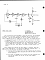
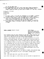
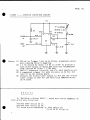
different low byte values in RE. Check that the control signals used
on the board (MRD,MWR,AO,A1) all appear correctly. Since there are
no data buss buffers on this board, no further checks of the buss
interface are necessary.
•
B-I/O Port Checks
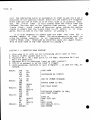
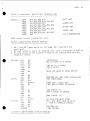
Install IC5 on the board. Using the program in Listing 2, exercise the I/O Port. Check that all 24 lines (mapped as outputs for
this test) appear as both a 0 and a 1. If a problem appears, then
modify the test routine to exercise only the bad lines and their
adjacent pins and PCB runs in different ways. The problem is most
likely an open or shorted connection on the PCB and can be quickly
tracked down by observing the pattern of the errors produced. Be
sure also the test the I/O lines right at the point where the IC
pins go into the IC package, as well as on the associated PCB connections.
If IC6 is to be used, install it now and repeat the above test.
Be sure to add 4 to the low byte of all I/O addresses used in Listing 2, so as to address the correct IC.
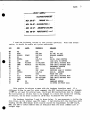
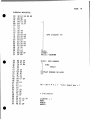
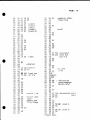
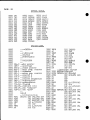
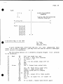
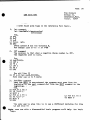
Listing 1- Address Decoding and Read Check:
LOOP1:
LDI
PHI
LDI
PLO
LDN
BR
OFF
RE
1100
RE
RE
LOOP1
;SETUP RE TO POINT TO MEMORY-MAPPED
I/O PAGE,
AND ANALOG OUTPUT BOARD
•
;READ THE BOARD REPEATEDLY
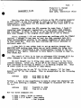
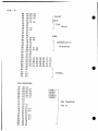
Listing 2- 8255 I/O Port Output Test
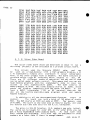
LOOP2
LDI
PH I
LDI
PLO
LDI
STR
LDI
PLO
LDI
STR
DEC
STR
DEC
STR
LDI
PLO
LDI
STR
IIFF
RA
1103
RA
1180
RA
1102
;SETUP RA TO POINT TO MEMORY-MAPPED
, I/O PAGE
AND ANALOG OUTPUT BOARD,
,
I/O PORT CONTROL BYTE
;INIT.' I/O PORT AS ALL OUTPUTS
;POINT TO PORT C
RA
IIFF
RA
RA
RA
RA
RA
/102
RA
1100
RA
;STORE FF INTO
PORT C,
PORT B,
,
AND PORT A.
;POINT TO PORT C AGAIN
;STORE 00 INTO
PORT C,
•