1
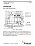
Freescale Semiconductor
Product Brief
DSP56301
24-Bit Digital Signal Processor
The DSP56301 is a member of the DSP56300 core family of programmable CMOS DSPs. This family uses a highperformance, single clock cycle per instruction engine. Significant architectural features of the DSP56300 core
family include a barrel shifter, 24-bit addressing, instruction cache, and DMA. The DSP56301 performs at
66/80/100 MIPS using an internal 66/80/100 MHz clock at 3.0–3.6 volts. The DSP56300 core family offers a rich
instruction set and low power dissipation, as well as increasing levels of speed and power, enabling wireless,
telecommunications, and multimedia products.
52
6
6
3
Memory Expansion Area
Peripheral
Expansion Area
Address
Generation
Unit
Six Channel
DMA Unit
X Data
RAM
2048 × 24
YAB
XAB
PAB
DAB
Y Data
RAM
2048 × 24
YM_EB
SCI
Interface
XM_EB
ESSI
Interface
PM_EB
Host
Interface
PIO_EB
Triple
Timer
Program RAM
4096 × 24
or
(3072 × 24 and
Instruction
Cache
1024 × 24)
24-Bit
DSP56300
Core
Bootstrap
ROM
External
Address
Bus
Switch
24
ADDRESS
External
Bus
14
Interface
&
I - Cache CONTROL
Control
DDB
YDB
Internal
Data
Bus
Switch
External
Data Bus
Switch
XDB
PDB
XTAL
PLL
2
RESET
PINIT/NMI
DATA
GDB
EXTAL
Clock
Generator
24
Program
Interrupt
Controller
Program
Decode
Controller
Program
Address
Generator
Data ALU
24 × 24+56→56-bit MAC
Two 56-bit Accumulators
56-bit Barrel Shifter
MODD/IRQD
MODC/IRQC
MODB/IRQB
MODA/IRQA
Figure 1. DSP56301 Block Diagram
© Freescale Semiconductor, Inc., 1996, 2005. All rights reserved.
Power
Mngmnt
JTAG
OnCE™
6
Because of an order from the United States International Trade Commission, BGA-packaged product lines and part numbers indicated here currently are not
available from Freescale for import or sale in the United States prior to September 2010: DSP56301
DSP56301PB
Rev. 2, 11/2005
DSP56301 Features
•
•
•
•
•
High-performance DSP56300 core
— 66/80/100 Million Instructions Per Second (MIPS) with a 66/80/100 MHz clock at 3.3 V
— Object code compatible with the DSP56000 core
— Highly parallel instruction set
— Fully pipelined 24 x 24-bit parallel multiplier-accumulator
— 56-bit parallel barrel shifter
— 24-bit or 16-bit arithmetic support under software control
— Position independent code support
— Addressing modes optimized for DSP applications
— On-chip instruction cache controller
— On-chip memory-expandable hardware stack
— Nested hardware DO loops
— Fast auto-return interrupts
— On-chip concurrent six-channel DMA controller
— On-chip Phase Lock Loop (PLL) and clock generator
— On-Chip Emulation (OnCE™) module
— Joint Action Test Group (JTAG) Test Access Port (TAP)
— Address tracing mode that reflects internal accesses at the external port
On-chip memories
— Program RAM, Instruction Cache, X data RAM, and Y data RAM size are programmable:
Instruction
Cache
Switch
Mode
Program
RAM Size
Instruction
Cache Size
X Data RAM
Size
Y Data Ram
Size
disabled
disabled
4096 × 24-bit
0
2048 × 24-bit
2048 × 24-bit
enabled
disabled
3072 × 24-bit
1024 × 24-bit
2048 × 24-bit
2048 × 24-bit
disabled
enabled
2048 × 24-bit
0
3072 × 24-bit
3072 × 24-bit
enabled
enabled
1024 × 24-bit
1024 × 24-bit
3072 × 24-bit
3072 × 24-bit
— 192 × 24-bit bootstrap ROM
Off-chip memory expansion
— Data memory expansion to two 16 M x 24-bit word memory spaces
— Program memory expansion to one 16 M x 24-bit word memory space
— External memory expansion port
— Chip Select Logic requiring no additional circuitry to interface to SRAMs and SSRAMs
— On-chip DRAM controller that requires no additional circuitry to interface to DRAMs
On-chip peripherals
— 32-bit parallel PCI/Universal Host Interface (HI32), PCI Rev. 2.1 compliant with no additional interface logic
required for other DSP563xx buses
— ISA interface requires only 74LS45-style buffer
— Two Enhanced Synchronous Serial Interfaces (ESSI)
— Serial Communications Interface (SCI) with baud rate generator
— Triple timer module
— Up to 42 programmable General Purpose I/O pins (GPIO), depending on which peripherals are enabled
Reduced power dissipation
— Very low power CMOS design
— Wait and Stop low power standby modes
— Fully-static logic, operation frequency down to 0 Hz (DC)
— Optimized power management circuitry
DSP56301 Product Brief, Rev. 2
2
Freescale Semiconductor
Because of an order from the United States International Trade Commission, BGA-packaged product lines and part numbers indicated here currently are not
available from Freescale for import or sale in the United States prior to September 2010: DSP56301
DSP56301 Features
Target Applications
The DSP56301 is intended as for general-purpose digital signal processing, particularly in multimedia and
telecommunication applications, such as videoconferencing and cellular telephony.
Product Documentation
The documents listed in Table 1 are required for a complete description of the DSP56301 and are necessary to
design with the part properly. Documentation is available from a local Freescale distributor, a Freescale
semiconductor sales office, a Freescale Literature Distribution Center, or the Freescale web site listed on the back
cover of this document.
Table 1. DSP56301 Documentation
Topic
Description
Order Number
DSP56300 Family Manual
Detailed description of the DSP56300 family
architecture and the 24-bit core processor and
instruction set
DSP56300FM
DSP56301 User’s Manual
Detailed description of DSP56301 memory,
peripherals, and interfaces
DSP56301UM
DSP56301 Technical Data
DSP56301 pin and package descriptions;
electrical and timing specifications
DSP56301
DSP56301 Product Brief, Rev. 2
Freescale Semiconductor
3
Because of an order from the United States International Trade Commission, BGA-packaged product lines and part numbers indicated here currently are not
available from Freescale for import or sale in the United States prior to September 2010: DSP56301
Target Applications
Home Page:
www.freescale.com
E-mail:
[email protected]
USA/Europe or Locations not listed:
Freescale Semiconductor
Technical Information Center, CH370
1300 N. Alma School Road
Chandler, Arizona 85224
+1-800-521-6274 or +1-480-768-2130
[email protected]
Europe, Middle East, and Africa:
Freescale Halbleiter Deutschland GMBH
Technical Information Center
Schatzbogen 7
81829 München, Germany
+44 1296 380 456 (English)
+46 8 52200080 (English)
+49 89 92103 559 (German)
+33 1 69 35 48 48 (French)
[email protected]
Japan:
Freescale Semiconductor Japan Ltd.
Headquarters
ARCO Tower 15F
1-8-1, Shimo-Meguro, Meguro-ku,
Tokyo 153-0064, Japan
0120 191014 or +81 3 5437 9125
[email protected]
Asia/Pacific:
Freescale Semiconductor Hong Kong Ltd.
Technical Information Center
2 Dai King Street
Tai Po Industrial Estate
Tai Po, N.T. Hong Kong
+800 2666 8080
[email protected]
For Literature Requests Only:
Freescale Semiconductor Literature Distribution Center
P.O. Box 5405
Denver, Colorado 80217
1-800-441-2447 or 303-675-2140
Fax: 303-675-2150
[email protected]
DSP56301PB
Rev. 2
2/2005
Information in this document is provided solely to enable system and software implementers to
use Freescale Semiconductor products. There are no express or implied copyright licenses
granted hereunder to design or fabricate any integrated circuits or integrated circuits based on
the information in this document.
Freescale Semiconductor reserves the right to make changes without further notice to any
products herein. Freescale Semiconductor makes no warranty, representation or guarantee
regarding the suitability of its products for any particular purpose, nor does Freescale
Semiconductor assume any liability arising out of the application or use of any product or
circuit, and specifically disclaims any and all liability, including without limitation consequential
or incidental damages. “Typical” parameters which may be provided in Freescale
Semiconductor data sheets and/or specifications can and do vary in different applications and
actual performance may vary over time. All operating parameters, including “Typicals” must be
validated for each customer application by customer’s technical experts. Freescale
Semiconductor does not convey any license under its patent rights nor the rights of others.
Freescale Semiconductor products are not designed, intended, or authorized for use as
components in systems intended for surgical implant into the body, or other applications
intended to support or sustain life, or for any other application in which the failure of the
Freescale Semiconductor product could create a situation where personal injury or death may
occur. Should Buyer purchase or use Freescale Semiconductor products for any such
unintended or unauthorized application, Buyer shall indemnify and hold Freescale
Semiconductor and its officers, employees, subsidiaries, affiliates, and distributors harmless
against all claims, costs, damages, and expenses, and reasonable attorney fees arising out of,
directly or indirectly, any claim of personal injury or death associated with such unintended or
unauthorized use, even if such claim alleges that Freescale Semiconductor was negligent
regarding the design or manufacture of the part.
Freescale™ and the Freescale logo are trademarks of Freescale Semiconductor, Inc. All other
product or service names are the property of their respective owners.
© Freescale Semiconductor, Inc. 1996, 2005.
Because of an order from the United States International Trade Commission, BGA-packaged product lines and part numbers indicated here currently are not
available from Freescale for import or sale in the United States prior to September 2010: DSP56301
How to Reach Us: