1
DEVELOPMENT TOOLS
The
Insider’s Guide
To The
NXP LPC2300/2400
Based Microcontrollers
An Engineer’s Introduction To The LPC2300 & LPC2400 Series
www.hitex.co.uk
Published by Hitex (UK) Ltd.
ISBN: 0-9549988 6
First Version 1.00, February 2007
Hitex (UK) Ltd.
Sir William Lyons Road
University of Warwick Science Park
Coventry, CV4 7EZ
Credits
Author:
Illustrator:
Editor:
Cover:
Trevor Martin
Sarah Latchford
Michael Beach
Wolfgang Fuller
Acknowledgements
The author would like to thank Kees van Seventer and Chris Davies of NXP Semiconductors for their assistance
in compiling this book.
© Hitex (UK) Ltd., 06/02/2007
All rights reserved. No part of this publication may be reproduced, stored in a retrieval system or transmitted in
any form or by any means, electronic, mechanical or photocopying, recording or otherwise without the prior
written permission of the Publisher.
Introduction
This book is intended as a hands-on guide for anyone planning to use the NXP LPC2300 and LPC2400 family
of microcontrollers in a new design. It is laid out both as a reference book and as a tutorial. It is assumed that
you have some experience in programming microcontrollers for embedded systems, and are familiar with the C
language. The bulk of technical information is spread over the first four chapters, which should be read in order
if you are completely new to the LPC2300/2400 and the ARM7 CPU. Please note that in this book the LPC2300
will be used as a basis, with any LPC2400 differences highlighted separately.
The first chapter gives an introduction to the major features of the ARM7 CPU. Reading this chapter will give
you enough understanding to be able to program any ARM7 device. If you want to develop your knowledge
further, there are a number of excellent books that describe this architecture. Some of these are listed in the
bibliography. Chapter 2 is a description of how to write C programs to run on an ARM7 processor and, as such,
describes specific extensions to the ISO C standard that are necessary for embedded programming. In this
book a commercial compiler is used in the main text, however the GCC tools have also been ported to ARM.
Having read the first two chapters, you should understand the processor and its development tools. Chapter 3
then introduces the LPC2300 system peripherals. This chapter describes the system architecture of the
LPC2300 family, and how to set the chip up for its best performance. In Chapter 4 we look at the on-chip user
peripherals and how to configure them for our application code. Chapter 5 describes the complex peripherals
like USB and Ethernet. Chapters 6 and 7 are concerned with using popular real time operating systems from
Keil and FreeRTOS.
Throughout these chapters various exercises are listed. Each of these exercises is described in detail in the
accompanying Worksheets PDF files and CD. The Tutorial contains a worksheet for each exercise, which steps
you through an important aspect of the LPC2300. All of the exercises can be done with the evaluation compiler
and simulator, which come on the CD provided with this book. A low-cost starter kit is also available, which
allows you to download the example code on to some real hardware and “prove” that it does in fact work. It is
hoped that by reading the book and doing the exercises you will quickly become familiar with the LPC2300 and
LPC2400.
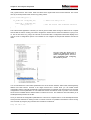
Contents
1
1.1
1.2
1.3
1.4
1.5
1.6
1.6.1
1.6.2
1.6.2.1
1.6.2.2
1.7
1.8
1.9
1.10
1.11
1.12
Chapter 1: The ARM7 CPU Core
12
Outline ......................................................................................................12
The Pipeline..............................................................................................12
Registers ..................................................................................................13
Current Program Status Register .............................................................14
Exception Modes ......................................................................................15
The ARM7 Instruction Set.........................................................................18
Branching .................................................................................................20
Data Processing Instructions ....................................................................21
Copying Registers ....................................................................................22
Copying Multiple Registers .......................................................................22
Swap Instruction .......................................................................................23
Modifying the Status Registers .................................................................23
Software Interrupt .....................................................................................24
MAC Unit ..................................................................................................25
THUMB Instruction Set .............................................................................26
Summary ..................................................................................................28
2
2.1
2.1.1
2.1.2
2.1.3
2.1.4
2.2
2.2.1
2.2.2
2.3
2.3.1
2.4
2.4.1
2.5
2.5.1
2.6
2.6.1
2.6.2
2.6.3
2.6.4
2.6.5
2.6.6
2.6.7
2.6.8
2.7
2.7.1
2.8
2.8.1
2.8.2
2.9
2.9.1
2.9.2
2.10
Chapter 2: Software Development
30
Outline ......................................................................................................30
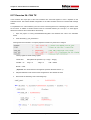
Downloading And Installing The Keil Tools...............................................30
uVision IDE...............................................................................................31
HiTOP IDE................................................................................................32
The Tutorials.............................................................................................33
Interworking ARM/THUMB Code ..............................................................34
Defining The Project Memory Map ...........................................................37
Defining The Memory Map With The GCC Compiler ................................37
Interworking ARM/THUMB Code ..............................................................40
Interworking With The GCC Compiler.......................................................41
STDIO Libraries ........................................................................................42
STDIO With The GCC Compiler ...............................................................42
Accessing Peripherals ..............................................................................43
Accessing Peripherals With The GCC Compiler.......................................43
Interrupt Service Routines ........................................................................44
Interrupt Handling With The GCC Compiler..............................................45
Debugging The Error Exception Handlers ................................................46
Software Interrupt .....................................................................................46
Software Interrupts In The GCC Compiler ................................................47
Locating Variables At Absolute Memory Locations...................................48
Locating Code In RAM..............................................................................48
Using The GCC Compiler To Load Code And Data Into RAM..................49
Debug Information When In RAM .............................................................52
Inline Functions ........................................................................................53
Inline Functions With The GCC Compiler .................................................53
Inline Assembler .......................................................................................54
Inline Assembler With The GCC Compiler................................................54
Importing GCC Code ................................................................................54
Hardware Debugging Tools ......................................................................55
Important! .................................................................................................55
Even More Important ................................................................................56
Summary ..................................................................................................56
3
Chapter 3: System Peripherals
58
3.1
3.2
3.3
3.4
3.5
3.5.1
3.6
3.6.1
3.6.2
3.6.3
3.6.4
3.6.5
3.6.6
3.6.7
3.6.8
3.7
3.7.1
3.7.2
3.7.2.1
3.7.2.2
3.7.2.3
3.7.2.4
3.7.2.5
3.8
3.8.1
3.8.2
3.8.3
3.8.4
3.8.5
3.8.5.1
3.8.6
3.8.7
3.8.8
3.8.9
3.8.10
3.9
3.9.1
3.9.2
3.9.3
3.9.4
3.9.5
3.9.6
3.10
Outline ......................................................................................................58
Bus Structure............................................................................................58
Memory Map.............................................................................................59
Register Programming..............................................................................60
Memory Accelerator Module.....................................................................60
Example MAM Configuration ....................................................................63
FLASH Memory Programming..................................................................64
Memory Map Control ................................................................................64
Bootloader ................................................................................................65
NXP ISP Utility..........................................................................................65
In-Application Programming .....................................................................67
FLASH Protection .....................................................................................68
System Clocks ..........................................................................................69
Phase Locked Loop ..................................................................................70
Peripheral Clocks......................................................................................72
Power Control ...........................................................................................73
Power Domains ........................................................................................73
Global Power Control Modes ....................................................................73
Idle Mode..................................................................................................73
Sleep Mode ..............................................................................................73
Power down..............................................................................................74
Deep Power Down....................................................................................74
Peripheral Power Control..........................................................................74
LPC2300 Interrupt System .......................................................................76
Pin Connect Block ....................................................................................76
External Interrupt Pins ..............................................................................76
Interrupt Structure.....................................................................................77
FIQ Interrupt .............................................................................................77
Leaving an FIQ Interrupt...........................................................................78
Example Program: FIQ Interrupt..............................................................79
Vectored IRQ ............................................................................................80
Leaving An IRQ Interrupt ..........................................................................81
Example Program: IRQ Interrupt ..............................................................81
Software Interrupt .....................................................................................83
Nested Interrupts ......................................................................................84
DMA Controller .........................................................................................85
DMA Overview..........................................................................................85
DMA Synchronisation ...............................................................................86
Memory to Memory Transfer ....................................................................86
Burst Transfer...........................................................................................87
Peripheral DMA Support...........................................................................87
Scatter Gather Transfer ............................................................................88
Summary ..................................................................................................88
4
4.1
4.2
4.2.1
4.2.2
4.3
4.3.1
4.3.2
4.3.3
4.4
Chapter 4: User Peripherals
90
Outline ......................................................................................................90
General Purpose I/O.................................................................................90
Fast IO Registers......................................................................................90
Interrupt Port.............................................................................................92
General Purpose Timers...........................................................................93
Capture Mode ...........................................................................................93
Counter mode ...........................................................................................94
Match mode ..............................................................................................94
PWM Modulator ........................................................................................97
4.4.1
4.5
4.5.1
4.6
4.6.1
4.7
4.7.1
4.7.2
4.7.3
4.7.4
4.8
4.9
4.10
4.11
4.12
4.12.1
4.13
4.13.1
Counter Mode ...........................................................................................99
Real Time Clock .....................................................................................100
RTC Time Reference..............................................................................100
Watchdog ...............................................................................................103
Watchdog Timeout..................................................................................103
UART......................................................................................................105
Baud Rate Configuration ........................................................................105
Auto Baud Rate Detection ......................................................................106
Data Transfer..........................................................................................107
IrDA Communication...............................................................................109
I2C Interface ...........................................................................................110
SPI Interface...........................................................................................115
Analog To Digital Converter....................................................................117
Digital To Analog Converter....................................................................120
Synchronous Peripheral Controller .........................................................121
I2S Controller..........................................................................................124
SD-MMC Card Interface .........................................................................126
SD_MMC Register Set ...........................................................................127
5
5.1
5.2
5.2.1
5.2.2
5.2.3
5.2.3.1
5.2.3.2
5.2.3.3
5.2.3.4
5.2.3.5
5.2.3.6
5.2.4
5.2.4.1
5.2.4.2
5.2.4.3
5.2.4.4
5.2.4.5
5.2.4.6
5.2.5
5.2.5.1
5.2.5.2
5.2.5.3
5.2.5.4
5.2.5.5
5.2.6
5.2.6.1
5.2.6.2
5.2.6.3
5.2.6.4
5.2.6.5
5.3
5.3.1
5.3.1.1
5.3.2
The Complex Peripherals
129
Ethernet MAC .........................................................................................129
TCP/IP ....................................................................................................129
Network Model........................................................................................129
Ethernet And IEEE 802.3.......................................................................129
TCP/IP Datagrams..................................................................................130
Internet Protocol .....................................................................................131
Address Routing Protocol .......................................................................131
Subnet mask...........................................................................................132
Internet Message Control Protocol (IMCP) .............................................132
Transmission Control Protocol (TCP) .....................................................132
User Datagram Protocol (UDP) ..............................................................133
LPC23xx Ethernet Peripheral ................................................................133
MAC Configuration .................................................................................134
The MII Interface.....................................................................................135
DMA Configuration .................................................................................138
Receive Filtering .....................................................................................141
Power Management................................................................................142
Performance ...........................................................................................143
uIP Stack ................................................................................................144
Configuring The Stack ............................................................................144
Packet Handling .....................................................................................144
Maintaining TCP And UDP Connections ................................................145
Maintaining The ARP Cache ..................................................................146
Application Protocols ..............................................................................146
Building A Webserver With A Commercial TCP/IP stack........................147
The Bare Bones Project..........................................................................147
Adding Some Web Pages.......................................................................149
The Common Gateway Interface ............................................................151
Post Method ...........................................................................................151
Dynamic HTML .......................................................................................152
USB 2.0 Full Speed Slave Peripheral .....................................................156
Introduction to USB.................................................................................156
USB Physical Network............................................................................156
LPC2300 USB Peripheral .......................................................................167
5.4
5.5
5.5.1.1
5.5.2
5.5.3
5.5.4
5.5.5
5.5.6
5.5.7
5.5.8
5.5.9
5.5.9.1
5.5.9.2
Summary ................................................................................................174
CAN Controller .......................................................................................175
ISO 7 Layer Model..................................................................................175
CAN Node Design ..................................................................................175
CAN Message Objects ...........................................................................177
CAN Bus Arbitration................................................................................178
Bit Timing................................................................................................179
CAN Message Transmission ..................................................................180
CAN Error Containment..........................................................................182
CAN Message Reception .......................................................................185
Acceptance Filtering ...............................................................................186
Configuring The Acceptance Filter .........................................................186
Full CAN Mode .......................................................................................188
6
6.1
6.2
6.3
6.4
6.5
6.6
6.7
6.8
6.8.1
6.8.2
6.8.3
6.8.4
6.9
6.9.1
6.9.2
6.9.3
6.9.4
6.9.5
6.9.6
6.9.7
6.10
Chapter 6: Using The Keil Real Time Executive
191
Features .................................................................................................191
Setting Up A Project ...............................................................................192
Tasks ......................................................................................................193
Starting The RTOS .................................................................................195
Creating Tasks .......................................................................................196
Task Management ..................................................................................197
Multiple Instances ...................................................................................197
Time Management..................................................................................198
Time Delay .............................................................................................198
Periodic Task Execution .........................................................................198
Virtual Timer ...........................................................................................198
Idle Demon .............................................................................................199
Intertask Communication ........................................................................200
Events.....................................................................................................200
RTOS Interrupt Handling ........................................................................201
Semaphores ...........................................................................................202
Semaphore Caveats ...............................................................................203
Mutex......................................................................................................203
Mutex Caveats........................................................................................203
Mailbox ...................................................................................................203
Configuration ..........................................................................................207
7
7.1
7.1.1
7.1.2
7.1.3
7.1.4
7.1.5
7.2
7.2.1
7.2.2
7.2.3
7.2.3.1
7.2.3.2
7.2.3.3
7.2.3.4
7.2.3.5
7.2.4
Chapter 7: Using The FreeRTOS Real Time Executive
209
Porting FreeRTOS To The LPC2300......................................................209
Timer Tick...............................................................................................209
Timer ISR ...............................................................................................211
Context switching ...................................................................................211
Initialise Stack.........................................................................................212
Memory Management.............................................................................214
Free RTOS Configuration .......................................................................214
Starting FreeRTOS .................................................................................215
Tasks ......................................................................................................216
Task Management ..................................................................................217
Time Management..................................................................................217
Suspend/Resume ...................................................................................217
Resuming A Task From An ISR..............................................................218
Changing Priority Levels.........................................................................218
Idle Task .................................................................................................219
Tick Hook................................................................................................219
7.2.5
7.2.5.2
7.2.6
7.2.6.1
Semaphores ...........................................................................................219
Message Queues....................................................................................220
Kernel Control.........................................................................................222
Critical Code Sections ............................................................................222
8
8.1
8.2
8.3
8.4
8.4.2
8.4.3
8.4.4
8.4.5
8.4.5.1
8.4.6
8.4.7
8.4.8
8.5
8.6
8.7
8.8
8.9
8.10
8.11
8.12
8.13
8.14
8.15
8.16
8.17
8.18
8.19
8.20
8.21
8.22
8.23
8.24
8.25
8.26
8.27
8.28
8.29
8.30
8.31
8.32
8.33
8.34
8.35
8.36
Chapter 8: Tutorial Examples
223
Introduction.............................................................................................223
Exercise 0: Installing The Software ........................................................224
Setting Up The Hardware .......................................................................225
Exercise 1 With The HiTOP Toolchain. ..................................................226
HiTOP Debugger ....................................................................................226
Getting To Main()....................................................................................229
Editing Your Project ................................................................................229
Run Control ............................................................................................230
Viewing Data ..........................................................................................234
HiTOP Project Settings...........................................................................236
Advanced Breakpoints............................................................................237
Exception Assistant ................................................................................239
HiSCRIPT Script Language ....................................................................240
Exercise 2: Startup Code.......................................................................242
Exercise 3: Interworking ARM & THUMB Instruction Sets......................246
Exercise 4: Software Interrupt ................................................................248
Exercise 5: System Clock .......................................................................249
Exercise 6: Phase Locked Loop .............................................................250
Exercise 7: Memory Accelerator Module ................................................252
Exercise 8: Using The NXP Bootloader ..................................................253
Exercise 9: Fast Interrupt........................................................................255
Exercise 10: Vectored Interrupt ..............................................................257
Exercise 11: Memory to Memory DMA Transfer .....................................259
Exercise 12: Scatter-Gather DMA Transfer ............................................261
Exercise 13: GPIO ..................................................................................262
Exercise 14: GPIO Port Interrupt ............................................................263
Exercise 15: Timer Match .......................................................................265
Exercise 16: Timer Capture ....................................................................267
Exercise 17: PWM ..................................................................................268
Exercise 18: RTC....................................................................................269
Exercise 19: UART .................................................................................271
Exercise 20: ADC ...................................................................................272
Exercise 21: DAC ...................................................................................273
Exercise 22: Ethernet Driver...................................................................274
Exercise 23: uIP TCP/IP Stack ...............................................................276
Exercise 24: CAN TX..............................................................................278
Exercise 25: CAN RX .............................................................................280
Exercise 26: Full CAN Reception ...........................................................282
Exercise 27: 2 Tasks ..............................................................................284
Exercise 28: Time Management .............................................................286
Exercise 29: Suspend.............................................................................287
Exercise 30: Resume ISR.......................................................................288
Exercise 31: Idle Task ............................................................................289
Exercise 32: Semaphore ........................................................................290
Exercise 33: Queue ................................................................................291
9
9.1
Appendices
293
Appendix A .............................................................................................293
8.4.1
9.1.1
9.1.2
9.1.2.1
9.1.3
9.2
Bibliography............................................................................................293
Webliography..........................................................................................293
Reference Sites ......................................................................................293
Tools and Software Development...........................................................293
Evaluation Boards And Modules.............................................................293
Chapter 1: The ARM7 CPU
© Hitex (UK) Ltd.
Page 11
Chapter 1: The ARM7 CPU
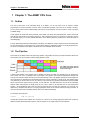
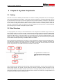
1 Chapter 1: The ARM7 CPU Core
1.1 Outline
The CPU at the heart of the LPC2300 family is an ARM7. You do not need to be an expert in ARM7
programming to use the LPC2300, as many of the complexities are taken care of by the C compiler. However,
you do need to have a basic understanding of the CPU’s unique features and how it works, in order to produce
a reliable design.
In this chapter we will look at the key features of the ARM7 core along with its programmers’ model, and we will
also discuss the instruction set used to program it. This is intended to give you a good feel for the CPU used in
the LPC2300 family. For a more detailed discussion of the ARM processors, please refer to the books listed in
the bibliography.
The key philosophy behind the ARM design is simplicity. The ARM7 is a RISC computer with a small instruction
set and consequently a small gate count. This makes it ideal for embedded systems. It has high performance,
low power consumption and it takes a small amount of the available silicon die area.
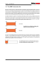
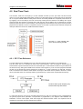
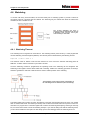
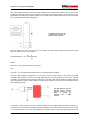
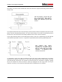
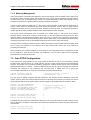
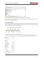
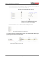
1.2 The Pipeline
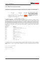
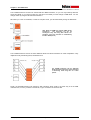
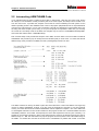
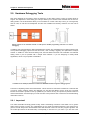
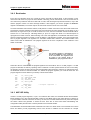
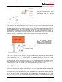
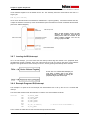
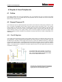
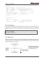
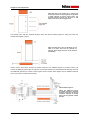
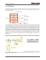
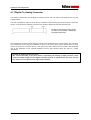
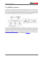
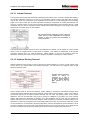
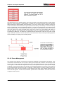
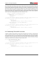
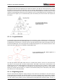
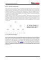
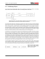
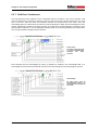
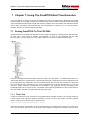
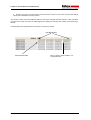
At the heart of the ARM7 CPU is the instruction pipeline. The pipeline is used to process instructions taken from
the program store. On the ARM 7 a three-stage pipeline is used.
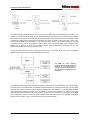
The ARM7 three-stage pipeline
has independent Fetch, Decode
and Execute stages.
A three-stage pipeline is the simplest form of pipeline and does not suffer from hazards such as read-beforewrite, which can occur in pipelines with more stages. The pipeline has hardware-independent stages that
execute one instruction while decoding a second and fetching a third. The pipeline speeds up the throughput of
CPU instructions so effectively that most ARM instructions can be executed in a single cycle. The pipeline works
most efficiently on linear code. As soon as a branch is encountered, the pipeline is flushed and must be refilled
before full execution speed can be resumed. As we shall see, the ARM instruction set has some interesting
features which help smooth out small jumps in your code in order to get the best flow of code through the
pipeline. As the pipeline is part of the CPU, the programmer does not have any exposure to it. However, it is
important to remember that the PC is running eight bytes ahead of the current instruction being executed, so
care must be taken when calculating offsets used in PC relative addressing.
For example, the instruction:
0x4000
LDR PC,[PC,#4]
will load the contents of the address PC+4 into the PC. As the PC is running eight bytes ahead, the contents of
address 0x400C will be loaded into the PC and not 0x4004 as you might expect on first inspection.
© Hitex (UK) Ltd.
Page 12
Chapter 1: The ARM7 CPU
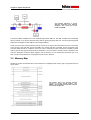
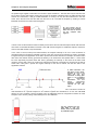
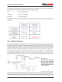
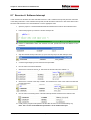
1.3 Registers
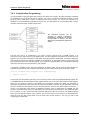
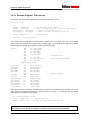
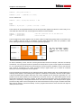
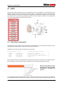
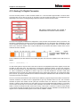
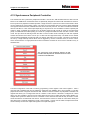
The ARM7 is a load-and-store architecture, so in order to perform any data processing instructions the data has
first to be moved from the memory store into a central set of registers, then the data processing instruction has
to be executed, and then the data is stored back into memory.
The ARM7 CPU is a load-andstore architecture. All data
processing instructions may
only be carried out on a central
register file.
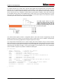
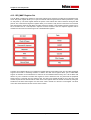
The central set of registers is a bank of 16 user registers: R0 – R15. Each of these registers is 32 bits wide and
R0 – R12 are User registers in that they do not have any other specific function. The registers R13 – R15 do
have special functions in the CPU. R13 is used as the Stack Pointer (SP). R14 is called the Link Register (LR).
When a call is made to a function, the return address is automatically stored in the Link Register and is
immediately available on return from the function. This allows quick entry and return into a ‘leaf’ function (a
function that is not going to call further functions). If the function is part of a branch (i.e. it is going to call other
functions) then the Link Register must be preserved on the Stack (R13). Finally R15 is the Program Counter
(PC). Interestingly, many instructions can be performed on R13 - R15 as if they were standard User registers.
The central register file has 16 word wide registers plus
an additional CPU register called the Current Program
Status Register. R0 – R12 are User registers. R13 – R15
have special functions.
© Hitex (UK) Ltd.
Page 13
Chapter 1: The ARM7 CPU
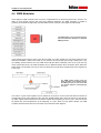
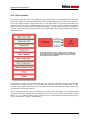
1.4 Current Program Status Register
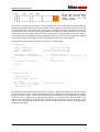
In addition to the register bank there is an additional 32 bit wide register called the ‘Current Program Status
Register’ (CPSR). The CPSR contains a number of flags which report and control the operation of the ARM7
CPU.
The Current Program Status Register contains condition code flags which indicate the result of
data processing operations and User flags which set the operating mode and enable interrupts.
The T bit is for reference only.
The top four bits of the CPSR contain the condition codes which are set by the CPU. The condition codes report
the result status of a data processing operation. From the condition codes you can tell if a data processing
instruction generated a Negative, Zero, Carry or Overflow result. The lowest eight bits in the CPSR contain flags
which may be set or cleared by the application code. Bits 7 and 8 are the I and F bits. These bits are used to
enable and disable the two interrupt sources which are external to the ARM7 CPU. All of the LPC2300
peripherals are connected to these two interrupt lines, as we shall see later. You should be careful when
programming these two bits because in order to disable either interrupt source, the bit must be set to ‘1’ not ‘0’
as you might expect. Bit 5 is the THUMB bit.
The ARM7 CPU is capable of executing two instruction sets: the ARM instruction set which is 32 bits wide, and
the THUMB instruction set which is 16 bits wide. Consequently the T bit reports which instruction set is being
executed. Your code should not try to set or clear this bit to switch between instruction sets. We will see the
correct entry mechanism a bit later. The last five bits are the mode bits. The ARM7 has seven different
operating modes. Your application code will normally run in the User Mode with access to the register bank R0
– R15 and the CPSR as already discussed. However, in response to an exception such as an interrupt, memory
error or software interrupt instruction, the processor will change modes. When this happens the registers R0 –
R12 and R15 remain the same, but R13 (LR) and R14 (SP) are replaced by a new pair of registers unique to
that mode. This means that each mode has its own Stack and Link Register. In addition the Fast Interrupt Mode
(FIQ) has duplicate registers for R7 – R12. This means that you can make a fast entry into an FIQ interrupt
without the need to preserve registers onto the Stack.
© Hitex (UK) Ltd.
Page 14
Chapter 1: The ARM7 CPU
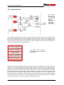
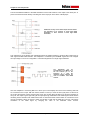
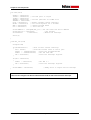
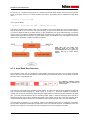
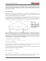
Each of the modes except User Mode has an additional register called the “Saved Program Status Register”. If
your application is running in User Mode when an exception occurs, the mode will change and the current
contents of the CPSR will be saved into the SPSR. The exception code will run and, on return from the
exception, the context of the CPSR will be restored from the SPSR, allowing the application code to resume
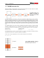
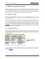
execution. The operating modes are listed below.
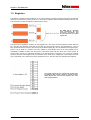
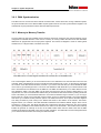
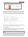
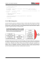
The ARM7 CPU has six operating modes
which are used to process exceptions. The
shaded registers are banked memory that
is “switched in” when the operating mode
changes. The SPSR register is used to
save a copy of the CPSR when the switch
occurs.
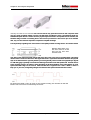
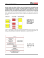
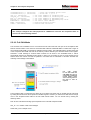
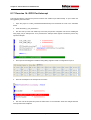
1.5 Exception Modes
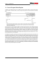
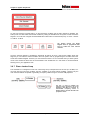
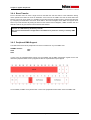
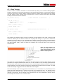
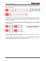
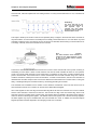
When an exception occurs, the CPU will change modes and the PC will be forced to an exception vector. The
vector table starts from address zero with the reset vector, and then has an exception vector every four bytes.
Each operating mode has an
associated interrupt vector. When
the processor changes mode the
PC will jump to the associated
vector.
NB: there is a missing vector at
0x00000014.
© Hitex (UK) Ltd.
Page 15
Chapter 1: The ARM7 CPU
NB: There is a gap in the vector table because there is a missing vector at 0x00000014. This location was used
on an earlier ARM architecture and has been preserved on ARM7 to ensure software compatibility between
different ARM architectures. However in the LPC2300 family these four bytes are used for a very special
purpose as we shall see later.
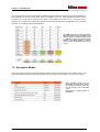
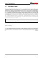
If multiple exceptions occur there is a fixed priority, as shown below.
Each of the exception sources has a fixed priority. The
on-chip peripherals are served by FIQ and IRQ
interrupts. Each peripheral’s priority may be assigned
within these groups.
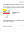
When an exception occurs, for example an IRQ exception, the following actions are taken. Firstly the address of
the next instruction to be executed (PC + 4) is saved into the Link Register. Then the CPSR is copied into the
SPSR of the Exception Mode that is about to be entered (i.e. “SPSR_irq”). The PC is then filled with the address
of the Exception Mode Interrupt Vector. In the case of the IRQ Mode this is 0x00000018. At the same time the
mode is changed to IRQ Mode, which causes R13 and R14 to be replaced by the IRQ R13 and R14 registers.
On entry to the IRQ Mode, the I bit in the CPSR is set, causing the IRQ interrupt line to be disabled. If you need
to have nested IRQ interrupts, your code must manually re-enable the IRQ interrupt and push the Link Register
onto the Stack in order to preserve the original return address. From the Exception Interrupt Vector your code
will jump to the exception ISR. The first thing your code must do is to preserve any of the registers R0 - R12 that
the ISR will use by pushing them onto the IRQ Stack. Once this is done you can begin processing the
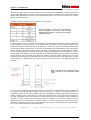
exception.
When an exception occurs the CPU will change
modes and jump to the associated interrupt
vector.
Once your code has finished processing the exception it must return to the User Mode and continue where it left
off. However, the ARM instruction set does not contain a “return” or “return from interrupt” instruction, so
manipulating the PC must be done by regular instructions. The situation is further complicated by there being a
number of different return cases. First of all, consider the SWI instruction. In this case the SWI instruction is
executed, the address of the next instruction to be executed is stored in the Link Register and the exception is
processed. In order to return from the exception, all that is necessary is to move the contents of the Link
Register into the PC and processing can continue. However, in order to make the CPU switch modes back to
User Mode, a modified version of the move instruction is used and this is called MOVS (more about this later).
Hence, for a software interrupt the return instruction is:
MOVS
© Hitex (UK) Ltd.
R15,R14
; Move Link register into the PC and switch modes.
Page 16
Chapter 1: The ARM7 CPU
However, in the case of the FIQ and IRQ instructions, when an exception occurs the current instruction being
executed is discarded and the exception is entered. When the code returns from the exception the Link Register
contains the address of the discarded instruction plus four. In order to resume processing at the correct point we
need to roll back the value in the Link Register by four. In this case we use the subtract instruction to deduct
four from the Link Register and store the results in the PC. As with the move instruction, there is a form of the
subtract instruction which will also restore the Operating Mode. For an IRQ, FIQ or Prefetch Abort, the return
instruction is:
SUBS
R15, R14,#4
In the case of a data abort instruction, the exception will occur one instruction after execution of the instruction
which caused the exception. In this case we will ideally enter the data abort ISR, sort out the problem with the
memory and return to reprocess the instruction that caused the exception. We have to roll back the PC by two
instructions, i.e. the discarded instruction and the instruction that caused the exception. In other words, subtract
eight from the Link Register and store the result in the PC. For a data abort exception the return instruction is:
SUBS
R15, R14,#8
Once the return instruction has been executed, the modified contents of the Link Register are moved into the
PC, the User Mode is restored and the SPSR is restored to the CPSR. Also, in the case of the FIQ or IRQ
exceptions, the relevant interrupt is enabled. This exits the Privileged Mode and returns to the User code ready
to continue processing.
At the end of the exception the CPU
returns to User Mode and the context is
restored by moving the SPSR to the CPSR.
© Hitex (UK) Ltd.
Page 17
Chapter 1: The ARM7 CPU
1.6 The ARM7 Instruction Set
Now that we have an idea of the ARM7 architecture, programmer’s model and operating modes, we need to
take a look at its instruction set, or rather, sets. Since all our programming examples are written in C there is no
need to be an expert ARM7 assembly programmer. However an understanding of the underlying machine code
is very important in developing efficient programs. Before we start our overview of the ARM7 instructions it is
important to set out a few technicalities. The ARM7 CPU has two instruction sets: the ARM instruction set which
has 32-bit wide instructions, and the THUMB instruction set which has 16-bit wide instructions. In the following
section the use of the word ARM means the 32-bit instruction set, and ARM7 refers to the CPU.
The ARM7 is designed to operate as a big-endian or little-endian processor. That is, the MSB is located at the
high order bit or the low order bit. You may be pleased to hear that the LPC2300 family fixes the endianism of
the processor as little-endian (i.e. MSB at highest bit address), which does make it a lot easier to work with.
However, the ARM7 compiler you are working with will be able to compile code as little-endian or big-endian.
You must be sure you have it set correctly or the compiled code will be back to front.
The ARM7 CPU is designed to support code
compiler in big-endian or little-endian format. The
Philips silicon is fixed as little-endian.
One of the most interesting features of the ARM instruction set is that every instruction may be conditionally
executed. In a more traditional microcontroller, the only conditional instructions are conditional branches and
maybe a few others like bit test and set. However, in the ARM instruction set the top four bits of the operand are
compared to the condition codes in the CPSR. If they do not match, then the instruction is not executed and
passes through the pipeline as a NOP (no operation).
Every ARM (32-bit) instruction is conditionally executed. The top
four bits are ANDed with the CPSR condition codes. If they do
not match, the instruction is executed as a NOP.
© Hitex (UK) Ltd.
Page 18
Chapter 1: The ARM7 CPU
So it is possible to perform a data processing instruction, which affects the condition codes in the CPSR. Then
depending on this result, the following instructions may or may not be carried out. The basic assembler
instructions such as MOV or ADD can be prefixed with sixteen conditional mnemonics, which define the
condition code states to be tested for.
Each ARM (32-bit) instruction can
be prefixed by one of 16 condition
codes. Hence each instruction has
16 different variants.
So for example:
The instruction:
EQMOV R1, #0x00800000
will only move 0x00800000 into the R1 if the last result of the last data processing instruction was equal and
consequently set the Z flag in the CPSR. The aim of this conditional execution of instructions is to keep a
smooth flow of instructions through the pipeline. Every time there is a branch or jump the pipeline is flushed and
must be refilled, and this causes a dip in overall performance. In practice there is a break-even point between
effectively forcing NOP instructions through the pipeline and a traditional conditional branch and refill of the
pipeline. This break-even point is three instructions, so a small branch such as:
if( x<100)
{
x++;
}
would be most efficient when coded using conditional execution of ARM instructions.
The main instruction groups of the ARM instruction set fall into six different categories: Branching, Data
Processing, Data Transfer, Block Transfer, Multiply and Software Interrupt.
© Hitex (UK) Ltd.
Page 19
Chapter 1: The ARM7 CPU
1.6.1 Branching
The basic branch instruction (as its name implies) allows a jump forwards or backwards of up to 32 MB. A
modified version of the branch instruction, the branch link, allows the same jump but stores the current PC
address plus four bytes in the Link Register.
Should be small ‘x’?
The branch instruction has several forms. The
basic branch instruction will jump you to a
destination address. The branch link instruction
jumps to the destination and stores a return
address in R14.
So the branch link instruction is used as a call to a function, storing the return address in the Link Register and
the branch instruction can be used to branch on the contents of the Link Register to make the return at the end
of the function. By using the condition codes we can perform conditional branching and conditional calling of
functions. The branch instructions have two other variants called “branch exchange” and “branch link
exchange”. These two instructions perform the same branch operation but also swap instruction operation from
ARM to THUMB and vice versa.
The branch exchange and branch link exchange
instructions perform the same jumps as branch and
branch link but also swap instruction sets from ARM to
THUMB and vice versa.
This is the only method you should use to swap instruction sets, as directly manipulating the “T” bit in the CPSR
can lead to unpredictable results.
© Hitex (UK) Ltd.
Page 20
Chapter 1: The ARM7 CPU
1.6.2 Data Processing Instructions
The general form for all data processing instructions is shown below. Each instruction has a Result Register and
two operands. The first operand must be a register, but the second can be a register or an immediate value.
The general structure of the
data processing instructions
allows for conditional execution,
a logical shift of up to 32 bits
and the data operation all in the
one cycle.
In addition, the ARM7 core contains a barrel shifter which allows the second operand to be shifted by a full 32
bits within the instruction cycle. The “S” bit is used to control the condition codes. If it is set, the condition codes
are modified depending on the result of the instruction. If it is clear, no update is made. If, however, the PC
(R15) is specified as the Result Register and the S flag is set, this will cause the SPSR of the current mode to
be copied to the CPSR. This is used at the end of an exception to restore the PC and switch back to the original
mode. Do not try this when you are in the User Mode as there is no SPSR and the result would be
unpredictable.
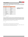
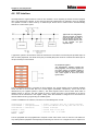
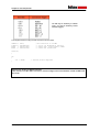
Mnemonic
Meaning
AND
EOR
SUB
RSB
ADD
ADC
SBC
RSC
TST
TEQ
CMP
CMN
ORR
MOV
BIC
MVN
Logical Bitwise AND
Logical Bitwise Exclusive OR
Subtract
Reverse Subtract
Add
Add with Carry
Subtract with Carry
Reverse Subtract with Carry
Test
Test Equivalence
Compare
Compare Negated
Logical Bitwise OR
Move
Bit Clear
Move Negated
These features give us a rich set of data processing instructions which can be used to build very efficientlycoded programs, or to give a compiler designer nightmares! An example of a typical ARM instruction is shown
below:
if(Z ==1)R1 = R2+(R3x4)
This can be compiled to:
EQADDS R1,R2,R3,LSL #2
© Hitex (UK) Ltd.
Page 21
Chapter 1: The ARM7 CPU
1.6.2.1
Copying Registers
The next group of instructions is the data transfer instructions. The ARM7 CPU has load-and-store register
instructions that can move signed and unsigned Word, Half Word and Byte quantities to and from a selected
register.
Mnemonic
Meaning
LDR
LDRH
LDRSH
LDRB
LRDSB
Load
Load
Load
Load
Load
STR
STRH
STRSH
STRB
STRSB
Store
Store
Store
Store
Store
Word
Half Word
Signed Half Word
Byte
Signed Byte
Word
Half Word
Signed Half Word
Byte
Signed Half Word
Since the register set is fully orthogonal it is possible to load a 32-bit value into the PC, forcing a program jump
anywhere within the processor address space. If the target address is beyond the range of a branch instruction,
a stored constant can be loaded into the PC.
1.6.2.2
Copying Multiple Registers
In addition to load-and-storing single register values, the ARM has instructions to load-and-store multiple
registers. So with a single instruction, the whole register bank or a selected subset can be copied to memory
and restored with a second instruction.
The load-and-store multiple instructions
allow you to save or restore the entire
register file or any subset of registers in a
single instruction.
© Hitex (UK) Ltd.
Page 22
Chapter 1: The ARM7 CPU
1.7 Swap Instruction
The ARM instruction set also provides support for real time semaphores with a swap instruction. The swap
instruction exchanges a word between registers and memory as one atomic instruction. This prevents crucial
data exchanges from being interrupted by an exception.
This instruction is not reachable from the C language and is supported by intrinsic functions within the compiler
library.
The swap instruction allows you to exchange the
contents of two registers. This takes two cycles
but is treated as a single atomic instruction so the
exchange cannot be corrupted by an interrupt.
1.8 Modifying the Status Registers
As noted in the ARM7 architecture section, the CPSR and the SPSR are CPU registers, but are not part of the
main register bank. Only two ARM instructions can operate on these registers directly. The MSR and MRS
instructions support moving the contents of the CPSR or SPSR to and from a selected register. For example, in
order to disable the IRQ interrupts the contents of the CPSR must be moved to a register, the “I” bit must be set
by ANDing the contents with 0x00000080 to disable the interrupt, and then the CPSR must be reprogrammed
with the new value.
The CPSR and SPSR are not memory-mapped or
part of the Central Register file.
The only
instructions which operate on them are the MSR and
MRS instructions. These instructions are disabled
when the CPU is in User mode.
The MSR and MRS instructions will work in all processor modes except the User mode. So it is only possible to
change the operating mode of the process, or to enable or disable interrupts, from a privileged mode. Once you
have entered the User mode you cannot leave it, except through an exception, reset, FIQ, IRQ or SWI
instruction.
© Hitex (UK) Ltd.
Page 23
Chapter 1: The ARM7 CPU
1.9 Software Interrupt
The Software Interrupt instruction generates an exception on execution, forces the processor into Supervisor
Mode and jumps the PC to 0x00000008. As with all other ARM instructions, the SWI instruction contains the
condition execution codes in the top four bits followed by the op code. The remainder of the instruction is empty.
However it is possible to encode a number into these unused bits. On entering the Software Interrupt, the
Software Interrupt code can examine these bits and decide which code to run. So it is possible to use the SWI
instruction to make calls into the protected mode, in order to run privileged code or make operating system calls.
The Software Interrupt instruction forces the CPU into Supervisor Mode and jumps the PC to the
SWI vector. Bits 0 - 23 are unused and user defined numbers can be encoded into this space.
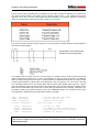
The Assembler instruction:
SWI #3
will encode the value 3 into the unused bits of the SWI instruction. In the SWI ISR routine we can examine the
SWI instruction with the following pseudo code:
switch( *(R14-4) & 0x00FFFFFF)
{
// roll back the address stored in link reg
// by 4 bytes
// Mask off the top 8 bits and switch
// on result
case ( SWI-1)
……
Depending on your compiler, you may need to implement this yourself, or it may be done for you in the compiler
implementation.
© Hitex (UK) Ltd.
Page 24
Chapter 1: The ARM7 CPU
1.10 MAC Unit
In addition to the barrel shifter, the ARM7 has a built-in Multiply Accumulate Unit (MAC). The MAC supports
integer and long integer multiplication. The integer multiplication instructions support multiplication of two 32-bit
registers and place the result in a third 32-bit register (modulo32). A Multiply-Accumulate instruction will take the
same product and add it to a running total. Long integer multiplication allows two 32-bit quantities to be
multiplied together and the 64-bit result is placed in two registers. A long Multiply-Accumulate instruction is also
available.
Mnemonic
Meaning
Resolution
MUL
MULA
UMULL
UMLAL
SMULL
SMLAL
Multiply
Multiply Accumulate
Unsigned Multiply
Unsigned Multiply Accumulate
Signed Multiply
Signed Multiply Accumulate
32-bit
32-bit
64-bit
64-bit
64-bit
64-bit
© Hitex (UK) Ltd.
Page 25
result
result
result
result
result
result
Chapter 1: The ARM7 CPU
1.11 THUMB Instruction Set
Although the ARM7 is a 32-bit processor, it has a second 16-bit instruction set called THUMB. The THUMB
instruction set is really a compressed form of the ARM instruction set.
The THUMB instruction set is
essential for archiving the
necessary code density to
make small single-chip ARM7
micros usable.
This allows instructions to be stored in a 16-bit format, expanded into ARM instructions and then executed.
Although the THUMB instructions will result in lower code performance compared to ARM instructions, they will
achieve a much higher code density. So, in order to build a reasonably-sized application that will fit on a small
single-chip microcontroller, it is vital to compile your code as a mixture of ARM and THUMB functions. This
process is called interworking and is easily supported on all ARM compilers. By compiling code in the THUMB
instruction set you can get a space saving of 30%, while the same code compiled as ARM code will run 40%
faster.
The THUMB instruction set is much more like a traditional microcontroller instruction set. Unlike the ARM
instructions, THUMB instructions are not conditionally executed (except for conditional branches). The data
processing instructions have a two-address format, where the destination register is one of the source registers:
ARM Instruction
THUMB Instruction
ADD R0, R0,R1
ADD R0,R1
R0 = R0+R1
The THUMB instruction set does not have full access to all registers in the register file. All data processing
instructions have access to R0 - R7 (these are called the “low registers”).
Access to R8 - R12 (the “high registers”) on the other hand is restricted to a few instructions:
MOV, ADD, CMP
In the THUMB programmer’s model all
instructions have access to R0 - R7. Only a
few instructions may access R8 - R12.
© Hitex (UK) Ltd.
Page 26
Chapter 1: The ARM7 CPU
The THUMB instruction set does not contain MSR and MRS instructions, so you can only indirectly affect the
CPSR and SPSR. If you need to modify any user bits in the CPSR you must change to ARM Mode. You can
change modes by using the BX and BLX instructions.
NB: When you come out of RESET, or enter an exception mode, you will automatically change to ARM Mode.
After Reset the ARM7 will execute ARM (32-bit)
instructions.
The instruction set can be
exchanged at any time using BX or BLX. If an
exception occurs the execution is automatically
forced to ARM (32- bit)
The THUMB instruction set has the more traditional PUSH and POP instructions for stack manipulation. They
implement a fully descending stack, hardwired to R13.
The THUMB instruction set has dedicated
PUSH and POP instructions which implement
a descending stack using R13 as a stack
pointer.
Finally, the THUMB instruction set contains a SWI instruction which works in the same way as in the ARM
instruction set, but it only contains 8 unused bits, to give a maximum of 255 SWI calls.
© Hitex (UK) Ltd.
Page 27
Chapter 1: The ARM7 CPU
1.12 Summary
By the end of this chapter you should have a basic understanding of the ARM7 CPU. Please see the
bibliography for a list of books that address the ARM7 in more detail. Also, a copy of the ARM7 user manual is
included on the CD accompanying this book.
© Hitex (UK) Ltd.
Page 28
Chapter 2: Software Development
© Hitex (UK) Ltd.
Page 29
Chapter 2: Software Development
2 Chapter 2: Software Development
2.1 Outline
After Chapter 1 you should have a clear idea of the ARM7 programmer’s model. In this chapter we will look at
how you can develop C code to run on the LPC2300. While there are a large number of commercial compiler
tools, as well as the open source GCC compiler, in this book the tutorial examples are based on the Keil
Microcontroller development kit (MDK-ARM). The MDK-ARM is a comprehensive development environment for
ARM-based microcontrollers. It includes an IDE called uVision, the ARM Real View compiler, a real time
operating system, software simulator with peripheral simulation and a JTAG hardware debugger. An add-on run
time library (RTL-ARM) provides a set of middleware components including a TCP/IP stack, embedded file
system, USB and CAN drivers. Increasingly the MDK-ARM is being supported by third party software products
as we will see later.
HiTOP works with many different compilers. In the case of the ARM architecture, the Keil Real View and GNU
compilers are very popular and are used in the following sections. Although we are concentrating on the
LPC2300 family in this book, the Hitex and Keil ARM tools can be used for any other ARM7-based
microcontroller.
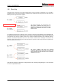
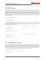
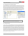
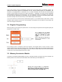
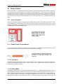
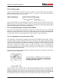
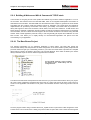
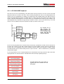
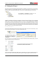
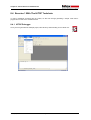
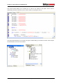
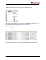
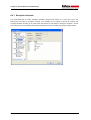
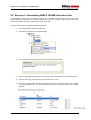
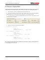
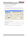
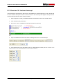
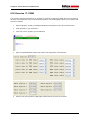
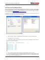
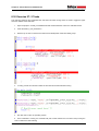
2.1.1 Downloading And Installing The Keil Tools
All of the tutorial exercises in this book are designed to work with the Keil Microcontroller development kit for
ARM (MDK-ARM). If you purchased this book in printed form the evaluation version of Keil MDK-ARM can be
installed from the CD which comes with the book. The MDK-ARM can also be downloaded from
www.keil.com/arm. Even if you have the CD it is worth downloading the development kit to ensure that you have
the latest version. The software will be installed to the following directory structure.
The MDK-ARM installs both the Real View and
legacy CARM compiler. All the current
examples and support files for the Real View
compiler are under the RV30 directory.
Because the legacy CARM compiler is also included with the evaluation MDK-ARM, you need to understand the
structure of the installation to locate the current examples and libraries. In the C:\keil\ARM directory the demo
project in the example and boards directories are for the original CARM compiler and should be ignored. The
Real View compiler examples are in the RV30 in both the boards and examples directories. Although these
examples are not used in this book you should be aware of them as they provide additional material, and Keil
regularly provide new examples with each release of the toolset. Once installed you can start using the MDKARM by starting the uVision IDE.
© Hitex (UK) Ltd.
Page 30
Chapter 2: Software Development
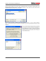
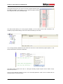
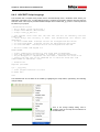
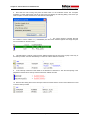
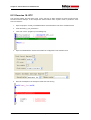
2.1.2 uVision IDE
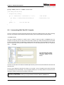
The MDK-ARM consists of the uVision IDE which can be used to host the ARM Real View compiler, the Open
Source GCC compiler or the legacy CARM compiler. The toolset also includes the binary version of the RTLRTOS. This is a real time pre-emptive multitasking operating system designed for use with small footprint ARMbased microcontrollers. uVision also includes two debug tools. Once the code has been compiled and linked it
can be loaded into the uVision simulator. This debugger simulates the ARM7 core and peripherals of the
supported micro. Using the simulator is a very good way of becoming familiar with the LPC2300 devices. Since
the simulator gives cycle accurate simulation of the peripherals as well as the CPU, it can be a very useful tool
for verifying that the chip has been correctly initialised and that the correct values for things such as timer
prescaler values have been correctly calculated.
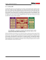
The Keil MDK-ARM is a comprehensive development toolkit specifically designed to support
rapid development of small ARM-based microcontrollers. It integrates IDE, compiler tool chain
debug tools and RTOS with extensive middleware support.
However, the simulator can only take you so far, and sooner or later you will need to take some inputs from the
real world. This can be done to a certain extent with the simulator scripting language, but eventually you will
need to run your code on the real target. The simulator front end can be connected to your hardware by the Keil
ULINK interface. The ULINK interface connects to the PC via USB, and connects to the development hardware
by the LPC2300 JTAG interface. The JTAG interface is a separate peripheral on the ARM7 which supports
debug commands from a host. By using the JTAG you can use the uVision simulator to have basic run control
of the LPC2300 device. The JTAG allows you to download code onto the target, single step and run code at full
speed, set breakpoints and view memory locations.
© Hitex (UK) Ltd.
Page 31
Chapter 2: Software Development
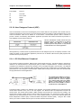
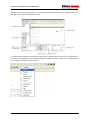
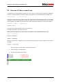
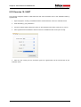
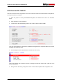
2.1.3 HiTOP IDE
HiTOP supports several different debug tools. You can test generic ARM7 code with the instruction set
simulator, and for standard debugger functions in the real hardware, the Tantino system can be used. Unlike the
Keil ULINK, the Tantino supports ARM9 and ARM11 in addition to ARM7. If you are working with large images,
it also has a shorter download time when programming FLASH, and there are some more sophisticated
debugging functions such as being able to set and clear breakpoints “on-the-fly”.
The HiTOP IDE is an IDE which includes Editor, Project Manager, Make Utility and a
sophisticated debugger. HiTOP is designed to work with most common ARM compilers
including the GCC Compiler and the Real View Compiler.
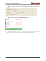
The Tantino is connected via USB to the HiTOP IDE and to the LPC2300 microcontroller through a JTAG
connector. Download, FLASH programming and the basic run control of the LPC2300 device can be performed.
In addition to the JTAG connector, the LPC2300 devices have a second debug port called the “Embedded
Trace Module” (ETM). With this ETM connection, an external Trace tool can record the execution of the
microcontroller, and the trace recording can be displayed in the HiTOP IDE as high-level language lines,
executed instructions or executed cycles. The ETM also allows tracing a data flow within the application. READs
and WRITEs to RAM and SFRs can be recorded in the trace buffer for later analysis. A basic JTAG cannot
access the ETM information, so a more complex system called Tanto is used. The features of this system are
discussed in the Exercises section, but one big advantage is that the Tantino and the Tanto both use the same
HiTOP IDE. A CASE tool called StartEasy is supplied with the Hitex tools that allows you to define an LPC2300
project and generate a project skeleton containing the startup code and initialisation functions for the peripherals
you are going to use. Even if you are not using the Hitex tools, you can download the full version of StartEasy
from the Hitex website.
© Hitex (UK) Ltd.
Page 32
Chapter 2: Software Development
The Tantino is a JTAG debugger with numerous
advanced features including conditional breakpoints for
debugging of ARM instructions, multiple breakpoints in
FLASH memory, “on-the-fly” updates of watch windows
and an exception assistant for trapping run time errors.
2.1.4 The Tutorials
Throughout the remainder of this book there are a number of tutorial exercises that demonstrate a feature of the
software tools or the LPC2300/2400 microcontrollers. The Tutorial section in Chapter 8 talks you through
example programs illustrating the major features of the LPC2300/2400. There are two sets of examples on the
CD, one for the Real View Compiler using the Keil MDK-ARM toolchain and one for the GNU compiler using
the Hitex HiTOP toolchain. Chapter 8 contains introductory tutorial to both development environments. All of the
remaining exercises are held in separate directories which contain the project and a worksheet in a PDF format
that talks you through the exercise so that you can quickly understand the point being made.
The best way to use this book is to read each section then jump to the tutorial and do the exercise. This way, by
the time you have worked through the book you will have a firm grasp of the ARM7, its tools and the LPC2300
/2400 microcontrollers.
Exercise 1: Configuring a New Project
The first exercise covers installing the uVision (Keil tutorial) or installing HiTOP
tutorial) and setting up a first project.
© Hitex (UK) Ltd.
Page 33
(Hitex
Chapter 2: Software Development
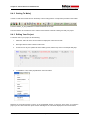
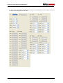
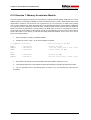
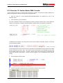
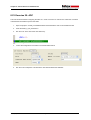
2.2 Interworking ARM/THUMB Code
In our example project we have a number of source files. In practice the .c files are your source code, but the
file “startup.s” is an assembler module provided by Keil. As its name implies, the startup code is located to run
from the reset vector. It provides the exception vector table as well as initialising the stack pointer for the
different operating modes. It also initialises some of the on-chip system peripherals and the on-chip RAM before
it jumps to the main function in your C code. The startup code will vary depending on which ARM7 device you
are using and which compiler you are using, so for your own project it is important to make sure you are using
the correct file. The startup code for the Real View compiler may be found in c:\keil\ARM\RV30\startup\NXP,
and for the GNU use the files in c:\keil\GNU\startup.
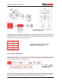
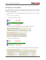
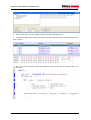
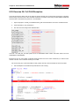
First of all the startup code provides the exception vector table, as shown below. The vector table is located at
0x00000000 and provides a jump to Interrupt Service Routines (ISR) on each vector. To ensure that the full
address range of the processor is available, the LDR (Load Register) instruction is used.
The AREA command is used by the linker to place the vector table at the correct start address. For single chip
use this is always 0x00000000, however if you are using the external bus and want to boot from external
memory, the vector table must be located at 0x80000000. This is explained in Chapter 3. The vector table uses
a Load Register instruction to load a 32-bit constant into the program counter from a constants table that is held
immediately below the vector table. Consequently the vector table requires the first 64 bytes of memory. It is
possible to use a branch instruction in place of the LDR instruction. However, the branch instruction only has an
address range of +- MB. The LDR format can jump the program counter anywhere in the 4 GB address range of
the ARM7. You should also note that the unused vector at 0x00000014 is padded with a NOP. In the NXP
© Hitex (UK) Ltd.
Page 34
Chapter 2: Software Development
LPC2300 these four bytes are used for a special purpose which is discussed in Chapter 3. Finally, the IRQ
vector has a different form of interrupt handling which is also discussed in Chapter 3.
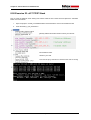
Since each operating mode has a unique R13, there are effectively six stacks in the ARM7. After reset the
startup code must initialise in turn before your application code can start. The strategy used by the compiler is to
locate user variables from the start of the on-chip RAM and grow upwards. Any heap space is then allocated
and then the stack space is allocated.
By default the Real View compiler allocates local variables to CPU registers where possible. The
remaining application data is allocated from the start of the on-chip RAM, followed by any heap data.
Lastly the stack pointers are initialised above the heap. Each stack is assigned a user-allocated
number of bytes.
The startup code enters each different mode of the ARM7 and loads each R13 with the starting address of the
stack:
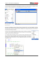
Like the vector table, you are responsible for configuring the stack. This can be done by editing the startup code
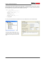
directly; however Keil provide a graphical editor that allows you to configure the stack spaces more easily.
© Hitex (UK) Ltd.
Page 35
Chapter 2: Software Development
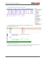
In addition, the graphical editor allows you to configure some of the LPC2300 system peripherals. We will see
these in more detail later, but remember that they can be configured directly in the startup code.
Exercise 2: Startup Code
The second exercise in the Keil or Hitex tutorial takes you through allocating space for each
processor stack, and examines the vector table.
© Hitex (UK) Ltd.
Page 36
Chapter 2: Software Development
2.2.1 Defining The Project Memory Map
When you create a project in the Keil uVision IDE, the “project make” and “linker” files are automatically defined
for the device you are using. In the case of a single-chip device, the FLASH and RAM areas are defined as the
default code and data areas.
You can use the same target dialog to define additional areas of code and data storage if you are using the
external bus to access additional FLASH and RAM. Later on in this chapter, we will look at locating specific
functions and data into these segments.
2.2.2 Defining The Memory Map With The GCC Compiler
Once you have written your source code and compiled it to object files, these files must be linked together to
make the final absolute file. In this section, I would like to give an overview of the GCC linker files that must be
used to build an executable image for the LPC2300/LPC2400. The linker is invoked with the following switches:
ld ld_opt -o <project_name>.elf
where ld_opt is:
-T.\objects\<linker_file>.ld
Map=<project_name>.map
--cref
-t
-static
-lgcc
-lc
-lm
-nostartfiles
-
The linker script file is saved to your project directory and is given the extension .ld. It is important to understand
the structure of this file as you may need to modify it as your application code grows. The linker script file is a
structured text file, with a number of sections that describe your project to the linker. First some search paths
are defined for the compiler libraries. These search paths are defined in HiTOP and must point to the libraries of
the GCC installation you are using:
SEARCH_DIR( "C:\Program Files\Hitex\GnuToolPackageARM\ARM-hitex-elf\lib\interwork"
)
SEARCH_DIR(
"C:\Program
Files\Hitex\GnuToolPackageARM\lib\gcc\ARM-hitexelf\4.0.0\interwork" )
The GCC compiler comes with several builds of the libraries. The version selected here supports ARM/THUMB
interworking. The next section in the script file defines the list of input object files that make up the complete
project:
GROUP ( objects\startup.o
objects\main.o
objects\interrupt.o
objects\THUMB.o )
If you add any additional source modules to your project you must update this list manually.
Following the group section is the target memory layout:
© Hitex (UK) Ltd.
Page 37
Chapter 2: Software Development
MEMORY
{
IntCodeRAM
IntDataRAM
(rx) : ORIGIN = 0x00000000, LENGTH = 512K
(rw) : ORIGIN = 0x40000000, LENGTH = 64k
/* this is flash */
}
This section defines the size and location of the target memory. The description above describes the memory
configuration of the LPC2300/LPC2400 used as a single-chip device with 512k of FLASH memory starting from
address 0x0000000 and 64k of RAM starting from 0x40000000. Later on, when we look at the external memory
interface of the LPC2300/LPC2400, we will look at laying out code for targets with external memory. The final
user section describes how the application code should be laid out within the target memory.
SECTIONS
{
.text
{
…
}
.data
{
…
}
}
The description of the application code is split into two basic sections: “.text” and “.data”. The “.text” section
contains the executable code and the code constants (basically anything that should be located in the FLASH
memory). The “.data” section allocates all of your volatile variables into the user RAM.
.text :
{
__code_start__ = .;
objects\startup.o (.text)
objects\*.o
(.text)
. = ALIGN(4);
__code_end__ = .;
*(.glue_7t) *(.glue_7)
/* Startup code */
} >IntCodeRAM = 0
© Hitex (UK) Ltd.
Page 38
Chapter 2: Software Development
The text section ensures that the startup code is assigned first, so it will be placed on the reset vector. Then the
remaining application code is assigned locations within the FLASH memory. The align command ensures that
each relocatable section is placed on the next available word boundary.
.data : AT (_etext)
{
/* used for initialized data */
__data_start__ = . ;
PROVIDE (__data_start__ = .) ;
*(.data)
SORT(CONSTRUCTORS)
__data_end__ = . ;
PROVIDE (__data_end__ = .) ;
} >IntDataRAM
. = ALIGN(4);
The “.data” section allocates the user variables into the on-chip RAM defined for the LPC2300/LPC2400.
The HiTOP project settings allow you to
customise the IDE for the ARM compiler
you are using and integrate it with the make
utility.
© Hitex (UK) Ltd.
Page 39
Chapter 2: Software Development
2.3 Interworking ARM/THUMB Code
One of the most important things that we need to do in our application code is to interwork the ARM and
THUMB instruction sets. In order to allow this interoperability, ARM have defined a standard called the ARM
Procedure Call Standard (APCS) which is in turn part of the ARM binary standard. The APCS defines, among
other things, how functions call one another, how parameters are passed and how stacks are handled. The
APCS adds a veneer of assembler code to support various compiler features. The more you use, the larger
these veneers get. In theory, the APCS allows code built in different toolsets to work together, so that you can
take a library compiled by a different compiler and use it with the Keil or GCC toolset.
The ARM Procedure Call Standard defines how
the User CPU registers should be used by
compilers. Adhering to this standard allows
interworking between different manufacturers’
tools.
The APCS splits the register file into a number of regions. R0 - R3 are used for parameter passing between
functions. If you need to pass more than 16 bytes, spilled parameters are passed via the stack. Local variables
are allocated to R4 - R11, and R12 is reserved as a memory location for the intra-call veneer code. uVision
allows you a great deal of control over which instruction set is used on each region of your code. At the project
level, in the Options for Target Compiler tab you can globally enable ARM/THUMB interworking and select the
default instruction set.
The same menu is available on each source group folder and for each C module. This allows you to select the ARM or
THUMB instruction set for a group of modules or for individual C modules.
In addition, the programmer can force a given function to be compiled as ARM or THUMB code. This is done
with the two programming directives #pragma ARM and #pragma THUMB, as shown below. The main function
is compiled as ARM code and calls a function called “thumb_function”. (No prizes for guessing that this function
is compiled in the 16-bit instruction set).
#pragma ARM
// Switch to ARM instructions
int main(void)
{
while(1)
{
thumb_function();
}
//Call THUMB function
}
© Hitex (UK) Ltd.
Page 40
Chapter 2: Software Development
#pragma THUMB //Switch to THUMB instructions
void thumb_function(void)
{
unsigned long i,delay;
for (i = 0x00010000;i < 0x01000000 ;i = i<<1)
{
for (delay = 0;delay<0x000100000;delay++)
{
;
}
IOSET1 = i;
//Set the next LED
}
//LED flasher
//simple delay loop
}
2.3.1 Interworking With The GCC Compiler
The GCC compiler also supports interworking between the ARM and THUMB instruction sets. When generating
the code, the compiler must be enabled to allow interworking. This is achieved with the following switch:
-mTHUMB-interwork
The GCC compiler is designed to compile a given C module in either the ARM or THUMBinstruction set.
Therefore you must lay out your source code so that each module only contains functions that will be encoded
as ARM or THUMB functions. By default the compiler will encode all source code in the ARM instruction set. To
force a module to be encoded in the THUMB instruction set, use the following directive when you compile the
code:
-mTHUMB
The HiTOP IDE project settings
allow you to easily define the
compilation settings for each
module.
The linker can then take both ARM and THUMB object files and produce a final executable that interworks both
instruction sets.
Once you have defined the instruction set usage for your project, it can be compiled and the linker will resolve
the interworking issues automatically. As your program develops you can easily reselect an instruction set for
the project, module or function and re-compile, it’s that easy.
Exercise 3: Interworking
This exercise demonstrates setting up a project which interworks ARM and THUMB code.
© Hitex (UK) Ltd.
Page 41
Chapter 2: Software Development
2.4 STDIO Libraries
In the first few chapters of this book we will be writing code that is designed to run without the aid of an
operating system. In this case there is no support for stdin or stdout. In order to use any of the high-level
formatted IO library functions, we must provide low-level drivers tailored to IO devices that we plan to use. The
low-level functions that the Real View libraries call are collected together in a single file called “retarget.c”. The
template of this file can be found in c:\keil\arm\startup\. “Retarget.c” contains two functions that are used by
high-level library calls link “printf” and “scanf”. These functions are used to read and write a single character to
“stdin” and “stdout”.
int fputc(int ch, FILE *f) {
return (sendchar(ch));
}
int fgetc(FILE *f) {
return (sendchar(getkey()));
You need to provide the low-level functions “sendchar” and “getkey” which read and write a single character to
the IO stream. The default functions provided use UART1, but you can adapt these to use a device such as a
memory mapped LCD and keyboard.
int sendchar (int ch)
{
/* Write character to Serial Port
if (ch == '\n') {
while (!(U1LSR & 0x20));
U1THR = CR;
}
while (!(U1LSR & 0x20));
return (U1THR = ch);
*/
/* output CR */
}
int getkey (void)
{
/* Read character from Serial Port
*/
while (!(U1LSR & 0x01));
return (U1RBR);
}
2.4.1 STDIO With The GCC Compiler
The GCC compiler libraries are designed to operate with an operating system designed to the POSIX standard.
This means that the low-level calls of the STRIO libraries make calls to standard functions expected to be
supplied by the operating system. As we are writing procedural C code without an operating system, these
functions must be supplied by our code. The high-level library functions that output data call a low-level function
called “write”, which must be modified to write a single character to the stdout device:
int write (int file, char * ptr, int len) {
int i;
for (i = 0; i < len; i++) putchar (*ptr++);
return len;
}
© Hitex (UK) Ltd.
Page 42
Chapter 2: Software Development
Similarly, the functions such as “scanf” which read data from the stdin device make a low-level call to a function
called “read” to read a single input character:
int read(int file, char *ptr, int len);
{
int i;
for (i=0;i<len;i++) *ptr++ = getchar();
return len;
}
2.5 Accessing Peripherals
Once we have built some code and got it running on an LPC2300 device, it will at some point be necessary to
access the Special Function Registers (SFR) in the peripherals. As all the peripherals are memory mapped they
can be accessed as normal memory locations. Each SFR location can be accessed by ‘hardwiring’ a volatile
pointer to its memory location as shown below.
#define SFR
(*((volatile unsigned long *) 0xFFFFF000))
The Real View Compiler comes with a set of “include” files which define all the SFRs in the different LPC2300
variants. Just include the correct file and you can directly access the peripheral SFRs from your C code. The
names of the “include” files are:
LPC21xx.h
LPC22xx.h
LPC210x.h
2.5.1 Accessing Peripherals With The GCC Compiler
The pointer method used to make absolute access to the Special Function Registers is ANSI C. Consequently
the same “include” file can be used with the GCC Compiler.
© Hitex (UK) Ltd.
Page 43
Chapter 2: Software Development
2.6 Interrupt Service Routines
In addition to accessing the on-chip peripherals, your C code will have to service interrupt requests. It is
possible to convert a standard function into an ISR, as shown below:
void
FIQint (void) __irq
{
IOSET1 = 0x00FF0000;
EXTINT = 0x00000002;
//Set the LED pins
//Clear the peripheral interrupt flag
}
The keyword “__irq” defines the function as either fast or general purpose interrupt request service routine, and
will use the correct return mechanism. Handling software interrupts is a special case and we will look at this in
the next section.
As well as declaring a C function as an interrupt routine, you must link the interrupt vector to the function. We
saw that the interrupt vector table loads a constant (which is the address) on an exception trap loop held in the
startup code. So if you just enable an exception without modifying the startup code, the program will always
end up in the exception trap and never reach your C code. Therefore once we have declared a function as an
interrupt, we must link the vector table to this function as shown below.
Since the ARM CPU will automatically switch to the ARM instruction set when it starts to process an exception,
you must make sure all exception and interrupt routines are coded in the ARM instruction set. The SWI and IRQ
exceptions are special cases. We will look at SWI handling next, and the IRQ interrupt structure in Chapter 3.
© Hitex (UK) Ltd.
Page 44
Chapter 2: Software Development
2.6.1 Interrupt Handling With The GCC Compiler
The principles of handling an exception with the GCC compiler are essentially the same as the Keil Real View
compiler. In the GCC compiler a C routine may be converted into an exception handler by using the non-ANSI
attribute keyword.
void fiqint (void)
{
IOSET1
EXTINT
__attribute__ ((interrupt("FIQ")));
= 0x00FF0000; //Set the LED pins
= 0x00000002;
//Clear the peripheral interrupt flag
}
The keyword “__fiq” defines the function as a fast interrupt request service routine and will use the correct return
mechanism. Other types of interrupt are supported by the keywords “__IRQ”, “__SWI” and “_UNDEF”.
As well as declaring a C function as an interrupt routine, you must link the interrupt vector to the function.
Vectors:
;
Reset_Addr:
Undef_Addr:
SWI_Addr:
PAbt_Addr:
DAbt_Addr:
IRQ_Addr:
FIQ_Addr:
LDR
LDR
LDR
LDR
LDR
NOP
LDR
LDR
LDR
PC,Reset_Addr
PC,Undef_Addr
PC,SWI_Addr
PC,PAbt_Addr
PC,DAbt_Addr
DD
DD
DD
DD
DD
DD
DD
DD
Reset_Handler
Undef_Handler?A
SWI_Handler?A
PAbt_Handler?A
DAbt_Handler?A
0
IRQ_Handler?A
FIQ_Handler?A
/* Reserved Vector */
PC,IRQ_Addr
PC,[PC, #-0x0404]
PC,FIQ_Addr
/* Vector from VicVectAddr */
/* Reserved Address */
The vector table is in two parts. First there is the physical vector table which has a Load Register Instruction
(LDR) on each vector. This loads the contents of a 32-bit wide memory location into the PC, forcing a jump to
any location within the processor’s address space. These values are held in the second half of the vector table,
or constants table which follows immediately after the vector table. This means that the complete vector table
takes the first 64 bytes of memory. The startup code contains predefined names for the Interrupt Service
Routines (ISR). You can link your ISR functions to each interrupt vector by using the same name as your C
function name. The table below shows the constants table symbols and the corresponding C function prototypes
that should be used.
Exception Source
Constant
C Function Prototype
Undefined Instruction
Undef_Handler voidUndef_Handler(void) __attribute__ ((interrupt("undef”)));
Software Interrupt SWI_Handler
void SWI_Handler(void) __attribute__ ((interrupt("swi”)));
Prefetch Abort
PAbt_Handler
void PAbt_Handler (void) __attribute__ ((interrupt("undef”)));
Data Abort
DAbt_Handler
void DAbt_Handler (void) __attribute__ ((interrupt("undef”)));
Fast Interrupt
FIQ_Handler
void FIQ_Handler (void) __attribute__ ((interrupt("fiq”)));
As you can see from the table, there is no routine defined for the IRQ interrupt source. The IRQ exceptions are
special cases as we will see later. Only the IRQ and FIQ interrupt sources can be disabled. The protection
exceptions (Undefined Instruction, Prefetch Abort, and Data Abort) are always enabled. Consequently these
exceptions must always be trapped. As a minimum you should ensure that these interrupt sources are trapped
in a tight loop, as shown below.
Pabt_Handler:
© Hitex (UK) Ltd.
B
Pabt Handler
Page 45
;
Branch back to Pabt_Handler
Chapter 2: Software Development
2.6.2 Debugging The Error Exception Handlers
Three of the ARM exceptions are intended to trap program errors. An Undefined Instruction occurs if the Op
code fetched from the memory is not an ARM or THUMB instruction. Program Abort and Data Abort are
triggered if a fetch or data access is made to a region of memory that is not defined as RAM or ROM or an SFR
region. If one of these protection mechanisms is triggered, your code will end up in the exception traps. If (or
when) this occurs it can be very difficult to work out the cause of the program error without a real time trace.
If your code does encounter a memory error and ends up in one of these loops, you can examine the contents
of the Abort Link Register to determine the address+4 of the instruction which caused the error. The SPSR will
contain details of the operating mode which the CPU was in when the error occurred. From here you can
backtrack and examine the contents of the stack immediately before the application program crashed. So the
CPU registers can produce some useful post mortem diagnostics if you know what you are looking for.
In the HiTOP debugger the
exception assistant allows you to
track back to the last instruction
executed before an exception was
generated.
Exercise 4: Simple Interrupt
This exercise demonstrates how to set up and service a basic FIQ interrupt.
2.6.3 Software Interrupt
As we saw in Chapter 1, the ARM and THUMB instruction sets include a software interrupt instruction. When
executed, the SWI instruction will generate an exception and force the CPU into Supervisor Mode, jumping the
Program Counter to the Software Interrupt Exception Vector. Once in the privileged Supervisor Mode, the CPU
has full access to the CPSR and SPSR registers that are not accessible in User Mode. It also means that code
called by a software interrupt will have its own stack, and if necessary, a dedicated region of memory. This
allows the possibility of partitioning your code into separate operating modes. For example, application code
running in User Mode that makes calls to low-level drivers via software interrupts running in Supervisor Mode.
The low-level drivers can have their own stack and memory region, which cannot be crashed by the application
code. This splits your code into a BIOS layer and an application layer, where each layer can be developed
separately. They can then be linked together with minimal integration problems. The SWI mechanism is also a
useful mechanism for linking together two separately compiled programs, such as an application program and a
bootloader. Dealing with the Software Interrupt Exception is a special case. As we have seen, it is possible to
encode an integer into the unused portion of the SWI opcode.
#define SWIcall2
© Hitex (UK) Ltd.
asm{ swi#2}
Page 46
Chapter 2: Software Development
Now when you enter the Software Interrupt Handler, the return address will be stored in R14, the Link Register.
With some assembler code you can read this value and calculate the address of the SWI instruction that
generated the interrupt. It is then possible to read this memory location mask from the instruction op code to
obtain the integer value. This value can then be used to determine what code should be run in the Software
Interrupt Handler.
However in the Real View Compiler there is a more elegant method of handling software interrupts. A function
can be defined as a software interrupt by using the following non-ANSI keyword adjacent to the function
prototype:
void __swi(1) SysCall_1 (int pattern);
void __SWI_1 (void)
{
………………
}
// void call to software interrupt
In addition, the assembler file SWI.S must be included as part of the project.
Now when a call is made to the function, an SWI instruction is used. This causes the processor to enter the
Supervisor Privileged Mode and execute the code in the SWI_VEC.S file. This code determines which function
has been called and handles the necessary parameter passing. This mechanism makes it very easy to take
advantage of the exception structure of the ARM7 processor, and to partition code which is non-critical code
running in User Mode or privileged code such as a BIOS or Operating System. In the Tutorial section we will
take a closer look at how this works.
2.6.4 Software Interrupts In The GCC Compiler
In the GCC compiler there is no direct support for the software interrupt mechanism. However it is possible to
create a software interrupt call by using the inline assembler. The SWI instruction can also be compiled with a
user-defined integer encoded into the ‘empty’ portion of the instruction (bits 0 - 23), as shown below.
#define SoftwareInterrupt2 asm ("swi #02")
Now when we execute this line of code, it will generate a software interrupt, switch the CPU into Supervisor
Mode and vector the PC to the SWI interrupt vector, which will place the application into the SWI handler
routine. Once we enter this routine, we need to determine what code to run. It would be possible to read the
contents of a global variable, and then use a switch statement to run a specific function depending on the
contents of the global. However, there is a more elegant method. In the GCC compiler there is a register
keyword that allows us to access a CPU register directly from C code. The declaration below declares a pointer
to the Link Register.
register unsigned * link_ptr asm ("r14");
When we enter the Software Interrupt Routine we can use this pointer to read the contents of the SWI
instruction which generated the interrupt. This allows us to read the integer number encoded into the SWI
instruction. We can then use this number to decide which function to run within the SWI handler.
© Hitex (UK) Ltd.
Page 47
Chapter 2: Software Development
temp = *(link_ptr-1) & 0x00FFFFFF;
The line above takes the contents of the Link Register and deducts one. Remember it is a word-wide pointer, so
we are in fact deducting four bytes. This rolls the contents of the Link Register back by four so it is pointing at
the address of the SWI instruction. Then the contents of the instruction with the top eight bits masked off (the
condition codes and the SWI op code) are copied into the temp variable.
The result is that the encoded integer (in this case 2) is now stored in the temp variable and we can use its
contents to decide which code to run. The SWI instruction is a convenient method of leaving User Mode to enter
the Supervisor Mode and run some privileged code. The SWI calls can be used as part of a BIOS where all
access to the special function registers is made via software interrupt calls. This in effect partitions your
application code, so that all the hardware drivers run in Supervisor Mode with their own stack and if necessary
their own memory space. You do not have to build your code this way, but if you want to make use of it the
mechanism is there.
Exercise 5: Software Interrupt
The SWI support in the Keil compiler is demonstrated in this example. You can easily partition code
to run in either the user mode or in supervisor mode.
2.6.5 Locating Variables At Absolute Memory Locations
Please note that the features described in this section and the “Locate Code in RAM” section describe
features that are disabled in the evaluation version of the compiler.
It is often necessary to locate program variables at absolute locations in the LPC2300 memory map. Within a C
module it is possible to locate various program segments at any memory location. This is done by selecting the
required C module within uVision and opening its Options menu. This menu allows you to assign the program
segments within this module to any regions defined in the project target settings.
If you want to locate a variable at a specific location, for example a structure to be located over the memory
mapped registers of an external peripheral, you must define the memory region in the project target dialog.
Then create a “dummy” module that contains only the structure definition, and then locate the “Zero Initialised
Data” (which is in the “dummy” module) into this segment.
2.6.6 Locating Code In RAM
As we shall see later, the main performance bottleneck for the ARM7 CPU is fetching the instructions to execute
from the FLASH memory. The LPC2300 has special hardware to solve this problem for the on-chip FLASH.
However, if you are running from external FLASH, you are stuck with the access time of the external FLASH.
One trick is to boot the executable code into fast RAM and then run from this RAM. This means that you need to
compile position independent code that can be copied into the RAM, or compile code so it runs in the RAM and
is loaded by a separate bootloader program. Both of these solutions will work but require extra effort to develop.
© Hitex (UK) Ltd.
Page 48
Chapter 2: Software Development
Fortunately, the uVision IDE allows you to easily boot code from the FLASH into the RAM. This is done by
simply locating the Code/Const section of a module (or group of modules) into a RAM segment.
Now the selected code will be linked to run from the RAM region, and the default startup code will automatically
load the code from FLASH memory into RAM at runtime. The compiler does not check if your RAM function is
calling functions or library functions that are not also stored in the RAM. So if your “fast” RAM function makes
calls to a maths routine stored in the FLASH memory, you may not get the performance you were expecting.
This method of locating functions in RAM is not only simple and easy to use, it has the added advantage that
the linker knows where the function will finally end up and can place the debug symbols at the correct address.
This will give you not only a ROMable image which will run standalone, but also an image which can be
debugged.
2.6.7 Using The GCC Compiler To Load Code And Data Into RAM
The GCC Compiler has no direct support for locating objects at specific locations, and there are probably a
number of ways to do it. The method discussed here can be used to boot code into RAM and also locate
variables at absolute locations. The basis of the method presented here is the GNU-C “SECTION __attribute__”
directive. This allows a particular object (code or data) to be placed into a section with a user-defined name.
This special section is then fixed in memory at the desired storage address, but has its runtime address set to
somewhere in SRAM via the linker control file.
Step-by-step, the process is:
(i) Define a macro such as:
#define RAMCODE __attribute__ ((section (".ramcode")))
The name “RAMCODE” was chosen as it is distinctive and meaningful, if rather dull.
(ii) Place the RAMCODE macro at the end of the prototype for the function you want to store in ROM but
execute in RAM:
// Erase FLASH Function
// Function prototype sets the attribute
unsigned int erase_flash (unsigned int sector) _RAMCODE_ ;
Note: The function itself is not changed. The presence of the RAMCODE macro and hence the
“__attribute__(section())” control will cause the code generated for the function to be placed into a SECTION
called “.ramcode”.
© Hitex (UK) Ltd.
Page 49
Chapter 2: Software Development
(iii) Add the lines after “PROVIDE (etext = .);” to the .LD linker control file:
/* .rodata section which is used for read-only data (constants) */
.rodata . :
{
*(.rodata)
} >IntCodeRAM
. = ALIGN(4);
/* Create a symbol that can be accessed from C */
_ramcode_rom_image = . ;
PROVIDE (ramcode_rom_image = .) ;
_etext = . ;
PROVIDE (etext = .);
/* ADD THE FOLLOWING LINES */
/********************************************/
/* Code that will be stored in ROM and */
/* copied to RAM in main() */
/* It is placed in the IntDataRAM (SRAM), */
/* defined in the MEMORY { } section at the */
/* at the top of this file */
/* The .ramcode section comes from RAMCODE.C */
/* Please send your donations to Mike Beach */
.ramcode :
/*
AT
{
/*
/*
Put the ROM image at the end of the .rodata area */
( ADDR (.rodata) + SIZEOF (.rodata))
Set the values of the public symbols called */
_ramcode and _eramcode that will be accessed from C */
_ramcode = . ; *(.ramcode) ; _eramcode = . ;
} >IntDataRAM
/* Create the _eramcode symbol */
PROVIDE (_eramcode = .);
Here, the function will be stored in ROM after the “.rodata” section. Generally this is at the top of the used
Code/Constant area.
© Hitex (UK) Ltd.
Page 50
Chapter 2: Software Development
These lines create public symbols called “_eramcode” (end of ramcode) and “_ramcode” (start of ramcode),
which are used by the copy routine to determine the destination address. The “ramcode_rom_image” symbol is
used to find the stored function in the ROM. These are referenced in C modules using:
extern unsigned long _eramcode ; // End of area in RAM
extern unsigned long _ramcode ; // Start of area in RAM at which functions
// will be loaded
extern unsigned long _ramcode_rom_image ; // Start of area in ROM in which
// functions are stored
(iv) Add the following code to the start of your main() function. This copies the function from ROM to RAM, ready
for execution:
// Copy FLASH Erase and Write Functions Into SRAM
// Point to base of ROM image of functions
func_copy_ptr = (unsigned long *) &_ramcode_rom_image ;
// Point to final run time address of functions
ramcode_ptr = (unsigned long *) &_ramcode ;
// Find length of area to copy from ROM to RAM
func_copy_length = (unsigned long) &_eramcode - (unsigned long) &_ramcode ;
// Do the copy
for(i = 0 ; i < func_copy_length/sizeof(unsigned int) ; i++)
{
ramcode_ptr[i] = func_copy_ptr[i] ;
}
You will need to have some suitable pointers already defined:
unsigned long *func_copy_ptr ;
unsigned long *ramcode_ptr ;
unsigned long func_copy_length ;
(v) Due to the great distance between the ROM from where the function will be called (0x00000000) and the
execution address in RAM (0xA0000000), it is not possible to make a direct function call to run the function.
Instead you need to use a function point and use an indirect call:
// Get start addresses of functions now located in SRAM
// We cannot call functions at 0xA0000000 directly so we need to use
// function pointers
SRAM_erase_FLASH_func = (unsigned long (*)(unsigned int))&erase_flash ;
SRAM_write_FLASH_func = (unsigned long (*)(unsigned int,
unsigned int))&write_flash ;
To call the function in RAM, use:
// We are in BANK0
// ERASE sector 4 at 0x8000
error_status = SRAM_erase_FLASH_func(0x10) ; // Function located in SRAM
© Hitex (UK) Ltd.
Page 51
Chapter 2: Software Development
(vi) Look in the MAP file and check that the .ramcode section is in the right place and that the ROM image of the
function is just after the .rodata section:
.rodata 0x00000618 0x0
*(.rodata)
0x00000618 . = ALIGN (0x4)
0x00000618 _ramcode_rom_image = .
0x00000618 PROVIDE (ramcode_rom_image, .)
0x00000618 _etext = .
0x00000618 PROVIDE (etext, .)
.ramcode 0xa0000000 0x1dc load address 0x00000618
0xa0000000 _ramcode = .
*(.ramcode)
.ramcode 0xa0000000 0x1dc objects\ramcode.o
0xa0000000 erase_flash
0xa00000ec write_flash
0xa00001dc _eramcode = .
0xa00001dc PROVIDE (_eramcode, .)
And that’s all there is to it!
2.6.8 Debug Information When In RAM
Because the GNU-C compiler and linker are being used properly, you will find that the debug information
required by the HiTOP debugger is fixed up at the execution address, so when you run until the function, the full
source level debugging will be available!
© Hitex (UK) Ltd.
Page 52
Chapter 2: Software Development
2.7 Inline Functions
It is also possible to increase the performance of your code by inlining your functions. The inline keyword can be
applied to any function, as shown below:
__inline void NoSubroutine (void)
{
…
}
When the inline keyword is used, the function will not be coded as a subroutine, but the function code will be
inserted at the point where the function is called, each time it is called. This removes the prologue and epilogue
code which is necessary for a subroutine, making its execution time faster. However, you are duplicating the
function every time it is called, so it is expensive in terms of your FLASH memory.
2.7.1 Inline Functions With The GCC Compiler
The GCC Compiler also supports inlining of C functions in a very similar fashion to the Real View Compiler:
inline void NoSubroutine (void)
{
…
}
When the inline keyword is used, the function will not be coded as a subroutine, but the function code will be
inserted at the point where the function is called, each time it is called. This removes the prologue and epilogue
code which is necessary for a subroutine, making its execution time faster. However, you are duplicating the
function every time it is called, so it is expensive in terms of your FLASH memory. The compiler will not inline
functions unless you have set the optimiser to its “O2” level.
© Hitex (UK) Ltd.
Page 53
Chapter 2: Software Development
2.8 Inline Assembler
The compiler also allows you to use ARM or THUMB Assembler instructions within a C file. This can be done as
shown below:
__asm {
loop:
LDRB
STRB
CMP
BNE
ch, [src], #1
ch, [dst], #1
ch, #0
loop
}
This can be useful if you need to use features which are not supported by the C language, for example the MRS
and MSR instructions.
2.8.1 Inline Assembler With The GCC Compiler
Again, like the Real View Compiler the GCC compiler allows you to add assembler instructions inline with your
C code.
asm ( “mov r15,r2”
);
2.8.2 Importing GCC Code
One interesting feature of the Real View Compiler is that it has a GNU emulation mode. By adding the “–gnu”
switch to the compiler command line, the Real View Compiler can build a project originally written for the GCC
compiler. Since both the Real View Compiler and the GCC Compiler comply to the ARM binary interface
standard, it is possible to build a mixed project composed of code written in both the GCC dialect and the Real
View dialect.
This raises the interesting possibility of compiling existing Open Source code in the leading industry standard
C/C++ compiler.
© Hitex (UK) Ltd.
Page 54
Chapter 2: Software Development
2.9 Hardware Debugging Tools
NXP have designed the LPC2300 to have the maximum on-chip debug support. There are several levels of
support. The simplest is a JTAG debug port. This port allows you to connect to the LPC2300 from the PC for a
debug session. The JTAG interface allows you to have basic run control of the chip. That is, you can single step
lines of code, run halt and set breakpoints and also view variables and memory locations once the code is
halted.
Debug support on the LPC2300 includes a JTAG port for FLASH programming and basic run control
debugging.
In addition, NXP has included the ARM embedded trace module. The embedded trace module provides much
more powerful debugging options and real time trace, code coverage, triggering and performance analysis
toolsets. In addition to more advanced debug tools, the ETM allows extensive code verification and software
testing which is just not possible with a simple JTAG interface. If you are designing for safety-critical
applications, this is a very important consideration.
In addition to the JTAG port, NXP have included the ARM ETM module for high-end debugging tools.
The final on-chip debug feature is the Real Monitor. This is a kernel of code which is resident in a reserved area
of memory. During a debug session the debugger can start the Real Monitor via the JTAG port. The Real
Monitor can be used to provide “on the fly” updates as your code is running. This process is pseudo real time in
that the Real Monitor code interrupts your code and uses some processor time to read and communicate debug
information to the PC.
2.9.1 Important!
The JTAG and ETM tools simply provide a fairly “dumb” serial debug connection to the ARM7 core. A generic
ARM JTAG tool does not have any understanding of the overall LPC2300 architecture. This means that a
generic tool will always enter the bootloader after reset because it does not write the “program signature” into
the FLASH (this feature is discussed later). Consequently, it will never run your code. If you are new to the
© Hitex (UK) Ltd.
Page 55
Chapter 2: Software Development
LPC2300, this is likely to catch you out and be very frustrating. Since the Keil tools are developed for ARM7based general purpose microcontrollers, uVision understands the LPC2300 memory architecture and will debug
the device seamlessly.
2.9.2 Even More Important
As mentioned above, the JTAG port is a simple serial debug connection to the ARM7 device. It is very important
to understand its behaviour during reset. If the ARM7 CPU is reset, all of the peripherals including the JTAG are
reset. When this happens, the ULINK debugger loses control of the chip and has to re-establish control once the
LPC2300 device comes out of reset. This will take a finite number of clock cycles. While this is happening, any
code which is on the chip will be run as normal. Once the ULINK regains control of the chip, it performs a soft
reset by forcing the PC back to address zero. However, the on-chip peripherals are no longer in the reset
condition, i.e. peripherals will be initialised, interrupt enabled etc. You must bear this in mind if the application
you are developing could be adversely affected by this. A quick solution is to place a simple delay loop in the
startup code or at the beginning of main(). After a reset occurs, the CPU will be trapped in this loop until the
ULINK regains control of the chip. None of the application code will have run, leaving the LPC2300 in its
initialised condition.
2.10 Summary
So, by the end of this section you should be able to set up a project in the Keil or Hitex tools, select the compiler
and LPC2300 variant you want to use, configure the startup code, be able to interwork the ARM and THUMB
instruction sets, access the LPC2300 peripherals and write C functions to handle exceptions. With this
grounding, we can now have a look at the LPC2300 system peripherals.
© Hitex (UK) Ltd.
Page 56
Chapter 3: System Peripherals
© Hitex (UK) Ltd.
Page 57
Chapter 3: System Peripherals
3 Chapter 3: System Peripherals
3.1 Outline
Now that we have some familiarity with the ARM7 core and the necessary development tools, we can begin to
look at the LPC2300 devices themselves. In this section we will concentrate on the system peripherals, that is to
say the features which are used to control the performance and functional features of the device. This includes
the on-chip FLASH and SRAM memory, the external bus controller, the clock structure and phase locked loop
which is used to multiply the external oscillator in order to provide a maximum of 72MHz processor clock, and
the power control features. Finally, we will take a look at the simplest user interrupt source, the external interrupt
pins, before going on to look at the exception system in detail.
3.2 Bus Structure
To the programmer, the memory of the LPC2300 device is one contiguous 32-bit address range. However, the
device itself is made up of a number of buses. These buses are defined by ARM and in general an ARM-based
microcontroller contains two buses. The ARM7 core is connected to a high-speed bus called the Advanced High
Performance Bus (AHB). As its name implies, this is the fastest way of connecting peripheral devices to the
ARM7 core, and is generally reserved for high performance peripherals such as the Vector Interrupt Controller
which enables fast interrupt handling, and USB and Ethernet controllers.
All the remaining user peripherals are connected to a second standard bus called the Advanced Peripheral Bus.
The APB bridge contains a clock divider, this allows the APB bus to run at a slower speed than the ARM7 core
and the AHB. This allows the user peripherals to run at a slower clock rate than the main processor to conserve
power. The general form of an ARM7-based microcontroller is shown below.
The generalised bus structure of an
ARM7 based microcontroller consists
of a single AHB bus and a single APB
bus.
The LPC2300 has been designed with several high performance peripherals, each with their own DMA units.
These require frequent bus access, and the basic bus structure would limit overall performance of the
microcontroller because the ARM7 and DMA units would be continually arbitrating with one another. For this
reason the LPC2300 has a more complex bus structure which consists of two AHB buses, a single APB bus and
an additional local bus interface to the ARM7 CPU.
© Hitex (UK) Ltd.
Page 58
Chapter 3: System Peripherals
The LPC2300 introduces a second
AHB bus dedicated to the Ethernet
peripheral, and a local bus for the
FLASH and SRAM.
The Ethernet MAC and DMA has its own dedicated high speed AHB bus. The USB controller and its dedicated
DMA is located on the second AHB bus along with the general purpose DMA unit. All of the general purpose
peripherals are bridged off this AHB bus onto a single APB bus.
Finally, there is a third local bus which is used to connect the on-chip FLASH and RAM to the CPU. Connection
of the program code and data store to the ARM7 CPU via the AHB bus is possible, but this introduces some
execution stalls because of contention on the bus. Using a separate local bus removes the possibility of these
stalls to give the best processor performance. Because it is so much faster to read and write to registers on the
local bus, NXP have moved the GPIO registers onto the local bus. As we will see later this allows you to “bit
bash” port pins much faster than using registers located on the APB bus.
3.3 Memory Map
Despite the number of internal buses, the LPC2300 has a completely linear memory map. The general layout is
shown below.
The memory map of the LPC2300 includes
regions for on-chip FLASH memory, user
SRAM, a pre-programmed bootloader, external
bus and user peripherals.
Fig Memory map
© Hitex (UK) Ltd.
Page 59
Chapter 3: System Peripherals
The on-chip FLASH is fixed at 0x00000000 upwards with the user RAM fixed at 0x4000000 upwards. The
dedicated USB SRAM appears at 0x7FD00000 and the Ethernet SRAM appears at 0x7FE00000. The
LPC2300 is pre-programmed at manufacture with a FLASH bootloader and the ARM real monitor debug
program. These programs are placed in the region 0x7FFFFFF – 0x8000000. The region between 0x8000000
and 0xE000000 is reserved for external memory. The user peripherals located on the AHB are all mapped into
the region between 0xE000000 and 0xE020000, and each peripheral is allocated a 16k memory page. Finally
the Vector Interrupt Unit is located at the top of the address range at 0xFFFFF000.
If your user code tries to access memory outside these regions, or non-existent memory within them, an abort
exception will be produced by the CPU. This mechanism is hardwired into the design of the processor and
cannot be changed or switched off.
3.4 Register Programming
Before we start our tour through the system block, it is worth noting how Special Function Registers (SFR) are
programmed on ARM7 chips.
As a general rule all Special
Function Registers originating from
ARM are controlled by three
registers: a Set, Clear and Status
register.
NB To clear bits you must write a
logic 1 to the relevant bit in the
Clear Register.
Each underlying SFR is controlled by three user registers. A Set register which is used to set bits, a Clear
register which is used to clear bits by writing a logic 1 to the bits you wish to clear, and a Status register which is
used to read the current contents of the register. The most common mistake made when new to the LPC2300 is
to write zero into the Clear Register which has no effect.
3.5 Memory Accelerator Module
The Memory Accelerator Module (MAM) is the key to the high instruction execution rate of the LPC2300. The
MAM is present on the local bus and sits between the FLASH memory and the ARM7 CPU.
Running from on-chip FLASH is a performance
bottleneck for all ARM7 implementations. NXP have
added a Memory Accelerator Module which greatly
enhances the performance of the ARM7 CPU.
© Hitex (UK) Ltd.
Page 60
Chapter 3: System Peripherals
One of the main constraints in designing a high performance, single-chip microcontroller based on the ARM7 is
the access time to the on-chip FLASH memory. The ARM CPU is capable of running up to 80MHz, however the
on-chip FLASH has an access time of 50ns. Consequently, just running out of the FLASH would limit the
execution speed to 20MHz (a quarter of the possible clock rate of the processor.) There are a number of ways
round this problem. The simplest is to load the critical sections of your program into RAM and run out of RAM.
As the RAM has a much faster access time, our overall performance will be greatly increased. The downside is
that on-chip RAM is a finite and precious resource. Using it to hold program instructions greatly limits the size of
application code which we could run. Another approach would be to have an on-chip cache. A cache is a small
region of memory placed between the processor and memory store, which stores regions of recently referenced
main memory. In a well-designed cache, the processor will use the cache memory whenever possible, thus
reducing the bottleneck imposed by slow memory. However, a full cache is a complex peripheral that demands
a high number of gates and consequently a large portion of the LPC2300 die area. This flies in the face of the
ARM7 design, which has simplicity as its watchword. Another downside of a full cache is that the runtime of
code using the cache is no longer deterministic and could not be used by any application that required
predictability and repeatability.
The Memory Accelerator Module is a compromise between the complexity of a full cache and the simplicity of
allowing the processor to directly access the FLASH memory.
The FLASH memory is arranged in a bank of
128-bit wide memory. One FLASH access
from the MAM loads four ARM instructions or
eight THUMB instructions which can be
executed by the ARM7 CPU.
Like a cache, the MAM attempts to have the next ARM instruction in its local memory in time for the CPU to
execute. First of all the FLASH memory is 128 bits wide (four instructions) rather than 32 bits wide. This means
that a single FLASH access can load four ARM instructions or eight THUMB instructions to fast memory located
in the MAM unit. This memory includes prefetch, data and branch trail buffers. This technique works particularly
well with the ARM instructions, which can use the condition codes to iron out small branches in order to keep
the code-flow largely linear. In the case of small loops and jumps, the MAM has branch and trail buffers that
hold recently loaded instructions which can be re-executed if required.
The complexities of the MAM are transparent to the user and it is configured by two registers, the Timing
Register and the Control Register. There are some additional registers to provide runtime information on the
effectiveness of the MAM. The Timing Register is used to control the relationship between the CPU clock and
the FLASH access time. By writing to the first three bits of the Timing Register you can specify the number of
CPU clock cycles required by the MAM to access the FLASH. The recommended settings are 1 for a system
clock slower than 20MHz, 2 for a system clock between 20 MHz - 40 MHz and 3 for a system clock above 40
MHz.
© Hitex (UK) Ltd.
Page 61
Chapter 3: System Peripherals
On reset the MAM is disabled and all access to code and constant data is made directly to the FLASH. It is
possible to partially enable the MAM so that all sequential code is fetched from it, but branches and constant
data stored in the FLASH are accessed directly from the FLASH. Finally, the MAM may be fully enabled so that
it fetches all FLASH memory accesses from the MAM. The reason for these modes is that, like a cache code,
running from the MAM is not deterministic, so we have the option to switch it off or reduce its impact if we need
to guarantee the run time of our application code. However, even in its full operating mode, the impact of the
MAM is not as great as a cache. It is possible to predict runtime performance particularly with the ‘use
performance analysis’ features in development tools.
To help with this analysis and also to gauge the effectiveness of the MAM, there are a group of statistical
registers which can be used to measure the MAM’s performance.
The MAM has some statistics
registers which show the number of
accesses to the FLASH and the
number of accesses to the MAM, so
the effectiveness of the MAM can be
calculated.
The Statistics registers are based around two counters which record the accesses made to the FLASH and the
accesses made to the MAM buffers. The Statistical Control Register can further refine the type of access which
will cause the counters to increment. By configuring the Statistical Control Register we can differentiate between
code constant and instruction fetches, so it is possible to determine the instruction or data hit rate or the
combined instruction and data hit rate. These metrics can give us some information on the efficacy of the MAM
with our application. On the CD there is a simple example which demonstrates the use of the MAM, its statistical
registers and how vital it is to the overall performance of the LPC2300 family.
© Hitex (UK) Ltd.
Page 62
Chapter 3: System Peripherals
3.5.1 Example MAM Configuration
The example code shown below starts the LPC2300 with the PLL set to 60MHz and the MAM disabled. The
code FLASHes each LED in sequence with a delay loop between each increment. An A/D conversion is also
done and if the result is above 0x00000080, the code enables the MAM for maximum execution speed. The
effect of the MAM can be seen on the update rate of the LEDs. In the next section we will look at burning the
code into the FLASH to observe its operation.
int main(void)
{
unsigned int delay;
unsigned int FLASHer = 0x00010000;
IODIR1 = 0x00FF0000;
VPBDIV = 0x02;
ADCR
= 0x00270601;
ADCR |= 0x01000000;
// define locals
// set all ports to output
// Setup A/D: 10-bit AIN0 @ 3MHz
// Start A/D Conversion
while(1)
{
do
{
val = ADDR;
}
// Read A/D Data Register
while ((val & 0x80000000) == 0);
val = ((val >> 6) & 0x03FF);
if (val <0x80)
{
MAMCR = 0;
MAMTIM = 0x03;
MAMCR = 0x02;
}
else
{
MAMCR = 0x0;
}
for(delay = 0;delay<0x100000;delay++) //simple delay loop
{
;
}
ChangeGPIOPinState(FLASHer);
FLASHer = FLASHer <<1;
//set the state of the ports
//shift the active led
if(FLASHer&0x01000000)
{
FLASHer = 0x00010000; //Increment FLASHer led and test for
// overflow
}
}
}
void ChangeGPIOPinState(unsigned int state)
{
IOCLR1 = ~state;
IOSET1 = state;
//clear output pins
//set output pins
}
© Hitex (UK) Ltd.
Page 63
Chapter 3: System Peripherals
3.6 FLASH Memory Programming
Although the internal FLASH is arranged as a 128-bit wide bank, you will be relieved to know that, to the user, it
can be treated as one contiguous memory space and no special tools are required to prepare the code prior to
programming the chip. In terms of programming the FLASH, to the user it appears as a series of 8K sectors
which can be individually erased and programmed. There are several methods which can be used to program
the on-chip FLASH. The easiest is by the built-in bootloader which allows your code to be downloaded via
UART 0 into RAM and then be programmed into the FLASH. It is also possible to use a JTAG development tool
to program the memory. This is useful during development because it can be done from the debugging
environment without the need to keep switching between debugger and bootloader. Also, the JTAG connection
can be very fast, up to 400Kbytes/sec download, so in large applications, particularly those using external
FLASH memory, it can be the best method of production programming. Finally it is also possible to reprogram
sections of the FLASH memory under command of the application already on the chip. This, in application
programming, can use any method to load the new code onto the chip (SPI CAN I2C) and then load it into a
given section of FLASH. So there is an easy to use mechanism which allows field updates to your application.
3.6.1 Memory Map Control
Before looking at the operation of the bootloader we must first understand the different memory modes available
on the LPC2300. As we have seen, the ARM7 interrupt vector table and its constants table take up the first 64
bytes of memory. In the LPC2300 these first 64 bytes may be mapped from a number of locations, depending
on the mode set in the MEMMAP Register. It is important to note that these modes have nothing to do with the
ARM7 operating modes. The MEMMAP Register allows you to select between Boot Mode, FLASH Mode, RAM
Mode and External Memory Mode. When selected, a new vector table will be mapped into the first 64 bytes of
memory. So for the RAM Mode the contents of 0x4000000 - 0x400003F will be mapped to the start of memory.
This allows a program to be loaded into RAM starting at 0x4000000 and the vector table can then be redirected,
thus allowing the program and its interrupts to run in RAM. This mode is normally only used for debugging small
programs. FLASH Mode leaves the first 64 bytes of user FLASH unchanged and is the normal mode for user
applications. Boot Mode replaces the first 64 bytes of FLASH with the vector table for the bootloader and places
a jump to the on-chip bootloader on the reset vector.
The MEMMAP Register maps the first 64 bytes of memory
from one of four regions.
© Hitex (UK) Ltd.
Page 64
Chapter 3: System Peripherals
3.6.2 Bootloader
Every time the LPC2300 comes out of reset its memory map will be in Boot Mode, so the instruction on the
reset vector will cause it to jump into the bootloader code entry point at 0x7FFFFFFF. This can be the bane of
new users if they load their code into FLASH with a JTAG, reset and single step the first instruction, only to find
that the program counter is at some wild high address. If this happens, you need to program the MEMMAP
register to 0x00000002, to force the chip into FLASH mode and return to the user vector table.
Once the bootloader code has been entered, it will perform a number of checks to see if the FLASH needs to be
programmed. First the watchdog is checked to see if the processor has had a hard reset of a soft reset. If it is a
hard reset, the logic level on pin 2.10 will be tested. If it is low, then the bootloader command handler will be
entered. If it is a soft reset (i.e. watchdog timeout) or pin 2.10 is high, then there is no external request to
reprogram the FLASH. However, before handing over to the user application, the bootloader will check to see if
there is a valid user program in FLASH. In order to detect if a valid program is present, every user program must
have a program signature. This signature is a word-wide number that is stored in the unused location in the
ARM7 vector table at 0x00000014. The program signature is the two’s compliment of the checksum of the
ARM7 vector table.
The program signature is calculated as
the two’s compliment of the checksum
of the vector table. This signature must
be stored in the unused vector at
0x00000014 or your program will not run
When this value is summed with the program signature the result will be zero for a valid program. If a valid
program is detected, the memory operating mode is switched to FLASH (which restores the user vector table),
the program counter is forced to zero and the user application starts execution. If there is no valid program, then
the bootloader enters its command handler. So, without the program signature your code will never run! The
program signature can be added to your startup code as shown below:
LDR
LDR
LDR
LDR
LDR
PC,
PC,
PC,
PC,
PC,
Reset_Addr
Undefined_Addr
SWI_Addr
Prefetch_Addr
Abort_Addr
.long
LDR
LDR
0xB8A06F58
PC, IRQ_Addr
PC, FIQ_Addr
/* Program signature */
3.6.3 NXP ISP Utility
If there is a valid program signature, or pin 2.10 is held low after reset, the LPC2000 will start the bootloader.
Before handing over to the command handler it enters an auto-Baud routine. This routine listens on UART 0 for
a synchronisation character. When this is sent by the host, the LPC2000 measures the bit period and adjusts
the UART 0 Baud rate generator to match the host. Once this is done some further handshaking and
configuration takes place and then control is passed to the command handler.
The Bootloader command handler takes commands from UART 0 in ASCII format. The command set is shown
below and allows you full programming control of the FLASH. In addition the GO command is a simple
© Hitex (UK) Ltd.
Page 65
Chapter 3: System Peripherals
debugging command which can be used to start execution of code loaded into RAM. A full description of the
bootloader communication protocol is given in the LPC2000 datasheet.
NXP provide a ready made FLASH In System Programming utility for the PC which can be used to program the
development board. This tool automatically calculates and adds the program signature to your code, to ensure
that your program will run. If you are using this tool to program the FLASH, your code should have a NOP
instruction on the unused vector for the tool to work correctly.
Exercise 11: Memory Accelerator Module and FLASH Programming Utility
This exercise describes the use of the NXP FLASH programming tool to load a simple program into
the LPC2000. This program runs without the MAM switched on. By adjusting the A/D value the MAM
is enabled, so we can see the performance increase caused by this important peripheral.
© Hitex (UK) Ltd.
Page 66
Chapter 3: System Peripherals
3.6.4 In-Application Programming
It is also possible to reprogram the FLASH memory from within your program. All of the bootloader commands
are available as an on-chip API and can be called by your code. To access the bootloader functions you must
set up a table in RAM which contains a command code for the function you want to use followed by its
parameters. The start address of this table is stored in R0. The start address of a second table which contains
the status code and function results is stored in R1.
The bootloader functions can be
accessed to perform in-application
programming. Commands are passed
via two tables in memory. The start
addresses for each table are stored in R0
and R1.
The IAP entry point is at 0x7FFFFFF0 if you wish to call the functions from a THUMB function, or at
0x7FFFFFF1 if you wish to enter from an ARM function. The return address is expected to be stored in the Link
Register. This convention is designed to work within the ARM procedure call standard. A method of calling the
IAP routines through function pointers is detailed in the datasheet. An alternative method is shown below and
both methods are used in the example program. If you are short of program space you can experiment with both
methods to see which is the most efficient in your compiler.
If we define a THUMB function with three parameters as shown below, we can pass the start address of a
command and result array and according to the APCS convention these values will be stored in R0 and R1.
void iap (unsigned *cmd, unsigned *rslt, unsigned entry)
{
asm("mov r15,r2");
}
We can also store the address of the entry point to the IAP routines in the next available parameter register: R2.
In THUMB Mode we cannot program the high registers directly, but we can move low registers to high registers,
hence we can move the contents of R2 directly into the program counter and initiate the requested InApplication Programming routine. When the IAP routine has finished, it will return to your application code using
the value stored in the Link Register, which is the next instruction in the function which called our void IAP (…)
function. You should also note that the In-Application functions return in ARM Mode not THUMB. The IAP
functions require the top 32 bytes of on-chip RAM, so you must either locate the stacks to start below this region
so it is unused, or, if you need all the RAM, place the IRQ stack at the top of memory and disable interrupts
before you enter the IAP routines. Using a pointer, you can now copy the top 32 bytes of on-chip SRAM into a
temporary array and then restore them once you return from the IAP functions. This way you will not risk
corrupting any stacked data.
© Hitex (UK) Ltd.
Page 67
Chapter 3: System Peripherals
3.6.5 FLASH Protection
When your design goes into production it is often necessary “lock” the FLASH Memory so your code cannot be
patched or pirated. To protect your code on the LPC2300 you must locate the word 0x87654321 at location
0x000001FC. When the LPC2300 leaves reset and enters the bootloader this location will be checked, and if
the protection pattern is found the bootloader code will disable the JTAG and disable any commands in the
bootloader command handler which can be used to read or modify the FLASH memory. If you need to do field
firmware updates you can recover access to the FLASH by using the bootloader to erase all the contents of the
FLASH. This clears the protection pattern, and full access to the FLASH is then granted by the bootloader. The
in-application programming routines are still enabled when the FLASH is locked so it is still possible for the
application code to modify the FLASH memory.
© Hitex (UK) Ltd.
Page 68
Chapter 3: System Peripherals
3.6.6 System Clocks
The
internal
clock of the
LPC2300 may
be generated
from one of
three
oscillators
which may be
configured
and selected
dynamically.
The LPC2300 has two main internal clocks. The first is Cclk, the CPU clock, which is used to clock the ARM7
CPU and the AHB peripherals which include the USB controller, Ethernet controller and the general purpose
DMA. The second internal clock is Pclk, the peripheral clock, which is used to clock all the peripherals on the
APB bus. Both of these clocks may be derived from one of three oscillator sources, an internal RC oscillator, an
external main oscillator and an external watch crystal.
The LPC2300 clock system is
controlled by an array of control and
divider registers.
After reset the LPC2300 will default to using the internal RC oscillator. This oscillator has a nominal frequency of
4 MHz. You can run the LPC2300 entirely from this clock source and it may be used as an input to the PLL.
However it is not accurate enough to be used for the USB controller. Only the main external oscillator is stable
enough to provide an accurate clock source for the USB controller. The RC oscillator allows the LPC2300 to
start processing instructions while the main external oscillator is still stabilising. This allows a fast startup after
reset or fast exit from a Power Down Mode. The RC oscillator also provides a known clock frequency for the
bootloader code which will always run after a hard reset. Once the bootloader code has run and the application
code is entered, the system clock source may be selected with the Clock Source Select Register. This register
controls which oscillator is connected to the input of the Phase Locked Loop.
© Hitex (UK) Ltd.
Page 69
Chapter 3: System Peripherals
On exit from reset the LPC2300 will run on the internal RC oscillator and the main oscillator is disabled. The
startup code must first enable the external oscillator by setting the OSCEN bit in the System Control and Status
Register. You must also configure the OSCRANGE bit to select either an external frequency of 1 MHz - 20 MHz
or 15 MHz - 24 MHz.
The System Control and Status
Register must be programmed after
reset to enable the main external
oscillator.
Once the external oscillator is enabled the OSCSTAT bit will be set once it has become stable. When this
happens you can make the external oscillator the main system clock by programming the CLKSRC field in the
Clock Source Select Register. However you must ensure that the PLL is not connected when you switch system
clocks. Care should be taken here as the bootloader code enables the PLL and leaves it connected before
handing over to your application code.
3.6.7 Phase Locked Loop
The LPC2300 PLL is designed to work over a wide range of input frequencies from 32 KHz up to 50 MHz, so it
can work with the on-chip RC oscillator, the RTC oscillator or the main external oscillator. However only the
main external oscillator is capable of generating a frequency stable enough to clock the USB peripheral.
The PLL is used to multiply the
external crystal frequency up to the
maximum 550 MHz to provide an
intermediate frequency which is
divided down to provide the CPU and
peripheral clocks.
© Hitex (UK) Ltd.
Page 70
Chapter 3: System Peripherals
The PLL is used to derive an output frequency which must be in the range 275 MHz - 550 MHz. This PLL
frequency is then divided down to provide separate clocks for the USB controller, USBclk and the CPU Cclk. A
further set of dividers is used to generate the individual Pclk’s clocks for each of the peripherals on the APB bus.
The output from
the PLL enters a
series of dividers
that are used to
determine
the
USB, CPU and
peripheral clocks.
This scheme allows us to generate a wide range of clock frequencies for all the different modules within the
LPC2300. In particular, it removes the need for a separate USB PLL or dedicated USB clock.
The output of the PLL is given by:
Fcco = (2 x M x Fin) / N
where M and N are user-defined values held in PLLCFG.
CClk = Fcco/Cclksel
USBclk = Fcco/USBclksel
Each peripheral on the APB bus derives its clock from Cclk and has a programmable divider which divides Cclk
by 1, 2 or 4.
The USB controller must have a 48 MHz clock, so in order to use the USB peripheral we must derive a value of
Fcco that is a multiple of 48 MHz and rests between 275 MHz and 550 MHz. If we set the output of the PLL to
480 MHz we can divide this with USBSEL to give 48 MHz. We can also divide this by CPUSEL to give 60 MHz
for the CPU frequency. This is a useful frequency for running the CAN module and also to maintain
compatability with earlier LPC2100 devices that have a maximum frequency of 60 MHz. If Fcco is 480 MHz and
we use an external oscillator of 12 MHz and select N = 1, then M must be 20. Furthermore, to get the USB
clock, USDSEL must equal 10; and for a Cclk of 60 MHz, Cclksel must equal 8.
After reset the bootloader code runs and configures the PLL for its own use. So before we configure the PLL or
change the system oscillator the PLL must be disconnected and halted. Also, writing to the PLL Control and
Configuration Registers has no effect until a feed sequence is written to the PLL Feed Register. When the feed
sequence is written, the contents of the PLL registers are transferred to the internal PLL registers and the PLL
configuration is updated. The PLL feed sequence is simple: the value 0xAA followed by 0x55. Finally, take care
with all the timing values used, the value written into the various timing registers is the calculated value minus
one.
SCS
SCS
PLLCON
PLLFEED
PLLFEED
© Hitex (UK) Ltd.
&= ~0x0000010;
|= 0x00000020;
&= ~0x00000002;
= 0xAA;
= 0x55;
//Enable main oscillator
//Select main oscillator range
//disconnect the PLL
//write feed sequence
Page 71
Chapter 3: System Peripherals
PLLCON
&= ~0x00000001;
PLLFEED
= 0xAA;
PLLFEED
= 0x55;
while(!(SCS&0x00000040));
CLKSRC
= 0x00000001;
PLLCFG
= 0x00000000;
PLLFEED
= 0xAA;
PLLFEED
= 0x55;
PLLCON
= 0x00000001;
PLLFEED
= 0xAA;
PLLFEED
= 0x55;
USBSEL
= 0x000000005;
CCLKSEL
= 0x000000004;
while(PLLSTAT & 0x000);
PLLCON
|=0x00000002;
PLLFEED
= 0xAA;
PLLFEED
= 0x55;
//Disable the PLL
//Write feed sequence
//Wait until main oscillator is stable
//Select main oscillator as PLL input
//Write PLL multiplier and divider values
//Write feed sequence
//Enable the PLL
//Write feed sequence
//Write USBSEL divider value
//Write CPU divider value
//Wait for the PLL to Lock
//Connect the PLL
//Write feed sequence
3.6.8 Peripheral Clocks
The clock source for each peripheral on the APB is derived from the CPU clock Cclk. There are two peripheral
clock selection registers which between them contain a bit pair for each peripheral on the APB. Programming
this bit pair allows the peripheral clock to be divided down from Cclk by a factor of 1, 2 or 4. After reset the
default value for each peripheral clock is Cclk/4 so each user peripheral on the APB is running at ¼ the speed of
the CPU. This means that the LPC2300 will startup with its peripherals consuming minimum power, but you
must increase the Pclk frequency for each peripheral in order to get the best performance from the APH
peripherals.
Exercise 5: System Clock Configuration
This exercise looks at selecting the system oscillator. The Clock source selection register can be
used to select between the external RTC watch crystal, the internal RC oscillator and the main
external oscillator.
© Hitex (UK) Ltd.
Page 72
Chapter 3: System Peripherals
3.7 Power Control
Power consumption on all (well-designed) microcontrollers is a direct relationship with the number of gates and
the switching speed. The LPC2300 is no exception: the simplicity and low gate count of the ARM7 core
contribute to its low power consumption. The LPC2300 has four different power down modes which control two
separate power domains. In addition to the power control modes, the clock to each peripheral can be stopped.
This can be used for dynamic power management or you can simply switch off any peripherals you are not
using.
3.7.1 Power Domains
Within the LPC2300 there are two separate power domains. One consists of the real time clock and 2k of low
power SRAM known as the battery RAM. The second power domain consists of the ARM7 CPU and the
remaining peripherals. These separate power domains allow the bulk of the LPC2300 to be switched off while
retaining critical variables in the battery RAM.
The LPC2300 has two separate
power domains: the CPU and
peripherals which are supplied
by Vdd; and the RTC and the
battery
RAM
which
are
supplied by Vbatt.
3.7.2 Global Power Control Modes
The four global power modes are controlled by the PCON Register. The PM0, PM1 and PM2 bits can be used
to place the LPC2300 into Idle, Sleep, Power Down or Deep Power Down Mode.
Power Down Mode halts the processor and the
peripheral clocks. The external interrupts can
be used to restart the processor and
peripherals.
3.7.2.1 Idle Mode
Idle Mode is entered when the three power control bits are set to 001. In Idle Mode the clock to the ARM7 CPU
is halted but the peripherals keep running. A reset or interrupt from a peripheral will cause the CPU clock to be
enabled and processing can resume.
3.7.2.2 Sleep Mode
Sleep Mode is entered when the three power control bits are set to 101. In Sleep Mode all the clocks to the CPU
and peripherals are halted except the real time clock. The external oscillator is powered down and the PLL is
halted. However to allow the LPC2300 to resume processing quickly, the FLASH is kept in Standby Mode and
the on-chip RC oscillator is still running. The SRAM and registers are also preserved. The LPC2300 can exit
Sleep Mode when there is an interrupt from the RTC or an interrupt from the external interrupt lines. A reset will
© Hitex (UK) Ltd.
Page 73
Chapter 3: System Peripherals
also cause the chip to wake up. Once the LPC2300 resumes processing you must re-enable the main oscillator
and PLL in order to start processing at full speed.
Sleep Mode halts the clocks to the CPU and all
the peripherals except the RTC.
3.7.2.3 Power down
Power Down Mode is entered when the three power control bits are set to 010. Power Down Mode has the
same effect as Sleep Mode except that the FLASH memory is also placed in Power Down Mode. When the chip
restarts there is an additional 100 usec startup time before the FLASH memory can be accessed.
3.7.2.4 Deep Power Down
Deep Power Down Mode is entered when the three power control bits are set to 110. When Deep Power Down
Mode is entered all power is removed from the chip, and the contents of the SRAM and CPU registers are lost.
So you don’t get much deeper than that. However if power is applied to the vbat pin the RTC will continue to run
and the contents of the battery RAM will be preserved. The LPC2300 can be woken up from Deep Power Down
Mode by an external reset or an RTC alarm interrupt. When the chip leaves Deep Power Down Mode it will
resume as if from a hard reset.
3.7.2.5 Peripheral Power Control
The Peripheral Power Control Register (PCONP) contains a clock gating bit for each user peripheral within the
LPC2300. If the gating bit is set to 1 the peripheral clock is enabled, and 0 disables the peripheral clock. This
register allows you to simply disable peripherals you are not using and thus reduce overall power consumption.
The Peripheral Power Control Register may also be used to dynamically enable and disable peripheral clocks
for intelligent power management. After a reset most peripherals are enabled, however the more complex and
power-hungry peripherals are disabled. Before you can write to any registers within these peripherals you must
ensure that their clock is switched on within the PCONP Register.
© Hitex (UK) Ltd.
Page 74
Chapter 3: System Peripherals
On reset the following peripherals are disabled by default:
Analogue to Digital Converter
Both CAN Controllers
Timers 2 and 3
UART 2 and 3
I2S Interface
SD Card
General Purpose DMA
Ethernet MAC
USB Controller
During development it is likely you will be using a JTAG development tool connected to the ARM7 via a
dedicated serial link. If you place the CPU into Idle or Power Down Mode no further debugging will be possible
until the CPU is woken up.
© Hitex (UK) Ltd.
Page 75
Chapter 3: System Peripherals
3.8 LPC2300 Interrupt System
In the C code section we saw how to deal with ARM7 exceptions for an undefined instruction, a memory abort
and a SWI instruction. In this section we will look at the remaining two exception sources: the General Purpose
Interrupt (IRQ) and Fast Interrupt (FIQ). These two exceptions are used to handle all the interrupt sources
external to the ARM7 CPU. In the case of the LPC2300 these are the user peripherals. In order to examine the
LPC interrupt structure, we need a simple interrupt source. For this we can use the external interrupt pins which
are the easiest peripheral to configure, and EINT0 is connected to a switch on the development board which
allows us to trigger an interrupt at will and observe the results with the debugger.
3.8.1 Pin Connect Block
All of the I/O pins on the LPC2300 are connected to a number of internal functions via a multiplexer called the
Pin Select Block. The Pin Select Block allows the user to configure a pin as GPIO or select up to three other
functions.
The Pin Select module allows each I/O pin to
be multiplexed between one of four
peripherals.
On reset all the I/O pins are configured as GPIO. The secondary functions are selected through the PINSEL
registers. The EINT0 interrupt line shares the same I/O pin as GPIO 2.10. Holding this pin low during reset also
forces the LPC2300 to enter the bootloader command handler. So in order to use the external interrupt we must
configure the Pin Select Register to switch from the GPIO function to EINT0.
3.8.2 External Interrupt Pins
The external interrupts are controlled by the four registers shown below. The EXMODE Register can select
whether the interrupt is level or edge sensitive. If an external interrupt is configured as edge sensitive, the
EXPOL Register is used to qualify whether the interrupt is triggered on the rising or falling edge. In the case of
level-sensitive triggering, the external interrupts can only trigger on a logic zero level. If the Power Down Mode
is being used, the EXWAKE Register can enable an interrupt to wake up the CPU. So to set up a simple
interrupt source program, configure the EINT0 interrupt to be level sensitive and then connect it to the processor
pin via the Pinsel 0 Register.
© Hitex (UK) Ltd.
Page 76
Chapter 3: System Peripherals
The external interrupt pins are an easily
configurable interrupt source when first
experimenting
with
the
LPC2300
interrupt structure.
3.8.3 Interrupt Structure
The ARM7 CPU has two external interrupt lines for the Fast Interrupt Request (FIQ) and general purpose
interrupt IRQ request modes. As a generalisation, in an ARM7 system there should only be one interrupt source
which generates an FIQ interrupt so that the processor can enter this mode and start processing the interrupt as
fast as possible. This means that all the other interrupt sources must be connected to the IRQ interrupt. In a
simple system they could be connected through a large OR gate. This would mean that when an interrupt was
asserted the CPU would have to check each peripheral in order to determine the source of the interrupt. This
could take many cycles. Clearly a more sophisticated approach is required. In order to handle the external
interrupts efficiently, an on-chip module called the Vector Interrupt Controller (VIC) has been added.
The
VIC
provides
additional
hardware support for the on-chip
peripheral interrupts. Without the VIC
the interrupt response time would be
very slow.
The VIC is a component from the ARM prime cell range of modules and as such is a highly optimised interrupt
controller. It is used to handle all the on-chip interrupt sources from peripherals. Each of the on-chip interrupt
sources is connected to the VIC on a fixed channel. Your application software can connect each of these
channels to the CPU interrupt lines (FIQ, IRQ) in one of three ways. The VIC allows each interrupt to be
handled as an FIQ interrupt, a vectored IRQ interrupt, or a non-vectored IRQ interrupt. The interrupt response
time varies between these three handling methods. FIQ is the fastest, followed by vectored IRQ, and nonvectored IRQ is the slowest. We will look at each of these interrupt handling methods in turn.
3.8.4 FIQ Interrupt
Any interrupt source may be assigned as the FIQ interrupt. The VIC Interrupt Select Register has a unique bit
for each interrupt. Setting this bit connects the selected channel to the FIQ interrupt. In an ideal system we
would only have one FIQ interrupt. However setting multiple bits in the Interrupt Select Register will enable
multiple FIQ interrupt sources. If this is the case, on entry the interrupt source can be determined by examining
the VIC FIQ Status Register and the appropriate code executed. Clearly, having several FIQ sources slows
entry into the ISR code. Once you have selected an FIQ source the interrupt can be enabled in the VIC Interrupt
© Hitex (UK) Ltd.
Page 77
Chapter 3: System Peripherals
Enable Register. As well as configuring the VIC, the peripheral generating the interrupt must be configured and
its own interrupt registers enabled. Once an FIQ interrupt is generated, the processor will change to FIQ Mode
and vector to 0x0000001C, the FIQ vector. You must place a jump to your ISR routine at this location in order to
serve the interrupt.
3.8.5 Leaving an FIQ Interrupt
As we have seen, declaring a C function as an FIQ interrupt will make the compiler use the correct return
instructions to resume execution of the background code at the point at which it was interrupted. However,
before you exit the ISR code you must make sure that any interrupt status flags in the peripheral have been
cleared. If this is not done you will get continuous interrupts until the flag is cleared. Again, be careful, as to
clear the flag you will have to write a logic 1 not a logic 0.
At the end of an interrupt the interrupt status flag
must be cleared. Failure to do this will result in
continuous interrupts.
© Hitex (UK) Ltd.
Page 78
Chapter 3: System Peripherals
3.8.5.1 Example Program: FIQ Interrupt
This function sets up the external interrupt as an FIQ interrupt then sits in a loop.
void main (void)
{
IODIR1 = 0x00FF0000;
// Set the LED pins as outputs
PINSEL0 = 0x20000000;
// Select the EINT1 function in the pin connect block
VICIntSelect = 0x00008000; // Enable a VIC Channel as FIQ
VICIntEnable = 0x00008000; // Enable the EINT1 interrupt in the VIC
IOCLR1 = 0x00FF0000;
while(1);
// Clear the LEDs
//Loop here forever
}
In the startup code the FIQ interrupt routine must be added to the vector table. There are a set of default
interrupt traps that follow the vector table and the constants table. You must disable the default FIQ_Handler
routine and import the label. This links the C routine to the interrupt vector.
Vectors
;
LDR
LDR
LDR
LDR
LDR
NOP
LDR
LDR
LDR
PC,
PC,
PC,
PC,
PC,
Reset_Addr
Undef_Addr
SWI_Addr
PAbt_Addr
DAbt_Addr
; Reserved Vector
PC, IRQ_Addr
PC, [PC, #-0x0120]
PC, FIQ_Addr
; Vector from VicVectAddr
IMPORT FIQ_Handler
Reset_Addr
Undef_Addr
SWI_Addr
PAbt_Addr
DAbt_Addr
IRQ_Addr
FIQ_Addr
DCD
DCD
DCD
DCD
DCD
DCD
DCD
DCD
Reset_Handler
Undef_Handler
SWI_Handler
PAbt_Handler
DAbt_Handler
0
IRQ_Handler
FIQ_Handler
Undef_Handler
SWI_Handler
PAbt_Handler
DAbt_Handler
IRQ_Handler
;FIQ_Handler
B
B
B
B
B
B
Undef_Handler
SWI_Handler
PAbt_Handler
DAbt_Handler
IRQ_Handler
FIQ_Handler
; Reserved Address
When the INT0 button is pressed on the MCB2300 the FIQ interrupt is generated and the code will vector to the
“fiqint” routine. The routine is declared as an interrupt routine by using the “__fiq” language extension. Before
exiting the ISR the peripheral flag is cleared.
__irq void Fiq_Handler (void)
{
IOSET1 = 0x00FF0000;
// Set the LED pins
EXTINT = 0x00000002;
// Clear the peripheral interrupt flag
}
Exercise 8: FIQ Interrupt
This exercise sets up the VIC to respond to an external interrupt line as an FIQ exception.
© Hitex (UK) Ltd.
Page 79
Chapter 3: System Peripherals
3.8.6
Vectored IRQ
If we have one interrupt source defined as an FIQ interrupt, all the remaining interrupt sources must be
connected to the remaining IRQ line. To ensure efficient and timely processing of these interrupts, the VIC
provides a programmable hardware lookup table which delivers the address of the C function to run for a given
interrupt source. The VIC contains 32 slots for vectored addressing. Each slot contains a Vector Address
Register and a Vector Priority Register. If you have used the VIC in the LPC2300-based microcontrollers it is
worth noting that it essentially works the same way, but the Vector Priority Register replaces the Vector Control
Register.
For a vectored IRQ the VIC provides a hardware
lookup table for the address of each ISR. The
interrupt priority of each peripheral may also be
controlled.
The Vector Priority Register allows you to assign a priority to each interrupt slot. It supports 16 priority levels, 15
being the lowest priority and 0 the highest. After reset the priority of all the VIC slots is set to 15, and the
individual priority can be elevated by the user. If you set two slots to the same priority, the slot with the lowest
VIC slot number will win if both interrupt sources are pending.
The other register in the VIC slot is the Vector Address Register. As its name suggests, this register must be
initialised with the address of the appropriate C function to run when the interrupt associated with the slot
occurs. In practice, when a vectored interrupt is generated, the interrupt channel is routed to a specific slot and
the address of the ISR in the slot’s Vector Address Register is loaded into a new register called the Vector
Address Register. So whenever an interrupt configured as a vectored interrupt is generated, the address of its
ISR will be loaded into a fixed memory location called the Vector Address Register.
When an
address
interrupt
contents
Register.
interrupt occurs the vector
slot associated with the
channel will transfer its
to the Vector Address
While this is happening in the VIC unit, the ARM7 CPU is going through its normal entry into the IRQ Mode and
will jump to 0x00000018, the IRQ interrupt vector. In order to enter the appropriate ISR, the address in the VIC
© Hitex (UK) Ltd.
Page 80
Chapter 3: System Peripherals
Vector Address Register must be loaded into the PC. The assembly instruction shown below does this in a
single cycle.
LDA PC,[PC #-0x0120]
As we are on the IRQ we know the address is 0x00000018 + 8 (for the pipeline). If we deduct 0x0120 from this,
it wraps the address round the top of the 32-bit address space and loads the contents of address 0xFFFFFF000
(the Vector Address Register).
When an IRQ exception occurs the CPU
executes the instruction LDA PC[PC,#0xFF0] which loads the contents of the
Vector Address Register into the PC,
forcing a jump to the ISR.
3.8.7 Leaving An IRQ Interrupt
As in the FIQ interrupt, you must ensure that the interrupt status flags are cleared in the peripheral which
generated the request. In addition, at the end of the interrupt you must do a dummy write to the Vector Address
Register. This signals the end of the interrupt to the VIC, and any pending IRQ interrupt will be asserted.
At the end of a vectored IRQ interrupt you
must make a dummy write to the Vector
Address Register in addition to clearing the
peripheral flag to clear the interrupt.
3.8.8 Example Program: IRQ Interrupt
This example is a repeat of the FIQ example, but demonstrates how to set up the VIC for a vectored IRQ
interrupt.
The vector table should contain the instruction to read the VIC vector address as follows:
Vectors:
LDR
LDR
LDR
LDR
LDR
NOP
LDR
LDR
PC,Reset_Addr
PC,Undef_Addr
PC,SWI_Addr
PC,PAbt_Addr
PC,DAbt_Addr
PC,[PC, #-0x0120]
PC,FIQ_Addr
/* Vector from VicVectAddr */
The C routines to enable the VIC and serve the interrupt are shown below:
© Hitex (UK) Ltd.
Page 81
Chapter 3: System Peripherals
void main (void)
{
IODIR1 = 0x000FF000;
//Set the LED pins as outputs
PINSEL0 = 0x20000000;
//Enable the EXTINT1 interrupt
VICVectCntl0 = 0x0000002F;
//select a priority slot for a
// given interrupt
VICVectAddr0 = (unsigned)EXTINTVectoredIRQ; // pass the address
// of the IRQ into
// the VIC slot
VICIntEnable = 0x00004000; //enable interrupt
while(1);
}
void EXTINTVectoredIRQ (void)
{
IOSET1
= 0x000FF000; //
EXTINT = 0x00000002;
//
VICVectAddr = 0x00000000;
//
__irq
Set the LED pins
Clear the peripheral interrupt flag
// Dummy write to signal end
of interrupt
}
Exercise 10: Vectored Interrupt
This exercise uses the same interrupt source as in Exercise 11, but this time the VIC is
configured to respond to it as a vectored IRQ exception.
© Hitex (UK) Ltd.
Page 82
Chapter 3: System Peripherals
3.8.9 Software Interrupt
Within the VIC it is possible for the application software to generate an interrupt on any given channel through
the VIC Software Interrupt Registers. These registers are nothing to do with the Software Interrupt Instruction
(SWI), but allow interrupt sources to be tested either for power-on testing or for simulation during development.
It is possible to simulate an
interrupt
source
via
the
software interrupt set and clear
registers in the VIC.
In addition, the VIC has a protected mode which prevents any of the VIC registers from being accessed in
USER Mode. If the application code wishes to access the VIC, it has to enter a privileged mode. This can be in
an FIQ or IRQ interrupt, or by running a SWI instruction.
Typical latencies for interrupt sources using the VIC are shown below. In the case of the non-vectored
interrupts, use the latency for the vectored interrupt plus the time taken to read the IRQ Status Register and
decide which routine to run.
•FIQ
Interrupt Sync
+ Worst Case Instruction Execution
+ Entry to First Instruction
= FIQ Latency = 12 cycles = 200 nS @ 60MHz
•IRQ
Interrupt Sync
+ Worst Case Instruction Execution
+ Entry to First Instruction
+ Nesting
= IRQ Latency = 25 cycles = 416nS @ 60MHz
© Hitex (UK) Ltd.
Page 83
Chapter 3: System Peripherals
3.8.10 Nested Interrupts
The interrupt structure within the ARM7 CPU and the VIC does not support nested interrupts. If your application
requires interrupts to be able to interrupt ISRs then you must provide support for this in software. Fortunately
this is easy to do with a couple of macros. Before discussing how nested interrupts work, it is important to
remember that the IRQ interrupt is disabled when the ARM7 CPU responds to an external interrupt. Also, on
entry to a C function that has been declared as an IRQ interrupt routine, the “LR_isr” is pushed onto the stack.
Two macros can be
used to allow nested
interrupt processing in
the LPC2000 for a very
small code and time
overhead.
Once the processor has entered the IRQ interrupt routine, we need to execute a few instructions to enable
nested interrupt handling. First of all the “SPSR_irq” must be preserved by placing it on the stack. This allows us
to restore the CPSR correctly when we return to User Mode. Next we must enable the IRQ interrupt to allow
further interrupts and switch to the System Mode (remember System Mode is User Mode but the MSR and MRS
instructions work). In System Mode the new Link Register must again be preserved because it may have values
which are being used by the background (User Mode) code, so this register is pushed onto the system stack
(also the user stack). Once this is done we can run the ISR code and then execute a second macro that
reverses this process. The second macro restores the state of the Link Register, disables the IRQ interrupts and
switches back to IRQ Mode. Finally, it restores the “SPSR_irq” and then the interrupt can be ended. The two
macros that perform these operations are shown below.
#define
__asm
__asm
__asm
__asm
IENABLE
{ MRS
{ STMFD
{ MSR
{ STMFD
LR, SPSR
SP!, {LR}
CPSR_c, #0x1F
SP!, {LR}
}
}
}
}
#define
__asm
__asm
__asm
__asm
IDISABLE
{ LDMFD
{ MSR
{ LDMFD
{ MSR
SP!, {LR}
CPSR_c, #0x92
SP!, {LR}
SPSR_cxsf, LR
}
}
}
}
/*
/*
/*
/*
/*
Nested Interrupts Entry
Copy SPSR_irq to LR
Save SPSR_irq
Enable IRQ (Sys Mode)
Save LR
/*
/*
/*
/*
/*
*/
*/
*/
*/
*/
Nested Interrupts Exit */
Restore LR
*/
Disable IRQ (IRQ Mode) */
Restore SPSR_irq to LR */
Copy LR to SPSR_irq
*/
The total code overhead is 8 instructions or 32 bytes for ARM code and execution of both macros takes a total
of 230 nSec. This scheme allows any interrupt to interrupt any other interrupt. If you need to prioritise interrupt
nesting, the macros would need to block low priority interrupts by disabling the lower priority interrupt sources in
the VIC.
© Hitex (UK) Ltd.
Page 84
Chapter 3: System Peripherals
3.9 DMA Controller
Like the Vector Interrupt Controller, the DMA Controller is a peripheral from the ARM prime cell library and is
highly optimised for the ARM bus structure. The general purpose DMA Controller is connected to the AHB bus
via two ports. A slave port through which the ARM7 CPU can access the DMA register set, and a master port
that the DMA engine uses to gain control of the bus and arbitrate with the ARM7 CPU and the dedicated USB
and Ethernet DMA units.
Within the DMA Controller there are two independent DMA units which can each be configured to make memory
to memory transfers, memory to peripheral, peripheral to memory and peripheral to peripheral transfers. At the
end of a transfer each DMA Controller can raise an interrupt, and each of these eight DMA unit interrupts are
ORed together and connected to a single VIC interrupt channel.
3.9.1 DMA Overview
In order to examine the operation of the DMA unit, it is best to first look at the simplest type of transfer: memory
to memory transfers. In this case the DMA unit will gain arbitration of the AHB bus and fetch the source data into
its internal FIFO. This data is then drained from the internal FIFO to the destination memory locations. The
fetching and draining of the DMA data can be done as single transfers or bursts of several transfers. In the case
of burst transfers the DMA unit can assert a lock on the internal buses until each stage of the DMA transfer has
completed. The DMA unit is also capable of fetching and draining different sizes of data. This means it is
possible to pack and unpack data as part of a DMA transfer. For example you could read in four 32-bit words of
data from memory, and then write out 16 bytes to the UART TX buffer. When the DMA has won bus arbitration
and is ready to transfer data, it will handle the flow control of the fetch and drain transfers. However, in the case
of a peripheral to memory or memory to peripheral transfer, the peripheral can be the flow controller and will
only allow a fetch or drain transfer when it is ready to sink or source data. In addition the DMA unit supports
scatter gather transfers. Within each DMA unit you can define a series of DMA transfers as a series of linked list
items. These transfers are automatically performed one after another. This allows data in non-contiguous
memory locations to be collected by the DMA unit and transferred to a single block of memory or a peripheral
device. Similarly a contiguous block of data can be scattered to several different locations by a programmed set
of DMA transfers.
The DMA Controller contains a global set of
configuration and status registers and a set of five
registers for each DMA unit.
Although there are some 24 registers in the DMA unit, it can be subdivided into 14 DMA configuration and
status flags followed by five control registers for each DMA unit. The general configuration and status registers
are principally concerned with enabling the DMA Controller and controlling the individual DMA units’ interrupts.
The DMA Controller is enabled by setting the EN bit in the Configuration Register. Each DMA unit has two
interrupt lines, a terminal count interrupt which is set at the end of a transfer, and an error interrupt which is set if
the DMA unit encounters a bus error. Each interrupt source is enabled in the Channel Configuration Register
within each DMA unit. In addition, each interrupt source has an Interrupt Status Register and a Raw Interrupt
Status Register. The Raw Interrupt Status Register shows the condition of all interrupt flags regardless of
whether they are enabled or not, while the Interrupt Status Register only shows the status of DMA interrupts that
have been enabled. In the case of a DMA transfer where the DMA unit is the flow controller, a burst or single
style transfer must be initiated with the Software Burst or Software Single Request Registers.
© Hitex (UK) Ltd.
Page 85
Chapter 3: System Peripherals
3.9.2 DMA Synchronisation
The DMA units can work across all the internal LPC2300 buses. If these buses are running at different speeds,
the synchronisation bits for the different DMA request signals must be set in the Synchronisation Register. This
will eliminate any bus problems but does affect the DMA response time.
3.9.3 Memory to Memory Transfer
Once the DMA unit has been enabled and the interrupts have been configured, the channel registers may be
configured for individual transfers. In the case of a memory to memory transfer the start source and destination
addresses are programmed into the eponymous registers. The Linked List Register is used for scatter gather
transfers and, in a single transfer, should be set to zero.
Each DMA unit has a Control Register that defines the characteristics of each DMA transfer.
The Control Register allows you to set the transfer size on the destination bus when the DMA unit is the flow
controller. When peripherals are the flow controller this field should be set to zero. As the transfer progresses
the contents of this field are decremented, however if you need to read this field you should disable the DMA
unit in order to get a meaningful value. The source and destination width fields allow you to define transfer word
size to be fetched into and drained out of the DMA unit. The DMA controller allows you to define different source
and destination widths, and each DMA unit will pack and unpack the data as required. Depending on your
requirements, the source and destination address may be incremented after each transfer by setting the DI and
SI bits. This allows you to block transfer data from one continuous address range to another, or you can copy a
block of data to a single non-incremented memory location such as a peripheral register. The Control Register
also allows you to define several protection options. The PROT0 bit can be set to prevent the DMA registers
from being accessed by code running in the ARM9 User Mode for the duration of the transfer. The PROT1
Register allows you to define if the DMA destination addresses are buffered address ranges which can be
accessed in a single cycle. This allows the DMA unit to transfer the data at its fastest rate, but may introduce
data coherency problems as the buffered data has to be written to the real SRAM. The Terminal Count Interrupt
Enable will generate an interrupt at the end of the DMA transfer which tells the ARM7 CPU that the DMA
transfer has finished and the DMA unit is free for further operations. The final field in the Control Register allows
you to define the burst transfer size used by the DMA Controller.
© Hitex (UK) Ltd.
Page 86
Chapter 3: System Peripherals
3.9.4 Burst Transfer
Each of the DMA units can fetch a single word into the DMA unit and then drain it to the destination. During
these operations the DMA unit must win arbitration of the bus from the ARM7 CPU and the other DMA units
before it can act as a bus master. It is possible to burst fetch and drain multiple words to and from the DMA unit
by configuring the destination and source burst fields in the Control Register. Each DMA unit supports burst
sizes or up to 256 transfers. By setting the lock bit in the Channel Control Register, a DMA unit which has won
arbitration will not de-grant the bus until the transfer has finished.
Exercise 12: DMA Memory to Memory Transfer
This exercise demonstrates configuration of the DMA unit to perform a memory to memory DMA
transfer.
3.9.5 Peripheral DMA Support
The table below shows which peripherals can be flow controllers for any of the DMA units.
SD/MMC interface
SSP0
SSP1
I2C0
I2C1
In each case, the peripheral DMA support must be enabled and the DMA configuration register source and
destination peripheral fields must be programmed with the required DMA request signals.
Once enabled, the DMA unit is placed under control of the peripheral transfers within each of the DMA units.
© Hitex (UK) Ltd.
Page 87
Chapter 3: System Peripherals
3.9.6 Scatter Gather Transfer
Each DMA unit supports Scatter Gather transfers. This mechanism allows multiple DMA transfers to be
programmed to take place one after the other. This allows data dispersed over many different locations to be
gathered into one contiguous memory block. Similarly a block of memory can be scattered to separate locations
by a series of automated DMA transfers. An area of SRAM must first be programmed with a DMA “item” which
is a four words long record that contains the Source Address, Destination Address, Link List Address and
Control Word for the next DMA transfer. The Start Address of this DMA item is stored in the DMA unit Linked
List Register, and at the end of the current transfer the DMA item pointed to by the Link List Register is
automatically loaded into the Channel Control Registers. This loads a new Linked List Pointer to the next DMA
item. This allows multiple DMA transfers to be linked together. The terminating transfer in a DMA chain should
enable the DMA interrupt in the Control Register so that after the last transfer an interrupt can be generated and
a new set of DMA transfers can be initialised.
Exercise 12: Scatter-Gather DMA Transfer.
In this exercise the DMA unit is configured with a linked list of transfers. The linked list caused the
DMA unit to gather several regions of memory into one block of contiguous data.
3.10 Summary
This is the most important chapter in this book as it describes the system architecture of the LPC2300 family.
You must be familiar with all the topics in this chapter in order to be able to successfully configure the LPC2300
for its best performance, and to avoid many of the common pitfalls which trap people who are new to this family
of
devices.
© Hitex (UK) Ltd.
Page 88
Chapter 4: User Peripherals
© Hitex (UK) Ltd.
Page 89
Chapter 4: User Peripherals
4 Chapter 4: User Peripherals
4.1 Outline
This chapter presents each of the user peripherals in turn. The examples show how to configure and operate
each peripheral. Once you are familiar with how the peripherals work, the example code can be used as the
basis for a set of low-level drivers.
4.2 General Purpose I/O
The LPC23xx has up to five General purpose IO ports which each contain 32 IO lines giving a maximum of 160
pins. To maintain compatibility with the earlier LPC21xx devices PORT0 and PORT1 have a set of legacy
control registers on the APB bus. However, controlling these two ports by these registers is quite slow. The
LPC23xx family has a second set of GPIO control registers located on the local bus called the Fast GPIO
control registers. Unless you are porting existing code, use the fast registers and ignore the legacy GPIO
registers. In addition PORT0 and PORT2 can generate an interrupt when there is a rising or falling edge on an
individual pin.
4.2.1 Fast IO Registers
In the earlier LPC2100 devices the GPIO control registers were located on the APB bus along with all of the
other peripherals. However addressing these registers took a large number of cycles for the data to pass over
the AHB and onto the APB. In total to toggle a port pin took 14 cycles so at 60MHz the fastest you could toggle
a port pin was around 4.3 MHz . On the later LPC213x devices NXP introduced a new set of fast GPIO registers
located on the ARM7 local bus. These registers allow a port pin to be toggled in just two cycles or at a rate of
30MHz. -a vast improvement. In addition the Fast GPIO registers introduce a mask register that improves the bit
manipulation of each port.
The LPC2300 GPIO control registers are located on
the local bus. This allows much faster control of port
pins. A set of legacy registers are located on the APB
which can also control Port0 and Port 1.
The upper line of the Oscilloscope shows bit toggling
of a port pin with the fast IO registers as compared to
toggling with the slower APB legacy registers.
© Hitex (UK) Ltd.
Page 90
Chapter 4: User Peripherals
On reset the pin connect block configures all the peripheral pins to be general purpose I/O (GPIO) input pins.
The GPIO pins are controlled by four registers, as shown below.
Each GPIO pin is controlled by a bit in each
of the four GPIO registers. These bits are
data direction, set ,clear and pin status.
The FIODIR pin allows each pin to be individually configured as an input (0) or an output (1). If the pin is an
output the FIOSET and FIOCLR registers allow you to control the state of the pin. Writing a ‘1’ to these registers
will set or clear the corresponding pin. Remember you write a ‘1’ to the FIOCLR register to clear a pin not a ‘0’.
The state of the GPIO pin can be read at any time by reading the contents of the FIOPIN register.
The FIOMASK register is used to mask individual bits of the FIOSET,FIOCLR and FIOPIN register. If a bit in the
FIOMASK register is set to 0 the corresponding bit in the FIOSET,FIOCLR and FIOPIN will be updated. This
masking helps speed up low level IO bit manipulation. A simple program to flash the LED on the evaluation
board is shown below.
int main(void)
{
unsigned int delay;
unsigned int flasher = 0x00010000;
IODIR1 = 0x00FF0000;
// define locals
// set all ports to output
while(1)
{
for(delay = 0;delay<0x10000;delay++)
{
;
}
IOCLR1 = ~flasher;
IOSET1 = flasher;
//simple delay loop
//clear output pins
//set the state of the ports
flasher = flasher <<1;
//shift the active led
if(flasher&0x01000000) flasher = 0x00010000;//Increment flasher
//led and test for
}
//overflow
}
Exercise 13 : GPIO
This simple exercise demonstrates using the GPIO as an LED chaser program.
© Hitex (UK) Ltd.
Page 91
Chapter 4: User Peripherals
4.2.2 Interrupt Port
In addition to their GPIO 0 and 2 can be used to generate an interrupt from a transition on any of their port pins.
Port 0 and 2 may generate an interrupt when
any port pin or changes state.
The two interrupt enable registers allow you to enable interrupt generation for rising or falling edge on a pin by
pin basis. So, an individual pin can generate an interrupt for both a rising and falling edge. Both port interrupt
channels are connected to the same VIC slot as the dedicated EINT3 line. When an interrupt is generated you
must check status registers to see which pin has generated the interrupt and if necessary which transition has
occurred. As with all peripheral interrupts, you must clear the interrupt flags before exiting the interrupt handler.
Exercise 14: GPIO interrupt Port
This exercise enables a port- wide interrupt on port 2, which can be triggered by the INT0 button.
© Hitex (UK) Ltd.
Page 92
Chapter 4: User Peripherals
4.3 General Purpose Timers
The LPC2300 has four of general purpose timers. All of the general purpose timers are identical in structure and
use. The timers are based around a 32-bit timer counter with a 32-bit prescaler. The default clock source for all
of the timers is the APB peripheral clock Pclk
The four timers and the PWM module
have the same basic timer structure. A
32-bit timer counter with a 32-bit
prescaler.
The tick rate of the timer is controlled by the value stored in the prescaler register. The prescale counter will
increment on each tick of Pclk until it reaches the value stored in the prescaler register. When it hits the
prescale value, the timer counter is incremented by one and the prescale counter resets to zero and starts
counting again. The Timer control register contains only two bits which are used to enable/disable the timer and
reset its count.
4.3.1 Capture Mode
In addition to the basic counter each timer has up to four capture channels. The capture channels allow you to
capture the value of the timer counter when an input signal makes a transition.
Each capture channel has a capture pin.
This pin can trigger a capture event on
a rising or falling edge. When an event
occurs the value in the timer counter is
latched into an associated capture
register.
Each capture channel has an associated capture pin which can be enabled via the pin connect block. The
Capture control register can configure if a rising or falling edge, or both, on this pin will trigger a capture event.
When the capture event occurs, the current value in the timer counter will be transferred into the associated
capture register and if necessary an interrupt can be generated. The code below demonstrates how to configure
a capture channel. This example sets up a capture event on a rising edge on pin 0.2 (Capture 0.0) and
generates an interrupt.
© Hitex (UK) Ltd.
Page 93
Chapter 4: User Peripherals
int main(void)
{
VPBDIV = 0x00000002;
// Set pclk to 30 MHz
PINSEL0 = 0x00000020;
// Enable pin 0.2 as capture channel0
T0PR
= 0x00007530;
// Load prescaler for 1 Msec tick
T0TCR
= 0x00000002;
// Reset counter and prescaler
T0CCR = 0x00000005;
// Capture on rising edge of channel0
T0TCR = 0x00000001;
// enable timer
VICVectAddr4 = (unsigned)T0isr; // Set the timer ISR vector address
VICVectCntl4 = 0x00000024;
// Set channel
VICIntEnable = 0x00000010;
// Enable the interrupt
while(1);
}
void T0isr (void)
__irq
{
static int value;
value
= T0CR0;
// read the capture value
T0IR
|= 0x00000001;
// Clear match 0 interrupt
VICVectAddr = 0x00000000;
// Dummy write to signal end of
// interrupt
}
4.3.2 Counter mode
The count control register allows you to select between using each timer as a counter or a pure timer. This
register allows you to change the clock source from PCLK to an external clock source which is applied to a
selected timer capture pin. The timer can be incremented on a rising, falling or both edges of the external clock
signal.
Exercise 16 : Timer Capture.
This exercise configures a general purpose timer with a capture event to measure the width of a
pulse applied to a capture pin.
4.3.3 Match mode
Each timer also has up to four match channels. Each match channel has a match register which stores a 32-bit
number. The current value of the timer counter is compared against the match register. When the values match
an event is triggered. This event can perform an action to the timer (reset, stop or generate interrupt) and also
influence an external pin (set, clear, toggle).
When the timer counter equals the
value stored in the match register,
it can trigger a timer event and also
affect an external match pin
© Hitex (UK) Ltd.
Page 94
Chapter 4: User Peripherals
To configure the timer for a match event, load the match register with the desired value. The internal match
event can now be configured through the Match Control Register. In this register each channel has a group of
bits which can be used to enable the following actions on a match event: generate a timer interrupt, reset the
timer or stop the timer. Any combination of these events may be enabled. In addition, each match channel has
an associated match pin which can be modified when a match event occurs. As with the capture pins, you must
first use the pin connect block to connect the external pin to the match channel. The match pins are then
controlled by the first four bits in the external match register.
The EMR register defines the action
applied to the match pin when a match is
made on its channel. The CPU can also
directly control the logic level on the
match pin by directly writing to the first
four bits in the register
The external match register contains a configuration field for each match channel. Programming this field
decides the action to be carried out on the match pin when a match event occurs. In addition, each match pin
has a bit that can be directly programmed to change the logic level on the pin.
The example below demonstrates how to perform simple pulse width modulation using two match channels.
Match channel zero is used to generate the period of the PWM signal. When the match event occurs the timer is
reset and an interrupt is generated. The interrupt is used to set the Match 1 pin high. Match channel 1 is used to
control the duty cycle. When the match 1 event occurs the Match 1 pin is cleared to zero. So by changing the
value in the Match 1 register it is possible to modulate the PWM signal
int main(void)
{
VPBDIV = 0x00000002;
// Configure the VPB divi
PINSEL0 |= 0x00000800; // Match1 as output
T0PR
= 0x0000001E; // Load presaler
T0TCR
= 0x00000002; // Reset counter and presale
T0MCR
= 0x00000003; // On match reset the counter and generate an
// interrupt
T0MR0
= 0x00000010; // Set the cycle time
T0MR1
= 0x00000008; // Set 50% duty cycle
T0EMR = 0x00000042;
// On match clear MAT1 and set MAT1 pin high for
// first cycle
T0TCR
= 0x00000001; // Enable timer
VICVectAddr4 = (unsigned)T0isr; // Set the timer ISR vector address
VICVectCntl4 = 0x00000024;
// Set channel
VICIntEnable |= 0x00000010;
//Enable the interrupt
while(1);
}
© Hitex (UK) Ltd.
Page 95
Chapter 4: User Peripherals
void T0isr (void)
__irq
{
T0EMR |= 0x00000002;
T0IR |= 0x00000001;
VICVectAddr = 0x00000000;
}
// Set MAT1 high for beginning of the cycle
// Clear match 0 interrupt
// Dummy write to signal end of interrupt
Exercise 15: Timer Match
This second timer exercise uses two match channels to generate a PWM signal. There is some CPU
overhead in the timer interrupt routine.
© Hitex (UK) Ltd.
Page 96
Chapter 4: User Peripherals
4.4 PWM Modulator
At first sight the PWM modulator looks a lot more complicated than the general purpose timers. However it is
really an extra general purpose timer with some additional hardware. The PWM modulator is capable of
producing six channels of single edge controlled PWM or three channels of dual edge controlled PWM.
The PWM module is a third general purpose
time with additional hardware for dedicated
PWM generation.
In the general purpose timers, when a new value is written to a match register, the new match value becomes
effective immediately. Unless care is taken in your software, this may be part way through a PWM cycle. If you
are updating several channels, the new PWM values will take effect at different points in the cycle and may
cause unexpected results. The PWM modulator has an additional shadow latch mechanism which allows the
PWM values to be updated on the fly but, the new values will only take effect simultaneously at the beginning of
a new cycle.
The PWM shadow latches allow the
match registers to be updated through
the PWM cycle but the new values will
only become effective at the beginning
of a cycle.
The value in a given match register may be updated at any time but it will not become effective until the bit
corresponding to the match channel is set in the Latch Enable register (LER). Once the LER is set, the value in
the match register will be transferred to the shadow register at the beginning of the next cycle. This ensures that
all updates are done simultaneously at the beginning of a cycle. Apart from the shadow latches, the PWM
modulator match channels function in the same way as the timer match registers.
© Hitex (UK) Ltd.
Page 97
Chapter 4: User Peripherals
The second hardware addition to the PWM modulator over the basic timers is in the output to the device pins. In
place of the match channels directly controlling the match output pin are a series of SR flip-flops.
Additional circuitry on the match output channels allows
the generation of six channels of single edge PWM
modulation or three channels of dual edge PWM
modulation.
This arrangement of SR flip-flop and multiplexers allows the PWM modulator to produce either single edge or
dual edge controlled PWM channels. The multiplexer is controlled by the PWMSEL register and can configure
the output stage in one of two configurations. The first arrangement is for single edge modulation.
The
multiplexer
can
be
programmed to use Match 0 to
set the external pin at the
beginning of a cycle the
remaining match channels are
used to modulate each PWM
channel.
Here the multiplexer is connecting Match 0 to the S input of each flip-flop and each of the remaining channels
are connected to the R input. With this scheme, Match 0 is set up to count the total cycle period. At the end of
the cycle it will reset the counter and set match 0 high. This causes all the flip-flops to be set at the beginning of
the cycle. The output Q goes high raising all the output pins high. Modulation of the PWM signal is done with the
remaining match channels. Each PWM channel has an associated match channel which is connected to the R
input of the flip-flop. When the match is made, the flip-flop is reset and the PWM pin is set low. This allows
modulation of the PWM signal by changing the value of the dedicated match channel.
© Hitex (UK) Ltd.
Page 98
Chapter 4: User Peripherals
Match 0 controls the period of the PWM cycle. Two match channels are
used to modulate the pulse rise and fall times for each PWM channel.
By reprogramming the multiplexer the output stage of the PWM modulator can be configured to dual edge
controlled modulation. In this configuration Match 0 is not connected to any output and is used solely to reset
the timer at the end of each PWM period. In this configuration the S and R inputs to each flip-flop have a
dedicated Match channel. At the beginning of a cycle the PWM output is low. The rising edge of the pulse is
controlled by the Match channel connected to the S input and the falling edge is controlled by the Match channel
connected to the R input. The example below illustrates how to configure the PWM module for dual edge PWM
.
void main(void)
{
PINSEL0 |= 0x00028000;
PWMPR = 0x00000001;
PWMPCR
PWMMCR
PWMMR0
PWMMR1
PWMMR2
PWMLER
PWMEMR
PWMTCR
PWMTCR
=
=
=
=
=
=
=
=
=
0x0000404;
0x00000003;
0x00000010;
0x00000002;
0x00000008;
0x00000007;
0x00000280;
0x00000002;
0x00000009;
while(1)
{
//........
}
//Enable pin 0.7
//Load prescaler
as PWM2
//PWM channel 2 double edge control, output enabled
//On match with timer reset the counter
//set cycle rate to sixteen ticks
//set rising edge of PWM2 to 2 ticks
//set falling edge of PWM2 to 8 ticks
//enable shadow latch for match 0 - 2
//Match 1 and Match 2 outputs set high
//Reset counter and prescaler
//enable counter and PWM, release counter from reset
// main loop
//Modulate PWMMR1 and PWMMR2
}
One important line to note is that the PWMEMR register is used to ensure the output of the match channel is
logic 1 when the match occurs. If this register is not programmed correctly the PWM scheme will not work. Also
the PWM modulator does not require any interrupt to make it work unlike the basic timers.
4.4.1 Counter Mode
Like the general purpose timers the PWM unit also has a counter mode. The count control register allows you
to select between using each timer as a counter or a pure timer. This register allows you to change the clock
source from PCLK to an external clock source which is applied to a selected timer capture pin. The timer can be
incremented on a rising, falling or both edges of the external clock signal.
Exercise 17 : Centre-Aligned PWM
This exercise configures the PWM unit to produce a centre aligned PWM signal without any CPU
overhead.
© Hitex (UK) Ltd.
Page 99
Chapter 4: User Peripherals
4.5 Real Time Clock
The LPC23xx Real Time Clock (RTC) is a clock calendar accurate up to the year 2099. The RTC has the
option to run from and external 32KHz watch crystal or from the internal PCLK. The RTC also has an associated
2K of Low power SRAM called the battery RAM. The RTC and battery SRAM have a separate power domain so
by supplying 3.3V to the Vbat pin, the RTC can be kept running and the contents of the battery ram may be
preserved when the LPC23xx is powered down. Both the RTC and the battery ram are designed to consume
minimum power and can be run from a battery. This arrangement means that the RTC may be used to provide a
perpetual clock calendar, if this is not required, the RTC can be used to provide a time reference and periodic
interrupts without the need for an additional external oscillator.
The RTC is a clock calendar with
alarm valid up until the year 2099.
4.5.1 RTC Time Reference
Two time references are available for the RTC, either the external 32 KHz oscillator or the internal Pclk.
The RTC clock runs on a standard 32.7KHz clock crystal frequency. This can simply be derived from an
external watch crystal connected to the RTCX1 and RTCX2 pins. If this oscillator is fitted, it may be selected as
the clock source by setting the CLKSRC bit in the Clock control register. If you do not need a perpetual calendar
the RTC can be clocked from Pclk by clearing the CLKSRC bit . In order to derive the 32.768 KHZ frequency
Pclk is connected to the reference clock divider. The output of this divider is then passed to the RTC. In effect,
this is a prescaler which can accurately divide any Pclk frequency to produce the required 32KHz frequency.
The RTC watch crystal frequency may
be derived from any value of Pclk.
To ensure that the RTC clock can be accurately derived from any Pclk the prescaler is more complicated than
the general purpose timer prescalers. The prescaler is programmed by two registers called PREINT and
PREFRAC. As their name implies, these hold integer and fractional divisor values. The equations used to
calculate the load values for these registers are as follows:
© Hitex (UK) Ltd.
Page 100
Chapter 4: User Peripherals
PREINT = (int)(pclk/32768)-1
PREFRAC = pclk – ((PREINT+1) x 32768)
So for a 30MHz Pclk:
PREINT = (int)( 30,000,000/32768)-1 = 914
Then:
PREFRAC = 30,000,000 – ((914+1) x 32768) = 17280
These values can be programmed directly into the RTC prescaler registers and the RTC is then ready to run.
Just enable the clock in the clock control register and the time counters will start.
PREINT = 0x00000392;
PREFRAC = 0x00004380;
CCR
= 0x00000001;
//Set RTC prescaler for 30.000 MHz Pclk
//Start the RTC
There are eight time-counter registers, each of which contains a single time quantity which can be read at any
time. In addition, there are a set of consolidation registers which present the same time quantities in three
words, allowing all the time information to be read in just three operations.
The RTC consolidation registers
allow all the clock calendar
information to be read in three
words.
As well as maintaining a clock, the RTC can also generate alarm events as interrupts. There are two interrupt
mechanisms. You can program the RTC to generate an interrupt when any time-counter register is incremented,
so, you could generate an interrupt every second when the second counter is updated or once a year when the
year counter is incremented. The counter increment interrupt register allows you to enable an increment
interrupt for each of the eight time-counter registers.
The second method for generating an RTC interrupt is with the alarm registers. Each time-counter register has a
matching Alarm register. If the matching Alarm register is unmasked it is compared to the time counter register.
If all the unmasked alarm registers match the time counter registers then an interrupt is generated. So, it is
possible to set an alarm between now and 2099 with one seconds' accuracy. The Alarm Mask register controls
which alarm registers are used in the compare. As both the increment and alarm events can generate an RTC
interrupt it is necessary to distinguish between them from within the interrupt. The Interrupt location register
provides two flags which can be interrogated to see what caused the RTC interrupt. Again, remember that these
flags must be cleared to cancel the interrupt. An RTC program which sets the clock and uses both styles of
interrupt is shown below.
© Hitex (UK) Ltd.
Page 101
Chapter 4: User Peripherals
int main(void)
{
VPBDIV = 0x00000002;
IODIR1 = 0x00FF0000; //
IOSET1 = 0x00020000;
PREINT = 0x00000392; //
PREFRAC = 0x00004380;
CIIR = 0x00000001;
//
ALSEC = 0x00000003; //
AMR = 0x000000FE;
//
CCR = 0x00000001;
//
set LED ports to output
Set RTC prescaler for 30MHz Pclk
Enable seconds counter interrupt
Set alarm register for 3 seconds
Enable seconds Alarm
Start the RTC
VICVectAddr13 = (unsigned)RTC_isr; //Set the timer ISR vector address
VICVectCntl13 = 0x0000002D;
//Set channel
VICIntEnable
= 0x00002000;
//Enable the interrupt
while(1);
}
void RTC_isr(void)
{
unsigned led;
if(ILR&0x00000001)
//Test
{
led = IOPIN1;
//read
IOCLR1 = led&0x00030000;
IOSET1 = ~led&0x00030000;
ILR = 0x00000001;
}
if(ILR & 0x00000002)
{
IOSET1 = 0x00100000;
ILR = 0x00000002;
}
VICVectAddr = 0x00000000;
for RTC counter interrupt
the current state of the IO pins
//Clear the illuminated LED
//Set the idle LED
//Clear the interrupt register
//Set LED 0.7
//clear the interrupt register
//Dummy write to signal end of interrupt
}
Exercise 18 : Real Time Clock
This exercise configures the RTC and demonstrates both the alarm and increment interrupts.
© Hitex (UK) Ltd.
Page 102
Chapter 4: User Peripherals
4.6 Watchdog
In common with many microcontrollers, the LPC23xx family has a watchdog system to provide a method of
recovering control of a program that has crashed. The watchdog may be clocked from either the internal RC
oscillator, the RTC oscillator or Pclk.
The on-chip watchdog can force a
processor reset or interrupt. In the case of
a watchdog reset, a flag is set so your
code can stop a “soft reset”.
4.6.1 Watchdog Timeout
The watchdog has four registers as shown above. The watchdog timeout period is set by a value programmed
into the Watchdog Constant Register (WDTCR). The timeout period is determined by the following formula.
Wdperiod = Twdck x WDTC x 4
The minimum value for WDTC is 256 and the maximum is 2^32. Hence the minimum watchdog period at
60MHz is 17.066us and the maximum is just under 5 minutes.
Once the watchdog constant is programmed, the operating mode of the watchdog can be configured. The
Watchdog mode register contains three enable bits controlling: whether the watchdog generates an interrupt,
whether it generates a reset and a final bit which is used to enable operation of the watchdog.
The watchdog mode register allows configuration of
the watchdog action on underflow (reset or interrupt).
The Mode register also contains two flags; the WDTOF is set when the watchdog times out and is only cleared
after an external hard reset. This allows your startup code to detect if the reset event was a power on reset or a
reset due to a program error. The Mode register also contains the watchdog interrupt flag. This flag is read-only
but, it must be read in order to clear the watchdog interrupt. If you need to debug code with the watchdog active,
you should not enable the reset option as this will trip up the JTAG debugger when the watchdog times out.
© Hitex (UK) Ltd.
Page 103
Chapter 4: User Peripherals
Once the watchdog timer constant and mode registers have been configured, the watchdog can be kicked into
action by writing to the feed register. This needs a feed sequence similar to the PLL. To feed the watchdog you
must write 0xAA followed by 0x55. If this sequence is not followed, a watchdog feed error occurs and a
watchdog timeout event is generated with its resulting interrupt/reset. It is also important to note that although
the watchdog may be enabled via the watchdog mode register, it does not start running until the first correct
watchdog feed sequence is encountered. Once fully started, the watchdog must receive regular feed sequences
in order to stop the watchdog counter reaching zero and timing out.
The final Watchdog register is the Watchdog Timer Value Register which allows you to read the current value of
the watchdog timer.
© Hitex (UK) Ltd.
Page 104
Chapter 4: User Peripherals
4.7 UART
The LPC23xx devices currently have four on-chip UARTS. They are all identical to use except UART1 has
additional modem support and UART3 which has IrDA support. . All the UARTs conform to the “550 industry
standard” specification. Both have a built-in Baud rate generator with autobaud capability and 16 byte transmit
and receive FIFOs. As well as being suitable for RS232 wired communication, UART3 can be configured to
work with the IrDA standard for infra-red communication.
4.7.1 Baud Rate Configuration
The BAUD rate of each UART may be configured by the application code or the autobaud rate feature may be
enabled and the Baud rate will be configured to match the incoming data.
Initialisation of the UART0 BAUD rate generator is shown below:
void init_serial (void)
{
PINSEL0
= 0x00050000;
U1LCR
= 0x00000083;
U1DLL
= 0x000000C2;
U1LCR
= 0x00000003;
}
/* Initialize Serial Interface
*/
/*
/*
/*
/*
*/
*/
*/
*/
Enable RXD1 and TXD1
8 bits, no Parity, 1 Stop bit
9600 Baud Rate @ 30MHz VPB Clock
DLAB = 0
First the pinselect block must be programmed to switch the processor pins from GPIO to the UART functions.
Next the UART line control register is used to configure the format of the transmitter data character.
UART Line control register: The LCR
configures the format of transmitted
data. Setting the DLAB bit allows
programming of the BAUD rate
generators.
In our example the character format is set to 8 bits, no parity and one stop bit. In the LCR, there is an additional
bit called DLAB which is the divisor latch access bit. In order to be able to program the Baud rate generator, this
© Hitex (UK) Ltd.
Page 105
Chapter 4: User Peripherals
bit must be set. The Baud rate generator is a sixteen bit prescaler which divides down Pclk to generate the
UART clock which must run at 16 times the Baud rate. Hence, the formula used to calculate the UART Baud
rate is:
Divisor
= Pclk/16 x BAUD
In our case at 30MHz:
Divisor = 30,000,000/16 x 9600 = (approx) 194 or 0xC2
This gives a true Baud rate of 9665. Often it is not possible to get an exact Baud rate for the UARTs however,
they will work with up to around a 5% error in the bit timing. So you have some leeway with the UART timings if
you need to adjust the Pclk to get exact timings on other peripherals such as the CAN bit timings. The divisor
value is held in two registers: Divisor latch MSB (DLM) and Divisor latch LSB (DLL). The first eight bits of both
registers holds each half of the divisor as shown below. Finally, the DLAB bit in the LCR register must be set
back to zero to protect the contents of the divisor registers.
UART baud rate: The UART clock
frequency must be 16 times the
required BAUD rate. This is derived by
dividing Pclk by a 16-bit divisor
register.
4.7.2 Auto Baud Rate Detection
Each LPC23xx UART may be configured to automatically detect the baud rate of an incoming serial data
packet. When the baud rate is detected the divisor latches are programmed with the correct values to initialise
the UART at the correct BAUD rate.
An additional autobaud feature
allows the UART to determine its
own baud rate
This feature is configured by the auto baud control register. By setting the start bit in this register the UART will
wait to receive the ASCII character A ( which is 0x61 ‘A’ or 0x41 ‘a’ ) . When the character is received, an
internal timer is used to measure the period between edges within the character and thus determine the baud
rate. The Auto baud rate detector has two operating modes. Mode 1 measures the length of the start bit to
determine the baud rate, mode 0 measures the length of the start bit and bit zero of the data character. Both
modes work equally well but mode 0 is more suitable for higher baud rates and mode 1 for lower baud rates.
If the user does not send an ‘A’ or ‘a’ character, the auto baud will fail and time out. By setting the Auto Restart
bit, the UART will attempt to determine the baud rate on the next character received. If enabled the UART can
generate an interrupt for a successful auto baud configuration and an auto baud time out failure.
© Hitex (UK) Ltd.
Page 106
Chapter 4: User Peripherals
4.7.3 Data Transfer
Once the UART is initialised, characters can be transmitted by writing to the Transmit Holding Register.
Similarly, characters may be received by reading from the Receive Buffer Register. In fact both these registers
occupy the same memory location. Writing a character places the character in the transmit FIFO and reading
from this location loads a character from the Receive FIFO. The two routines shown below demonstrate
handling of transmit and receive characters.
int putchar (int ch)
{
if (ch == '\n') {
while (!(U1LSR & 0x20));
U1THR = CR;
}
while (!(U1LSR & 0x20));
return (U1THR = ch);
/* Write character to Serial Port
*/
/* output CR */
}
int getchar (void)
{
/* Read character from Serial Port
*/
while (!(U1LSR & 0x01));
return (U1RBR);
}
The putchar() and getchar functions are used to read/write a single character to the UART. These low level
drivers are called by the Keil STDIO functions such as printf() and scanf(). So, if you want to redirect the
standard I/O from the UART to say an LCD display and a keypad, rewrite these functions to support sending
and receiving a single character to your desired I/O devices. Both the putchar() and getchar() functions read the
Link Status Register (LSR) to check on UART error conditions and to check the status of the receive and
transmit FIFOS.
UART Line Status Register: The
LSR contains flags which indicate
events within the UART. It may be
polled or should be read after a
UART interrupt is generated.
The UART has a single interrupt channel to the VIC but three sources of interrupt. UART interrupts can be
generated on a change in the Receive line status. So, if an error condition occurs, an interrupt is generated and
the LSR can be read to see what is the cause of the error. The remaining two interrupt sources are receive and
transmit interrupts. The receive interrupt is triggered by characters being received into the RX FIFO. The depth
at which the interrupt is triggered is set in the UART FIFO control register.
The receive interrupt can be set to trigger after it has received 1,4,8 or 14 characters. So, if the interrupt is set to
trigger when eight characters are in the buffer and a total of 34 characters are sent, four interrupts will be
generated with two characters left in the FIFO. These remaining characters will cause a “character time out
indication” (CTI) interrupt. The CTI interrupt occurs when there are one or more characters in the FIFO and no
FIFO activity has occurred for 3.5- 4.5 character times.
© Hitex (UK) Ltd.
Page 107
Chapter 4: User Peripherals
UART RX FIFO: Each UART has a sixteen byte
receive FIFO which can be programmed to generate
a UART interrupt at various trigger levels. The
character timeout interrupt can be used to read
bytes which do not reach a trigger level.
The transmit FIFO will also generate interrupts when the transmit holding register is empty and when the
transmit shift register is empty.
UART Transmit FIFO: Like the RX FIFO, the TX
FIFO is 16 bytes deep and can generate an
interrupt when empty and when it has finished
transmitting.
UART1 has the same basic structure as UART0 However it has additional support for modem control. This
consists of additional external pins to support the full modem interface (CTS,DCD,DSR,DTR,RI,RTS), there are
two additional registers the modem control register and the modem status register and an additional interrupt
source to provide a modem status interrupt.
UART1 Modem registers:
UART1 has additional support
for modem interfacing. The DTR
and RTS signals may be directly
controlled. Changes in modem
status can also generate a UART
interrupt.
© Hitex (UK) Ltd.
Page 108
Chapter 4: User Peripherals
These additional features allow optimal connection to a modem with an interrupt generated each time there is a
change in the modem status register.
4.7.4 IrDA Communication
UART3 has an additional IrDA control register that allows you to shape the TX pulses to meet the IrDA
standard.
UART3 has additional IrDA
support which is configured
through the IrDA control
register.
The IrDA control register is used to enable the IrDA feature. The pulses data may also be inverted and you can
define the effective pulse width as either a standard 3/ Baud rate or as multiples of Pclk
Exercise 19: UART
In Exercise 4 we saw how to use the STDIO library with the UARTs. In this example we look at how the
UARTs are initialised to run at a specific baud rate.
© Hitex (UK) Ltd.
Page 109
Chapter 4: User Peripherals
4.8 I2C Interface
As Philips were the original inventors of the I2C bus standard, it is not surprising to find the LPC23xx equipped
with a fully featured I2C interface. In fact, there are three fully independent I2C interfaces. Each I2C interface
can operate in master or slave mode up to 400K bits per second and in master mode it will automatically
arbitrate in a multi-master system.
Typical I2C bus configuration.
The bus consists of separate
clock and data lines with a
pull up resistor on each line.
The two external devices used
in the example are port
expander chips.
A typical I2C system is shown above where the LPC2300 is connected to two external port expander chips. As
with the other peripherals, the Serial Clock (SCL) and Data (SDA) lines must be converted from GPIO pins to
I2C pins via the pin connect block.
I2C peripheral registers.
The programmers’ interface includes two
timing registers: set and clear registers for
the control register, an address register to
hold the node address when in slave mode
and a data register to send and receive
bytes of data .
The I2C peripheral interface is composed of seven registers. The control register has two separate registers
which are used to set and clear bits in the control register (I2CONSET, I2CONCLR). The bit rate is also
determined by two registers (I2SCLH, I2SCLL). The status register returns control codes which relate to
different events on the bus. The data register is used to supply each byte to be transmitted or as data is
received it will be transferred to this register. Finally, when the LPC2000 is configured as a slave device its
network address is set by programming the I2ADR register.
In order to initialise the I2C interface, we need to run the following lines of code:
VICVectCntl1 = 0x00000029;
VICVectAddr1 = (unsigned)I2CISR
VICIntEnable = 0x00000200;
// select a priority slot for a given interrupt
// pass the address of the IRQ into the VIC slot
// enable interrupt
PINSEL0 = 0x50;
I2SCLH = 0x08;
I2SCLL = 0x08;
// Switch GPIO to I2C pins
// Set bit rate to 57.6KHz
The I2C peripheral must be programmed to respond to each event which occurs on the bus. This makes it a
very interrupt-driven peripheral. Consequently the first thing we must do is to configure the VIC to respond to a
© Hitex (UK) Ltd.
Page 110
Chapter 4: User Peripherals
I2C interrupt. Next, the pinselect block is configured to connect the I2C data and clock lines to the external pins.
Lastly we must set the bit rate by programming I2SCLH and I2SCLL. In both of these registers, only the first 16
bits are used to hold the timing values. The formula for the I2C bit rate is given as:
Bit Rate = Pclk/(I2SCLH+I2CSLL)
In the above example the PLL is not enabled and the external crystal is 14.7456MHz. Hence the I2C bit rate is:
Bit Rate = 14.7456/B ( 8 + 8) = 937500
Once configured, the LPC2100 can initiate communication with other bus devices to read and write data as a
bus master or receive and reply to requests from a bus master. The contents of the I2C control register are
shown below. Remember this register is controlled by the CONSET and CONCLR registers.
I2C
control
registers:
The control registers are used to enable
the I2C peripheral and interrupt as well
as controlling the I2C bus start, stop
and ack conditions.
We will first look at the bus master mode. To enter this mode, the I2C peripheral must be enabled and the
acknowledge bit must be set to zero. This prevents the I2C peripheral acknowledging any potential master and
entering the slave mode. In the master mode the LPC2000 device is responsible for initiating any
communication. During a I2C bus transfer a number of bus events must occur.
Typical I2C transaction :A I2C
bus
transaction
is
characterised by a start
condition, slave address data
exchange and stop condition
with
acknowledge
handshaking.
The bus master must first signal a start condition. To do this the I2C clock line is pulled high and the data is
pulled low. The address of the slave, which the master wants to talk to, is then written onto the bus followed by
a bit which states if a read or write is being requested. If the slave has received this preamble correctly it will
reply with an acknowledge. Then data can be transferred as a series of bytes and acknowledges until the
master terminates the transaction with a stop condition. The I2C peripheral on the LPC2000 series is really a
I2C engine. It controls all the bus events but has no intelligence. This means that the ARM7 CPU has to micromanage the I2C bus for each transaction. Fortunately this is easy to do and is centred around the I2C interrupt.
Once the I2C peripheral is initialised in master mode we can start a write data transfer as follows:
© Hitex (UK) Ltd.
Page 111
Chapter 4: User Peripherals
void I2CTransferByte(unsigned Addr,unsigned Data)
{
I2CAddress = Addr;
I2CData = Data;
I2CONCLR = 0x000000FF;
I2CONSET = 0x00000040;
I2CONSET = 0x00000020;
// Place address and data in Globals to be used by
// the interrupt
// Clear all I2C settings
// Enable the I2C interface
// Start condition
}
The slave address and data to be sent are placed in global variables so that they can be used by the I2C
interrupt routine. The address is a seven-bit address with the LSB set for write and cleared for read. The routine
next clears the I2C control flags, enables the I2C peripheral and asserts a start condition. Once the start
condition has been written onto the bus an interrupt is generated and a result code can be read from the I2C
status register.
I2C status Register: For each bus event
an interrupt is generated, a condition
code is returned in the status register.
This code is used to determine the next
action to perform within the I2C
peripheral
If the start condition has been successful, this code will be 0x08. Next the application software must write the
slave address and the R/W bit into the I2Cdata register. This will be written on to the bus and will be
acknowledged by the slave. When the acknowledge is received, another interrupt is generated and the status
register will contain the code 0x18 if the transfer was successful. Now that the slave has been addressed and is
ready to receive data, we can write a string of bytes into the I2C data register. As each byte is written it will be
transmitted and acknowledged. When it is acknowledged an interrupt is generated and 0x28 will be in the status
register if the transfer was successful. If it failed and had a NACK the code will be 0x20 and the byte must be
sent again. So, as each byte is transferred an interrupt is generated, the status code can be checked and the
next byte can be sent. Once all the bytes have been sent the stop condition can be asserted by writing to the
I2C control register and the transaction is finished. The I2C interrupt is really a state machine that examines the
status register on each interrupt and performs the necessary action. This is easy to implement as a switch
statement as shown below.
© Hitex (UK) Ltd.
Page 112
Chapter 4: User Peripherals
void I2CISR (void)
{
// I2C interrupt routine
switch (I2STAT)
{
// Read result code and switch to next action
case ( 0x08):
// Start bit
I2CONCLR = 0x20;
// Clear start bit
I2DAT = I2CAddress; // Send address and
// write bit
break;
case (0x18):
I2DAT = I2Cdata;
break;
// Slave address+W, ACK
// Write data to TX register
case (0x20):
I2DAT = I2CAddress;
break;
// Slave address +W, Not ACK
// Resend address and write bit
case (0x28):
I2CONSET = 0x10;
break;
// Data sent, Ack
// Stop condition
default :
break;
}
I2CONCLR = 0x08;
// Clear I2C interrupt flag
VICVectAddr = 0x00000000; // Clear interrupt in
}
This example sends a single byte but could be easily modified to send multiple bytes. Additional case
statements may be added to handle a master request for data.
I2C master TX: This bus
transaction demonstrates a
master
to
slave
write
transaction.
In the case of a master receive, the start condition will be the same but this time the address written on to the
bus will have the R/W bit cleared. When the acknowledge is received after the slave address is sent, it will be
followed by the first byte of data from the slave so the master does not have to do anything. However, in the
case statement we can set the acknowledge bit so that an ACK is generated as soon as the byte has been
transferred. As each byte is transferred, the data can be read from I2CDAT. When all the bytes have been
received,
the
stop
condition
can
be
asserted
and
the
transaction
ends.
© Hitex (UK) Ltd.
Page 113
Chapter 4: User Peripherals
The same I2CtransferByte() function can be used to start a read transaction and the additional case statements
required in the interrupt are shown below.
case (0x40) :
// Slave Address +R, ACK
I2CONSET = 0x04; // Enable ACK for data byte
break;
case (0x48) :
// Slave Address +R, Not Ack
I2CONSET = 0x20; // Resend Start condition
break;
case (0x50) :
// Data Received, ACK
message = I2DAT;
I2CONSET = 0x10; // Stop condition
lock = 0;
// Signal end of I2C activity
break;
case (0x58):
// Data Received, Not Ack
I2CONSET = 0x20; // Resend Start condition
break;
© Hitex (UK) Ltd.
Page 114
Chapter 4: User Peripherals
4.9 SPI Interface
Like the I2C interface the SPI interface is a simple peripheral “engine” which can write and read data to the SPI
bus, but is not intelligent enough to manage the bus. It is up to your code to initialise the SPI interface and then
manage the bus transfers.
The SPI peripheral has four external pins: a serial clock pin, slave select pin and two data pins; master in/slave
out and master out/slave in. The serial clock pin provides a clock source of up to 400Kbits/sec when in master
mode or will accept an external clock source when in slave mode. The SPI bus is purely a serial data
connection for high-speed data transfer and unlike I2C does not have any addressing scheme built into the
serial transfer. An external peripheral is selected by a slave select pin which is a separate pin. Typically, if the
LPC2000 is acting in master mode, it could use a GPIO pin to act as slave select (chip enable) for the desired
SPI peripheral. When the SPI peripheral is in slave mode, it has its own slave select input which must be pulled
low to allow an SPI master to communicate with it. The two data transfer pins 'master in / slave out' and 'master
out / slave in' are connected to the remote SPI device and their orientation depends on whether the device is
operating in master or slave mode. The diagram below shows a typical configuration for connecting to an
EEROM device.
The programmers’ interface for the SPI peripheral has five registers. The clock counter register determines the
Baud rate. Pclk is simply divided by the value in the clock counter to give the SPI bit rate. This register must
SPI
EEROM
peripheral:
This diagram shows how to interface an
external EEROM onto the SPI bus of the
LPC2000. It should be noted that pins
P0.7 and P0.20 must be pulled high to
enable the SPI peripheral as a master.
hold a minimum value of eight. The control register is used to configure the operation of the SPI bus. The size of
the data transfer defaults to eight bits. However, by setting BitEnable to 1 the BITS field can be used to he data
size from between 8 bits up to 16 bits.
© Hitex (UK) Ltd.
Page 115
Chapter 4: User Peripherals
Because of the simple nature of the SPI data transfer and the wide range of SPI peripherals available, the SPI
clock and data lines can be configured to operate in several different configurations. Firstly the polarity and
phase of the clock must be defined. The polarity can be active high or active low as shown below and the clock
phase can be edge or centre aligned.
Finally the data orientation may also be defined as the most significant bit transferred first or the least significant
bit transferred first.
The SPI data transmission can be
configured
to
match
the
characteristics of any SPI device.
Each of these configuration features has a configuration bit in the control register and you must program these
bits to match the SPI peripheral you are trying to communicate with. Once the bit rate has been set and the
control register configured then communication can begin. To communicate with the SPI memory shown above,
first set the GPIO pin to enable the memory for communication. Then writing to the SPI data register will send a
byte of data and reading from the register will collect any data sent from the external peripheral. The actual data
protocol used in the transaction will depend on the SPI device you are trying to communicate with.
© Hitex (UK) Ltd.
Page 116
Chapter 4: User Peripherals
4.10 Analog To Digital Converter
The A/D converter present on some LPC2300 variants is a 10-bit successive approximation converter with a
conversion time of 2.44 uSec or just shy of 410 KSps. The A/D converter has either 6 or 8 multiplexed inputs
depending on the variant. The programming interface for the A/D converter is shown below.
A/D analog to digital converter: The converter is
available with 4 or 8 channels of 10-bit resolution.
The A/D control register establishes the configuration of the converter and controls the start of conversion. The
first step in configuring the converter is to set up the peripheral clock. As with all the other peripherals, the A/D
clock is derived from the PCLK. This PCLK must be divided down to equal 4.5MHz. This is a maximum value
and if PCLK cannot be divided down to equal 4.5MHz then the nearest value below 4.5MHz which can be
achieved should be selected.
AD
Control
register:
The control register determines the
conversion mode, channel and
resolution.
PCLK is divided by the value stored in the CLKDIV field plus one. Hence the equation for the A/D clock is as
follows:
CLKDIV = (PCLK/Adclk) - 1
As well as being able to stop the clock to the A/D converter in the peripheral power down register, the A/D has
the ability to fully power down. This reduces the overall power consumption and the on-chip noise created by
the A/D. On reset the A/D is in power down mode, so as well as setting the clock rate the A/D must be switched
on. This is controlled by the PDN bit in ADCR. Logic one in this field enables the converter. Unlike other
peripherals the A/D converter can make measurements of the external pins when they are configured as GPIO
pins. However, by using the pinselect block to make the external pins dedicated to the A/D converter, the overall
conversion accuracy is increased.
Prior to a conversion the resolution of the result may be defined by programming the CLKS field. The A/D has a
maximum resolution of 10 bits but can be programmed to give any resolution down to 3 bits. The conversion
resolution is equal to the number of clock cycles per conversion minus one. Hence for a 10-bit result the A/D
requires 11 ADCLK cycles and four for a 3-bit result. Once you have configured the A/D resolution, a conversion
can be made. The A/D has two conversion modes, hardware and software. The hardware mode allows you to
select a number of channels and then set the A/D running. In this mode a conversion is made for each channel
in turn until the converter is stopped. At the end of each conversion the result is available in the A/D Global data
register and in a dedicated results register for each channel, ADDR0 – ADDR7.
© Hitex (UK) Ltd.
Page 117
Chapter 4: User Peripherals
AD data register: The data register
contains the conversion result,
channel
overrun
error
and
conversion done flag.
At the end of a conversion the Done bit is set and an interrupt may also be generated if the global enable and
channel interrupt enable bits are set in the A?D Interrupt enable register. The conversion result is stored in the
V/Vdda field as a ratio of the voltage on the analog channel, divided by the voltage on the analog power supply
pin. The number of the channel for which the conversion was made is also stored alongside the result. This
value is stored in the CHN field. Finally, if the result of a conversion is not read before the next result is due, it
will be overwritten by the fresh result and the OVERUN bit is set to one. If you are using multiple A/D channels
the A/D status register provides global access to the DONE and Overrun bits for each channel.
The example below demonstrates use of the A/D converter in hardware mode.
int main(void)
{
VPBDIV = 0x00000002;
IODIR1 = 0x00FF0000;
ADCR
= 0x00270607;
// Set the Pclk to 30 MHz
// P1.16..23 defined as Outputs
// Setup A/D: 10-bit AIN0 @ 3MHz
VICVectCntl0 = 0x00000032;
VICVectAddr0 = (unsigned)AD_ISR;
VIC
VICIntEnable = 0x00040000;
// connect A/D to slot 0
// pass the address of the IRQ into the
// slot
// enable interrupt
while(1)
{
;
}
}
void AD_ISR (void)
{
unsigned val,chan;
static unsigned result[4];
val = ADCR;
val = ((val >> 6) & 0x03FF);
// Extract the A/D result
chan = ((ADCR >>0x18) & 0x07);
result[chan] = val;
}
The A/D has a second software conversion mode. In this case, a channel is selected for conversion using the
SEL bits and the conversion is started under software control by writing 0x01 to the START field. This causes
the A/D to perform a single conversion and store the results in the ADDR in the same fashion as the hardware
mode. The end of conversion can be signalled by an interrupt, or by polling the done bit in the ADDR. In the
software conversion mode it is possible to start a conversion when a match event occurs on timer zero or timer
one. Or when a selected edge occurs on P0.16 or P0.22, the edge can be rising or falling, as selected by the
EDGE field in the ADCR.
© Hitex (UK) Ltd.
Page 118
Chapter 4: User Peripherals
The A/D may be started by a software
event or it may be started by several
hardware triggers.
The simplest method of using the A/D converter is shown below.
VPBDIV =
IODIR1 =
ADCR
=
ADCR |=
0x02;
0x00FF0000;
0x00270601;
0x01000000;
//Set the Pclk to 30 MHz
// P1.16..23 defined as Outputs
// Setup A/D: 10-bit AIN0 @ 3MHz
// Start A/D Conversion
while(1)
{
do
{
val = ADDR;
// Read A/D Data Register
}
Exercise 20 : Analog To Digital Converter
This exercise uses the A/D to convert an external voltage source and modulate a bank of LEDs with
the result.
© Hitex (UK) Ltd.
Page 119
Chapter 4: User Peripherals
4.11 Digital To Analog Converter
The LPC23xx variants have a 10-bit Digital to analog converter. This is an easy-to-use peripheral as it only has
a single register.
The DAC is enabled by writing to bits 20 and 21 of PINSEL1 and converting pin 0.26 from GPIO to the AOUT
function. It should also be noted that a channel of the analog to digital converter also shares this pin.
The DAC is controlled by a single register.
The value to be converted is written here
along with the bias value.
Once enabled a conversion can be started by writing to the VALUE bits in the control register. The conversion
time is dependant on the value of the BIAS bit. If it is set to one the conversion time is 2.5uSec but it can drive
700 uA. If it is zero, the conversion time is 1 uSec but it is only able to deliver 350 uA. However, the total settling
time is also dependent on the external impedance and the data setsheet values are valid for a 100pF
capacitance
.
Exercise 24: Digital to Analog Converter
This exercise simulates a sine wave which is sampled by the Analog to digital converter. These
values are loaded straight into the Digital to Analog converter to regenerate the sine wave. The two
sine waves can be compared in the logic analyzer window.
© Hitex (UK) Ltd.
Page 120
Chapter 4: User Peripherals
4.12 Synchronous Peripheral Controller
The LPC23xx has two synchronous peripheral controllers. Like the VIC, EMI and DMA units the SSP units are
based on the ARM Prime cell modules which are specifically designed to interface with the ARM bus structure.
Each synchronous peripheral controller provides a single channel of synchronous serial communication which
can be configured as a bus master or slave. The SSP can communicate with most common serial peripherals
and supports the Motorola SPI, National Microwire and Texas SSI protocols. The SSP is interfaced to external
devices with either 3 or four external pins depending on the protocol in use. The Master out slave in (MOSI) and
master in slave out (MISO) pins provide for a full duplex serial bus with a third pin used for the serial clock
(SCK). An additional slave select (NSS) pin is used as a peripheral enable line when the SSP is used in slave
mode. This pin should be held high when the SSP is used in master mode. Internally the SSP has separate
transmit and receive FIFOs which can be up to 16 bits wide and eight words deep. The serial clock is derived
from the internal peripheral clock and the SSp can support data rates of up to 2 MHz. The SSp is connected to
the VIC by a single interrupt channel which can be triggered by receive of transmit events, a receive overrun
and a receive timeout. For high performance serial connections the SSP can act as a flow controller for any of
the DMA units.
The synchronous serial peripheral supports the SPI,
microwire and SSI protocols. The SSP can also be a flow
controller for the DMA units.
The initial configuration of the SSP is made by programming control register 0 and control register 1. After a
reset the SSP is disabled and may be enabled by setting the SSP_ENABLE bit in control register 1. The SSP
peripheral should be configured and transmit data written into the FIFO before the peripheral is enabled. This
register also allows you to configure the SSP as a master or slave device. If the SSP is configured as a slave
device it is also possible to prevent it from writing data onto the bus by setting the slave output disable. In a
multiple slave system the serial bus can be connected to each slave and the SOD bit may be used to control
which slave device can write data onto the bus. This removes the need for a master to control slave select pins
with GPIO lines or external multiplexers. Finally, control register 1 can be used to enable a loopback test mode
which internally connects the output shift register to the input shift register.
© Hitex (UK) Ltd.
Page 121
Chapter 4: User Peripherals
Control register 1 is used to enable the SSP peripheral and define it as Master or slave and optionally
enable the loopback test mode.
The remaining SSP configuration options can be found in control register 0. This register contains a frame
format field which allows you to select between the SPI, microwire and synchronous serial frame formats.
Depending on the selected protocol the data size field can configure the transmit and receive word size from
four bits up to 16 bits. If the SPI protocol is selected the CPOL field allows you to select the clock polarity and
CPHA selects the clock phase.
Control register 0 is used to define the serial protocol that the SSP will use to communicate with external
devices.
The final field in control register zero controls one of two clock dividers used to define the SSP bit rate. Like the
other user peripherals the SSP is clocked from the APB bus clock ( Pclk). The SSP contains a clock prescaler
register that can be used to divide PCLK by any even value between 2 and 254, bit zero in this register is
hardwired to zero. The serial clock rate field in control register 0 can then further divide PCLK by a maximum of
256. The SSP serial data rate can be calculated from the following formula.
SSP bit rate = Pclk/(CPSRDIV x *( 1+ SCR)
Where CPSRDIV = clock prescaler register.
SCR = serial clock rate ( control register 0)
Two DMA units can be configured to support receive and transmit data transfers to and from each SSP
peripheral. The DMA support can be enabled by setting the TXDMA and RXDMA bits within the DMA control
register. In addition you must configure a DMA unit to support each transmit and receive channel ( see the DMA
section in chapter 3).
The DMA support allows the synchronous serial peripheral to be a sink or source flow controller for the
general purpose DMA units.
If you are not using the DMA support the SSP peripheral can be used by polling the status register or by
enabling the SSP interrupts. Data can be transmitted by writing the correct word size to the data register where
it will be queued in the transmit FIFO before entering the transmit shift register. Received data will enter the
receive shift register and then be queued in the receive FIFO which can be accessed be reading the data
register. The status register provides transmit and receive FIFO flags that allow you to control data flow during
polled operation.
© Hitex (UK) Ltd.
Page 122
Chapter 4: User Peripherals
The status register contains flags for the receive FIFO status (RFF,RNE) and transmit FIFO status
(TNF,TFE) and a busy flag.
The SSP has a single interrupt line connected to a VIC interrupt channel and internally the SSP has transmit
and receive interrupts when the FIFO is half empty ( transmit) and half full ( receive). The receive interrupt has
an additional receive time out interrupt which is triggered when no characters have been received for xx bit
periods and there is data in the FIFO. This allows your firmware to collect the last few words of data at the end
of a transfer that would not trigger a FIFO interrupt. The final interrupt source can signal a receive overrun
where the receive FIFO is full and further data has been placed on the serial bus.
© Hitex (UK) Ltd.
Page 123
Chapter 4: User Peripherals
4.12.1 I2S Controller
The LPC23xx also hosts an I2S or inter integrated circuit sound interface. The I2S standard allows you to easily
build audio systems out of standard building blocks which are linked together by the three wire I2S serial bus.
The I2S bus supports transfer of Audio data as 8/16 or 32 bit words. Both mono and stereo data streams are
supported over a wide range of sampling frequencies, or from 16 – 48 MHz. The I2S peripheral has separate
transmit and receive channels which can operate independently. The I2S peripheral can also be a DMA flow
controller, both the transmit and receive channels have an 8 byte FIFO which can trigger a DMA transfer when a
threshold is crossed.
The I2S peripheral provides a simple physical interface to
audio analog devices. The I2S peripheral is also supported
by the General purpose DMA unit which allows you to stream
audio data over the I2S interface.
The I2S data bus consists of a serial clock serial data and a word select signal that is used to synchronise data
transmissions. I2S data is transmit on the next falling clock edge after a WS rising or falling edge. In stereo
mode left channel, data is sent when WS is low and right channel data is sent when WS is high. In mono mode
the same data is sent for both channels.
The I2S transmit and receive bit rate is configured by two separate clock rate registers. The configured bit rate
must reflect the desired sampling rate of the audio data, so for 48 KHz 16 bit stereo data the bit rate is simply
48000 x 16 x 2 = 1.536MHz. The I2S clock is derived from Pclk so the transmit and receive rates are given by
TXrate = (Pclk/Bit rate)-1, RXrate = (Pclk/Bit rate)-1.
© Hitex (UK) Ltd.
Page 124
Chapter 4: User Peripherals
Once the bit rate is configured the transmit and receive channels can be configured through the digital audio
input and output registers.
The Digital Audio Output and Digital
Audio Input registers configure
audio stream formats. The output
register has an additional mute
option.
These registers allow you to configure the word width, and mono or stereo operation and whether the channel is
operating in master or slave mode. The operation of each channel can also be independently halted and reset.
In addition the transmit channel has a mute mode that allows data to be continuously written to the FIFO but
only zeros will be transmitted.
Data may be directly read and written into the FIFOS by the TXFIFO and RXFIFO registers The Interrupt
request register can enable TX and RX channel interrupts which can be triggered by a user defined threshold
level within the FIFO’s.
The I2S peripheral has TX and RX interrupts
that can be configured to trigger when data
in the FIFO reached a user defined depth.
The I2S peripheral is also designed to work as a DMA flow controller and has two dedicated DMA request lines
that may be configured for either the TX or RX channels
Both DMA configuration registers operate in the same way. The RX and TX DMA enable bits allow you to
connect the DMA channel to either the receive or transmit FIFO. Then in a similar fashion to the interrupt
register a user defined threshold level can be defined to trigger a DMA transfer.
© Hitex (UK) Ltd.
Page 125
Chapter 4: User Peripherals
4.13 SD-MMC Card Interface
Multi media and secure digital cards are flash based memory cards typically used in consumer electronics such
as digital cameras and MP3 players. As they provide many megabytes of storage they are becoming a useful
storage medium for more general embedded systems. Both MMC and SD cards can be accessed by a simple
SPI port, however the LPC2300/LPC2400 has a dedicated multi media card interface. The SD_MMC peripheral
a four bit wide data bus along with the card power supply and control signals. In addition to supporting high
speed data transfer the SD_MMC interface can host a card stack of up to four multimedia cards.
The multi media card specification is defined by the multimedia card association which can be found at
www.mmca.org . Although the MMC specification is an open standard you must purchase it from their website.
For developers of MMC host systems ( i.e. not the cards themselves) the specification costs $500. However a
multi media card data sheet is available which details much of the specification and probably enough to allow
independent host development. A link to this data sheet can be found at the Wikipedia MMC entry
http://en.wikipedia.org/wiki/Multimedia_Card. The SD card specification is defined by the SD Card Association
who publish simplified version of the specification on their website at www.sdcard.org.
© Hitex (UK) Ltd.
Page 126
Chapter 4: User Peripherals
4.13.1 SD_MMC Register Set
The SD_MMC controller has registers to control the external clock and power provided by the peripheral to the
cards. The power register allows you to cycle the external cards through their three states power down, power
on and power up. The clock register defines the speed of the external bus and its behaviour during bus idle
periods. The command and argument registers allow you to transfer a fully formed command to the command
path state machine within the SD_MMC controller which then handles communication with the external card. If
the a command sent to a card requires a response it will be returned to the four response registers. Data is
transferred to and from the card through a set of dedicated data registers.
The data control register allows you to define the transfer direction and transfer mode. The SD_MMC peripheral
supports block mode or streaming transfers. In addition the data control register allows you to enable DMA
support so that data can be transferred too and from the LPC2300\LPC2400 memory into a SD or MMC card
without any CPU overhead. The data timer register is used to define the time out period that the peripheral
should wait for a response from the external card. The data count register should be set to the size of the
transfer required and the data should be written to the FIFO registers Once the transfer is started by setting the
enable bit in the data control register the data count value is transfer d to the FIFO count register. The FIFO
count value is decremented as each word is read or written.
© Hitex (UK) Ltd.
Page 127
Chapter 5: The Complex Peripherals
© Hitex (UK) Ltd.
Page 128
Chapter 5: The Complex Peripherals
5 The Complex Peripherals
The LPC2300 includes three complex communication peripherals; an Ethernet MAC, Universal Serial Bus
controller and a Controller Area Network interface. This chapter will outline the operation of these peripherals
and their associated communication protocols. In general, the Ethernet MAC and USB controller would normally
be used with a software stack and open source and commercial support for the LPC2300 is readily available.
5.1 Ethernet MAC
The Ethernet MAC (Media Access Controller) is used in conjunction with an external PHY chip (Physical layer)
to provide a node capable of sending and receiving data over an Ethernet network. By far the most common
application for such a node is to communicate with other computers using the TCP/IP communications protocol.
In order to do this you need a complex stack of software that supports the necessary protocols. In this section
we will give an outline of the key TCP/IP concepts that you need to be familiar with. Then we will have a look at
the Ethernet MAC and its software driver. Finally we will look at a commercial and open source TCP/IP stack.
5.2 TCP/IP
The TCP/IP protocol is really suite of protocols that are designed to support local and wide area networking. In
order to build a TCP/IP based application you do not need to fully understand all these protocols. Within TCP/IP
however, you do need to understand the basic concepts in order to configure your system correctly.
5.2.1 Network Model
The TCP/IP network model is split into four layers which map onto the ISO seven layer model, as shown below.
The ISO seven layer networking model
maps onto a four layer model used to
describe the TCP/IP network protocol
suite. The equivalent mapping of an
embedded node is also shown
The network access layer consists of the physical connection to the network. These are the packetizing of the
application data for the underlying network and the flow control of the data packets over the network. In our
system this corresponds to the Ethernet MAC with PHY chip and the low-level device driver. The transport and
network routing layers are handled by the TCP/IP stack. Broadly speaking the network layer handles the
transmission of data packets between network node. This is done with the Internet Protocol “IP”. The transport
layer provides the connection between application layers of different nodes and this is handled by two protocols
- the “Transmission Control Protocol” and the “User Datagram Protocol”. The Application layer provides access
to the communication environment for the user’s application. This access is in the form of well-defined
application layer protocols such as Telnet, SMTP and HTTP. It is possible to define your own application
protocol and communicate between nodes using custom TCP and UDP packets.
5.2.2 Ethernet And IEEE 802.3
Today’s most dominant networking protocol used for local area networks is Ethernet or rather Ethernet II, to be
exact. The Ethernet specification was developed by Xerox, Intel and Digital (DIX). However the IEEE used the
original work done by DIX as a basis for their 802.3 standard. While Ethernet II and 802.3 use the same
physical wires and can coexist on the same network, an Ethernet II node cannot communicate directly to an
802.3 node as their message packet differs in one crucial aspect.
© Hitex (UK) Ltd.
Page 129
Chapter 5: The Complex Peripherals
Both Ethernet and IEEE 802.3 are Carrier Sense Multiple Access Collision Detect (CSMA/CD) networks. Both
operate as peer-to-peer networks (-multiple access), allowing point-to-point communication between nodes
communication, broadcast messages to all nodes and finally multicast to a subgroup of nodes. The bus
arbitration is done by collision detection. This allows any node to begin transmission of a message packet,
provided the bus is idle. As the node writes data onto the bus, it is also listening back (carrier sense). If a
second node starts transmitting at the same time, all nodes on the network will sense an error (collision detect),.
This will cause the message packet to be ignored by all nodes. Both transmitting nodes will back off, each for a
random period of time. Once the back-off period has expired, both nodes will attempt to send their message
again if the bus is idle. This simple arbitration method provides fair access to all nodes. However it does have
the disadvantage of worsening access time with increased traffic levels.
The Ethernet and IEEE802.3 data packet consists of a preamble of a minimum of seven octets (bytes) of data
,followed by an octet used as a start of frame delimiter. The preamble and start of frame are a walking ones
pattern (10101010), which are used to synchronise the nodes and provide the start of the frame. The packet
next contains six octets for both the destination and source address. Every Ethernet and IEEE802.3 node must
be assigned a globally-unique station address. Assignment of these numbers is managed by the IEEE and this
will be discussed later. Since Ethernet /802.3 is a broadcast network, every message packet may be received
by all the nodes on a network. The address “FF FF FF FF FF FF” is reserved as a broadcast address and all
nodes are required to receive packets sent to this address. Nodes may also belong to multicast groups which
allow a group of nodes to simultaneously receive the same packet. A multicast address is defined by setting the
lowest bit of the first octet in the destination address.
The Ethernet II and IEEE/802.3 message packets differ in one small but important field. They can coexist
on the same network but Ethernet stations cannot communicate with IEEE/802.3 stations
The next field is where the Ethernet and IEEE 802.3 standards diverge. In Ethernet II this field is used to
indicate the protocol being carried in the data payload whereas 802.3 uses this field to hold the length of the
data payload. Next the information field is used to carry the data payload. The data in the information field must
be between 46 and 1500 octets long. The final field in the data packed is the Frame Check Sequence, which is
a simple CRC. This CRC provides error checking over the packet from the start of the destination address field
to the end of the information field.
5.2.3 TCP/IP Datagrams
The TCP/IP protocol suite uses the Ethernet data packet as physical transmission medium and a large number
of protocols are carried in the information section of the Ethernet packet.
The
Layer2
frame
(Ethernet)
encapsulates the TCP/IP datagrams
The main three protocols used to transfer application data are the Internet Protocol, the Transmission Control
Protocol and the User Datagram Protocol. A typical application will also require the Address Routing Protocol
(ARP) and Internet Control Message Protocol. In order to reduce the size of a TCP/IP implementation for a
small microcontroller, some embedded stacks only implement a subset of the TCP/IP protocols. Such stacks
assume that communication will be between a fully implemented stack i.e. a PC and the embedded node. The
TCP/IP stacks discussed in this document offer a full implementation which allows the embedded
microcontroller to operate as a fully functional Internet node.
© Hitex (UK) Ltd.
Page 130
Chapter 5: The Complex Peripherals
5.2.3.1 Internet Protocol
The Internet Protocol is the basic transmission datagram of the TCP/IP suite. It is used to transfer data between
two logical IP addresses. However on its own, it is a “best efforts” delivery system. This means that IP packets
may be lost, arrive out of sequence or be duplicated and that there is no acknowledgement to the sending
station and no flow control. The IP protocol provides the transport mechanism for sending data between two
nodes on a TCP/IP network. The IP protocol supports message fragmentation and re-assembly and for a small
embedded node, this can be expensive in terms of RAM used to buffer messages. The IP protocol rides within
the Ethernet information frame, as shown below.
The Internet Protocol datagram provides station-tostation delivery of data independent of the Physical
network. It does not provide and acknowledge or
resend mechanism.
The Internet Protocol header contains a source and destination IP address. The IP address is a 32-bit number
which is used to uniquely identify a node within the Internet. This address is independent of the physical
networking address and in our case the Ethernet station address. In order for IP packets to reach the
destination, we must have a discovery process to relate the IP address to the Ethernet station address.
5.2.3.2 Address Routing Protocol
Address resolution protocol (ARP) is used to discover the station address of a node on a local network. ARP
can be used on any network which can broadcast messages. The ARP has its own datagram which is held
within the Ethernet frame.
The ARP protocol provides a
method
of
routing
IP
messages on a LAN. It
provides a discovery method
to link a station Ethernet
MAC address to its IP
address.
When a station needs to discover the Ethernet station address, it will transmit a broadcast message which
contains the target IP address along with its Ethernet station address and IP address. All the other nodes on
the network will receive the ARP broadcast message and can cache the sending node’s IP and station
addresses. This can be used later if they need to send an IP datagram to this station. All of the receiving
stations will examine the destination IP address in the ARP datagram and the node with the matching IP
address will reply back with a second ARP datagram which contains its IP address and station address. This
information is cached by the sending node (and possibly all the other nodes on the network). Now when a node
on the LAN wishes to communicate to the discovered station, it knows which Ethernet station address to use to
route the IP packet to the correct node. If the destination node is not on the local network, the IP datagram will
be sent to the default network gateway address were it will be routed through the wide area network.
© Hitex (UK) Ltd.
Page 131
Chapter 5: The Complex Peripherals
5.2.3.3 Subnet mask
A local area network will be a defined as a subnet of a network, or more commonly it will use a specific IP
address range that is defined for use as a private network (i.e. 192.168.0.xxx). The subnet mask defines the
portion of the address that is on the local network.
Address 192.168.000.123
Subnet 255.255.255.000
11000000.101010000.00000000.1111011
11111111.111111111.11111111.0000000
Mask
Address range of the LAN
The subnet mask defines the network address bits that form the identity of the local network. The remaining IP
address bits can be used to assign the address of nodes on the local network. By using the subnet mask to
determine the identity of the local network, any IP datagrams not destined for the local network will be forwarded
through the network gateway and be routed in the wider Internet.
5.2.3.4 Internet Message Control Protocol (IMCP)
The Internet control message protocol (ICMP) is mainly used to report errors such as an unreachable
destination or an unavailable service within a TCP/IP network. ICMP is the protocol used by the PING function
that is used to check if a node exists on a network. The Internet message control protocol must be implemented
in a TCP/IP stack. However in most embedded stacks only the “Ping Echo” reply is implemented.
5.2.3.5 Transmission Control Protocol (TCP)
The transmission control protocol is designed to ride within the IP datagram data payload. While the
IP packet provides the transport mechanism across various networks, the TCP datagram provides the logical
connection between computers and the application software. By providing error checking, fragmentation of large
messages and acknowledgement to the sender, the tansmission control protocol can be thought of as making a
logical circuit between two aplications running on different computers. The TCP acknowledge and
retransmission mechanism uses a “sliding window” method that calls for multiple buffers to hold data that may
need to be retransmitted. This is expensive in both processing power and user RAM so it is quite a challenge
when implimenting a small TCP/IP stack.
Where the Internet Protocol provides the address of the destination computer, the transmission control protocol
provides a source and destination port.
The TCP protocol is transported by the IP protocol and
provides the connection to an application on a remote station.
It supports fragmentation of data packets, acknowledgement
and resending of lost error packets
The port number is used to associate the TCP data with target application software. The standard TCP/IP
application protocols have “well known ports” so that remote clients may easily connect to a standard service.
The device providing the service can open a TCP port and listen on this port until a remote client connects. The
client is then assigned a port on which to receive data from the server. This port is known as an empherial port
as its assignment only lasts for the duration of the communication session between the server and client.
© Hitex (UK) Ltd.
Page 132
Chapter 5: The Complex Peripherals
Port Number
Protocol
20
21
23
25
80
110
FTP Data
FTP Control
Telnet
SMTP
HTTP
POP3
5.2.3.6 User Datagram Protocol (UDP)
Like the transmission control the user datagram protocol rides within the data packet of the Internet Protocol.
Unlike the transmission control protocol, the User datagram protocol provides no acknowledgement and no flow
control mechanisms. UDP can be defined as a “best efforts”, connectionless protocol. UPD is intended to
provide a means of transferring data between application processes with minimal overhead but provides no
extra reliability over the Internet Protocol.
Like the Transmission control protocol the User
datagram protocol is transported by the Internet
protocol. Unlike TCP, UDP is a simple low
overhead protocol that provides an easy method
of communication to a remote application.
Although delivery of a data cannot be guaranteed with the user datagram protocol, its simplicity and ease of use
make it the basis of many important application protocols such as Domain Name Server (DNS) requests and
trivial file transfer protocol (TFTP).
5.2.4 LPC23xx Ethernet Peripheral
The LPC23xx includes an Ethernet Media Access Control (MAC) sub-layer. The Ethernet MAC is designed to
interface to an external Ethernet Physical layer (PHY) to make a complete Ethernet controller which is fully
compliant to the IEEE 802.3 standard and supports 10 and 100 Mbps full-duplex communication. The Ethernet
MAC is located on its own dedicated AHB bus (AHB2), along with 16k of SRAM and its own dedicated scattergather DMA unit. This subsystem of Ethernet MAC, SRAM, DMA and high speed bus makes the LPC2300 ideal
for high performance TCP/IP applications.
The LPC2300 Ethernet MAC is located on
a dedicated AHB bus with 16K of SRAM.
Ethernet frames are stored in multiple
user- defined buffers within the SRAM.
Transfer of data between the Ethernet
MAC and the and the SRAM is controlled
by dedicated TX and RX DMA units
The Ethernet MAC consists of an interface to the AHB bus, this provides separate ports for the transmit and
receive DMA channels and a port for the user registers. The Ethernet MAC has independent transmit and
receive paths. The transmit path includes a DMA manager and transmit flow control with error handling. The
receive path includes a DMA manager receive buffer and receive filter. The transmit and receive paths are
interfaced to the external Ethernet PHY via one of two standard interfaces. The two PHY interface options are
Media Independent Interface (MII) or Reduced Media Independent Interface (RMII). Using the MII or RMII
allows you to select a suitable PHY chip from a number of different manufacturers.
© Hitex (UK) Ltd.
Page 133
Chapter 5: The Complex Peripherals
The Ethernet MAC requires an external PHY
chip and RJ45 “Magnetics”
The Ethernet peripheral Special function registers can be divided into four main blocks. There is a group of
registers which are used to configure the MAC registers, a second group which is used to control operation of
the Ethernet DMA unit, a third group which sets up the receive filter tables and a final group which is used to
control the Ethernet interrupt sources and power control.
The Ethernet Mac registers consist of a MAC
configuration block, DMA control, RX filter
registers and module control groups.
5.2.4.1 MAC Configuration
The MAC registers consist of a block of seventeen registers that are used to enable the Ethernet MAC and
interface it to the external PHY and the Ethernet network. The two MAC configuration registers are used to set
the basic operating parameters of the Ethernet MAC.
The
MAC1
register
enables the Ethernet MAC
and performs soft resets
on its internal units.
The MAC1 register allows you to perform a soft reset of all the Ethernet MAC sub modules. The MAC1 register
also allows you to enable TX and RX flow control The MAC1 register must also be configured to enable the
receive path and during development there is a loopback mode that can be used for testing.
© Hitex (UK) Ltd.
Page 134
Chapter 5: The Complex Peripherals
The MAC2 register configures the
operating
parameters
of
the
Ethernet MAC
The MAC2 register controls the handling and format of Ethernet packets. In the MAC2 register we can select
between full or half duplex operation. There are also options to control the padding out of short Ethernet frames
and to control the CRC generation. The MAC2 register also allows you to control the Ethernet arbitration
procedure by overriding the standard back-off algorithm which is used after a collision. In half duplex mode the
MAC2 register allows you to enable “backpressure” operation. In this mode, the Ethernet MAC will continually
generate a preamble signal, thus preventing any other node on the same segment from transmitting. This allows
the Ethernet MAC to hog the Ethernet bus and transmit packets back to back without risk of collision with
another transmitting station.
5.2.4.2 The MII Interface
The external PHY chip can be connected via the standard MII or RMII interface. The external PHY chip is
managed through the MII registers.
The external PHY chip is controlled through the
MII management registers. These registers allow
you to read, write and monitor the internal
registers of the PHY chip
© Hitex (UK) Ltd.
Page 135
Chapter 5: The Complex Peripherals
The internal registers of the PHY chip can be accessed by the MII address and MII read and write registers. The
MII Address register contains a five-bit address field that allows you to specify the address of the internal PHY
register. Once this address is selected you can read and write data via the MII read and MII write registers.
static uint16_t prvReadPhyRegister( uint32_t aPhyRegisterAdr )
{
uint32_t
aTimeout;
uint32_t
aMII_Indicator;
uint16_t
aRegisterValue = 0xFFFF;
ETH_MIIADR = aPhyRegisterAdr;
ETH_MIICMD = PHYREADCOMMAND;
/* Wait until operation completed */
for (aTimeout = 0; aTimeout < MII_COMMAND_TIMEOUT; aTimeout++)
{
aMII_Indicator = ETH_MIIIND;
if((aMII_Indicator & (0x01 << MII_IND_BUSY)) == 0)
{
aRegisterValue = (uint16_t)ETH_MIIRDD;
break;
}
}
ETH_MIICMD = 0x00;
return (aRegisterValue);
}
static
uint16_t
prvWritePhyRegister(
uint32_t
aPhyRegisterAdr,
aRegisterValue )
{
uint32_t
aTimeout;
uint32_t
aMII_Indicator;
uint16_t
ret = 0xFFFF;
ETH_MIIADR = aPhyRegisterAdr;
ETH_MIIWTD = aRegisterValue;
/* Wait until operation completed */
for (aTimeout = 0; aTimeout < MII_COMMAND_TIMEOUT; aTimeout++)
{
aMII_Indicator = ETH_MIIIND;
uint16_t
if((aMII_Indicator & ( 0x01 << MII_IND_BUSY)) == 0)
{
ret = 0x00;
break;
}
}
return (ret);
}
Typically after reset the software driver will need to force a reset on the PHY chip and set its basic
communication parameters such as such as bit rate.
The MII address field also contains a PHY address field that supports up to 31 external PHY chips.
The Physical layer configuration registers IPGR, CLRT and MAXF, configure the Ethernet frame transmission
parameters. The default values are configured for use with IEEE 802.3 networks, so unless you have a special
need, these registers can be left in their default state. The contents IPGT register will depend on the speed of
network you are connecting to. For a 10 Mbps network, the intra-packet gap is 9.6 usec and the recommended
value for IPGT is 0x12. At 100 Mbps, the gap is 960ns and the value for IPGT is 0x12.
© Hitex (UK) Ltd.
Page 136
Chapter 5: The Complex Peripherals
Finally the Ethernet MAC address is held in the station address registers. The three station address registers
each hold two bytes of the Ethernet MAC address.
bool eEthInit(void)
{
uint16_t
aPhyStatus = 0x00;
uint8_t
aMACAddress[6];
uint32_t
Timeout;
/* Power Up the Ethernet MAC controller and configure for MII Interface. */
PCONP |= PCON_ENET;
PINSEL2 = 0x55555555;
/*
P1[15:0]
PINSEL3 = (PINSEL3 & ~0x0000000F) | 0x00000005;
/* selects P1[17:16] */
selects
/* Reset all MAC internal modules. */
ETH_MAC1 = MAC1_RES_TX | MAC1_RES_MCS_TX | MAC1_RES_RX | MAC1_RES_MCS_RX |
MAC1_SIM_RES | MAC1_SOFT_RES;
/* reset all datapaths and the host registers */
ETH_COMMAND = CR_REG_RES | CR_TX_RES | CR_RX_RES;
/* A short delay after reset. */
for (Timeout = 200; Timeout; Timeout--);
// remove reset conditions
ETH_MAC1
= 0x00;
ETH_MIICFG = 0x00;
ETH_COMMAND = 0x00;
prvInitDMAEngine(); // Initialize DMA Interface
ETH_COMMAND &= ~CR_RMII; /* Set reduced MII interface */
ETH_PHYSUPP = 0;
ETH_MIICFG = 0x8000; /* reset the MII management */
for (Timeout = 200; Timeout; Timeout--)/* wait until reset done */
ETH_COMMAND |= CR_PASS_RUNT_FRM; //pass frames which are too short, but with valid CRC
aPhyStatus = prvConfigurePHY(PHY_DEVICE_NO_1); /* configure PHY */
ETH_MAC1 = 0x00; // MAC1_PASS_ALL; /* configure MAC control registers */
ETH_MAC2 = MAC2_CRC_EN | MAC2_PAD_EN;
ETH_MAXF = ETH_MAX_FLEN;
ETH_CLRT = CLRT_RETRANSMAX | CLRT_COLLWINDOW;
ETH_IPGR = IPGR_DEF;
/* Configure MAC 2 register depends on PHY extended Status */
if (aPhyStatus & PHY_EXST_FDX)
{
ETH_MAC2
|= MAC2_FDPX_ENA;
/* Full duplex is enabled. */
ETH_COMMAND |= CR_FULL_DUP;
ETH_IPGT
= IPGT_FULL_DUP;
}
else
ETH_IPGT = IPGT_HALF_DUP;
/* Half duplex interpacket gap */
/* Configure speed */
if (aPhyStatus & PHY_EXST_SPEED_10M)
ETH_PHYSUPP = 0;
/* 10MBit mode. */
else
ETH_PHYSUPP = SUPP_SPEED_100;
/* 100 MBit supported */
/*
* configure station address
*
* normally the MAC address is not derived from config.h. It should be
* read out of a serial EEPROM, Flash configuration or something else */
aMACAddress[0]
aMACAddress[1]
aMACAddress[2]
aMACAddress[3]
aMACAddress[4]
aMACAddress[5]
=
=
=
=
=
=
(uint8_t)SA0;
(uint8_t)SA1;
(uint8_t)SA2;
(uint8_t)SA3;
(uint8_t)SA4;
(uint8_t)SA5;
vEthSetStationAddress( aMACAddress);
© Hitex (UK) Ltd.
Page 137
Chapter 5: The Complex Peripherals
/* configure receive filters
*/
prvConfigureRXFilters();
ETH_INTENABLE = INT_RX_DONE | INT_TX_DONE;/* Enable RXdone & TXdone interrupts. */
ETH_INTCLEAR = 0xFFFF;
/* Reset all interrupts */
ETH_COMMAND
|= (CR_RX_EN | CR_TX_EN);
ETH_MAC1
|= MAC1_REC_EN;
/* Enable RX and TX mode of MAC Ethernet
core
*/
/* enable VIC for Ethernet
if( INT_PRIORITY > 15 )
return( FALSE );
interrupt. */
prvSetupInt(INT_SOURCE_ETH, (uint32_t)vEthIntService, INT_PRIORITY);
prvEnableEthInterrupt();
return(TRUE);
}
5.2.4.3 DMA Configuration
Once the Ethernet MAC has been configured, the transfer of network packets will he handled by the Ethernet
DMA unit. The 16K of SRAM located on the Ethernet AHB bus is used to hold an array of buffers, which contain
Ethernet frames or frame fragments. The data in these buffers is transferred into the Ethernet MAC as required
for transmission. This process is controlled by a set of DMA descriptors that are setup in the Ethernet RAM and
provide the configuration information for each DMA transfer.
The dedicated Ethernet SRAM is configured is TX and RX
buffers by a group of DMA descriptors. The TX and RX DMA
units read a table of buffer descriptors and return a table of
DMA status words. The CPU manages these descriptors to
control the flow of data through the Ethernet MAC
The software driver must set up a block of TX and RX descriptors in the Ethernet SRAM with one descriptor for
each Ethernet packet buffer that is going to be used. Each descriptor consists of a pointer to the base address
of an Ethernet packet buffer. This buffer is simply an area of RAM that is being used to hold data for an
Ethernet frame. The descriptor also contains a control word which contains the transmission parameters for the
Ethernet frame. On transmission, the Ethernet controller also returns a status word that details the
transmission history of the Ethernet packet. The interface between the DMA unit and the software driver are the
RX and TX descriptor registers which are part of the Ethernet MAC control block.
© Hitex (UK) Ltd.
Page 138
Chapter 5: The Complex Peripherals
The TX and RX descriptor tables are
defined by a base address to
indicate the start address and
number of descriptors to indicate
the size.
During operation data is written to
the buffers and the producer and
consumer index are managed by
the CPU to initiate DMA transfers.
The Ethernet descriptor registers are used as pointers to the TX and RX descriptors. For the transmit DMA unit
the TX descriptor register points to the base address of the first descriptor. Similarly the TXstatus register
points to the base address of the status descriptors and the TX descriptor number holds the total number of TX
descriptors and hence the number of transmit Ethernet buffers being used.
// initialize receive DMA
for( i=0; i < NUMBER_REC_FRAGMENTS; i++ )
{
pxEthernet Data->xRXDescr[i].packet = (uint8_t*)(&pxEthernet Data->ucRXBuffer[i][0]);
pxEthernet Data->xRXDescr[i].control = MAXLENGTH_REC_FRAGMENT;
pxEthernet Data->xRXDescr[i].control |= RX_CONTROL_INT;
pxEthernet Data->xRXStat[i].info = 0x00;
pxEthernet Data->xRXStat[i].hashCRC = 0x00;
}
// configure receive descriptor register
ETH_RXDESC = (volatile uint32_t)&pxEthernet Data->xRXDescr[0];
// start of rec data descr. table
ETH_RXSTAT = (volatile uint32_t)&pxEthernet Data->xRXStat[0];
// start of rec status info table
ETH_RXDESCRNO = NUMBER_REC_FRAGMENTS -1; // number of descriptors -1
ETH_RXCONSIX = 0x00;
// consumer index
// initialize transmit DMA
for( i=0; i < NUMBER_TX_FRAGMENTS; i++ )
{
pxEthernet Data->xTXDescr[i].packet
= &pxEthernet Data->ucTXBuffer[i][0];
pxEthernet Data->xTXDescr[i].control = 0x00;
pxEthernet Data->xTXStat[i].status
= 0x00;
}
// configure transmit descriptor register
ETH_TXDESC = (volatile uint32_t)&pxEthernet Data->xTXDescr[0];
// start of transmit data table
ETH_TXSTAT = (volatile uint32_t)&pxEthernet Data->xTXStat[0];
// start of transmit status table
ETH_TXDESCRNO = NUMBER_TX_FRAGMENTS -1;
// number of descriptors -1
ETH_TXPRODIX = 0x00;
// producer index
Once the transmit DMA unit is configured, the SRAM configured as Ethernet buffers can be filled with data and
the transmission flow control is handled by the TX producer index and TX consumer index. The TX producer
index points to the next empty TX descriptor and hence the next empty TX buffer. The consumer index points to
the next descriptor that is going to be used in the next DMA transfer to transmit the forthcoming Ethernet packet.
Once the transfer is finished, the consumer index is incremented and the next DMA descriptor will be used. If
the consumer index is equal to the producer index, no DMA descriptors are currently available and DMA
transfers will halt. Each time data is placed into the next free packet buffer, the producer index must be
incremented. When the producer index reaches the top of the descriptor table it must be wrapped back to zero
and the software driver must start again from the base descriptor address. The consumer index will use the TX
© Hitex (UK) Ltd.
Page 139
Chapter 5: The Complex Peripherals
descriptor number to glean the size of the descriptor table and will automatically wrap back to zero when the top
of the descriptor table is reached.
bool eEthSendFrame(uint32_t frameLength, uint8_t* aFrameBuffer)
{
uint32_t
i;
uint8_t*
pTransmitDescrData;
uint32_t
currentTXConsumeIndex, currentTXProduceIndex, nextTXProduceIndex;
if( (frameLength == 0x00) || (aFrameBuffer == 0x00) )
return(FALSE);
if( frameLength > MAXLENGTH_TX_FRAME)
return(FALSE);
/* DMA send frame status */
currentTXProduceIndex = ETH_TXPRODIX;
currentTXConsumeIndex = ETH_TXCONSIX;
/* check if a produce buffer available */
nextTXProduceIndex = currentTXProduceIndex;
incTXIndex(nextTXProduceIndex);
if( nextTXProduceIndex != currentTXConsumeIndex)
{
/* transmit buffer to hardware (DMA engine) */
pTransmitDescrData
=
(uint8_t*)pxEthernet
Data>ucTXBuffer[currentTXProduceIndex];
for( i= 0x00; i < frameLength; i++)
pTransmitDescrData[i] = aFrameBuffer[i];
pxEthernet Data->xTXDescr[currentTXProduceIndex].control = frameLength - 1;
pxEthernet Data->xTXDescr[currentTXProduceIndex].control |= TC_LAST_FLAG |
TX_CONTROL_INT;
/* last flag */
ETH_TXPRODIX = nextTXProduceIndex;
return(TRUE);
}
else
{
// no transmit buffers available
return(FALSE);
}
}
The receive DMA unit operates in a similar fashion. The RX descriptor and RX descriptor number registers
define a block of receive descriptors and receive descriptors. When an Ethernet frame or frame fragment is
received, the data will be transferred into the receive packet buffer that is associated with the active DMA
receive descriptor. The receive DMA unit has producer and consumer descriptors similar to the TX DMA unit.
When a new data packet is received and transferred to the packet buffer, the producer index is incremented
(with automatic wrap around). The software driver will use the consumer index to point to the next active receive
descriptor, once the data has been read from the receive packet buffer. The consumer index must be
incremented with wrap-around handled by the software driver. If the producer index is equal to the consumer
index, either no data is available or the consumer index has caught up with the producer index and all buffers
are empty - if the producer index catches up with the consumer index, all the buffers are full and no further data
can be received.
© Hitex (UK) Ltd.
Page 140
Chapter 5: The Complex Peripherals
void prvReceiveFragment(void)
{
uint32_t
currentRXConsumeIndex, currentRXProduceIndex;
uint32_t
currentFrameInfo;
currentRXProduceIndex = ETH_RXPRODIX;
currentRXConsumeIndex = ETH_RXCONSIX;
while( currentRXConsumeIndex != currentRXProduceIndex )
{
currentFrameInfo =pxEthernet Data->xRXStat[currentRXConsumeIndex].info;
if(! (currentFrameInfo & RS_INFO_LAST_FLAG) )
{
uxRXFrame[writeIndex].status = 0x00;
// this is a fragment, frame not complete
}
else
{
if( currentFrameInfo & RS_INFO_ERR)
{
/* receive frame error, normally skip frame
currently there is a flag named range error
which is set if there are frames of specific
Ethernet types. These frames are correct and should
be stored.
*/
uxRXFrame[writeIndex].status = FRAMECOMPLETE | FRAMEERROR;
}
else
{
uxRXFrame[writeIndex].status = FRAMECOMPLETE;
//
indicates
frame complete
}
}
uxRXFrame[writeIndex].Length += ((currentFrameInfo & RS_INFO_SIZE) -1);
uxRXFrame[writeIndex].pReceived
=
pxEthernet
Data>xRXDescr[currentRXConsumeIndex].packet;
incRXIndex(writeIndex);
incRXIndex(currentRXConsumeIndex);
}
if( currentRXConsumeIndex == 0x00)
currentRXConsumeIndex = 2;
ETH_RXCONSIX = currentRXConsumeIndex;
}
5.2.4.4 Receive Filtering
The RX path of the Ethernet unit also supports a number of packet filtering options. This allows the Ethernet
MAC to reject Ethernet packets that are of no interest to the application software. This is accomplished in
hardware and greatly reduces the CPU overhead. Several types of filtering are available: Firstly, if the filters are
disabled, all frames will be received. Secondly we can filter on the type of packet i.e. the receive filter can be
configured to accept all unicast, broadcast or multicast messages. For unicast filtering we can also enable a
perfect match filter that will only receive packets where the destination address matches the station address.
Finally, where you want to receive a range of packets with varying destination addresses, the Ethernet MAC
supports imperfect filtering with a CRC hash table. The RX filter is configured by a dedicated set of RX filter
registers and the command register in the control block.
The RX filter is enabled by clearing the PassRXF command register. On reset, the filter is enabled so if you
want to configure the Ethernet MAC to listen in promiscuous mode, this bit should be set. If you are using the
Receive filter, its basic configuration is controlled by the receive filter control register.
© Hitex (UK) Ltd.
Page 141
Chapter 5: The Complex Peripherals
The receive filter allows perfect and imperfect
hash filtering of unicast and multicast
addresses. The Ethernet MAC also has a
Wake on LAN (WoL) capability.
This register allows you to enable reception of all unicast, broadcast, and multicast messages or enable perfect
filtering for unicast messages. If perfect filtering is enabled then only Ethernet packets where the destination
address matches the station address will be accepted. If you want to receive a range of Ethernet packets for
unicast and multicast the Ethernet MAC supports imperfect hash filtering. Hash filtering is a method of filtering
based on the Ethernet CRC of the destination address. On reception, the Ethernet MAC will calculate the CRC
of the destination address. The hash filter uses bits 23 to 28 to give an value between 0 and 63. This number is
used as an index into the 64-bit hash table which is made up of the two word -wide registers Hash Filter Low
and Hash Filter High. If the matching bit in the hash table is set to one, the message is accepted. If it is zero,
the message is filtered out. The hash filter is imperfect because the fragment of the CRC can match a wide
range of destination addresses. So the hash filter is a trade-off between a fast, small compact filtering algorithm
and the possibility of accepting some unwanted packets.
The receive hash filter takes a
six bit portion of the RXCRC to
generate a number between 0
and 63. This number is used to
index through the bits in a
double word. If the matching
bit is 1 the frame is accepted, if
it is zero the frame is rejected
5.2.4.5 Power Management
The LPC2300 can be placed in a power down mode with the peripheral clock suspended. If the Ethernet clock
is maintained, the Ethernet MAC can be used to wake up the LPC2300 after a Wake on LAN message. There
are two types of WoL support in the Ethernet MAC. When the RXFilterEnWoL bit is set in the receive filter
control register, the Ethernet MAC will generate a wake up interrupt when an Ethernet packet passes through
the RXFilter - either the perfect filter or the hash filter. If the MagicPacketEnWoL bit in the filter control register is
set, the Ethernet MAC will generate a wake up interrupt if a “Magic packet” is received. A Magic packet is an
Ethernet packet which has 0xFF repeated six times followed by the target station address repeated sixteen
times in the data payload. In both cases, the Ethernet packet must be a valid Ethernet frame with correct CRC
to trigger the wake up event.
© Hitex (UK) Ltd.
Page 142
Chapter 5: The Complex Peripherals
5.2.4.6 Performance
The Ethernet support within the LPC2300 really consists of the Ethernet MAC, the dedicated DMA unit, the
16K of local SRAM and the dedicated AHB bus. This forms a high-performance Ethernet subsystem within the
LPC2300. The dedicated AHB bus has a bandwidth of 120MB/s at 60MHz. The user manual calculates that that
for continuous receive and transmit of 64 byte packets, the DMA and ARM7 CPU accesses to the Ethernet
AHB bus are at 66.5MB/s or a bandwidth requirement of 55% on the dedicated AHB bus.
Exercise 22: Ethernet Driver
This exercise demonstrates the use of the low level Ethernet packet driver to send user defined
Ethernet frames. For this exercise you will need an Ethernet packet analyzer such as “Ethereal”.
© Hitex (UK) Ltd.
Page 143
Chapter 5: The Complex Peripherals
5.2.5 uIP Stack
The complete Ethernet driver discussed above, configured for use with the NSC DP83848C PHYTER physical
layer chip is provided on the CD accompanying this book. The Ethernet driver has also been integrated with the
open source uIP embedded TCP/IP stack by Adam Dunkels of the Swedish Institute of Computer Science. This
stack has been specifically designed to run on small embedded microcontrollers and is a full implementation of
all the protocols necessary to allow an embedded microcontroller to fully participate in Internet based
communications. The full source and documentation is available from www.sics.se/~adam/uIP/. This TCP/IP
implementation may be used with or without a real time executive.
5.2.5.1 Configuring The Stack
Once you enter main(), the initial configuration of the uIP stack is made before entering the main while() loop.
An LPC2300 hardware timer is used to a create a timebase which can generate a number of virtual timers.
These virtual timers provide reference timer ticks for various modules within the uIP stack. Two virtual timers are
used; one to provide a periodic time reference to the uIP stack and one to provide a periodic tick to call the ARP
module. The UIP stack and ARP module are initialised with dedicated functions. The network parameters must
also be set by defining the local IP address the network gateway and the subnet mask.
timer_set(&periodic_timer, CLOCK_SECOND / 2);
timer_set(&arp_timer, CLOCK_SECOND * 10);
uIP_init();
uIP_ipaddr(ipaddr, 192,168,1,100);
uIP_sethostaddr(ipaddr);
uIP_ipaddr(ipaddr, 192,168,1,1);
uIP_setdraddr(ipaddr);
uIP_ipaddr(ipaddr, 255,255,255,0);
uIP_setnetmask(ipaddr);
uIP_arp_init();
5.2.5.2 Packet Handling
Once the node is configured, the code enters the main while() loop. This must be a non-blocking loop that runs
forever. In this loop the code must check to see if an Ethernet packet has been received. If so it must be
passed to the TCP/IP stack and any application events must be processed, with resulting TCP/IP packets
queued for transmission.
The main while() loop must check for new packets
and pass these to the TCP/IP stack. Any new
packets generated by the application software
must be output to the Ethernet driver.
Periodic timers are used to maintain TCP and UDP
connections and the local ARP cache
© Hitex (UK) Ltd.
Page 144
Chapter 5: The Complex Peripherals
First a call is made to the Ethernet driver to read a freshly-received frame from the Ethernet buffer. This
function returns the length of the data packet received. If this is non-zero, the received data frame is examined
to see what type of packet has been received. This will be an IP packet or an ARP packet. In the case of an IP
packet the uIP_input function is called to pass the IP datagram to the TCP/IP stack and the application protocol
layer. Once this function terminates, any datagrams that are queued for transmission must be passed to the
Ethernet driver software. When we are handling IP packets, the ARP module is called in order to maintain the
local internal ARP routing cache. Similarly if an ARP packet is received the ARP module is called to update the
internal cache and any resulting packets must be sent to the Ethernet driver.
uIP_len = (unsigned int)ulReadFrame(uIP_buf);
if(uIP_len > 0) {
if(BUF->type == htons(UIP_ETHTYPE_IP)) {
uIP_arp_ipin();
uIP_input();
/* If the above function invocation resulted in data that should be sent out on
the network, the global variable uIP_len is set to a value > 0. */
if(uIP_len > 0) {
uIP_arp_out();
eEthSendFrame((uint32_t) uIP_len, (uint8_t*) uIP_buf);
}
} else if(BUF->type == htons(UIP_ETHTYPE_ARP)) {
uIP_arp_arpin();
/* If the above function invocation resulted in data that should be sent out on
the network, the global variable uIP_len is set to a value > 0. */
if(uIP_len > 0) {
eEthSendFrame((uint32_t) uIP_len, (uint8_t*) uIP_buf);
}
}
}
5.2.5.3 Maintaining TCP And UDP Connections
In addition to handling incoming packets, the TCP/IP stack must maintain exist connections. The periodic timer
is used to provide a timer tick that is used to trigger the uIP_periodic function. This function performs all the
periodic processing functions for a TCP connection. This function should be called for every TCP port, whether
it is currently in use or not. When this function returns, the TCP/IP stack may have generated a packet for
transmission. The Ethernet driver must be called to transmit this packet. Like the IP case above, the ARP
module must be called to ensure the destination is held in the ARP cache.
else if(timer_expired(&periodic_timer)) {
timer_reset(&periodic_timer);
for(i = 0; i < UIP_CONNS; i++) {
uIP_periodic(i);
/* If the above function invocation resulted in data that should be sent out on
the network, the global variable uIP_len is set to a value > 0. */
if(uIP_len > 0) {
uIP_arp_out();
eEthSendFrame((uint32_t) uIP_len, (uint8_t*) uIP_buf);
}
}
}
© Hitex (UK) Ltd.
Page 145
Chapter 5: The Complex Peripherals
If the UDP protocol is in use, a UIP periodic function is called to maintain the UDP connections. Any resulting
packets must be sent to the Ethernet driver once the ARP module has been called.
#if UIP_UDP
for(i = 0; i < UIP_UDP_CONNS; i++) {
uIP_udp_periodic(i);
/* If the above function invocation resulted in data that should be sent out on
the network, the global variable uIP_len is set to a value > 0. */
if(uIP_len > 0) {
uIP_arp_out();
eEthSendFrame((uint32_t) uIP_len, (uint8_t*) uIP_buf);
}
}
#endif /* UIP_UDP */
5.2.5.4 Maintaining The ARP Cache
Finally in order to maintain the local ARP cache when the ARP timer tick expires, the uIP_arp_timer function is
called to perform the necessary ARP processing functions.
/* Call the ARP timer function every 10 seconds. */
if(timer_expired(&arp_timer)) {
timer_reset(&arp_timer);
uIP_arp_timer();
}
}
}
return 0;
}
5.2.5.5 Application Protocols
This code represents the main while loop and configures the Ethernet controller and the tcp/ip stack so that it
can be connected to a real network. As it stands the node does not provide any tcp/ip service and will only
respond to an ICMP PING request. In order to make the node useful you need to add an application protocol.
Basic examples of standard protocols are included with the uIP documentation.
Exercise 23: uIP Stack
This exercise adds the uIP TCP/IP to working the Ethernet driver and places the evaluation board on
a local network.
© Hitex (UK) Ltd.
Page 146
Chapter 5: The Complex Peripherals
5.2.6 Building A Webserver With A Commercial TCP/IP stack
In this section we are going to look at the quickest and easiest way to build a webserver application to run on
the LPC2300. The software used is the Keil MDK-ARM, which is an integrated development environment for
ARM based microcontrollers. The MDK-ARM uses the ARM Real View compiler to generate the most efficient
executable and also contains JTAG and simulator support for debugging. The TCP/IP stack and webserver
implementation are provided by the Keil Run Tme Library (RTL-ARM). The TCP/IP stack is provided as a
library with support for direct TCP connections, Telnet, SMTP, TFTP and HTTP webserver. A DNS resolver and
DHCP client for automatic configuration are also included. As well as providing the Ethernet driver for supported
microcontrollers, the RTL-TCP/IP stack also supports SLIP and PPP connections over RS232 using standard
UARTS. Each of these application protocols is easy to use and generally just requires the modification of a callback function. This allows you to rapidly develop an Internet-based application and spend more time
concentrating on your application.
5.2.6.1 The Bare Bones Project
The minimal configuration for our webserver application is shown below. The basic files include the
microcontroller startup code that performs the basic configuration of the micocontroller system peripherals and
processor stacks and gets you to the MAIN() function in your code. The TCP/IP stack is provided as a compiled
library that just needs to be added to the project. The low-level Ethernet driver which is called by the TCP/IP
library is included as part of the RTL-ARM for supported microcontrollers.
An RTL-TCP/IP webserver project including
the Ethernet driver, TCP/IP library and net
configuration file.
Thus all the low-level driver development has been done and you just need to add the driver file to your project.
All of the TCP/IP configuration parameters are held in the net_config.c file and we will have a look at this in a
moment. Your application code is held in HTTP_demo.c and the basic structure of the main() function is shown
below.
Once the program enters main() it should call the init_TcpNet function to perform the initial configuration of the
TCP/IP stack. Then it should enter a while() loop which makes frequent calls to the TCP/IP stack through the
© Hitex (UK) Ltd.
Page 147
Chapter 5: The Complex Peripherals
main_TcpNet function. The TCP/IP stack must also have a regular timer tick as a time reference. This can be
done by an interrupt-driven timer routine or by polling a timer.
static void timer_poll ()
{
if (TIM0->SR & TIM_FLAG_OC2)
{
TIM0->SR = ~TIM_FLAG_OC2;
timer_tick ();
}
}
// Timer tick every 100 ms
//Call the TCP/IP time reference function
This is all the basic application code that you need to get the TCP/IP stack running but before we can compiler
and test that the code is working, we need to configure the TCP/IP stack to match the network it is going to run
on. This is done in the net_config.c file. This file can be viewed with a configuration wizard that displays the C
code as a set of configuration options. In this wizard we can configure the unique MAC address and net bios
name.
The Net config file allows you to
configure the TCP/IP stack through a
series of template options. This is no
more complicated than configuring
the network on your PC.
You can also define the node TCP/IP parameters such as the local IP address, subnet mask, Default gateway
address and DNS servers. However if the target network has a DHCP sever you can enable DHCP
configuration and the node will automatically configure itself when it is plugged onto the network. Once we have
configured the network parameters we can enable the services we want our node to provide. In this case the
HTTP server is enabled with the default number of sockets set to five. The webserver menu also allows you to
enable password protection for the site.
Once you have set the configuration parameters the code can be compiled and run on the development board.
At this point the webserver is working but has no content. However it is possible to test that the node is running
on the network by using the ping command from a DOS box in Windows.
Ping 192.168.1.100
© Hitex (UK) Ltd.
Page 148
Chapter 5: The Complex Peripherals
5.2.6.2 Adding Some Web Pages
Once the TCP/IP stack is configured and running on the network, we can start to add some ‘content’ to the
webserver. Generally this takes the form of HTML pages but it is also possible to add other types of file such as
gif, jpeg and wav files as well as client-side code such as javascript. These pages can be developed in any web
authoring tool and you should start with a simple HTML script like the one below.
<html>
<head>
<title>Greetings from Trevor</title>
</head>
<body>
<embed src="sound.wav" autostart="true" hidden="true">
<p> Hello World</p>
<p> <img src="hitex_logo.gif"><br>
</p>
<p><br>
</p>
<embed src="sound.wav" autostart="true" hidden="true">
</body>
</html>
In order to place these pages in our embedded webserver you must add each of the files ( HTML file, GIF file
etc) to the project. Each of these files should be added as a text file type. To get these files into the webserver
they have to be pre-processed into a virtual file system. This is done by a special utility provided with the MDKARM called FCARM.exe (file converter for ARM). This can be linked to the make system by adding an input file
to the project as shown below.
The web content can be added to the project for
easy editing. The web.inp file is a pre-processor that
creates a flash based virtual file system.
This input file (web.inp) should be added as a custom file type so that in its local options menu you can specify
how the file should be treated when the project is built.
During the build process the fcarm.exe ( file converter for
ARM) utility is invoked to parse the web content files.
In this case when the project is built, the FCARM utility will be run and it will use the contents of the web.inp file
as its parameters. The web.inp file should list the input web content and a destination C file.
index.html,sound.wav,hitex_logo.gif to Web.c nopr root Web
Now when the project is built the three ‘web content’ files are parsed and their contents are stored as C arrays
in the file web.c.
© Hitex (UK) Ltd.
Page 149
Chapter 5: The Complex Peripherals
#include <Net_Config.h>
#define FILECNT
3
const U16 FileCnt = FILECNT;
/*---------------------------------------------------------------------------*/
const U8 index_html[] = {
"<HTML>\r\n"
"<HEAD>\r\n"
"<TITLE>Greetings from Trevor</TITLE>\r\n"
"<EMBED src=\"sound.wav\" autostart=true hidden=true>\r\n"
"</HEAD>\r\n"
"\r\n"
"<BODY>\r\n"
"<P> Hello World</P>\r\n"
"<P> \r\n"
"<IMG SRC=\"hitex_logo.gif\">\r\n"
"</P>\r\n"
"<EMBED src=\"sound.wav\" autostart=true hidden=true>\r\n"
"</BODY>\r\n"
"</HTML>\r\n"
};
/*---------------------------------------------------------------------------*/
const U8 sound_wav[] = {
0x52,0x49,0x46,0x46,0xBF,0x22,0x00,0x00,0x57,0x41,0x56,0x45,0x66,0x6D,0x74,
0x20,0x10,0x00,0x00,0x00,0x01,0x00,0x01,0x00,0x11,0x2B,0x00,0x00,0x11,0x2B,
0x00,0x00,0x01,0x00,0x08,0x00,0x64,0x61,0x74,0x61,0x9B,0x22,0x00,0x00,0x80,
0x80,0x80,0x80,0x80,0x80,0x80,0x80,0x80,0x80,0x80,0x80,0x80,0x80,0x80,0x80,
0x80,0x80,0x80,0x80,0x80,0x80,0x80,0x80,0x80,0x80,0x80,0x80,0x80,0x80,0x80,
0x80,0x80,0x80,0x80,0x80,0x80,0x80,0x80,0x80,0x80,0x80,0x80,0x80,0x80,0x80,
0x80,0x80,0x80,0x80,0x80,0x80,0x80,0x80,0x80,0x80,0x80,0x80,0x80,0x80,0x80,
0x80,0x80,0x80,0x80,0x80,0x80,0x80,0x80,0x80,0x80,0x80,0x80,0x80,0x80,0x80,
0x80,0x80,0x80,0x80,0x80,0x80,0x80,0x80,0x80,0x80,0x80,0x80,0x80,0x80,0x80,
const struct http_file FileTab[FILECNT] = {
{ "index.html", (U8 *)&index_html, 256 },
{ "sound.wav", (U8 *)&sound_wav, 8903 },
{ "hitex_logo.gif", (U8 *)&hitex_logo_gif, 4637 },
};
Now to make an active webserver, you simply add the web.c file to your project and rebuild the project. Once
the code is downloaded into the evaluation board the embedded webserver will send the contents of each array
when the file name is requested by a web browser. That’s all there is to building an embedded webserver with
the RTL-ARM! Well not quite, this allows us to serve static web pages to remote clients but for the webserver to
be of any real use to an embedded application, we have to be able to pass data to and from the C application
code running on the microcontroller. In the RTL-TCP/IP stack this is done through a Common Gateway
Interface (CGI).
© Hitex (UK) Ltd.
Page 150
Chapter 5: The Complex Peripherals
5.2.6.3 The Common Gateway Interface
To enable the CGI interface we simply need to add a new C file from the TCP/IP library to our project. This file
is called HTTP_CGI.C and is stored in the TCP Net source directory. In addition, any html file that will access
the CGI interface must have the extension .cgi rather than htm or html.
The CGI gateway allows communication between the C
application and the webserver. It is controlled by three call back
functions the HTTP_CGI.c file.
5.2.6.4 Post Method
Now we will have a look at how to send data from the web browser to the C application and how the C
application can send data back to the web client. To allow a remote user to enter data via a web browser we
need to add a form cell and a submit button to our web page. The basic code for this is shown below.
<HTML><HEAD><TITLE>Greetings from Trevor</TITLE>
</HEAD>
<FORM ACTION=index.cgi METHOD=POST NAME=CGI>
<BODY>
<TR><TD><INPUT TYPE=TEXT NAME=lastname SIZE=16 VALUE="">
<TD align="right">
<INPUT TYPE=SUBMIT NAME=set VALUE="change" id="smb">
</BODY>
</HTML>
When this page is viewed it creates a cell called “lastname” and a submit button which invokes the post method
when pressed. Pressing the button will post the data in the lastname cell to the CGI interface. This causes the
TCP/IP stack to call the functions in the HTTP_CGI.C file.
/*---------------------------------------------------------------------------* HTTP Server Common Gateway Interface Functions
*---------------------------------------------------------------------------*/
void cgi_process_var (U8 *qs)
void cgi_process_data (U8 *dat, U16 len)
U16 cgi_func (U8 *env, U8 *buf, U16 buflen, U32 *pcgi)
© Hitex (UK) Ltd.
Page 151
Chapter 5: The Complex Peripherals
The two functions cgi_process_data() and cgi_processvar() are used to handle the get and post methods for
sending data to a webserver. The cgi_func() procedure is used to send data back to the web browser. To take
data from the lastname cell we must customise the cgi_process_ data() function.
void cgi_process_data (U8 *dat, U16 len) {
U8 passw[12],retyped[12];
U8 *var,stpassw;
P2 = 0;
var = (U8 *)alloc_mem (40);
do {
/* Parse all returned parameters. */
dat = http_get_var (dat, var, 40);
if (var[0] != 0) {
/* Parameter found, returned string is non 0-length. */
if (str_scomp (var, "lastname=") == __TRUE) {
P2 |= 0x01;
}
}
}
}
When the submit button is pressed the TCP/IP stack will call this function. In this function a buffer var is
allocated and the process data is copied into this buffer as a string by calling the http_get_var() function. This
string will now contain the name of the form cell and any data that has been entered. The form of this string is
shown below.
Lastname=Martin
Now all we need to do is add code to parse this string and pass any entered data to our C application. Other
types of input objects such as tick boxes and radio buttons are handled in much the same way.
5.2.6.5 Dynamic HTML
As well as taking data into our C application we will also need to be able to display internal C data to a remote
user via the web server. With the Keil TCP/IP stack this is accomplished with a simple CGI scripting language.
The scripting language contains four basic commands, which must be placed at the beginning of any page that
is going to display output data. The commands are as follows:
I
T
C
.
#
include a html file and output it to the browser
the text following this command is pure html and should be output to the browser
This line of text is a command line and the CGI interface should be invoked
A dot must be placed at the end of a cgi file
A hash should be placed before a comment
So a HTML file which is intended to output a dynamically changing message to the web browser would look like
this:
t
<HTML><HEAD><TITLE>Greetings from Trevor</TITLE></HEAD>
t
<body text=#000000 BGCOLOR=#ccddff LINK=#0000FF
ALINK=#FF0000>
t
<H2 ALIGN=CENTER>Output a Greeting as Dynamic HTML</H2>
c a
<p> %s </p>
t
</BODY>
t
</HTML>
.
© Hitex (UK) Ltd.
Page 152
VLINK=#0000FF
Chapter 5: The Complex Peripherals
Each of the lines beginning with a “t” are straight HTML. Line four begins with a “c” which denotes a script line.
This will invoke the CGI_Func function in HTTP_CGI.c and pass the characters following the c script character
as an environment variable ENV.
U16 cgi_func (U8 *env, U8 *buf, U16 buflen, U32 *pcgi) {
TCP_INFO *tsoc;
U32 len = 0;
U8 id, *lang;
switch (env[0]) {
case 'a' :
/* Write the local IP address. The format string is included */
/* in environment string of the script line.
*/
len = sprintf((S8 *)buf,(const S8 *)&env[4],"Hello World");
break;
}
return ((U16)len);
}
The cgi_func must then parse the environment variable with user-defined rules and output the required string in
an ASCII buffer. The contents of this buffer replace the %S token in the HTML code. So in the above code we
will place the string “goodbye” into the buffer so that this greeting appears on the screen. Hence to the browser
the HTML code will appear as shown below.
<HTML><HEAD><TITLE>Greetings from Trevor</TITLE></HEAD>
<body text=#000000 BGCOLOR=#ccddff LINK=#0000FF VLINK=#0000FF ALINK=#FF0000>
<H2 ALIGN=CENTER>Output a Greeting as Dynamic HTML</H2>
<p> Goodbye </p>
</BODY>
</HTML>
This technique allows us to generate any kind of HTML “on the fly”. In a more complex application for example
we can include a javascript library that draws a graph in with our html pages.
index.html,led.cgi,dot.gif,graph.js to Web.c nopr root Web
Sophisticated embedded webservers may be created by adding jarvascript
libraries to the embedded webcontent.
Then using the CGI interface we can dynamically change the graph coordinates to match the data in our
underlying C application. So here we have the html code that calls the javascript library and initialises a graph of
12 points to display the temperature data of a small weather station. Each of the coordinates is defined as a
scripting line and two characters are passed to the environment variable.
© Hitex (UK) Ltd.
Page 153
Chapter 5: The Complex Peripherals
t
t
t
t
t
t
t
c
c
c
c
c
c
c
c
c
c
c
c
t
t
t
t
t
t
t
t
.
var bg = new Graph(12);
bg.parent = document.getElementById('here');
bg.title = 'Annual average temperature by month';
bg.xCaption = 'Month';
bg.yCaption = 'Temperature';
m a
bg.xValues[0] = [%s,'Jan'];
m b
bg.xValues[1] = [%s,'Feb'];
m c
bg.xValues[2] = [%s,'March'];
m d
bg.xValues[3] = [%s ,'April'];
m e
bg.xValues[4] = [%s ,'May'];
m f
bg.xValues[5] = [%s ,'June'];
m g
bg.xValues[6] = [%s ,'July'];
m h
bg.xValues[7] = [%s ,'Aug'];
m i
bg.xValues[8] = [%s ,'Sept'];
m j
bg.xValues[9] = [%s ,'Oct'];
m k
bg.xValues[10] = [%s ,'Nov'];
m l
bg.xValues[11] = [%s ,'Dec'];
bg.showLine = true;
bg.showBar = true;
bg.orientation = 'horizontal'; // or = 'vertical';
bg.draw();
</script>
</body>
</html>
In the CGI function we provide the C code that parses these characters and outputs the appropriate data from
the months array as an ASCII text string.
U16 cgi_func (U8 *env, U8 *buf, U16 buflen, U32 *pcgi)
{
TCP_INFO *tsoc;
U32 len = 0;
U8 id, *lang;
unsigned char months[12] = {10,15,17,20,22,30,33,27,20,18,15,9};
char buffer [4],i;
switch (env[0])
{
case 'm' :
i = env[2]-0x61;
sprintf(
buffer, "%1d", months[i]);
len = sprintf((S8 *)buf,(const S8 *)&env[4],buffer);
break;
}
return ((U16)len);
}
So when the page is viewed the HTML is modified with the monthly temperature data and the graph will be
drawn within the client side browser.
© Hitex (UK) Ltd.
Page 154
Chapter 5: The Complex Peripherals
The output of the embedded
jarvascript library can be
dynamically updated by the
C application code through
the CGI gateway
© Hitex (UK) Ltd.
Page 155
Chapter 5: The Complex Peripherals
5.3 USB 2.0 Full Speed Slave Peripheral
The next complex peripheral available on the LPC2300 family is the USB slave peripheral. In order to fully
understand this peripheral you will also need a clear understanding of how the USB network operates and to
build a USB based system you will also need to know how to build a PC application that can access the USB
network. This requires a lot of background knowledge and some skill with PC programming and the Windows
operating system which is normally beyond the remit of embedded firmware development.
5.3.1 Introduction to USB
Before we look at the USB peripheral, we will give an overview of the complete USB system. This can be split
into three parts; USB theory of operation, overview of the LPC2300x peripheral and introduction to the PC
application requirements.
The USB network was first supported in the Windows operating system by adding additional drivers to Windows
98. The driver support was added as a standard part of the Windows operating system in Windows 2000. The
goals of USB were primarily to allow easy expansion of a PC’s peripherals with a “foolproof” plug-and-play
network. The USB 1.0 standard was released in 1996 and was soon superseded by version 1.1. The current
revision of the standard is 2.0 and is maintained by the USB Implementers Forum, who host a website at
www.usb.org. You can download the full specification from this website, along with a number of useful utilities
which we shall look at later. The USB peripheral on the LPC23xx supports USB2.0 and throughout, this is the
revision of the specification that we will be working to.
5.3.1.1 USB Physical Network
The USB network supports three communication speeds; low speed which runs at 1.5 Mbits/sec and is primarily
used for simple devices like keyboards and mice; Full speed which runs at 12 Mbits/sec and is suitable for most
other PC peripheral and finally High speed, which runs at 480 Mbits/sec and is aimed at video devices which
require a high bandwidth.
USB host and peripheral
have standardised plugs and
sockets to ensure easy
installation.
The USB specification also defines the physical cabling and connectors. This ensures that any user will put the
right plug in the right socket.. The two connectors are shown below the appropriate sockets for which details can
be found at www.usb.com.
© Hitex (UK) Ltd.
Page 156
Chapter 5: The Complex Peripherals
Internally the cable has four shielded wires.
ires. Two are used to carry power and two are for data. The power wires
carry 5V, which can deliver 500mA of current. The data wires are called D+ and D-. The maximum length of a
shielded full speed cable is 5 meters. Since the physical layer transceiver is incorporated into the LPC23xx, the
hardware design consists of connecting the D+ wire to the D+ pin and the D- wire to the D- pin. As we shall see
later, only one other external component is required to complete the design.
The Physical layer signalling uses a Non-Return to Zero (NRZ) inverted encoding scheme. This means that the
Standard USB cables carry
four wires. Power as 5V and
Gnd and two data wires
called D+ and D-
logic level on the USB network will change state ever
everyy time it see a logic zero in the data stream. This allows
remote nodes to extract the data and a clock signal with which to synchronise themselves. Because the physical
layer of the USB network is rigorously defined you will not generally need to examine the physical layer signals
so USB debugging is generally concerned with observing transactions at the data packet level. However there is
some necessary jargon to be aware of when discussing the bit-level signalling on the USB network. On a full
speed USB cable a logic one is 5v and is called a K state and a Logic zero is 0 V and is called a J state. To
keep you on your toes, the signalling voltages are inverted for low speed communication are inverted.
The physical bit stream is uses non return to zero inverted encoding. This transfers the data and
allows a clock source to be reconstructed by the receiver.
© Hitex (UK) Ltd.
Page 157
Chapter 5: The Complex Peripherals
The physical USB network is implemented as a tiered star network. The USB root node must be a PC ( or other
bus master) and this provides one attachment port for an external USB peripheral. If more than one peripheral is
required you can connect a hub to the root port and the hum will provide additional connection ports. For large
numbers of USB peripherals further hubs may be added in order to provide additional ports for peripherals. The
USB network can support up to 127 external nodes ( hubs and devices) and six tiers of hubs and requires one
bus master.
The physical USB network is
a tiered star with up to 127
nodes and six tiers
5.3.1.1.1 Logical Network
To the developer the logical USB network appears as a star network. The hub components do not introduce any
programming complexity and are essentially invisible as far as the programmer is concerned. So if you develop
a USB device by connecting it to a root port on the PC the same device will work when connected to the PC via
several intermediate hubs. So to the programmer the USB network appears as a star network with the PC at the
center and all the USB devices are available as addressable nodes.
To the programmer the USB network appears as a
master slave star network.
The other key feature of the USB network is that it is a master-slave network. The PC is in control and is the
only device on the network that can initiate a data transfer. With USB 2.0 peer-to-peer communication is not
possible and the LPC23xx USB peripheral is a slave device only and cannot act as a master. A version of USB
called “USB on the go” is a new addition to the specification and directly supports peer-to-peer communication
allowing for example, pictures stored on a camera to be transferred directly onto a USB memory stick, without
the need for a PC or other USB master.
5.3.1.1.2 Signalling Speed
Since the USB network is designed to be plug-and-play, the PC will have no knowledge of a new device when it
is first plugged onto the network. The first thing that the PC needs to determine when a new device is added is
the bit rate required to communicate to the new device. This is done by adding a pull-up resistor to either the D+
or D- line. If the D+ line is pulled up, the PC will assume that a full speed device has been added. If it is D- , it
© Hitex (UK) Ltd.
Page 158
Chapter 5: The Complex Peripherals
means low speed. High speed devices will first appear as full speed and then negotiate up to high speed, once
the connection has been established.
5.3.1.1.3 USB Pipes
Once a device has been connected to the PC and the signalling speed has been determined, the PC can start
to transfer data to and from the new device. These data packets are transferred over a set of logical
connections called pipes. A pipe originates from a buffer in the PC and is connected to a remote device with a
specific device address. The pipe is terminated inside the device at an Endpoint. In microcontroller terms the
Endpoint may be viewed as a buffer were the data is stored and an interrupt that signals the CPU that a new
data packet has arrived.
Each USB slave is characterised by a local address
and a set of logical endpoint buffers. The Host creates
logical connections called “pipes” to each endpoint
which are used to transfer packets of information.
These logical pipes are implemented on the serial bus as time
division multiplexing. Every 1msec the PC sends a Start of Frame (SOF) token to delineate the 12 Mbit/sec bus
into a series of frames. Each pipe is allocated a slot in each frame so it can transfer data as required.
The USB bus is split into 1msec frames and each
pipe is allocated a number of packets per frame.
USB supports several different types of pipes with different transfer characteristics in order to support different
types of application. It is possible to design a USB device capable of supporting several different configurations
which can be dynamically changed to match the running PC application. The types of pipes available are
control, interrupt, bulk and isochronous. All of these pipes are unidirectional, except the control pipe, which is
bidirectional. The control pipe is reserved for the PC to send and request configuration information to the device
and is generally not used by the application software. Every device has a control pipe and it is always
connected to Endpoint Zero. So when a new device is plugged onto the network, it will always appear as device
zero and the PC can communicate to it by sending control information to Endpoint Zero. The remaining types of
pipe are used solely for the user application and in the LPC23xx there are up to 15-user endpoints, which are
allocated as one of the three remaining pipe types.
5.3.1.1.3.1 Interrupt Pipe
The first of the user pipe types is an interrupt pipe. The key thing about an interrupt pipe is that it isn’t one. Since
only the PC can initiate a data transfer, no network device can asynchronously communicate to the PC. With an
interrupt pipe the developer can define how often a data transfer is requested between the PC and the remote
device. This can be between 1msec and 255msec. So really in USB an interrupt pipe has a defined polling rate.
In the case of a mouse we can guarantee a data transfer every 10 msec for example. Defining the polling rate
does not guarantee that data will be transferred every 10 msec, but rather that the transaction will occur
somewhere within the tenth frame. So a certain amount of timing jitter is inherent in a USB transaction.
© Hitex (UK) Ltd.
Page 159
Chapter 5: The Complex Peripherals
5.3.1.1.3.2 Isochronous Pipe
The second type of user pipe is called an isochronous pipe. Isochronous pipes are used for transferring real
time data such as audio data. Isochronous pipes have no error detection and an isochronous pipe sends a new
packet of data every frame regardless of the success of the last packet. So in an audio application a lost or
corrupt packet will sound like noise on the line until the next successful packet arrives. An important feature of
isochronous data is that it must be transferred at a constant rate. Like an interrupt pipe, an isochronous pipe is
also subject to the kind of jitter described above. So in the case of isochronous data no interrupt is generated
when the data arrives in the endpoint buffer. Instead the interrupt is raised on the start of frame token. This
guarantees a regular 1 msec interrupt on the isochronous endpoint allowing data to be read at a regular rate.
5.3.1.1.3.3 Bulk Pipe
The bulk pipe is for all data that is not control, interrupt or isochronous. Data is transferred in the same manner
and packet sizes as with an interrupt pipe, but bulk pipes have no defined polling rate. A bulk pipe will take up
any bandwidth that is left over after the other pipes have finished their transfers. If the bus is very busy, then a
bulk transfer may be delayed. Conversely, if the bus is idle then multiple bulk transfers can take place in a single
1 msec frame, where interrupt and isochronous are limited to a maximum of one packet per frame. An example
of bulk transfers would be sending data to a printer. As long as the data is printed in a reasonable time frame
the exact transfer rate is not important.
5.3.1.1.4 Bandwidth Allocation
So, in terms of bandwidth allocation, the control pipes are allocated 10% Interrupt, Isochronous is given 90%
and bulk makes do with any idle periods on the network. These are maximum allocations so on most networks
there will be plenty of unused bandwidth. The operating system on the PC is responsible for bandwidth
management and should not let a new device on to the network if the resources are not available to service it.
5.3.1.1.5 USB Network Transactions
As we have seen, the data transfer over the USB network is time division multiplexing. The bus is delineated
into frames by sending a start of frame taken every millisecond and the pipes transfer packets of data within
these frames. Each data transfer is constructed from a three packet transaction.
© Hitex (UK) Ltd.
Page 160
Chapter 5: The Complex Peripherals
Each USB transaction consists of three packets which are exchanged between the
master and slave nodes
This consists of a token phase that defines what type of transaction is about to take place. Next comes a data
phase that transfers the necessary data and finally a handshake phase that establishes that the transfer has
been successful. Each of these packets is made out of the same basic structure that contains fields for packet
type, destination address and endpoint, data field if necessary and error checking.
Each of the USB packets, token data or handshake has the same physical structure.
5.3.1.1.5.1 Token Phase
There are five tokens that are available in USB 2.0. We have already seen the Start of Frame (SOF) token
which is used to mark the start of a 1 msec frame. This token does not have an associated data or acknowledge
packet. The IN token starts a transfer of data into the PC and the OUT starts a transfer of data from the PC to
the network device. All references to data direction are considered relative to the PC ( i.e. IN to the PC or OUT
of the PC). The setup packets are exclusive to the control channel and are used to send commands to the USB
device. This may be a request for configuration information, or a command to set a particular configuration.
Finally the PREAMBLE packet is used to signal the start of a low speed transaction. The PREAMBLE packet
causes the full speed and high speed ports on HUBS to close and the low speed ports to open. Then a
transaction follows and at the end of the low speed transaction the ports revert to their original state.
5.3.1.1.5.2 Data Phase
Once the token has been sent by the PC it will be followed by a data packet. There are two types of data packet
called DATA0 and DATA1. These data packets perform an identical function and the only difference is one bit in
the packet header called the data toggle bit which is used for error detection. I will explain this when we look at
the error containment methods used in the USB protocol.
5.3.1.1.5.3 Handshake Phase
The final phase of a bus transaction is the handshake phase. In this phase there are three handshake packets
that are used to signal whether a successful transaction has taken place.
The ACK packet is used to acknowledge a successful transfer of data and will end the bus transaction. The PC
will then start the next token phase. The NAK packet is a not acknowledge. This may signal that the transfer has
failed because an error checking rule has been violated. A NAK may also be generated if the Endpoint buffer is
not ready for the transaction. So, if data from a previous OUT transfer is still in the Endpoint buffer, the USB
peripheral will generate NAK handshakes until the CPU has read the data. If a NAK is generated the PC will
© Hitex (UK) Ltd.
Page 161
Chapter 5: The Complex Peripherals
attempt to resend the same transaction in the next frame. Remember that for isochronous transfers the
handshake is ignored. If the Endpoint buffer is full and the CPU never removes the data we will get continuous
NAK exchanges on the pipe every frame. This will start to waste bandwidth. For this reason there is a third form
of handshake called STALL. A STALL handshake is used to tell the PC that the USB device can no longer
communicate on this pipe. For example, if a printer ran out of paper and its memory became full, sending further
documents would cause lots of NAK packets on the bus. In this case, the printer can tell the PC via a stall
packet that it is not ready to receive any more data and communication will stop over this pipe. The PC could
then try to find out why the data pipe is stalled by requesting data packets on an IN pipe which could transfer
diagnostic information.
5.3.1.1.6 Error Containment
Within the USB protocol there are six different methods of error containment. There are packet error checks
which include a CRC, packet ID check and bit stuffing rules. When a packet is transferred the protocol can
detect a false end of packet, bus time, loss of activity and babble where a node continues to transmit beyond its
end of packet. The two data packets also support a data toggle error check where a data one packet must
always follow a data zero packet and vice versa. So if, for example, a data one packet gets lost, the node
receiving the data will get a data zero packet followed by another data zero packet and an error will be raised.
All of these error handling methods are handled within the USB peripheral and are essentially transparent to the
programmer.
© Hitex (UK) Ltd.
Page 162
Chapter 5: The Complex Peripherals
5.3.1.1.7 Device Configuration
When a device is first connected to the PC, its signalling speed is discovered and it will have Endpoint 0
configured to accept a control pipe. In addition, every new device that is plugged onto the network will be
assigned address zero. This way the PC knows what bit rate to use and will have one control channel available
at address zero endpoint zero. This control pipe is then used by the PC to discover the capabilities of the new
device and to add it to the network. The process the PC uses to gather this information is called “Enumeration”.
So in addition to configuring the USB peripheral on the LPC2300 you need to provide some firmware that
responds to the PC enumeration requests.
The data that the PC requests is held in a hierarchy of descriptors. The descriptors are simply arrays of data
that must be transferred to the PC in response to enumeration requests. As you can see from the picture below
it is possible to build complex device configurations because the USB network has been designed to be as
flexible and as future proof as possible. However the minimum number of descriptors required is a device
descriptor, configuration descriptor, interface descriptor and three endpoint descriptors (one control, one IN and
one OUT pipe).
The configuration information for
every USB node is described as a
hierarchy of descriptors which are
transferred to the PC during the
device enumeration procedure.
5.3.1.1.8 Device Descriptor
At the top of the descriptor tree is the device descriptor. This descriptor contains the basic information about the
device. Included in this descriptor is a vendor ID and product ID field. These are two unique numbers that
identify what device has been connected. The windows operating system will use these numbers to determine
what device driver to load. The vendor ID number is the number assigned to each company producing USBbased devices. The USB implementers’ forum is in charge of administering the assignment of vendor IDs. You
can purchase a vendor ID from their website (www.usb.org) for $1500 administration charge (they must be very
heavy) or $2500 if you want to use the USB logo on your product. Either way you must have a vendor ID if you
want to sell a USB product on the open market. The product ID is a second 16-bit field which contains a number
assigned by the manufacturer to identify a specific product. The device descriptor also contains a maximum
packet size field.
© Hitex (UK) Ltd.
Page 163
Chapter 5: The Complex Peripherals
5.3.1.1.9 Configuration Descriptor
The configuration descriptor contains information about the device’s power requirements and the number of
interfaces it supports. A device can have multiple configurations and the PC can select the configuration that
best matches the requirements of the application software it is running.
5.3.1.1.10 Interface Descriptor
The interface descriptor describes a collection of endpoints. This interface will support a group of pipes which
are suitable for a particular task. Each configuration can have multiple interfaces and these interfaces may be
active at the same time or can be dynamically selected by the PC.
© Hitex (UK) Ltd.
Page 164
Chapter 5: The Complex Peripherals
5.3.1.1.11 Endpoint Descriptor
The endpoint descriptor transfers the configuration details of each endpoint supported in a given interface. The
descriptor carries details of the transfer type supported, the maximum packet size, the endpoint number and the
polling rate if it is an interrupt pipe.
This is not an exhaustive list of all the possible descriptors that can be requested by the PC, but as a minimum
the USB device must provide the PC with device, configuration interface and endpoint descriptors.
5.3.1.1.12 Enumeration
The enumeration process takes place over the control channel attached to endpoint zero when the device is first
attached. The PC will send a series control transfers that request the USB device to transfer its descriptors to
the PC.
A typical control transaction recorded and decoded by
a USB bus analyser.
© Hitex (UK) Ltd.
Page 165
Chapter 5: The Complex Peripherals
The PC sends a setup packet to initiate the control transfer. This is followed by a data packet which contains the
command codes for the control action that the PC wants to carry out. After a successful handshake packet, the
PC will send an IN packet and the USB device will return a data packet containing the requested information
(typically a descriptor.) So as a minimum the enumeration process will make the following requests:
Get the first eight bytes of the device descriptor.
When the device is first connected, the PC will use the smallest packet size possible to communicate with
endpoint zero. This will load the vendor and product ID along with the maximum packet size for endpoint zero.
For all further transfers the PC can now adjust its data packet size to the maximum supported by endpoint zero,
thus reducing the number of transfers required to complete the enumeration process.
Reset the node.
Once the connection to endpoint zero has been optimised, the PC will issue a reset command to the new node
to ensure it is in a known state.
Assign a network address.
Since all new devices appear on the network as address zero, this address must be kept free. So, after the
reset command the PC will assign the new device a unique network address for all further communication.
Request the device descriptors.
Once the new address has been assigned, the PC will request the full device descriptor followed by the
configuration, interface and endpoint descriptors.
Once the PC has finished the enumeration process it will use the vendor and product IDs to assign a matching
device driver. It can use further control transfers to select which configuration and interface it wants to use to
communicate with the new device. Then the device is ready for use. The USB protocol supports eleven different
control commands as summarised below. If a device does not support a particular command, it should return a
STALL handshake to cancel the command and the PC will move on to its next control transfer.
Operation
Get Status
Clear Feature
Set Feature
Set Address
Get Descriptor
Set Descriptor
Get Configuration
Set Configuration
Get Interface
Set Interface
Synch Frame
© Hitex (UK) Ltd.
Purpose
Requests the status of an interface or endpoint
Disables a feature on an interface or endpoint
Enables a feature on an interface or endpoint
Sets the network address of a new device
Requests a specific descriptor
Adds or updates a specific device descriptor
Requests the current device configuration
Sets the desired device configuration
Requests the current device interface
Sets the desired device interface
Returns the frame number from a given endpoint
Page 166
Chapter 5: The Complex Peripherals
5.3.2 LPC2300 USB Peripheral
Now that we have some understanding of the USB network and its protocols we can have a look at the USB
peripheral within the LPC2300. Like all the other LPC2300 peripherals the SFR’s of the USB peripheral are
located on the VLSI peripheral bus. In addition, the peripheral has 16K of RAM located on the AHB bus which is
linked to the USB peripheral by DMA. If the DMA mode is not being used this 16K of RAM may be used for data
storage. Inside the USB peripheral is a 4K FIFO which may be partitioned into buffers for each endpoint. The
USB peripheral also incorporates the physical layer interface so that it can be connected directly to the USB
network. The only additional component required is the pull up resistor on the D+ line.
AHB Bus
8K AHB
Memory
DMA
Engine
VPB Bus
ATX
PADS
USB Logic
Register
Interface
Endpoint ram
access control
Serial Interface Engine
(SIE)
Force SE0
TX D
OE
D+
The LPC2148 has an
USB peripheral with
physical interface. For
high performance there
is an associated DMA
engine and
8K of
dedicated USB RAM.
D-
RX D
2K FIFO
Receivers
All the core user peripherals in the LPC2300 family are clocked by a peripheral clock Pclk, which is derived from
the CPU clock. However as the USB controller requires an accurate 48MHz clock this cannot be derived from
the CPU clock or the peripheral clock as this would limit maximum speed of the LPC2300 to 48 MHz. Instead
the USB controller clock is derived directly from the output of the PLL , which is divided down by a dedicated
USB prescaler register.
As you might expect for such a complex peripheral, the USB interface has a large number of SFR’s with which
the programmer can control the device. The table below shows the major register groupings.
The USB peripheral has a large number of
registers that can be divided into seven
main groups.
© Hitex (UK) Ltd.
Page 167
Chapter 5: The Complex Peripherals
The USB peripheral has two operating modes; Slave mode and DMA mode. In slave mode the CPU must
respond to every USB transaction and since there are 15 endpoints, this could mean 15 interrupts every
millisecond. A failure to service the endpoints fast enough would cause a lot of NAK handshakes. Clearly this
would consume a large percentage of CPU runtime. However in DMA mode it is possible to define a large buffer
for each endpoint in the USB RAM and the DMA interface will chain together successive data transfers so the
CPU only needs to manage the USB RAM buffers in order to service the USB network requests. Slave mode is
used to build a simple easy to implement system or the DMA mode employed for a high performance system.
The USB peripheral has two
operating
modes.
Slave
mode and DMA mode.
When the USB peripheral is initialised in either Slave or DMA mode, the CPU must configure the endpoints and
endpoint FIFO memory. The USB peripheral can support 15 user endpoints plus the required control endpoint
on endpoint zero. The user endpoints have pre-assigned transfer types, as shown below. Each endpoint may be
configured as an in or out transfer but not both, hence each endpoint has a pair of physical endpoints, one of
which must be enabled to support the required logical endpoint.
© Hitex (UK) Ltd.
Page 168
Chapter 5: The Complex Peripherals
Next, each enabled endpoint must have a buffer assigned in the endpoint FIFO memory. This is done by first
enabling the necessary endpoints by setting bits in the realize (sic) endpoint register. Then the FIFO can be
partitioned by first writing the endpoint number to the endpoint index register then entering the required buffer
size in the endpoint max packet size register.
The USB peripheral has 2K
of RAM which is divided into
buffers for each endpoint.
Since the FIFO has a size of 2K bytes you must calculate the total memory requirement, using the formula
below, to make sure this is not exceeded.
Σ EPramsize(n)
N
Total EP RAM size = 32 +
N=0
Where:
EPramsize = ((max packet size +3)/4) x db_status
And:
db_status = 1 for a single buffered endpoint and 2 for a double buffered endpoint
Once the USB peripheral is initialised it can be used in Slave or DMA mode. In slave mode every USB
transaction will generate an interrupt. The USB peripheral has one interrupt channel in the Vector Interrupt
Controller. Each endpoint interrupt the DMA interrupt is connected to this channel. Within the endpoint interrupt
lines it is possible to assign a single endpoint as a high priority endpoint so that it may be served faster than the
other enabled endpoints.
The USB peripheral has one
interrupt channel. Internal
interrupt sources are two
levels
of
priority
for
endpoints
and
a
DMA
interrupt.
If the device is being used in slave mode, a USB transaction on an enabled endpoint will cause an interrupt. In
the case of an OUT transfer, the data packet will be transferred to the endpoint buffer where the CPU can read
it. To do this the CPU must set the read enable bit and endpoint number in the USB control register then read
© Hitex (UK) Ltd.
Page 169
Chapter 5: The Complex Peripherals
the packet length register to determine the number of bytes transferred. Then the data may be read from the
FIFO via the receive data register. During this process the endpoint is disabled and if the USB network sends
another OUT transaction, it will get a NAK handshake, so forcing it to retry the same transaction in the next
frame. Once the CPU has read the data from the FIFO it can re-enable the endpoint by sending a CLEAR
BUFFER command to the USB command register.
An OUT packet will be
transferred to the endpoint
buffer. The data can be read
via the endpoint FIFO
registers.
In slave mode an IN transaction follows a similar process where the CPU fills the endpoint buffer with data and
then issues a VALIDATE BUFFER command to the USB command register to enable the endpoint, which then
waits for the USB network to request the data.
In the case of control, interrupt and bulk transfers, the endpoint interrupt for an IN or OUT transaction is
generated when the new data is available. However in the case of isochronous transfers we need to guarantee
a regular interrupt for the application to be able to process the real time data and for example, reconstruct audio
data. Since the network will only guarantee the delivery of an isochronous data packet within a 1 msec frame
but more importantly anywhere within that frame, generating the interrupt on the arrival of the data would
introduce a timing jitter. Hence for isochronous endpoints the interrupt is generated on the arrival of the start of
frame token. This gives a precise and regular interrupt for the CPU to deliver the real time data to the
application software.
A USB transaction can
take place in every frame.
However its slot in the
frame may vary. This
introduces a timing jitter
which is not acceptable
for
isochronous
transactions.
For
this
reason
isochronous
endooints generate an
interrupt on the SOF
token.
For more demanding applications we can configure the USB peripheral in DMA mode. This allows a number of
USB transactions to a specific endpoint to be “chained” together and transferred to or from the USB RAM
without any CPU overhead. Like the Endpoint FIFO the USB RAM must be configured into buffers for each
endpoint. This is done by writing a DMA descriptor into the USB RAM.
Like the endpoint FIFO the
USB RAM is split into
buffers. These are described
by a DMA descriptor.
© Hitex (UK) Ltd.
Page 170
Chapter 5: The Complex Peripherals
The DMA descriptors for interrupt and bulk pipes are four words long and five words for Isochronous pipes. The
control pipe always uses the slave mode as it generally transfers one or two packets. The DMA descriptors may
be located anywhere in the USB RAM, as long as it starts on a word-aligned boundary. The parameters stored
in the DMA descriptor include the start address of the Endpoint DMA buffer in the USB RAM, the size of the
buffer, the start address of the next DMA buffer, a count of the number of bytes transferred, status information
about the transfer, and control information for the DMA peripheral. For Isochronous endpoints the additional
word contains a pointer to the current packet size and frame number so the application software can process
the real time data. The DMA transfers also support an automatic transfer length extraction mode. In this mode
several discrete buffers are concatenated together and transferred over a USB pipe and automatically
reconstructed within the USB RAM. This ensures maximum throughput over the USB network with minimal CPU
intervention.
The ATLE mode of the
LPC2300
allows
a
number of arrays to be
concatenated into a
continuous data stream
which is reconstructed
within the USB RAM.
In addition to understanding the USB network and the LPC2300 USB peripheral, we also need to know how to
access our USB peripheral from some application software on the PC. The Windows operating system (98,
2000, Millenium and XP) supports USB with a built-in USB stack and some generic driver support.
The Windows driver
model allows you to use
existing drivers built
into the OS or you can
supply
your
own
custom driver.
© Hitex (UK) Ltd.
Page 171
Chapter 5: The Complex Peripherals
The Windows driver model allows your application software to use a class driver. This is a USB device driver
written to support a generic class of devices such as audio devices, printers, mass storage devices or you may
provide your own. If you want to use your own driver this means writing a kernel mode device driver. If you
know how to do this fine; if not it would involve learning a lot about the Wndows operating system. There a
number of ready-made general purpose device drivers that require no development work, other than filling in
your Vendor and Product ID’s. You can download an evaluation of such a driver from www.thesycon.com.
If your USB peripheral can take advantage of one of the Windows class drivers then you can save yourself the
trouble and expense of developing your own driver. The two most interesting class drivers in Windows are the
“Human interface device” (HID) class and the “mass storage” class. As its name implies, the HID class is the
driver used by USB keyboards mice joysticks etc.. However you can also make use of the HID driver to send
and receive basic IO data such as front panel data (reading switches illuminating LEDs) or communicating with
remote sensors. The second class is the Mass storage class, which allows the USB device to appear as a
removable drive. The HID driver gives a basic bidirectional connection between the PC and the USB device and
the Mass storage driver allows the transfer of large amounts of data. An understanding of both of these drivers
will cover a large range of applications.
You can make a USB device into a HID class device by setting the class code in the interface descriptor to three
as shown below.
Interface Descriptor
09h
Descriptor length
04h
Descriptor type
00
Number of interface
00
Alternate setting
01
Number of endpoints
03
Class code
00
Subclass code
00
protocol code
00
Index of string
When the PC discovers a HID device it will start to request a further set of descriptors called report descriptors.
The report descriptors define the structure of the data that is to be transferred for this HID device. The USB
implementers forum maintain a set of HID usage tables that define data structures for a number of common
devices. However it is possible to define a vendor-specific structure that matches your requirements.
© Hitex (UK) Ltd.
Page 172
Chapter 5: The Complex Peripherals
The report structure shown below defines a vendor-specific report descriptor which configures the HID driver to
transfer two 8 bit signed bytes IN to the PC and two 8 bit signed bytes OUT of the PC. The IN transfer must be
done over an interrupt pipe and the OUT transfer will be made over the control channel by default, or it can use
an OUT interrupt pipe if one is available. The maximum transfer rate for a HID based device would be that of an
interrupt pipe or a 64 byte packet every frame or 64Kbytes/sec, roughly five times the speed of a serial port.
HID report descriptor table
06h A0h FFh
09h A5h
A1h 01h
09h 06h
Input Report
09h A7h
15h 80h
25 7F
75 08
95 02
81 02
Output report
09h A7h
15h 80h
25 7F
75 08
95 02
91 02
C0h
Usage page
Usage
Collection
Usage
(Vendor Defined)
(Vendor Defined)
(Application)
(Vendor defined)
Usage
Logical Minimum
Logical Maximum
Report size
Report Count
Input
(Vendor defined)
(-128)
( 127)
( 8 bits)
( 2 fields)
(Data variable absolute)
Usage
Logical Minimum
Logical Maximum
Report size
Report Count
Output
End Collection
(Vendor defined)
(-128)
( 127)
( 8 bits)
( 2 fields)
(data variable absolute)
Once the USB device has enumerated as a HID device, we need to be able to communicate to the USB
network from your application software. This is done by the WIN32 API that allows you to access many of the
functions within the Windows operating system. It is possible to use any development tool that can access the
API such as Visual C++ or Visual Basic. If you are using Visual C++ you need to order the Windows Driver
Development Kit (DDK) from the Microsoft website which is free but costs $25 for shipping. The DDK includes
.lib and .h files that are necessary for accessing the API functions needed to control the HID driver.
A full HID programming tutorial is given the book “ USB complete” by Jan Axelson, which is recommended
reading if you are just starting with USB. As a brief outline, the application software has to find out how many
HID drivers are active within Windows, then interrogate each one until it discovers the driver associated with
your USB peripheral. This is done by locating the driver with your vendor and product ID. Once the driver is
found we can read its capabilities to give the report structure to the application and then finally we can use read
© Hitex (UK) Ltd.
Page 173
Chapter 5: The Complex Peripherals
file and write file to transfer our application data. A complete client example is included with the MCB23000
evaluation software and all the necessary API function calls are encapsulated into six C functions that you may
easily use in your own application.
The second driver of interest is the Mass Storage Class driver. This allows our USB device to appear as a
remote drive so we can easily upload and download files to it. The MCB2300 comes with a Mass storage
example that stores files in a FAT 16 RAM disk within the on-chip RAM of the LPC2300. You do not need to
modify the Mass storage firmware and it can be treated as a black box but in order make practical use of this
example, you would need to write the file handling functions to read and write to this RAM disk.
The Keil RTL-ARM operating system
includes a USB stack and FLASH file
system for rapid development of
complex products.
The full version of the Keil RTL-ARM operating system provides a USB stack and FLASH file system that makes
this easy to implement. If you need a large amount of storage you can add a multimedia card to the SPI port,
which gives you megabytes of FLASH memory for storage.
5.4 Summary
The LPC2300 has a combination of USB peripheral and DMA peripheral that allows you to make very high
performance USB based devices. With a bit of background reading and using examples delivered with the
MCB2300 you can very quickly get an USB system up and running. For comprehensive USB support, the Keil
RTL-ARM comes with a ready-made USB stack and file system that allows you to make sophisticated USB
devices without lots of low-level programming.
© Hitex (UK) Ltd.
Page 174
Chapter 5: The Complex Peripherals
5.5 CAN Controller
The LPC2300 is available with 2 independent CAN controllers on board the chip. The CAN controllers are one
of the more complicated peripherals on the LPC2300. Although the CAN protocol was developed for automotive
networking it is now well established a general purpose embedded networking protocol and is widely used for
distributed control systems. In this section we will have a look at the CAN protocol and the LPC2300 CAN
peripheral.
The Controller Area Network (CAN) Protocol was developed by Robert Bosch for automotive networking in
1982. Over the last 22 Years CAN has become a standard for automotive networking and has had a wide
uptake in non-automotive systems where it is required to network together a few embedded nodes. CAN has
many attractive features for the embedded developer. It is a low-cost, easy-to-implement, peer-to-peer network
with powerful error checking and a high transmission rate of up to 1 Mbit/sec. Each CAN packet is quite short
and may hold a maximum of eight bytes of data. This makes CAN suitable for small embedded networks which
have to reliably transfer small amounts of critical data between nodes.
5.5.1.1 ISO 7 Layer Model
In the ISO seven layer model the CAN protocol covers the layer two ‘data link layer’, i.e. forming the message
packet, error containment, acknowledgement and arbitration.
CAN does not rigidly define the layer 1 ‘Physical layer’ so CAN messages may be run over many different
physical mediums. However, the most common physical layer is a twisted pair and standard line drivers are
available. The other layers in the IOS model are effectively empty and the application code directly addresses
the registers of the CAN peripheral. In effect, the CAN peripheral can be used as a glorified UART without the
need for an expensive and complex protocol stack. Since CAN is also used in industrial automation there are a
number of software standards that define how the CAN messages are used to transfer data between different
manufacturers’ equipment. The most popular of these application layer standards are CANopen and DeviceNet.
The sole purpose of these standards is to provide interoperability between different OEM equipment. If you are
developing your own closed system you do not need these application layer protocols and are free to implement
you own proprietary protocol, which is what most people do.
5.5.2 CAN Node Design
A typical CAN node is shown below. Each node consists of a microcontroller and a separate CAN controller.
The CAN controller may, as in the case of the LPC2300, be fabricated on the same silicon as the
microcontroller or it may be a stand-alone controller in a separate chip to the microcontroller. The CAN
controller is interfaced to the twisted pair by a line driver and the twisted pair is terminated at either end by a 120
© Hitex (UK) Ltd.
Page 175
Chapter 5: The Complex Peripherals
Ohm resistor. The most common mistake with a first CAN network is to forget the terminating resistors and then
nothing works.
CAN node hardware: A typical CAN node
has a microcontroller, CAN controller,
physical layer and is connected to a
twisted pair terminated by 120 Ohm
resistors.
One important feature about the CAN node design is that the CAN controller has separate transmit and receive
paths to and from the physical layer device. So, as the node is writing on to the bus it is also listening back at
the same time. This is the basis of the message arbitration and for some of the error detection.
The two logic levels are written onto the twisted pair as follows, a logic one is represented by bus idle with both
wires held half way between 0 and Vcc. A logic Zero is represented by both wires being differentially driven.
CAN
Physical
layer
signals:
On the CAN bus, logic zero is
represented by a maximum voltage
difference called “Dominant” and logic
one by a bus idle state called
“recessive”.
A dominant bit will
overwrite a recessive bit.
In “CAN speak” a logic one is called a recessive bit and a logic zero is called a dominant bit. In all cases a
dominant bit will overwrite a recessive bit. So, if ten nodes write recessive and one writes dominant, then each
node will read back a dominant bit. The CAN bus can achieve bit rates up to a maximum of 1 Mbit/sec. Typically
this can be achieved over about 40 metres of cable. By dropping the bit rate, longer cable runs may be
achieved. In practice you can get at least 1500 metres with the standard drivers at 10 Kbit/sec.
© Hitex (UK) Ltd.
Page 176
Chapter 5: The Complex Peripherals
5.5.3 CAN Message Objects
The CAN bus has two message objects which may be generated by the application software. The message
object is used to transfer data around the network. The message packet is shown below.
CAN message packet : The message packet is formed by the CAN controller, the application
software provides the data bytes, the message identifier and the RTR bit
The message packet starts with a dominant bit to mark the start of frame. Next comes the message identifier
which may be up to 29 bits long. The message identifier is used to label the data being sent in the message
packet. CAN is a producer / consumer protocol. A given message is produced from one unique node and then
may be consumed by any number of nodes on the network simultaneously. It is also possible to do point-topoint communication by making only one node interested in a given identifier. Then a message can be sent from
the producer node to one given consumer node on the network. In the message packet the RTR bit is always
set to zero. (This field will be discussed shortly.) The DLC field is the data length code and contains an integer
between 0 and 8 which indicates the number of data bytes being sent in this message packet.
So, although you can send a maximum of 8 bytes in the message payload it is possible to truncate the message
packet in order to save bandwidth on the CAN bus. After the 8 bytes of data there is a 15-bit cyclic redundancy
check. This provides error detection and correction from the start of frame up to the beginning of the CRC field.
After the CRC there is an acknowledge slot. The transmitting node expects the receiving nodes to assert an
acknowledge in this slot within the transmitting CAN packet. In practice the transmitter sends a recessive bit and
any node which has received the CAN message up to this point will assert a dominant bit on the bus, thus
generating the acknowledge. This means that the transmitter will be happy if just one node acknowledges its
message, or if 100 nodes generate the acknowledge. So when developing your application layer care must be
taken to treat the acknowledge as a weak acknowledge, rather than confirmation that the message has reached
all its destination nodes. After the acknowledge slot there is an end of frame message delimiter.
It is also possible to operate the CAN bus in a master / slave mode. A CAN node may make a remote request
onto the network by sending a message packet which contains no data, but has the RTR bit set. The remote
frame is requesting a message packet to be transmitted with a matching identifier. On receiving a remote frame,
the node which generates the matching message will transmit the corresponding message frame.
Remote Transmit request: The RTR
frame is used to request message
packets from the network as a
master / slave transaction
© Hitex (UK) Ltd.
Page 177
Chapter 5: The Complex Peripherals
As previously mentioned, the CAN message identifier can be up to 29 bits long. There are two standards of
CAN protocol, the only difference being the length of the message identifier.
2.0A
Has an 11-bit identifier
2.0B Passive
Has an 11-bit identifier
2.0B Active
Has a 29-bit identifier
It is possible to mix the two protocol standards on the same bus but you must not send a 29- bit message to an
2.0A device
5.5.4 CAN Bus Arbitration
If a message is scheduled to be transmitted on to the bus and the bus is idle, it will be transmitted and may be
picked up by any interested node. If a message is scheduled and the bus is active, it will have to wait until the
bus is idle before it can be transmitted. If several messages are scheduled while the bus is active, they will start
transmission simultaneously once the bus becomes idle, being synchronised by the start of frame bit. When this
happens, the CAN bus arbitration will take place to determine which message wins the bus and is transmitted.
CAN arbitrates its messages by a method called “non-destructive bit-wise arbitration”. In the diagram above,
three messages are pending transmission. Once the bus is idle and they are synchronised by the start bit, they
will start to write their identifiers onto the bus. For the first two bits, all three messages write the same logic and
CAN arbitration:
Message arbitration guarantees
that
the
most
important
message will win the bus and
be sent without any delay.
Stalled messages will then be
sent in order of priority, lowest
value identifier first.
hence read back the same logic so each node continues transmission. However on the third bit, node A and C
write dominant bits and node B writes recessive. At this point, node B wrote recessive but reads back dominant.
In this case it will back off the bus and start listening. Node A and C will continue transmission until node C write
recessive and node A writes dominant. Now node C stops transmission and starts listening. Now node A has
© Hitex (UK) Ltd.
Page 178
Chapter 5: The Complex Peripherals
won the bus and will send its message. Once A has finished, nodes B and C will transmit and node C will win
and send its message. Finally node B will send its message. If node A is scheduled again, it will win the bus
even though the node B and C messages have been waiting. In practice the CAN bus will transmit the message
with the lowest value identifier.
5.5.5 Bit Timing
Unlike many other serial protocols, the CAN bit rate is not just defined by a Baud rate prescaler. The CAN
peripheral contains a Baud rate prescaler but it is used to generate a time quanta i.e. a time slice. A number of
these time quanta are added together to get the overall bit timing.
The bit period is split into three segments. First is the sync segment, which is fixed at one time quanta long. The
next two segments are Tseg1 and Tseg2 where the user defines the number of time quanta in each region. The
minimum number of time quanta in a bit period is 8 and the maximum is 25. The receiving sample point is at the
CAN bit timing:
Unlike
other
serial
protocols the CAN bit
period is constructed as a
number of segments that
allow you to tune the CAN
data transmission to the
channel being used.
end of Tseg1 so changing the ratio of Tseg1 to Tseg2 adjusts the sample point. This allows the CAN protocol to
be tuned to the transmission channel. If you are using long transmission lines, the sample point can be moved
backwards. If you have drifting oscillators you can bring the sample point forward. In addition, the receivers can
adjust their bit rate to lock onto the transmitter. This allows the receivers to compensate for small variations in
the transmitter bit rate. The amount that each bit can be adjusted is called the “synchronous jump width” and
may be set to between 1 – 4 time quanta and is again user definable.
To calculate the bit timing, the formula is given by
Bit rate = Pclk/(BRP x ( 1 + Tseg1 + Tseg2))
Where: BRP = Baud rate prescaler
This calculation has a lot of unknowns. If we assume that we want to reach a bit rate of 125K with a 60 MHz
Pclk and a sample point of about 70%, here is how the BRP calculation is performed.
The total number of time quanta in a bit period is given by (1+Tseg1+Tseg2) . If we call this term QUANTA and
rearrange the equation in terms of the Baud rate prescaler:
BRP = Pclk/(Bit rate x QUANTA)
Using our known values:
BRP = 60 MHz/(125K x QUANTA)
Now we know that we can have between 8 and 25 time quanta in the bit period, so using a spreadsheet we can
substitute in integer values between 8 and 25 for QUANTA until we get an integer value for BRP.
© Hitex (UK) Ltd.
Page 179
Chapter 5: The Complex Peripherals
In this case when QUANTA = 16 BRP = 30;
Then 16 = Quanta = ( 1+Tseg1+Tseg2)
So we can adjust the ratio between Tseg1 and Tseg2 to give us the desired sample point.
Sample point
=
(QUANTA x 70)/100
Hence 16 *0.7 = 11.2. This gives Tseg 1 = 10, Tseg2 = 5 and the sample point = 68.8%
The value for the synchronous jump width may be calculated via the following rule of thumb.
Tseg2 >= 5 Tq then program SJW to 4
Tseg2 < 5 Tq then program SJW to (Tseg2 - 1) Tq
In this case SJW = 4.
5.5.6 CAN Message Transmission
In the LPC2300, each CAN controller has a number of status and control registers plus three transmit buffers
and a receive buffer.
In order to configure CAN controller we must program the bit timing register. However the bit timing register is a
protected register and may only be written to when the CAN controller is in reset. Bit zero of the mode register is
used to place the CAN controller into reset.
The CAN bit timing is defined by
5 separate parameters
© Hitex (UK) Ltd.
Page 180
Chapter 5: The Complex Peripherals
We can use the values calculated above to initialise one of the CAN controllers to 125Kbit/sec. It is important to
note that the values stored in the register are the calculated values minus 1. This ensures that no timing
segment is set to zero. Once the CAN controller has been initialised, it is possible to transmit a message by
writing to a transmit buffer. Each transmit buffer is made up of four words.
Two words are used to hold the 8 bytes of data and one word holds the message identifier. The final register is
the frame information register.
The parameters of each CAN message
are defined in each message buffer.
This register holds the values of the DLC and the RTR bit. In addition, there is a frame format (FF) bit that
defines whether the message has an 11-bit or 29-bit identifier. As there are three TX buffers it is possible to
define an internal priority for each TX buffer. If several buffers are scheduled simultaneously, the CAN controller
will use internal arbitration to decide which is transmitted first. This can be done in one of two ways; if the TPM
bit in the MODE register is Zero, the transmit buffer with the lowest value identifier will be sent first. If TPM is
high, then arbitration will use the values stored in the PRIO field in the TX Frame Information register and the
buffer with the lowest PRIO value is sent first. Once the buffer has been filled with a message, transmission can
be started by setting the Transmit request bit (TR) in the COMMAND register. The code below shows some
code fragments to initialise the CAN peripheral and transmit a message.
C2MOD = 0x00000001;
C2BTR = 0x001C001D;
C2MOD = 0x00000000;
if(C2SR &
{
C2TFI1
C2TID1
C2TDA1
C2CMR
}
0x00000004)
=
=
=
=
0x00040000;
0x00000022;
NetworkData;
0x00000001;
// Set CAN controller into reset
// Set bit timing to 125k
// Release CAN controller
// See if TX Buffer 1 is free
//
//
//
//
Set DLC to 4 bytes
Set address to 0x22 Standard Frame
Copy some data into first four bytes
Transmit the message
Exercise 24 : CAN Transmit
This exercise configures the second CAN channel for 125K bits\second and repeatedly transmits a
CAN message frame.
© Hitex (UK) Ltd.
Page 181
Chapter 5: The Complex Peripherals
5.5.7 CAN Error Containment
The CAN protocol has five methods of error containment built into the silicon. If any error is detected, it will
cause the transmitter to resend the message so the CPU does not need to intervene unless there is a gross
error on the bus. There are three error detection methods at the packet level; form check, CRC, and
acknowledge plus two at the bit level; bit check error and bit stuffing error. Within the CAN message there are a
number of fields that are added to the basic message. On reception, the message telegram is checked to see if
all these fields are present. If not, the message is rejected and an error frame is generated. This ensures that a
full, correctly formatted message has been received.
Frame Check:
The frame check tests that
a correctly formatted CAN
message
has
been
received.
Each message must be acknowledged by having a dominant bit inserted in the acknowledge field. If no
acknowledge is received, the transmitter will continue to send the message until an acknowledge is received.
Acknowledge:
All CAN frames must be
acknowledged. If there is no
handshake, the message will
be re-sent .
© Hitex (UK) Ltd.
Page 182
Chapter 5: The Complex Peripherals
The CAN message packet also contains a 15 bit CRC which is automatically generated by the transmitter and
checked by the receiver. This CRC can detect and correct 4 bits of error in the region from the start-of-frame to
the beginning of the CRC field. If the CRC fails and the message is rejected, an error frame is placed onto the
bus.
CRC:
A 15 bit CRC is automatically
generated
which
is
a
weighted
polynomial
checksum
that
provides
error
detection
and
correction
across
the
message packet
Once a node has won arbitration it will start to write its message onto the bus. As during arbitration as each bit
is written onto the bus, the CAN controller is reading back the level written onto the bus. As the node has won
arbitration nothing else should be transmitting so each bit level written onto the bus must match the level read
back. If the wrong level is read back, the transmitter generates an error frame and reschedules the message.
The message is sent in the next message slot but must still go through the arbitration process with any other
scheduled message.
Bit check error:
Once the arbitration has
finished the write and read
back mechanism is use for
bitwise error checking
This leads to one of the golden rules in developing a CAN network. In a CAN network, every identifier must be
uniquely generated. So you must not have the same identifier sent from two different nodes. If this happens, it is
possible that two messages with the same ID are scheduled together, both messages will fight for arbitration
and both will win as they have the same ID. Once they have won arbitration they will both start to write their
data onto the bus. At some point this data will be different and this will cause a bit check error. Both messages
will be rescheduled, win arbitration and go into error again. Potentially this ‘deadly embrace’ can lock up the
network, so beware!
© Hitex (UK) Ltd.
Page 183
Chapter 5: The Complex Peripherals
At the bit level, CAN also implements a bit stuffing scheme. For every five dominant bits in a row, a recessive bit
is inserted.
Bit Stuffing:
For every five bits of one
logic in a row a stuff bit of
the
opposite
logic
is
inserted. The error frame
breaks this rule by being six
dominant bits in a row
This helps to break up DC levels on the bus and provides plenty of edges in the bit stream which are used for
resynchronisation. An error frame in the CAN protocol is simply six dominant bits in a row. This allows any CAN
controller to assert an error onto the bus as soon as the error is detected, without having to wait until the end of
a message. Internally each CAN controller has two counters.
Error
counters:
The CAN controller moves between a
number of error states that allow a node
to fail in an elegant fashion, without
blocking the bus
These are a receive error counter and a transmit error counter. These counters will count up when receiving or
transmitting an error frame. If either counter reaches 128, then the CAN controller will enter an ‘error passive’
mode. In this mode it still responds to error frames but if it generates an error frame, it writes recessive bits in
place of dominant bits. If the transmit error counter reaches 255 then the CAN controller will go into a bus-off
condition and take no further part in CAN communication. To restart communication, the CPU must intervene to
reinitialise the controller and put it back onto the bus. Both these mechanisms are to ensure that if a node goes
faulty, it will fail gracefully and not block the bus by continually generating error frames.
The LPC2300 CAN controllers have a number of error detection mechanisms. First of all, the current count of
the transmit and receive error counters can be read in the Global Status Register.
Also in this register are two error flags, the Bus Status flag will be set when the maximum error count is reached
and the CAN controller is removed from the bus. The second error flag is the Error Status flag, which is set
when the CAN error counters reach a warning limit. This warning limit is an arbitrary value that is set by writing a
value into the Error Warning limit register. The default value in this register is 96. Like the bit timing registers,
the EWL register may only be modified when the CAN controller is in reset. In addition, the Interrupt Capture
Register provides extensive diagnostics for managing events on the CAN bus.
© Hitex (UK) Ltd.
Page 184
Chapter 5: The Complex Peripherals
The CAN controller has the following interrupt sources,
1.
2.
3.
4.
5.
6.
7.
8.
9.
Transmit interrupt (one for each buffer)
Receive interrupt
Error Warning
Data overrun
Wake up
Error Passive
Arbitration lost
Bus error
ID ready
5.5.8 CAN Message Reception
Once initialised, the CAN controller is able to receive messages into its receive buffer. This is similar in layout to
the transmit buffers
The RX Frame Status register is analogous to the TX Frame information register. However it has two additional
values. These are the ID Index and the BP bit and these will be explained in the next section.
The code below demonstrates how to receive a CAN message:
int main(void)
{
VPBDIV = 0x00000001;
//Set PClk to 60MHz
IODIR1 = 0x00FF0000;
// set all ports to output
PINSEL1|= 0x00040000;
//Enable Pin 0.25 as CAN1 RX
C1MOD = 0x00000001;
//Set CAN controller into reset
C1BTR = 0x001C001D;
//Set bit timing to 125k
C1IER =0x00000001;
//Enable the Receive interrupt
VICVectCntl0 = 0x0000003A;
//select a priority slot for a given interrupt
VICVectAddr0 = (unsigned)CAN1IRQ; //pass the address of the IRQ
//into the VIC slot
VICIntEnable = 0x04000000;
//enable interrupt
AFMR = 0x00000001;
//Disable the Acceptance filters
C1MOD = 0x00000000;
//Release CAN controller
while(1){;}
}
void CAN1IRQ (void)
__irq
{
IOCLR1 = ~C1RDA; // clear output pins
IOSET1 = C1RDA; // set output pins
C1CMR = 0x00000004; // release the receive buffer
VICVectAddr = 0x00000000; // Signal the end of interrupt
}
© Hitex (UK) Ltd.
Page 185
Chapter 5: The Complex Peripherals
5.5.9 Acceptance Filtering
While the receive example shown above will work perfectly well, it suffers from two problems. Firstly, it receives
every message transmitted on the bus. In a fully loaded CAN bus this could mean a message would be received
every 72us. As the LPC2000 has up to 4 CAN controllers, the CPU would have to spend a lot of time just
managing the CAN busses. Secondly, once the message has been received the CAN controller would have to
read and decode the message identifier in order to decide what to do with the message. In order to overcome
these problems, the LPC2000 CAN controllers have a sophisticated acceptance filtering scheme. The
acceptance filter is used to screen messages as they come in from the CAN bus. The acceptance filter can be
programmed to pass or block message identifiers before they enter the CAN controller for processing. This
prevents unwanted messages entering the CAN receive buffer and consequently greatly reduces the overhead
on the CPU.
The acceptance filter has 2K of RAM (512 x 32), which may be allocated into tables of identifiers. This allows
ranges of messages and individual messages to be able to enter into the CAN receive buffer.
As a message passes through the acceptance filter, it is assigned an ID Index. This is an integer number that
relates to the message ID’s offset in the acceptance filter table. This number is stored in the RX Frame Status
register. So rather than decode the raw message ID, it is easier and faster to use the index value to decide what
message has been received.
The acceptance filter also has a Full CAN mode. In this mode the messages are received and scanned against
the table of permissible identifiers. If a match is made, the message is stored not in the CAN controller receive
buffer but in a dedicated message buffer within the acceptance filter memory. In this mode, each message has
its own unique message buffer at a fixed location, making all the CAN data easily accessible from the CPU.
Acceptance filters:
The CAN modules one 2K
block of RAM which is used
to set up filter tables to
efficiently handle high bus
loadings without overloading
the CPU.
5.5.9.1 Configuring The Acceptance Filter
The acceptance filter is configured by seven registers. Control of the filter is via the mode register. The various
ID tables are configured by the next five registers and the seventh register is an error reporting register.
Before configuration of the acceptance filter can start it must be disabled. This is done by setting the AccOff bit
and clearing the AccBP bit in the acceptance filter mode register. If the CAN controller is run with this
configuration, then all messages on the bus will be received.
© Hitex (UK) Ltd.
Page 186
Chapter 5: The Complex Peripherals
Once the acceptance filter is disabled, each of the four filter tables may be configured. The four tables are as
follows:
Individual standard identifiers
Groups of standard identifiers
Individual Extended identifiers
Groups of extended identifiers
(11 bit ID)
(11 bit ID)
(29 bit ID)
(29 bit ID)
The acceptance filter RAM starts at 0xE0038000. Each of the tables must be defined and fixed at absolute
locations in the filter RAM. The start address of each table should then be written into the relevant acceptance
filter register. The tables should start at the beginning of RAM and use the memory contiguously. Finally, the
address of the last used location of RAM should be written into the End of Table register. To enable the
Acceptance filter, set the ACCoff bit to logic one and AccBP bits to zero.
Each of the tables is constructed as follows:
The Individual Standard identifier table allows you to define individual 11-bit identifiers that will pass through the
acceptance filter. Each definition takes two bytes, the first 11 bits contains the message identifier to be passed.
This is followed by a bit to dynamically enable or disable this filter entry. Finally, the top three bits associates
this filter entry with a particular CAN controller.
The group standard identifier table uses the same format but two entries are used to define the upper and lower
identifier address range for messages that are allowed to pass through the acceptance filter
The individual extended identifier table uses four bytes per entry, as shown above. The first 29 bits define the
message identifier to be passed through the acceptance filter and the top three bits associates the filter entry
with a particular CAN controller. The group extended identifier table uses two words in the same format as the
individual extended table to build up a start and end identifier values in the same fashion as the standard
message group table
The following code shows how the acceptance filters may be configured for the basic CAN mode.
unsigned
unsigned
unsigned
unsigned
int StandardFilter[2]
//Declare the standard
//acceptance filter table
int GroupStdFilter[2] _at_ 0xE0038008;
//Next the standard Group
//filter table
int IndividualExtFilter[2] _at_ 0xE0038010; //Now the extended filter
//table
int GroupExtFilter[2] _at_ 0xE0038018;
//Finally the Group extended
//filter table
AFMR = 0x00000001;
© Hitex (UK) Ltd.
_at_ 0xE0038000;
// Disable the Acceptance filters
Page 187
Chapter 5: The Complex Peripherals
StandardFilter[0] = 0x20012002; // Setup the standard filter table
StandardFilter[1] = 0x20032004; // Allow Ids 1,2,3 & 4
SFF_sa = 0x00000000;
// Set start address of Standard table
SFF_GRP_sa = 0x00000008;
// Set start address of Standard group table
EFF_sa = 0x00000008;
// Set start address of Extended table
EFF_GRP_sa = 0x00000008;
// Set start address of Extended group table
ENDofTable = 0x00000008;
// Set end of table address
AFMR = 0x00000000;
// Enable Acceptance filters
C1MOD = 0x00000000;
// Release CAN controller
Exercise 25 : CAN Receive
This example configures the CAN peripheral for 125Kbits/sec and sets the acceptance filters to
receive one of three message frames.
5.5.9.2 Full CAN Mode
The LPC23xx CAN controllers have a more advanced Full CAN mode that uses part of the acceptance filter
RAM as receive buffers. In this mode an extra filter table called the FullCANID table is created and a region of
the acceptance filter RAM is converted into individual receive buffers. The FullCANID table is located at the start
of the acceptance filter RAM and ends at the memory location defined by the Standard frame format register.
Whenever a CAN message is received which matches an ID stored in the FullCANID table, it will be
automatically stored in its dedicated receive buffer. In effect you can create an area of ‘virtual’ memory that is
shared across the network and will be updated in all nodes that are interested in this data whenever the
matching CAN message is transmitted.
Full
CAN
mode:
In Full CAN mode the
CAN RAM may also be
configured as additional
receive buffers which
store incoming data for
the CPU to read as
required.
The acceptance filter is configured in the same way as for basic CAN mode and you enable the Full CAN mode
by setting the eFCAN bit in the acceptance mode filter register. However you must ensure that there is enough
room in the Acceptence filter RAM for the Full CAN receive buffers. You can ensure this by meeting the
following criteria:
First we must calculate the storage space required for the Full CAN acceptance table:
SFF_sa = 2 x number of Full CAN messages
Where SFF_sa is a multiple of four
© Hitex (UK) Ltd.
Page 188
Chapter 5: The Complex Peripherals
Then we must calculate the space required for the Full CAN receive buffers:
EoT <= 0x800 – (6 x SFF_Sa)
Now when a message is received with a matching identifier in the Full CAN message table it will be read from
the CAN controller receive buffer and stored in a 12 byte buffer in the acceptance RAM at a location starting
given by
Message buffer address = End Of Table address + (index in Full CAN table x 12)
The message is stored as a 12 byte message buffer which consists of the Receive frame status, semaphore
field message, identifier and the message data bytes.
The semaphore field is a 2-bit field which is used to ensure that the CPU does not read from the message buffer
while the CAN controller is updating the message data. When a new message is received and makes a hit on
the Full CAN acceptance filter. The CAN controller will first write the frame status information and will set the
semaphore field to its updating status (bit pattern 01). The remaining message data is written to the message
buffer by the CAN controller. When all the message data has been written, the CAN controller will set the
semaphore field to its finished updating status (bit pattern 11). Before the CPU reads any message data it must
check the semaphore field. Data may only be read from the message buffer if the CAN controller has finished
writing a CAN message to the buffer. When the CPU starts to read the Full CAN buffer it should clear both
semaphore bits then read the new message. Once the data has been read out of the receive buffer the
semaphore bits should be checked again before passing the new data to the application. If the semaphore bits
do not read zero, then a new message has been received while the data was being read out of the message
buffer. This means that the received data may have been corrupted by the new message and should be
discarded. The message buffer should be re read as described above.
Exercise 26: Full CAN Message Filtering
This exercise looks at receiving the CAN data using Full CAN mode of the LPC2300 using the filter
RAM as additional receive buffers.
© Hitex (UK) Ltd.
Page 189
Chapter 6: Using The Keil RTL-ARM Real Time Executive
© Hitex (UK) Ltd.
Page 190
Chapter 6: Using The Keil RTL-ARM Real Time Executive
6 Chapter 6: Using The Keil Real Time Executive
In this chapter we will look at using a typical small footprint RTOS on an ARM based microcontroller. If you are
used to writing procedural based C code on small microcontrollers such as PIC and 8051, you may be doubtful
about the need for an operating system. If you are not familiar with using an RTOS in real time embedded
systems you should read this chapter before dismissing the idea. The use of an RTOS represents a more
sophisticated design approach that inherently fosters structured code development and allows you to take a
more object-orientated design approach as the RTOS provides you with multitasking support on a small
microcontroller. The use of an RTOS also helps improve project management and code reuse. On the downside
an RTOS has additional memory requirements and increased interrupt latency. Typically a small footprint RTOS
will require between 500 and 5k bytes of RAM. To put it simply, we now have a generation of small low-cost
microcontrollers that have enough on-chip memory and processing power to support the use of an RTOS. Why
use an RTOS - because now you can!
6.1 Features
The RTOS that we are going to use in this chapter is part of the Keil RTL-ARM (“Run Time Library” for ARM).
The full run time library includes an extensive set of middleware which features an easy-to-user TCP/IP stack,
FLASH file system USB and CAN drivers and enhanced debug support, as well as the RTOS kernel. The
middleware components can be used stand-alone or can be used as services by the RTOS.
The Keil RTL-ARM includes an RTOS kernel, FLASH file
system, TCP/IP stack, USB and CAN drivers and enhanced
debug support
The RTOS itself consists of a scheduler that supports round-robin, pre-emptive and co-operative multitasking of
program tasks, as well as time and memory management services. Inter-task communication is supported by
additional RTOS objects, including event triggering, semaphores, mutex and a mailbox system. As we will see,
interrupt handling can also be accomplished by prioritised tasks that are scheduled by the RTOS kernel.
The RTOS kernel contains a scheduler that runs program
code as tasks. Communication between tasks is
accomplished by RTOS objects such as events,
semaphores mutex and mailbox. Additional RTOS
services include time and memory management and
interrupt support.
© Hitex (UK) Ltd.
Page 191
Chapter 6: Using The Keil RTL-ARM Real Time Executive
6.2 Setting Up A Project
Now that we have some idea what a typical RTOS offers to a developer, we can look at how you move from a
straight C application to an RTOS-based development. In this case we are going to use the Keil RTL-RTOS
kernel that is part of the standard RV-MDK-ARM. The structure of a simple RTOS project is shown below:
The RTL-RTOS is configuration is held in
RTX_Config.c which must be added to your project
the
file
Tasks
Services
In addition to the startup code and our C code in MAIN.C, there is an extra file called RTX_Config.c. As its name
implies, this file holds the configuration settings for the RTOS. This file is specific to the ARM-based
microcontroller you are using and its different versions can be found in C:\Keil\ARM\RV30\Startup\. Just select
the correct version for the microcontroller family you are using and the RTOS will work “out of the box”. We will
examine this file in more detail later when we have looked closer at the RTOS and understand what needs to be
configured. To enable our C code to access the RTOS API, we need to add its include file to all our application
files, so in MAIN.C you must add the following include file:
#include <RTL-RTOS.h>
We must let the MAKE utility know that we are using the RTOS so that it can link in the correct library. This is
done by selecting “RTOS support” in the “options for target\target” menu.
The RTOS kernel library is added to
the project by selecting the
operating system in the project –
target-options
Part of the RTOS runs in the privileged supervisor mode and is called with software interrupts (SWI). We must
therefore disable the SWI trap in the startup code.
You must disable the default software interrupt handler
and import the swi_handler used by the RTOS
In the vector table the default SWI handler must be commented out and the SWI_Handler label must be
declared as an import. These few steps are all that is required to configure a project to use the RTL-RTOS.
© Hitex (UK) Ltd.
Page 192
Chapter 6: Using The Keil RTL-ARM Real Time Executive
6.3 Tasks
The building blocks of a typical C program are functions which we call to perform a specific procedure and
which then return to the calling function. In an RTOS the basic unit of execution is a “Task”. A Task is very
similar to a C procedure but has some very fundamental differences.
Int procedure ( void)
{
……
return(ch);
}
void task (void)
{
while(1)
{
……
}
}
While we always return from our C function, once started an RTOS task must contain a while(1) loop so that it
never terminates and thus runs forever. You can think of a task as a mini self-contained program that runs
within the RTOS. An RTOS program is made up of a number of tasks, which are controlled by the RTOS
scheduler. This scheduler is essentially a timer interrupt that will allot a certain amount of execution time to each
task. So task1 will run for 100ms then be de-scheduled to allow task2 to run for a similar period; task 2 will give
way to task3 and finally control passes back to task1. By allocating these slices of runtime to each task in a
round-robin fashion, we get the appearance of all three tasks running in parallel to each other. So conceptually
we can think of each task as performing a specific functional unit of our program with all tasks running
simultaneously. This leads us to a more object-orientated design, where each functional block can be coded
and tested in isolation and then integrated into a fully running program. This not only imposes a structure on the
design of our final application but also aids debugging as a particular bug can be easily isolated to a specific
task. It also aids code reuse in later projects. When a task is created, it is also allocated its own task ID. This is
a variable which acts as a handle for each task and is used when we want to manage the activity of the task.
OS_TID id1,id2,id3;
In order to make the task-switching process happen, we have the code overhead of the RTOS and we have to
dedicate a CPU hardware timer to provide the RTOS time reference. In addition, each time we switch running
tasks, we have to save the state of all the task variables to a task stack. Also, all the runtime information about
a task is stored in a task control block, which is managed by the RTOS Kernel.
Each task has its own stack for saving its data
during a context switch. The task control block
is used by the Kernel to manage the active
tasks
Thus the “context switch time”, that is the time to save the current task state and load up the next task and start
it running, is a crucial figure and will depend on both the RTOS kernel and the design of the underlying
hardware.
The Task control block contains information about the status of a task. Part of this information is its run state. In
a given system only one task can be running and all the others will be suspended but ready to run. The RTOS
has various methods of inter task communication (events, semaphores, messages). Here a task may be
suspended to wait to be signalled by another task before it resumes its ready state, whereupon it can be placed
into running state by the RTOS scheduler.
© Hitex (UK) Ltd.
Page 193
Chapter 6: Using The Keil RTL-ARM Real Time Executive
At any given moment a single task
may be running. The remaining
tasks will be ready to run and will
be scheduled by the kernel. Tasks
may also be waiting pending an OS
event. When this occurs they will
return to the ready state and be
scheduled by the kernel .
© Hitex (UK) Ltd.
Page 194
Chapter 6: Using The Keil RTL-ARM Real Time Executive
6.4 Starting The RTOS
To build a simple RTOS program we declare each task as a standard C function and also declare a TASK ID
variable for each function.
void task1 (void) ;
void task2 (void) ;
OS_TID tskID1,tskID2;
Next we will enter our application through the main() function where we can execute any initialising C code
before we call the first RTOS function to start operating system running.
void main (void)
{
IODIR1 = 0x00FF0000;
os_sys_init_prio (task1,0x10);
set its priority
}
// Do any C code you want
// Start the RTX call the first task and
The os_sys_init() function launches the RTOS but only starts the first task running. After the operating system
has been initialised, control will be passed to this task. When the first task is created it is also assigned a
Tasks of equal priority will be scheduled in a round-robin
fashion. High priority tasks will pre-empt low priority
tasks and enter the running state ‘on demand’.
priority. If there are a number of tasks ready to run and they all have the same priority, they will be allotted run
time in a round-robin fashion. However if a task with a higher priority becomes ready to run, the RTOS
scheduler will de-schedule the currently running task and start the high priority task running. This is called Preemptive priority based scheduling.
When assigning priorities you have to be careful because the high priority task will continue to run until it enters
a waiting state or a task of equal or higher priority is ready to run.
© Hitex (UK) Ltd.
Page 195
Chapter 6: Using The Keil RTL-ARM Real Time Executive
6.5 Creating Tasks
Once the RTOS is running there are a number of system calls that are used to manage and control the active
tasks. When the first task is launched it is not assigned a task ID so the first RTOS function we must call is
os_tsk_self() which returns the task ID number, which is then stored in its ID handle “tsk1”. When we want to
refer to this task in future OS system calls we use this handle rather than the function name of the task.
void task1 (void)
{
tskID1 = os_tsk_self ();
tskID2 = os_tsk_create(task2,0x10);
// Read the Task-ID of the first task
// Create the second task
// and assign its priority
while(1)
{
………..
}
}
Once we have obtained the task number we can use the first task to create further active tasks with the
os_tsk_create() function. This launches the task, assigns its task ID number and priority. Now we have two
running tasks of the same priority which will both be allocated an equal share of CPU runtime. While the
os_create task() call is suitable for creating most tasks, there are some additional task creation calls for special
cases.
It is possible to create a task and pass a parameter to the task on startup. Since tasks can be created at any
time while the RTOS is running, a task can be created in response to a system event and a particular parameter
can be initialised on startup.
TskID3 = os_tsk_create_ex (Task3,priority,parameter);
When each task is created it is also assigned its own stack for storing data during the context switch. Ideally we
need to keep this as small as possible to minimise the amount of RAM used by the RTOS. However some
functions may have a large buffer which requires a much larger stack space than other tasks in the system. For
these functions we can declare a larger RTOS stack rather than increase the default stack size.
static U64 stk4[400/8];
TskID4 = os_tsk_create_user (Task4,priority,&stk4, sizeof(stk2));
Finally there is a combination of both of the above task creating calls where we can create a task with a large
stack space and pass a parameter on startup.
TskID5 = os_tsk_create_user_ex (task2,
1,
&stk2[0],
sizeof(stk2[0]),
Parameter);
© Hitex (UK) Ltd.
Page 196
Chapter 6: Using The Keil RTL-ARM Real Time Executive
6.6 Task Management
Once there tasks are running there are a small number of OS system calls used to manage the running tasks.
Once the tasks are running, it is possible to elevate or lower a task’s priority either from another function or from
within its own code.
OS_RESULT os_tsk_prio (tskID2,
priority);
os_tsk_prio_self(priority);
As well as creating task it is also possible for a task to delete itself or another active task from the RTOS. Again
we use the task ID rather than the function name of the task.
RESULT =
os_tsk_delete (tskID1);
os_tsk_delete_self ();
Finally there is a special case of task switching where the running task passes control to the next ready task of
the same priority. This is used to implement a third form of scheduling called co-operative task switching
Os_tsk_pass();
//switch to next ready to run task
6.7 Multiple Instances
One of the interesting possibilities of an RTOS is that you can create multiple running instances of the same
base task code. So for example you could write a task to control a UART and then create two running instances
of the same task code. Here each instance of the UART code could manage a different UART.
TskID3_0 = os_tsk_create_ex (UART_Task,priority,UART1);
TskID3_1 = os_tsk_create_ex (UART_Task,priority,UART2);
© Hitex (UK) Ltd.
Page 197
Chapter 6: Using The Keil RTL-ARM Real Time Executive
6.8 Time Management
As well as running your application code as tasks the RTOS also provides some timing services which can be
accessed through RTOS system calls.
6.8.1 Time Delay
The most basic of these timing services is a simple timer delay function.
void os_dly_wait ( unsigned short delay_time )
This call will place the calling task into the WAIT_DELAY state for the specified number of system timer ticks.
The scheduler will pass execution to the next task in the READY state. When the timer expires, the task will
leave the wait_delay() state and move to the READY state. The task will resume running when the scheduler
moves it to the running state. This is an easy way of providing timing delays within your application.
6.8.2 Periodic Task Execution
We have seen that the scheduler will run tasks with a round-robin or pre-emptive scheduling scheme. With the
timing services it is also possible to run a selected task at specific time intervals. Within a task we can define a
periodic wake-up interval.
void os_itv_set ( unsigned short interval_time)
// defines the wake up period
Then we can put the task to sleep and wait for the interval to expire. This places the task into the wait_int state
void os_itv_wait ( void )
// execution halts here until the task is scheduled
When the interval expires the task moves from the wait_int to the READY state and will be placed into the
running state by the scheduler.
6.8.3 Virtual Timer
As well as running tasks on a defined periodic basis we can define any number of virtual timers which act as
count down timers. When they expire they will run a user call-back function to perform a specific action. A virtual
timer is created with the os_timer_create() function. This system call specifies the number of RTOS system
timer ticks before it expires and a value “info” which is passed to the call-back function to identify the timer. Each
virtual timer is also allocated an OS_ID handle so that it can be managed by other RTOS calls.
OS_ID os_tmr_create( unsigned short tcnt, unsigned short info )
When the timer expires it calls the function os_tmr_call(). The prototype for this function is located in the
RTX_CONFIG.C file .
void os_tmr_call (U16 info) {
switch(info)
{
case 0x01 :
Break ;
}
© Hitex (UK) Ltd.
Page 198
Chapter 6: Using The Keil RTL-ARM Real Time Executive
In this function we need to decide which timer has expired by reading the info parameter and then run the
appropriate code.
6.8.4 Idle Demon
The final timer service provided by the RTOS isn’t really a timer but this is probably the best place to discuss it.
If during our RTOS program we have no task running and no task ready to run (e.g. they are all waiting on delay
functions) then the RTOS will use the spare runtime to call an “Idle Demon” that is again located in the
RTX_Config.c file. This Idle code is in effect a low priority task within the RTOS that only runs when nothing else
is ready.
void os_idle_demon (void)
{
for (;;)
{
/* HERE: include here optional user code to be executed when no task runs.
}
} /* end of os_idle_demon */
You can add any code you want to this task but it has to obey the same rules as for user tasks.
© Hitex (UK) Ltd.
Page 199
*/
Chapter 6: Using The Keil RTL-ARM Real Time Executive
6.9 Intertask Communication
So far we have seen how our application code can be defined as independent tasks and how we can access the
timing services provided by the RTOS. In a real application we need to be able to communicate between the
tasks to make a useful application. To this end, a typical RTOS supports several different communication
objects which can be used to link the tasks together to form a meaningful program. The Keil RTL-RTOS
supports inter task communication with events, semaphores, mutex, and mailboxes.
6.9.1 Events
When each task is created it has sixteen event flags associated with it in the task control block. It is possible to
halt the execution of a task until a particular event flag or group of event flags are set by another task in the
system.
Each task has 16 event flags. A task may be placed
into a waiting state until a pattern of flags is set by
another task. When this happens it will return the
ready state and wait to be scheduled by the kernel.
The two event wait system calls will suspend execution of the task and place it into the wait_evnt state. By using
the AND or OR version of the event wait call, we can wait for a group of event flags to be set or until one flag in
a selected group is set. It is also possible to define a periodic timeout after which the waiting task will move back
to the ready state so that it can resume execution when selected by the scheduler. A value of 0xFFFF defines
an infinite timeout period.
OS_RESULT os_evt_wait_and (unsigned short wait_flags, unsigned short timeout);
OS_RESULT os_evt_wait_or (unsigned short wait_flags, unsigned short timeout);
Any task can set the event flags of any other task in a system with the os_evt_set RTOS call. We use the task
ID to select the desired task.
void os_evt_set (unsigned short event_flags, OS_TID task)
As well as setting a tas’ks event flags it is also possible to clear selected flags.
void os_evt_clr (U16 clear_flags,OS_TID task);
When a task resumes execution after it has been waiting for an event flag it may need to determine which event
flag has been set so it know how to proceed.
Which_flag = os_evt_get ();
© Hitex (UK) Ltd.
Page 200
Chapter 6: Using The Keil RTL-ARM Real Time Executive
6.9.2 RTOS Interrupt Handling
The use of event flags is a simple and efficient method of triggering actions between tasks running within the
RTOS. Event flags are also an important method of triggering RTOS tasks from interrupt sources within the
ARM microcontroller. While it is possible to run C code in an interrupt service routine (ISR), this is not desirable
within an RTOS because on an ARM device you will disable further general purpose interrupts until you quit the
ISR. This delays the timer tick and disrupts the RTOS kernel.
ISR
level 2
ISR
A traditional nested interrupt scheme
supports prioritised interrupt handling
but
has
unpredictable
stack
requirements.
level 1
ISR
level 0
Main
Time
Also ARM-based microcontrollers do not easily support nested interrupts without additional software support
and any system based on nested interrupts will have an unpredictable stack usage. With an RTOS application it
is best to design the interrupt service code as a task within the RTOS and assign it a high priority. The first line
of code in the interrupt task should make it wait for an event flag. When an interrupt occurs the ISR simply sets
the event flag and terminates. This schedules the interrupt task which services the interrupt and then goes back
to waiting for the next event flag to be set.
FIQ
Within the RTOS, interrupt code is
run as tasks and the interrupt
handlers signal the tasks when an
interrupt occurs. The task priority
level defines which task gets
scheduled by the kernel.
IRQ
Tasks
Priority 2
Tasks
Priority 1
Tasks
Priority 0
Time
To this end the RTOS has an event set call which is designed for use within an interrupt handler.
Void isr_evt_set ( unsigned short event_flags, OS_TID task)
So a typical interrupt task will have the following structure:
void Task3 (void)
{
while(1)
{
os_evt_wait_or(0x0001,0xffff);
…..
}
}
// Wait for the ISR to trigger an event
// Handle the interrupt
// loop round and go back to sleep
The actual interrupt source will contain a minimal amount of code.
–void FIQ_Handler (void)
{
__fiq
isr_evt_set(0x0001,tsk3);
// Signal Task 3 with an event
EXTINT = 0x00000002;
// Clear the peripheral interrupt flag
}
© Hitex (UK) Ltd.
Page 201
Chapter 6: Using The Keil RTL-ARM Real Time Executive
6.9.3 Semaphores
Semaphores are a method of controlling task access to resources within your application. A semaphore is a
container that holds a number of tokens. Before a task can continue it must acquire a token to perform its
procedure and then return the token. If all the tokens have been acquired by other tasks, the requesting task will
wait until another task places a token back into the semaphore for it to take.
Semaphores are used to control access to program
resources. Before a task can access a resource it must
acquire a token. If none is available it waits. When it is
finished with the resource it must return the token.
So for example if you have a system with ten buffers that are accessed by different tasks, each time a task
wants to use a buffer it must acquire a token. If all ten buffers are in use the semaphore will be empty and any
further tasks that want to use a buffer will wait until one is free and the token has been returned to the
semaphore. Remember we can think of all our tasks as running in parallel so semaphores provide an elegant
method of controlling access to chip resources.
To use a semaphore in the RTL-RTOS you must first declare a semaphore container:
OS_SEM
<semaphore>;
Then within a task the semaphore container can be initialised with a number of tokens.
void os_sem_init ( OS_ID semaphore, unsigned short token_count);
Then in a similar fashion to event flags, any task that is controlled by semaphores can acquire a semaphore or if
none is available, the task will enter the wait sem state until a token is returned to the semaphore container. Like
the event wait call the os sem wait call can be specified with a timeout and again 0xFFFF specifies an infinite
wait.
OS_RESULT os_sem_wait ( OS_ID semaphore, unsigned short timeout)
Once the task has finished using the semaphore resource it ca return its token to the semaphore container.
xxxxxxxxxxxxx
OS_RESULT os_sem_send ( OS_ID semaphore)
Like events support is also provided for interrupt service routines to send semaphore tokens to a semaphore
container. This allows interrupt routines to control the execution of tasks dependant on semaphore access.
Void isr_sem_send ( OS_ID semaphore)
© Hitex (UK) Ltd.
Page 202
Chapter 6: Using The Keil RTL-ARM Real Time Executive
6.9.4 Semaphore Caveats
Used correctly semaphores are an extremely useful feature of any RTOS. However there are a couple of things
to be aware of when first starting with Semaphores. Firstly the number of tokens in a semaphore is not fixed.
Tasks can create additional tokens by sending them to the semaphore container. Similarly tokens can be
removed by not returning them to the container when the task has finished with the resource controlled by the
semaphore. These are not bugs but a way to make semaphores a very flexible programming mechanism. For
example you could have several instances of the same task waiting for a semaphore. Then an interrupt routines
on a number of uarts could send a semaphore token ( creating a new token) when data becomes available. One
waiting tasks would acquire the token and start processing the data. Further UART interrupts could create more
tokens to trigger the other waiting tasks. Once each tsk had finished processing the data it would destroy the
token by not sendin it back and returning to the os_sem_wait call.
6.9.5 Mutex
Mutex stands for “Mutual Exclusion”. Really a mutex is a specialised version of a semaphore. A mutex is a
container for tokens like a semaphore however it can only contain one token that cannot be created or
destroyed. The principle use of a mutex is to control access to a chip resource such as a peripheral. So a mutex
token is binary and bounded. Apart from that it really works the same way as a semaphore. First of all we must
declare the mutex container and initialise the mutex
Os_mut_init(OS_ID mutex)
Then any task that want to access the peripheral must first acquire the mutex token
Os_mut_wait(OS_ID mutex, U16 timeout)
Finally when we are finished with the peripheral the mutex must be released
Os_mut_release(OS_ID mutex)
So mutex use is much more rigid than semaphores but is a much safer mechanism when controlling absolute
access to underlying chip registers
6.9.6 Mutex Caveats
Clearly you must take care to return the mutex token when you are finished with the chip resource or you will
have effectively locked the other tasks out. However you must also be careful about using the os_task_delete()
call on functions that control mutex token. The RTL-RTOs is designed to be a small footprint RTOS so it can run
on even the very small ARM microcontrollers. Consequently there is no task deletion safety. This means that if
you delete a task that is controlling a mutex token you destroy the mutex token and prevent any further access
to the guarded peripheral.
6.9.7 Mailbox
So far all of the intertask communication methods are only used to trigger execution of tasks,, they do not
support the exchange of program data between tasks. Clearly in a real program we will need to move data
between tasks. This could be done by reading and writing to globally declared variables. In anything but a very
simple program trying to guarantee data integrity would be extremely difficult and prone to unforeseen errors.
You need to synchronise communication between tasks that increases the coding overhead and ultimately will
slow the overall system performance. So the exchange of data between tasks needs a more formal
asynchronous method of communication. The answer in a small RTOS is message queues, these are both
buffers for storing the data to be transferred and a FIFO pipeline that allows a receiving task to asynchronously
read messages sent to in the correct order. The RTL-RTOS provides a mailbox system that efficiently supports
this kind of message passing. The mailbox object supports transfer of single variable data such as bytes integer
and word wide data, formatted fixed length messages and variable length messages. We will start by having a
© Hitex (UK) Ltd.
Page 203
Chapter 6: Using The Keil RTL-ARM Real Time Executive
look at configuring and using fixed length messaging. For this example we are going to consider transferring a
message which consists of a four byte array which is nominally ADC results data and a single integer of IO port
data.
Unsigned char ADresult[4];
Unsigned int PORT0;
To transfer this data between tasks we need to declare a suitable mailbox or this data. A mailbox consists of a
buffer formatted into a series of mail slots and an array of pointers to each mail slot.
A mailbox consists of a memory
block formatted into message
buffers and a set of pointers to each
buffer .
To configure a mailbox object we must first declare the message pointers. Here we are using 16 mailslots, this
is an arbitary number and will vary depending on your requirements but 16 is a typical starting point.
os_mbx_declare (MsgBox, 16);
Next we must declare a structure to hold the data to be transferred. This is the format of each message slot
Typedef struct
{
Unsigned char ADresult[4];
Unsigned int PORT0;
}MESSAGE;
Once we have defined the format of the message slot we must reserve a block of memory large enough to
accomadate 16 message slots
Unsigned int mpool[16*sizeof(MESSAGE)/4 + 3]
This block of memory next has to be formatted into the required 16 mail slots with a function provided with the
RTOS
_init_box (mpool, sizeof(mpool), sizeof(MESSAGE));
Then the final step in configuring the mailbox is to initialise the mailbox pointers to their associated mailslot
os_mbx_init (MsgBox, sizeof(MsgBox));
Now if we want to send a message between tasks we create a pointer of the message structure type and
allocate it to a mailslot
MESSAGE *mptr;
Mptr = _allocbox(mpool);
Next we fill this mailslot with the data to be transferred
For(I = 0;I<4;I++)
{
Mptr->adresult[I] = Adresult(I);
Mptr->PORT0
= IOPIN0;
}
© Hitex (UK) Ltd.
Page 204
Chapter 6: Using The Keil RTL-ARM Real Time Executive
and then send the message.
os_mbx_send (MsgBox, mptr, 0xffff);
In practice this locks the mailslot protecting the data and the message pointer is transferred to waiting task.
Further messages can be sent using the same calls, this will cause the next mail slot to be used and the
messages will form a FIFO queue. In the receiving task we must declare a receiving pointer with the message
structure type. And then wait for a message with the os_mxb_wait() call. This call allows us to nominate the
mailbox we want to use, provide the pointer to the mailslot buffer and a timeout value.
MESSAGE *rptr;
os_mbx_wait (MsgBox, &rptr, 0xffff);
when the message is received we can simply access the data in the mailslot and transfer this to variables within
the receiving task.
pwm_value = *rptr->Adresult[0];
Finally when we have made use of the data within the mailslot it can be released so that it can be reused to
transfer further messages.
_free_box (mpool, rptr);
The following code shows how to put all this together
First the initialising code, outside of the RTOS.
Typedef struct
{
Unsigned char ADresult[4];
Unsigned int PORT0;
}MESSAGE;
Unsigned int mpool[16*sizeof(MESSAGE)/4 + 3]
os_mbx_init (MsgBox, sizeof(MsgBox));
Main()
{
…..
_init_box (mpool, sizeof(mpool), sizeof(MESSAGE));
os_sys_init();
}
© Hitex (UK) Ltd.
Page 205
Chapter 6: Using The Keil RTL-ARM Real Time Executive
A task sending a message:
Void Send_Task(void)
{
…
MESSAGE *mptr;
os_mbx_init (MsgBox, sizeof(MsgBox));
While(1)
{
mptr = _alloc_box (mpool);
For(I = 0;I<4;I++)
{
Mptr->adresult[I] = Adresult(I);
Mptr->PORT0
= IOPIN0;
}
os_mbx_send (MsgBox, mptr, 0xffff);
….
}
}
A task to receive the message
Void Receive_Task(void)
{
…
MESSAGE *rptr;
While(1)
{
os_mbx_wait (MsgBox, &rptr, 0xffff);
pwm_value = *rptr->Adresult[0];
_free_box (mpool, rptr);
….
}
}
© Hitex (UK) Ltd.
Page 206
Chapter 6: Using The Keil RTL-ARM Real Time Executive
6.10 Configuration
So far we have looked at the RTL-RTOS API, this includes task management functions, time management and
intertask communication. Now that we have a clear idea of exactly what the RTOS kernel is capable of we can
take a more detailed look at the configuration file. As we mentioned at the beginning you must select the correct
RTL_config.c for the microcontroller that you are using. All supported microcontrollers have a pre configured
configuration file so the RTL-RTOS only needs minimal configuration.
An RTX_config.c file is provided for each
supported microcontroller. It contains a number of
definitions that customise the RTOS to your
application
© Hitex (UK) Ltd.
Page 207
Chapter 7: Using The FreeRTOS Real Time Executive
© Hitex (UK) Ltd.
Page 208
Chapter 7: Using The FreeRTOS Real Time Executive
7 Chapter 7: Using The FreeRTOS Real Time Executive
In the last chapter we looked at the Keil RTL-ARM RTOS that is included with the MDK-ARM commercial
compiler toolset. In this chapter I will look at a similar real time executive called FreeRTOS that has been ported
to the LPC2300/LPC2400 and will compile with the GCC toolchain. As its name implies, this real time executive
may be freely downloaded from freeRTOS.org. The documentation is online but you can also purchase a
manual in the form of a windows help file for $35.00.
7.1 Porting FreeRTOS To The LPC2300
Unlike the Keil RTL-RTOS that we looked at in the last chapter FreeRTOS is a general purpose RTOS that can
be used with a wide variety of different microcontrollers. In order to use FreeRTOS with the NXP
microcontrollers you must first port it to work with the ARM7 CPU and the LPC2300/LPC2400 devices.
The bulk of the FreeRTOS kernel is held in three files; tasks.c, list.c and queue.c. An additional file croutine.c is
optional and adds the co-routines feature, which we will look at later. These files are processor independent and
can be built without any modification. The microcontroller specific files are held in the port folder and these files
must be modified to allow FreeRTOS to run on the LPC2300/LPC2400. The port files are heap_2.c, port_ISR
and port.c. Finally, operation of FreeRTOS can be tailored to your application through the settings in the
FreeRTOSConfig.h file. In the next section, we will look at the necessary modifications to the port files and then
have a look at the operation of FreeRTOS and its programming API.
7.1.1 Timer Tick
In order for FreeRTOS to work, we must run the scheduler kernel at regular intervals. This is done by setting up
a timer interrupt which calls the FreeRTOS scheduler in its ISR. The port.c file contains a function prototype
which is called by the FreeRTOS code to setup this timer.
static void prvSetupTimerInterrupt( void )
Inside this function we must dedicate one of the LPC2300 timers to the RTOS and configure it to provide a 1ms
tick. In the code shown below, timer 0 is used and a match register is configured to provide the 1ms tick. When
© Hitex (UK) Ltd.
Page 209
Chapter 7: Using The FreeRTOS Real Time Executive
the match occurs, an interrupt is generated, the timer is reset to zero and then begins counting until the next
millisecond interrupt is generated.
unsigned portLONG ulCompareMatch;
/* A 1ms tick does not require the use of the timer prescale.
defaulted to zero but can be used if necessary. */
TIMER0_PR = portPRESCALE_VALUE;
This is
/* Calculate the match value required for our wanted tick rate. */
ulCompareMatch = configCPU_CLOCK_HZ / configTICK_RATE_HZ;
TIMER0_MR0 = ulCompareMatch;
/* Generate tick with timer 0 compare match. */
TIMER0_MCR = portRESET_COUNT_ON_MATCH | portINTERRUPT_ON_MATCH;
Once the timer is configured, we must also setup the Vector Interrupt Controller (VIC) to generate an IRQ
interrupt. The Timer0 interrupt channel is connected to slot zero in the VIC. This ensures that the Timer 0
interrupt has the highest priority among the IRQ interrupts.
/* Setup the VIC for the timer. */
VICIntSelect &= ~( portTIMER_VIC_CHANNEL_BIT );
VICIntEnable |= portTIMER_VIC_CHANNEL_BIT;
VICVectPriority0 = portTIMER_VIC_CHANNEL | portTIMER_VIC_ENABLE;
/* Start the timer - interrupts are disabled when this function is called
so it is okay to do this here. */
TIMER0_TCR = portENABLE_TIMER;
FreeRTOS supports both pre-emptive scheduling and co-operative scheduling. As discussed in the last
chapter, pre-emptive scheduling will allocate a specific amount of run time to each task before it is descheduled
and execution of the next task begins. If a task with a higher priority than the one currently executing becomes
ready to run, the scheduler will de-schedule its current task and start execution of the high priority task. With co
-operative scheduling, a task will run until it places itself into a blocked state. Then the RTOS will start the next
task running. To support these two different scheduling methods, FreeRTOS has two different scheduling
routines. Depending on the scheduling method selected (in FreeRTOSConfig.h as we will see later), the correct
scheduling routine must be installed as the Timer ISR.
/* The ISR installed depends on whether the pre-emptive
scheduler is being used. */
#if configUSE_PREEMPTION == 1
{
extern void ( vPre-emptive Tick )( void );
VICVectAddr4 = ( portLONG ) vPre-emptive Tick;
}
#else
{
extern void ( vNonPre-emptive Tick )( void );
VICVectAddr0 = ( portLONG ) vNonPre-emptive Tick;
}
#endif
}
© Hitex (UK) Ltd.
Page 210
or cooperative
Chapter 7: Using The FreeRTOS Real Time Executive
7.1.2 Timer ISR
Once the timer is configured and the RTOS is running it will generate a scheduling interrupt for the RTOS.
Depending on the scheduling method selected, one of two interrupt handlers will be installed. The pre-emptive
Timer ISR is defined with the function prototypes shown below.
void vPre-emptive Tick( void ) __attribute__((naked));
void vPre-emptive Tick( void )
{
…..
}
This uses a new attribute in the GCC compiler called ‘naked’. The naked attribute stops the compiler from
generating any prologue and epilogue code that would normally be included with the function. The prologue and
epilogue code is the few lines of assembler at the beginning and end of a function which are responsible for the
stack handling of the CPU registers. This ensures that the interrupt routine does not corrupt registers used by a
non interrupt task. Since the RTOS is responsible for the context switch between tasks and manages the CPU
registers this code is redundant and the naked attribute is used to remove it. This management of the CPU
registers is performed by two macros portSAVE_CONTEXT() and portRESTORE_CONTEXT(). The macros are
the first and last calls made by the Timer ISR. The Timer ISR makes two calls to the FreeRTOS kernel. The
first increments the tick counter to provide a time reference to the kernel. The second call checks to see if a
context switch is pending due to a higher priority task waiting to run, or because the current task has reached
the end of its time slice. Finally, the Timer ISR clear the timer status buts and make the dummy write to the VIC
vector address register ready for the next timer interrupt.
void vPre-emptive Tick( void )
{
portSAVE_CONTEXT();
vTaskIncrementTick();
vTaskSwitchContext();
TIMER0_IR = portTIMER_MATCH_ISR_BIT;
VICVectAddr = portCLEAR_VIC_INTERRUPT;
portRESTORE_CONTEXT();
}
The timer interrupt routine for co-operative scheduling is treated as a normal general purpose interrupt routine
with the function prototype shown below.
void vNonPre-emptive Tick( void ) __attribute__ ((interrupt ("IRQ")));
void vNonPre-emptive Tick( void )
In a co-operative scheduling scheme each task ‘runs to completion’ before passing control to the next task.
Therefore the Timer ISR does not need to save and restore the CPU register context and we don’t need to call
the vTASKSWITCH CONTEXT function. So for co-operative scheduling the timer interrupt needs to simple call
the vTaskIncrementTick() function and clear the interrupt flags as shown below.
void vNonPre-emptive Tick( void )
{
vTaskIncrementTick();
T0_IR = portTIMER_MATCH_ISR_BIT;
VICVectAddr = portCLEAR_VIC_INTERRUPT;
}
7.1.3 Context switching
If you are using pre-emptive scheduling (and this is the most common case), the save and restore context
macros must be modified to match the CPU that you are using. The two context switch macros are stored in
portMacro.h.
© Hitex (UK) Ltd.
Page 211
Chapter 7: Using The FreeRTOS Real Time Executive
The portSaveContext macro pushes all the CPU registers, including the SPSR, onto the task stack space and
stores the new top of stack in the FreeRTOS task control block.
STMDB
STMDB
NOP
SUB
LDMIA
STMDB
MOV
LDMIA
STMDB
NOP
SUB
MRS
STMDB
LDR
LDR
STMDB
LDR
LDR
STR
SP!, {R0}
SP,{SP}^
/* Push R0 as we are going to use the register. */
/* Set R0 to point to the task stack pointer. */
SP, SP, #4
SP!,{R0}
R0!, {LR}
LR, R0
SP!, {R0}
LR,{R0-LR}^
/* Push the return address onto the stack. */
/*Now we have saved LR we can use it instead of R0. */
/*Pop R0 so we can save it onto the system mode stack.*/
/* Push all the system registers onto the task stack. */
LR, LR, #60
R0, SPSR
/* Push the SPSR onto the task stack. */
LR!, {R0}
R0, =ulCriticalNesting
R0, [R0]
LR!, {R0}
R0, =pxCurrentTCB
/* Store the new top of stack for the task. */
R0, [R0]
LR, [R0]
( void ) ulCriticalNesting;
( void ) pxCurrentTCB;
Once the scheduler has run, the portRestoreContext will restore the CPU registers for the running task. The
kernel will place the address for the Top of Stack for the active task in the pxCurrentTCB. This is then used to
reload the CPU registers and the SPSR.
LDR
LDR
LDR
R0, =pxCurrentTCB
R0, [R0]
LR, [R0]
/* The critical nesting depth is the first item on the stack. */
\
/* Load it into the ulCriticalNesting variable. */
R0, =ulCriticalNesting
LR!, {R1}
R1, [R0]
LR!, {R0}
/* Get the SPSR from the stack. */
SPSR, R0
LR, {R0-R14}^ /* Restore all system mode registers for the task. */
LDR
LDMFD
STR
LDMFD
MSR
LDMFD
NOP
LDR
LR, [LR, #+60]
/* Restore the return address. */
/* And return - correcting the offset in the LR to obtain the */
/* correct address. */
SUBS
PC, LR, #4
( void ) ulCriticalNesting;
( void ) pxCurrentTCB;
7.1.4 Initialise Stack
The final function we need to provide to port FreeRTOS to the LPC2300/LPC2400 is the task stack initialise
function. This function is called when a task is created and it is used to save an initial context switch to the task
stack. In this function we push a context switch stack frame onto the task stack so that when the task starts the
portRestoreContext macro will load the CPU registers with the initial task parameters. The critical values that
are stored on the stack are the start address of the function which will be loaded into the PC. Here we must
remembered that we will be returning from an IRQ interrupt, so the code must add four to the address. We must
also ensure that the stack pointer is loaded with the start address of the task stack and finally any parameter
© Hitex (UK) Ltd.
Page 212
Chapter 7: Using The FreeRTOS Real Time Executive
that is passed when the function starts must be loaded into R0. The remaining CPU registers are loaded with
patterns to aid debugging.
portSTACK_TYPE *pxPortInitialiseStack( portSTACK_TYPE *pxTopOfStack, pdTASK_CODE
pxCode, void *pvParameters )
{
portSTACK_TYPE *pxOriginalTOS;
pxOriginalTOS = pxTopOfStack;
*pxTopOfStack = ( portSTACK_TYPE ) pxCode + portINSTRUCTION_SIZE;
pxTopOfStack--;
*pxTopOfStack = ( portSTACK_TYPE ) 0xaaaaaaaa;
/* R14 */
pxTopOfStack--;
*pxTopOfStack = ( portSTACK_TYPE ) pxOriginalTOS;
pxTopOfStack--;
*pxTopOfStack = ( portSTACK_TYPE ) 0x12121212;
/* R12 */
pxTopOfStack--;
*pxTopOfStack = ( portSTACK_TYPE ) 0x11111111;
/* R11 */
pxTopOfStack--;
*pxTopOfStack = ( portSTACK_TYPE ) 0x10101010;
/* R10 */
pxTopOfStack--;
*pxTopOfStack = ( portSTACK_TYPE ) 0x09090909;
/* R9 */
pxTopOfStack--;
*pxTopOfStack = ( portSTACK_TYPE ) 0x08080808;
/* R8 */
pxTopOfStack--;
*pxTopOfStack = ( portSTACK_TYPE ) 0x07070707;
/* R7 */
pxTopOfStack--;
*pxTopOfStack = ( portSTACK_TYPE ) 0x06060606;
/* R6 */
pxTopOfStack--;
*pxTopOfStack = ( portSTACK_TYPE ) 0x05050505;
/* R5 */
pxTopOfStack--;
*pxTopOfStack = ( portSTACK_TYPE ) 0x04040404;
/* R4 */
pxTopOfStack--;
*pxTopOfStack = ( portSTACK_TYPE ) 0x03030303;
/* R3 */
pxTopOfStack--;
*pxTopOfStack = ( portSTACK_TYPE ) 0x02020202;
/* R2 */
pxTopOfStack--;
*pxTopOfStack = ( portSTACK_TYPE ) 0x01010101;
/* R1 */
pxTopOfStack--;
*pxTopOfStack = ( portSTACK_TYPE ) pvParameters; /* R0 */
pxTopOfStack--;
/* The last thing onto the stack is the status register, which is set for
system mode, with interrupts enabled. */
*pxTopOfStack = ( portSTACK_TYPE ) portINITIAL_SPSR;
#ifdef THUMB_INTERWORK
{
/* We want the task to start in thumb mode. */
*pxTopOfStack |= portTHUMB_MODE_BIT;
}
#endif
© Hitex (UK) Ltd.
Page 213
Chapter 7: Using The FreeRTOS Real Time Executive
7.1.5 Memory Management
During the operation of FreeRTOS the application code can dynamically create and delete various objects such
as application tasks, message queues and semaphores. Each of these objects dynamically allocates memory
resources which must be managed during runtime. The FreeRTOS kernel provides three separate memory
management modules that implement different memory management schemes.
The first of these modules is called heap_1.c. This uses a single array which is subdivided into small blocks of
memory. These blocks are allocated to the RTOS objects as requested. However this is a simple memory
management scheme and once memory has been allocated it cannot be freed. This method is intended for
‘simple’ applications where all tasks and queues are created before the RTOS is started.
The second memory management option is provided in the module heap_2.c. This version of the memory
manager creates a similar array of memory blocks to heap_1.c, but does support the freeing of memory when
tasks are deleted. The management algorithm used in the heap_2.c module is only designed to support tasks
which have the same stack size and message queues with the same length. This provides the minimal memory
management required for most small embedded systems and is the version used in this tutorial.
The final memory management scheme uses the malloc() and free() functions provided with the compiler which
you are using. This provides the most efficient use of the microcontroller memory but at the expense of
increasing the kernel size.
When you define your FreeRTOS project you must select the most appropriate memory management module
for your application. These files do not need any modification: you just need to define some configuration
parameters before making the first build.
7.2 Free RTOS Configuration
Once ported to the microcontroller you are using, FreeRTOS provides an easy to use programming API that
provides all the common features of a small real time executive. These include tasks and task management
functions, pre emptive and co-operative scheduling, semaphores, message queues, kernel control and special
lightweight tasks called “co-routines”. Aside from adjusting the port files to your microcontroller, the features of
FreeRTOS are configured in the FreeRTOS.h file. The first group of defines allow you to specify the
microcontroller parameters such as the CPU clock frequency and the desired tick rate.
#define configCPU_CLOCK_HZ
#define configTICK_RATE_HZ
((unsigned portLONG ) 60000000 )
((portTickType ) 1000 )
The next group of defines configures the task parameters. This includes the task scheduling method, the
number of priority levels, the minimum task stack size, the total heap size (the amount of memory that can be
dynamically allocated to RTOS objects) and the maximum length of the symbolic task name used for debug.
#define
#define
#define
#define
#define
configUSE_PREEMPTION
configMAX_PRIORITIES
configMINIMAL_STACK_SIZE
configTOTAL_HEAP_SIZE
configMAX_TASK_NAME_LEN
#define configUSE_TRACE_FACILITY
#define configUSE_16_BIT_TICKS
#define configIDLE_SHOULD_YIELD
1
((unsigned portBASE_TYPE ) 5 )
((unsigned portSHORT ) 128 )
((size_t ) ( 23 * 1024 ) )
(16 )
0
0
1
FreeRTOS can also provide two hook functions that may be run every time the timer tick ISR is called or every
time the idle task is scheduled. These will be discussed later but these hook functions must be enabled in the
config header.
#define configUSE_IDLE_HOOK
#define configUSE_TICK_HOOK
© Hitex (UK) Ltd.
0
0
Page 214
Chapter 7: Using The FreeRTOS Real Time Executive
The next group of defines are used to enable various API functions. This gives you the possibility of disabling
features that you are not planning to use in order to minimise the total size of the kernel. In the examples that
follow we will try out each of these RTOS features so they will all be set to “enabled” as the default.
#define
#define
#define
#define
#define
#define
#define
INCLUDE_vTaskPrioritySet
INCLUDE_uxTaskPriorityGet 1
INCLUDE_vTaskDelete
INCLUDE_vTaskCleanUpResources
INCLUDE_vTaskSuspend
INCLUDE_vTaskDelayUntil
INCLUDE_vTaskDelay
1
1
1
1
1
1
The final group of defines allows you to enable the lightweight tasks feature called co-routines. Co-routines are
an optional feature of FreeRTOS and can be added to the basic kernel by including the croutines.c file in the
project and setting the co routines define.
#define configUSE_CO_ROUTINES
0
#define configMAX_CO_ROUTINE_PRIORITIES ( 2 )
7.2.1 Starting FreeRTOS
To create a FreeRTOS application we must add the port files and the standard free RTOS files to our project.
The following include files must be added to our C modules to make the FreeRTOS API available to the
application code. Once inside main we can start FreeRTOS with the following API call:
void main (void)
{
vTaskStartScheduler(void);
}
Normally, once started the RTOS will run forever. However it is possible to stop the scheduler and return to the
main function by halting the scheduler.
vTaskEndScheduler(void);
Exercise 27: FreeRTOS first project
This exercise configures the FreeRTOS RTX and starts two tasks running which are used to toggle
the upper and lower nibbles of the LED bank.
© Hitex (UK) Ltd.
Page 215
Chapter 7: Using The FreeRTOS Real Time Executive
7.2.2 Tasks
As we have seen from Chapter 6, the fundamental operating unit in a real time executive is a ‘Task’. In
FreeRTOS all of our application code must be divided among RTOS tasks. Each of these tasks must be
structured as a continuously executing loop.
void vTask1(void);
void vTask1(void)
{
while(1)
{
……………
}
}
In FreeRTOS we can create and destroy tasks at any point even before the RTOS scheduler has been started.
The API call to create a task is shown below
#include "task.h"
xTaskHandle xTask1;
xTaskCreate( vTask1,"Task1",configMINIMAL_STACK_SIZE,NULL,1,&xTask1);
To create a task we must declare a unique task handle which is used as a reference to the task by subsequent
API calls. Once the handle is declared, we can use the xTaskCreate call to create an instance of the task. In this
API call we pass the function name of the task, a symbolic name for debugging, a task stack size, any
parameters passed that are passed to the task when it starts and the task handle. As well as creating tasks, it is
possible to destroy a running task with the xTaskDelete function. Here we refer to the task by its handle.
void vTaskDelete(xTask1)
© Hitex (UK) Ltd.
Page 216
Chapter 7: Using The FreeRTOS Real Time Executive
7.2.3 Task Management
FreeRTOS provides a number of task management functions that can control the execution of active tasks.
These include time management, priority management, execution control and several utility functions.
7.2.3.1 Time Management
Two time management functions are provided. The first vTaskDelay can be used to block the execution of a
task for a defined number of timer ticks.
vTaskDelay( (portTickType) 10);
//block execution for 10 ticks
The second time management function is used to delay execution of a task until an absolute point in time. This
allows you to create a task which will run as a cyclical task. The vTaskDelayUntil API call requires you to pass
two parameters, the time at which the function last woke and the execution cycle period required. The next
wake up time is calculated as lastWakeTime + period. In order to determine the wake up tick count, a utility
function xTaskGetTickCount is provided to return the current timer tick value.
Const portTickType xPeriod = 100;
XLastWakeTime = xTaskGetTickCount()
// get the tick count on entering the task
While(1)
{
VTaskDelayUntil(xLastWakeTime,xPeriod); // Block the task until the next cycle
XLastWakeTime = xTaskGetTickCount()
// Tick count when the task unblocks
…
}
Exercise 28: Time Management
This exercise demonstrates the use of the Free RTOS delay and delay until API calls which can
be used to manage the execution rate of running tasks.
7.2.3.2 Suspend/Resume
Within FreeRTOS the execution of tasks can be controlled with the suspend and resume API calls. The suspend
call allows a task to deschedule itself or another task and place the task in a blocked state. Again the task is
referred to by its task handle.
vTaskSuspend( xTask1);
// suspend Task1
Here we refer to the task we want to block by its handle. If a task wishes to suspend itself it should pass a NULL
value.
vTaskSuspend(NULL);
// suspend the current task
Once a task is suspended, it can be restarted with a resume API call from another task. When a task resumes it
will enter the ready state and wait to be scheduled by the kernel before it resumes execution
Exercise 29: Suspend/Resume
This exercise demonstrates the use of the suspend and resume API calls within FreeRTOS to
stop and start execution of running tasks
© Hitex (UK) Ltd.
Page 217
Chapter 7: Using The FreeRTOS Real Time Executive
7.2.3.3 Resuming A Task From An ISR
The resume API call should only be used from another task. If you want to resume execution of a task from
within an ISR a separate resume API call must be used.
VTaskResumeFromISR( xTask1)
As discussed in Chapter 6, the suspend/resume mechanism can be used to minimise the amount of code in the
ISR handler by using the ISR handler to cause a task to resume and serve the interrupt source.
xHandle
ADC_Service;
void vInterruptServiceTask(void);
void vInterruptServiceTask(void)
{
while(1)
{
vTaskSuspend(NULL)
……………
//Interrupt service code for the ADC
}
}
void ADC_ISR (void) __attribute((IRQ));
{
vtaskResume(ADC_Service);
VICVectAddr = 0x0000;
ADC_
This places the interrupt service code within a task which can be prioritised. This allows the RTOS kernel to
schedule the interrupt service code according to the defined priority hierarchy.
Exercise 30: Resume from ISR
This exercise demonstrates resuming execution of tasks from an interrupt. This allows interrupt
handling to be prioritised by the scheduler.
7.2.3.4 Changing Priority Levels
The Priority level of a task is determined when a Task is created. However while an application is running it may
be necessary to change the priority level of a task. The FreeRTOS API provides two calls that can be used to
control the priority level of a task. The first call is used to get the priority level of a task.
portBaseType Priority;
Priority = uxTaskPriorityGet(xtask1);
// get the priority level of a task
Priority = uxTaskPriorityGet(NULL );// get the priority level of a this task
The second function call is used to control the priority level of a selected task
vTaskPrioitySet(xTask1,(unsigned portBaseType)2);//set the priority of a task to 2
vTaskPrioitySet(NULL,(unsigned portBaseType) 2);//set the priority of this task
This allows your code to dynamically raise and lower the priority of individual tasks as the needs of your
application change.
© Hitex (UK) Ltd.
Page 218
Chapter 7: Using The FreeRTOS Real Time Executive
7.2.3.5 Idle Task
In addition to the user created tasks, FreeRTOS creates an additional task called the idle task when the RTOS
kernel is started. As its name implies the idle task runs in any CPU time that is not used up by the user tasks or
the FreeRTOS kernel. The only task that the idle task performs is memory management, where it is used to
free-up RAM that was used by tasks that have been deleted with vTaskDelete.
It can be useful to run some user application code in the idle task. For example if all the user tasks are in a
blocked or suspended state, the idle task could be used to place the microcontroller into a low power mode until
a task resume. This can be done by hooking a function into the idle task. First we have to enable the idle hook
in the FreeRTOSConfig,h file.
ConfigUSE_IDLE_HOOK 1
Then our hook function must be defined with the following function prototype
void vApplicationIdleHook( void);
void vApplicationIdleHook( void)
{
………..
}
7.2.4 Tick Hook
FreeRTOS also provides a second hook function which can be called each time the timer tick ISR is called. This
hook function is again enabled by setting the following #define in the FreeRTOSConfig.h file.
#define configUSE_TICK_HOOK
1
Once enabled you must add a function with the prototype;
VApplicationTickHook (void);
VApplicationTickHook (void)
{
………
}
Exercise 31: Idle and Tick Hook Functions.
In this exercise we enable the idle task and use it to simply set the upper nibble of the led bank.
The two user tasks are used to toggle the lower nibble LED’s and also clear the upper nibble.
7.2.5 Semaphores
To synchronise access to chip resources such as user peripherals Free RTOS implements binary semaphores
or mutex (mutual exclusion semaphores). Semaphores are used to guarantee that one task at a time has
exclusive access to a peripheral such as a UART. The semaphore system works by first declaring the
semaphore container and initialising it with a single token.
#include “semphr.h”
….
xsemaphoreHandle xUart0Sem;
….
vSemaphoreCreateBinary( xUart0Sem);
© Hitex (UK) Ltd.
Page 219
Chapter 7: Using The FreeRTOS Real Time Executive
Now when any of our tasks want to access UART0 they must first acquire the xUART0Sem semaphore. If the
semaphore has already been acquired then the task must wait until the UART0 semaphore is returned. The
blocked task can then acquire the semaphore token and access the UART.
While(1)
{
If( xUART0Sem != 0) // check that the semaphore has been created
{
if(xSemaphoreTake(xUART0,(portTickType) 10) == pdTRUE)
{
//The semaphore is acquired
//The Task can access the UART
xSemaphoreGive(xUART0Sem) // when you are finished with the UART return the
semaphore
}
}
Remember that conceptually all our tasks are running in parallel, so the semaphore mechanism is a vital
method of synchronising access to the chip peripherals.
7.2.5.1.1 Task Deletion Safety
If you are going to delete running tasks it is important to check that the task is not holding a semaphore before it
is deleted. If you delete a task holding a semaphore you also delete the semaphore thus preventing any other
task from accessing the peripheral.
Exercise 32: Semaphore
This exercise demonstrates the use of semaphores in controlling access to a system resource. In
this example two tasks write to the LEDs and a semaphore is used to control which task is
allowed to access the LED port.
7.2.5.2 Message Queues
So far we have seen how we can control the execution of a task and also control its access to chip resources.
To build a real application, it will also be necessary to pass data between tasks. Free RTOS implement a
message queues which can be used to transfer both simple C data types and formatted messages between
different tasks. Like the semaphores discussed above, we must first create a message queue and initialise the
length of the queue and the format of the messages that will be passed through it.
#include “queue.h”
XQueueHandle xSimpleQueue;
// Create a queue 10 items long which passes unsifgned intergers between tasks
XSimpleQueue = xQueueCreate( 10, sizeof ( unsigned int));
Once the queue is created we can place data into the queue provided there is a slot available. The
xQueueSend API call places data in the selected queue and a timeout period can be defined which causes the
task to wait for a queue slot to become available before execution of the task will continue.
Unsigned int TxData;
If(xQueueSend(xSimpleQueue, (void *)&TxData, (portTickType)10) != pdPass
{
//Failed to send the message
}
A task can receive data from a message queue by using the xQueueReceive API call.
© Hitex (UK) Ltd.
Page 220
Chapter 7: Using The FreeRTOS Real Time Executive
If(xSimpleQueue != 0)
{
if( xQueueReceive( xSimpleQueue, &(RxData), (portTickType) 10);
{
//Message data has been received and can be passed to the application code
}
}
Exercise: Simple Queue.
This exercise uses a task to write the result of an ADC conversion to a message queue which is
read by a second task. The second task writes this data to the LED bank.
The queue mechanism also supports passing more complex formatted data between applications. It is possible
to define a formatted message as a structure.
Struct LoggedData
{
unsigned int
PORT0
unsigned int PORT1
unsigned char ADC[4];
} xLogData
//create a structure to hold the formatted data
The message queue can then be created to pass this message format
XqueueHandle xFormatedQueue;
Struct LoggedData *TxLogdata;
format
// create the queue handle
//Create a structure of pointers in the message
//Create the message queue ten items deep in the format of the data logging
structure
XFormattedQueue = xQueueCreate (10,sizeof(struct LoggedData *));
Once the queue is created we can pass the formatted structure into the message queue
If ( xFormattedQueue != 0 )
//check that the queue has been created
{
TxLogData = &xLogData;
// set the queue message pointers to the address
of the logged data
if ( xQueueSend( xFormattedQueue,(void *) &TxLogdata, (portTickType)10) !=pdTRUE)
//send the data
{
… // message failed to be sent
}
The formatted message is received in a similar fashion
Struct LoggedData *RxLogdata
If ( xFormattedQueue != 0 )
//check that the queue has been created
{
if(xQueueReceive(xFormattedQueue, &(TxLogData), portTickType) 10));
{
//data received into RxFormatdata message structure
}
Again, like the semaphores, the message queues not only pass data between tasks but act as a synchronising
mechanism that ensures that the data is transferred between tasks in a coherent fashion.
© Hitex (UK) Ltd.
Page 221
Chapter 7: Using The FreeRTOS Real Time Executive
7.2.6 Kernel Control
FreeRTOS provides a number of API calls which can directly effect the RTOS kernel. As a minimum, all
FreeRTOS projects will make a call to the vTaskStartScheduler function. Use of the remaining kernel control
functions will largely depend on the requirements of your application
7.2.6.1 Critical Code Sections
In some applications, it may be necessary to ensure that some sections of code are executed as an atomic
block, meaning that no task switching occurs while this section of code is executing. Two macros are provided
which are used to disable and enable context switching during run time.
#include “Task.h”
TaskENTER_CRITICAL
…… //context switching disabled
taskEXIT_CRITICAL
The enter and exit critical macros switch off the kernel scheduler. Other interrupts that have been enabled by
the application will still be running. Two further macros are provided which are used to disable and enable all
interrupts running within the microcontroller, including the timer usage by the RTOS.
TaskDISABLE_INTERRUPTS
…… // All interrupts disabled
taskENABLE_INTERRUPTS
The sections of code that are being run in the critical code sections and the disabled interrupts sections must be
kept as short as possible, so that we do not disrupt the RTOS by missing lots of interrupts. If you want to
execute a long section of code, the kernel control API calls provide a pair of functions which may be used to
suspend and resume all the real time kernel activity, while keeping the timer tick and any other enabled
interrupts running.
VTaskSuspendAll()
//Suspend Kernel Activity
…… //Continue with task code here
vTaskResumeAll()
© Hitex (UK) Ltd.
//Resume kernel Activity
Page 222
Chapter 8: Tutorial Exercises & Worksheets
8 Chapter 8: Tutorial Examples
8.1 Introduction
This chapter provides an introduction to the two toolchains described in chapter two. These are the Hitex
Tantino JTAG with the GCC compiler, FreeRTOS and the uIP TCP/IP stack. The second toolchain is the Keil
uVisionIDE with the ARM Real View compiler and the Keil RTL-ARM (RTOS, file system, TCP/IP, CAN and
USB support). This allows you to evaluate an open source and commercial toolchain before starting a real
project.
Worksheets for all the remaining exercises can be found as PDF files in the directory containing the exercise. It
is intended that you should read the worksheet and carry out its instructions to quickly understand the purpose
of the exercise. Once you are familiar with the principle being demonstrated, you can add to and modify the
base code to carry out your own experiments with the LPC2300/2400.
© Hitex (UK) Ltd.
Page 223
Chapter 8: Tutorial Exercises & Worksheets
8.2 Exercise 0: Installing The Software
Once you have inserted the starter kit disk, it will AUTORUN and display the installation screen.
From this screen you should install the HiTOP IDE if you intend to use the Tantino JTAG interface and the Keil
uVision IDE if you intend to use the uLINK JTAG interface. If you are using the HiTOP IDE you should also
install the GNU compiler. Next install the example set that matches the toolchain you plan to use i.e. either the
Hitex or Keil examples (or both if you want to try both toolchains).
© Hitex (UK) Ltd.
Page 224
Chapter 8: Tutorial Exercises & Worksheets
8.3 Setting Up The Hardware
Once the hardware is installed you will need to setup the evaluation board, as illustrated.
Assembling board with Hitex TantinoARM7/9
Assembling board with Keil uLINK
The example programs have been written and tested on the MCB2368. To be able to carry out all the examples
in this book, the board needs to be configured with a loopback cable between the two CAN peripherals. This
cable should connect pin 2 of D-type P5 (CAN1) to pin 2 of D-type P6 (CAN2) and pin 7 to pin7. A terminating
resistor of 120 Ohms must be connected between pin 2 and pin 7 at each D-type. An RS232 cable (without
crossover) should be connected from D-type P4 (COM0) to a communications port on your PC. Finally an
Ethernet cable should be connected to the ‘pulsejack’ socket P8. The Ethernet connection should initially be a
simple crossover cable direct to your PC. This minimises the network traffic and allows us to work directly with
the LPC2300 Ethernet MAC.
Finally the JTAG debugger should be connected to the IDC socket and power applied to the board through the
USB socket on the evaluation board.
The following rules for powering up the board are not rigid but are generally the most successful way to use the
development tools.
Power up procedure:
(i)
Plug the JTAG into the IDC connector but do not connect the JTAG USB connector.
(ii)
Power the evaluation board by connecting the USB socket on the evaluation board.
(iii)
Connect a second USB cable to the JTAG debugger
(iv)
Start the development IDE, either uVision or HiTOP.
© Hitex (UK) Ltd.
Page 225
Chapter 8: Tutorial Exercises & Worksheets
8.4 Exercise 1 With The HiTOP Toolchain.
In order to familiarise ourselves with the toolset, we will work through generating a simple “Clock demo”
program and run this on the evaluation board.
8.4.1 HiTOP Debugger
Once you have generated the example project, start HiTOP by double-clicking on the HiTOP icon:
© Hitex (UK) Ltd.
Page 226
Chapter 8: Tutorial Exercises & Worksheets
When the HiTOP program has launched, select “project\open project” and select the HiTOP project in the
Examples\Hitex\clock project directory. The project file extension is “.HTP”. When you do this, make sure the
evaluation board and the Tantino7-9 are connected.
When you open the project, a reminder screen will be displayed. Click the “I want to continue evaluation”
button. You also have the option to purchase a full licence or get a 30 day trial licence that has no code
limitations.
Once you have passed the reminder screen, HiTOP will
start and ask if you want to download your application to
the LPC2300 FLASH memory. Click OK to begin the
FLASH download. If an error occurs at this point it will
most likely be that the boot jumpers are incorrectly set
on the evaluation board.
© Hitex (UK) Ltd.
Page 227
Chapter 8: Tutorial Exercises & Worksheets
After the FLASH download has finished, your project will be fully loaded and ready for a debug session. The
debugger and its main windows are shown below:
If you close a HiTOP window, it can be quickly reopened by moving the mouse cursor onto an unused section of
the toolbar, right-clicking the mouse and then selecting the window you wish to reopen. This menu also allows
you to enable and disable the various toolbars.
© Hitex (UK) Ltd.
Page 228
Chapter 8: Tutorial Exercises & Worksheets
8.4.2 Getting To Main()
In order to reset the LPC2300 and run the startup code to main() there is a script button provided on the toolbar.
Press the RESET_&_GO_MAIN button to reach the start of the C code.
The next sections are a tutorial on how to use the basic features of HiTOP to debug and edit your project.
8.4.3 Editing Your Project
To edit the code in your project, do the following:
1.
Select the “main” tab in the source window to display the code in this module.
2.
Next right-click and select “Switch to edit mode”.
3.
So that we can vary the update rate of the flashing LEDs, edit the loop count in the simple delay loop:
4.
To rebuild the code, select project\build on the main toolbar.
Reporting of the build progress is shown in the output\build window. If there are errors when you build the
project you can click on the error report and the offending line of code will be displayed in the source window.
© Hitex (UK) Ltd.
Page 229
Chapter 8: Tutorial Exercises & Worksheets
After the build has finished, the new code will be downloaded into the evaluation board.
Once this has finished, right-click again in the source window and switch back into debug mode. Now you are
ready to use HiTOP in its debugging mode.
8.4.4 Run Control
Once the project is loaded, the LPC2300 is reset and the program counter is forced to the reset vector. From
here it is possible to execute code at full speed or single-step line-by-line. The debug toolbar has specific
buttons to control execution of code on the ARM7 CPU.
These functions can also be accessed via the debug menu, which also displays the keyboard shortcuts. It is
worth learning the keyboard shortcuts as these are the fastest way to control the execution of your code.
© Hitex (UK) Ltd.
Page 230
Chapter 8: Tutorial Exercises & Worksheets
The source window allows you to browse your C code for any module in the project. There is also a
disassembly window that will show you the actual contents of the program memory.
The Project Window allows you to browse your project. Double-clicking on a module or function name will open
the selected file in the source code window.
© Hitex (UK) Ltd.
Page 231
Chapter 8: Tutorial Exercises & Worksheets
The current location of the program counter is shown as a yellow arrow in the source window:
The blue squares at the edge of the source window
indicate an executable line of code. If there is no blue
square, there is no code at this location. If you place
the mouse icon over a blue square, a pair of braces
is displayed.
If you now left-click, the code will be executed until it
reaches this point. If you move the mouse pointer
further to the left, the braces are replaced by a circle.
If you left-click again, a breakpoint will be set and will
be shown graphically as a red bar across the source
code and a red circle in the margin.
The ARM7 TDMI JTAG module supports two hardware breakpoints. When you are debugging from FLASH, this
requires careful management. However the TantinoARM also supports software breakpoints so building your
application to run from RAM will allow additional breakpoints to be set.
© Hitex (UK) Ltd.
Page 232
Chapter 8: Tutorial Exercises & Worksheets
It is also possible to set breakpoints on data variables. This allows you to halt code when a variable is read or
written too. Open the breakpoint menu under debug\breakpoint and select the data tab:
Now locate the variable you want to break on, either in the source window or the project browser, then dragand-drop it to the breakpoint window. By default, the break condition is on a write to the variable. If you select
the local options, this can be changed to read or read/write. The change option gives you full access to
programming the breakpoint condition
There are some more advanced breakpoint settings that allow the setting of breakpoints
“on-the-fly” and conditional breakpoints and these are discussed in the “HiTOP project
settings” section at the end of this first tutorial.
You may also position the program counter on any line of code. Locate the line of code
were you want to place the program counter with the mouse pointer and left-click to
locate the cursor. Next right-click and select “set new program counter”. This will force
the Program Counter to this location. No other registers are affected so you must use
this option with care.
© Hitex (UK) Ltd.
Page 233
Chapter 8: Tutorial Exercises & Worksheets
The Call Stack window displays the calling hierarchy of the functions pushed onto the stack. If you double-click
on a function name, the source will be displayed at the point that the program will return to. The local options
displayed by a right-click also allow you to run the program up to a selected return point.
Take some time to become proficient with running the code! You should be able to reset the target, run until
main(), single-step the code, set breakpoints and reposition the program counter.
8.4.5 Viewing Data
As well as controlling the program execution, it is also possible to view the contents of any memory location
within ARM7 address range. The memory window is the most basic method of viewing and changing the
contents of any memory location.
You can set the address range of the window by double-clicking on an entry in the address column and entering
an absolute address or a symbolic name. The contents of memory locations can be changed by overtyping the
values in the data or ASCII window. The more advanced options are available by right-clicking the mouse.
© Hitex (UK) Ltd.
Page 234
Chapter 8: Tutorial Exercises & Worksheets
The register window gives you access to the active register bank along with
the CPSR and SPSR. In this window you can modify the register contents
and change the state of the CPSR/SPSR flags.
The watch window allows you to view program variables. You can edit the current value contained in the
variable by simply double-clicking on the current value and entering a new value.
You can drag-and-drop variables into this window from the source code and from the project explorer, or use
the right mouse button and select “Add Watch”.
The Watch window supports all C and C++ data types including complex objects such as classes, arrays,
structures and unions.
There are also dedicated windows for each of the LPC2300 peripherals. These can be accessed with the
view\SFR window on the main toolbar
© Hitex (UK) Ltd.
Page 235
Chapter 8: Tutorial Exercises & Worksheets
The SFR windows show you the configuration of all the LPC2300 special function registers in the data book
format. This allows you to quickly confirm that a given peripheral is correctly setup. In addition, these windows
allow you to manually control an on-chip peripheral
8.4.5.1 HiTOP Project Settings
Once you are familiar with the basic features of HiTOP, you may want to modify the project settings to begin
work on your own project.
You can change the project settings within HiTOP via the Project\settings menu.
© Hitex (UK) Ltd.
Page 236
Chapter 8: Tutorial Exercises & Worksheets
The applications menu allows you to select the compiler toolchain you are using. The default is the GCC
compiler but a wide range of commercial compilers is also supported. Then you can select the application you
want to debug. Here you select the .ELF file that is output from the compiler linker that you are using.
Once you have selected the project file and compiler tool, the FLASH programming section allows you to select
the programming algorithm for the FLASH device you are using. This supports the LPC2300 on-chip FLASH
memory and a wide range of FLASH memory chips, if you are using external FLASH memory. In this menu you
must specify an area of RAM that the debugger can use for the programming algorithm during download. If you
check the “save and restore RAM contents” box, the contents of this region will be preserved. If you uncheck it
you must perform a target reset after download to restart the application. However the download process will be
faster.
8.4.6 Advanced Breakpoints
In the emulator settings menu, the “TAP clock” is configured for the ARM7 microcontroller you are using and
does not need to be changed. However the breakpoint settings menu does have several important options. First
it is possible to force the JTAG to use software or hardware breakpoints. If you are debugging from RAM a
software breakpoint will replace the application opcode with a breakpoint instruction, although this is hidden
from the user.
© Hitex (UK) Ltd.
Page 237
Chapter 8: Tutorial Exercises & Worksheets
This does not use the hardware breakpoint registers and enables you to set more than two breakpoints. Setting
the “while running” option allows you to set and clear a breakpoint without halting the code. This can be
extremely useful when you are debugging a complex real-time application. The condition-sensitive breakpoint
option allows you to set a breakpoint on an ARM instruction that is conditionally executed. If this option is
enabled, the code will only halt when the instruction’s condition codes match the CPSR. Again this is extremely
useful when debugging real ARM code. The JTAG hardware is limited to two hardware breakpoints. If you are
debugging from RAM you can set multiple breakpoints and the HiTOP will use software breakpoints. This
technique can be extended to code which is being debugged out of FLASH by enabling the “ Breakpoints in
FLASH” option. This will reprogram the FLASH with software breakpoints prior to starting the code running. This
is slower but allows you to set as many breakpoints as you want. The remaining processor and target options
are specific to the LPC2300 and will not generally need to be changed.
© Hitex (UK) Ltd.
Page 238
Chapter 8: Tutorial Exercises & Worksheets
8.4.7 Exception Assistant
The TantinoARM has an useful “Exception Assistant” feature which allows you to trace the point in the
background code were an exception occurred. If for example you are getting a data abort exception the
exception assistant can help you to quickly track down the line of code which is causing the exception. We will
look at this feature in more detail in the interrupt exercises but it can be enabled in the project settings dialog
© Hitex (UK) Ltd.
Page 239
Chapter 8: Tutorial Exercises & Worksheets
8.4.8
HiSCRIPT Script Language
The LPC2300 has a complex reset process were it will automatically enter a bootloader mode before your
application code starts to run. To make debugging easy a script file can be used to reset the chip and control its
execution mode. This script is provided with the examples and is called reset_go_main.scr. This script should
be added to your projects.
//Hitex/Lue/02.02.2004
// How to debug a flash application ?
// Target: Keil MCB2300 (NXP LPC2368)
// Script: reset_go_main.scr
// The apparent reset value that the user will see will be altered by the Boot
Loader code,
// which always runs initially at reset. User documentation will reflect this
difference.
// 00: Boot Loader Mode. Interrupt vectors are re-mapped from Boot Block.
// 01: User Flash Mode. Interrupt vectors are executed from User Flash.
// 02: User Ram Mode. Interrupt vectors are re-mapped from User Ram.
// The boot loader code mapped at 0
RESET TARGET
// Script command sets processor in User Flash mode for debugging
// User code validation by bootloader is skipped - the flash application
// may be debugged at 0 regardless the user code at 0x00000014 is valid or not
// finally the next line can be commented out to check the valid user code
OUTPUT DWORD TO 0xE01FC040 = 0x01
// disable ints
Register cpsr=0xd3
%pc = _app_entry
// Start program ecxecution till main
GO UNTIL main
wait
The HiSCRIPT file can be added to the toolbar by highlighting the script toolbar, right-clicking and selecting
change settings.
Then in the change settings dialog, enter a
symbolic name for the script and the filename of
the HiSCRIPT file.
© Hitex (UK) Ltd.
Page 240
Chapter 8: Tutorial Exercises & Worksheets
The script can then be executed from the toolbar:
This is an important tutorial. You should explore all the features of HiTOP so
that you can easily define, edit and debug an application program before
proceeding to the next sections!
© Hitex (UK) Ltd.
Page 241
Chapter 8: Tutorial Exercises & Worksheets
8.5 Exercise 2: Startup Code
In this exercise we will configure the compiler startup code to configure the stack for each operating mode of the
ARM7. We will also ensure that the interrupts are switched on and that our program is correctly located on the
interrupt vector.
1.
Open the project in MDK-ARM\startup\ and download the code to the evaluation board.
2.
Press the Reset_ button to get to the startup code.
3. Find the equates at the top of the startupo.s file that define the ARM7 operating modes and their stack
sizes.
© Hitex (UK) Ltd.
Page 242
Chapter 8: Tutorial Exercises & Worksheets
4. Next locate the section of assembly code that switches through each operating mode and configures
the stacks. Notice that User mode is configured last and when this mode is entered the interrupts are
enabled.
© Hitex (UK) Ltd.
Page 243
Chapter 8: Tutorial Exercises & Worksheets
5. Next press the RESET & GO MAIN button. Open the View\SFR\ARM Processor register window to
confirm the stack settings and the CPU state.
© Hitex (UK) Ltd.
Page 244
Chapter 8: Tutorial Exercises & Worksheets
6. Finally locate the interrupt table and see how the default vector table is defined. We will look more
closely at this in the examples dealing with the interrupt structure of the LPC2300.
© Hitex (UK) Ltd.
Page 245
Chapter 8: Tutorial Exercises & Worksheets
8.6 Exercise 3: Interworking ARM & THUMB Instruction Sets
In this example we will build a very simple program to run in the ARM 32-bit instruction set and call a 16-bit
THUMB function and then return to the 32 bit ARM mode. The code in example.c will be built as ARM32 bit
code and the function in thumb.c will be built as thumb 16 bit code.
Open the HiTOP project in C:\ISGLPC2300\Hitex\Interwork.
1.
In the project window select the thumb.c file
2.
Click the right mouse button and select settings
3.
In the compiler options dialog make sure the –mthumb switch is included
4.
Close the setting dialogue and press F7 to build the code and download it to the evaluation board
5.
Press the reset_&go_main button to get to the start of the C code
6.
In the source window select the disassembly window and check that the instructions are compiler
as ARM 32 bit instructions. You can also check that the T bit in the CPSR is set to zero for ARM
execution.
© Hitex (UK) Ltd.
Page 246
Chapter 8: Tutorial Exercises & Worksheets
7.
Run the code up to the call to the THUMB function, open the disassembly window and single step
into this function to observe the switch from ARM to THUMB code.
8.
Observe the switch from 32-bit to 16-bit code and the THUMB flag in the CPSR.
7. Note the contents of the link register, single step (F11) until you return to the ARM code. Check the
return address matched the value stored in the link register. Note: the actual return address in your
program might not be identical to that shown here!
© Hitex (UK) Ltd.
Page 247
Chapter 8: Tutorial Exercises & Worksheets
8.7 Exercise 4: Software Interrupt
In this exercise we will define an inline assembler function to call a software interrupt and place the value 0x01
in the calling instruction. In the Software Interrupt SWI, we will decode the instruction to see which SWI function
has been called and then use a case statement to run the appropriate code.
1.
Open the project in c:\ISGLPC2300\Hitex\SWI and download the code into the evaluation board
2.
Execute the program up to the first software interrupt call.
3.
Switch to disassembler mode and examine the SWI opcode and note the address of the
instruction.
4.
Step the software interrupt instruction (F11) and see the jump to the SWI interrupt vector.
5.
Continue single stepping to enter the SWI interrupt handler.
6.
Run the code to the switch statement.
7.
Observe the contents of the link_ptr This should be the SWI instruction address + 4
8.
Observe the contents of the temp variable. This should be the value of the ordinal encoded into
the SWI instruction.
9.
Run the code to the closing brace of the SWI interrupt handler and observe the ISR exit code.
10. Finally run the program at full speed to see the LEDs FLASH in a new and interesting way
Note: The C source for the SWI interrupt handler is in the module Interrupt.c
© Hitex (UK) Ltd.
Page 248
Chapter 8: Tutorial Exercises & Worksheets
8.8 Exercise 5: System Clock
In this exercise we will look at selecting the system oscillator. The Clock source selection register can be used
to select between the external RTC watch crystal, the internal RC oscillator and the main external oscillator.
1.
Open the project in C:\ISG_LPC2300\Hitex\Clock and download the code.
2. The code will startup and run on the internal 4Mhz oscillator. Each time you press the INT0 button a
different oscillator source will be selected and the update rate on the LED bank will change.
3. If you halt the code and open the View\SFR\Clocking and power control\PLL config window you can
see the state of the Clock module.
4.
Examine the code used to select the system oscillator.
if(CLKSRCSEL == 0x00000001)
{
vLCDCls ();
vLCDPuts("RTC" );
CLKSRCSEL = 0x00000002;
}
else if (CLKSRCSEL == 0x00000000)
{
vLCDCls ();
vLCDPuts("Main" );
CLKSRCSEL = 0x00000001;
}
else if (CLKSRCSEL == 0x00000002)
{
vLCDCls ();
vLCDPuts("Internal" );
CLKSRCSEL = 0x00000000;
}
//Select 32Khz
//Select 12Mhz
//Select 12Mhz
Note: Halting the program when the RTC oscillator may cause HiTOP to display a warning because of
the low frequency of the JTAG clock .
© Hitex (UK) Ltd.
Page 249
Chapter 8: Tutorial Exercises & Worksheets
8.9 Exercise 6: Phase Locked Loop
In this exercise, we will configure the operation of the PLL to give maximum speed of operation for the ARM7
core for a 12.00MHz oscillator. We will also configure the APB bus to run at half the speed of the ARM7 core.
Using PLLoutput
= (2 x M x Fosc)/N,
The maximum CPU frequency is 72Mhz and we also need 48 Mhz if the USB is to be used. For an external
oscillator of 12Mhz we can generate an output PLL frequency that can be divided down by the CPU clock
divider registers to get 72Mhz. We must also use the USB clock divider to divide the PLLoutput to get 48 Mhz
PLLoutput = 144Mhz = ( 2xMx12Mhz)/N
Then if N = 1 M = 6
To the CPU clock divider CPUSEL must be set to divide by 2
The USB Clock divider must be set to divide by 3
With all the divider registers the value stored in the register is the calculated value minus one
PLLCFG = 0x0000005;
CPUSEL = 0x00000001
USBSEL = 0x00000002
When you update the PLL registers you must write the following sequence to the feed registers for the value to
take effect.
PLLFEED = 0x000000AA;
PLLFEED = 0x00000055;
1.
Open the project in C;\mdk-arm\PLL and download the code.
2.
Press the Reset_&_GO_Main button.
3.
Run the code to the line shown below.
© Hitex (UK) Ltd.
Page 250
Chapter 8: Tutorial Exercises & Worksheets
4. Open the View\SFR\Clocking and power control\PLLControl\config window and examine the status of
the PLL.
5.
Next run the code to configure the CPUsel register and connect the PLL.
6. Check this in the SFR window. Next run the code at full speed. Pressing the INT0 button connects and
disconnects the PLL. The difference in performance can be observed in the LED update rate.
© Hitex (UK) Ltd.
Page 251
Chapter 8: Tutorial Exercises & Worksheets
8.10 Exercise 7: Memory Accelerator Module
This exercise demonstrates the importance of the Memory Accelerator Module (MAM). Initially the PLL is set to
72MHz operation, but the MAM is disabled. A simple LED flashing routine is used to illuminate the LEDs on the
target board in sequence. This shows the sort of performance you can expect from an ARM7 running directly
from on-chip FLASH memory. When the INT0 button on the development board is pressed MAM is enabled and
the code will run faster, making the LEDs flash faster. Pressing the INT0 button a second time will disable the
MAM. The increase in performance is caused solely by the MAM, which is why it is so important to this kind of
small, single chip microcontroller. In this example, we will use the bootloader to load the code into the FLASH in
place of the JTAG. For this project you will need the Philips bootloader installed. This is on the CD or can be
found on the Philips website.
1.
Open the project in C:\ISG_LPC2300\Hitex\MAM.
2.
Examine the code in main.c to see how the MAM is controlled.
if (MAMTIM == 0x00000007)
{
MAMCR
= 0x00000000;
MAMTIM
= 0x00000004;
MAMCR
= 0x00000002;
}
else
{
MAMCR
= 0x00000000;
MAMTIM
= 0x00000007;
}
//Check the state of the MAM
//Disable the MAM
//Set the access time to four clocks
// Fully enable the MAM
//Disable the MAM
//Set the access time to seven clocks
3.
Each time the INT0 button is pressed the MAM state of the MAM is switched on or off.
4.
The resulting update rate of the LED demonstrates the hardware acceleration provided by the MAM.
5. You can download and run the MAM program in HiTOP or you can download the code using the
bootloader
© Hitex (UK) Ltd.
Page 252
Chapter 8: Tutorial Exercises & Worksheets
8.11 Exercise 8: Using The NXP Bootloader
To use the NXP bootloader tool, perform the following actions:
1.
Exit HiTOP and disconnect the JTAG.
2.
Connect Com0 on the evaluation board to a serial port on your PC and power the evaluation bard
3. From the CD install the NXP Flash utility and start this software running so you get the screen shown
below:
4.
Make sure the “Use DTR/RTS” box is ticked.
5. Press the “Read Device ID” button. If the board is connected OK, the part ID number and bootloader
version will be displayed.
6. Next select the MAM.hex file from the “Project” directory and press “Upload to Flash”. This will program
the Target LPC2300.
7.
You can also use the “Compare” button to verify that the FLASH has programmed correctly.
© Hitex (UK) Ltd.
Page 253
Chapter 8: Tutorial Exercises & Worksheets
8. If you select the “Buffer” option the same operations can be performed, along with calculation of the
program signature and limited debugging options.
9. Once the Target LPC2300 has been programmed, the chip will automatically be rebooted and start to
run your code.
10. Reset the code and the LEDs will start to sequence.
11. If you press the INT0 button, the MAM will be enabled and you will see the LPC2300 “turbo” kick in.
12. In the ISP utility under the “Buffer” option, you can view a HEX dump of your program. In this view the
calculated program signature is also shown.
13. If you reconnect the JTAG and start the debugger without downloading the program, you can examine
the interrupt vector table. As we have programmed the FLASH with the NXP ISP tool, the program
signature has been added in location 0x00000014, which exists as a NOP in the startup code.
© Hitex (UK) Ltd.
Page 254
Chapter 8: Tutorial Exercises & Worksheets
8.12
Exercise 9: Fast Interrupt
In this exercise we will configure an external interrupt to be handled as an FIQ. This code was used in exercise
5 to show the C handling of an interrupt function. This time, we will see how to configure the hardware for an
FIQ interrupt.
1.
Open the project in MDK-ARM\EX12 InterruptFIQ\ and download the code to the evaluation board.
2.
Press the Reset_&GO_Main button to get to the start of the C code.
3.
Now run the code until it enters the while loop.
4.
Using the View\SFR\VIC window examine the configuration of the slot 14 interrupt channel.
5. Also check that the F bit in the CPSR is set to O ( FIQ interrupts enabled). This can be seen in the
register window or the View\SFR\ARM Processor registers Window.
6. Now start the code running and press the INT0 button on the evaluation board. The “Exception
Assistant” in HiTOP will halt the code at the FIQ vector and display the following dialog. This shows you
what exception occurred and the line of code that was interrupted.
© Hitex (UK) Ltd.
Page 255
Chapter 8: Tutorial Exercises & Worksheets
7. The FIQ interrupt vector will load the address of the iSR routine from the constants table as shown
below. The symbol FIQ_Handler must be the name of the C function which will handle the ISR and this
symbol must be imported into the assembler file.
8. Find the value of this symbol from the disassembly window. Next single step the code any you will
jump to the entry point of the interrupt routine at this address.
9. In the interrupt routine the lower nibble of the led bank is switched on. Also the interrupt flag in the
peripheral is cleared failure to do this will result in continuous interrupts.
10. Next find the return statement in the closing brace of the interrupt and step this instruction and check
that you return to the address given by the exception assistant.
© Hitex (UK) Ltd.
Page 256
Chapter 8: Tutorial Exercises & Worksheets
8.13 Exercise 10: Vectored Interrupt
In this exercise we will configure an IRQ source to be handled as a vectored interrupt by the VIC. We will use
the same external interrupt as exercise 9, but this time we will use the general purpose interrupt and the
vectored interrupts within the Vector interrupt controller.
1.
Open the project in C:\ISG_LPC2300\Hitex\IRQ and download the code into the evaluation board.
2.
Press the Reset_&GO_Main button.
3.
Now run the code so it initialises the interrupt and enters the while loop
4.
Open the View\SFR\VIC window and check the settings of the slot 14 vectored interrupt.
5. Also check that the I bit in the CPSR is set to O ( IRQ interrupts enabled). This can be seen in the
register window or the View\SFR\ARM Processor registers Window.
© Hitex (UK) Ltd.
Page 257
Chapter 8: Tutorial Exercises & Worksheets
6. Now start the code running and press the INT0 button on the evaluation board. The “exception
Assistant” in HiTOP will halt the code at the IRQ vector and display the following dialog. This shows you
what exception occurred and the line of code that was interrupted.
7. The Vector interrupt controller will load
the contents of Vector Address 14 ( 0x000002D0 )into the Vector Address register. Next single step the
line of assembler on the IRQ vector .
8. This will load the contents of the VicVector Address register into the PC forcing a jump to the entry of
the interrupt routine. View the disassembly to confirm the correct address is reached.
9. In the interrupt routine the lower nibble of the led bank is switched on. Also the interrupt flag in the
peripheral is cleared and a dummy write the VICVector address is made.
10. Next find the closing brace of the interrupt routine and check that the correct return statement is used
to exit the interrupt routine
© Hitex (UK) Ltd.
Page 258
Chapter 8: Tutorial Exercises & Worksheets
8.14 Exercise 11: Memory to Memory DMA Transfer
This exercise demonstrates configuration of the DMA unit to perform a memory to memory DMA transfer. Timer
zero is set running when the transfer starts and halted when it ends. A second transfer is made using the CPU
rather than the DMA unit again the time taken is recorded in timer1 so you can make a comparison.
1. Open the project in C:\ISG_LPC2300\Hitex\DMA_M2M and download the code to the evaluation
board.
2.
Press the Reset_&_GO_main button.
3.
Set a breakpoint as shown below and run to this location.
4.
Examine the contents of the two buffers at locations 0x7FD00000 and 0x7FD00500.
5. The next section of code starts the DMA transfer and uses timer 0 to count the cycles taken by the
transfer.
6.
Set another breakpoint as shown below and start the code running.
© Hitex (UK) Ltd.
Page 259
Chapter 8: Tutorial Exercises & Worksheets
7. Run the code and when the breakpoint is reached examine the contents of buffer2 at 0x7FD00500, it
should contain a copy of buffer1
8.
Open the view\sfr \timer 0 window to see the number of cycles required for the DMA transfer.
9. The next section of code will do the same copy but this time the CPU will move the data. Again Timer0
will be used to count the cycles required for the transfer. Start the code running and then halt it after a few
seconds. Now you can read the number of cycles taken for the transfer in the timer0 count register.
© Hitex (UK) Ltd.
Page 260
Chapter 8: Tutorial Exercises & Worksheets
8.15 Exercise 12: Scatter-Gather DMA Transfer
In this exercise the DMA unit is configured with a linked list of transfers. The linked list caused the DMA unit to
gather several regions of memory into one block of contiguous data.
1. Open the project in C:\ISG_LPC2300\Hitex\ScatterGatherDMA and download the code to the
evaluation board.
2.
Press the Reset_&_GO_main button.
The code is basically the same as for the Memory to Memory example. However in the control register the
Terminal count interrupt is disabled linked list register is loaded with the start address of a DMA Item.
The DMA items are defined in two arrays which hold the source address, destination address, control word
and next linked list address.
The first DMA transfer copies 0x100 bytes from 0x7FD00100 to 0x7FD00500 and then loads the next DMA
transfer contained in the Item1 array. This copies the same 0x100 bytes to 0x7FD00600 and then loads
the final DMA transfer held in Item2. The Item 2 transfer copies the 0x100 bytes to 0x7FD00700 and
enables the terminal count interrupt. Item2 the link list register, is set to 0x00000000 which ends the
transfer
3.
Set a breakpoint as shown below.
4.
Check that the DMA transfers have been successful by using the memory window
© Hitex (UK) Ltd.
Page 261
Chapter 8: Tutorial Exercises & Worksheets
8.16 Exercise 13: GPIO
This exercise demonstrates the use of the GPIO lines to drive the LEDs attached to port 2 by the fast IO
registers.
1.
Open the project in C:\ISG_LPC2300\Hitex\GPIO and download the code to the evaluation board.
2.
Press the Reset_&_GO_main button.
3.
Run the code up to the main while loop so that the port pins are configured.
4.
Open the view\sfr\GPIO\Fast Port DIR control window and check the configuration of the Port 2 pins.
5.
Now run the code at full speed and check that the LEDs are updated.
© Hitex (UK) Ltd.
Page 262
Chapter 8: Tutorial Exercises & Worksheets
8.17 Exercise 14: GPIO Port Interrupt
This exercise uses the code from the previous exercise and enables a port wide interrupt on port 2 which can
be triggered by the INT0 button.
1. Open the project in C:\ISG_LPC2300\Hitex\GPIOInterrupt and download the code to the evaluation
board.
2.
Press the Reset_&_GO_main button.
3. Run the code up to the main while loop so that the port pins are configured. Here we are enabling the
rising edge port pin interrupt lines. As a precaution the interrupt status register is cleared to prevent any
spurious interrupts.
4.
Now open the view\sfr\gpio\Int enable for rising falling edge and check to configuration for port 2
5.
Next set a breakpoint in the interrupt service routine
6. Run the code at full speed and press the INT0 button on the evaluation board This will generate the
interrupt and hit the breakpoint.
© Hitex (UK) Ltd.
Page 263
Chapter 8: Tutorial Exercises & Worksheets
7.
Examine the GPIO status register in View\sfr\gpio\Int Status rising\falling edge.
Note: The interrupt must clear the status register by writing logic 1 each status bit in the IO2_INT_CLR
register.
© Hitex (UK) Ltd.
Page 264
Chapter 8: Tutorial Exercises & Worksheets
8.18 Exercise 15: Timer Match
In this exercise the Timer0 is enabled and a match interrupt is generated every half second. In the interrupt
routine a character is written to the LCD. Timer2 is also enabled and match registers 0 and 1 are used to control
the match pin1 via the EMR register.
1. Open the project in C:\ISG_LPC2300\Hitex\TimerMatch and download the code to the evaluation
board.
2.
Press the Reset_&_GO_main button.
3.
Run the code so that timer0 is configured.
4. Open the View\SFR\TC0 window and examine the configuration of the timer.
5.
Next run the code to configure timer2
6.
Use the View\SFR\TC2 window to examine the configuration of timer2 .Particularly the EMR register
© Hitex (UK) Ltd.
Page 265
Chapter 8: Tutorial Exercises & Worksheets
7.
Set breakpoints in the interrupts
8.
Run the code and check that both interrupt routines are called.
9.
Examine the output of port 0 pin 6 with an oscilloscope to observe the square wave produced.
© Hitex (UK) Ltd.
Page 266
Chapter 8: Tutorial Exercises & Worksheets
8.19 Exercise 16: Timer Capture
In this example we will use the square wave generated in the timer match example as an input to the timer 3
capture pin. This will allow us to measure the period of the square wave produced by timer 2
1. Open the project in C:\ISG_LPC2300\Hitex\TimerMatch and download the code to the evaluation
board.
2.
Press the Reset_&_GO_main button.
3.
Run the code so that timer0 is configured.
© Hitex (UK) Ltd.
Page 267
Chapter 8: Tutorial Exercises & Worksheets
8.20 Exercise 17: PWM
This exercise configures the PWM unit to generate six channels of single edge PWM which are connected to
the LED’s on the evaluation board. In this example generation of the PWM signals is done by the hardware with
zero CPU overhead.
1.
Open the project in C:\ISG_LPC2300\Hitex\PWM and download the code to the evaluation board.
2.
Press the Reset_&_GO_main button.
3.
From main run the program up to the while loop.
4.
Open the View\SFR\PWM1 window and examine the configuration of the PWM unit.
5.
Start the code running and the PWM output will flash the first six LEDs on the board
© Hitex (UK) Ltd.
Page 268
Chapter 8: Tutorial Exercises & Worksheets
8.21 Exercise 18: RTC
This exercise enables the Real Time Clock (RTC) and sets an alarm interrupt for three seconds and the
seconds increment interrupt. In this example the external 32kHz watch crystal is used to provide the clock
source for the RTC.
1.
Open the project in C:\ISG_LPC2300\Hitex\RTC and download the code to the evaluation board.
2.
Press the Reset_&_GO_main button.
3.
From main run the program up to the while() loop.
4.
Open the View\SFR\RTC window and examine the configuration of the real time clock.
5.
Next set a breakpoint in the interrupt and start the code running.
© Hitex (UK) Ltd.
Page 269
Chapter 8: Tutorial Exercises & Worksheets
6. When the breakpoint is reached check the contents of the Interrupt location register to determine if the
interrupt was caused by an alarm or seconds increment.
© Hitex (UK) Ltd.
Page 270
Chapter 8: Tutorial Exercises & Worksheets
8.22 Exercise 19: UART
This exercise configures UART0 to 9600 baud rate and echos characters sent to the evaluation board by
Hyperterminal.
1.
Open the project in C:\ISG_LPC2300\Hitex\UART and download the code to the evaluation board.
2.
Press the Reset_&_GO_main button.
3.
Connect an RS232 cable to Dytpe P3 ( Uart1) on the evaluation board and a Comm port on your PC.
4.
Start Hyperterminal and establish a serial connection or 9600 Baud 8 bits one stop bit no Parity.
5. Start the code running and any characters typed into Hyperterminal will be echoed back by the
evaluation board
© Hitex (UK) Ltd.
Page 271
Chapter 8: Tutorial Exercises & Worksheets
8.23 Exercise 20: ADC
This exercise demonstrates configuring the ADC for a 10-bit conversion on channel zero. When the conversion
is finished the result will be copied to the LEDs.
1.
Open the project in C:\ISG_LPC2300\Hitex\ADC and download the code to the evaluation board.
2.
Press the Reset_&_GO_main button.
3.
Run the code to the start of the main while loop.
4.
Look at the configuration of the ADC in the view\sfr\ADC window
5.
Run the code at full speed and observe the ADC data modulate the LED bank.
© Hitex (UK) Ltd.
Page 272
Chapter 8: Tutorial Exercises & Worksheets
8.24 Exercise 21: DAC
In this exercise a sawtooth wave is generated by the DAC to create a really annoying tone out of the speaker.
1.
Open the project in C:\ISG_LPC2300\Hitex\DAC and download the code to the evaluation board.
2.
Press the Reset_&_GO_main button.
3.
Run the code at full speed to hear the audio output from the DAC.
© Hitex (UK) Ltd.
Page 273
Chapter 8: Tutorial Exercises & Worksheets
8.25 Exercise 22: Ethernet Driver
This exercise demonstrates the use of the low level Ethernet packet driver to send user defined Ethernet
frames. For this exercise you will need an Ethernet packet analyzer. An open source analyzer called “Ethereal”
can be downloaded from www.ethereal.com also an evaluation version of a commercial analyser “CommView”
may de downloaded from http://www.tamos.com/products/commview/.
For this exercise you will need the MAC address of the Ethernet card in your PC. This can be found in the LAN
status\support\details dialog and is called the Physical Address.
1.
Open the project in C:\ISG_LPC2300\Hitex\DAC and download the code to the evaluation board.
1.
Press the Reset_&_GO_main button.
2. Locate the MAC address of the Evaluation board. This is held in the Peripherals Config.h file and is
defined as a six byte station address.
3. Start Your Ethernet Packet analyzer generate and define a packet to be sent from the PC
4. The destination address should be the evaluation board MAC address and the source address should
be your PC. The length is not important but should be greater than 64 bytes. In the data payload you can
enter some text such as the traditional Hello world
© Hitex (UK) Ltd.
Page 274
Chapter 8: Tutorial Exercises & Worksheets
5.
Start the code running on the evaluation board and send the message packet
6. The Ethernet packet will be received. The MAC addresses will be reversed and the packet will be sent
back to the PC.
7. Once you have this working examine the initialisation code and the send and receive code in the
HiTOP project.
© Hitex (UK) Ltd.
Page 275
Chapter 8: Tutorial Exercises & Worksheets
8.26 Exercise 23: uIP TCP/IP Stack
Now we have the Ethernet driver working this exercise adds the uIP TCP/IP stack and places the evaluation
board on a local network.
1.
Open the project in C:\ISG_LPC2300\Hitex\DAC and download the code to the evaluation board.
2.
Press the Reset_&_GO_main button.
3.
Right click and select Edit mode.
4.
In Main(), change the station address, gateway address and subnet mask to match your network.
5.
Now rebuild and download the code to the evaluation board.
6.
Start the code running and connect the board to your LAN.
7. Open a command window on your PC and use the ping command to check that the node is running
.correctly
© Hitex (UK) Ltd.
Page 276
Chapter 8: Tutorial Exercises & Worksheets
8.
Use the packet analyzer to observe the ICMP transaction
9. Add the uip_buffer array to the watch window and place a breakpoint at the end
of the eEthernetSendFrame function.
10. Reset the code and start it running
11. Run the “ping” command again in the DOS box. When the LPC2300 hits the breakpoint check the
contents of the UIP buffer against the last packet received by the protocol analyzer.
© Hitex (UK) Ltd.
Page 277
Chapter 8: Tutorial Exercises & Worksheets
8.27 Exercise 24: CAN TX
In this exercise the output pins of the CAN controllers are connected together to form a loopback on the
evaluation board. The exercise details configuration of the CAN controller and how to transmit CAN message
frames.
To loopback the two CAN controllers you must connect CAN1 Dtype PIN 2 to CAN2 Dtype pin2 and the same
for Pin seven. In addition a 120Ohm resistor must be connected between pin 2 and pin 7 on each dtype 9
without the CAN bus will not work without the resistor).
1. Open the project in C:\ISG_LPC2300\Hitex\CAN_Basic and download the code to the evaluation
board.
2.
Press the Reset_&_GO_main button.
Although the CAN controller is a complex peripheral it needs very few lines to configure.
The key register is the Bit Timing register
The bit rate =
Pclk/ (Baud rate prescaler x (1+ Tseg1 + Tseg2))
For BRP = 12
Tseg1 = 6
Tseg2 = 3
Pclk = 15Mhz
Bit rate = 125K
( Important :The values stored in the registers equal the calculated values –1)
3.
Step the initilisation code and check the configuration in the view\sfr\ windows.
4.
Next look at the remaining code in the while() loop.
© Hitex (UK) Ltd.
Page 278
Chapter 8: Tutorial Exercises & Worksheets
This code initializes a transmit buffer with a data length code of four ( to send a four byte packet). It then loops
round the flasher loop used in the GPIO exercise. The flasher variable is used to set the message ID and is also
copied into the first four bytes of the message data buffer.
If you start the code running the CAN1 peripheral will receive all the messages and write the data to the LED
port.
If you have a CAN analyzer you can connect CAN2 to the analyzer and view the message packets.
© Hitex (UK) Ltd.
Page 279
Chapter 8: Tutorial Exercises & Worksheets
8.28 Exercise 25: CAN RX
This exercise uses the same configuration as the CAN TX exercise but this time it demonstrates configuration of
the acceptance filters for reception.
1. Open the project in C:\ISG_LPC2300\Hitex\CAN_Basic and download the code to the evaluation
board.
2.
Press the Reset_&_GO_main button.
3.
This time check that the initializing code for CAN 1 sets the same bit rate as CAN2.
This code also initializes the CAN interrupt and disables and bypasses the acceptance filters so that all can
messages are received by CAN1.
4.
Set a breakpoint tin the CAN1IRQ routine and start the code running.
This is the minimum code required to receive a message and read the receive buffer (well half of the
possible eight bytes).
5.
Next go back to the CAN1_Config routine and un-comment the acceptance filter configuration code.
© Hitex (UK) Ltd.
Page 280
Chapter 8: Tutorial Exercises & Worksheets
This code first disables the acceptance filters, then writes the filter table values into the dedicated filter RAM
starting at 0xE003800. Finally it sets the pointers to the start of each filter table then enables the
acceptance filters.
6.
Build the code and download it to the evaluation board.
7.
Reset the board and start the code running.
8. The LED pattern displayed as the code runs will change as certain CAN messages are not accepted
by the CAN controller.
The use of these acceptance filters is very important. They can ensure that the CPU is only interrupted by
CAN messages that are of interest to the application running on the LPC2300. This prevents the CPU
having to respond to every event on the bus and so drastically reduces the CPU load when the CAN bus is
heavily loaded.
© Hitex (UK) Ltd.
Page 281
Chapter 8: Tutorial Exercises & Worksheets
8.29 Exercise 26: Full CAN Reception
This exercise uses the same code as the CAN TX exercise but this time we will look at receiving the CAN data,
this time using Full CAN mode of the LPC2300. Remember “Full CAN” means using the filter RAM as additional
receive buffers. This method only works for 11 bit identifiers.
1.
Open the project in C:\ISG_LPC2300\Hitex\CAN_Full and download the code to the evaluation board.
2.
Press the Reset_&_GO_main button.
3.
Run the code and configure the arbitration filter.
This time the CAN_SFF_SA table pointer is set to 0xE0038010 which means the fullcan buffer runs from
0xE0038000 to 0xE0038000.
Because we have an odd number of fullCAN messages there must be an extra unused entry to make an even
number of entries. In this case the first entry is not used.
We are not using any of the other tables so their pointers are set to the end address of the full can table.
4.
Set a breakpoint in the CAN interrupt and start the code running.
© Hitex (UK) Ltd.
Page 282
Chapter 8: Tutorial Exercises & Worksheets
5. Examine the code in the interrupt and use the memory window to look at the Full CAN data buffers
starting from 0xE0038010 memory location.
The interrupt routine scans the FCANIC0 register to see which message has been received . it then calculates
the offset to the buffer and clears the SEM flags before reading the message data. Finally the interrupt flag is
cleared .
The filter table and message buffers can be seen in the memory window.
FullCAN filter table
Unused receive buffer
© Hitex (UK) Ltd.
Start of active receive buffers, one
every three words
Page 283
Chapter 8: Tutorial Exercises & Worksheets
8.30 Exercise 27: 2 Tasks
This exercise configures the FreeRTOS RTX and starts two tasks running which are used to toggle the upper
and lower nibbles of the LED bank.
1.
Open the project in C:\ISG_LPC2300\Hitex\2Task and download the code to the evaluation board.
2.
Press the Reset_&_GO_main button.
3.
Near the top of main.c locate the two tasks and set breakpoints inside their while() loops.
4.
In main(), look at the code that creates the two tasks and starts freeRTOS running.
5.
Run this code to start the operating system .
6. Once freeRTOS is running, the scheduler will pass control between the two tasks. Keep running the
code to observe the task switching
© Hitex (UK) Ltd.
Page 284
Chapter 8: Tutorial Exercises & Worksheets
7.
In PortISR.c Set a breakpoint in the preemptive scheduler routine.
8.
Run the code until the breakpoint is reached and then observe the operation to the scheduler.
© Hitex (UK) Ltd.
Page 285
Chapter 8: Tutorial Exercises & Worksheets
8.31 Exercise 28: Time Management
This exercise demonstrates the use of the Free RTOS delay and delay until API calls which can be used to
manage the execution rate of running tasks.
1.
Open the project in C:\ISG_LPC2300\Hitex\Time and download the code to the evaluation board.
2.
Press the Reset_&_GO_main button.
3.
Locate the two tasks near the top of main.c.
4. This program is a modified version of the 2task code. The delay until API call is used to block each
task for a finite amount of time.
5.
Set a breakpoint in Task1 as shown below:
6. Run the code and check that the upper nibble of LED’s are flashing. This shows task 2 is running but
Task1 is blocked and will only run every 2000 ticks.
7.
Remove the breakpoint and run the code full speed.
© Hitex (UK) Ltd.
Page 286
Chapter 8: Tutorial Exercises & Worksheets
8.32 Exercise 29: Suspend
This exercise demonstrates the use of the suspend and resume API calls within FreeRTOS to stop and start
execution of running tasks.
1.
Open the project in C:\ISG_LPC2300\Hitex\Suspend and download the code to the evaluation board.
2.
Press the Reset_&_GO_main button.
3.
This exercise is similar to the 2Task exercise. Two tasks are used to control the LED bank.
4. In this exercise Task 2 suspends itself and is triggered by task 1 each time it goes round its while()
loop.
5.
Locate the two task at the top of main.c and set a group of breakpoints as shown.
6. Run the program so that it executes between the breakpoints and observe the action of the
suspend/resume API calls.
7.
Remove all the breakpoints and execute the code at full speed.
© Hitex (UK) Ltd.
Page 287
Chapter 8: Tutorial Exercises & Worksheets
8.33 Exercise 30: Resume ISR
This exercise demonstrates resuming execution of tasks from an interrupt. This allows interrupt handling to be
prioratised by the scheduler.
1.
Open the project in C:\ISG_LPC2300\Hitex\Resume and download the code to the evaluation board.
2.
Press the Reset_&_GO_main button.
3.
Locate the interrupt function and the two user tasks near the top of main.c.
4.
Set a breakpoint in task 2 as shown below.
5. When task two runs for the first time it will initilise the FIQ interrupt and then suspend itself leaving
task 1 running.
6.
Next set a breakpoint in the FIQ interrupt routine.
7.
Now run the code at full speed and press the INT0 button on the evaluation board.
8. This will trigger the interrupt which in turn causes Task2 too enter the ready state and be scheduled by
the RTOS kernel.
In a real project you can adjust the task priorites to structure the servicing of the interrupt sources within your
application.
© Hitex (UK) Ltd.
Page 288
Chapter 8: Tutorial Exercises & Worksheets
8.34 Exercise 31: Idle Task
In this exercise we enable the idle task and use it to simply set the upper nibble of the led bank. The two user
tasks are used to toggle the lower nibble LED’s and also clear the upper nibble.
1.
Open the project in C:\ISG_LPC2300\Hitex\Idle and download the code to the evaluation board.
2.
Press the Reset_&_GO_main button.
3.
Open freeRTOSConfiguration.h and check that the idle task is enabled.
4.
Near the top of main.c find the idle task hook function and set a breakpoint inside as shown below.
5.
Run the code and check that the idle task is reached.
6.
Remove the breakpoint and run the code at full speed.
7. The upper nibble will appear to be permanently on, even though the two user tasks are clearing the
GPIO port.
© Hitex (UK) Ltd.
Page 289
Chapter 8: Tutorial Exercises & Worksheets
8.35 Exercise 32: Semaphore
This exercise demonstrates the use of semaphores in controlling access to a system resource. In this example
two tasks write to the LEDs and a semaphore is used to control which task is allowed to access the LED port.
1.
Open the project in C:\ISG_LPC2300\Hitex\Suspend and download the code to the evaluation board.
2.
Press the Reset_&_GO_main button.
3.
Locate the two tasks at the top of main.c and set the breakpoints as shown below.
4. Now run the code between the breakpoints and observe how the semaphore is used to control access
to the LED port.
© Hitex (UK) Ltd.
Page 290
Chapter 8: Tutorial Exercises & Worksheets
8.36 Exercise 33: Queue
This exercise uses a task to write the result of an ADC conversion to a message queue, which is read by a
second task. The second task writes this data to the LED bank.
1.
Open the project in C:\ISG_LPC2300\Hitex\Queue and download the code to the evaluation board.
2.
Press the Reset_&_GO_main button.
3.
Locate the two tasks at the top of main.c and set a breakpoint as shown below.
4. Run the code so that it enters task2 configures the message queue and starts to write values into the
Queue.
5. When the kernel starts task 1 running it will read data from the message queue and then write it to the
LEDs.
© Hitex (UK) Ltd.
Page 291
Appendices
© Hitex (UK) Ltd.
Page 292
Appendices
9 Appendices
9.1 Appendix A
9.1.1 Bibliography
ARM7TDMI datasheet
LPC2119/2129/2194/2292/2294 User Manual
ARM System on chip architecture
Architecture Reference Manual
ARM System Developers Guide
ARM
NXP Semiconductors
Steve Furber
David Seal
Andrew N. Sloss,
Domonic Symes,
Chris Wright
MicroC/OS-II
GCC The complete reference
Jean J. Labrosse
Arthur Griffith
9.1.2 Webliography
9.1.2.1 Reference Sites
http://www.arm.com
http://www.nxp.com
http://www.lpc2000.com
9.1.3 Tools and Software Development
http://www.hitex.co.uk
http://www.keil.co.uk
http://www.ucos-ii.com
http://www.freeRTOS.org
http://www.ristancase.com
http://gcc.GNU.org/onlinedocs/gcc/
9.2 Evaluation Boards And Modules
http://www.phytec.co.uk
http://www.embeddedartists.com
© Hitex (UK) Ltd.
Page 293
Appendices
© Hitex (UK) Ltd.
Page 294
Appendices
© Hitex (UK) Ltd.
Page 295
Appendices
© Hitex (UK) Ltd.
Page 296
The LPC2300/2400 family from NXP Semiconductors is the latest of a new
generation of microcontrollers based on the ARM7-TDMI 16/32-bit RISC
processor.
This book is written as both an introduction to the ARM7-TDMI processor and the LPC2000
microcontroller architecture. The content is based on a series of one day seminars held for
professional engineers interested in learning how to use the LPC2300/2400 family as
quickly as possible.
Topics covered in this book include:
- Introduction to the ARM7 processor
- Software development tools
- LPC2300 & LPC2400 system architecture
- LPC2300 & LPC2400 peripherals, including Ethernet
In addition a comprehensive tutorial is included that takes you through practical
exercises to reinforce the topics discussed in the main text. By reading this book
and performing the accompanying exercises, you can quickly become well versed
in the ARM7 processor and the LPC2300/2400 microcontroller.
www.hitex.co.uk
DEVELOPMENT TOOLS
I SBN 0 - 9549988 - 3 - 9
9 790954 998836 >
Hitex (UK) Ltd., Sir William Lyons Road, Science Park, Coventry, UK, CV4 7EZ.
Tel +44 (0) 2476 692066