1
ASIC/IC Design-for-Test Process Guide
Software Version 8.6_1
December 1997
Copyright Mentor Graphics Corporation 1991—1997. All rights reserved.
This document contains information that is proprietary to Mentor Graphics Corporation and may be
duplicated in whole or in part by the original recipient for internal business purposes only, provided that this
entire notice appears in all copies. In accepting this document, the recipient agrees to make every
reasonable effort to prevent the unauthorized use of this information.
This document is for information and instruction purposes. Mentor Graphics reserves the right to make
changes in specifications and other information contained in this publication without prior notice, and the
reader should, in all cases, consult Mentor Graphics to determine whether any changes have been
made.
The terms and conditions governing the sale and licensing of Mentor Graphics products are set forth in
written agreements between Mentor Graphics and its customers. No representation or other affirmation
of fact contained in this publication shall be deemed to be a warranty or give rise to any liability of Mentor
Graphics whatsoever.
MENTOR GRAPHICS MAKES NO WARRANTY OF ANY KIND WITH REGARD TO THIS MATERIAL
INCLUDING, BUT NOT LIMITED TO, THE IMPLIED WARRANTIES OR MERCHANTABILITY AND
FITNESS FOR A PARTICULAR PURPOSE.
MENTOR GRAPHICS SHALL NOT BE LIABLE FOR ANY INCIDENTAL, INDIRECT, SPECIAL, OR
CONSEQUENTIAL DAMAGES WHATSOEVER (INCLUDING BUT NOT LIMITED TO LOST PROFITS)
ARISING OUT OF OR RELATED TO THIS PUBLICATION OR THE INFORMATION CONTAINED IN IT,
EVEN IF MENTOR GRAPHICS CORPORATION HAS BEEN ADVISED OF THE POSSIBILITY OF
SUCH DAMAGES.
RESTRICTED RIGHTS LEGEND 03/97
U.S. Government Restricted Rights. The SOFTWARE and documentation have been developed
entirely at private expense and are commercial computer software provided with restricted rights. Use,
duplication or disclosure by the U.S. Government or a U.S. Government subcontractor is subject to the
restrictions set forth in the license agreement provided with the software pursuant to DFARS 227.72023(a) or as set forth in subparagraph (c)(1) and (2) of the Commercial Computer Software - Restricted
Rights clause at FAR 52.227-19, as applicable.
Contractor/manufacturer is:
Mentor Graphics Corporation
8005 S.W. Boeckman Road, Wilsonville, Oregon 97070-7777.
A complete list of trademark names appears in a separate “Trademark Information” document.
This is an unpublished work of Mentor Graphics Corporation.
Table of Contents
TABLE OF CONTENTS
About This Manual ............................................................................................xxxi
Related Publications .........................................................................................xxxii
General DFT Documentation .........................................................................xxxii
Memory BIST Documentation.......................................................................xxxii
IDDQ Documentation .................................................................................. xxxiii
Mentor Graphics Documentation ..................................................................xxxiv
Command Line Syntax Conventions ................................................................xxxv
Acronyms Used in This Manual ......................................................................xxxvi
Chapter 1
Overview............................................................................................................... 1-1
What is Design-for-Test?.................................................................................... 1-1
DFT Strategies ................................................................................................. 1-1
Top-Down Design Flow with DFT..................................................................... 1-2
DFT Design Tasks and Products ........................................................................ 1-5
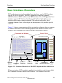
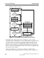
User Interface Overview..................................................................................... 1-9
Command Line Window ................................................................................ 1-10
Control Panel Window................................................................................... 1-14
Getting Help ................................................................................................... 1-15
Running Batch Mode Using Dofiles .............................................................. 1-18
Generating a Log File..................................................................................... 1-19
Running UNIX Commands............................................................................ 1-20
Interrupting the Session.................................................................................. 1-20
Exiting the Session......................................................................................... 1-20
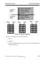
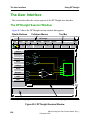
BIST Unified User Interface............................................................................. 1-21
MBISTArchitect User Interface ....................................................................... 1-23
LBIST User Interface ....................................................................................... 1-25
BSDArchitect User Interface ............................................................................ 1-27
DFTAdvisor User Interface .............................................................................. 1-29
FastScan User Interface .................................................................................... 1-31
FlexTest User Interface..................................................................................... 1-33
ASIC/IC Design-for-Test Process Guide, V8.6_1
December 1997
iii
Table of Contents
TABLE OF CONTENTS [continued]
Chapter 2
Understanding DFT Basics................................................................................. 2-1
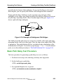
Understanding BIST ........................................................................................... 2-2
Benefits of Memory BIST................................................................................ 2-2
BIST Overview ................................................................................................ 2-3
Memory BIST Overview.................................................................................. 2-3
Simple Memory BIST Architecture ................................................................. 2-4
Memory BIST Insertion with MBISTArchitect............................................... 2-5
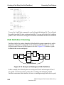
Understanding Boundary Scan ........................................................................... 2-7
Benefits of Boundary Scan............................................................................... 2-7
Boundary Scan Overview ................................................................................ 2-7
Boundary Scan Insertion with BSDArchitect ................................................ 2-13
Understanding Scan Design.............................................................................. 2-14
Internal Scan Circuitry ................................................................................... 2-14
Scan Design Overview ................................................................................... 2-15
Understanding Full Scan ................................................................................ 2-17
Understanding Partial Scan ............................................................................ 2-18
Choosing Between Full or Partial Scan ......................................................... 2-20
Understanding Partition Scan......................................................................... 2-21
Understanding Test Points ............................................................................. 2-23
Test Structure Insertion with DFTAdvisor .................................................... 2-25
Understanding ATPG ....................................................................................... 2-27
The ATPG Process ......................................................................................... 2-27
Mentor Graphics ATPG Applications............................................................ 2-29
Full-Scan and Scan Sequential ATPG with FastScan.................................... 2-29
Non- to Full-Scan ATPG with FlexTest ........................................................ 2-30
Understanding Test Types and Fault Models ................................................... 2-31
Test Types ...................................................................................................... 2-32
Fault Modeling ............................................................................................... 2-35
Fault Detection ............................................................................................... 2-43
Fault Classes................................................................................................... 2-44
Testability Calculations.................................................................................. 2-52
iv
ASIC/IC Design-for-Test Process Guide, V8.6_1
December 1997
Table of Contents
TABLE OF CONTENTS [continued]
Chapter 3
Understanding Common Tool Terminology and Concepts ............................. 3-1
Scan Terminology............................................................................................... 3-2
Scan Cells......................................................................................................... 3-2
Scan Chains...................................................................................................... 3-7
Scan Groups ..................................................................................................... 3-7
Scan Clocks...................................................................................................... 3-7
Scan Architectures .............................................................................................. 3-8
Mux-DFF.......................................................................................................... 3-9
Clocked-Scan ................................................................................................... 3-9
LSSD .............................................................................................................. 3-10
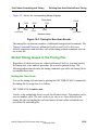
Test Procedure Files ......................................................................................... 3-11
Test Procedure File Rules .............................................................................. 3-11
Test Procedure Statements ............................................................................. 3-12
The Procedures............................................................................................... 3-15
Model Flattening............................................................................................... 3-28
The Flattening Process ................................................................................... 3-29
Simulation Primitives of the Flattened Model ............................................... 3-31
Learning Analysis ............................................................................................. 3-35
Equivalence Relationships ............................................................................. 3-35
Logic Behavior............................................................................................... 3-36
Implied Relationships..................................................................................... 3-36
Forbidden Relationships................................................................................. 3-37
Dominance Relationships............................................................................... 3-38
ATPG Design Rules Checking ......................................................................... 3-38
General Rules Checking................................................................................. 3-39
Procedure Rules Checking ............................................................................. 3-39
Bus Mutual Exclusivity Analysis................................................................... 3-39
Scan Chain Tracing ........................................................................................ 3-40
Shadow Latch Identification .......................................................................... 3-41
Data Rules Checking...................................................................................... 3-41
Transparent Latch Identification .................................................................... 3-41
Clock Rules Checking.................................................................................... 3-42
RAM Rules Checking .................................................................................... 3-42
ASIC/IC Design-for-Test Process Guide, V8.6_1
December 1997
v
Table of Contents
TABLE OF CONTENTS [continued]
Bus Keeper Analysis ...................................................................................... 3-42
Extra Rules Checking..................................................................................... 3-43
Scannability Rules Checking ......................................................................... 3-43
BIST Rules Checking..................................................................................... 3-43
Constrained/Forbidden/Block Value Calculations......................................... 3-44
Chapter 4
Understanding Testability Issues ....................................................................... 4-1
Synchronous Circuitry ........................................................................................ 4-2
Synchronous Design Techniques ..................................................................... 4-2
Asynchronous Circuitry...................................................................................... 4-3
Scannability Checking ........................................................................................ 4-3
Scannability Checking of Latches.................................................................... 4-4
Support for Special Testability Cases................................................................. 4-4
Feedback Loops ............................................................................................... 4-5
Structural Combinational Loops and Loop-Cutting Methods.......................... 4-5
Structural Sequential Loops and Handling .................................................... 4-14
Redundant Logic ............................................................................................ 4-16
Asynchronous Sets and Resets....................................................................... 4-16
Gated Clocks .................................................................................................. 4-17
Tri-State Devices............................................................................................ 4-18
Non-Scan Cell Handling ................................................................................ 4-19
Clock Dividers ............................................................................................... 4-26
Pulse Generators............................................................................................. 4-27
JTAG-Based Circuits ..................................................................................... 4-28
Built-In Self-Test (FastScan Only) ................................................................ 4-28
Testing with RAM and ROM......................................................................... 4-34
Chapter 5
Memory BIST Synthesis ..................................................................................... 5-1
MBISTArchitect Overview ................................................................................ 5-2
Features ............................................................................................................ 5-2
Memory Test Problems .................................................................................... 5-3
MBISTArchitect Solutions............................................................................... 5-3
vi
ASIC/IC Design-for-Test Process Guide, V8.6_1
December 1997
Table of Contents
TABLE OF CONTENTS [continued]
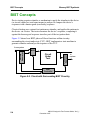
BIST Concepts.................................................................................................... 5-4
BIST Memory Model....................................................................................... 5-5
Memory Testing and Fault Types....................................................................... 5-7
Stuck-at Faults.................................................................................................. 5-7
Transition Faults............................................................................................... 5-8
Coupling Faults ................................................................................................ 5-8
Neighborhood Pattern Sensitive Faults.......................................................... 5-10
Memory BIST Algorithms................................................................................ 5-11
March C.......................................................................................................... 5-12
March C-/March1........................................................................................... 5-14
March C+/March2.......................................................................................... 5-14
March3 ........................................................................................................... 5-17
Col_March1.................................................................................................... 5-17
Unique Address .............................................................................................. 5-18
Checkerboard ................................................................................................. 5-21
Topchecker Algorithm ................................................................................... 5-22
Diagonal ......................................................................................................... 5-23
ROM Test Algorithm ..................................................................................... 5-24
Port Interaction Test Algorithm ..................................................................... 5-24
MBISTArchitect Structures .............................................................................. 5-27
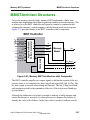
BIST Controller Inputs................................................................................... 5-28
BIST Controller Outputs ................................................................................ 5-29
Compressor Inputs ......................................................................................... 5-31
Compressor Outputs....................................................................................... 5-32
MBISTArchitect Input and Output ................................................................... 5-32
MBISTArchitect Inputs.................................................................................. 5-33
MBISTArchitect outputs................................................................................ 5-35
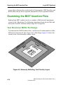
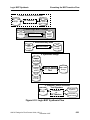
Examining the MBISTArchitect Flow.............................................................. 5-39
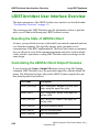
MBISTArchitect User Interface Overview....................................................... 5-42
Resetting the State of MBISTArchitect ......................................................... 5-42
Customizing the MBISTArchitect Output Filenames.................................... 5-42
Inserting Memory BIST Logic ......................................................................... 5-45
A Basic MBISTArchitect Session Using Defaults......................................... 5-46
BIST Circuitry Variations................................................................................. 5-48
Defining Algorithms ...................................................................................... 5-49
ASIC/IC Design-for-Test Process Guide, V8.6_1
December 1997
vii
Table of Contents
TABLE OF CONTENTS [continued]
Generating BIST Structures Using Comparators ........................................... 5-49
Generating BIST Structures using Compressors............................................ 5-54
Adding Pipeline Registers.............................................................................. 5-56
Generating the Comparator Functional Test .................................................. 5-58
Performing Sequential Memory Tests ........................................................... 5-59
Address and Data Scrambling Support .......................................................... 5-60
Verifying Memory BIST Logic ........................................................................ 5-61
Synthesizing Your Design ................................................................................ 5-67
Verifying the Gate-Level Design...................................................................... 5-69
Chapter 6
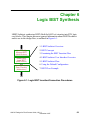
Logic BIST Synthesis .......................................................................................... 6-1
LBISTArchitect Overview.................................................................................. 6-2
Features ............................................................................................................ 6-2
LBISTArchitect Solutions to the Test Challenge............................................. 6-3
LBISTArchitect Input and Output ................................................................... 6-4
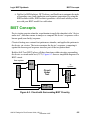
BIST Concepts.................................................................................................... 6-5
Scan-based BIST Configuration ...................................................................... 6-6
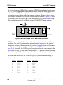
Pattern Generation with LFSRs ....................................................................... 6-7
Test Signature Compression ............................................................................ 6-9
Common LFSR Considerations ..................................................................... 6-10
Issues with Pseudorandom Testing ................................................................ 6-11
Multiphase Test Point Insertion Analysis ...................................................... 6-12
Other Controls................................................................................................ 6-13
Design Considerations for BIST....................................................................... 6-15
X generation and propagation ........................................................................ 6-15
Logic BIST RAM Support ............................................................................. 6-17
How Logic BIST Handles Non-scan Elements.............................................. 6-17
Examining the BIST Insertion Flow................................................................. 6-18
Test Structures Within the Design ................................................................. 6-18
DFT Tool Support for BIST........................................................................... 6-19
BIST Insertion Flows ..................................................................................... 6-20
LBISTArchitect User Interface Overview........................................................ 6-22
Resetting the State of LBISTArchitect .......................................................... 6-22
Customizing the LBISTArchitect Output Filenames..................................... 6-22
viii
ASIC/IC Design-for-Test Process Guide, V8.6_1
December 1997
Table of Contents
TABLE OF CONTENTS [continued]
LBISTArchitect Flow ....................................................................................... 6-24
Using the Default Configuration ...................................................................... 6-25
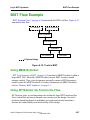
BIST Flow Example ......................................................................................... 6-27
Using MBISTArchitect .................................................................................. 6-27
Using DFTAdvisor Up Front in the Flow ...................................................... 6-27
Using LBISTArchitect ................................................................................... 6-33
Using BSDArchitect....................................................................................... 6-38
Synthesizing the Design................................................................................. 6-40
Using FastScan at the End of the Flow .......................................................... 6-42
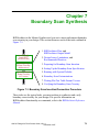
Chapter 7
Boundary Scan Synthesis.................................................................................... 7-1
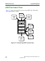
BSDArchitect Flow ............................................................................................ 7-2
BSDArchitect Output Model .............................................................................. 7-4
Design Issues ...................................................................................................... 7-4
Logic Type of Entity Ports............................................................................... 7-5
Handling Tri-state and Bidirectional Ports ...................................................... 7-5
Escaped Identifiers for Verilog ...................................................................... 7-13
Limitations ........................................................................................................ 7-14
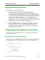
Recommended Practices ................................................................................... 7-17
Preparing for Boundary Scan Insertion ............................................................ 7-17
Boundary Scan Example Design.................................................................... 7-17
Creating the HDL Description ....................................................................... 7-18
Creating the Package Mapping File ............................................................... 7-18
Invoking BSDArchitect.................................................................................. 7-19
Getting Help on BSDArchitect ...................................................................... 7-19
Resetting the State of BSDArchitect.............................................................. 7-20
Exiting the Tool.............................................................................................. 7-20
Setting Up the Boundary Scan Specification.................................................... 7-20
Running with System Defaults ......................................................................... 7-21
Boundary Scan Customizations ........................................................................ 7-23
Creating Customizations ................................................................................ 7-23
Using a Pin Mapping File .............................................................................. 7-26
Technology-Specific Cell Mapping ............................................................... 7-29
Using User-defined Instructions .................................................................... 7-33
ASIC/IC Design-for-Test Process Guide, V8.6_1
December 1997
ix
Table of Contents
TABLE OF CONTENTS [continued]
Connecting Internal Scan Circuitry................................................................ 7-35
Using Memory BIST with Boundary Scan: ................................................... 7-46
Writing FlexTest Table Format Vectors........................................................... 7-49
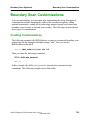
Verifying the Boundary Scan Circuitry ............................................................ 7-50
Test Driver Overview..................................................................................... 7-50
Compiling the HDL Source ........................................................................... 7-51
Running the Verification................................................................................ 7-52
Synthesizing the Boundary Scan.................................................................... 7-55
Verifying the Gate-Level Boundary Scan Logic ........................................... 7-58
Chapter 8
Inserting Internal Scan
and Test Circuitry................................................................................................ 8-1
Understanding DFTAdvisor ............................................................................... 8-2
The DFTAdvisor Process Flow........................................................................ 8-3
DFTAdvisor Inputs and Outputs...................................................................... 8-5
Test Structures Supported by DFTAdvisor...................................................... 8-7
Invoking DFTAdvisor.................................................................................... 8-10
Preparing for Test Structure Insertion .............................................................. 8-11
Selecting the Scan Methodology.................................................................... 8-11
Enabling Test Logic Insertion........................................................................ 8-11
Specifying Clock Signals ............................................................................... 8-14
Specifying Existing Scan Information ........................................................... 8-15
Deleting Existing Scan Circuitry ................................................................... 8-16
Handling Existing Boundary Scan Circuitry.................................................. 8-17
Changing the System Mode (Running Rules Checking) ............................... 8-17
Identifying Test Structures ............................................................................... 8-18
Selecting the Type of Test Structure .............................................................. 8-18
Setting Up for Full Scan Identification .......................................................... 8-19
Setting Up for Clocked Sequential Identification .......................................... 8-19
Setting Up for Sequential Transparent Identification .................................... 8-20
Setting Up for Partition Scan Identification................................................... 8-20
Setting Up for Sequential (ATPG, SCOAP, and Structure) Identification .... 8-23
Setting Up for Test Point Identification ......................................................... 8-24
Manually Including and Excluding Cells for Scan ........................................ 8-28
x
ASIC/IC Design-for-Test Process Guide, V8.6_1
December 1997
Table of Contents
TABLE OF CONTENTS [continued]
Reporting Scannability Information............................................................... 8-30
Running the Identification Process ................................................................ 8-31
Reporting Identification Information ............................................................. 8-31
Inserting Test Structures ................................................................................... 8-32
Setting Up for Internal Scan Insertion ........................................................... 8-32
Setting Up for Test Point Insertion ................................................................ 8-34
Buffering Test Pins ........................................................................................ 8-35
Running the Insertion Process........................................................................ 8-35
Saving the New Design and ATPG Setup ........................................................ 8-39
Writing the Netlist.......................................................................................... 8-39
Writing the Test Procedure File and Dofile for ATPG .................................. 8-40
Running Rules Checking on the New Design................................................ 8-40
Exiting DFTAdvisor....................................................................................... 8-41
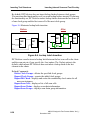
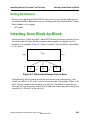
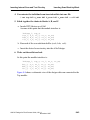
Inserting Scan Block-by-Block......................................................................... 8-41
Verilog and EDIF Flow Example .................................................................. 8-42
Genie Flow Considerations ............................................................................ 8-44
Chapter 9
Generating Test Patterns .................................................................................... 9-1
Understanding FastScan and FlexTest................................................................ 9-2
FastScan and FlexTest Basic Tool Flow.......................................................... 9-3
FastScan and FlexTest Inputs and Outputs ...................................................... 9-6
Understanding FastScan’s ATPG Method ....................................................... 9-8
Understanding FlexTest’s ATPG Method ..................................................... 9-14
Performing Basic Operations............................................................................ 9-19
Invoking the Applications .............................................................................. 9-20
Issuing an Operating System Command ........................................................ 9-23
Setting the System Mode ............................................................................... 9-23
Setting Up Design and Tool Behavior.............................................................. 9-24
Setting Up the Circuit Behavior..................................................................... 9-24
Setting Up Tool Behavior .............................................................................. 9-27
Setting the Circuit Timing (FlexTest Only) ................................................... 9-33
Defining the Scan Data .................................................................................. 9-37
Setting Up for BIST (FastScan Only) ............................................................ 9-40
Checking Rules and Debugging Rules Violations............................................ 9-44
ASIC/IC Design-for-Test Process Guide, V8.6_1
December 1997
xi
Table of Contents
TABLE OF CONTENTS [continued]
Running Good/Fault Simulation on Existing Patterns...................................... 9-45
Fault Simulation ............................................................................................. 9-45
Good Machine Simulation ............................................................................. 9-50
Running Random/BIST Pattern Simulation (FastScan) ................................... 9-52
Random Pattern Simulation ........................................................................... 9-52
BIST Pattern Simulation ................................................................................ 9-53
Obtaining Optimum BIST Coverage ............................................................. 9-55
Example ATPG Run on a BIST Circuit......................................................... 9-58
Setting Up the Fault Information for ATPG..................................................... 9-61
Changing to the ATPG System Mode............................................................ 9-61
Setting the Fault Type .................................................................................... 9-62
Creating the Faults List .................................................................................. 9-62
Adding Faults to an Existing List................................................................... 9-63
Loading Faults from an External List ............................................................ 9-63
Writing Faults to an External File.................................................................. 9-64
Setting the Fault Sampling Percentage (FlexTest Only)................................ 9-64
Setting the Fault Mode ................................................................................... 9-64
Setting the Hypertrophic Limit (FlexTest Only)............................................ 9-65
Setting the Possible-Detect Credit ................................................................. 9-65
Running ATPG ................................................................................................. 9-66
Setting Up for ATPG ..................................................................................... 9-67
Performing a Default ATPG Run................................................................... 9-71
Compressing Patterns..................................................................................... 9-71
Approaches for Improving ATPG Efficiency ................................................ 9-73
Saving the Test Patterns ................................................................................. 9-78
Creating an IDDQ Test Set............................................................................... 9-79
Creating a Selective IDDQ Test Set............................................................... 9-79
Generating a Supplemental IDDQ Test Set ................................................... 9-82
Specifying IDDQ Checks and Constraints..................................................... 9-84
Creating a Path Delay Test Set (FastScan) ....................................................... 9-85
Path Delay Fault Detection ............................................................................ 9-85
The Path Definition File................................................................................. 9-90
Path Definition Checking............................................................................... 9-92
Basic Path Delay Test Procedure ................................................................... 9-93
Path Delay Testing Limitations...................................................................... 9-94
xii
ASIC/IC Design-for-Test Process Guide, V8.6_1
December 1997
Table of Contents
TABLE OF CONTENTS [continued]
Generating Patterns for a Boundary Scan Circuit............................................. 9-94
Dofile and Explanation .................................................................................. 9-95
TAP Controller State Machine....................................................................... 9-96
Test Procedure File and Explanation ............................................................. 9-97
Creating Instruction-Based Test Sets (FlexTest) ............................................ 9-102
Instruction-Based Fault Detection................................................................ 9-102
Instruction File Format................................................................................. 9-104
Verifying Design and Test Pattern Timing..................................................... 9-106
Simulating the Design with Timing ............................................................. 9-106
Checking for Clock-Skew Problems with Mux-DFF Designs..................... 9-110
Chapter 10
Test Pattern Formatting and Timing ............................................................... 10-1
Test Pattern Timing Overview.......................................................................... 10-2
Timing Terminology......................................................................................... 10-2
Defining Scan-Related Event Timing............................................................... 10-3
Converting Test Procedures to Test Cycles ................................................... 10-4
Test Procedure Timing Examples .................................................................. 10-5
Test Procedure Timing Issues ...................................................................... 10-11
Defining Non-Scan Related Event Timing..................................................... 10-13
FastScan Non-Scan Event Timing ............................................................... 10-13
FlexTest Non-Scan Event Timing................................................................ 10-17
Global Timing Issues in the Timing File ..................................................... 10-19
Performing Timing Checks for Tester Formats.............................................. 10-20
Tester Format Restrictions for FastScan ...................................................... 10-21
Tester Format Restrictions for FlexTest ...................................................... 10-23
Saving the Patterns ......................................................................................... 10-23
Features of the Formatter ............................................................................. 10-24
Pattern Formatting Issues............................................................................ 10-25
Saving Patterns in Basic Test Data Formats ................................................ 10-27
Saving in ASIC Vendor Data Formats......................................................... 10-40
ASIC/IC Design-for-Test Process Guide, V8.6_1
December 1997
xiii
Table of Contents
TABLE OF CONTENTS [continued]
Chapter 11
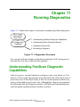
Running Diagnostics ......................................................................................... 11-1
Understanding FastScan Diagnostic Capabilities ............................................. 11-1
Understanding Stuck Faults and Defects .......................................................... 11-3
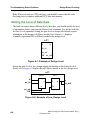
Creating the Failure File ................................................................................... 11-4
Failure File Format......................................................................................... 11-5
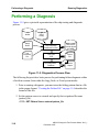
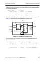
Performing a Diagnosis .................................................................................... 11-6
Appendix A
Design Rules Checking........................................................................................A-1
FastScan Rules Checking ...................................................................................A-1
DFTAdvisor Rules Checking .............................................................................A-1
FlexTest Rules Checking ....................................................................................A-2
Troubleshooting Rules Violations ......................................................................A-2
Setting the Handling of Rules ..........................................................................A-2
Turning on ATPG Analysis .............................................................................A-3
Setting the Level of Gate Data .........................................................................A-4
Setting the Gate Information Type...................................................................A-6
Reporting Gate Data.........................................................................................A-7
The Design Rules..............................................................................................A-11
General Rules .................................................................................................A-11
Procedure Rules .............................................................................................A-14
Scan Chain Trace Rules .................................................................................A-28
Scan Cell Data Rules......................................................................................A-35
Clock Rules ....................................................................................................A-46
RAM Rules.....................................................................................................A-72
BIST Rules .....................................................................................................A-78
Extra Rules .....................................................................................................A-82
Scannability Rules..........................................................................................A-93
Appendix B
Using DFTInsight ................................................................................................B-1
Overview of DFTInsight.....................................................................................B-1
xiv
ASIC/IC Design-for-Test Process Guide, V8.6_1
December 1997
Table of Contents
TABLE OF CONTENTS [continued]
Inputs and Outputs ..........................................................................................B-3
DFTInsight Features.........................................................................................B-4
The User Interface ..............................................................................................B-6
The DFTInsight Session Window....................................................................B-6
Areas of the Session Window ..........................................................................B-7
Schematic Display Actions ..............................................................................B-7
Pulldown Menu Selections...............................................................................B-8
Tool Bar Selections ........................................................................................B-10
Palette Buttons ...............................................................................................B-11
Accessing Tool Functionality ...........................................................................B-12
Performing Basic Tasks ....................................................................................B-14
Invoking DFTInsight......................................................................................B-15
Interrupting Operations ..................................................................................B-15
Selecting the Design Level.............................................................................B-15
Selecting the Gate Data ..................................................................................B-17
Controlling the Displayed Information ..........................................................B-17
Reverting to a Previous Schematic View.......................................................B-19
Displaying Specific Instances ........................................................................B-19
Displaying Instances in a Path .......................................................................B-23
Troubleshooting DRC Violations ..................................................................B-26
Saving and Recalling a Schematic .................................................................B-28
Saving and Replaying the Session Transcript................................................B-28
Printing the Displayed Schematic ..................................................................B-29
Closing the DFTInsight Session.....................................................................B-29
Appendix C
Design Library.....................................................................................................C-1
Defining Scan Information .................................................................................C-1
Defining a Scan Cell Model .............................................................................C-2
Example Scan Definitions................................................................................C-6
Defining a Model ..............................................................................................C-10
Model_name...................................................................................................C-10
List_of_pins....................................................................................................C-11
Interface Pins and Internal Nodes ..................................................................C-11
Cell Type........................................................................................................C-14
ASIC/IC Design-for-Test Process Guide, V8.6_1
December 1997
xv
Table of Contents
TABLE OF CONTENTS [continued]
Attributes........................................................................................................C-14
Internal Faults.................................................................................................C-31
Support of Arrays Within Library Models.....................................................C-36
Defining Macros ...............................................................................................C-37
Using Model Aliases.........................................................................................C-37
Reading Multiple Libraries...............................................................................C-38
Supported Primitives ........................................................................................C-39
AND Gate.......................................................................................................C-39
NAND Gate....................................................................................................C-40
OR Gate..........................................................................................................C-41
NOR Gate.......................................................................................................C-42
Inverter ...........................................................................................................C-43
Buffer .............................................................................................................C-44
Buffer With High Impedance Output.............................................................C-44
XOR Gate.......................................................................................................C-46
XNOR Gate ....................................................................................................C-47
Tri-State Buffer with Active Low Control.....................................................C-48
Inverted Tri-State Buffer with Active Low Control ......................................C-49
Tri-State Buffer with Active High Control ....................................................C-50
Inverted Tri-State Buffer with Active High Control......................................C-51
Multiplexer.....................................................................................................C-52
D Flip-Flop.....................................................................................................C-53
D Latch...........................................................................................................C-55
One Time Unit Delay Element.......................................................................C-57
Feedback Inverter...........................................................................................C-58
Wire Element .................................................................................................C-59
Pull-Up or Pull-Down Device........................................................................C-60
Power Signal ..................................................................................................C-61
Ground Signal ................................................................................................C-61
Unknown Signal.............................................................................................C-62
High Impedance Signal ..................................................................................C-62
Undefined .......................................................................................................C-63
Unidirectional NMOS Transistor...................................................................C-64
Unidirectional PMOS Transistor....................................................................C-65
Unidirectional Resistive NMOS Transistor ...................................................C-66
xvi
ASIC/IC Design-for-Test Process Guide, V8.6_1
December 1997
Table of Contents
TABLE OF CONTENTS [continued]
Unidirectional Resistive PMOS Transistor....................................................C-67
Unidirectional Feedback NMOS Transistor...................................................C-67
Unidirectional Feedback PMOS Transistor ...................................................C-68
Unidirectional CMOS1 Transistor .................................................................C-70
Unidirectional CMOS2 Transistor .................................................................C-71
Unidirectional Resistive CMOS1 Transistor .................................................C-72
Unidirectional Resistive CMOS2 Transistor .................................................C-73
Unidirectional Feedback CMOS1 Transistor.................................................C-74
Unidirectional Feedback CMOS2 Transistor.................................................C-75
Pulse Generators with User Defined Timing .................................................C-76
RAM and ROM..............................................................................................C-78
Appendix D
Using VHDL.........................................................................................................D-1
Overview of VHDL Support ..............................................................................D-1
Reading VHDL ...................................................................................................D-2
Writing VHDL....................................................................................................D-4
Appendix E
Spice Netlist Support........................................................................................... E-1
Spice Overview................................................................................................... E-1
Spice Netlist Reader ........................................................................................... E-1
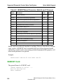
Supported Elements & Control Spice Card Syntax ............................................ E-3
Title/END card ................................................................................................. E-3
Resistor Card.................................................................................................... E-3
Capacitor Card ................................................................................................. E-4
MOSFET Card ................................................................................................. E-5
MODEL Card................................................................................................... E-6
SUBCKT Card ................................................................................................. E-8
SUBCKT Call Card........................................................................................ E-10
OPTIONS Card .............................................................................................. E-10
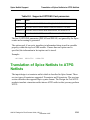
Translation of Spice Netlists to ATPG Netlists ................................................ E-11
Procedures and Requirements ........................................................................ E-12
Matching Algorithm....................................................................................... E-13
ASIC/IC Design-for-Test Process Guide, V8.6_1
December 1997
xvii
Table of Contents
TABLE OF CONTENTS [continued]
Direction Assignment..................................................................................... E-13
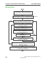
Process Flow .................................................................................................. E-14
Spice Commands .............................................................................................. E-15
Index
xviii
ASIC/IC Design-for-Test Process Guide, V8.6_1
December 1997
Table of Contents
LIST OF FIGURES
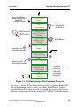
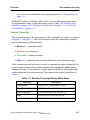
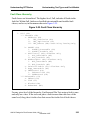
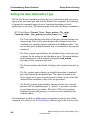
Figure 1. DFT Documentation Roadmap .......................................................xxxiv
Figure 1-1. Top-Down Design Flow Tasks and Products ................................. 1-3
Figure 1-2. ASIC/IC Design-for-Test Tasks ..................................................... 1-6
Figure 1-3. Common Elements of the DFT Graphical User Interfaces ............. 1-9
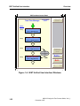
Figure 1-4. BIST Unified User Interface Windows........................................ 1-22
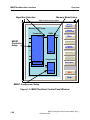
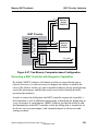
Figure 1-5. MBISTArchitect Control Panel Window...................................... 1-24
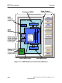
Figure 1-6. LBISTArchitect Control Panel Window....................................... 1-26
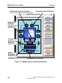
Figure 1-7. BSDArchitect Control Panel Window .......................................... 1-28
Figure 1-8. DFTAdvisor Control Panel Window ............................................ 1-30
Figure 1-9. FastScan Control Panel Window .................................................. 1-32
Figure 1-10. FlexTest Control Panel Window................................................. 1-34
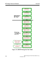
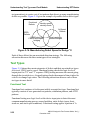
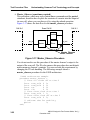
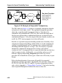
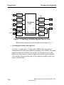
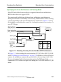
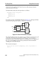
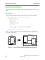
Figure 2-1. DFT Concepts ................................................................................. 2-1
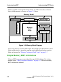
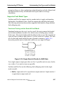
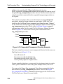
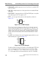
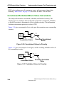
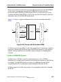
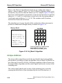
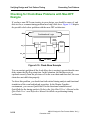
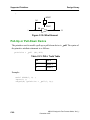
Figure 2-2. Memory Block Diagram ................................................................. 2-4
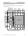
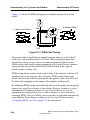
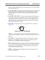
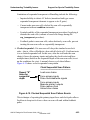
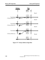
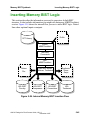
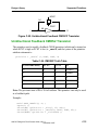
Figure 2-3. Basic Memory BIST Block Diagram.............................................. 2-5
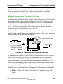
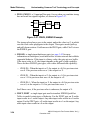
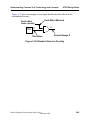
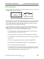
Figure 2-4. Boundary Scan Chips on Board ...................................................... 2-8
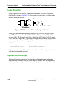
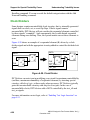
Figure 2-5. Boundary Scan Architecture ........................................................... 2-9
Figure 2-6. Design Before and After Adding Scan ......................................... 2-16
Figure 2-7. Full Scan Representation .............................................................. 2-17
Figure 2-8. Partial Scan Representation .......................................................... 2-19
Figure 2-9. Full, Partial, and Non-Scan Trade-offs ......................................... 2-20
Figure 2-10. Example of Partitioned Design ................................................... 2-22
Figure 2-11. Partition Scan Circuitry Added to Partition A ............................ 2-23
Figure 2-12. Uncontrollable and Unobservable Circuitry ............................... 2-24
Figure 2-13. Testability Benefits from Test Point Circuitry............................ 2-24
Figure 2-14. Manufacturing Defect Space for Design "X ............................... 2-32
Figure 2-15. Internal Faulting Example........................................................... 2-36
Figure 2-16. Single Stuck-At Faults for AND Gate ........................................ 2-37
Figure 2-17. IDDQ Fault Testing .................................................................... 2-40
Figure 2-18. Transition Fault Detection Process ............................................. 2-41
Figure 2-19. Fault Detection Process............................................................... 2-43
Figure 2-20. Path Sensitization Example......................................................... 2-44
Figure 2-21. Example of "Unused" Fault in Circuitry..................................... 2-45
Figure 2-22. Example of “Tied” Fault in Circuitry ......................................... 2-46
Figure 2-23. Example of “Blocked” Fault in Circuitry ................................... 2-46
Figure 2-24. Example of "Redundant" Fault in Circuitry................................ 2-47
xix
ASIC/IC Design-for-Test Process Guide, V8.6_1
December 1997
Table of Contents
LIST OF FIGURES [continued]
Figure 2-25. Fault Class Hierarchy.................................................................. 2-51
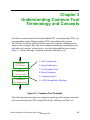
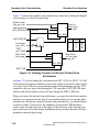
Figure 3-1. Common Tool Concepts ................................................................. 3-1
Figure 3-2. Generic Scan Cell ........................................................................... 3-2
Figure 3-3. Generic Mux-DFF Scan Cell Implementation ................................ 3-3
Figure 3-4. LSSD Master/Slave Element Example ........................................... 3-4
Figure 3-5. Mux-DFF/Shadow Element Example............................................. 3-5
Figure 3-6. Mux-DFF/Copy Element Example ................................................. 3-6
Figure 3-7. Generic Scan Chain......................................................................... 3-7
Figure 3-8. Scan Clocks Example ..................................................................... 3-8
Figure 3-9. Mux-DFF Replacement .................................................................. 3-9
Figure 3-10. Clocked-Scan Replacement ........................................................ 3-10
Figure 3-11. LSSD Replacement ..................................................................... 3-10
Figure 3-12. Shift Procedure............................................................................ 3-15
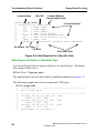
Figure 3-13. Timing Diagram for Shift Procedure .......................................... 3-17
Figure 3-14. Load_Unload Procedure ............................................................. 3-18
Figure 3-15. Timing Diagram for Load_Unload Procedure ............................ 3-20
Figure 3-16. Shadow_Control Procedure ........................................................ 3-21
Figure 3-17. Master_Observe Procedure ......................................................... 3-22
Figure 3-18. Shadow_Observe Procedure ....................................................... 3-23
Figure 3-19. Sequential Transparent Circuitry Example ................................. 3-24
Figure 3-20. Skew_Load Procedure ................................................................ 3-26
Figure 3-21. Skew_load applied within Pattern .............................................. 3-27
Figure 3-22. Design Before Flattening ............................................................ 3-30
Figure 3-23. Design After Flattening............................................................... 3-30
Figure 3-24. 2x1 MUX Example ..................................................................... 3-32
Figure 3-25. LA, DFF Example....................................................................... 3-32
Figure 3-26. TSD, TSH Example .................................................................... 3-33
Figure 3-27. PBUS, SWBUS Example............................................................ 3-34
Figure 3-28. Equivalence Relationship Example ............................................ 3-35
Figure 3-29. Example of Learned Logic Behavior .......................................... 3-36
Figure 3-30. Example of Implied Relationship Learning ................................ 3-37
Figure 3-31. Forbidden Relationship Example................................................ 3-37
Figure 3-32. Dominance Relationship Example.............................................. 3-38
Figure 3-33. Bus Contention Example ............................................................ 3-39
Figure 3-34. Bus Contention Analysis............................................................. 3-40
xx
ASIC/IC Design-for-Test Process Guide, V8.6_1
December 1997
Table of Contents
LIST OF FIGURES [continued]
Figure 3-35. Simulation Model with Bus Keeper............................................ 3-42
Figure 3-36. Constrained Values in Circuitry.................................................. 3-44
Figure 3-37. Forbidden Values in Circuitry .................................................... 3-44
Figure 3-38. Blocked Values in Circuitry........................................................ 3-45
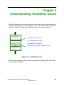
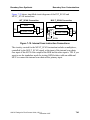
Figure 4-1. Testability Issues............................................................................. 4-1
Figure 4-2. Structural Combinational Loop Example ....................................... 4-5
Figure 4-3. Loop Naturally-Blocked by Constant Value................................... 4-6
Figure 4-4. Cutting Constant Value Loops........................................................ 4-6
Figure 4-5. Cutting Single Multiple-Fanout Loops ........................................... 4-7
Figure 4-6. Loop Candidate for Duplication ..................................................... 4-8
Figure 4-7. TIE-X Insertion Simulation Pessimism .......................................... 4-8
Figure 4-8. Cutting Loops by Gate Duplication ................................................ 4-9
Figure 4-9. Cutting Coupling Loops................................................................ 4-10
Figure 4-10. Delay Element Added to Feedback Loop ................................... 4-11
Figure 4-11. "Fake" Feedback Loop................................................................ 4-12
Figure 4-12. Sequential Feedback Loop .......................................................... 4-14
Figure 4-13. Fake Sequential Loop ................................................................. 4-15
Figure 4-14. Test Logic Added to Control Asynchronous Reset .................... 4-17
Figure 4-15. Test Logic Added to Control Gated Clock ................................. 4-18
Figure 4-16. Tri-state Bus Contention ............................................................. 4-19
Figure 4-17. Requirement for Combinationally Transparent Latches............. 4-20
Figure 4-18. Example of Sequential Transparency ......................................... 4-22
Figure 4-19. Clocked Sequential Scan Pattern Events .................................... 4-23
Figure 4-20. Clock Divider.............................................................................. 4-26
Figure 4-21. Example Pulse Generator Circuitry ............................................ 4-27
Figure 4-22. LFSR Configuration.................................................................... 4-29
Figure 4-23. Simple BIST Configuration ........................................................ 4-30
Figure 4-24. Design with Embedded RAM ..................................................... 4-35
Figure 4-25. RAM Sequential Example .......................................................... 4-38
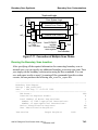
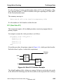
Figure 5-1. Memory BIST Insertion/Connection Procedures............................ 5-1
Figure 5-2. Circuit with Surrounding BIST Circuitry ....................................... 5-4
Figure 5-3. BIST Hierarchy ............................................................................... 5-6
Figure 5-4. Stuck-at Fault State Diagram .......................................................... 5-7
Figure 5-5. Transition Fault ............................................................................... 5-8
Figure 5-6. Transition Fault State Diagram ....................................................... 5-8
ASIC/IC Design-for-Test Process Guide, V8.6_1
December 1997
xxi
Table of Contents
LIST OF FIGURES [continued]
Figure 5-7. Inversion Coupling Fault ................................................................ 5-9
Figure 5-8. Idempotent Coupling Fault ............................................................. 5-9
Figure 5-9. Neighborhood Pattern Sensitive Fault .......................................... 5-10
Figure 5-10. March C Algorithm..................................................................... 5-13
Figure 5-11. March C- (or March1) Algorithm ............................................... 5-14
Figure 5-12. Modified March C Algorithm ..................................................... 5-15
Figure 5-13. March C+ (or March2) Algorithm .............................................. 5-15
Figure 5-14. March2 Algorithm with Varied Background .............................. 5-16
Figure 5-15. March3 Algorithm ...................................................................... 5-17
Figure 5-16. Col_March1 Algorithm............................................................... 5-18
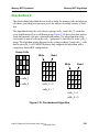
Figure 5-17. Unique Address Algorithm ......................................................... 5-20
Figure 5-18. Checkerboard Algorithm ............................................................ 5-21
Figure 5-19. Diagonal Algorithm .................................................................... 5-23
Figure 5-20. ROM Algorithm.......................................................................... 5-24
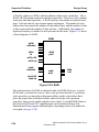
Figure 5-21. Memory BIST Architecture with Comparator ............................ 5-27
Figure 5-22. Memory BIST Architecture with a Compressor ......................... 5-30
Figure 5-23. Compressor Downstream from the Ram..................................... 5-31
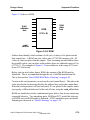
Figure 5-24. MBISTArchitect Inputs and Outputs .......................................... 5-32
Figure 5-25. Memory BIST in a Larger DFT Design Flow ............................ 5-40
Figure 5-26. Internal Memory BIST Insertion Flow ....................................... 5-45
Figure 5-27. Two Memory Comparator-based Configuration ........................ 5-51
Figure 5-28. BIST Architecture Using Diagnostic Functionality.................... 5-52
Figure 5-29. One Compressor for Three Memories ........................................ 5-56
Figure 5-30. Pipeline Registers Example ........................................................ 5-57
Figure 5-31. Simulation Results Partial Waveform......................................... 5-66
Figure 6-1. Logic BIST Insertion/Connection Procedures ................................ 6-1
Figure 6-2. LBISTArchitect Inputs and Outputs ............................................... 6-4
Figure 6-3. Circuit with Surrounding BIST Circuitry ....................................... 6-5
Figure 6-4. Logic BIST Architecture................................................................. 6-7
Figure 6-5. Four-Stage LFSR with One Tap Point............................................ 6-8
Figure 6-6. Eight-Stage MISR Connecting to Two Scan Chains ...................... 6-9
Figure 6-7. Eight-Stage LFSR Configurations ................................................ 6-11
Figure 6-8. RUNBIST Function ...................................................................... 6-14
Figure 6-9. Hierarchy Reflecting Test Circuitry Layers.................................. 6-18
Figure 6-10. Logic BIST Synthesis Flow ........................................................ 6-21
xxii
ASIC/IC Design-for-Test Process Guide, V8.6_1
December 1997
Table of Contents
LIST OF FIGURES [continued]
Figure 6-11. Internal Logic BIST Insertion Flow............................................ 6-24
Figure 6-12. Tools in BIST.............................................................................. 6-27
Figure 6-13. Synthesis in the BIST Flow ........................................................ 6-40
Figure 7-1. Boundary Scan Insertion/Connection Procedure ............................ 7-1
Figure 7-2. BSDArchitect Design Flow ............................................................ 7-2
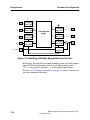
Figure 7-3. Boundary Scan Output Model ........................................................ 7-4
Figure 7-4. Handling of Enable Signals Not Used in Core ............................. 7-10
Figure 7-5. Handling of Enable Signals Used in Core .................................... 7-12
Figure 7-6. Accessing the Enable .................................................................... 7-13
Figure 7-7. Clocking Circuitry Created for Mux-DFF Architecture ............... 7-37
Figure 7-8. Clocking Circuitry Created for Clocked Scan Architecture ......... 7-38
Figure 7-9. Default Architecture for Testing Mode......................................... 7-39
Figure 7-10. Internal Scan Instruction Connections ........................................ 7-41
Figure 7-11. Connection of Multiple Scan Chains .......................................... 7-43
Figure 8-1. Internal Scan Insertion Procedure ................................................... 8-1
Figure 8-2. Basic Scan Insertion Flow with DFTAdvisor ................................. 8-3
Figure 8-3. The Inputs and Outputs of DFTAdvisor ......................................... 8-5
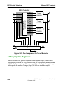
Figure 8-4. DFTAdvisor Supported Test Structures.......................................... 8-7
Figure 8-5. Test Logic Insertion ...................................................................... 8-12
Figure 8-6. Lockup Latch Insertion ................................................................. 8-38
Figure 8-7. Hierarchical Design Prior to Scan................................................. 8-41
Figure 8-8. Final Scan-Inserted Design ........................................................... 8-44
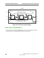
Figure 9-1. Test Generation Procedure.............................................................. 9-1
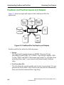
Figure 9-2. Overview of FastScan/FlexTest Usage ........................................... 9-3
Figure 9-3. FastScan/FlexTest Inputs and Outputs............................................ 9-6
Figure 9-4. Clock-PO Circuitry ....................................................................... 9-10
Figure 9-5. Cycle-Based Circuit with Single Phase Clock.............................. 9-15
Figure 9-6. Cycle-Based Circuit with Two Phase Clock................................. 9-16
Figure 9-7. Example Test Cycle ...................................................................... 9-18
Figure 9-8. Data Capture Handling Example .................................................. 9-31
Figure 9-9. Block Diagram of BIST Example Circuit..................................... 9-59
Figure 9-10. Efficient ATPG Flow .................................................................. 9-66
Figure 9-11. Circuitry with Natural “Select” Functionality ............................ 9-69
Figure 9-12. Launch and Capture Events ........................................................ 9-86
Figure 9-13. Robust Detection Example ......................................................... 9-88
ASIC/IC Design-for-Test Process Guide, V8.6_1
December 1997
xxiii
Table of Contents
LIST OF FIGURES [continued]
Figure 9-14. Transition Detection Example .................................................... 9-89
Figure 9-15. Example of Ambiguous Path Definition..................................... 9-92
Figure 9-16. Example of Ambiguous Path Edges ........................................... 9-93
Figure 9-17. State Diagram of TAP Controller Circuitry................................ 9-96
Figure 9-18. Example Instruction File........................................................... 9-105
Figure 9-19. Clock-Skew Example................................................................ 9-110
Figure 10-1. Defining Timing Process Flow ................................................... 10-1
Figure 10-2. Test Cycle Timing for Test_Setup Procedure............................. 10-5
Figure 10-3. Timing for Non-Scan Events .................................................... 10-19
Figure 11-1. Diagnostics Procedure ................................................................ 11-1
Figure 11-2. Diagnostics Process Flow ........................................................... 11-6
Figure A-1. Example of Design Level...............................................................A-4
Figure A-2. Example of Low_Design Level .....................................................A-4
Figure A-3. Example of Primitive Level ...........................................................A-5
Figure A-4. Data Reported for a Specific Gate .................................................A-8
Figure A-5. Rule D10 Violation Example .......................................................A-44
Figure A-6. Rule D11 Violation Example .......................................................A-45
Figure A-7. C1 Rule Example Circuit .............................................................A-50
Figure A-8. C2 Rule Example Circuit .............................................................A-51
Figure A-9. C3 Rule Example Circuit .............................................................A-54
Figure A-10. C4 Rule Example Circuit ...........................................................A-57
Figure A-11. C5 Rule Example Circuit ...........................................................A-59
Figure A-12. C6 Rule Example Circuit ...........................................................A-61
Figure A-13. C7 Rule Example Circuit ...........................................................A-63
Figure A-14. C8 Rule Example Circuit ...........................................................A-65
Figure A-15. C9 Rule Example Circuit ...........................................................A-67
Figure A-16. C10 Rule Example Circuit .........................................................A-68
Figure B-1. DFTInsight Process Within the DFT Tools ...................................B-2
Figure B-2. DFTInsight Inputs and Outputs......................................................B-4
Figure B-3. DFTInsight Session Window .........................................................B-6
Figure B-4. DFTInsight Instance Information.................................................B-16
Figure B-5. DFF Displayed .............................................................................B-22
Figure B-6. Connected Circuitry .....................................................................B-22
Figure B-7. MUX and DFF .............................................................................B-27
Figure C-1. General Scan Definition Replacement Example ............................C-6
xxiv
ASIC/IC Design-for-Test Process Guide, V8.6_1
December 1997
Table of Contents
LIST OF FIGURES [continued]
Figure C-2. Mux-Scan Definition Replacement Example.................................C-7
Figure C-3. Clocked-Scan Definition Replacement Example ...........................C-8
Figure C-4. LSSD Scan Definition Replacement Example...............................C-9
Figure C-5. Bidirectional Buffer......................................................................C-11
Figure C-6. Scan D Flip-Flop ..........................................................................C-11
Figure C-7. Design Example with Bus Keeper ...............................................C-24
Figure C-8. Simulation Model with ZHOLD Bus Keeper ..............................C-24
Figure C-9. Combinational Logic....................................................................C-25
Figure C-10. Creating an Internal Node ..........................................................C-26
Figure C-11. Tri-State Buffer ..........................................................................C-26
Figure C-12. Non-Inverting Buffer..................................................................C-27
Figure C-13. Two-input NAND Gate ..............................................................C-27
Figure C-14. Mux-DFF Scan Cell ...................................................................C-28
Figure C-15. The MUX ...................................................................................C-28
Figure C-16. The DFF .....................................................................................C-29
Figure C-17. Tri-State Gate (_buf primitive) ..................................................C-30
Figure C-18. Tri-State Gate (_bufz primitive).................................................C-30
Figure C-19. Tri-State Gate (_wire primitive).................................................C-31
Figure C-20. Internal Faults.............................................................................C-32
Figure C-21. AND Gate...................................................................................C-40
Figure C-22. NAND Gate................................................................................C-41
Figure C-23. OR Gate......................................................................................C-42
Figure C-24. NOR Gate ...................................................................................C-43
Figure C-25. Inverter .......................................................................................C-43
Figure C-26. Buffer .........................................................................................C-44
Figure C-27. Buffer with High-Impedance Output .........................................C-45
Figure C-28. XOR Gate ...................................................................................C-46
Figure C-29. XNOR Gate ................................................................................C-47
Figure C-30. Tri-State Buffer with Active Low Control .................................C-48
Figure C-31. Inverted Tri-State Buffer with Active Low Control...................C-49
Figure C-32. Tri-State Buffer with Active High Control ................................C-50
Figure C-33. Inverted Tri-State Buffer with Active High Control ..................C-51
Figure C-34. Multiplexer .................................................................................C-53
Figure C-35. D Flip-Flop .................................................................................C-55
Figure C-36. D Latch .......................................................................................C-56
ASIC/IC Design-for-Test Process Guide, V8.6_1
December 1997
xxv
Table of Contents
LIST OF FIGURES [continued]
Figure C-37. One Time Unit Delay Element...................................................C-57
Figure C-38. Feedback Inverter .......................................................................C-58
Figure C-39. Wire Element..............................................................................C-60
Figure C-40. Pull-Up or Pull-Down Device ....................................................C-61
Figure C-41. Undefined Functional Block ......................................................C-64
Figure C-42. Unidirectional NMOS Transistor ...............................................C-65
Figure C-43. Unidirectional PMOS Transistor................................................C-66
Figure C-44. Unidirectional Resistive NMOS Transistor ...............................C-66
Figure C-45. Unidirectional Resistive PMOS Transistor ................................C-67
Figure C-46. Unidirectional Feedback NMOS Transistor...............................C-68
Figure C-47. Unidirectional Feedback PMOS Transistor ...............................C-69
Figure C-48. Unidirectional CMOS1 Transistor .............................................C-70
Figure C-49. Unidirectional CMOS2 Transistor .............................................C-71
Figure C-50. Unidirectional Resistive CMOS1 Transistor..............................C-72
Figure C-51. Unidirectional Resistive CMOS2 Transistor..............................C-73
Figure C-52. Unidirectional Feedback CMOS1F Transistor...........................C-75
Figure C-53. Unidirectional Feedback CMOS2F Transistor...........................C-76
Figure C-54. ROM...........................................................................................C-79
Figure C-55. RAM...........................................................................................C-80
Figure C-56. Flattened RAM Model with oen Set to 0 ...................................C-90
Figure D-1. Example dft.map File .....................................................................D-3
xxvi
ASIC/IC Design-for-Test Process Guide, V8.6_1
December 1997
Table of Contents
LIST OF TABLES
Table 1-1. Session Transcript Popup Menu Items ........................................... 1-11
Table 1-2. Command Transcript Popup Menu Items ...................................... 1-12
Table 2-1. Test Type/Fault Model Relationship .............................................. 2-35
Table 4-1. FastScan BIST Commands ............................................................. 4-32
Table 4-2. FastScan and FlexTest RAM/ROM Commands ............................ 4-41
Table 5-1. Behavior of scan_out and fail_h ports during debug mode ........... 5-53
Table 6-1. Common LFSR Configuration ....................................................... 6-10
Table 8-1. Test Type Interactions ...................................................................... 8-9
Table 9-1. ATPG Constraint Conditions ........................................................ 9-69
Table 9-2. Pin Value Requirements for ADD Instruction ............................. 9-103
Table C-1. AND Truth Table ...........................................................................C-39
Table C-2. NAND Truth Table ........................................................................C-40
Table C-3. OR Truth Table ..............................................................................C-41
Table C-4. NOR Truth Table ...........................................................................C-42
Table C-5. Inverter Truth Table .......................................................................C-43
Table C-6. Buffer Truth Table .........................................................................C-44
Table C-7. BUFZ Truth Table .........................................................................C-45
Table C-8. XOR Truth Table ...........................................................................C-46
Table C-9. XNOR Truth Table ........................................................................C-47
Table C-10. TSL Truth Table ..........................................................................C-48
Table C-11. TSLI Truth Table .........................................................................C-49
Table C-12. TSH Truth Table ..........................................................................C-50
Table C-13. TSHI Truth Table ........................................................................C-51
Table C-14. MUX Truth Table ........................................................................C-52
Table C-15. D Flip-Flop Truth Table for FlexTest ..........................................C-53
Table C-16. D Flip-Flop Truth Table for FastScan .........................................C-54
Table C-17. D Latch Truth Table ....................................................................C-56
Table C-18. DELAY Truth Table ....................................................................C-57
Table C-19. INVF Truth Table ........................................................................C-58
Table C-20. WIRE Truth Table (for two inputs) .............................................C-59
Table C-21. PULL Truth Table .......................................................................C-60
Table C-22. UNDEFINED Truth Table ..........................................................C-63
Table C-23. NMOS Truth Table ......................................................................C-64
Table C-24. PMOS Truth Table ......................................................................C-65
Table C-25. RNMOS Truth Table ...................................................................C-66
xxvii
ASIC/IC Design-for-Test Process Guide, V8.6_1
December 1997
Table of Contents
LIST OF TABLES [continued]
Table C-26. RPMOS Truth Table ....................................................................C-67
Table C-27. NMOSF Truth Table ...................................................................C-68
Table C-28. PMOSF Truth Table ....................................................................C-69
Table C-29. CMOS1 Truth Table ....................................................................C-70
Table C-30. CMOS2 Truth Table ....................................................................C-71
Table C-31. RCMOS1 Truth Table .................................................................C-72
Table C-32. RCMOS2 Truth Table .................................................................C-73
Table C-33. CMOS1F Truth Table ..................................................................C-74
Table C-34. CMOS2F Truth Table ..................................................................C-75
Table E-1. MOSFET Model Parameters (Both N and P Channel) .................... E-6
Table E-2. Supported OPTIONS Card parameters ......................................... E-11
xxviii
ASIC/IC Design-for-Test Process Guide, V8.6_1
December 1997
xxix
ASIC/IC Design-for-Test Process Guide, V8.6_1
December 1997
Table of Contents
LIST OF TABLES [continued]
xxx
ASIC/IC Design-for-Test Process Guide, V8.6_1
December 1997
About This Manual
The ASIC/IC Design-for-Test Process Guide gives an overview of ASIC/IC
Design-for-Test (DFT) strategies and shows the use of Mentor Graphics ASIC/IC
DFT products in the context of typical DFT design process flows. This document
discusses the following Mentor Graphics DFT products: BISTArchitect,
BSDArchitect, DFTAdvisor, FastScan, FlexTest, DFTInsight, and ASIC Vector
Interfaces.
Chapter 1 discusses the basic concepts behind DFT, establishes the framework in
which Mentor Graphic ASIC DFT products are used, and briefly describes each of
these products. Chapter 2 gives conceptual information necessary for determining
what test strategy would work best for you. Chapter 3 provides tool methodology
information, including common terminology and concepts used by the tools.
Chapter 4 outlines characteristics of testable designs and explains how to handle
special design situations that can affect testability. The remaining sections of the
book, sections 5 through 11, discuss the common tasks involved at each step
within a typical process flow using Mentor Graphics DFT tools.
Appendix A lists and explains the design rules that several of the DFT tools check.
Appendix B discusses using the optional schematic viewing tool, DFTInsight, for
debugging rules violations. Appendix C provides DFT library modeling
information. Appendixes D and E provides information on using VHDL and Spice
repectively with Mentor Graphics DFT tools.
This application uses the Adobe Acrobat Reader as its on-line documentation and
help viewer. On-line help requires a Mentor Graphics-supplied software extension
to the Acrobat Reader and also requires setting an environment variable. For more
information, refer to Using Mentor Graphics Documentation with Adobe Acrobat.
ASIC/IC Design-for-Test Process Guide, V8.6_1
December 1997
xxxi
Related Publications
Related Publications
This section gives references to both industry DFT documentation and related
Mentor Graphics product documentation.
General DFT Documentation
The ASIC/IC Design-for-Test Process Guide gives an overview of a variety of
DFT concepts and issues. However, for more detailed information on any of the
topics presented in this document, refer to the following:
• Abramovici, Miron, Melvin A. Breuer, and Arthur D. Friedman. Digital
Systems Testing and Testable Design. New York: Computer Science Press,
1990.
• Huber, John P. and Mark W. Rosneck. Successful ASIC Design the First
Time Through. New York: Van Nostrand Reinhold, 1991.
• McCluskey, Edward J. Logic Design Principles with Emphasis on Testable
Semicustom Circuits. Englewood Cliffs: Prentice-Hall, 1986.
• IEEE Std 1149.1-1990, IEEE Standard Test Access Port and BoundaryScan Architecture. New York: IEEE, 1990.
• Fujiwara, Hideo. Logic Testing and Design for Testability. Cambridge: The
MIT Press, 1985.
• Agarwal, V. D. and S. C. Seth. Test Generation for VLSI Chips. Computer
Society Press, 1988.
Memory BIST Documentation
• van de Goor, A.J. Testing Semiconductor Memories. John Wiley & Sons,
1991.
• Rob Decker, Frans Beenker, (Philips Research Laboratories), “Fault
Modeling and Test Algorithm Development for Static Random Access
Memories”, Proceedings ITC 1988, pp. 343-351.
xxxii
ASIC/IC Design-for-Test Process Guide, V8.6_1
December 1997
Related Publications
IDDQ Documentation
• J. M. Soden, R. K. Treece, M.R. Taylor, C.F. Hawkins, "CMOS IC Stuckopen Faults Electrical Effects and Design Considerations", Proceedings
International Test Conference 1989, pp. 423-430.
• R. C. Aitken, "Fault Location with current monitoring", Proceedings ITC1991, pp. 623-632.
• W. Mao, R.K. Gulati, D.K. Goel, M. D. Ciletti, "QUIETEST: A quiescent
current testing methodology for detecting leakage faults", Proceedings
ICCAD-90, pp. 280-283.
• Chun-Hung Chen, J. Abraham, "High Quality tests for switch level circuits
using current and logic test generation algorithms", Proceedings ITC-1991,
pp. 615-622.
• F. Joel Ferguson, Tracy Larrabee, "Test Pattern Generation for Realistic
Bridge Faults in CMOS ICs", Proceedings ITC 1991, pp. 492 - 499.
• Gregory Marston, "Automating IDDQ Test Generation", Private
Communication, November 1993.
• Peter Maxwell, Robert Aitken, "IDDQ testing as a component of a test
suite: The need for several fault coverage metrics", Journal of Electronic
Testing, theory and applications, 3, pp 305-116 (1992).
ASIC/IC Design-for-Test Process Guide, V8.6_1
December 1997
xxxiii
Related Publications
Mentor Graphics Documentation
Figure 1 shows the usage of Mentor Graphics DFT manuals and the relationship
of this manual to other Mentor Graphics publications.
Prerequisites for DFT
Documentation
Database and
Design Capture
Design Process and Modeling
Documentation Documentation
and Training
and Training
Simulation
Products
Documentation
and Training
Synthesis and
Optimization
Documentation
and Training
ASIC/IC
Design-for-Test
Process Guide
DFT Products Reference
Documentation
FastScan & FlexTest
Reference Manual
DFTAdvisor
Reference Manual
BISTArchitect
Reference Manual
BSDArchitect
Reference Manual
Figure 1. DFT Documentation Roadmap
xxxiv
ASIC/IC Design-for-Test Process Guide, V8.6_1
December 1997
Command Line Syntax Conventions
Command Line Syntax Conventions
The notational elements used in this manual for command line syntax are as
follows:
Bold
A bolded font indicates a required argument.
[ ]
Square brackets enclose optional arguments (in command line
syntax only). Do not enter the brackets.
UPPercase Required command letters are in uppercase; you may omit
lowercase letters when entering commands or literal arguments
and you need not use uppercase. Command names and options are
case insensitive. Commands usually follow the 3-2-1 rule: the
first three letters of the first word, the first two letters of the
second word, and the first letter of the third, fourth, etc. words.
Italic
An italic font indicates a user-supplied argument.
An underlined item indicates either the default argument or the
default value of an argument.
{ }
Braces enclose arguments to show grouping. Do not enter the
braces.
|
The vertical bar indicates an either/or choice between items. Do
not include the bar in the command.
…
An ellipsis follows an argument that may appear more than once.
Do not include the ellipsis in commands.
You should enter literal text (that which is not in italics) exactly as shown.
ASIC/IC Design-for-Test Process Guide, V8.6_1
December 1997
xxxv
Acronyms Used in This Manual
Acronyms Used in This Manual
Below is an alphabetical listing of the acronyms used in this manual:
ASIC - Application Specific Integrated Circuit
ATE - Automatic Test Equipment
ATPG - Automatic Test Pattern Generation
AVI - ASIC Vector Interfaces
BIST - Built-In Self Test
BSDL - Boundary Scan Design Language
CUT - Circuit Under Test
DFT - Design-for-Test
DRC - Design Rules Checking
DUT - Device Under Test
GUI - Graphical User Interface
HDL - Hardware Description Language
JTAG - Joint Test Action Group
LFSR - Linear Feedback Shift Register
MCM - Multi-Chip Module
MISR - Multiple Input Signature Register
PRPG - Pseudo-Random Pattern Generator
SCOAP - Sandia Controllability Observability Analysis Program
xxxvi
ASIC/IC Design-for-Test Process Guide, V8.6_1
December 1997
Acronyms Used in This Manual
SFP - Single Fault Propagation
TAP - Test Access Port
TCK - Test Clock
TDI - Test Data Input
TDO - Test Data Output
TMS - Test Mode Select
TRST - Test Reset
VHDL - VHSIC (Very High Speed Integrated Circuit) Hardware Description
Language
WDB - Waveform DataBase
ASIC/IC Design-for-Test Process Guide, V8.6_1
December 1997
xxxvii
Acronyms Used in This Manual
xxxviii
ASIC/IC Design-for-Test Process Guide, V8.6_1
December 1997
Chapter 1
Overview
What is Design-for-Test?
Testability is a design attribute that measures how easy it is to create a program to
comprehensively test a manufactured design’s quality. Traditionally, design and
test processes were kept separate, with test considered only at the end of the
design cycle. But in contemporary design flows, test merges with design much
earlier in the process, creating what is called a design-for-test (DFT) process flow.
Testable circuitry is both controllable and observable. In a testable design; setting
specific values on the primary inputs results in values on the primary outputs
which indicate whether or not the internal circuitry works properly. To ensure
maximum design testability, designers must employ special DFT techniques at
specific stages in the development process.
DFT Strategies
At the highest level, there are two main approaches to DFT: ad hoc and
structured. The following subsections discuss these DFT strategies.
Ad Hoc DFT
Ad hoc DFT implies using good design practices to enhance a design's testability,
without making major changes to the design style. Some ad hoc techniques
include:
• Minimizing redundant logic
• Minimizing asynchronous logic
• Isolating clocks from the logic
ASIC/IC Design-for-Test Process Guide, V8.6_1
December 1997
1-1
Top-Down Design Flow with DFT
Overview
• Adding internal control and observation points
Using these practices throughout the design process improves the overall
testability of your design. However, using structured DFT techniques with Mentor
Graphics DFT tools yields far greater improvement. Thus, the remainder of this
document concentrates on structured DFT techniques.
Structured DFT
Structured DFT provides a more systematic and automatic approach to enhancing
design testability. Structured DFT’s goal is to increase the controllability and
observability of a circuit. Various methods exist for accomplishing this. The most
common is the scan design technique, which modifies the internal sequential
circuitry of the design. You can also use the Built-in Self-Test (BIST) method,
which inserts a device’s testing function within the device itself. Another method
is boundary scan, which increases board testability by adding circuitry to a chip.
Chapter 2, “Understanding DFT Basics,” describes these methods in detail.
Top-Down Design Flow with DFT
Figure 1-1 shows the basic steps and the Mentor Graphics tools you would use
during a typical ASIC top-down design flow.
This document discusses those steps shown in grey; it also mentions certain
aspects of other design steps, where applicable. This flow is just a general
description of a top-down design process flow using a structured DFT strategy.
The next section, “DFT Design Tasks and Products,” gives a more detailed
breakdown of the individual DFT tasks involved.
1-2
ASIC/IC Design-for-Test Process Guide, V8.6_1
December 1997
Overview
Top-Down Design Flow with DFT
System Architect
AutoLogic BLOCKS
QuickHDL
Design Architect
Create Initial
Design
Verify
Functionality
1011
MBISTArchitect
LBISTArchitect
a < =b+c; QuickVHDL
QuickSim II
Insert/Verify
Built-in Self Test
Circuitry
P/F
Insert/Verify
Boundary Scan
Circuitry
AutoLogic HDL
AutoLogic Optimizer
BSDArchitect
Synthesize/Optimize
Design
DFTAdvisor
Insert Internal
Scan Circuitry
AutoLogic HDL
AutoLogic Optimizer
Synthesize/Optimize
Incrementally
Generate/Verify
Test Patterns
Hand off
to Vendor
0
1
1
0
FastScan
FlexTest
ASIC Vector Interfaces
QuickHDL
QuickSim II
QuickPath
Figure 1-1. Top-Down Design Flow Tasks and Products
As Figure 1-1 shows, the first task in any design flow is creating the initial RTLlevel design, through whatever means you choose. In the Mentor Graphics
environment, you may choose to create a very-high-level design using System
Architect (or AutoLogic BLOCKS), a high-level VHDL or Verilog description
ASIC/IC Design-for-Test Process Guide, V8.6_1
December 1997
1-3
Top-Down Design Flow with DFT
Overview
using QuickHDL, or a schematic using Design Architect. You then verify the
design’s functionality by performing a functional simulation, using either
QuickSim II, QuickHDL, or another vendor's VHDL simulator.
If your design’s format is in VHDL or Verilog format and it contains memory
models, at this point you can add built-in self-test (BIST) circuitry.
MBISTArchitect creates and inserts RTL-level customized internal testing
structures for design memories. Additionally, if your design’s format is in VHDL,
you can use LBISTArchitect to synthesizes BIST structures into its random logic
design blocks.
Also at the RTL-level, you can insert and verify boundary scan circuitry using
BSDArchitect (BSDA). Then you can synthesize and optimize the design using
either AutoLogic II or another vendor's synthesis tool.
At this point in the flow you are ready to insert internal scan circuitry into your
design using DFTAdvisor. You then perform a timing optimization on the design
because you added scan circuitry. Once you are sure the design is functioning as
desired, you can generate test patterns. You can use FastScan or FlexTest
(depending on your scan strategy) and ASIC Vector Interfaces to generate a test
pattern set in the appropriate format.
Now you should verify that the design and patterns still function correctly with the
proper timing information applied. You can use QuickSim II, QuickPath, or some
other simulator to achieve this goal. You may then have to perform a few
additional steps required by your ASIC vendor before handing the design off for
manufacture and testing.
Note: It is important for you to check with your vendor early on in your design
process for specific requirements and restrictions that may affect your DFT
strategies. For example, the vendor's test equipment may only be able to handle
single scan chains (see page 2-14), have memory limitations, or have special
timing requirements that affect the way you generate scan circuitry and test
patterns.
1-4
ASIC/IC Design-for-Test Process Guide, V8.6_1
December 1997
Overview
DFT Design Tasks and Products
DFT Design Tasks and Products
Figure 1-2 gives a sequential breakdown of the understanding you should have of
DFT, all the major ASIC/IC DFT tasks, and the associated Mentor Graphics DFT
tools used for each task. Be aware that the test synthesis and ATPG design flow
shown is not necessarily a Mentor Graphics flow, as Mentor Graphics DFT tools
do work within other EDA vendor’s design flows.
The following list briefly describes each of the tasks presented in Figure 1-2.
1. Understand DFT Basics —Before you can make intelligent decisions
regarding your test strategy, you should have a basic understanding of DFT.
Chapter 2, “Understanding DFT Basics,” prepares you to make decisions
about test strategies for your design by presenting information about full
scan, partial scan, boundary scan, partition scan, and the variety of options
available to you.
2. Understand Tool Concepts — The Mentor Graphics DFT tools share
some common functionality, as well as terminology and tool concepts. To
effectively utilize these tools in your design flow, you should have a basic
understanding of what they do and how they operate. Chapter 3,
“Understanding Common Tool Terminology and Concepts,” discusses this
information.
3. Understand Testability Issues — Some design features can enhance a
design's testability, while other features can hinder it. Chapter 4,
“Understanding Testability Issues,” discusses synchronous versus
asynchronous design practices, and outlines a number of individual
situations that require special consideration with regard to design
testability.
4. Insert/Verify Memory BIST Circuitry — MBISTArchitect is a Mentor
Graphics RTL-level tool you use to insert built-in self test (BIST) structures
for memory devices. MBISTArchitect lets you specify the testing
architecture and algorithms you wish to use, and creates and connects the
appropriate BIST models to your VHDL or Verilog memory models.
Chapter 5, “Memory BIST Synthesis,” discusses how to prepare for, insert,
and verify memory BIST circuitry using MBISTArchitect.
ASIC/IC Design-for-Test Process Guide, V8.6_1
December 1997
1-5
DFT Design Tasks and Products
Overview
Understand
DFT Basics
Understand
Tool Concepts
Understanding
DFT and the
DFT Tools
Understand
Testability Issues
Insert/Verify
Memory BIST
(MBISTArchitect)
Insert/Verify
Logic BIST
(LBISTArchitect)
Insert/Verify
BScan Circuitry
(BSDArchitect)
Performing
Test Synthesis
and ATPG
Insert Internal
Scan Circuitry
(DFTAdvisor)
Generate/Verify
Test Patterns
(FastScan/FlexTest)
ASIC Vendor
Creates ASIC,
Runs Tests
Hand Off
to Vendor
Run Diagnostics
(FastScan)
Plug ASIC
into Board,
Run Board Tests
Figure 1-2. ASIC/IC Design-for-Test Tasks
1-6
ASIC/IC Design-for-Test Process Guide, V8.6_1
December 1997
Overview
DFT Design Tasks and Products
5. Insert/Verify Logic BIST Circuitry — LBISTArchitect is a Mentor
Graphics RTL-level tool you use to insert built-in self-test (BIST)
structures in VHDL format. LBISTArchitect lets you specify the testing
architecture and algorithms you wish to use, and creates and connects the
appropriate BIST models to your VHDL models. Chapter 6, “Logic BIST
Synthesis,” discusses how to prepare for, insert, and verify logic BIST
circuitry using LBISTArchitect.
6. Insert/Verify Boundary Scan Circuitry —BSDArchitect is a Mentor
Graphics IEEE 1149.1 compliant boundary scan insertion tool. BSDA lets
you specify the boundary scan architecture you wish to use and inserts it
into your RTL-level design. It generates both VHDL and BSDL models
with IEEE 1149.1 compliant boundary scan circuitry and a VHDL test
bench for verifying those models. Chapter 7, “Boundary Scan Synthesis,”
discusses how to prepare for, insert, and verify boundary scan circuitry
using BSDA.
7. Insert Internal Scan Circuitry — Before you add internal scan or test
circuitry to your design, you should analyze your design to ensure that it
does not contain problems that may impact test coverage. Identifying and
correcting these problems early in the DFT process can minimize design
iterations downstream. DFTAdvisor is the Mentor Graphics testability
analysis and test synthesis tool. DFTAdvisor can analyze, identify, and help
you correct design testability problems early on in the design process.
Chapter 8, “Inserting Internal Scan and Test Circuitry,” introduces you to
DFTAdvisor and discusses preparations and procedures for adding scan
circuitry to your design.
8. Generate/Verify Test Patterns — FastScan and FlexTest are Mentor
Graphics ATPG tools. FastScan is a high performance, full-scan Automatic
Test Pattern Generation (ATPG) tool. FastScan quickly and efficiently
creates a set of test patterns for your (primarily full scan) scan-based
design.
FlexTest is a high-performance, sequential ATPG tool. FlexTest quickly
and efficiently creates a set of test patterns for your full, partial, or non-scan
design. FastScan and FlexTest both contain an embedded high-speed fault
simulator that can verify a set of properly formatted external test patterns.
ASIC/IC Design-for-Test Process Guide, V8.6_1
December 1997
1-7
DFT Design Tasks and Products
Overview
ASIC Vector Interfaces (AVI) is the optional ASIC vendor-specific pattern
formatter available through FastScan and FlexTest. AVI generates a variety
of ASIC vendor test pattern formats. FastScan and FlexTest can also
generate patterns in a number of different simulation formats so you can
verify the design and test patterns with timing. Within the Mentor Graphics
environment, you can use QuickSim II and QuickPath for this verification.
Chapter 9, “Generating Test Patterns,” discusses the ATPG process and
formatting and verifying test patterns.
9. Vendor Creates ASIC and Runs Tests — At this point, the manufacture
of your device is in the hands of the ASIC vendor. Once the ASIC vendor
fabricates your design, it will test the device on automatic test equipment
(ATE) using test vectors you provide. This manual does not discuss this
process, except to mention how constraints of the testing environment
might affect your use of the DFT tools.
10. Vendor Runs Diagnostics — The ASIC vendor performs a diagnostic
analysis on the full set of manufactured chips. Chapter 11, “Running
Diagnostics,” discusses how to perform diagnostics using FastScan to
acquire information on chip failures.
11. Plug ASIC into Board and Run Board Tests—When your ASIC design
is complete and you have the actual tested device, you are ready to plug it
into the board. After board manufacture, the test engineer can run the board
level tests, which may include boundary scan testing. This manual does not
discuss these tasks.
1-8
ASIC/IC Design-for-Test Process Guide, V8.6_1
December 1997
Overview
User Interface Overview
User Interface Overview
DFT products use two similar graphical user interfaces: one for BIST products
and one for ATPG products. The BIST graphical user interface supports
MBISTArchitect, LBISTArchitect, and BSDArchitect. The ATPG graphical user
interface supports DFTAdvisor, FastScan, and FlexTest. Both of these user
interfaces share many common elements. This subsection describes these
common elements. Later in this chapter are descriptions of the product specific
elements.
Figure 1-3 shows a representation of the user interface elements that are common
to both user interfaces. Notice that the graphical user interfaces consist of two
windows: the Command Line window and the Control Panel window.
Command Line Window
File Setup Kernel
<Tool_Name>
Report Windows
Control Panel
<Tool_Name> Control Panel
Help
BISTA> dof nocomp.do
// command: load library /tmp_mnt/user/dft/r
// command: add memory -models ram4x4
// command: set synthesis environment synop
// command: report memory -models
// command: add me m ram4x4
// command: set mb con -nocompare -hold
// command: set mb com -memory ram4x4 -hold
// command: setup mbist patterns -in
// command: setup file naming -b ram4x4_no
// command: -con ram4x4_nocompare_bist_con.v
// command: -t ram4x4_nocomp_tb.v \
// command: -script ram4x4_nocomp_synth.sc
// command: -pattern ram4x4_nocompare_in.pats
// command: run
// command: save bist -pat -scr -r
<Control Panel Name>
dof nocomp.do
Exit
Prompt>
Pulldown
Menus
Help
|
Command
Line
Command
Transcript
Session
Transcript
Graphic
pane
Functional or
Process Flow block
Button
pane
Figure 1-3. Common Elements of the DFT Graphical User Interfaces
When you invoke a DFT product in graphical user interface mode, it opens both
the Command Line and Control Panel windows. You can move these two
ASIC/IC Design-for-Test Process Guide, V8.6_1
December 1997
1-9
User Interface Overview
Overview
windows at the same time by pressing the left mouse button in the title bar of the
Command Line window and moving the mouse. This is called window tracking. If
you want to disable window tracking, choose the Windows > Control Panel >
Tracks Main Window menu item.
The following sections describe each of the user interface common elements
shown in Figure 1-3.
Command Line Window
The Command Line window, shown in Figure 1-3 on page 1-9, provides several
ways for you to issue commands to your DFT product. For those of you that are
mouse oriented, there are pulldown and popup menu items. For those that are
more command oriented, there is the command line. In either case, the session and
command transcript windows provide a running log of your session.
Pulldown Menus
Pulldown menus are available for all the DFT products. The following lists the
pulldown menus that are shared by most of the products and the types of actions
typically supported by each menu:
• File > menu contains menu items that allow you to load a library or design,
read command files, view files or designs, save your session information,
and exit your session.
• Setup > menu contains menu items that allow you to perform various
circuit or session setups. These may include things like setting up your
session logfiles or output files.
• Report > menu contains menu items that allow you to display various
reports regarding your sessions setup or run results.
• Window > menu contains menu items that allow you to toggle the visibility
and tracking of the Control Panel Window.
• Help > menu contains menu items that allow you to directly access the
online manual set for the DFT tools. This includes, but is not limited to, the
individual command reference pages, the user’s manual, and the release
1-10
ASIC/IC Design-for-Test Process Guide, V8.6_1
December 1997
Overview
User Interface Overview
notes. For more information about getting help refer to “Getting Help” on
page 1-15.
Within DFTAdvisor, FastScan, and FlexTest, you can add custom menu items.
For information on how to add menu items, refer to either “DFTAdvisor User
Interface” on page 1-29, “FastScan User Interface” on page 1-31, or “FlexTest
User Interface” on page 1-33.
Session Transcript
The session transcript is the largest pane in the Command Line window, as shown
in Figure 1-3 on page 1-9. The session transcript lists all commands performed
and tool messages in different colors:
• Black text - commands issued.
• Red text - error messages.
• Green text - warning messages.
• Blue text - output from the tool other than error and warning messages.
In the session transcript you can re-execute a command by triple-clicking the left
mouse button on any portion of the command, then clicking the middle mouse
button to execute it. You also have a popup menu available by clicking the right
mouse button in the session transcript. The popup menu items are described in
Table 1-1.
Table 1-1. Session Transcript Popup Menu Items
Menu Item
Description
Word Wrap
Toggles word wrapping in the window.
Clear Transcript
Clears all text from the transcript.
Save Transcript
Saves the transcript to the specified file.
Font
Adjusts the size of the transcript text.
Exit
Terminates the application tool program.
ASIC/IC Design-for-Test Process Guide, V8.6_1
December 1997
1-11
User Interface Overview
Overview
Command Transcript
The command transcript is located near the bottom of the Command Line
window, as shown in Figure 1-3 on page 1-9. The command transcript lists all of
the commands executed. You can repeat a command by double-clicking on the
command in the command transcript. You can place a command on the command
line for editing by clicking once on the command in the command transcript. You
also have a popup menu available by clicking the right mouse button in the
command transcript. The menu items are described in Table 1-2.
Table 1-2. Command Transcript Popup Menu Items
Menu Item
Description
Clear Command History
Clears all text from the command transcript.
Save Command History
Saves the command transcript to a file you specify.
Previous Command
Copies the previous command to the command line.
Next Command
Copies the next previous command to the command line.
Exit
Terminates the application tool program.
Command Line
The DFT products each support a command set that provide both user information
and user-control. You enter these commands on the command line located at the
bottom of the Command Line window, as shown in Figure 1-3 on page 1-9. You
can also enter commands through a batch file called a dofile. These commands
typically fall into one of the following categories:
• Add commands - These commands let you specify architectural
information, such as clock, memory, scan chain definition.
• Delete commands - These commands let you individually “undo” the
information you specified with the Add commands. Each Add command
has a corresponding Delete command.
• Report commands - These commands report on both system and
user-specified information.
1-12
ASIC/IC Design-for-Test Process Guide, V8.6_1
December 1997
Overview
User Interface Overview
• Set and Setup commands - These commands provide user control over the
architecture and outputs.
• Miscellaneous commands - The DFT products provides a number of other
commands that do not fit neatly into the previous categories. Some of these,
such as Help, Dofile, and System, are common to all the DFT/ATPG tools.
Others, are specific to the individual products.
Most DFT product commands follow the 3-2-1 minimum typing convention. That
is, as a short cut, you need only type the first three characters of the first command
word, the first two characters of the second command word, and the first character
of the third command word. For example, the DFTAdvisor command Add
Nonscan Instance reduces to “add no i” when you use minimum typing.
In cases where the 3-2-1 rule leads to ambiguity between commands, such as
Report Scan Cells and Report Scan Chains (both reducing to “rep sc c”), you need
to specify the additional characters to alleviate the ambiguity. For example, the
DFTAdvisor command Report Scan Chains becomes “rep sc ch” and Report Scan
Cells becomes “rep sc ce”.
You should also be aware that when you issue commands with very long
argument lists, you can use the “\” line continuation character. For example, in
DFTAdvisor you could specify the Add Nonscan Instance command within a
dofile (or at the system mode prompt) as follows:
add no i\
/CBA_SCH/MPI_BLOCK/IDSE$2263/C_A0321H$76/I$2 \
/CBA_SCH/MPI_BLOCK/IDSE$2263/C_A0321H$76/I$3 \
/CBA_SCH/MPI_BLOCK/IDSE$2263/C_A0321H$76/I$5 \
/CBA_SCH/MPI_BLOCK/IDSE$2263/C_A0321H$76/I$8
For more information on dofile scripts, refer to “Running Batch Mode Using
Dofiles” on page 1-18.
ASIC/IC Design-for-Test Process Guide, V8.6_1
December 1997
1-13
User Interface Overview
Overview
Control Panel Window
The Control Panel window, shown in Figure 1-3 on page 1-9, provides a graphical
link to either the functional blocks whose setup you can modify or the flow
process from which you can modify your run. The window also present a series of
buttons that represent the actions most commonly performed.
Graphic Pane
The graphic pane is located on the left half of the Control Panel window, as shown
in Figure 1-3 on page 1-9. The graphic pane can either show the functional blocks
that represent the typical relationship between a core design and the logic being
manipulated by the DFT product or show the process flow blocks that represent
the groups of tasks that are a part of the DFT product session. Some tools, such as
DFTAdvisor or FastScan, have multiple graphic panes that change based on the
current step in the process.
When you move the cursor over a functional or process flow block, the block
changes color to yellow, which indicates that the block is active. When the block
is active, you can click the left mouse button to open a dialog box that lets you
perform a task, or click the right mouse button for popup help on that block. For
more information on popup help, refer to “Popup Help” on page 1-15.
Button Pane
The button pane is located on the right half of the Control Panel window, as
shown in Figure 1-3 on page 1-9. The button pane provides a list of buttons that
are the actions commonly used while in the tool. You can click the left mouse
button a button in the button pane to perform the listed task, or you can click the
right mouse button that button for popup help specific to that button. For more
information on popup help, refer to “Popup Help” on page 1-15.
1-14
ASIC/IC Design-for-Test Process Guide, V8.6_1
December 1997
Overview
User Interface Overview
Getting Help
There are many different types of online help. These different types include query
help, popup help, information messages, Tool Guide help, command usage, online
manuals, and the Help menu. The following sections describe how to access the
different help types.
Query Help
Note: Query help is only supported in the DFTAdvisor, FastScan, and FlexTest
user interfaces.
Query help provides quick text-based messages on the purpose of a button, text
field, text area, or drop-down list within a dialog box. If additional information is
available in the online PDF manual, a “Go To Manual” button is provided that
opens that manual to that information. In dialog boxes that contain multiple pages,
query help is also available for each dialog tab.
You activate query help mode by clicking the Turn On Query Help button located
at the bottom of the dialog box. The mouse cursor changes to a question mark.
You can then click the left mouse button on the different objects in the dialog box
to open a help window on that object. You leave query help mode by clicking on
the same button, but now named Turn Off Query Help, or by hitting the Escape
key.
Popup Help
Popup help is available on all active areas of the Control Panel. You activate this
type of help by clicking the right mouse button on a functional block, process
block, or button. To remove the help window:
• Click on any other functional block or button in the control panel
• Press any key while the control panel is active
• Click anywhere in the window itself
• Move the mouse outside of the control panel
ASIC/IC Design-for-Test Process Guide, V8.6_1
December 1997
1-15
User Interface Overview
Overview
Information Messages
Information messages are provided in some dialog boxes to help you understand
the purpose and use of the dialog box or its options. You do not need to do
anything to get these messages to appear.
Tool Guide
Note: The Tool Guide is only available in the DFTAdvisor, FastScan, and
FlexTest user interfaces.
The Tool Guide provides quick information on different aspects of the
application. You are currently using it to view this help topic. You can click on the
different topics listed in the upper portion of the window to change the
information displayed in the lower portion of the window. You can open the Tool
Guide by clicking on the Help button located at the bottom of the Control Panel or
from the Help > Open Tool Guide menu item.
Command Usage
You can get the command syntax for any command from the command line by
using the Help command followed either by a full or partial command name. For
example, to list all the “Add” commands in MBISTArchitect, enter:
help add
// ADD DAta Backgrounds
// ADD MEmory
ADD MBist Algorithms
To see the usage line for a command, enter the Help command followed by the
command name. For example, to see the usage for the DFTAdvisor Add Clocks
command, enter:
help add clocks
// Add Scan Capture Clocks
//
usage: ADD CLocks <off_state> <primary_pin...>
//
legal system mode: SETUP
To open the reference page for a command using the PDF viewer, execute the
menu item:
Help > On Commands > Reference Page
1-16
ASIC/IC Design-for-Test Process Guide, V8.6_1
December 1997
Overview
User Interface Overview
Next, select the desired command in the list. The PDF viewer opens to the
reference page for the command.
Online Manuals
Application documentation is provided online in PDF format. You can open the
manuals using the Help menu (all tools) or the Go To Manual button in query help
messages (DFTAdvisor, FastScan, and FlexTest). You can also open a separate
shell window and execute $MGC_HOME/bin/mgc_acroread. In the PDF viewer,
you then execute the MGC > Bookcases > DFT Bookcase menu item to open the
bookcase of DFT documentation.
For information on using the Help menu to open a manual, refer to the following
“Help Menu” section.
Help Menu
Many of the menu items use an PDF viewer to display the help text associated
with the topic request. To enable the reader’s proper behavior you should ensure
that you have the proper environment. To do so, select the following menu item:
Help > Set Environment
The Help pulldown menu provides help on the following topics:
• Open Tool Guide - Opens the ASCII help tool. For more information, refer
to the preceding Tool Guide section. This menu item is only supported in
DFTAdvisor, FastScan, and FlexTest user interfaces.
• On Commands > Open Reference Page - Displays a window that lists the
commands for which help is available. Select or specify a command and
click Display. Help opens the PDF viewer and displays the reference page
for that command.
• On Commands > Open Summary Table - Opens the PDF viewer and
displays the Command Summary Table from the current tool’s reference
manual. You can then click on the command name and jump to the
reference page.
ASIC/IC Design-for-Test Process Guide, V8.6_1
December 1997
1-17
User Interface Overview
Overview
• On Key Bindings - Displays the key binding definitions for the text entry
boxes.
• Open Bookcase - Opens the PDF viewer and displays a list of the manuals
that apply to the current tool.
• Open User’s Manual - Opens the PDF viewer and displays the user’s
manual that applies to the current tool.
• Open Reference Manual - Opens the PDF viewer and displays the
reference manual that applies to the current tool.
• Open Release Notes - Opens the PDF viewer and displays the release note
information for this release of the current tool.
• Customer Support - Displays helpful information regarding the Mentor
Graphics Customer Support organization.
• How to use Help - Displays text on how to use help.
• Setup Environment - Displays a dialog box that assists you in setting up
your Online Help environment and PDF viewer.
Running Batch Mode Using Dofiles
You can run your DFT application in batch mode by using a dofile to pipe
commands into the application. Dofiles let you automatically control the
operations of the tool. The dofile is a text file that you create that contains a list of
application commands that you want to run, but without entering them
individually. If you have a large number of commands, or a common set of
commands that you use frequently, you can save time by placing these commands
in a dofile.
You can specify a dofile at invocation by using the -Dofile switch. You can also
execute the File > Command File menu item, the Dofile command, or click on
the Dofile button to execute a dofile at any time during a DFT application session.
If you place all commands, including the Exit command, in a dofile, you can run
the entire session as a batch process. Once you generate a dofile, you can run it at
1-18
ASIC/IC Design-for-Test Process Guide, V8.6_1
December 1997
Overview
User Interface Overview
invocation. For example, to run MBISTArchitect as a batch process using the
commands contained in my_dofile.do, enter:
shell> $MGC_HOME/bin/bista -m -dofile my_dofile.do
The following shows an example MBISTArchitect dofile:
load library dft.lib
add memory -models ram16X16
add mbist algorithms 1 march1
add mbist algorithms 2 unique
report mbist algorithms
set file naming -bist_model ram16X16.vhd
run
save bist -VHDL
exit
By default, if an ATPG application encounters an error when running one of the
commands in the dofile, it stops dofile execution. However, you can turn this
setting off by using the Set Dofile Abort command
Generating a Log File
Log files provide a useful way to examine the operation of the tool, especially
when you run the tool in batch mode using a dofile. If errors occur, you can
examine the log file to see exactly what happened. The log file contains all DFT
application operations and any notes, warning, or error messages that occur during
the session.
You can generate log files in one of three ways: by using the -Logfile switch when
you invoke the tool, by executing the Setup > Logfile menu item, or by issuing
either the Set Logfile Handling command for ATPG products or the Set Message
Handling command for BIST products. When setting up a log file, you can use
instruct the DFT product to generate a new log file, replace an existing log file, or
append information to a log file that already exists.
Note: If you create a log file during a DFT product session, the log file will only
contain notes, warning, or error messages that occur after you issue the command.
Therefore, it should be entered as one of the first commands in the session.
ASIC/IC Design-for-Test Process Guide, V8.6_1
December 1997
1-19
User Interface Overview
Overview
Running UNIX Commands
You can run UNIX operating system commands within DFT applications by using
the System command. For example, the following command executes the UNIX
operating system command ls within a DFT application session:
prompt> system ls
Interrupting the Session
To interrupt the invocation of a DFT product and return to the operating system,
enter Control-C. You can also use the Control-C key sequence to interrupt the
current operation and return control to the tool.
Exiting the Session
To exit a DFT application and return to the operating system, you can execute the
File > Exit menu item, click on the Exit button in the Control Panel, or enter Exit
at the command line:
prompt> exit
For information on an individual tool user interface, refer to the following
sections:
• “BIST Unified User Interface” on page 1-21
• “MBISTArchitect User Interface” on page 1-23
• “LBIST User Interface” on page 1-25
• “BSDArchitect User Interface” on page 1-27
• “DFTAdvisor User Interface” on page 1-29
• “FastScan User Interface” on page 1-31
• “FlexTest User Interface” on page 1-33
1-20
ASIC/IC Design-for-Test Process Guide, V8.6_1
December 1997
Overview
BIST Unified User Interface
BIST Unified User Interface
The Mentor Graphics BIST tools LBISTArchitect, BSDArchitect, and
MBISTArchitect are available in two modes: graphical user interface (GUI) or
command-line user interface. The graphical mode employed by the BIST tools
additionally has a unified interface called BISTArchitect that provides logic BIST
task flow management. Many features employed by BISTArchitect are shared by
all DFT products. These shared features are described in “User Interface
Overview” on page 1-9. The remainder of this subsection describes features
unique to the BISTArchitect unified interface.
When you invoke BISTArchitect, the Command Line and Control Panel windows
are opened. An example of the Command Line window is shown in Figure 1-3 on
page 1-9. The BISTArchitect Control Panel window, shown in Figure 1-4, lets
you easily traverse from one tool to the next in a typical logic BIST flow.
The BISTArchitect Control Panel contains two panes: a graphic pane and a button
pane. The graphic pane contains the “Task Flow Manager” which consists of
process blocks. You step through the major tasks in the logic BIST process flow
by selecting the process blocks. Each of the process blocks invoke the tool
required to perform the process task. You can get information on each of the these
tasks, or on the buttons, by clicking the right mouse button on the object. For
example, to get help on the Logic BIST Insertion process block in Figure 1-4,
click the right mouse button on it.
The arrows along with the Status column indicate each process blocks’ status. A
hollow arrow and “Ready” indicate that you have not yet accessed the process
block. A grey arrow and “Skipped” indicate that you have chosen not to perform
the process tasks associated with a process block and have moved on to the next
process block. A green arrow and “Complete” indicate that you have finished the
tasks associated with a process block.
ASIC/IC Design-for-Test Process Guide, V8.6_1
December 1997
1-21
BIST Unified User Interface
Overview
BISTArchitect Control Panel
Task Flow Manager
“Logic BIST”
Flow
Reset All
Status
Status
Ready
Ready
Scan & Testpoint Insertion
(Tool = DFTAdvisor)
Logic BIST Insertion
(Tool = BISTArchitect)
Ready
Boundary Scan Insertion
(Tool = BISTArchitect)
Logic
Synthesized
???
Ready
Fault Simulation &
Signature Generation
(Tool = DFTAdvisor)
YES
Return to
Previous
Panel
Dofile...
Exit...
Help
Figure 1-4. BIST Unified User Interface Windows
1-22
ASIC/IC Design-for-Test Process Guide, V8.6_1
December 1997
Overview
MBISTArchitect User Interface
MBISTArchitect User Interface
MBISTArchitect functionality is available in two modes: graphical user interface
(GUI) or command-line user interface. The graphical mode employed by
MBISTArchitect has many features shared by all DFT products. These shared
features are described in “User Interface Overview” on page 1-9. The remainder
of this section describes features unique to MBISTArchitect.
When you invoke MBISTArchitect in graphical mode, the Command Line and
Control Panel windows are opened. An example of these two windows is shown
in Figure 1-3 on page 1-9. The MBISTArchitect Control Panel window, shown in
Figure 1-5, lets you easily setup the different aspects of your design in order to
insert built-in self-test (BIST). By using the panes in the control panels, you can
perform multiple commands at once.
The graphic pane, on the left of the MBISTArchitect Control Panel window,
shows the functional blocks that represent the typical relationship between a core
design and its BIST logic. You can click the left mouse button on an active
functional block (highlighted in yellow) in the graphic pane and MBISTArchitect
opens a dialog box that lets you set up the BIST configuration prior to performing
a synthesis run.
The button pane lists the actions most commonly used while in MBISTArchitect.
Click the left mouse button on a button in the button pane and MBISTArchitect
performs the appropriate run control.
You can click the right mouse button on an active functional block in the graphic
pane or on a button in the button pane and MBISTArchitect displays a help text
window about the selected functional block or button.
ASIC/IC Design-for-Test Process Guide, V8.6_1
December 1997
1-23
MBISTArchitect User Interface
Overview
Memory Model Setup
Algorithm Selection
BISTArchitect Control Panel
Memory
Models...
Memory BIST Setup
Controller
Report
Environment
RAM
DOUT
March2
MBIST
Controller
Setup
Run
Report BIST
Output
File Names...
1 Added
Save BIST...
Hold
View Saved
Design Files
Debug
Compressor
Comparator
Connected
Reset State...
0 Added
Exit
Help
MBIST Compressor Setup
Figure 1-5. MBISTArchitect Control Panel Window
1-24
ASIC/IC Design-for-Test Process Guide, V8.6_1
December 1997
Overview
LBIST User Interface
LBIST User Interface
LBISTArchitect functionality is available in two modes: graphical user interface
(GUI) or command-line user interface. The graphical mode employed by
LBISTArchitect has many features shared by all DFT products. These shared
features are described in “User Interface Overview” on page 1-9. The remainder
of this section describes features unique to LBISTArchitect.
When you invoke LBISTArchitect in graphical mode, the Command Line and
Control Panel windows are opened. An example of these two windows is shown
in Figure 1-3 on page 1-9. The LBISTArchitect Control Panel window, shown in
Figure 1-6, lets you easily setup the different aspects of your design in order to
insert logic built-in self-test (BIST). By using the panes in the control panels, you
can perform multiple commands at once.
The graphic pane, on the left of the LBISTArchitect Control Panel window, shows
the functional blocks that represent the typical relationship between a core design
and its logic BIST. You can click the left mouse button on an active functional
block (highlighted in yellow) in the graphic pane and LBISTArchitect opens a
dialog box that lets you set up the BIST configuration prior to performing a
synthesis run.
The button pane lists the actions most commonly used while in LBISTArchitect.
Click the left mouse button on a button in the button pane and LBISTArchitect
performs the appropriate run control.
You can click the right mouse button on an active functional block in the graphic
pane or on a button in the button pane and LBISTArchitect displays a help text
window about the selected functional block or button.
ASIC/IC Design-for-Test Process Guide, V8.6_1
December 1997
1-25
LBIST User Interface
Overview
Scan Chains
Configure PRPG
(naming & connections)
BISTArchitect Control Panel
BIST
Control
Report
Environment
(pattern count)
Logic BIST Setup
Run
PRPG
BIST
Controller
Output
File Names...
Scan In Pins
Save BIST...
MTPI
Setup
Test
Points
Define Internal
Scan Interface
(clock, scan enable,
# chains, length,
tie-0/1 signals)
View Saved
Design Files
Source
Entity {
Reset State...
}
Internal
Scan
Interface
Arch {
}
Scan Out Pins
MISR
Define 1149.1
Interface
(clockdr, updatedr,
prpg-bsr interface)
Task Flow
Manager
Exit
BSR
Ports
Help
View Source HDL
Configure MISR
Figure 1-6. LBISTArchitect Control Panel Window
1-26
ASIC/IC Design-for-Test Process Guide, V8.6_1
December 1997
Overview
BSDArchitect User Interface
BSDArchitect User Interface
BSDArchitect functionality is available in two modes: graphical user interface
(GUI) or command-line user interface. The graphical mode employed by
BSDArchitect has many features shared by all DFT products. These shared
features are described in “User Interface Overview” on page 1-9. The remainder
of this section describes features unique to BSDArchitect.
When you invoke BSDArchitect in graphical mode, the Command Line and
Control Panel windows are opened. An example of these two windows is shown
in Figure 1-3 on page 1-9. The BSDArchitect Control Panel window, shown in
Figure 1-7, lets you easily setup the different aspects of your design in order to
insert boundary scan. By using the panes in the control panels, you can perform
multiple commands at once.
The graphic pane, on the left of the BSDArchitect Control Panel window, shows
the functional blocks that represent the typical relationship between a core design
and its boundary scan logic. You can click the left mouse button on an active
functional block (highlighted in yellow) in the graphic pane and BSDArchitect
opens a dialog box that lets you set up the boundary scan configuration prior to
performing a synthesis run.
The button pane lists the actions most commonly used while in BSDArchitect.
Click the left mouse button on a button in the button pane and BSDArchitect
performs the appropriate run control.
You can click the right mouse button on an active functional block in the graphic
pane or on a button in the button pane and BSDArchitect displays a help text
window about the selected functional block or button.
ASIC/IC Design-for-Test Process Guide, V8.6_1
December 1997
1-27
BSDArchitect User Interface
Overview
Define Internal Scan Interface
Boundary Scan Cell Setup
(scan clock pin, test clock name, tie-0/1 signals)
BISTArchitect Control Panel
Setup
Environment
Boundary Scan Setup
Define BIST
Interface
Scan
Cell
Scan
Cell
(instructions, init val.
chian length, pat #,
BSR Ports
Scan
Cell
Report
Environment
Run
Source
Internal
Core
Logic
Scan
Cell
Entity {
Save BSCAN
Results...
}
Arch {
Scan
Cell
Connect and
Define ID
Registers
Scan
Cell
}
BIST
Interface
Report
BSCAN
Reset State...
Internal
Scan
Interface
Bypass
(ID code, user code)
Identification Register
Instruction Register
TCK
TRST
TMS
TAP
Controller
Define
Instruction
Registers
(core registers,
instructions, size)
Task Flow
Manager
Exit
Help
Add/Remove TAP Reset
Figure 1-7. BSDArchitect Control Panel Window
1-28
ASIC/IC Design-for-Test Process Guide, V8.6_1
December 1997
Overview
DFTAdvisor User Interface
DFTAdvisor User Interface
DFTAdvisor functionality is available in two modes: graphical user interface
(GUI) or command-line user interface. The graphical mode employed by
DFTAdvisor has many features shared by all DFT products. These shared features
are described in “User Interface Overview” on page 1-9. The remainder of this
section describes features unique to DFTAdvisor.
When you invoke DFTAdvisor in graphical mode, the Command Line and
Control Panel windows are opened. An example of these two windows is shown
in Figure 1-3 on page 1-9. The DFTAdvisor Control Panel window, shown in
Figure 1-8, lets you easily set up the different aspects of your design in order to
identify and insert test structures. The DFTAdvisor Control Panel contains three
panes: a graphic pane, a button pane, and a process pane. These panes are
available in each of the process steps identified in the process pane at the bottom
of the Control Panel window.
You use the process pane to step through the major tasks in the process. Each of
the process steps has a different graphic pane and a different set of buttons in the
button pane. The current process step is highlighted in green. Within the process
step, you have sub-tasks that are shown as functional or process flow blocks in the
graphic pane. You can get information on each of the these tasks by clicking the
right mouse button on the block. For example, to get help on the Clocks functional
block in Figure 1-8, click the right mouse button on it.
When you have completed the sub-tasks within a major task and are ready to
move on to the next process step, simply click on the “Done with” button in the
graphic pane or on the process button in the process pane. If you have not
completed all of the required sub-tasks associated with that process step,
DFTAdvisor asks you if you really want to move to the next step.
Within DFTAdvisor, you can add custom pulldown menus in the Command Line
window and help topics to the DFTAdvisor Tool Guide window. This gives you
the ability to automate common tasks and create notes on tool usage. For more
information on creating these custom menus and help topics, click on the Help
button in the button pane and then choose the help topic “How can I add custom
menus and help topics?”.
ASIC/IC Design-for-Test Process Guide, V8.6_1
December 1997
1-29
DFTAdvisor User Interface
Overview
DFTAdvisor Control Panel
Session
Transcripting...
DFTAdvisor Setup
Modeling/DRC
Setup...
Internal
Circuitry
Test Synthesis
Setup...
Clocks
Existing Scan
Primary
Outputs
Report
Environment
Invoke
DFTInsight
Primary
Inputs
RAM
RD
WR
Dout
Done With Setup
Dofile...
Exit...
Setup
DRC and
Circuit
Learning
Current Process
DRC
Violation
Debugging
Process Pane
Test
Synthesis
Help...
Graphic Pane
Button Pane
Figure 1-8. DFTAdvisor Control Panel Window
1-30
ASIC/IC Design-for-Test Process Guide, V8.6_1
December 1997
Overview
FastScan User Interface
FastScan User Interface
FastScan functionality is available in two modes: graphical user interface (GUI)
or command-line user interface. The graphical mode employed by FastScan has
many features shared by all DFT products. These shared features are described in
“User Interface Overview” on page 1-9. The remainder of this section describes
features unique to DFTAdvisor.
When you invoke FastScan in graphical mode, the Command Line and Control
Panel windows are opened. An example of these two windows is shown in
Figure 1-3 on page 1-9. The FastScan Control Panel window, shown in
Figure 1-9, lets you easily set up the different aspects of your design in order to
identify and insert full-scan test structures. The FastScan Control Panel contains
three panes: a graphic pane, a button pane, and a process pane. These panes are
available in each of the process steps identified in the process pane at the bottom
of the Control Panel window.
You use the process pane to step through the major tasks in the process. Each of
the process steps has a different graphic pane and a different set of buttons in the
button pane. The current process step is highlighted in green. Within the process
step, you have sub-tasks that are shown as functional or process flow blocks in the
graphic pane. You can get information on each of the these tasks by clicking the
right mouse button on the block. For example, to get help on the Clocks functional
block in Figure 1-9, click the right mouse button on it.
When you have completed the sub-tasks within a major task and are ready to
move on to the next process step, simply click on the “Done with” button in the
graphic pane or on the process button in the process pane. If you have not
completed all of the required sub-tasks associated with that process step, FastScan
asks you if you really want to move to the next step.
Within FastScan, you can add custom pulldown menus in the Command Line
window and help topics to the FastScan Tool Guide window. This gives you the
ability to automate common tasks and create notes on tool usage. For more
information on creating these custom menus and help topics, click on the Help
button in the button pane and then choose the help topic “How can I add custom
menus and help topics?”.
ASIC/IC Design-for-Test Process Guide, V8.6_1
December 1997
1-31
FastScan User Interface
Overview
FastScan Control Panel
Session
Transcripting...
FastScan Setup
Modeling/DRC
Setup...
Internal
Circuitry
ATPG & Fault
Sim Setup...
Clocks
Scan Circuitry
Primary
Outputs
Report
Environment
Invoke
DFTInsight...
Primary
Inputs
RAM
RD
WR
Dout
Done With Setup
Dofile...
Exit...
Setup
DRC and
Circuit
Learning
Current Process
DRC
Violation
Debugging
Process Pane
ATPG
or
Simulation
Help...
Graphic Pane
Button Pane
Figure 1-9. FastScan Control Panel Window
1-32
ASIC/IC Design-for-Test Process Guide, V8.6_1
December 1997
Overview
FlexTest User Interface
FlexTest User Interface
FlexTest functionality is available in two modes: graphical user interface (GUI) or
command-line user interface. The graphical mode employed by FlexTest has
many features shared by all DFT products. These shared features are described in
“User Interface Overview” on page 1-9. The remainder of this section describes
features unique to DFTAdvisor.
When you invoke FlexTest in graphical mode, the Command Line and Control
Panel windows are opened. An example of these two windows is shown in
Figure 1-3 on page 1-9. The FlexTest Control Panel window, shown in
Figure 1-10, lets you easily set up the different aspects of your design in order to
identify and insert partial-scan test structures. The FlexTest Control Panel
contains three panes: a graphic pane, a button pane, and a process pane. These
panes are available in each of the process steps identified in the process pane at
the bottom of the Control Panel window.
You use the process pane to step through the major tasks in the process. Each of
the process steps has a different graphic pane and a different set of buttons in the
button pane. The current process step is highlighted in green. Within the process
step, you have sub-tasks that are shown as functional or process flow blocks in the
graphic pane. You can get information on each of the these tasks by clicking the
right mouse button on the block. For example, to get help on the Clocks functional
block in Figure 1-10, click the right mouse button on it.
When you have completed the sub-tasks within a major task and are ready to
move on to the next process step, simply click on the “Done with” button in the
graphic pane or on the process button in the process pane. If you have not
completed all of the required sub-tasks associated with that process step, FlexTest
asks you if you really want to move to the next step.
Within FlexTest, you can add custom pulldown menus in the Command Line
window and help topics to the FlexTest Tool Guide window. This gives you the
ability to automate common tasks and create notes on tool usage. For more
information on creating these custom menus and help topics, click on the Help
button in the button pane and then choose the help topic “How can I add custom
menus and help topics?”.
ASIC/IC Design-for-Test Process Guide, V8.6_1
December 1997
1-33
FlexTest User Interface
Overview
FlexTest Control Panel
Session
Transcripting...
FlexTest Setup
Modeling/DRC
Setup...
Internal
Circuitry
ATPG & Fault
Sim Setup...
Clocks
Scan Circuitry
Primary
Outputs
Report
Environment
Cycle
Timing...
Primary
Inputs
Invoke
DFTInsight...
RAM
RD
WR
Dout
Done With Setup
Dofile...
Exit...
Setup
DRC and
Circuit
Learning
Current Process
DRC
Violation
Debugging
Process Pane
ATPG
or
Simulation
Help...
Graphic Pane
Button Pane
Figure 1-10. FlexTest Control Panel Window
1-34
ASIC/IC Design-for-Test Process Guide, V8.6_1
December 1997
Chapter 2
Understanding DFT Basics
Before you begin the DFT process, you must first have an understanding of
certain DFT concepts. Once you understand these concepts, you can determine the
best test strategy for your particular design. Figure 2-1 shows the concepts this
section discusses..
1. Understanding BIST
Understand
DFT Basics
2. Understanding Boundary Scan
3. Understanding Scan Design
4. Understanding ATPG
Understand
Tool Concepts
5. Understanding Test Types and Fault Models
Figure 2-1. DFT Concepts
Built-in self-test (BIST) circuitry, along with scan circuitry, greatly enhances a
design’s testability. BIST leaves the job of testing up to the device itself,
eliminating or minimizing the need for external test equipment. An introductory
discussion of BIST begins on page 2-2.
Scan circuitry facilitates test generation and can reduce external tester usage.
There are two main types of scan circuitry: internal scan and boundary scan.
Internal scan (also referred to as scan design) is the internal modification of your
design’s circuitry to increase its testability. A detailed discussion of internal scan
begins on page 2-14.
ASIC/IC Design-for-Test Process Guide, V8.6_1
December 1997
2-1
Understanding BIST
Understanding DFT Basics
While scan design modifies circuitry within the original design, boundary scan
adds scan circuitry around the periphery of the design to make internal circuitry
on a chip accessible via a standard board interface. The added circuitry enhances
board testability of the chip, the chip I/O pads, and the interconnections of the
chip to other board circuitry. A discussion of boundary scan begins on page 2-7.
Understanding BIST
BIST is a structured DFT technique that places a device’s testing function within
the device itself. BIST structures can test various types of circuitry, from random
logic to regular structures such as memory devices. This section focuses on
memory BIST, as the techniques and circuitry for logic and memory BIST vary
greatly.
Benefits of Memory BIST
Large, complex circuits often contain difficult-to-test portions of logic. Even the
most testable designs, if large, can require extensive test generation time, tester
pattern memory, and tester application times—all of which are expensive, yet
necessary, to adequately test devices in a classic test scenario. Additionally,
because memory faults differ from random logic faults, and memories reside
within larger designs, ATPG does not provide an adequate memory testing
solution.
Memory BIST addresses these issues. BIST provides a memory test solution
without sacrificing test quality. In many cases, BIST structures can eliminate or
minimize the need for external test pattern generation (and thus, tester pattern
memory) and tester application time. In addition, a designer can exercise BIST
circuitry within a design, running tests at speed due to the proximity of the BIST
circuitry to the memory under test. A designer can also run a memory BIST
process from within higher levels of the design.
2-2
ASIC/IC Design-for-Test Process Guide, V8.6_1
December 1997
Understanding DFT Basics
Understanding BIST
BIST Overview
BIST circuitry varies greatly depending on its application, and yet all variations
have a common purpose. BIST structures generate patterns and compare output
responses for a dedicated piece of circuitry.
Circuitry target types can vary. You can implement BIST on entire designs,
design blocks, or structures within design blocks. Additionally, the pattern
generation, as well as the output comparison circuitry, can vary. BIST circuitry
can generate patterns based on a variety of algorithms, each focused on a
particular type of circuitry or fault type. The comparison function has a number of
unique implementations, including actual comparators as well as signature
analyzers.
Memory BIST Overview
Memory BIST circuitry targets RAM and ROM models within a design. Testing
RAM and ROM differs from testing random logic. Thus, memory BIST
implements circuitry and algorithms effective for testing faults common to RAM
and ROM.
ASIC/IC Design-for-Test Process Guide, V8.6_1
December 1997
2-3
Understanding BIST
Understanding DFT Basics
Memory models consist of three basic blocks: an address decoder, read/write
logic, and the memory cell array, as Figure 2-2 shows.
Memory Model
Row Decoder
Address Register
Column Decoder
Refresh Logic
Write Driver
Memory
Cell
Array
Data Registers
Sense Amplifiers
Figure 2-2. Memory Block Diagram
To be most effective, memory BIST must detect faults in all three blocks. These
faults include stuck-at, transient, coupling, and neighborhood pattern sensitive
faults, as discussed in “Memory Testing and Fault Types” on page 5-7.
Simple Memory BIST Architecture
Memory BIST uses one or more algorithms specifically designed for testing
memory faults. “MBISTArchitect Structures” on page 5-27 discusses memory
BIST architectures in detail.
2-4
ASIC/IC Design-for-Test Process Guide, V8.6_1
December 1997
Understanding DFT Basics
Understanding BIST
In any case, memory BIST circuitry generates patterns and detects device failures
as Figure 2-3 shows.
n
addr
n
di
wen
rst
clk
hold_l
n
di
n
addr
wen
Comparator
test_h
BIST Pattern
Generator
BIST Control Circuitry
Memory
Model
do
tst_done
fail_h
Figure 2-3. Basic Memory BIST Block Diagram
This diagram shows an optional comparator that compares the actual memory
model’s response against a known good memory’s response. Instead of a
comparator, a compressor (MISR) could provide a response signature used for
failure analysis.
Memory BIST Insertion with MBISTArchitect
MBISTArchitect is the Mentor Graphics memory BIST insertion tool.
MBISTArchitect creates and interconnects RTL-level BIST logic to test your
design’s memory.
MBISTA features:
• RTL-level BIST synthesis.
Insertion of BIST circuitry at the RTL level, moving generation of test
circuitry to earlier in the design process.
ASIC/IC Design-for-Test Process Guide, V8.6_1
December 1997
2-5
Understanding BIST
Understanding DFT Basics
• Compliant VHDL.
Generation of VHDL ('93 standard) output that complies with any standard
VHDL simulator or synthesis tool, such as QuickHDL (VHDL), AutoLogic
II, and Synopsys' Design Compiler.
• Compliant Verilog.
Generation of Verilog (OVI version 2.0) that complies with any standard
Verilog simulator or synthesis tool, such as Verilog-XL simulator,
QuickHDL (Verilog), Synopsys' Design Compiler, and AutoLogic II.
• Customized BIST architecture.
Generation of default or user-customized BIST architectures.
• Variety of common algorithms.
Generation of a finite state machine to produce deterministic patterns using
March testing, diagonal, and unique address algorithms, among others.
Also, the tool supports different algorithms applied to different ports of
multi-port memories.
• Varied data backgrounds.
Allows user-specifiable data backgrounds for use in conjunction with
March testing to target specific memory faults not proven detected by the
standard algorithms.
• Shared BIST controller.
Generation of a single BIST controller for multiple memories, and parallel
test data application for fast test application times.
• Automatic connection.
Automatic connection of BIST circuitry to memory models.
• Testbench generation.
Generation of a testbench, which allows testing of the BIST logic after
interconnection with the memory models.
• Common DFT library format.
Utilizes the DFT library format common to DFTAdvisor, FastScan and
FlexTest—with some additional constructs for describing the memories’
read/write cycles.
2-6
ASIC/IC Design-for-Test Process Guide, V8.6_1
December 1997
Understanding DFT Basics
Understanding Boundary Scan
For information on using MBISTArchitect in your design flow, refer to “Memory
BIST Synthesis” on page 5-1. For detailed information on the MBISTArchitect
command set, refer to the BISTArchitect Reference Manual.
Understanding Boundary Scan
Boundary scan, sometimes referred to as JTAG (for Joint Test Action Group, the
committee that formulated IEEE standard 1149.1 describing boundary scan), is a
DFT technique that facilitates the testing of printed circuit board (and MCM)
interconnect circuitry and, to a limited extent, the chips on those boards. Boundary
scan test structures greatly improve board-level testing, thus shortening the
manufacturing test and diagnostics processes.
Benefits of Boundary Scan
As the usefulness of in-circuit test diminishes owing to the increasing popularity
of surface mount devices, boundary scan provides the same benefits, but without
requiring physical access to each electrical network. Adding boundary scan logic
to your board lets you detect the vast majority of board manufacturing process
faults using boundary scan test methods. These faults include wrong components,
missing components, misoriented components, components with stuck pins,
shorts, opens, and blown wire bonds.
Although your engineering costs may increase slightly because of the additional
silicon and ports used for the boundary scan circuitry, implementing the IEEE
1149.1 standard can dramatically reduce a design’s manufacturing costs.
Boundary Scan Overview
When used on a board, boundary scan stitches the input and output ports of the
chips together into a long scan path. Data shifts along the scan path, starting at the
edge-connector input TDI (test data in) and ending at the edge-connector output
TDO (test data out). In between, the scan path connects all the devices on the
board that contain boundary scan circuitry. The TDO of one chip feeds the TDI of
the next, all the way around the board. The inputs TCK (test clock) and TMS (test
mode select) connect, in parallel, to each boundary scan device in the scan path.
With this configuration you can test board interconnections, perform a snapshot of
ASIC/IC Design-for-Test Process Guide, V8.6_1
December 1997
2-7
Understanding Boundary Scan
Understanding DFT Basics
normal system data, or test individual chips. The TAP (test access port) controller
is a state machine that controls the operation of the boundary scan circuitry.
Boundary scan circuitry’s primary use is in board-level testing, but it can also
control circuit-level test structures, such as BIST or internal scan. By adding
boundary scan circuitry to your design, you create a standard interface for
accessing and testing chips at the board level.
Figure 2-4 shows a board containing two chips with boundary scan circuitry.
Board
Chip 2
Chip 1
TDI
TCK
TMS
TAP
Ctrl
Circuit Prior to
Boundary Scan
Insertion
TAP
Ctrl
Circuit Prior to
Boundary Scan
Insertion
TDO
Figure 2-4. Boundary Scan Chips on Board
The next section, “Simple Boundary Scan Architecture,” discusses boundary scan
circuitry in detail.
2-8
ASIC/IC Design-for-Test Process Guide, V8.6_1
December 1997
Understanding DFT Basics
Understanding Boundary Scan
Simple Boundary Scan Architecture
Figure 2-5 shows the general configuration of a chip after the addition of
boundary scan logic.
Boundary Scan
Register (boundary
scan path connecting
boundary scan cells)
Test Access Port (TAP)
TDI
TMS
Boundary
Scan Cell
Boundary
Scan Path
I/O Pad
Instruction
Register
Optional
Test Data
Registers
TRST
TAP Controller
Circuit Prior to
Boundary Scan
TCK
Bypass
Register
TDO
MUX
Figure 2-5. Boundary Scan Architecture
ASIC/IC Design-for-Test Process Guide, V8.6_1
December 1997
2-9
Understanding Boundary Scan
Understanding DFT Basics
A simple boundary scan architecture consists of the following:
• Circuit Prior to Boundary Scan
This is the application logic of the original design before boundary scan
logic is added. This logic may already contain internal scan circuitry (or at
least internal scan ports so boundary scan circuitry can connect to the
internal scan circuitry).
• Boundary Scan Cells
Boundary scan cells contain memory elements for capturing data from the
circuit, loading data into the circuit, or serially shifting data to the next scan
cell in the path. The DFT tool places boundary scan cells between the
internal logic and each input, bi-directional, and 2- or 3-state output pin.
Boundary scan cells collectively comprise a parallel-in, parallel-out shift
register that runs along the periphery, or boundary, of the original design.
• Test Access Port (TAP)
The TAP consists of a minimum of four pins for the four signals that make
up the test bus. These signals include the test clock (TCK), the test data
input (TDI), the test data output (TDO), the test mode selector (TMS). Not
shown is an optional asynchronous test reset (TRST).
• TAP Controller
The TAP controller is a finite state machine that controls the operation of
the instruction and test data registers. The TAP controller’s state depends
on the value of the TMS line at each clock pulse (TCK).
• Boundary Scan Register
Considered the main test data register, the boundary scan register is a
virtual shift register (consisting of the connection of the individual
boundary scan cells) that can either serially or in parallel load and unload
input and output data for the circuit.
• Bypass register
The bypass register shortens the serial path between TDI and TDO to one
cell when there is no requirement to test a particular device. This shortened
path in effect bypasses the chip, allowing more efficient data shifting to
other ICs in the chain.
2-10
ASIC/IC Design-for-Test Process Guide, V8.6_1
December 1997
Understanding DFT Basics
Understanding Boundary Scan
• Optional Test Data Registers
These registers include the optional device identification register and dataspecific register.
o Device identification (optional)
The device identification register contains a device identification code
or programming code used to check that the board has the proper chips.
o Data-specific (optional)
These registers allow access to the chip’s test support features, such as
BIST and internal scan paths.
• Instruction Register
The instruction register controls the boundary scan circuitry by connecting
a specific test data register between the TDI and TDO pins and controlling
the operation affecting the data in that register, using a predefined set of
instructions. Three instructions are mandatory, and several others are
optional.
The mandatory instructions include:
o EXTEST
This instruction tests circuitry external to the ICs themselves, such as
board interconnect. EXTEST is the main test instruction for boundary
scan testing.
o SAMPLE/PRELOAD
This instruction takes data from the chip's I/O pads and latches it in the
boundary scan register (during normal board operation).
o BYPASS
This instruction enables bypassing of chips not being tested. For
example, if a board contains 100 chips, 99 of those chips are bypassed
(which means the data has to pass through only one shift register per
chip, as opposed to each chip’s entire boundary register) when testing
the selected chip.
ASIC/IC Design-for-Test Process Guide, V8.6_1
December 1997
2-11
Understanding Boundary Scan
Understanding DFT Basics
The optional instructions include:
o INTEST
This instruction tests a chip’s internal circuitry by applying a test vector
to, and capturing the output response from, the application logic.
o IDCODE
This instruction connects the device identification register between TDI
and TDO. The device identification register contains the device ID
number, which is normally used to determine if this chip belongs on the
board.
o USERCODE
This instruction also selects the identification register, but the
information placed in that register is now user-defined and is meant to
expand on the IDCODE information.
o CLAMP
This instruction is used to force static 1s or 0s on selected nodes in
order to create a testable situation or block interfering signals.
o HIGHZ
This instruction forces an IC’s output and bidirectional pins into a highimpedance state. In this condition, an in-circuit tester can test it safely
without the potential for overdrive damage.
o RUNBIST
This instruction executes the circuit’s internal BIST procedure.
This is a partial list of the defined boundary scan instructions, and does not
attempt to cover user-defined instructions.
This section is only an overview of boundary scan architecture. For a more
comprehensive description of the boundary scan standard, refer to IEEE Standard
1149.1-1990 "Test Access Port and Boundary-Scan Architecture", available
through IEEE, P.O. Box 1331, Piscataway, NJ 08855-1331.
2-12
ASIC/IC Design-for-Test Process Guide, V8.6_1
December 1997
Understanding DFT Basics
Understanding Boundary Scan
Boundary Scan Insertion with BSDArchitect
BSDArchitect (BSDA) is the Mentor Graphics boundary scan insertion tool.
BSDA creates and interconnects RTL-level boundary scan logic compliant with
the IEEE 1149.1 and 1149.1a standards.
BSDA features:
• Instruction support.
Full support of required IEEE 1149.1 and 1149.1a instructions.
• Extension support.
Support of base extensions to IEEE 1149.1, such as the Device ID register.
• Compliant VHDL.
Generation of VHDL ('93 standard) output that is compliant with
QuickHDL (VHDL), AutoLogic, AutoLogic II, and Synopsys' Design
Compiler.
• Compliant Verilog.
Generation of Verilog (OVI version 2.0) that is compliant with the VerilogXL simulator, QuickHDL (Verilog), Synopsys' Design Compiler, and
AutoLogic II.
• RTL-level boundary scan generation.
Insertion and interconnection of boundary scan circuitry at the RTL level,
moving generation of test circuitry to earlier in the design process.
• Customized boundary scan.
Generation of default or user-customized boundary scan architectures.
• Automatic connection.
Automatic connection of boundary scan to internal scan logic.
• Test bench generation.
Generation of a test bench, which allows testing of the boundary scan logic
after interconnection with the core application logic.
ASIC/IC Design-for-Test Process Guide, V8.6_1
December 1997
2-13
Understanding Scan Design
Understanding DFT Basics
• Test vector generation.
Generation of boundary scan test vectors in FlexTest Table format, a test
pattern format accepted by FlexTest.
• Setup file generation.
Generation of ATPG setup files, for designs with generated boundary scan
circuitry controlling internal scan circuitry.
• Compliant BSDL.
Production of BSDL output that is compliant with draft D10 of supplement
(B) of the IEEE 1149.1 specification.
• Generic element mapping.
Mapping of boundary scan elements to generic boundary scan library cells
(which enhances re-targetability of the boundary scan circuitry).
• Technology-specific element mapping.
Mapping of boundary scan elements to technology-specific library cells.
For information on using BSDArchitect in your design flow, refer to “Boundary
Scan Synthesis” on page 7-1. For detailed information on the BSDArchitect
command set, refer to the BSDArchitect Reference Manual.
Understanding Scan Design
This section gives you an overview of scan design and how it works. For more
detailed information on the concepts presented in this section, refer to the
documentation references cited on page xxxii.
Internal Scan Circuitry
As previously discussed, internal scan (or scan design) is the internal
modification of your design’s circuitry to increase its testability. Scan design uses
either full or partial scan techniques, depending on design criteria. Full scan
techniques are discussed on page 2-17. Partial scan techniques are discussed on
page 2-18.
2-14
ASIC/IC Design-for-Test Process Guide, V8.6_1
December 1997
Understanding DFT Basics
Understanding Scan Design
Scan Design Overview
The goal of scan design is to make a difficult-to-test sequential circuit behave
(during the testing process) like an easier-to-test combinational circuit. Achieving
this goal involves replacing sequential elements with scannable sequential
elements (scan cells) and then stitching the scan cells together into scan registers,
or scan chains. You can then use these serially-connected scan cells to shift data in
and out when the design is in scan mode.
The design shown in Figure 2-6 contains both combinational and sequential
portions. Before adding scan, the design had three inputs, A, B, and C, and two
outputs, OUT1 and OUT2. This “Before Scan” version is difficult to initialize to a
known state, making it difficult to both control the internal circuitry and observe
its behavior using the primary inputs and outputs of the design.
ASIC/IC Design-for-Test Process Guide, V8.6_1
December 1997
2-15
Understanding Scan Design
Understanding DFT Basics
Before Scan
A
B
OUT1
Combinational
Logic
D
Q
D
Q
D
Q
CLK
Combinational
Logic
C
OUT2
After Scan
A
B
sc_in
CLK
Combinational
Logic
D Q
sc_in
sc_en
sc_out
D Q
sc_in
sc_en
sc_out
OUT1
D Q
sc_in
sc_en
sc_out
sc_out
sc_en
C
Combinational
Logic
OUT2
Figure 2-6. Design Before and After Adding Scan
After adding scan circuitry, the design has two additional inputs, sc_in and sc_en,
and one additional output, sc_out. Scan memory elements replace the original
memory elements so that when shifting is enabled (the sc_en line is active), scan
data is read in from the sc_in line.
2-16
ASIC/IC Design-for-Test Process Guide, V8.6_1
December 1997
Understanding DFT Basics
Understanding Scan Design
The operating procedure of the scan circuitry is as follows:
1. Enable the scan operation to allow shifting (to initialize scan cells).
2. After loading the scan cells, hold the scan clocks off and then apply
stimulus to the primary inputs.
3. Measure the outputs.
4. Pulse the clock to capture new values into scan cells.
5. Enable the scan operation to unload and measure the captured values while
simultaneously loading in new values via the shifting procedure (as in step
1).
Understanding Full Scan
Full scan is a scan design methodology that replaces all memory elements in the
design with their scannable equivalents and then stitches (connects) them into
scan chains. The idea is to control and observe the values in all the design’s
storage elements so you can make the sequential circuit’s test generation and fault
simulation tasks as simple as those of a combinational circuit.
Figure 2-7 gives a symbolic representation of a full scan design.
Scan Output
Scan Input
Figure 2-7. Full Scan Representation
The black rectangles in Figure 2-8 represent scan elements. The line connecting
them is the scan path. Because this is a full scan design, all storage elements were
converted and connected in the scan path. The rounded boxes represent
combinational portions of the circuit.
ASIC/IC Design-for-Test Process Guide, V8.6_1
December 1997
2-17
Understanding Scan Design
Understanding DFT Basics
For information on implementing a full scan strategy for your design, refer to
“Test Structures Supported by DFTAdvisor” on page 8-7.
Full Scan Benefits
The following are benefits of employing a full scan strategy:
• Highly automated process.
Using scan insertion tools, the process for inserting full scan circuitry into a
design is highly-automated, thus requiring very little manual effort.
• Highly-effective, predictable method.
Full scan design is a highly-effective, well-understood, and well-accepted
method for generating high test coverage for your design.
• Ease of use.
Using full scan methodology, you can both insert scan circuitry and run
ATPG without the aid of a test engineer.
• Assured quality.
Full scan assures quality because parts containing such circuitry can be
tested thoroughly during chip manufacture. If your end products are going
to be used in market segments that demand high quality, such as aircraft or
medical electronics--and you can afford the added circuitry--then you
should take advantage of the full scan methodology.
Understanding Partial Scan
Because full scan design makes all storage elements scannable, it may not be
acceptable for all your designs because of area and timing constraints. Partial
scan is a scan design methodology where only a percentage of the storage
elements in the design are replaced by their scannable equivalents and stitched
into scan chains. Using the partial scan method, you can increase the testability of
your design with minimal impact on the design's area or timing. In general, the
amount of scan required to get an acceptable fault coverage varies from design to
design.
2-18
ASIC/IC Design-for-Test Process Guide, V8.6_1
December 1997
Understanding DFT Basics
Understanding Scan Design
Figure 2-8 gives a symbolic representation of a partial scan design.
Scan Output
Scan Input
Figure 2-8. Partial Scan Representation
The rectangles in Figure 2-8 represent sequential elements of the design. The
black rectangles are storage elements that have been converted to scan elements.
The line connecting them is the scan path. The white rectangles are elements that
have not been converted to scan elements and thus, are not part of the scan chain.
The rounded boxes represent combinational portions of the circuit.
In the partial scan methodology, the test engineer, designer, or scan insertion tool
selects the desired flip-flops for the scan chain. For information on implementing
a partial scan strategy for your design, refer to “Test Structures Supported by
DFTAdvisor” on page 8-7.
Partial Scan Benefits
• Reduced impact on area.
If your design cannot tolerate full scan’s extra area overhead, you can
instead employ partial scan to improve testability to the degree that you can
afford.
• Reduced impact on timing.
If you cannot tolerate the extra delay added to your critical path (due to
added scan component delay), you can exclude those critical flip-flops from
the scan chain using partial scan.
ASIC/IC Design-for-Test Process Guide, V8.6_1
December 1997
2-19
Understanding Scan Design
Understanding DFT Basics
• More flexibility between overhead and fault coverage.
You can make trade-offs between area/timing overhead and acceptable
testability improvements.
• Re-use of non-scan macros.
You can include an existing design block, or macro, that you want to use
within your design "as-is" (with absolutely no changes). You can then
employ whatever scan strategy you want within the rest of the design. This
would be considered a partial scan strategy.
Choosing Between Full or Partial Scan
The decision to use a full scan or partial scan methodology has a significant
impact on which ATPG tool you use. Full scan designs allow combinational
ATPG methods, which require minimal test generation effort, but carry a
significant amount of area overhead. On the other hand, partial to non-scan
designs consume far less area overhead, but require sequential ATPG techniques,
which demand significantly more test generation effort. Figure 2-9 gives a
pictorial representation of these trade-offs.
(Well-Behaved
Sequential Scan)
Full Scan
(Mostly-Sequential
Scan)
Partial Scan
AREA
OVERHEAD
Combinational and
Scan-Sequential ATPG
(FastScan)
No Scan
or Other DFT
Techniques
TEST
GENERATION
EFFORT
Sequential ATPG
(FlexTest)
Figure 2-9. Full, Partial, and Non-Scan Trade-offs
2-20
ASIC/IC Design-for-Test Process Guide, V8.6_1
December 1997
Understanding DFT Basics
Understanding Scan Design
Mentor Graphics provides two ATPG tools, FastScan and FlexTest. FastScan uses
both combinational (for full scan) and scan-sequential ATPG algorithms. Wellbehaved sequential scan designs can use scan-sequential ATPG. Such designs
normally contain a high percentage of scan but can also contain “well-behaved”
sequential logic, such as non-scan latches, sequential memories, and limited
sequential depth. Although you can use FastScan on other design types, its ATPG
algorithms work most efficiently on full scan and scan-sequential designs.
FlexTest uses sequential ATPG algorithms and is thus effective over a wider
range of design styles. However, FlexTest works most effectively on primarily
sequential designs; that is, those containing a lower percentage of scan circuitry.
Because the ATPG algorithms of the two tools differ, you can use both FastScan
and FlexTest together to create an optimal test set on nearly any type of design.
“Understanding ATPG” on page 2-27 covers ATPG, FastScan, and FlexTest in
more detail.
Understanding Partition Scan
The ATPG process on very large, complex designs can often be unpredictable.
This problem is especially true of large sequential or partial scan designs. To
reduce this unpredictability, a number of hierarchical techniques for test structure
insertion and test generation are beginning to emerge. Partition scan is one of
these techniques. Large designs, which are split into a number of design blocks,
benefit most from partition scan.
Partition scan adds controllability and observability to the design via a
hierarchical partition scan chain. A partition scan chain is a series of scan cells
connected around the boundary of a design partition that is accessible at the
design level. The partition scan chain improves both test coverage and run time by
converting sequential elements to scan cells at inputs (outputs) that have low
controllability (observability) from outside the block.
The architecture of partition scan is illustrated in the following two figures.
Figure 2-10 shows a design with three partitions, A, B, and C.
ASIC/IC Design-for-Test Process Guide, V8.6_1
December 1997
2-21
Understanding Scan Design
Understanding DFT Basics
Design
Partition B
Partition A
Design
Primary
Inputs
Partition C
Design
Primary
Outputs
Figure 2-10. Example of Partitioned Design
The bold lines in Figure 2-10 indicate inputs and outputs of partition A that are
not directly controllable or observable from the design level. Because these lines
are not directly accessible at the design level, the circuitry controlled by these pins
can cause testability problems for the design.
Figure 2-11 shows how adding partition scan structures to partition A increases
the controllability and observability (testability) of partition A from the design
level. Note that only the first elements directly connected to the uncontrollable
(unobservable) primary inputs (primary outputs) become part of the partition scan
chain.
2-22
ASIC/IC Design-for-Test Process Guide, V8.6_1
December 1997
Understanding DFT Basics
Design-Level
Scan In
Pin Added
Partition A
Understanding Scan Design
Design-Level
Scan Out
Pin Added
Uncontrollable
Inputs
Unobservable
Outputs
Figure 2-11. Partition Scan Circuitry Added to Partition A
The partition scan chain consists of two types of elements: sequential elements
connected directly to uncontrolled primary inputs of the partition, and sequential
elements connected directly to unobservable (or masked) outputs of the partition.
The partition also acquires two design level pins, scan in and scan out, to give
direct access to the previously uncontrollable or unobservable circuitry.
You can also use partition scan in conjunction with either full or partial scan
structures. Sequential elements not eligible for partition scan become candidates
for internal scan.
For information on implementing a partition scan strategy for your design, refer to
“Setting Up for Partition Scan Identification” on page 8-20.
Understanding Test Points
A design can contain a number of points that are difficult to control or observe.
Sometimes this is true even in designs containing scan. By adding special circuitry
at certain locations called test points, you can increase the testability of the design.
ASIC/IC Design-for-Test Process Guide, V8.6_1
December 1997
2-23
Understanding Scan Design
Understanding DFT Basics
For example, Figure 2-12 shows a portion of circuitry with a controllability and
observability problem.
VCC
Fault Effects
Blocked From
Observation
1
1
Uncontrollable
Circuitry
Test Point
Test Point
(for Observation) (for Controllability)
Figure 2-12. Uncontrollable and Unobservable Circuitry
In this example, one input of an OR gate is tied to a 1. This blocks the ability to
propagate through this path any fault effects in circuitry feeding the other input.
Thus, the other input must become a test point to improve observation. The tied
input also causes a constant 1 at the output of the OR gate. This means any
circuitry downstream from that output is uncontrollable. The pin at the output of
the gate becomes a test point to improve controllability. Once identification of
these points occurs, added circuitry can improve the controllability and
observability problems.
Figure 2-13 shows circuitry added at these test points.
PO
VCC
Fault Effects
can be
Observed
1
1
MUX
Controllable
Circuitry
PI
Test_Mode
Figure 2-13. Testability Benefits from Test Point Circuitry
At the observability test point, an added primary output provides direct
observation of the signal value. At the controllability test point, an added MUX
2-24
ASIC/IC Design-for-Test Process Guide, V8.6_1
December 1997
Understanding DFT Basics
Understanding Scan Design
controlled by a test_mode signal and primary input controls the value fed to the
associated circuitry.
This is just one example of how test point circuitry can increase design testability.
Refer to “Setting Up for Test Point Identification” on page 8-24 for information
on identifying test points and inserting test point circuitry.
Test point circuitry is similar to test logic circuitry. For more information on test
logic, refer to “Enabling Test Logic Insertion” on page 8-11.
Test Structure Insertion with DFTAdvisor
DFTAdvisor, the Mentor Graphics internal scan synthesis tool, can identify
sequential elements for conversion to scan cells and then stitch those scan cells
into scan chains.
DFTAdvisor contains the following features:
• Multiple formats.
Reads and writes the following design data formats: GENIE, EDIF (2.0.0),
TDL, VHDL, or Verilog.
• Multiple scan types.
Supports insertion of three different scan types, or methodologies: muxDFF, clocked-scan, and LSSD.
• Multiple test structures.
Supports identification and insertion of full scan, partial scan (both
sequential ATPG-based and scan sequential procedure-based), partition
scan, and test points.
• Scannability checking.
Provides powerful scannability checking/reporting capabilities for
sequential elements in the design.
• Design rules checking.
Performs design rules checking to ensure scan setup and operation are
correct--before scan is actually inserted. This rules checking also
ASIC/IC Design-for-Test Process Guide, V8.6_1
December 1997
2-25
Understanding Scan Design
Understanding DFT Basics
guarantees that the scan insertion done by DFTAdvisor produces results
that function properly in the ATPG tools, FastScan and FlexTest.
• Interface to ATPG tools.
Automatically generates information for the ATPG tools on how to operate
the scan circuitry DFTAdvisor creates.
• Optimal partial scan selection.
Provides optimal partial scan analysis and insertion capabilities.
• Flexible scan configurations.
Allows flexibility in the scan stitching process, such as stitching scan cells
in fixed or random order, creating either single- or multiple-scan chains,
and using multiple clocks on a single-scan chain.
• Test logic.
Provides capabilities for inserting test logic circuitry on uncontrollable set,
reset, clock, tri-state™ enable, and RAM read/write control lines.
• User specified pins.
Allows user-specified pin names for test and other I/O pins.
• Multiple model levels.
Handles gate-level, as well as gate/transistor-level models.
• Online help.
Provides online help for every command along with online manuals.
For information on using DFTAdvisor to insert scan circuitry into your design,
refer to “Inserting Internal Scan and Test Circuitry” on page 8-1.
2-26
ASIC/IC Design-for-Test Process Guide, V8.6_1
December 1997
Understanding DFT Basics
Understanding ATPG
Understanding ATPG
ATPG stands for Automatic Test Pattern Generation. Test patterns, sometimes
called test vectors, are sets of 1s and 0s placed on primary input pins during the
manufacturing test process to determine if the chip is functioning properly. When
the test pattern is applied, the Automatic Test Equipment (ATE) determines if the
circuit is free from manufacturing defects by comparing the fault-free output-which is also contained in the test pattern--with the actual output measured by the
ATE.
The ATPG Process
The goal of ATPG is to create a set of patterns that achieves a given test coverage,
where test coverage is the total percentage of testable faults the pattern set actually
detects (For a more precise definition of test coverage, see page 2-52.) The ATPG
run itself consists of two main steps: 1) generating patterns and, 2) performing
fault simulation to determine which faults the patterns detect. This section
discusses only the generation of test patterns. “Fault Classes” on page 2-44
discusses the fault simulation process.
The two most typical methods for pattern generation are random and
deterministic. Additionally, the ATPG tools can fault simulate patterns from an
external set and place those patterns detecting faults in a test set. The following
subsections discuss each of these methods.
Random Pattern Test Generation
An ATPG tool uses random pattern test generation when it produces a number of
random patterns and identifies only those patterns necessary to detect faults. It
then stores only those patterns in the test pattern set. The type of fault simulation
used in random pattern test generation cannot replace deterministic test generation
because it can never identify redundant faults. Nor can it create test patterns for
faults that have a very low probability of detection. However, it can be useful on
testable faults aborted by deterministic test generation. Using a small number of
random patterns as the initial ATPG step can improve ATPG performance.
ASIC/IC Design-for-Test Process Guide, V8.6_1
December 1997
2-27
Understanding ATPG
Understanding DFT Basics
Deterministic Test Pattern Generation
An ATPG tool uses deterministic test pattern generation when it creates a test
pattern intended to detect a given fault. The procedure is to pick a fault from the
fault list, create a pattern to detect the fault, fault simulate the pattern, and check to
make sure the pattern detects the fault.
More specifically, the tool assigns a set of values to control points that force the
fault site to the state opposite the fault-free state, so there is a detectable difference
between the fault value and the fault-free value. The tool must then find a way to
propagate this difference to a point where it can observe the fault effect. To satisfy
the conditions necessary to create a test pattern, the test generation process makes
intelligent decisions on how best to place a desired value on a gate. If a conflict
prevents the placing of those values on the gate, the tool refines those decisions as
it attempts to find a successful test pattern.
If the tool exhausts all possible choices without finding a successful test pattern, it
must perform further analysis before classifying the fault. Faults requiring this
analysis include redundant, ATPG-untestable, and possible-detected-untestable
categories (see page 2-44 for more information on fault classes). Identifying these
fault types is an important by-product of deterministic test generation and is
critical to achieving high test coverage. For example, if a fault is proven
redundant, the tool may safely mark it as untestable. Otherwise, it is classified as a
potentially detectable fault and counts as an untested fault when calculating test
coverage.
External Pattern Test Generation
An ATPG tool uses external pattern test generation when the preliminary source
of ATPG is a pre-existing set of external patterns that already exists. The tool
analyzes this external pattern set to determine which patterns detect faults from
the active fault list. It then places these effective patterns into an internal test
pattern set. The "generated patterns", in this case, include the patterns (selected
from the external set) that can efficiently obtain the highest test coverage for the
design.
2-28
ASIC/IC Design-for-Test Process Guide, V8.6_1
December 1997
Understanding DFT Basics
Understanding ATPG
Mentor Graphics ATPG Applications
Mentor Graphics provides two ATPG applications: FastScan and FlexTest.
FastScan is Mentor Graphics full-scan and scan sequential ATPG solution.
FlexTest is Mentor Graphics non-scan to full-scan ATPG solution. The following
subsections introduce the features of these two tools. Chapter 9, “Generating Test
Patterns,” discusses FastScan and FlexTest in greater detail.
Full-Scan and Scan Sequential ATPG with FastScan
FastScan has many features, including:
• Very high performance and capacity.
In benchmarks, FastScan produced 99.9% fault coverage on a 100k gate
design in less than 1/2 hour. In addition, FastScan has successfully
benchmarked designs exceeding 1 million gates.
• Reduced size pattern sets.
FastScan produces an efficient, compact pattern set.
• The ability to support a wide range of DFT structures.
FastScan supports stuck-at, IDDQ, transition, toggle, and path delay fault
models. FastScan also supports all scan styles, multiple scan chains,
multiple scan clocks, plus gated clocks, set, and reset lines. Additionally,
FastScan has some sequential testing capabilities for your design’s nonscan circuitry.
• Additions to scan ATPG.
FastScan provides easy and flexible scan setup using a test procedure file.
FastScan also provides DFT rules checking (before you can generate test
patterns) to ensure proper scan operation. FastScan's pattern compression
abilities ensure that you have a small, yet efficient, set of test patterns.
FastScan also provides diagnostic capabilities, so you not only know if a
chip is good or faulty, but you also have some information to pinpoint
problems. FastScan also supports built-in self-test (BIST) functionality, and
supports both RAM/ROM components and transparent latches.
ASIC/IC Design-for-Test Process Guide, V8.6_1
December 1997
2-29
Understanding ATPG
Understanding DFT Basics
• Tight integration in Mentor Graphics top-down design flow.
FastScan is tightly coupled with DFTAdvisor and AutoLogic in the Mentor
Graphics top-down design flow.
• Support for use in external tool environments.
You can use FastScan in many non-Mentor Graphics design flows,
including Verilog and Synopsys.
• Flexible packaging.
FastScan is available in a variety of packages. The standard package,
fastscan, runs under Falcon Framework and operates in both graphical and
non-graphical modes. The non-Falcon product, fastscan_pt, is a much
smaller package intended for use as a point tool in non-Mentor Graphics
design flows. This package has the same licensing requirements and
capabilities as the standard fastscan package, except for the exclusion of the
SimView graphical user interface, EDDM input, and WDB output.
FastScan also has a diagnostic-only package, which you install normally
but which licenses only the setup and diagnostic capabilities of the tool; that
is, you cannot run ATPG.
Refer to the FastScan and FlexTest Reference Manual for the full set of FastScan
functions.
Non- to Full-Scan ATPG with FlexTest
FlexTest has many features, including:
• Flexibility of design styles.
You can use FlexTest on designs with a wide-range of scan circuitry--from
no internal scan to full scan.
• Tight integration in the Mentor Graphics top-down design flow.
FlexTest is tightly coupled with QuickSim II, DFTAdvisor, and AutoLogic
in the Mentor Graphics top-down design flow.
• Additions to scan ATPG.
FlexTest provides easy and flexible scan setup using a test procedure file.
2-30
ASIC/IC Design-for-Test Process Guide, V8.6_1
December 1997
Understanding DFT Basics
Understanding Test Types and Fault Models
FlexTest also provides DFT rules checking (before you generate test
patterns) to ensure proper scan operation.
• Support for use in external tool environments.
You can also use FlexTest as a point tool in many non-Mentor Graphics
design flows, including Verilog and Synopsys.
• Versatile DFT structure support.
FlexTest supports a wide range of DFT structures.
• Flexible packaging.
FlexTest is available in a variety of packages. The standard FalconFramework package, flextest, operates in both graphical and non-graphical
modes. The non-Falcon product, flextest_pt, is a much smaller package
intended for use as a point tool in non-Mentor Graphics design flows. This
package has the same capabilities and licensing requirements as the
standard flextest package, excluding the SimView graphical user interface,
EDDM input, WDB output, and SVDM. FlexTest also has a fault
simulation-only package, which you install normally but which licenses
only the setup, good, and fault simulation capabilities of the tool; that is,
you cannot run ATPG and scan identification.
Refer to the FastScan and FlexTest Reference Manual for the full set of FlexTest
functions.
Understanding Test Types and Fault
Models
A manufacturing defect is a physical problem that occurs during the
manufacturing process, causing device malfunctions of some kind. The purpose of
ASIC/IC Design-for-Test Process Guide, V8.6_1
December 1997
2-31
Understanding Test Types and Fault Models
Understanding DFT Basics
test generation is to create a set of test patterns that detects as many manufacturing
defects as possible. Figure 2-14 gives an example of possible device defect types.
Functional
Defects
circuitry opens
circuitry shorts
At-Speed
Defects
IDDQ
Defects
CMOS stuck-on
CMOS stuck-open
bridging
slow transistors
resistive bridges
Figure 2-14. Manufacturing Defect Space for Design "X
Each of these defects has an associated detection strategy. The following
subsection discusses the three main types of test strategies.
Test Types
Figure 2-14 shows three main categories of defects and their associated test types:
functional, IDDQ, and at-speed. Functional testing checks the logic levels of
output pins for a “0” and “1” response. IDDQ testing measures the current going
through the circuit devices. At-speed testing checks the amount of time it takes for
a device to change logic states. The following subsections discuss each of these
test types in more detail.
Functional Test
Functional test continues to be the most widely-accepted test type. Functional test
typically consists of user-generated test patterns, simulation patterns, and ATPG
patterns.
Functional testing uses logic levels at the device input pins to detect the most
common manufacturing process-caused problem, static defects (open, short,
stuck-on, and stuck-open conditions). Functional testing applies a pattern of 1s
2-32
ASIC/IC Design-for-Test Process Guide, V8.6_1
December 1997
Understanding DFT Basics
Understanding Test Types and Fault Models
and 0s to the input pins of a circuit and then measures the logical results at the
output pins. In general, a defect produces a logical value at the outputs different
from the expected output value.
IDDQ Test
IDDQ testing measures quiescent power supply current rather than pin voltage,
detecting device failures not easily detected by functional testing--such as CMOS
transistor stuck-on faults or adjacent bridging faults. IDDQ testing equipment
applies a set of patterns to the design, lets the current settle, then measures for
excessive current draw. Devices that draw excessive current may have internal
manufacturing defects.
Because IDDQ tests do not have to propagate values to output pins, the set of test
vectors for detecting and measuring a high percentage of faults may be very
compact. FastScan and Flextest efficiently create this compact test vector set.
In addition, IDDQ testing detects some static faults, tests reliability, and reduces
the number of required burn-in tests. You can increase your overall test coverage
by augmenting functional testing with IDDQ testing.
IDDQ test generation methodologies break down into three categories:
• Every-vector
This methodology monitors the power-supply current for every vector in a
functional or stuck-at fault test set. Unfortunately, this method is relatively
slow--on the order of 10-100 milliseconds per measurement--making it
impractical in a manufacturing environment.
• Supplemental
This methodology bypasses the timing limitation by using a smaller set of
IDDQ measurement test vectors (typically generated automatically) to
augment the existing test set.
• Selective
This methodology intelligently chooses a small set of test vectors from the
existing sequence of test vectors to measure current.
ASIC/IC Design-for-Test Process Guide, V8.6_1
December 1997
2-33
Understanding Test Types and Fault Models
Understanding DFT Basics
Fastscan and Flextest support both supplemental and selective IDDQ test
methodologies.
Three test vector types serve to further classify IDDQ test methodologies:
• Ideal
Ideal IDDQ test vectors produce a nearly zero quiescent power supply
current during test of a good device. Most methodologies expect such a
result.
• Non-ideal
Non-ideal IDDQ test vectors produce a small deterministic quiescent power
supply current in a good circuit.
• Illegal
If the test vector cannot produce an accurate current component estimate for
a good device, it is an illegal IDDQ test vector. You should never perform
IDDQ testing with illegal IDDQ test vectors.
IDDQ testing classifies CMOS circuits based on the quiescent-current-producing
circuitry contained inside as follows:
• Fully static
Fully static CMOS circuits consume close to zero IDDQ current for all
circuit states. Such circuits do not have pullup or pull-down resistors, and
there can be one and only one active driver at a time in tri-state buses. For
such circuits, you can use any vector for ideal IDDQ current measurement.
• Resistive
Resistive CMOS circuits can have pullup/pull-down resistors and tristate
buses that generate high IDDQ current in a good circuit.
• Dynamic
Dynamic CMOS circuits have macros (library cells or library primitives)
that generate high IDDQ current in some states. Diffused RAM macros
belong to this category.
2-34
ASIC/IC Design-for-Test Process Guide, V8.6_1
December 1997
Understanding DFT Basics
Understanding Test Types and Fault Models
Some designs have a low current mode, which makes the circuit behave like a
fully static circuit. This behavior makes it easier to generate ideal IDDQ tests for
these circuits.
Fastscan and Flextest currently support only the ideal IDDQ test methodology for
fully static, resistive, and some dynamic CMOS circuits. The tools can also
perform IDDQ checks during ATPG to ensure the vectors they produce meet the
ideal requirements. For information on creating IDDQ test sets, refer to“Creating
an IDDQ Test Set” on page 9-79.
At-Speed Test
Timing failures can occur when a circuit operates correctly at a slow clock rate
and then fails when run at the normal system speed. Delay variations exist in the
chip due to statistical variations in the manufacturing process, resulting in defects
such as partially conducting transistors and resistive bridges.
The purpose of at-speed testing is to detect these types of problems. At-speed
testing runs the test patterns through the circuit at the normal system clock speed.
Fault Modeling
Fault models are a means of abstractly representing manufacturing defects in the
logical model of your design. Each type of testing--functional, IDDQ, and atspeed--targets a different set of defects.
Test Types and Associated Fault Models
Table 2-1 associates test types, fault models, and the types of manufacturing
defects targeted for detection.
Table 2-1. Test Type/Fault Model Relationship
Test Type
Fault Model
Examples of Mfg. Defects Detected
Functional
Stuck-at,
toggle
Some opens/shorts in circuit
interconnections
ASIC/IC Design-for-Test Process Guide, V8.6_1
December 1997
2-35
Understanding Test Types and Fault Models
Understanding DFT Basics
Table 2-1. Test Type/Fault Model Relationship [continued]
Test Type
Fault Model
Examples of Mfg. Defects Detected
IDDQ
Pseudo stuckat
CMOS transistor stuck-on/some stuck-open
conditions, resistive bridging faults,
partially conducting transistors
At-speed
Transition,
path delay
Partially conducting transistors, resistive
bridges
Fault Locations
By default, faults reside at the inputs and outputs of gates within library cells. This
is called internal faulting. However, faults can instead reside at the inputs and
outputs of the library cell if you turn internal faulting off. Figure 2-15 shows the
fault sites for both cases.
Library Cell
a
b
Library Cell
n0
z
c
d
n1
Set Internal Fault On
(default)
a
b
c
d
n0
z
n1
Set Internal Fault Off
= fault sites
Figure 2-15. Internal Faulting Example
To locate a fault site, you need a unique, hierarchical instance pathname plus the
pin name.
Fault Collapsing
A circuit can contain a significant number of faults that behave identically to other
faults. That is, the test may identify a fault, but may not be able to distinguish it
from another fault. In this case, the faults are said to be equivalent, and the fault
identification process reduces the faults to one equivalent fault in a process known
as fault collapsing. For performance reasons, FastScan and FlexTest evaluate only
the one equivalent fault, or collapsed fault, during fault simulation and test pattern
2-36
ASIC/IC Design-for-Test Process Guide, V8.6_1
December 1997
Understanding DFT Basics
Understanding Test Types and Fault Models
generation. However, these applications retain information on both collapsed and
uncollapsed faults so they can still make fault reports and test coverage
calculations.
Supported Fault Model Types
FastScan and FlexTest support stuck-at, pseudo stuck-at, toggle, and transition
fault models. In addition to these, FastScan supports the path delay fault model.
The following subsections discuss these supported fault models, along with their
fault collapsing rules.
Functional Testing and the Stuck-At Fault Model
Functional testing uses the single stuck-at model, the most common fault model
used in fault simulation, because of its effectiveness in finding many common
defect types. The stuck-at fault models the behavior that occurs if the terminals of
a gate are stuck at either a high (stuck-at-1) or low (stuck-at-0) voltage. The fault
sites for this fault model include the pins of primitive instances. Figure 2-16
shows the possible stuck-at faults that could occur on a single AND gate.
a
c
b
Possible Errors: 6
"a" s-a-1, "a" s-a-0
"b" s-a-1, "b" s-a-0
"c" s-a-1, "c" s-a-0
Figure 2-16. Single Stuck-At Faults for AND Gate
For a single-output, n-input gate, there are 2(n+1) possible stuck-at errors. In this
case, with n=2, six stuck-at errors are possible.
FastScan and FlexTest use the following fault collapsing rules for the single
stuck-at model:
• Buffer - input stuck-at-0 is equivalent to output stuck-at-0. Input stuck-at-1
is equivalent to output stuck-at-1.
ASIC/IC Design-for-Test Process Guide, V8.6_1
December 1997
2-37
Understanding Test Types and Fault Models
Understanding DFT Basics
• Inverter - input stuck-at-0 is equivalent to output stuck-at-1. Input stuckat-1 is equivalent to output stuck-at-0.
• AND - output stuck-at-0 is equivalent to any input stuck-at-0.
• NAND - output stuck-at-1 is equivalent to any input stuck-at-0.
• OR - output stuck-at-1 is equivalent to any input stuck-at-1.
• NOR - output stuck-at-0 is equivalent to any input stuck-at-1.
• Net between single output pin and single input pin - output pin stuck-at0 is equivalent to input pin stuck-at-0. Output pin stuck-at-1 is equivalent to
input pin stuck-at-1.
Functional Testing and the Toggle Fault Model
Toggle fault testing ensures that a node can be driven to both a logical 0 and a
logical 1 voltage. This type of test indicates the extent of your control over circuit
nodes. Because the toggle fault model is faster and requires less overhead to run
than stuck-at fault testing, you can experiment with different circuit
configurations and get a quick indication of how much control you have over your
circuit nodes.
FastScan and FlexTest use the following fault collapsing rules for the toggle fault
model:
• Buffer - a fault on the input is equivalent to the same fault value at the
output.
• Inverter - a fault on the input is equivalent to the opposite fault value at the
output.
• Net between single output pin and multiple input pin - all faults of the
same value are equivalent.
2-38
ASIC/IC Design-for-Test Process Guide, V8.6_1
December 1997
Understanding DFT Basics
Understanding Test Types and Fault Models
IDDQ Testing and the Pseudo Stuck-At Fault Model
IDDQ testing, in general, can use several different types of fault models, including
node toggle, pseudo stuck-at, transistor leakage, transistor stuck, and general node
shorts.
FastScan and FlexTest support the pseudo stuck-at fault model for IDDQ testing.
Testing detects a pseudo stuck-at model at a node if the fault is excited and
propagated to the output of a cell (library model instance or primitive). Because
FastScan and FlexTest library models can be hierarchical, fault modeling occurs
at different levels of detail.
The pseudo stuck-at fault model detects all defects found by transistor-based fault
models--if used at a sufficiently low level. The pseudo stuck-at fault model also
detects several other types of defects that the traditional stuck-at fault model
cannot detect, such as some adjacent bridging defects and CMOS transistor stuckon conditions.
The benefit of using the pseudo stuck-at fault model is that it lets you obtain high
defect coverage using IDDQ testing, without having to generate accurate
transistor-level models for all library components.
The transistor leakage fault model is another fault model commonly used for
IDDQ testing. This fault model models each transistor as a four terminal device,
with six associated faults. The six faults for an NMOS transistor include G-S, GD, D-S, G-SS, D-SS, and S-SS (where G, D, S, and SS are the gate, drain, source,
and substrate, respectively).
You can only use the transistor level fault model on gate-level designs if each of
the library models contains detailed transistor level information. Pseudo stuck-at
faults on gate-level models equate to the corresponding transistor leakage faults
for all primitive gates and fanout-free combinational primitives. Thus, without the
detailed transistor-level information, you should use the pseudo stuck-at fault
model as a convenient and accurate way to model faults in a gate-level design for
IDDQ testing.
ASIC/IC Design-for-Test Process Guide, V8.6_1
December 1997
2-39
Understanding Test Types and Fault Models
Understanding DFT Basics
Figure 2-17 shows the IDDQ testing process using the pseudo stuck-at fault
model.
IDD
1) Apply Input Patterns
2) Measure IDDQ
VDD
VSS
Figure 2-17. IDDQ Fault Testing
The pseudo stuck-at model detects internal transistor shorts, as well as "hard"
stuck-ats (a node actually shorted to VDD or GND), using the principle that
current flows when you try to drive two connected nodes to different values.
While stuck-at fault models require propagation of the fault effects to a primary
output, pseudo stuck-at fault models allow fault detection at the output of
primitive gates or library cells.
IDDQ testing detects output pseudo stuck-at faults if the primitive or library cell
output pin goes to the opposite value. Likewise, IDDQ testing detects input
pseudo stuck-at faults when the input pin has the opposite value of the fault and
the fault effect propagates to the output of the primitive or library cell.
By combining IDDQ testing with traditional stuck-at fault testing, you can greatly
improve the overall test coverage of your design. However, because it is costly
and impractical to monitor current for every vector in the test set, you can
supplement an existing stuck-at test set with a compact set of test vectors for
measuring IDDQ. This set of IDDQ vectors can either be generated automatically
or intelligently chosen from an existing set of test vectors. Refer to section
“Creating an IDDQ Test Set” on page 9-79 for information.
2-40
ASIC/IC Design-for-Test Process Guide, V8.6_1
December 1997
Understanding DFT Basics
Understanding Test Types and Fault Models
The fault collapsing rule for the pseudo stuck-at fault model is as follows: for
faults associated with a single cell, pseudo stuck-at faults are considered
equivalent if the corresponding stuck-at faults are equivalent.
At-Speed Testing and the Transition Fault Model
Transition faults model large delay defects in the circuit under test. The transition
fault model, which is only supported by FastScan (not FlexTest), behaves as a
stuck-at fault for a temporary period of time. The slow-to-rise transition fault
models a device pin that is defective because its value is slow to change from a 0
to a 1. The slow-to-fall transition fault models a device pin that is defective
because its value is slow to change from a 1 to a 0.
Figure 2-18 demonstrates the at-speed testing process using the transition fault
model. In this example, the process could be testing for a slow-to-rise or slow-tofall fault on any of the pins of the AND gate.
1) Apply Initialization Vector
3) Wait Allotted Time
4) Measure Primary
Output Value
2) Apply Transition
Propagation Vector
Figure 2-18. Transition Fault Detection Process
A transition fault requires two test vectors for detection: an initialization vector
and a transition propagation vector. The initialization vector sets the initial
transition value at the fault site. The transition vector, which is identical to the
stuck-at fault pattern, propagates the final transition value to the fault site. To
detect the fault, you apply proper timing relative to the second vector and then
measure the propagated effect at an external observation point.
FastScan uses the following fault collapsing rules for the transition fault model:
• Buffer - a fault on the input is equivalent to the same fault value at the
output.
ASIC/IC Design-for-Test Process Guide, V8.6_1
December 1997
2-41
Understanding Test Types and Fault Models
Understanding DFT Basics
• Inverter - a fault on the input is equivalent to the opposite fault value at the
output.
• Net between single output pin and single input pin - all faults of the same
value are equivalent.
At-Speed Testing and the Path Delay Fault Model
Path delay faults (supported only by FastScan) model defects in circuit paths.
Unlike the other fault types, path delay faults do not have localized fault sites.
Rather, they are associated with testing AC performance of specific paths
(typically critical paths).
Path topology and edge type identify path delay faults. The path topology
describes a user-specified path from beginning, or launch point, through a
combinational path to the end, or capture point. The launch point is either a
primary input or a state element. The capture point is either a primary output or a
state element. State elements used for launch or capture points are either scan
elements or non-scan elements that qualify for clock-sequential handling. A path
definition file defines the paths for which you want patterns generated.
The edge type defines the type of transition placed on the launch point that you
want to detect at the capture point. A "0" indicates a rising edge type, which is
consistent with the slow-to-rise transition fault and is similar to a temporary stuckat-0 fault. A "1" indicates a falling edge type, which is consistent with the slow-tofall transition fault and is similar to a temporary stuck-at-1 fault.
FastScan targets only a single path delay fault for each pattern it generates. Within
the (ASCII) test pattern set, patterns that detect path delay faults include
comments after the pattern statement identifying the path fault, type of detection,
time and point of launch event, time and point of capture event, and the
observation point.
For more information on generating path delay test sets “Creating a Path Delay
Test Set (FastScan)” on page 9-85.
2-42
ASIC/IC Design-for-Test Process Guide, V8.6_1
December 1997
Understanding DFT Basics
Understanding Test Types and Fault Models
Fault Detection
Figure 2-19 shows the basic fault detection process.
Apply Stimulus
Actual
Circuit
Good
Circuit
Compare
Response
N
Difference?
Repeat for
Next Stimulus
Y
Fault
Detected
Figure 2-19. Fault Detection Process
Faults detection works by comparing the response of a known-good version of the
circuit to that of the actual circuit, for a given stimulus set. A fault exists if there is
any difference in the responses. You then repeat the process for each stimulus set.
The actual fault detection methods vary. One common approach is path
sensitization. The path sensitization method, which is used by FastScan and
FlexTest to detect stuck-at faults, starts at the fault site and tries to construct a
vector to propagate the fault effect to a primary output. When successful, the tools
create a stimulus set (a test pattern) to detect the fault. They attempt to do this for
each fault in the circuit's fault universe. Figure 2-20 shows an example circuit for
which path sensitization is appropriate.
ASIC/IC Design-for-Test Process Guide, V8.6_1
December 1997
2-43
Understanding Test Types and Fault Models
x1
x2
x3
Understanding DFT Basics
s-a-0
y1
y2
Figure 2-20. Path Sensitization Example
Figure 2-20 has a stuck-at-0 on line y1 as the target fault. The x1, x2, and x3
signals are the primary inputs, and y2 is the primary output. The path sensitization
procedure for this example follows:
1. Find an input value that sets the fault site to the opposite of the desired
value. In this case, the process needs to determine the input values
necessary at x1 and/or x2 that set y1 to a 1, since the target fault is s-a-0.
Setting x1 (or x2) to a 0 properly sets y1 to a 1.
2. Select a path to propagate the response of the fault site to a primary output.
In this case, the fault response propagates to primary output y2.
3. Specify the input values (in addition to those specified in step 1) to enable
detection at the primary output. In this case, in order to detect the fault at
y1, the x3 input must be set to a 1.
Fault Classes
FastScan and FlexTest categorize faults into fault classes, based on how the faults
were detected or why they could not be detected. Each fault class has a unique
name and two character class code. When reporting faults, FastScan and FlexTest
use either the class name or the class code to identify the fault class to which the
fault belongs.
Note: The tools may classify a fault in different categories, depending on the
selected fault type.
2-44
ASIC/IC Design-for-Test Process Guide, V8.6_1
December 1997
Understanding DFT Basics
Understanding Test Types and Fault Models
Untestable
Untestable (UT) faults are faults for which no pattern can exist to either detect or
possible-detect them. Untestable faults cannot cause functional failures, so the
tools exclude them when calculating test coverage. Because the tools acquire
some knowledge of faults prior to ATPG, they classify certain unused, tied, or
blocked faults before ATPG runs. When ATPG runs, it immediately places these
faults in the appropriate categories. However, redundant fault detection requires
further analysis.
The following list discusses each of the untestable fault classes.
• Unused (UU)
The unused fault class includes all faults on circuitry unconnected to any
circuit observation point. Figure 2-21 shows the site of an unused fault.
Site of "Unused" Fault
D
Q
Master
CLK Latch QB
s-a-1/s-a-0
Figure 2-21. Example of "Unused" Fault in Circuitry
• Tied (TI)
The tied fault class includes faults on gates where the point of the fault is
tied to a value identical to the fault stuck value. The tied circuitry could be
due to tied signals or AND and OR gates with complementary inputs.
Another possibility is exclusive-OR gates with common inputs. The tools
will not use line holds (pins held at a constant logic value during test and set
by the FastScan and FlexTest Add Pin Constraints command) to determine
tied circuitry. Line holds, or pin constraints, do result in ATPG_untestable
faults. Figure 2-22 shows the site of a tied fault.
ASIC/IC Design-for-Test Process Guide, V8.6_1
December 1997
2-45
Understanding Test Types and Fault Models
Understanding DFT Basics
Sites of “Tied” Faults
A
B
C
D
s-a-0
GND
Figure 2-22. Example of “Tied” Fault in Circuitry
Because tied values propagate, the tied circuitry at A causes tied faults at A,
B, C, and D.
• Blocked (BL)
The blocked fault class includes faults on circuitry for which tied logic
blocks all paths to an observable point. This class also includes faults on
selector lines of multiplexers that have identical data lines. Figure 2-23
shows the site of a blocked fault.
Site of “Blocked” Fault
s-a-0
GND
Figure 2-23. Example of “Blocked” Fault in Circuitry
Note: Tied faults and blocked faults can be equivalent faults.
• Redundant (RE)
The redundant fault class includes faults the test generator considers
undetectable. After the test pattern generator exhausts all patterns, it
2-46
ASIC/IC Design-for-Test Process Guide, V8.6_1
December 1997
Understanding DFT Basics
Understanding Test Types and Fault Models
performs a special analysis to verify that the fault is undetectable under any
conditions. Figure 2-24 shows the site of a redundant fault.
Site of "Redundant" Fault
VCC
E
A
B
C
G
D
s-a-1
F
GND
Figure 2-24. Example of "Redundant" Fault in Circuitry
In this circuit, signal G always has the value of 1, no matter what the values
of A, B, and C. If D is stuck at 1, this fault is undetectable because the value
of G can never change, regardless of the value at D.
Testable
Testable (TE) faults are all those faults that cannot be proven untestable. The
testable fault classes include:
• Detected (DT)
The detected fault class includes all faults that the ATPG process identifies
as detected. The detected fault class contains two subclasses:
o det_simulation (DS) - faults detected when the tool performs fault
simulation.
o det_implication (DI) - faults detected when the tool performs learning
analysis.
The det_implication class normally includes faults in the scan path
circuitry, as well as faults that propagate ungated to the shift clock input of
scan cells. The scan chain functional test, which detects a binary difference
at an observation point, guarantees detection of these faults. FastScan and
FlexTest both provide the Update Implication Detections command, which
ASIC/IC Design-for-Test Process Guide, V8.6_1
December 1997
2-47
Understanding Test Types and Fault Models
Understanding DFT Basics
lets you specify additional types of faults for this category. Refer to the
Update Implication Detections command description in the FastScan and
FlexTest Reference Manual.
For path delay testing, detected faults include another category,
detected_robust (DR), to categorize robust detected faults. “Path Delay
Fault Detection” on page 9-85 describes this fault class in more detail.
• Posdet (PD)
The posdet, or possible-detected, fault class includes all faults that fault
simulation identifies as possible-detected but not hard detected. The posdet
class contains two subclasses:
o posdet_testable (PT) - potentially detectable posdet faults.
o posdet_untestable (PU) - proven ATPG_untestable and hard
undetectable posdet faults.
A possible-detected fault results in a 0-X or 1-X difference at an
observation point. By default, the calculations give 50% credit for Posdet
faults.
Note: If you use FlexTest and change the posdet credit to 0, the tool does
not place any faults in this category.
• Oscillatory (OS) -- FlexTest Only
The oscillatory fault class includes all faults with unstable circuit status for
at least one test pattern. Oscillatory faults require a great deal of CPU time
to calculate their circuit status. To maintain fault simulation performance,
the tool drops oscillatory faults from the simulation. The tool calculates test
coverage by classifying oscillatory faults as posdet faults. The oscillatory
fault class contains two subclasses:
o osc_untestable (OU) - ATPG_untestable oscillatory faults
o osc_testable (OT) - all other oscillatory faults.
Note that these faults may stabilize after a long simulation time.
2-48
ASIC/IC Design-for-Test Process Guide, V8.6_1
December 1997
Understanding DFT Basics
Understanding Test Types and Fault Models
• Hypertrophic (HY) -- FlexTest Only
The hypertrophic fault class includes all faults whose effects spread
extensively throughout the design, causing divergence from good state
machine status for a large percentage of the design. Hypertrophic faults
require a large amount of memory and CPU time to calculate their circuit
status. To maintain fault simulation performance, the tool drops
hypertrophic faults from the simulation. The tool calculates fault coverage,
test coverage, and ATPG effectiveness by treating hypertrophic faults as
posdet faults. The hypertrophic fault class contains two subclasses:
o hyp_untestable (HU) - ATPG_untestable hypertrophic faults.
o hyp_testable (HT) - all other hypertrophic faults.
FlexTest defines hypertrophic faults with the internal state difference
between each faulty machine and good machine. You can use the Set
Hypertrophic Limit command to specify the percentage of internal state
difference required to classify a fault as hypertrophic. The default
difference is 30%.
• Uninitialized (UI) -- FlexTest Only
The uninitialized fault class includes faults for which the test generator is
unable to:
o find an initialization pattern that creates the opposite value of the faulty
value at the fault pin.
o prove the fault is tied.
In sequential circuits, these faults indicate that the tool cannot initialize
portions of the circuit.
• ATPG_untestable (AU)
The ATPG_untestable fault class includes all faults for which the test
generator is unable to find a pattern to create a test, and yet cannot prove the
fault redundant. Testable faults become ATPG_untestable faults because of
constraints placed on the ATPG tool (such as a pin constraint). These faults
may be possible-detectable, or detectable, if you remove some constraint on
ASIC/IC Design-for-Test Process Guide, V8.6_1
December 1997
2-49
Understanding Test Types and Fault Models
Understanding DFT Basics
the test generator (such as a pin constraint). You cannot detect them by
increasing the test generator abort limit.
The tools place faults in the AU category based on the type of deterministic
test generation method used. That is, different test methods create different
AU fault sets. Likewise, FastScan and FlexTest can create different AU
fault sets even using the same test method. Thus, if you switch test methods
(that is, change the fault type) or tools, you should reset the AU fault list
using the Reset AU Faults command.
Note: FastScan and FlexTest place AU faults in the testable category,
counting the AU faults in the test coverage metrics. You should be aware
that most other ATPG tools drop these faults from the calculations, and thus
may inaccurately report higher test coverage.
• Undetected (UD)
The undetected fault class includes undetected faults that cannot be proven
untestable or ATPG_untestable. The undetected class contains two
subclasses:
o uncontrolled (UC) - undetected faults, which during pattern simulation,
never achieve the value at the point of the fault required for fault
detection--that is, they are uncontrollable.
o unobserved (UO) - faults whose effects do not propagate to an
observable point.
There is no guarantee the ATPG process will retain patterns that make a
fault controllable.
Note: Uncontrolled and unobserved faults can be equivalent faults.
2-50
ASIC/IC Design-for-Test Process Guide, V8.6_1
December 1997
Understanding DFT Basics
Understanding Test Types and Fault Models
Fault Class Hierarchy
Fault classes are hierarchical. The highest level, Full, includes all faults in the
fault list. Within Full, faults are classified into untestable and testable fault
classes, and so on, in the manner shown in Figure 2-25.
Figure 2-25. Fault Class Hierarchy
1. Full (FU)
1.1 TEstable (TE)
a. DETEcted (DT)
i.
DET_Simulation (DS)
ii. DET_Implication (DI)
iii. DET_Robust (DR)--Path Delay Testing Only
b. POSDET (PD)
i. POSDET_Untestable (PU)
ii. POSDET_Testable (PT)
c. OSCIllatory (OS)--FlexTest Only
i. OSC_Untestable (OU)
ii. OSC_Testable (OT)
d. HYPErtrophic (HY)--FlexTest Only
i. HYP_Untestable (HU)
ii. HYP_Testable (HT)
e. Uninitializable (UI)--FlexTest Only
f. Atpg_untestable (AU)
g. UNDetected (UD)
i. UNControlled (UC)
ii. UNObserved (UO)
1.2 UNTestable (UT)
a. UNUsed (UU)
b. TIed (TI)
c. Blocked (BL)
d. Redundant (RE)
For any given level of the hierarchy, FastScan and FlexTest assign a fault to one-and only one--class. If the tools can place a fault in more than one class of the
same level, they place it in the class that occurs first in the list of fault classes.
ASIC/IC Design-for-Test Process Guide, V8.6_1
December 1997
2-51
Understanding Test Types and Fault Models
Understanding DFT Basics
Fault Reporting
When reporting faults, FastScan and FlexTest identify each fault by three ordered
fields: the stuck value (0 or 1), the 2 character fault class code, and the pin
pathname of the fault site. If the tools report uncollapsed faults, they display faults
of a collapsed fault group together, with the representative fault first followed by
the other members (with EQ fault codes).
Testability Calculations
Given the fault classes explained in the previous sections, FastScan and FlexTest
make the following calculations:
• Test Coverage
Test coverage, which is a measure of test quality, consists of the percentage
of all testable faults that the test pattern set tests. Typically, this is the
number of most concern when you consider the testability of your design.
FastScan calculates test coverage using the formula:
#DT + (#PD * posdet_credit)
-------------------------------------#testable
FlexTest calculates it using the formula:
#DT + (#PD + #OS + #HY) * posdet_credit)
-------------------------------------#testable
In these formulas, posdet_credit is the user-selectable detection credit (the
default is 50%) given to possible detected faults with the Set Possible
Credit command.
• Fault Coverage
Fault coverage consists of the percentage of all faults that the test pattern set
tests--treating untestable faults the same as undetected faults. FastScan
calculates fault coverage using the formula:
2-52
ASIC/IC Design-for-Test Process Guide, V8.6_1
December 1997
Understanding DFT Basics
Understanding Test Types and Fault Models
#DT + (#PD * posdet_credit)
-------------------------------------#full
FlexTest calculates it using the formula:
#DT + (#PD + #OS + #HY) * posdet_credit)
-------------------------------------#full
• ATPG Effectiveness
ATPG effectiveness measures the ATPG tool’s ability to either create a test
for a fault, or prove that a test cannot be created for the fault under the
restrictions placed on the tool. FastScan calculates ATPG effectiveness
using the formula:
#DT + #UT + #AU + #PU +(#PT *posdet_credit)
------------------------------------------#full
FlexTest calculates it using the formula:
#DT+#UT+#AU+#UI+#PU+#OU+#HU+ ((#PT+#OT+#HT)*posdet_credit)
----------------------------------------------------------#full
ASIC/IC Design-for-Test Process Guide, V8.6_1
December 1997
2-53
Understanding Test Types and Fault Models
2-54
Understanding DFT Basics
ASIC/IC Design-for-Test Process Guide, V8.6_1
December 1997
Chapter 3
Understanding Common Tool
Terminology and Concepts
Now that you understand the basic ideas behind DFT, scan design and ATPG, you
can concentrate on the Mentor Graphics DFT tools and how they operate.
DFTAdvisor, FastScan, and FlexTest not only work toward a common goal (to
improve test coverage), they also share common terminology, internal processes,
and other tool concepts, such as how to view the design and the scan circuitry.
Figure 3-1 shows the range of subjects common to the three tools.
Understand
DFT Basics
1. Scan Terminology
2. Scan Architectures
3. Test Procedure Files
Understand
Tool Concepts
4. Model Flattening
5. Learning Analysis
Understand
Testability Issues
6. ATPG Design Rules Checking
Figure 3-1. Common Tool Concepts
The following subsections discuss common terminology and concepts associated
with scan insertion and ATPG using DFTAdvisor, FastScan, and FlexTest.
ASIC/IC Design-for-Test Process Guide, V8.6_1
December 1997
3-1
Scan Terminology
Understanding Common Tool Terminology and Concepts
Scan Terminology
This section introduces the scan terminology common to DFTAdvisor, FastScan,
and FlexTest.
Scan Cells
A scan cell is the fundamental, independently-accessible unit of scan circuitry,
serving both as a control and observation point for ATPG and fault simulation.
You can think of a scan cell as a black box composed of an input, an output and a
procedure specifying how data gets from the input to the output. The circuitry
inside the black box is not important as long as the specified procedure shifts data
from input to output properly.
Because scan cell operation depends on an external procedure, scan cells are
tightly linked to the notion of test procedure files. “Test Procedure Files” on
page 3-11 discusses test procedure files in detail. Figure 3-2 illustrates the black
box concept of a scan cell and its reliance on a test procedure.
sc_out
sc_in
Scan
(scan
(scan
Cell
data
data
in) sc_in -> sc_out out)
specified by
shift procedure
Figure 3-2. Generic Scan Cell
A scan cell contains at least one memory element (flip-flop or latch) that lies in
the scan chain path. The cell can also contain additional memory elements that
may or may not be in the scan chain path, as well as data inversion and gated logic
between the memory elements.
3-2
ASIC/IC Design-for-Test Process Guide, V8.6_1
December 1997
Understanding Common Tool Terminology and Concepts
Scan Terminology
Figure 3-3 gives one example of a scan cell implementation (for the mux-DFF
scan type).
MUX
data
sc_in
sc_in
clk
sc_en
data
sc_en
Q sc_out
D
DFF
Q'
clk
data
sc_in
sc_en
clk
mux-DFF
D1 Q sc_out
D2
EN
CK Q'
Figure 3-3. Generic Mux-DFF Scan Cell Implementation
Each memory element may have a set and/or reset line in addition to clock-data
ports. The ATPG process controls the scan cell by placing either normal or
inverted data into its memory elements. The scan cell observation point is the
memory element at the output of the scan cell. Other memory elements can also be
observable, but may require a procedure for propagating their values to the scan
cell’s output. The following subsections describe the different memory elements a
scan cell may contain.
Master Element
The master element, the primary memory element of a scan cell, captures data
directly from the output of the previous scan cell. Each scan cell must contain one
and only one master element. For example, Figure 3-3 shows a mux-DFF scan
cell, which contains only a master element. However, scan cells can contain
memory elements in addition to the master. Figures 3-4, 3-5, and 3-6 illustrate
examples of master elements in a variety of other scan cells.
ASIC/IC Design-for-Test Process Guide, V8.6_1
December 1997
3-3
Scan Terminology
Understanding Common Tool Terminology and Concepts
The shift procedure in the test procedure file controls the master element. If the
scan cell contains no additional independently-clocked memory elements in the
scan path, this procedure also observes the master. If the scan cell contains
additional memory elements, you may need to define a separate observation
procedure (called master_observe) for propagating the master element’s value to
the output of the scan cell.
Slave Element
The slave element, an independently-clocked scan cell memory element, resides
in the scan chain path. It cannot capture data directly from the previous scan cell.
When used, it stores the output of the scan cell. The shift procedure both controls
and observes the slave element. The value of the slave may be inverted relative to
the master element. Figure 3-4 shows a slave element within a scan cell.
Bclk
Aclk
sc_in
sys_clk
data
Master
Element
Q
Slave
Element
Latch
Latch
sc_out
Figure 3-4. LSSD Master/Slave Element Example
In the example of Figure 3-4, Aclk controls scan data input. Activating Aclk, with
sys_clk (which controls system data) held off, shifts scan data into the scan cell.
Activating Bclk propagates scan data to the output.
3-4
ASIC/IC Design-for-Test Process Guide, V8.6_1
December 1997
Understanding Common Tool Terminology and Concepts
Scan Terminology
Shadow Element
The shadow element, either dependently- or independently-clocked, resides
outside the scan chain path.
Figure 3-5 gives an example of a scan cell with an independently-clocked, nonobservable shadow element with a non-inverted value.
sys_clk
Master
Element
clk
data
sc_in
sc_en
FF
MUX
S
FF
Shadow
Element
sc_out
Figure 3-5. Mux-DFF/Shadow Element Example
You load a data value into the shadow element with either the shift procedure or,
if independently clocked, with a separate procedure called shadow_control. You
can optionally make a shadow observable using the shadow_observe procedure.
A scan cell may contain multiple shadows but only one may be observable,
because the tools allow only one shadow_observe procedure. A shadow
element’s value may be the inverse of the master’s value.
ASIC/IC Design-for-Test Process Guide, V8.6_1
December 1997
3-5
Scan Terminology
Understanding Common Tool Terminology and Concepts
Copy Element
The copy element is a memory element that lies in the scan chain path and can
contain the same (or inverted) data as any associated independent memory
element in the scan cell.
Figure 3-6 gives an example of a copy element within a scan cell in which the
master is the independent state element.
clk
Master
Element
data
sc_in
sc_en
FF
MUX
S
FF
sc_out
Copy
Element
Figure 3-6. Mux-DFF/Copy Element Example
The clock pulse that captures data into the copy’s associated scan cell element
also captures data into the copy. Data transfers from the associated scan cell
element to the copy element in the second half of the same clock cycle.
During the shift procedure, a copy contains the same data as that in its associated
memory element. However, during system data capture, some types of scan cells
allow copy elements to capture independent data. When the copy’s value differs
from its associated element, the copy becomes the observation point of the scan
cell. When the copy holds the same data as its associated scan cell element, that
independent element becomes the observation point.
Extra Element
The extra element is an additional independently-clocked memory element of a
scan cell. An extra element is any element that lies in the scan chain path between
the master and slave elements. The shift procedure controls data capture into the
extra elements. These elements are not observable. Scan cells can contain multiple
extras. Extras can contain inverted data with respect to the master element.
3-6
ASIC/IC Design-for-Test Process Guide, V8.6_1
December 1997
Understanding Common Tool Terminology and Concepts
Scan Terminology
Scan Chains
A scan chain is a set of serially linked scan cells. Each scan chain contains an
external input pin and an external output pin that provide access to the scan cells.
Figure 3-7 shows a scan chain, with scan input “sc_in” and scan output “sc_out”.
sc_in
clk
sc_en
data
N-1
N-2
N-3
0
sc_out
Figure 3-7. Generic Scan Chain
The scan chain length (N) is the number of scan cells within the scan chain. By
convention, the scan cell closest to the external output pin is number 0, its
predecessor is number 1, and so on. Because the numbering starts at 0, the number
for the scan cell connected to the external input pin is equal to the scan chain
length minus one (N-1).
Scan Groups
A scan chain group is a set of scan chains that operate in parallel and share a
common test procedure file. The test procedure file defines how to access the scan
cells in all of the scan chains of the group. Normally, all of a circuit’s scan chains
operate in parallel and are thus in a single scan chain group. Scan chains in a scan
group can also share a common scan input pin.
Scan Clocks
Scan clocks are external pins capable of capturing values into scan cell elements.
Scan clocks include set and reset lines, as well as traditional clocks. Any pin
defined as a clock can act as a capture clock during ATPG.
ASIC/IC Design-for-Test Process Guide, V8.6_1
December 1997
3-7
Scan Architectures
Understanding Common Tool Terminology and Concepts
Figure 3-8 shows a scan cell whose scan clock signals are shown in bold.
D1 CLR
Q1
D2
Q2
CK1 Q1'
CK2 Q2'
Figure 3-8. Scan Clocks Example
In addition to capturing data into scan cells, scan clocks, in their off state, ensure
that the cells hold their data. Design rule checks ensure that clocks perform both
functions. A clock’s off-state is the primary input value that results in a scan
element’s clock input being at its inactive state (for latches) or state prior to a
capturing transition (for edge-triggered devices). In the case of Figure 3-8, the offstate for the CLR signal is 1, and the off-states for CK1 and CK2 are both 0.
Scan Architectures
You can choose from a number of different scan types, or scan architectures.
DFTAdvisor, the Mentor Graphics internal scan synthesis tool, supports the
insertion of mux-DFF (mux-scan), clocked-scan, and LSSD architectures.
Additionally, DFTAdvisor supports all standard scan types, or combinations
thereof, in designs containing pre-existing scan circuitry. You can use the Set
Scan Type command (see page 8-11) to specify the type of scan architecture you
want inserted in your design.
Each scan style provides different benefits. Mux-DFF or clocked-scan are
generally the best choice for designs with edge-triggered flip-flops. Additionally,
clocked-scan ensures data hold for non-scan cells during scan loading. LSSD is
most effective on latch-based designs.
The following subsections detail the mux-DFF, clocked-scan, and LSSD
architectures.
3-8
ASIC/IC Design-for-Test Process Guide, V8.6_1
December 1997
Understanding Common Tool Terminology and Concepts
Scan Architectures
Mux-DFF
A mux-DFF cell contains a single D flip-flop with a multiplexed input line that
allows selection of either normal system data or scan data. Figure 3-9 shows the
replacement of an original design flip-flop with mux-DFF circuitry.
Replaced by
mux-DFF Scan Cell
Original
Flip Flop
data
D
Q
CLK
sc_in
MUX
S
Q
D
sc_en
clk
DFF
sc_out
(Q)
CLK
Figure 3-9. Mux-DFF Replacement
In normal operation (sc_en = 0), system data passes through the multiplexer to the
D input of the flip-flop, and then to the output Q. In scan mode (sc_en = 1), scan
input data (sc_in) passes to the flip-flop, and then to the scan output (sc_out).
Clocked-Scan
The clocked-scan architecture is very similar to the mux-DFF architecture, but
uses a dedicated test clock to shift in scan data instead of a multiplexer.
Figure 3-10 shows an original design flip-flop replaced with clocked-scan
circuitry.
ASIC/IC Design-for-Test Process Guide, V8.6_1
December 1997
3-9
Scan Architectures
Understanding Common Tool Terminology and Concepts
Replaced by
Clocked-Scan Cell
Original
Flip Flop
data
D
D
sc_in
Q
Q
sc_clk
CLK
sys_clk
sc_out
(Q)
CLK
Figure 3-10. Clocked-Scan Replacement
In normal operation, the system clock (sys_clk) clocks system data (data) into the
circuit and through to the output (Q). In scan mode, the scan clock (s_clk) clocks
scan input data (sc_in) into the circuit and through to the output (sc_out).
LSSD
LSSD, or Level-Sensitive Scan Design, uses three independent clocks to capture
data into the two polarity hold latches contained within the cell. Figure 3-11
shows the replacement of an original design latch with LSSD circuitry.
Replaced by
LSSD Scan Cell
Original
Latch
Q
D
Latch
data
sys_clk
sc_in
Aclk
Q
D
clk
Master
Latch
clk
Bclk
Q
Q
D
Slave
Latch
sc_out
Figure 3-11. LSSD Replacement
In normal mode, the master latch captures system data (data) using the system
clock (sys_clk) and sends it to the normal system output (Q). In test mode, the two
clocks (Aclk and Bclk) trigger the shifting of test data through both master and
slave latches to the scan output (sc_out).
There are several varieties of the LSSD architecture, including single latch,
double latch, and clocked LSSD.
3-10
ASIC/IC Design-for-Test Process Guide, V8.6_1
December 1997
Understanding Common Tool Terminology and Concepts
Test Procedure Files
Test Procedure Files
Test procedure files contain event-based procedures that tell FastScan or FlexTest
how to operate the scan structures within a design. You specify scan circuitry
operation using previously defined scan clocks and other control signals. Thus, in
order to utilize the scan circuitry in your design, you must define the scan circuitry
to the tool and provide a test procedure file to describe its operation. The design
rules checking (DRC) process, which occurs when you exit from Setup mode,
performs extensive checking to ensure the scan circuitry operates correctly. Once
the scan circuitry operation (specified by the test procedure file) passes DRC,
other processes of FastScan and FlexTest assume the scan circuitry works
properly.
After it inserts scan circuitry, DFTAdvisor can create test procedure files that you
can use with FastScan or FlexTest. If your design contains scan circuitry, and if
you have not already created a test procedure file, either by hand or by using
DFTAdvisor, you must do so before running ATPG with FastScan and FlexTest.
The following subsections describe the syntax and rules of test procedure files,
give examples for the various types of scan architectures, and outline the checking
that determines whether the circuitry is operating correctly.
Test Procedure File Rules
The test procedure file must conform to the following rules:
• Each scan group needs a unique test procedure file. You associate the test
procedure file with the scan group when you specify the Add Scan Group
command.
• Each statement must be on a single line.
• Text following // is a comment and is ignored.
• You can include blank lines.
• All statements must be within the procedure and end statements.
ASIC/IC Design-for-Test Process Guide, V8.6_1
December 1997
3-11
Test Procedure Files
Understanding Common Tool Terminology and Concepts
• You define a procedure type (with the exception of the seq_transparent
procedure) only once in a test procedure file.
• You can only have a single test_setup procedure, even if you define
multiple scan groups for your design.
• For each procedure, time begins at 0, and you must list all statements in
chronological order; that is, the time in one statement cannot be less than
the time in a previous statement. Statements with identical times execute
simultaneously. Events must stabilize before the next time period.
• For all test procedures, a time period with any clock pin forced on may only
contain clock pins forced on. The time periods before and after this “on”
state, must contain clock pins in their off states.
Test Procedure Statements
The following list describes the statements you can use in a test procedure:
• procedure <procedure_type> =
This statement marks the beginning of any procedure definition. The
procedure_type is a keyword defining the type of procedure, such as shift,
load_unload, and so on.
You can specify multiple seq_transparent and clock procedures in a test
procedure file. Thus, these procedure types require explicit procedure
names for each procedure you define. The syntax for these procedure
statements is as follows:
procedure <procedure_type> <procedure_name> =
• end;
This statement indicates the end of a procedure definition.
• force <pin_pathname> <value> <time>;
This statement forces a value of 0, 1, X, or Z on the specified pin at the
given time. The pin names you specify must be valid pin pathnames for
primary inputs, and may optionally begin with a “/” or be contained in
double-quotes.
3-12
ASIC/IC Design-for-Test Process Guide, V8.6_1
December 1997
Understanding Common Tool Terminology and Concepts
Test Procedure Files
• apply <shift|shadow_control> <#times> <time>;
This statement tells the tool to apply the selected procedure the selected
number of times starting at the specified time. You must use the apply shift
statement at least once in the load_unload procedure. For the apply shift
statement, you should enter a proper #times parameter, otherwise you will
get a warning message. You must enter the apply shadow_control
statement, if required, immediately after the apply shift procedure
statement, and you must set the #times argument to 1.
• force_sci <time>;
This statement indicates the time in the shift procedure at which the tool
places values on the scan chain inputs. This statement implements scan cell
controllability.
• force_sci_equiv <time>;
This statement acts the same as the force_sci statement, except that it also
forces all pins equivalent to the scan input pins. Using this statement places
the complement value on the associated differential pin of a scan input
during scan loading. This statement is necessary because the test
procedures do not consider pin equivalence relationships (those specified
with Add Pin Equivalence).
• measure_sco <time>;
This statement indicates when in the shift procedure to measure scan output
values, thus implementing scan cell observability.
• initialize <instance_name> [0|1];
This statement lets you initialize a memory element. This statement is
particularly useful for initializing the finite state machine in the TAP
controller of boundary scan circuitry, when the TAP does not contain the
TRST signal. Once set to a binary state, the TCK and TMS pins can place
the finite state machine in a desired state. If not set, these pins remain at X.
You are restricted to specifying this statement only at time 0 of the
test_setup procedure. A rules violation occurs if you use this command at
any time other than 0, or if no instance is found with the specified name. If
you do not specify a value, the tool chooses a random value to assign to all
latches and flip-flops with the specified instance name.
ASIC/IC Design-for-Test Process Guide, V8.6_1
December 1997
3-13
Test Procedure Files
Understanding Common Tool Terminology and Concepts
• condition <pin_pathname> <value>;
You use this statement at the beginning of a seq_transparent procedure to
identify the necessary scan cell states (conditions) to establish transparency
(for a discussion of transparency, see page 4-22) in non-scan cells. You
identify the scan cell by the pin pathname associated with the output of its
state element. The path from the defined pin to the scan cell must only
contain buffers and inverters. The value argument sets the value at the
specified pin_pathname, which may be inverted relative to the associated
scan cell value
• restore_pis <time>;
You use the restore_pis statement at the end of a seq_transparent
procedure to return primary inputs to their original states (prior to this
procedure’s execution).
• restore_bidis <time>;
You use the restore_bidis statement at the end of a clock procedure to
return bidirectional pins to their original states (prior to this procedure’s
execution).
• break <time>;
You use the break statement to explicitly initiate a new test cycle at the
specified time. The test pattern data formatter must convert the event-based
test procedures to cycles before it can write out patterns. By default, it uses
an algorithm that places as many events as possible in each test cycle. The
break statement gives you some control over how the formatter maps test
procedure events into test cycles. For more information on the event-tocycle mapping algorithm, refer to “Converting Test Procedures to Test
Cycles” on page 10-4.
• break_repeat <time>;
The break_repeat statement is identical to the break statement, except that
it specifies to start a new test cycle at each multiple of the specified time.
3-14
ASIC/IC Design-for-Test Process Guide, V8.6_1
December 1997
Understanding Common Tool Terminology and Concepts
Test Procedure Files
The Procedures
The following list describes the test procedures that can comprise a test procedure
file:
• Test_Setup (optional)
This procedure, which may only contain force, period, break, and
break_repeat statements, sets non-scan elements to the desired states for
the load_unload procedure. You may use this procedure only once for all
scan groups, and it appears only once at the beginning of the test pattern set.
This procedure is particularly useful for initializing boundary scan circuitry.
For an example using this procedure to set up boundary scan circuitry, refer
to “Generating Patterns for a Boundary Scan Circuit” on page 9-94.
If a scan out pin is bidirectional, you must force its value to the Z state
(indicating it is operating in “output” mode) to properly sensitize the scan
chain.
Note: If you run ATPG after setting pin constraints, you should also
constrain these pins within the test_setup procedure. If you do not properly
constrain the pins prior to the end of the test_setup procedure the tools will
automatically do this for you. However, as a result of the tools
automatically handling this, you may encounter timing violations later on in
the process.
• Shift (required)
This procedure describes how to shift data one position down the scan
chain, by toggling the clock(s), forcing the scan input, and strobing the scan
output. Figure 3-12 shows the data flow process for the shift procedure.
sc_in
Scan
Cell
sc_out
data transfer
Figure 3-12. Shift Procedure
ASIC/IC Design-for-Test Process Guide, V8.6_1
December 1997
3-15
Test Procedure Files
Understanding Common Tool Terminology and Concepts
Within this procedure, you must include force commands, the force_sci or
force_sci_equiv command, and the measure_sco command. The times at
which you apply the force_sci and measure_sco commands must allow
proper operation of the load_unload process.
The following list shows examples of the shift procedure for both the muxDFF and LSSD architectures:
o Mux-DFF
procedure shift =
// force scan chain input at time 0
force_sci
0;
// measure scan chain output at time 0
measure_sco
0;
// pulse the clock
force scan_clk
1 1;
force scan_clk
0 2;
// a unit of dead time for stability
period
3;
end;
o LSSD
procedure shift =
// force scan chain input at time 0
force_sci
0;
// measure scan chain output at time 0
measure_sco
0;
// pulse master clock
force scan_mclk 1 1;
force scan_mclk 0 2;
// pulse slave clock
force scan_sclk 1 3;
force scan_sclk 0 4;
// add one dead time period for signal stability
period
5;
end;
3-16
ASIC/IC Design-for-Test Process Guide, V8.6_1
December 1997
Understanding Common Tool Terminology and Concepts
Test Procedure Files
The following example shows a shift procedure, which specifies the events
required to shift scan data into and out of the scan chain:
procedure shift =
force_sci
measure_sco
force cp.0
1
force cp.0
0
period
end;
20;
40;
100;
200;
400;
Figure 3-13 graphically displays the waveforms for the clock pin, the scanin pin, and the scan-out pin derived from the defined shift procedure timing
information. This timing diagram shows one scan chain shift cycle,
assuming the time unit is 1ns.
Force scan input values
Pulse clock
Start of shift
procedure
End of shift procedure
Hold for 200ns
CP.0
100NS
SIN
200NS
20NS
SOUT
40NS
Measure scan
output values
0
X+20 X+100
X X+40
400NS
X+200
X+400
Timing Clock
Figure 3-13. Timing Diagram for Shift Procedure
The procedure contains four scan events: it forces scan input values at 20ns,
strobes (or measures) scan output values at 40ns, pulses the capture clock
cp.0 (turning it on at 100ns and off at 200ns), and holds the state of the last
event until the procedure finishes at 400ns.
ASIC/IC Design-for-Test Process Guide, V8.6_1
December 1997
3-17
Test Procedure Files
Understanding Common Tool Terminology and Concepts
A timing clock monitors when each significant event occurs. If the timing
clock is at X when the shift procedure begins, the timing clock assigns
those four events with time values X+20, X+40, X+100, and X+200. When
the shift procedure finishes, the timing clock advances to X+400. The shift
cycle ending time becomes the starting time for the next shift cycle.
• Load_Unload (required)
This key procedure describes how to load and unload the scan chains in the
scan group. To load the scan chain, you must force the circuit into the
appropriate state for the start of the shift sequence. This includes forcing
clocks, resets, RAM write control signals, and any other signals that need to
be at their off states for scan chain loading. Figure 3-14 shows the data flow
for the load_unload procedure.
sc_in Scan
Cell
N
Scan
Cell
N-1
Scan
Cell
N-2
Scan sc_out
Cell
0
Data shifts down N scan cells
Figure 3-14. Load_Unload Procedure
If the scan out pin is bidirectional, you must force its value to the Z state
(indicating it is operating in “output” mode) to properly sensitize the scan
chain. If there is a scan enable signal, you must force it on to enable the
scan chain prior to the shift. You then use the apply shift statement to
specify the number of shift cycles (which equals the number of scan
elements in the chain). You must also include the apply command if you
have optionally included the shadow_control procedure (which if used,
immediately follows the shift procedure).
3-18
ASIC/IC Design-for-Test Process Guide, V8.6_1
December 1997
Understanding Common Tool Terminology and Concepts
Test Procedure Files
The following list includes the basic statements in the load_unload
procedure for the various architectures:
o Mux-DFF
procedure load_unload =
//force clocks off at time 1
force RST 0 0;
force CLK 0 0;
//activate scanning mode
force scan_en 1 0;
//shift data thru each of 7 cells
apply shift 7 1;
end;
o LSSD
procedure load_unload =
// force all clocks off at time 0
force rst
0 0;
force clk
0 0;
force scan_sclk 0 0;
force scan_mclk 0 0;
// apply shift procedure 7 times starting at time 1
apply shift
7 1;
end;
The timing for the shift procedure is generally straightforward. The timing
for the load_unload procedure, however, is slightly more complex. The
load_unload procedure contains the apply statement. The time specified
for an apply statement is only relative to the procedure in which it resides.
Therefore, the total time specified for a load_unload procedure does not
include the time required to execute the embedded apply commands.
ASIC/IC Design-for-Test Process Guide, V8.6_1
December 1997
3-19
Test Procedure Files
Understanding Common Tool Terminology and Concepts
For example, examine the following load_unload procedure.
procedure load_unload =
force m0.0
0
0;
force m1.0
0
0;
force cp.0
0
0;
force cp.1
0
0;
apply shift
1
100;
period
300;
end;
The load_unload procedure specifies the period is 300ns. However, the
load_unload procedure includes an apply statement that executes one shift
procedure. The shift procedure requires an additional 400ns. Thus, the
load_unload procedure actually requires a total time of 700ns, as shown in
Figure 3-15.
Start load_unload procedure
End shift procedure
Force m0.0 0
Force m1.0 0
Force cp.0 0
Force cp.1 0
Start shift procedure
period holds state
shift procedure executes
(400ns)
0
Y
End load_unload procedure
(200ns)
100
500
700
Y+100
Y+500
Y+700
Timing Clock
Figure 3-15. Timing Diagram for Load_Unload Procedure
Within the load_unload procedure, the shift procedure starts at 100ns,
executes for 400ns, and ends at 500ns. The load_unload procedure then
waits another 200ns before finishing.
As with the shift procedure, the timing clock determines the event times for
the load_unload procedure. If the timing clock is at Y when the
load_unload procedure begins, the first four events happen at time Y.
When the apply event executes, the timing clock advances to Y+100,
3-20
ASIC/IC Design-for-Test Process Guide, V8.6_1
December 1997
Understanding Common Tool Terminology and Concepts
Test Procedure Files
which is when the shift procedure begins. As mentioned previously, the
shift procedure requires 400 time units. Therefore, when the apply event
finishes the timing clock reads Y+500.
Because it is the last event in the load_unload procedure, the apply event
determines how long the state should hold before the next event. The state
must hold for the difference between the total time (300) and the start time
for the apply event (100). Thus, the hold time after finishing the apply
event is equal to 200 (=300-100). Thus, Y+700 becomes the real ending
time for the load_unload procedure.
• Shadow_Control (optional)
This procedure, which may only contain force commands and the period
statement, describes how to load the contents of a scan cell into the
associated shadow. If you use this procedure, you must also apply the
shadow_control command in the load_unload procedure. This procedure
must not disturb the contents of any of the scan cells. Figure 3-16 shows the
data flow for the shadow_control procedure.
Cell N+1
Shadow_Control
Data Transfer
Cell N-1
Scan Cell N
Shadow
sc_out
sc_in
Master
Slave
Figure 3-16. Shadow_Control Procedure
ASIC/IC Design-for-Test Process Guide, V8.6_1
December 1997
3-21
Test Procedure Files
Understanding Common Tool Terminology and Concepts
• Master_Observe (sometimes required)
This procedure, which may only contain force commands and the period
statement, describes how to place the contents of a master into the output of
its scan cell, where you can observe it by using the unload operation.
Figure 3-17 shows the data flow for the master_observe procedure.
Scan Cell N
Cell N+1
Cell N-1
Shadow
sc_out
sc_in
Master
Slave
Master_Observe
Data Transfer
Figure 3-17. Master_Observe Procedure
You do not need to use this procedure if the master element’s output is the
output of the scan cell. The D1 rules ensures this procedure does not disturb
master memory element’s contents. You can override this requirement by
changing the D1 rule handling. The following example shows a
master_observe procedure for the LSSD architecture:
//LSSD architecture example
procedure master_observe =
// force all clocks off at time 0
force scan_sclk 0 0;
force scan_mclk 0 0;
force rst
0 0;
force clk
0 0;
// force slave clock on at time 1
force scan_sclk 1 1;
// force slave clock off at time 2
force scan_sclk 0 2;
// add some time for stability
period
3;
end;
3-22
ASIC/IC Design-for-Test Process Guide, V8.6_1
December 1997
Understanding Common Tool Terminology and Concepts
Test Procedure Files
• Shadow_Observe (optional)
This procedure, which may only contain force commands and the period
statement, describes how to place the contents of a shadow into the output
of its scan cell, assuming the circuitry of the scan cell allows the transfer of
data in this way. Once the data is at the scan cell output, you can observe it
by applying the unload command. This procedure allows the shadow to be
used as an observation point in the design. Figure 3-18 shows the data flow
of the shadow_observe procedure.
Shadow_Observe
Data Transfer
Scan Cell N
Cell N+1
Cell N-1
Shadow
sc_in
sc_out
MUX
S
MUX
S
Master
Slave
Figure 3-18. Shadow_Observe Procedure
• Seq_Transparent (FastScan-only, optional)
This procedure identifies how to make non-scan cells and RAM read ports
functionally behave transparently. This procedure activates the clock inputs
of non-scan cell inputs, thus pulsing data through the cells “transparently”.
All clocks must be at their off-states and constrained pins at their
constrained states before applying the seq_transparent procedure, and the
procedure must immediately follow a force of all the primary inputs. For
more information on the sequential transparent operation, refer to
“Sequential Transparent Patterns” on page 9-13.
You can use multiple clock cycles to create the sequential transparent
conditions. You may define up to 32 different seq_transparent procedures
ASIC/IC Design-for-Test Process Guide, V8.6_1
December 1997
3-23
Test Procedure Files
Understanding Common Tool Terminology and Concepts
within a test procedure file. When simulation mode is set to
RAM_sequential, each force_all statement in the pattern file can use any of
the possible seq_transparent procedure choices. FastScan treats non-scan
state elements that cannot utilize the sequential transparent procedures as
tie-X gates.
There may be occasions when you would want to use seq_transparent
procedures when the design contains no scan chains. In this case, you
would use the Add Scan Group command, specifying the name “dummy”
for the chain name and the test procedure filename (which contains only the
seq_transparent procedure). Refer to the Add Scan Groups command
reference page in the FastScan and FlexTest Reference Manual for more
details. Figure 3-19 shows some circuitry that could benefit from a
seq_transparent procedure.
Clock2
Clock1
Scan
Cell
NonScan
FlipFlop
Scan
Cell
Figure 3-19. Sequential Transparent Circuitry Example
The basic stimuli necessary to create transparent behavior for the non-scan
flip-flop shown in Figure 3-19 is:
force all clocks off
force non-scan cell clock Clock2 on
force non-scan cell clock Clock2 off
restore primary inputs to original values
In more complex situations, you may need to set primary inputs to certain
values, place conditions on scan cells, pulse multiple clocks, and so on.
You can use the Report Seq_transparent Procedures command to display
data defined by the seq_transparent procedures. Refer to the Report
Seq_transparent Procedures command reference page in the FastScan and
FlexTest Reference Manual for more details.
3-24
ASIC/IC Design-for-Test Process Guide, V8.6_1
December 1997
Understanding Common Tool Terminology and Concepts
Test Procedure Files
• Clock (FastScan-only, optional)
This procedure provides flexible clock handling during the test procedures.
Using clock procedures, instead of pulsing a single clock during a capture
cycle, you can serially exercise multiple clocks and force non-clock pins
that do not affect captured data.
The following example shows a clock procedure used to operate two clocks
in sequence:
procedure clock
force clk1 1
force clk1 0
force clk2 1
force clk2 0
end;
clock_proc1 =
1; //pulse first clock
2;
3; //pulse second clock
4;
Clock procedures must abide by the following rules:
o The procedure must activate at least one clock.
o If you define multiple clock procedures, only one of these procedures
can activate a specific clock.
o The procedure events cannot violate pin constraints or equivalence
conditions.
o The procedure can only force non-clock pins if they do not affect data
captured into state elements whose clocks may activate later in the
procedure.
o Multiple clocks that activate serially cannot logically interact.
o The procedure must follow all standard rules for both clock and non-
clock pin usage.
o Each clock procedure must have a unique name.
o If a state element can change state during the procedure, the element
must be stable when all clocks are off and pins are constrained.
ASIC/IC Design-for-Test Process Guide, V8.6_1
December 1997
3-25
Test Procedure Files
Understanding Common Tool Terminology and Concepts
o Transparent_capture cells are stable state elements that can capture
data during the procedure and whose new data can affect other state
elements later in the procedure. Design rules D10 and D11 ensure that
these cells do not connect to state elements that capture old data or
propagate data to primary outputs. Refer to “Scan Cell Data Rules” on
page A-35 for more information on these checks.
o The procedure must set all bidirectional pins to their input mode prior
to executing the restore_bidis statement.
• Skew_Load (optional)
This optional procedure propagates the output value of the preceding scan
cell into the master memory element of the current cell (without changing
the slave), for all scan cells. Using only force and period commands, this
procedure defines how to apply an additional pulse of the master shift clock
after the scan chains are loaded. Figure 3-20 shows the data flow of the
skew_load procedure.
Skew_Load
Data Transfer
Scan Cell N
Cell N+1
Cell N-1
Shadow
sc_in
Master
Slave
sc_out
Figure 3-20. Skew_Load Procedure
Figure 3-21 shows where you apply the skew_load procedure and the
master_observe procedure within the basic scan pattern events.
3-26
ASIC/IC Design-for-Test Process Guide, V8.6_1
December 1997
Understanding Common Tool Terminology and Concepts
Skew_load
Applied
Here
Master_observe
Applied
Here
Test Procedure Files
Basic Scan Pattern
--------------------------Load scan chains
Force primary inputs
Measure primary outputs
Pulse capture clock
Unload scan chains
Figure 3-21. Skew_load applied within Pattern
Scan Chain Operation Checking
As mentioned previously, FastScan and FlexTest do not care what the scan
architecture of the design looks like. What matters is that the operations specified
in the test procedure file work properly to transfer data to and from the scan
chains. Thus, test procedure files are put through a variety of checks during design
rules checking. Besides checking the test procedure file for syntax and basic rules
violations, the design rules checker specifically:
• Simulates the test_setup patterns, initializing the memory elements to the
values necessary for simulation of the load_unload procedure.
• Simulates, for each scan group, a portion of the load_unload procedure,
which includes a single application of the shift procedure.
• Performs a backtrace for each scan chain to identify all the scan cells in the
scan chain. The trace begins at the scan chain output and continues tracing
through gates that, during the shift procedure’s time period, have a single
propagable input. You cannot specify a memory element in more than one
scan chain. The trace of a scan chain must end at the defined scan chain
input pin. During this trace, the rules checker identifies and classifies the
scan cell memory elements in the scan path, taking inversion into
consideration.
• Checks each scan cell copy element to ensure it captures the value of its
associated memory element.
ASIC/IC Design-for-Test Process Guide, V8.6_1
December 1997
3-27
Model Flattening
Understanding Common Tool Terminology and Concepts
• Checks the force_sci and measure_sco statements to ensure they occur at
the proper time.
• Performs a backward trace (traceback) on all memory elements not in a
scan path to determine if they capture data from a scan cell during the shift
or shadow_control procedures. The checker classifies those that capture
scan cell data as shadows and includes them as part of their corresponding
scan cell.
• If a master_observe procedure is present, checks to ensure that all master
values successfully propagate to the output of their scan cells. If no
master_observe procedure is present, the rules checker checks the
observability of all master elements.
• If a shadow_observe procedure is present, simulates the procedure to
identify observable shadow elements.
• Checks the load_unload, master_observe, and shadow_observe
procedures to ensure they do not disturb the contents of scan cells except
during the shift procedure.
• Checks the test procedures of each scan group to ensure they do not disturb
the scan cell contents of other scan chain groups.
• Analyzes the remaining non-scan memory elements using the final
simulated values of the last load_unload procedure. FastScan and FlexTest
handle non-scan cells differently. Refer to “Non-Scan Cell Handling” on
page 4-19 for details.
• Issues a warning message if a bus contention occurs during any application
of any test procedure, identifying the location of the bus contention.
Model Flattening
To work properly, FastScan, FlexTest, and DFTAdvisor must use their own
internal representations of the design. The tools create these internal design
models by flattening the model and replacing the design cells in the netlist
(described in the library) with their own primitives. The tools flatten the model
3-28
ASIC/IC Design-for-Test Process Guide, V8.6_1
December 1997
Understanding Common Tool Terminology and Concepts
Model Flattening
when you initially attempt to exit the Setup mode, just prior to design rules
checking. FastScan and FlexTest also provide the Flatten Model command, which
allows flattening of the design model while still in Setup mode.
If a flattened model already exists when you exit the Setup mode, the tools will
only reflatten the model if you have since issued commands that would affect the
internal representation of the design. For example, adding or deleting primary
inputs, tying signals, and changing the internal faulting strategy are changes that
affect the design model. With these types of changes, the tool must re-create or reflatten the design model. If the model is undisturbed, the tool keeps the original
flattened model and does not attempt to reflatten.
For a list of the specific DFTAdvisor commands that cause flattening, refer to the
Set System Mode command page in the DFTAdvisor Reference Manual. For
FastScan and FlexTest related commands, see below:
Related Commands
Flatten Model - creates a primitive gate simulation representation of the design.
Report Flatten Rules - displays either a summary of all the flattening rule
violations or the data for a specific violation.
Set Flatten Handling - specifies how the tool globally handles flattening
violations.
The Flattening Process
The flattened model contains only simulation primitives and connectivity, which
makes it an optimal representation for the processes of fault simulation and
ASIC/IC Design-for-Test Process Guide, V8.6_1
December 1997
3-29
Model Flattening
Understanding Common Tool Terminology and Concepts
ATPG. Figure 3-22 shows an example of circuitry containing and AND-ORInvert cell and an AND gate, before flattening.
/Top
A
AOI1
B
C
D
E
AND1
A
AOI
Y
Z
B
Figure 3-22. Design Before Flattening
Figure 3-23 shows this same design once it has been flattened.
Pin Pathname
/Top/AOI1/B
/Top/AOI1
B
C
/Top/AOI1
Y
/Top/AOI1
/Top/AND1
A
Z
B
D
E
Unnamed
Pins
Pin Pathname
/Top/AND1/B
Figure 3-23. Design After Flattening
After flattening, only naming preserves the design hierarchy; that is, the flattened
netlist maintains the hierarchy through instance naming. Figures 3-22 and 3-23
show this hierarchy preservation. /Top is the name of the hierarchy’s top level.
The simulation primitives (two AND gates and a NOR gate) represent the
flattened instance AOI1 within /Top. Each of these flattened gates retains the
original design hierarchy in its naming--in this case, /Top/AOI1.
3-30
ASIC/IC Design-for-Test Process Guide, V8.6_1
December 1997
Understanding Common Tool Terminology and Concepts
Model Flattening
The tools identify pins from the original instances by hierarchical pathnames as
well. For example, /Top/AOI1/B in the flattened design specifies input pin B of
instance AOI1. This naming distinguishes it from input pin B of instance AND1,
which has the pathname /Top/AND1/B. By default, pins introduced by the
flattening process remain unnamed and are not valid fault sites. If you request gate
reporting on one of the flattened gates, the NOR gate for example, you will see a
system-defined pin name shown in quotes. If you want internal faulting in your
library cells, you must specify internal pin names within the library model. The
flattening process then retains these pin names.
You should be aware that in some cases, the design flattening process can appear
to introduce new gates into the design. For example, flattening decompose a DFF
gate into a DFF simulation primitive, the Q and Q’ outputs require buffer and
inverter gates, respectively. If your design wires together multiple drivers,
flattening would add wire gates or bus gates. Bi-directional pins are another
special case that requires additional gates in the flattened representation.
Simulation Primitives of the Flattened Model
DFTAdvisor, FastScan, and FlexTest select from a number of simulation
primitives when they create the flattened circuitry. The simulation primitives are
multiple-input (zero to four), single-output gates, except for the RAM, ROM, LA,
and DFF primitives. The following list describes these simulation primitives:
• PI, PO - primary inputs are gates with no inputs and a single output, while
primary outputs are gates with a single input and no fanout.
• BUF - a single-input gate that passes the values 0, 1, or X through to the
output.
• ZVAL - a single-input gate that acts as a buffer unless Z is the input value.
When a Z is the input value, the output is an X. You can modify this
behavior with the Set Z Handling command.
• INV - a single-input gate whose output value is the opposite of the input
value. The INV gate cannot accept a Z input value.
ASIC/IC Design-for-Test Process Guide, V8.6_1
December 1997
3-31
Model Flattening
Understanding Common Tool Terminology and Concepts
• AND, NAND - multiple-input gates (two to four) that act as standard AND
and NAND gates.
• OR, NOR - multiple-input (two to four) gates that act as standard OR and
NOR gates.
• XOR, XNOR - 2-input gates that act as XOR and XNOR gates, except that
when either input is an X, the output is an X.
• MUX - a 2x1 mux gate whose pins are order dependent, as shown in
Figure 3-24.
sel
d1
d2
MUX
out
Figure 3-24. 2x1 MUX Example
The sel input is the first defined pin, followed by the first data input and
then the second data input. When sel=0, the output is d1. When sel=1, the
output is d2. Note that FlexTest uses a different pin naming and ordering
scheme, which is the same ordering as the _mux library primitive; that is,
in0, in1, and cnt. In this scheme, cnt=0 selects in0 data and cnt=1 selects
in1 data.
• LA, DFF - state elements, whose order dependent inputs include set, reset,
and clock/data pairs, as shown in Figure 3-25.
set
reset
C1
D1
C2
D2
out
Figure 3-25. LA, DFF Example
Set and reset lines are always level sensitive, active high signals. DFF clock
ports are edge-triggered while LA clock ports are level sensitive. When
set=1, out=1. When reset=1, out=0. When a clock is active (for example
C1=1), the output reflects its associated data line value (D1). If multiple
3-32
ASIC/IC Design-for-Test Process Guide, V8.6_1
December 1997
Understanding Common Tool Terminology and Concepts
Model Flattening
clocks are active and the data they are trying to place on the output differs,
the output becomes an X.
• TLA, STLA, STFF - special types of learned gates that act as, and pass the
design rule checks for, transparent latch, sequential transparent latch, or
sequential transparent flip-flop. These gates propagate values without
holding state.
• TIE0, TIE1, TIEX, TIEZ - zero-input, single-output gates that represent
the effect of a signal tied to ground or power, or a pin or state element
constrained to a specific value (0,1,X, or Z). The rules checker may also
determine that state elements exhibit tied behavior and will then replace
them with the appropriate tie gates.
• TSD, TSH - a 2-input gate that acts as a tri-state™ driver, as shown in
Figure 3-26.
en
d
TSD
out
Figure 3-26. TSD, TSH Example
When en=1, out=d. When en=0, out=Z. The data line, d, cannot be a Z.
FastScan uses the TSD gate, while FlexTest uses the TSH gate for the same
purpose.
• SW, NMOS - a 2-input gate that acts like a tri-state driver but can also
propagate a Z from input to output. FastScan uses the SW gate, while
FlexTest uses the NMOS gate for the same purpose.
• BUS - a multiple-input (up to four) gate whose drivers must include at least
one TSD or SW gate. If you bus more than four tri-state drivers together,
the tool creates cascaded BUS gates. The last bus gate in the cascade is
considered the dominant bus gate.
• WIRE - a multiple-input gate that differs from a bus in that none of its
drivers are tri-statable.
ASIC/IC Design-for-Test Process Guide, V8.6_1
December 1997
3-33
Model Flattening
Understanding Common Tool Terminology and Concepts
• PBUS, SWBUS - a 2-input pull bus gate, for use when you combine strong
bus and weak bus signals together, as shown in Figure 3-27.
BUS
(strong)
(weak) PBUS
ZVAL
TIE0
Figure 3-27. PBUS, SWBUS Example
The strong value always goes to the output, unless the value is a Z, in which
case the weak value propagates to the output. These gates model pull-up
and pull-down resistors. FastScan uses the PBUS gate, while FlexTest uses
the SWBUS gate.
• ZHOLD - a single-input buskeeper gate (see page 3-42 for more
information on buskeepers) associated with a tri-state network that exhibits
sequential behavior. If the input is a binary value, the gate acts as a buffer.
If the input value is a Z, the output depends on the gate’s hold capability.
There are three ZHOLD gate types, each with a different hold capability:
o ZHOLD0 - When the input is a Z, the output is a 0 if its previous state
was 0. If its previous state was a 1, the output is a Z.
o ZHOLD1 - When the input is a Z, the output is a 1 if its previous state
was a 1. If its previous state was a 0, the output is a Z.
o ZHOLD0,1 - When the input is a Z, the output is a 0 if its previous state
was a 0, or the output is a 1 if its previous state was a 1.
In all three cases, if the previous value is unknown, the output is X.
• XDET, ZDET - a single-input gate used to translate EDDM QuickPart
Tables to model certain types of behavior. For the XDET gate, an X on the
input results in a 1 on the output. Any other input value results in a 0 on the
output. For the ZDET gate, a Z on the input results in a 1 on the output. Any
other input value results in a 0 on the output.
3-34
ASIC/IC Design-for-Test Process Guide, V8.6_1
December 1997
Understanding Common Tool Terminology and Concepts
Learning Analysis
• RAM, ROM- multiple-input gates that model the effects of RAM and
ROM in the circuit. RAM and ROM differ from other gates in that they
have multiple outputs.
• OUT - gates that convert the outputs of multiple output gates (such as RAM
and ROM simulation gates) to a single output.
Learning Analysis
After design flattening, FastScan and FlexTest perform extensive analysis on the
design to learn behavior that may be useful for intelligent decision making in later
processes, such as fault simulation and ATPG. You have the ability to turn
learning analysis off, which may be desirable if you do not want to perform ATPG
during the session. For more information on turning learning analysis off, refer to
the Set Static Learning command page in the FastScan and FlexTest Reference
Manual.
The ATPG tools perform static learning only once--after flattening. Because pin
and ATPG constraints can change the behavior of the design, static learning does
not consider these constraints. Static learning involves gate-by-gate local
simulation to determine information about the design. The following subsections
describe the types of analysis performed during static learning.
Equivalence Relationships
During this analysis, simulation traces back from the inputs of a multiple-input
gate through a limited number of gates to identify points in the circuit that always
have the same values in the good machine. The example in Figure 3-28 shows an
example of two of these equivalence points within some circuitry.
Equivalence
Points
Figure 3-28. Equivalence Relationship Example
ASIC/IC Design-for-Test Process Guide, V8.6_1
December 1997
3-35
Learning Analysis
Understanding Common Tool Terminology and Concepts
Logic Behavior
During logic behavior analysis, simulation determines a circuit’s functional
behavior. For example, Figure 3-29 shows some circuitry that, according to the
analysis, acts as an inverter.
1
0
1
Value Here
1
Has Compliment Here
Figure 3-29. Example of Learned Logic Behavior
During gate function learning, the tool identifies the circuitry that acts as gate
types TIE (tied 0, 1, or X values), BUF (buffer), INV (inverter), XOR (2-input
exclusive OR), MUX (single select line, 2-data-line MUX gate), AND (2-input
AND), and OR (2-input OR). For AND and OR function checking, the tool checks
for busses acting as 2-input AND or OR gates. The tool then reports the learned
logic gate function information with the messages:
Learned gate functions:
Learned tied gates:
#<gatetype>=<number> ...
#<gatetype>=<number> ...
If the analysis process yields no information for a particular category, it does not
issue the corresponding message.
Implied Relationships
This type of analysis consists of contrapositive relation learning, or learning
implications, to determine that one value implies another. This learning analysis
simulates nearly every gate in the design, attempting to learn every relationship
3-36
ASIC/IC Design-for-Test Process Guide, V8.6_1
December 1997
Understanding Common Tool Terminology and Concepts
Learning Analysis
possible. Figure 3-30 shows the implied learning the analysis derives from a piece
of circuitry.
A
1
B
1
1
1
"1" here always means a "1" here
Figure 3-30. Example of Implied Relationship Learning
The analysis process can derive a very powerful relationship from this circuitry. If
the value of gate A=1 implies that the value of gate B=1, then B=0 implies A=0.
This type of learning establishes circuit dependencies due to reconvergent fanout
and buses, which are the main obstacles for ATPG. Thus, implied relationship
learning significantly reduces the number of bad ATPG decisions.
Forbidden Relationships
During forbidden relationship analysis, which is restricted to bus gates, simulation
determines that one gate cannot be at a certain value if another gate is at a certain
value. Figure 3-31 shows an example of such behavior.
0
1
Tie 1
TSD
Tie 1
1
BUS
0
Tie 0
TSD
Z
TSD
Z
1
BUS
1
Tie 0
0
0
TSD
A 1 at each output would be forbidden
Figure 3-31. Forbidden Relationship Example
ASIC/IC Design-for-Test Process Guide, V8.6_1
December 1997
3-37
ATPG Design Rules Checking
Understanding Common Tool Terminology and
Dominance Relationships
During dominance relationship analysis, simulation determines which gates are
dominators. If all the fanouts of a gate go to a second gate, the second gate is the
dominator of the first. Figure 3-32 shows an example of this relationship.
B
A
Gate B is
Dominator
of Gate A
Figure 3-32. Dominance Relationship Example
ATPG Design Rules Checking
DFTAdvisor, FastScan, and FlexTest perform design rules checking after design
flattening. While not all of the tools perform the exact same checks, design rules
checking generally consists of the following processes, done in the order shown:
1.
2.
3.
4.
5.
6.
7.
8.
9.
10.
11.
12.
13.
14.
3-38
General Rules Checking
Procedure Rules Checking
Bus Mutual Exclusivity Analysis
Scan Chain Tracing
Shadow Latch Identification
Data Rules Checking
Transparent Latch Identification
Clock Rules Checking
RAM Rules Checking
Bus Keeper Analysis
Extra Rules Checking
Scannability Rules Checking
BIST Rules Checking
Constrained/Forbidden/Block Value Calculations
ASIC/IC Design-for-Test Process Guide, V8.6_1
December 1997
Understanding Common Tool Terminology and Concepts
ATPG Design Rules
General Rules Checking
General rules checking searches for very-high-level problems in the information
defined for the design. For example, it checks to ensure the scan circuitry, clock,
and RAM definitions all make sense. General rules violations are errors and you
cannot change their handling. “General Rules” on page A-11 describes the general
rules in detail.
Procedure Rules Checking
Procedure rules checking examines the test procedure file. These checks look for
parsing or syntax errors and ensure adherence to each procedure’s rules.
Procedure rules violations are errors and you cannot change their handling.
“Procedure Rules” on page A-14 describes the procedure rules in detail.
Bus Mutual Exclusivity Analysis
Buses in circuitry can cause two main problems for ATPG: 1) bus contention
during ATPG, and 2) testing stuck-at faults on tri-state drivers of buses. This
section addresses the first concern, that ATPG must place buses in a noncontending state. For information on how to handle testing of tri-state devices, see
“Tri-State Devices” on page 4-18.
Figure 3-33 shows a bus system that can have contention.
1
0
TSD
1
1
TSD
0
1 BUS
Figure 3-33. Bus Contention Example
Many designs contain buses, but good design practices usually prevent bus
contention. As a check, the learning analysis for buses determines if a contention
condition can occur within the given circuitry. Once learning determines that
contention cannot occur, none of the later processes, such as ATPG, ever check
for the condition.
ASIC/IC Design-for-Test Process Guide, V8.6_1
December 1997
3-39
ATPG Design Rules Checking
Understanding Common Tool Terminology and
Buses in a Z-state network can be classified as dominant or non-dominant and
strong or weak. Weak buses and pull buses are allowed to have contention. Thus
the process only analyzes strong, dominant buses, examining all drivers of these
gates and performing full ATPG analysis of all combinations of two drivers being
forced to opposite values. Figure 3-34 demonstrates this process on a simple bus
system.
E1
D1
TSD
BUS
E2
D2
TSD
Analysis tries:
E1=1, E2=1, D1=0, D2=1
E1=1, E2=1, D1=1, D2=0
Figure 3-34. Bus Contention Analysis
If ATPG analysis determines that either of the two conditions shown can be met,
the bus fails bus mutual-exclusivity checking. Likewise, if the analysis proves the
condition is never possible, the bus passes these checks. A third possibility is that
the analysis aborts before it completes trying all of the possibilities. In this circuit,
there are only two drivers, so ATPG analysis need try only two combinations.
However, as the number of drivers increases, the ATPG analysis effort grows
significantly.
You should resolve bus mutual-exclusivity before ATPG. Extra rules E4, E7, E9,
E10, E11, E12, and E13 perform bus analysis and contention checking. Refer to
“Extra Rules” on page A-82 for more information on these bus checking rules.
Scan Chain Tracing
The purpose of scan chain tracing is for the tool to identify the scan cells in the
chain and determine how to use them for control and observe points. Using the
information from the test procedure file (which has already been checked for
general errors during the procedure rules checks) and the defined scan data, the
tool identifies the scan cells in each defined chain and simulates the operation
specified by the load_unload procedure to ensure proper operation. Scan chain
tracing takes place during the trace rules checks, which trace back through the
3-40
ASIC/IC Design-for-Test Process Guide, V8.6_1
December 1997
Understanding Common Tool Terminology and Concepts
ATPG Design Rules
sensitized path from output to input. Successful scan chain tracing ensures that the
tools can use the cells in the chain as control and observe points during ATPG.
Trace rules violations are either errors or warnings, and for most rules you cannot
change the handling. “Scan Chain Trace Rules” on page A-28 describes the trace
rules in detail.
Shadow Latch Identification
Shadows are state elements that contain the same data as an associated scan cell
element, but do not lie in the scan chain path. So while these elements are
technically non-scan elements, their identification facilitates the ATPG process.
This is because if a shadow elements’s content is the same as the associated
element’s content, you always know the shadow’s state at that point. Thus, a
shadow can be used as a control point in the circuit.
If the circuitry allows, you can also make a shadow an observation point by
writing a shadow_observe test procedure. The section entitled “Shadow
Element” on page 3-5 discusses shadows in more detail.
Data Rules Checking
Data rules checking ensures the proper transfer of data within the scan chain. Data
rules violations are either errors or warnings, however, you can change the
handling. “Scan Cell Data Rules” on page A-35 describes the data rules in detail.
Transparent Latch Identification
Transparent latches are latches that can propagate values but do not hold state. A
basic scan pattern contains the following events:
Latch must behave
as transparent here
1.
2.
3.
4.
5.
Load scan chain
Force values on primary inputs
Measure values on primary outputs
Pulse the capture clock
Unload the scan chain
Between the PI force and PO measure, the tool constrains all pins and sets all
clocks off. Thus, for a latch to qualify as transparent, the analysis must determine
ASIC/IC Design-for-Test Process Guide, V8.6_1
December 1997
3-41
ATPG Design Rules Checking
Understanding Common Tool Terminology and
that it can be turned on when clocks are off and pins are constrained. TLA
simulation gates, which rank as combinational, represent transparent latches.
Clock Rules Checking
After the scan chain trace, clock rules checking is the next most important
analysis. Clock rules checks ensure data stability and capturability in the chain.
Clock rules violations are either errors or warnings, however, you can change the
handling. “Clock Rules” on page A-46 describes the clock rules in detail.
RAM Rules Checking
RAM rules checking ensures consistency with the defined RAM information and
the chosen testing mode. RAM rules violations are all warnings, however, you can
change their handling. “RAM Rules” on page A-72 describes the RAM rules in
detail.
Bus Keeper Analysis
Bus keepers model the ability of an undriven bus to retain its previous binary
state. You specify bus keeper modeling with a bus_keeper attribute in the model
definition. When you use the bus_keeper attribute, the tool uses a ZHOLD gate to
model the bus keeper behavior during design flattening. In this situation, the
design’s simulation model becomes that shown in Figure 3-35:
Tri-State
Device
BUS
ZHOLD
Tri-State
Device
Figure 3-35. Simulation Model with Bus Keeper
3-42
ASIC/IC Design-for-Test Process Guide, V8.6_1
December 1997
Understanding Common Tool Terminology and Concepts
ATPG Design Rules
Rules checking determines the values of ZHOLD gates when clocks are off, pin
constraints are set, and the gates are connected to clock, write, and read lines.
ZHOLD gates connected to clock, write, and read lines do not retain values unless
the clock off-states and constrained pins result in binary values.
During rules checking, if a design contains ZHOLD gates, messages indicate
when ZHOLD checking begins, the number and type of ZHOLD gates, the
number of ZHOLD gates connected to clock, write, and read lines, and the
number of ZHOLD gates set to a binary value during the clock off-state condition.
Note: Only FastScan requires this type of analysis, because of the way it “flattens”
or simulates a number of events in a single operation.
For information on the bus_keeper model attribute, refer to “Inout and Output
Attributes” on page C-23.
Extra Rules Checking
Excluding rule E10, which performs bus mutual-exclusivity checking, most extra
rules checks do not have an impact on DFTAdvisor, FastScan, or FlexTest
processes. However, they may be useful for enforcing certain design rules. By
default, most extra rules violations are set to ignore, which means they are not
even checked during DRC. However, you may change the handling. For more
information, refer to “Extra Rules” on page A-82 for more information.
Scannability Rules Checking
Each design contains a certain number of memory elements. DFTAdvisor
examines all these elements and performs scannability checking on them, which
consists mainly of the audits performed by rules S1, S2, and S3. Scannability rules
are all warnings, and you cannot change their handling. For more information,
refer to “Scannability Rules” on page A-93.
BIST Rules Checking
BIST rules checking, a FastScan-only check, ensures that defined BIST circuitry
information is correct and that the tool can apply the BIST patterns to the circuit.
ASIC/IC Design-for-Test Process Guide, V8.6_1
December 1997
3-43
ATPG Design Rules Checking
Understanding Common Tool Terminology and
BIST rules violations are all warnings or errors, and you cannot change their
handling. “BIST Rules” on page A-78 describes the BIST rules in detail.
Constrained/Forbidden/Block Value Calculations
This analysis determines constrained, forbidden, and blocked circuitry. The
checking process simulates forward from the point of the constrained, forbidden,
or blocked circuitry to determine its effects on other circuitry. This information
facilitates downstream processes, such as ATPG.
Figure 3-36 gives an example of a tie value gate that constrains some surrounding
circuitry.
0
0
PI
(TIE0)
Constrained Value
Resulting Constrained
Value
Figure 3-36. Constrained Values in Circuitry
Figure 3-37 gives an example of a tied gate, and the resulting forbidden values of
the surrounding circuitry.
TIEX
1
0,1
Forbidden Values
Resulting Forbidden
Value
Figure 3-37. Forbidden Values in Circuitry
3-44
ASIC/IC Design-for-Test Process Guide, V8.6_1
December 1997
Understanding Common Tool Terminology and Concepts
ATPG Design Rules
Figure 3-38 gives an example of a tied gate that blocks fault effects in the
surrounding circuitry.
Fault effect
from circuitry
TIEX
X
Fault Effect Blocked
X
Tied Value
Output Always X
Figure 3-38. Blocked Values in Circuitry
ASIC/IC Design-for-Test Process Guide, V8.6_1
December 1997
3-45
ATPG Design Rules Checking
Understanding Common Tool Terminology and
3-46
ASIC/IC Design-for-Test Process Guide, V8.6_1
December 1997
Chapter 4
Understanding Testability Issues
Testability naturally varies from design to design. Some features and design styles
make a design difficult, if not impossible, to test, while others enhance a design's
testability. Figure 4-1 shows the testability issues this section discusses.
Understand
Tool Concepts
Understand
Testability Issues
Insert/Verify
BS Circuitry
1. Synchronous Circuitry
2. Asynchronous Circuitry
3. Scannability Checking
4. Support for Special Testability Cases
(BSDArchitect)
Figure 4-1. Testability Issues
The following subsections discuss these design features and describe their effect
on the design's testability.
ASIC/IC Design-for-Test Process Guide, V8.6_1
December 1997
4-1
Synchronous Circuitry
Understanding Testability Issues
Synchronous Circuitry
Using synchronous design practices, you can help ensure that your design will be
both testable and manufacturable. In the past, designers used asynchronous design
techniques with TTL and small PAL-based circuits. Today, however, designers
can no longer use those techniques because the organization of most gate arrays
and FPGAs necessitates the use of synchronous logic in their design.
A synchronous circuit operates properly and predictably in all modes of operation,
from static DC up to the maximum clock rate. Inputs to the circuit do not cause
the circuit to assume unknown states. And regardless of the relationship between
the clock and input signals, the circuit avoids improper operation.
Truly synchronous designs are inherently testable designs. You can implement
many scan strategies, and run the ATPG process with greater success, if you use
synchronous design techniques. Moreover, you can create most designs following
these practices with no loss of speed or functionality.
Synchronous Design Techniques
Your design’s level of synchronicity depends on how closely you observe the
following techniques:
• The system has a minimum number of clocks--optimally only one.
• You register all design inputs and account for metastability. That is, you
should treat the metastability time as another delay in the path. If the
propagation delay plus the metastability time is less than the clock period,
the system is synchronous. If it is greater than or equal to the clock period,
you need to add an extra flip-flop to ensure the proper data enters the
circuit.
• No combinational logic drives the set, reset, or clock inputs of the flipflops.
• No asynchronous signals set or reset the flip-flops.
• Buffers or other delay elements do not delay clock signals.
4-2
ASIC/IC Design-for-Test Process Guide, V8.6_1
December 1997
Understanding Testability Issues
Asynchronous Circuitry
• Do not use logic to delay signals.
• Do not assume logic delays are longer than routing delays.
If you adhere to these design rules, you are much more likely to produce a design
that is manufacturable, testable, and operates properly over a wide range of
temperature, voltage, and other circuit parameters.
Asynchronous Circuitry
A small percentage of designs need some asynchronous circuitry due to the nature
of the system. Because asynchronous circuitry is often very difficult to test, you
should place the asynchronous portions of your design in one block and isolate it
from the rest of the circuitry. In this way, you can still utilize DFT techniques on
the synchronous portions of your design.
Scannability Checking
DFTAdvisor performs the scannability checking process on a design’s sequential
elements. For the tool to insert scan circuitry into a design, it must replace existing
sequential elements with their scannable equivalents. Before beginning
substitution, the original sequential elements in the design must pass scannability
checks; that is, the tool determines if it can convert sequential elements to scan
elements without additional circuit modifications. Scannable sequential elements
pass the following checks:
1. When all clocks are off, all clock inputs (including set and reset inputs) of
the sequential element must be in their inactive state (initial state of a
capturing transition). This prevents disturbance of the scan chain data
before application of the test pattern at the primary input. If the sequential
element does not pass this check, its scan values could become unstable
when the test tool applies primary input values. This checking is a
modification of rule C1. For more information on this rule, refer to “C1
(Clock Rule #1)” on page A-48.
ASIC/IC Design-for-Test Process Guide, V8.6_1
December 1997
4-3
Support for Special Testability Cases
Understanding Testability Issues
2. Each clock input (not including set and reset inputs) of the sequential
element must be capable of capturing data when a single clock primary
input goes active while all other clocks are inactive. This rule ensures that
this particular storage element can capture system data. If the sequential
element does not meet this rule, some loss of test coverage could result.
This checking is a modification of rule C7. For more information on this
rule, refer to “C7 (Clock Rule #7)” on page A-62.
When a sequential element passes these checks, it becomes a scan candidate,
meaning that DFTAdvisor can insert its scan equivalent into the scan chain.
However, even if the element fails to pass one of these checks, it may still be
possible to convert the element to scan. In many cases, you can add additional
logic, called test logic, to the design to remedy the situation. For more information
on test logic, refer to “Enabling Test Logic Insertion” on page 8-11.
Note: If TIE0 and TIE1 nonscan cells are scannable, they are considered for scan.
However, if these cells are used to hold off sets and resets of other cells so that
another cell can be scannable, you must use the Add Nonscan Instances command
to make them nonscan.
Scannability Checking of Latches
By default, DFTAdvisor performs scannability checking on all flip-flops and
latches. When latches do not pass scannability checks, DFTAdvisor considers
them non-scan elements and then classifies them into one of the categories
explained in “Non-Scan Cell Handling” on page 4-19. However, if you want
DFTAdvisor to perform transparency checking on the non-scan latches, you must
turn off checking of rule D6 prior to scannability checking. For more information
on this rule, refer to “D6 (Data Rule #6)” on page A-39.
Support for Special Testability Cases
The following subsections explain certain design features that can pose design
testability problems and describe how Mentor Graphics DFT tools handle these
situations.
4-4
ASIC/IC Design-for-Test Process Guide, V8.6_1
December 1997
Understanding Testability Issues
Support for Special Testability Cases
Feedback Loops
Designs containing loop circuitry have inherent testability problems.
A structural loop exists when a design contains a portion of circuitry whose
output, in some manner, feeds back to one of its inputs. A structural
combinational loop occurs when the feedback path, the path from the output back
to the input, passes through only combinational logic. A structural sequential loop
occurs when the feedback path passes through one or more sequential elements.
The tools, FastScan, FlexTest, and DFTAdvisor, all provide some common loop
analysis and handling. However, loop treatment can vary depending on the tool.
The following subsections discuss the treatment of structural combinational and
structural sequential loops.
Structural Combinational Loops and Loop-Cutting
Methods
Figure 4-2 shows an example of a structural combinational loop. Notice that the
A=1, B=0, C=1 state causes unknown (oscillatory) behavior, which poses a
testability problem.
A
B
C
P
ABC
0 0 0
0 0 1
0 1 0
0 1 1
1 0 0
1 0 1
1 1 0
1 1 1
P
0
1
0
0
0
X
0
0
Figure 4-2. Structural Combinational Loop Example
The flattening process, which each tool runs as it attempts to exit Setup mode,
identifies and cuts, or breaks, all structural combinational loops. The tools classify
and cut each loop using the appropriate methods for each category.
ASIC/IC Design-for-Test Process Guide, V8.6_1
December 1997
4-5
Support for Special Testability Cases
Understanding Testability Issues
The following list presents the loop classifications, as well as the loop-cutting
methods established for each. The order of the categories presented indicates the
least to most pessimistic loop cutting solutions.
1. Constant value
This loop cutting method involves those loops blocked by tied logic or pin
constraints. After the initial loop identification, the tools simulate
TIE0/TIE1 gates and constrained inputs. Loops containing constant value
gates as a result of this simulation, fall into this category.
Figure 4-3 shows a loop with a constrained primary input value that blocks
the loop’s feedback effects.
Combinational
Logic
C0
PI
0
0
Figure 4-3. Loop Naturally-Blocked by Constant Value
These types of loops lend themselves to the simplest and least pessimistic
breaking procedures. For this class of loops, the tool inserts a TIE-X gate at
a non-constrained input (which lies in the feedback path) of the constant
value gate, as Figure 4-4 shows.
Combinational
Logic
TIEX
C0
PI
0
0
Figure 4-4. Cutting Constant Value Loops
4-6
ASIC/IC Design-for-Test Process Guide, V8.6_1
December 1997
Understanding Testability Issues
Support for Special Testability Cases
This loop cutting technique yields good circuit simulation that always
matches the actual circuit behavior, and thus, the tools employ this
technique whenever possible. The tools can use this loop cutting method for
blocked loops containing AND, OR, NAND, and NOR gates, as well as
MUX gates with constrained select lines and tri-state drivers with
constrained enable lines.
2. Single multiple fanout
This loop cutting method involves loops containing only a single gate with
multiple fanout.
Figure 4-2 on page 4-5 shows the circuitry and truth table for a single
multiple fanout loop. For this class of loops, the tool cuts the loop by
inserting a TIE-X gate at one of the fanouts that lie in the loop path, as
Figure 4-5 shows.
TIEX
A
B
C
P
ABC
0 0 0
0 0 1
0 1 0
0 1 1
1 0 0
1 0 1
1 1 0
1 1 1
P
0
1
0
0
0
X
0
0
Figure 4-5. Cutting Single Multiple-Fanout Loops
Although not true of this example, the single multiple fanout loop cutting
method can introduce some additional X states into the simulation model.
3. Gate duplication
This method involves duplicating some of the loop logic—when it proves
practical to do so. The tools use this method when it can reduce the
simulation pessimism caused by breaking combinational loops with TIE-X
gates. The process analyzes a loop, picks a connection point, duplicates the
logic (inserting a TIE-X gate into the copy), and connects the original
circuitry to the copy at the connection point.
ASIC/IC Design-for-Test Process Guide, V8.6_1
December 1997
4-7
Support for Special Testability Cases
Understanding Testability Issues
Figure 4-6 shows a simple loop that the tools would target for gate
duplication.
P
Q
A
R
B
AB
0 0
0 1
1 0
1 1
PQR
0 0 1
XX X
0 1 0
0 1 0
Figure 4-6. Loop Candidate for Duplication
Figure 4-7 shows how TIE-X insertion would add some pessimism to the
simulation at output P.
A
1
1
B 1
X
X
X
TIEX
0
X
P
1
Q
0
R
AB
0 0
0 1
1 0
1 1
PQR
0 0 1
XX X
0 1 0
X 1 0
Ambiguity added
by TIE-X Insertion
Figure 4-7. TIE-X Insertion Simulation Pessimism
The loop breaking technique proves beneficial in many cases. In the
Figure 4-8 example, it provides a more accurate simulation model than the
direct TIE-X insertion approach.
4-8
ASIC/IC Design-for-Test Process Guide, V8.6_1
December 1997
Understanding Testability Issues
A
1
Support for Special Testability Cases
1
B 1
0
R
AB
0 0
0 1
1 0
1 1
X
X
0
X
TIEX
1
1
0
0
1
0
PQR
0 0 1
XX X
0 1 0
0 1 0
Q
P
Ambiguity
removed by
duplication
technique
Figure 4-8. Cutting Loops by Gate Duplication
However, it also has some drawbacks. While less pessimistic than the other
approaches (except breaking constant value loops), the gate duplication
process can still introduce some pessimism into the simulation model.
Additionally, this technique can prove costly in terms of gate count as the
loop size increases. Also, the tools cannot use this method on complex or
coupled loops—those loops that connect with other loops. By default, the
tools use the gate duplication loop cutting process when appropriate.
4. Coupling loops
The tools use this technique to break loops when two or more loops share a
common gate. This method involves inserting a TIE-X gate at the input of
one of the components within a loop. The process selects the cut point
carefully to ensure the TIE-X gate cuts as many of the coupled loops as
possible.
For example, assume the SR latch shown in Figure 4-6 was part of a larger,
more complex, loop coupling network. In this case, loop circuitry
ASIC/IC Design-for-Test Process Guide, V8.6_1
December 1997
4-9
Support for Special Testability Cases
Understanding Testability Issues
duplication would turn into an iterative process that would never converge.
So, the tools would have to cut the loop as shown in Figure 4-9.
A
P
Q
B
Modified
Truth Table
AB
0 0
0 1
1 0
1 1
PQ
1 1
1 X
0 1
X X
TIEX
Figure 4-9. Cutting Coupling Loops
The modified truth table shown in Figure 4-9 demonstrates that this method
yields the most pessimistic simulation results of all the loop-cutting
methods. Because this is the most pessimistic solution to the loop cutting
problem, the tools use this technique only when they cannot use any of the
previous methods.
FastScan-Specific Combinational Loop Handling Issues
While FastScan, by default, uses gate duplication when appropriate, it does
provide the Set Loop Duplication command, which lets you restrict the use of this
technique. However, you should be cautious when turning gate duplication off,
because this forces FastScan to use the more pessimistic coupling loops technique
for all cases that would normally benefit from the gate duplication method.
FlexTest-Specific Combinational Loop Handling Issues
The following list itemizes and describes some of the issues specific to FlexTest
concerning combinational loop handling:
• TIEX or DELAY gate insertion
Because of its sequential nature, FlexTest can insert a DELAY element,
instead of a TIE-X gate, as a means to break loops. The DELAY gate
4-10
ASIC/IC Design-for-Test Process Guide, V8.6_1
December 1997
Understanding Testability Issues
Support for Special Testability Cases
retains the new data for one timeframe before propagating it to the next
element in the path. Figure 4-10 shows a DELAY element inserted to break
a feedback path.
Delay
Figure 4-10. Delay Element Added to Feedback Loop
Because FlexTest simulates multiple timeframes per test cycle, DELAY
elements often provide a less pessimistic solution for loop breaking as they
do not introduce additional X states into the good circuit simulation. Thus,
by default, FlexTest inserts DELAY elements to break loops.
Note that in some cases inserted DELAY elements can cause mismatches
between FlexTest simulation and a full-timing logic simulator, or
additionally they can sometimes cause circuitry oscillation that reduces
performance. If you experience either of these problems, you can use the
Set Loop Handling command to force FlexTest to use TIE-X gates instead
of DELAY gates for loop cutting.
• Turning gate duplication off
By default, FlexTest, like FastScan, uses the gate duplication loop breaking
method when appropriate. And, similar to FastScan, it provides the Set
Loop Handling command (as well as the -Duplication ON|OFF switch to
the Set Loop Handling command) as a user-specifiable means to turn the
gate duplication method off.
• Screening out fake loops
The loop analysis that FlexTest performs during flattening determines and
classifies all combinational loops, and breaks them by one of the methods
ASIC/IC Design-for-Test Process Guide, V8.6_1
December 1997
4-11
Support for Special Testability Cases
Understanding Testability Issues
specified in “Structural Combinational Loops and Loop-Cutting Methods”
on page 4-5. The first method, cutting constant value loops, does not
introduce any ambiguity into the design. As a result, it does not impact
simulation results and only minimally impacts test coverage (for example,
the tool can categorize faults in the constrained logic as AU). The other
methods, however, can introduce X states into the design, thereby reducing
the achievable test coverage.
This basic loop cutting process does not consider the actual loop behavior.
The process operates on the premise that all structural loops pose problems
and therefore breaks them all. However, structural loops may or may not
actually behave as loops, and its the loop behavior that actually impacts test
coverage.
When simulated, a real loop can exhibit loop behavior while a fake loop
cannot.
Figure 4-11 shows an example of a structural feedback loop that does not
actually exhibit loop behavior in the good circuit.
Combinational
Logic
0
1
0
1
Figure 4-11. "Fake" Feedback Loop
The inverter shown in Figure 4-11 ensures mutually-exclusive select lines,
which naturally break the loop (in a good circuit). Note that fake loops can
pose fault simulation problems. For example, a fault injected on the inverter
in Figure 4-11 can cause the circuit to exhibit loop behavior.
4-12
ASIC/IC Design-for-Test Process Guide, V8.6_1
December 1997
Understanding Testability Issues
Support for Special Testability Cases
Classifying loops as real or fake provides both an understanding of their
testability impact and the best solution for their handling.
In addition to the basic loop classification and cutting, FlexTest can
perform an ATPG analysis process in an attempt to sensitize each identified
combinational loop. Those which it cannot sensitize to exhibit loop
behavior, FlexTest classifies as fake. FlexTest does not introduce new
circuitry to break fake loops.
By default, FlexTest does not perform this additional ATPG-based loop
analysis. It simply performs the basic loop analysis and breaks the
identified loops using the current settings of the Set Loop Handling
command.
To get FlexTest to perform the additional loop analysis, you must turn loop
duplication off, using the -Duplication Off switch with the Set Loop
Handling command–prior to design flattening. Note that in some cases, the
ATPG analysis may abort, in which case FlexTest considers the loop real
and breaks it appropriately.
DFTAdvisor-Specific Combinational Loop Handling Issues
As with FastScan and FlexTest, DFTAdvisor identifies combinational loops
during flattening. By default, it performs TIE-X insertion using the methods
specified in “Structural Combinational Loops and Loop-Cutting Methods” on
page 4-5 to break all loops detected by the initial loop analysis. You can turn loop
duplication off using the Set Loop Duplication command.
You can report on loops using the Report Loops or the Report Feedback Paths
commands. While both involved with loop reporting, these commands behave
somewhat differently. Refer to the DFTAdvisor Reference Manual for details.
You can write all identified structural combinational loops to a file using the
Write Loops command.
You can use the loop information DFTAdvisor provides to handle each loop in the
most desirable way. For example, assuming you wanted to improve the test
coverage for a coupling loop, you could use the Add Test Points command within
DFTAdvisor to insert a test point to control or observe values at a certain location
within the loop.
ASIC/IC Design-for-Test Process Guide, V8.6_1
December 1997
4-13
Support for Special Testability Cases
Understanding Testability Issues
Structural Sequential Loops and Handling
Sequential feedback loops occur when the output of a latch or flip-flop feeds back
to one of its inputs, either directly or through some other logic. Figure 4-12 shows
an example of a structural sequential feedback loop.
RST
D
Q
Latch
Figure 4-12. Sequential Feedback Loop
Note: The tools model RAM and ROM gates as combinational gates, and thus,
they consider loops involving only combinational gates and RAMs (or ROMs) as
combinational loops–not sequential loops.
The following sections provide tool-specific issues regarding sequential loop
handling.
FastScan-Specific Sequential Loop Handling
While FastScan can suffer some loss of test coverage due to sequential loops,
these loops do not cause FastScan the extensive problems that combinational
loops do. By its very nature, FastScan re-models the non-scan sequential elements
in the design using the simulation primitives described in “FastScan Handling of
Non-Scan Cells” on page 4-20. Each of these primitives, when inserted,
automatically breaks the loops in some manner.
Within FastScan, sequential loops typically trigger C3 and C4 design rules
violations. When one sequential element (a source gate) feeds a value to another
sequential element (a sink gate), FastScan simulates old data at the sink. You can
change this simulation method using the Set Capture Handling command. For
4-14
ASIC/IC Design-for-Test Process Guide, V8.6_1
December 1997
Understanding Testability Issues
Support for Special Testability Cases
more information on the C3 and C4 rules, refer to “Clock Rules” on page A-46.
For more information on the Set Capture Handling command refer to its reference
page in the FastScan and FlexTest Reference Manual.
FlexTest-Specific Sequential Loop Handling
FlexTest identifies sequential loops after both combinational loop analysis and
design rules checking. As part of the design rules checking and sequential loop
analysis, FlexTest determines both the real and fake sequential loops.
Similar to fake combinational loops, fake sequential loops do not exhibit loop
behavior. For example, Figure 4-13 shows a fake sequential loop.
RST
PH1
D
Latch
Q
Combinational
Logic
RST
Q
D
Latch
PH2
Figure 4-13. Fake Sequential Loop
While this circuitry involves latches that form a structural loop, the two-phase
clocking scheme (assuming properly-defined clock constraints) ensures clocking
of the two latches at different times. Thus, FlexTest does not treat this situation as
a loop.
FlexTest handles real sequential loops in much the same way as combinational
loops--it inserts either TIE-X gates to block the feedback or DELAY elements to
delay the transfer of feedback data and retain the circuitry’s original state until the
next timeframe.
Only the timeframe considerations vary between the two loop cutting methods.
Different timeframes may require different loop cuts. FlexTest additively keeps
track of the loop cuts needed, and inserts them at the end of the analysis process.
ASIC/IC Design-for-Test Process Guide, V8.6_1
December 1997
4-15
Support for Special Testability Cases
Understanding Testability Issues
You set whether FlexTest uses a TIE-X gate or DELAY element for sequential
loop cutting with the Set Loop Handling command. By default, FlexTest inserts
DELAY elements to cut loops.
DFTAdvisor-Specific Sequential Loop Handling
If you have selected one of the partial scan identification types, DFTAdvisor may
perform some sequential loop analysis during the scan cell identification process.
If you have set the type to atpg-based scan cell identification (Setup Scan
Identification sequential atpg), DFTAdvisor performs the same sequential loop
analysis and cutting as FlexTest. If you have set the type to sequential transparent
(Setup Scan Identification seq_transparent), DFTAdvisor cuts sequential loops by
inserting a scan cell in place of one the latches in the loop. This sets up the design
so it can take advantage of the scan-sequential capabilities of FastScan.
Redundant Logic
In most cases, you should avoid using redundant logic because a circuit with
redundant logic poses testability problems. First, classifying redundant faults take
a great deal of analysis effort. Additionally, redundant faults, by their nature, are
untestable and therefore lower your fault coverage. Figure 2-24 on page 2-47
gives an example of redundant circuitry.
Some circuitry requires redundant logic; for example, circuitry to eliminate race
conditions or circuitry which builds high reliability into the design. In these cases,
you should add test points to remove redundancy during the testing process.
Asynchronous Sets and Resets
Scannability checking treats sequential elements driven by uncontrollable set and
reset lines as unscannable. You can remedy this situation in one of two ways: you
can add test logic to make the signals controllable, or you can use initialization
patterns during test to control these internally-generated signals. DFTAdvisor
provides capabilities to aid you in both solutions.
Figure 4-14 shows a situation with an asynchronous reset line and the test logic
added to control the asynchronous reset line.
4-16
ASIC/IC Design-for-Test Process Guide, V8.6_1
December 1997
Understanding Testability Issues
Support for Special Testability Cases
B
B
Q
D
Clk
RST
A
D
Clk
R
Q
Clk
Q
D
A
RST
D
R
Q
Clk
test_mode
Figure 4-14. Test Logic Added to Control Asynchronous Reset
In this example, DFTAdvisor adds an OR gate that uses the test_mode (not
scan_enable) signal to keep the reset of flip-flop B inactive during the testing
process. You would then constrain the test_mode signal to be a 1, so flip-flop B
could never be reset during testing. To insert this type of test logic, you can use
the DFTAdvisor command Set Test Logic (see page 8-11 for more information).
DFTAdvisor also allows you to specify an initialization sequence in the test
procedure file to avoid the use of this additional test logic.
Gated Clocks
Primary inputs typically cannot control the gated clock signals of sequential
devices. In order to make some of these sequential elements scannable, you may
need to add test logic to modify their clock circuitry.
For example, Figure 4-15 shows an example of a clock that requires some test
logic to control it during test mode.
ASIC/IC Design-for-Test Process Guide, V8.6_1
December 1997
4-17
Support for Special Testability Cases
Understanding Testability Issues
D
D
Q
Clk
Q
Clk
D
D
Q
Clk
Q
Clk
test_clock
test_mode
Figure 4-15. Test Logic Added to Control Gated Clock
In this example, DFTAdvisor makes the element scannable by adding a test clock,
for both scan loading/unloading and data capture, and multiplexing it with the
original clock signal. It also adds a signal called test_mode to control the added
multiplexer. The test_mode signal differs from the scan_mode or scan_enable
signals in that it is active during the entire duration of the test--not just during scan
chain loading/unloading. To add this type of test logic into your design, you can
use the Set Test Logic and Setup Scan Insertion commands. For more information
on these commands, refer to pages 8-11 and 8-33, respectively.
Tri-State Devices
Tri-state buses are another testability challenge. Faults on tri-state bus enables can
cause one of two problems: bus contention, which means there is more than one
active driver, or bus float, which means there is no active driver. Either of these
conditions can cause unpredictable logic values on the bus, which allows the
4-18
ASIC/IC Design-for-Test Process Guide, V8.6_1
December 1997
Understanding Testability Issues
Support for Special Testability Cases
enable line fault to go undetected. Figure 4-16 shows a tri-state bus with bus
contention caused by a stuck-at-1 fault.
Enable line stuck-at-1
0
Enable line active
1
0
Unpredictable voltage on
bus may cause fault to
go unnoticed.
1
Figure 4-16. Tri-state Bus Contention
DFTAdvisor can add gating logic that turns off the tri-state devices during scan
chain shifting. The tool gates the tri-state device enable lines with the scan_enable
signal so they are inactive and thus prevent bus contention during scan data
shifting. To insert this type of gating logic, you can use the DFTAdvisor
command Set Test Logic (see page 8-11 for more information).
In addition, FastScan and FlexTest let you specify the fault effect of bus
contention on tri-state nets. This capability increases the testability of the enable
line of the tri-state drivers. Refer to the Set Net Dominance command in the
FastScan and FlexTest Reference Manual for details.
Non-Scan Cell Handling
During rules checking and learning analysis, FastScan and FlexTest learn the
behavior of all state elements that are not part of the scan circuitry. This learning
involves how the non-scan element behaves after the scan loading operation. As a
result of the learning analysis, FastScan and FlexTest categorize each of the nonscan cells. This categorization differs depending on the tool, as shown in the
following subsections.
ASIC/IC Design-for-Test Process Guide, V8.6_1
December 1997
4-19
Support for Special Testability Cases
Understanding Testability Issues
FastScan Handling of Non-Scan Cells
FastScan places non-scan cells in one of the following categories:
• TIEX - In this category, FastScan considers the output of a flip-flop or
latch to always be an X value during test. This condition may prevent the
detection of a number of faults.
• TIE0 - In this category, FastScan considers the output of a flip-flop or latch
to always be a 0 value during test. This condition may prevent the detection
of a number of faults.
• TIE1 - In this category, FastScan considers the output of a flip-flop or latch
to always be a 1 value during test. This condition may prevent the detection
of a number of faults.
• Transparent (combinational) -In this category, the non-scan cell is a
latch, and the latch behaves transparently. When a latch behaves
transparently, it acts, in effect, as a buffer--passing the data input value to
the data output. The TLA simulation gate models this behavior. Figure 4-17
shows the point at which the latch must exhibit transparent behavior.
Transparent
Behavior
Here
Basic Scan Pattern
--------------------------Load scan chains
Force primary inputs
Measure primary outputs
Pulse capture clock
Unload scan chains
Figure 4-17. Requirement for Combinationally Transparent Latches
Transparency occurs if the clock input of the latch is inactive during the
time between the force of the primary inputs and the measure of the primary
outputs. If your latch is set up to behave transparently, you should not
experience any significant fault detection problems (except for faults on the
clock, set, and reset lines). However, only in limited cases do non-scan cells
truly behave transparently. For FastScan to consider the latch transparent, it
must meet the following conditions:
4-20
ASIC/IC Design-for-Test Process Guide, V8.6_1
December 1997
Understanding Testability Issues
Support for Special Testability Cases
o The latch must not create a potential feedback path, unless the path is
broken by scan cells or non-scan cells (other than transparent latches).
o The latch must have a path that propagates to an observable point.
o The latch must be able to pass a data value to the output when all clocks
are off.
o The latch must have clock, set, and reset signals that can be set to a
determined value.
For more information on the transparent latch checking procedure, refer to
“D6 (Data Rule #6)” on page A-39.
• Sequential transparent - Sequential transparency extends the notion of
transparency to include non-scan elements that can be forced to behave
transparently at the same point in which natural transparency occurs. In this
case, the non-scan element can be either a flip-flop, a latch, or a RAM read
port. A non-scan cell behaves as sequentially transparent if, given a
sequence of events, it can capture a value and pass this value to its output,
without disturbing critical scan cells.
Sequential transparent handling of non-scan cells lets you describe the
events that place the non-scan cell in transparent mode. You do this by
specifying a procedure, called seq_transparent, in your test procedure file.
This procedure contains the events necessary to create transparent behavior
of the non-scan cell(s). After the tool loads the scan chain, forces the
primary inputs, and forces all clocks off, the seq_transparent procedure
pulses the clocks of all the non-scan cells or performs other specified events
to pass data through the cell “transparently” (see “The Procedures” on
page 3-15 for details).
Figure 4-18 shows an example of a scan design with a non-scan element
that is a candidate for sequential transparency.
ASIC/IC Design-for-Test Process Guide, V8.6_1
December 1997
4-21
Support for Special Testability Cases
SI
clock2
Understanding Testability Issues
SO
Seq_trans Procedure
scan
cell1
Region 1
------------------------
DFF
PIs/scan cells
Region 2
scan
cell2
force clock2 0 0;
force clock2 1 1;
force clock2 0 2;
restore_pis;
PIs/scan cells
Figure 4-18. Example of Sequential Transparency
The DFF shown in Figure 4-18 behaves sequentially transparent when the
tool pulses its clock input, clock2. The sequential transparent procedure
shows the events that enable transparent behavior. Note that to be
compatible with combinational ATPG, the value on the data input line of
the non-scan cell must have combinational behavior, as depicted by the
combinational Region 1. Also, the output of the state element, in order to be
useful for ATPG, must propagate to an observable point.
Benefits of sequential transparent handling include more flexibility of use
compared to transparent handling, and the ability to use this technique for
creating "structured partial scan" (to minimize area overhead while still
obtaining predictable high test coverage). Also, the notion of sequential
transparency supports the design practice of using a cell called a
transparent slave. A transparent slave is a non-scan latch that uses the slave
clock to capture its data. Additionally, you can define and use up to 32
different, uniquely-named seq_transparent procedures in your test
procedure file to handle the various types of non-scan cell circuitry in your
design.
Rules checking determines if non-scan cells qualify for sequential
transparency via these procedures. Specifically, the cells must satisfy rules
P5, P6, P41, P44, P45, P46, D3, and D9. For more information on these
rules, refer to Appendix A, “Design Rules Checking." Clock rules checking
treats sequential transparent elements the same as scan cells.
4-22
ASIC/IC Design-for-Test Process Guide, V8.6_1
December 1997
Understanding Testability Issues
Support for Special Testability Cases
Limitations of sequential transparent cell handling include the following:
o Impaired ability to detect AC defects (transition fault type causes
sequential transparent elements to appear as tie-X gates).
o Cannot make non-scan cells clocked by scan cells sequentially
transparent without condition statements.
o Limited usability of the sequential transparent procedure if applying it
disturbs the scan cells (contents of scan cells change during the
seq_transparent procedure).
o Feedback paths to non-scan cells, unless broken by scan cells, prevent
treating the non-scan cells as sequentially transparent.
• Clocked sequential - If a non-scan cell obeys the standard scan clock
rules—that is, if the cell holds its value with all clocks off—FastScan treats
it as a clocked sequential cell. In this case, after the tool loads the scan
chain, it forces the primary inputs and pulses the clock/write/read lines
multiple times (based on the sequential depth of the non-scan cells) to set
up the conditions for a test. A normal observe cycle then follows.
Figure 4-19 shows a clock sequential scan pattern.
Repeat "N"
times for
sequential
depth
Clock Sequential Scan Pattern
-------------------------------------------Load scan chains
Force primary inputs
Pulse clock/read/write signals
Force primary inputs
Measure primary outputs
Pulse capture clock
Unload scan chains
Figure 4-19. Clocked Sequential Scan Pattern Events
This technique of repeating the primary input force and clock pulse allows
FastScan to keep track of new values on scan cells and within feedback
paths.
ASIC/IC Design-for-Test Process Guide, V8.6_1
December 1997
4-23
Support for Special Testability Cases
Understanding Testability Issues
When DRC performs scan cell checking, it also checks non-scan cells.
When the checking process completes, the rules checker issues a message
indicating the number of non-scan cells that qualify for clock sequential
handling.
You instruct FastScan to use clocked sequential handling by selecting the
-Depth option to the Set Simulation Mode command. During test
generation, FastScan generates test patterns for target faults by first
attempting combinational, and then RAM sequential techniques. If
unsuccessful with these techniques, FastScan performs clocked sequential
test generation (if you specify a non-zero sequential depth). To report on
clocked sequential cells, you use the Report Nonscan Cells command. For
more information on setting up and reporting on clocked sequential test
generation, refer to the Set Simulation Mode and Report Nonscan Cells
reference pages in the FastScan and FlexTest Reference Manual.
Limitations of clocked sequential non-scan cell handling include:
o You cannot use ATPG compression via the Set Atpg Compression
command (although Compress Patterns allows static compression of the
test pattern set).
o The maximum allowable sequential depth is 255 (a typical depth would
range from 2 to 5).
o Copy and shadow cells cannot behave sequentially.
o The tool cannot detect faults on clock/set/reset lines.
o You cannot use the read-only mode of RAM testing with clock
sequential pattern generation.
o There is no capability to hold the state of tristate devices.
o You must set sequential depth before rules checking.
o FastScan simulates cells that capture data on a trailing clock edge
(when data changes on the leading edge) using the original values on
the data inputs.
4-24
ASIC/IC Design-for-Test Process Guide, V8.6_1
December 1997
Understanding Testability Issues
Support for Special Testability Cases
o This type of testing has high memory and performance costs.
FlexTest Handling of Non-Scan Cells
During circuit learning, FlexTest places non-scan cells in one of the following
categories:
• HOLD - The learning process separates non-scan elements into two
classes: those that change state during scan loading and those that hold state
during scan loading. The HOLD category is for those non-scan elements
that hold their values: that is, FlexTest assumes the element retains the
same value after scan loading as prior to scan loading.
• INITX - When the learning process cannot determine any useful
information about the non-scan element, FlexTest places it in this category
and initializes it to an unknown value for the first test cycle.
• INIT0 - When the learning process determines that the load_unload
procedure forces the non-scan element to a 0, FlexTest initializes it to a 0
value for the first test cycle.
• INIT1 - When the learning process determines that the load_unload
procedure forces the non-scan element to a 1, FlexTest initializes it to a 1
value for the first test cycle.
• TIE0 - When the learning process determines that the non-scan element is
always a 0, FlexTest assigns it a 0 value for all test cycles.
• TIE1 - When the learning process determines that the non-scan element is
always a 1, FlexTest assigns it a 1 value for all test cycles.
• DATA_CAPTURE - When the learning process determines that the value
of a non-scan element depends directly on primary input values, FlexTest
places it in this category. Because primary inputs (other than scan inputs or
bi-directionals) do not change during scan loading, FlexTest considers their
values constant during this time.
The learning process places the non-scan cells into one of the preceding
categories. You can report on the non-scan cell handling with the Report Nonscan
ASIC/IC Design-for-Test Process Guide, V8.6_1
December 1997
4-25
Support for Special Testability Cases
Understanding Testability Issues
Handling command. You can override the default categorization with the Add
Nonscan Handling command.
Clock Dividers
Some designs contain uncontrollable clock circuitry; that is, internally-generated
signals that can clock, set, or reset flip-flops. If these signals remain
uncontrollable, DFTAdvisor will not consider the sequential elements controlled
by these signals “scannable”. And consequently, they could disturb sequential
elements during scan shifting. Thus, the system cannot convert these elements to
scan.
Figure 4-20 shows an example of a sequential element (B) driven by a clock
divider signal and with the appropriate circuitry added to control the divided clock
signal.
DATA
DATA
D
B
D
CLK
Q
A
Q'
D
Q
D
Q'
CLK
Q
A
Q
B
Q'
Q'
TST_CLK
TST_EN
Figure 4-20. Clock Divider
DFTAdvisor can assist you in modifying your circuit for maximum controllability
(and thus, maximum scannability of sequential elements) by inserting special
circuitry, called test logic, at these nodes when necessary. DFTAdvisor typically
gates the uncontrollable circuitry with chip-level test pins. In the case of
uncontrollable clocks, DFTAdvisor adds a MUX controlled by the test_clk and
test_en signals.
For more information on test logic, refer to “Enabling Test Logic Insertion” on
page 8-11.
4-26
ASIC/IC Design-for-Test Process Guide, V8.6_1
December 1997
Understanding Testability Issues
Support for Special Testability Cases
Pulse Generators
Pulse generators are circuitry that create pulses when active. Figure 4-21 gives an
example of pulse generator circuitry.
A
A
C
B
B
C
Figure 4-21. Example Pulse Generator Circuitry
When designers use this circuitry in clock paths, there is no way to create a stable
on state. Without a stable on state, the fault simulator and test generator have no
way to capture data into the scan cells. Pulse generators also find use in write
control circuitry. This use impedes RAM testing
FastScan and FlexTest identify the reconvergent pulse generator sink gates, or
simply "pulse generators", during the learning process. For the tools to support
"pulse generators", it must satisfy the following requirements:
• The "pulse generator" gate must have a connection to a clock input of a
memory element or a write line of a RAM.
• The "pulse generator" gate must be an AND, NAND, OR, or NOR gate.
• Two inputs of the "pulse generator" gate must come from the reconvergent
source gate.
• The two reconvergent paths may only contain inverters and buffers.
• There must be an inversion difference in the two reconvergent paths.
• The two paths must have different lengths.
• The input gate of the "pulse generator" gate in the long path must only go to
gates of the same gate type. The tools model this input gate as tied to the
non-controlling value of the "pulse generator" gate.
ASIC/IC Design-for-Test Process Guide, V8.6_1
December 1997
4-27
Support for Special Testability Cases
Understanding Testability Issues
FastScan and FlexTest provide two commands that deal with pulse generators: Set
Pulse Generators, which controls the identification of the “pulse generator” gates,
and Report Pulse Generators, which displays the list of “pulse generator” gates.
Refer to the FastScan and FlexTest Reference Manual for information on the Set
Pulse Generators and Report Pulse Generators commands.
Additionally, rules checking includes some checking for “pulse generator” gates.
Specifically, Trace rules #16 and #17 check to ensure proper usage of “pulse
generator” gates. Refer to page A-32 for more details on these rules.
JTAG-Based Circuits
Boundary scan circuitry, as defined by IEEE standard 1149.1, can result in a
complex environment for the internal scan structure and the ATPG process. The
two main issues with boundary scan circuitry are 1) connecting the boundary scan
circuitry with the internal scan circuitry, and 2) ensuring that the boundary scan
circuitry is set up properly during ATPG. For information on connecting boundary
scan circuitry to internal scan circuitry, refer to page 7-35. For an example test
procedure file that sets up a JTAG-based circuit, refer to page 9-94.
Built-In Self-Test (FastScan Only)
Built-In Self-Test, or BIST, which is becoming increasingly popular with
designers, gives a circuit the ability to test itself. Although predominantly used for
regular structures, such as embedded RAM and ROM, designers are using BIST
technology more and more for random logic testing.
BIST circuitry can perform burn-in testing and at-speed testing, and allows for
self-checking on critical portions of a design. BIST can minimize the need for
ATPG, shorten the amount of ATE time, and require less complex external test
equipment.
Sections “Setting Up for BIST (FastScan Only)” on page 9-40 and “Running
Random/BIST Pattern Simulation (FastScan)” on page 9-52 give task-oriented
information on testing with BIST.
4-28
ASIC/IC Design-for-Test Process Guide, V8.6_1
December 1997
Understanding Testability Issues
Support for Special Testability Cases
Example BIST Configuration
BIST structures do not require externally generated ATPG patterns to test the
circuitry. Using the BIST technique, the device itself generates test patterns and
applies them to the circuitry. There are many different BIST architectures and
strategies. However, this discussion covers an architecture that includes the
capability to generate random patterns to test the device. The component that
performs this task is a linear feedback shift register, or LFSR. An LFSR is an N bit
register with feedback from the last bit back to the first bit. Instead of just shifting
bits around the register, a special technique applies an XORing of the value of two
or more register cells and places this value in the new data position. The XORed
register bits, known as tap points, are either external to the register or an internal
part of the register. The shift register, along with the tap points, create a pseudorandom pattern generator, or PRPG, which generates patterns for BIST testing.
Figure 4-22 shows an N bit LFSR with three external tap points used as a PRPG in
BIST circuitry.
+
N-1
+
+
. . . . 3 2 1 0
Figure 4-22. LFSR Configuration
BIST circuitry also uses another type of LFSR, the multiple input signature
register, or MISR. The PRPG generates patterns for the logic and the MISR
compresses the logic response of the circuit into a signature. The circuitry
compares the signature of the actual circuit to a known good circuit response and
then generates either a “go” or “no-go” signal. A “no-go” signal indicates a
problem with the circuitry.
ASIC/IC Design-for-Test Process Guide, V8.6_1
December 1997
4-29
Support for Special Testability Cases
Understanding Testability Issues
Figure 4-23 shows an example of a design containing BIST circuitry.
PRPG
C
O
N
T
R
O
L
L
E
R
PIs
SI
Circuit
Under
SO Test
POs
MISR
Figure 4-23. Simple BIST Configuration
Scan chain inputs and outputs typically connect to the LFSRs. More specifically,
the BIST circuitry tests the circuit under test (CUT) by performing the following
tasks:
1. Initialize the LFSR.
2. Load a pseudo-random pattern into the CUT via the scan path.
3. Generate and apply a new pseudo-random test pattern to the primary inputs.
4. Capture the response into the internal scan cells.
5. Load the response from the internal scan cells to the MISR.
FastScan's BIST Support
The BIST support features of FastScan include:
• Random pattern fault simulation, which predicts the expected BIST test
coverage for a given number of random patterns.
4-30
ASIC/IC Design-for-Test Process Guide, V8.6_1
December 1997
Understanding Testability Issues
Support for Special Testability Cases
• Simulation of user-defined LFSRs to calculate the actual BIST test
coverage and expected signatures that result from the application of BIST
patterns.
• Controllability analysis to identify points of low controllability and suggest
where to add controllability to improve BIST test coverage.
• Observability analysis to identify points of low observability and suggest
where to add observability to improve BIST test coverage.
• Insertion of control and observe points to evaluate their effect on test
coverage.
• Automatic BIST testability analysis and circuit modifications to maximize
test coverage given a selected number of inserted control and observe
points.
• User-control of the primary input weighting factors to increase fault
coverage during random pattern generation.
The limitations of FastScan's BIST support include:
• Use of only the user-defined LFSRs, not the physical BIST structure, when
simulating BIST patterns.
• No checking of the operations of BIST circuitry or consistency with the
user-defined LFSRs.
• No support of LFSRs connected to bidirectional pins.
• Ignored effect of MISR masking.
• BIST pattern support of only a single scan chain group.
• No support of a single LFSR used as both a PRPG and MISR.
• No support of circular BIST (configuration where internal scan cells
function as the PRPG and MISR).
ASIC/IC Design-for-Test Process Guide, V8.6_1
December 1997
4-31
Support for Special Testability Cases
Understanding Testability Issues
• RAM support includes only two methods: 1) initialize RAM and hold states
during BIST test, and 2) disable the RAM outputs from propagating to
observe points.
• Limited fault detection due to pin constraints or requirements of different
capture clock or observe points.
For more information on FastScan's support of BIST structures, refer to “Setting
Up for BIST (FastScan Only)” on page 9-40.
Table 4-1 shows the FastScan BIST support commands.
Table 4-1. FastScan BIST Commands
Command Name
Description
Add Control Points
Adds control points to output pins.
Add LFSRs
Adds LFSRs for use as PRPGs or MISRs.
Add LFSR Connections
Connects an external pin to an LFSR.
Add LFSR Taps
Adds the tap configuration to an LFSR.
Add Notest Points
Adds circuit points that cannot be used for testability
insertion.
Add Observe Points
Adds observe points to output pins.
Add Random Weights
Specifies the random pattern weighting factors for primary
inputs.
Analyze Control
Calculates zero and one-state controllability.
Analyze Observe
Calculates observability coverage.
Delete LFSRs
Deletes previously defined LFSRs.
Delete LFSR Connections
Deletes connections between LFSRs and primary pins.
Delete LFSR Taps
Deletes tap positions from an LFSR.
Delete Notest Points
Deletes added circuit points that cannot be used for
testability insertion.
Delete Observe Points
Deletes added observe points.
Insert Testability
Performs testability analysis to achieve maximum test
coverage.
4-32
ASIC/IC Design-for-Test Process Guide, V8.6_1
December 1997
Understanding Testability Issues
Support for Special Testability Cases
Table 4-1. FastScan BIST Commands [continued]
Command Name
Description
Report Control Data
Displays information from the specified Analyze Control
command.
Report Control Points
Displays a list of control points.
Report LFSRs
Displays a list of all defined LFSRs.
Report LFSR Connections
Displays a list of all connections between LFSRs and
primary pins.
Report Notest Points
Displays a list of all added circuit points.
Report Observe Data
Displays information from the preceding Analyze Observe
command.
Report Observe Points
Displays a list of all observe points.
Report Random Weights
Displays current weighting factors for primary inputs.
Report Testability Data
Analyzes collapsed faults for a selected fault class.
Set Bist Initialization
Specifies the states of the scan cells before applying BIST
patterns.
Set Capture Clock
Specifies the capture clock name for random pattern
simulation.
Set Control Threshold
Specifies the controllability value.
Set Observation Point
Specifies the observation point.
Set Observe Threshold
Specifies the minimum number of observations.
Set Pattern Source
Specifies the pattern source for a future ATPG or fault
simulation run.
Set Random ATPG
Specifies random pattern usage.
Set Random Patterns
Specifies the number of random patterns to be simulated.
Setup LFSRs
Sets the default setting for the shift-type and tap-type
switches.
For more information on any of these commands, refer to the Command
Dictionary chapter in the FastScan and FlexTest Reference Manual.
ASIC/IC Design-for-Test Process Guide, V8.6_1
December 1997
4-33
Support for Special Testability Cases
Understanding Testability Issues
Checking BIST Rules
If your circuit contains BIST (with at least one defined LFSR), the rules checker
performs BIST rules checking in addition to the normal rules checks. You must
correct all BIST rules violations, or remove the defined LFSRs, to pass rules
checking. A BIST design must satisfy the following conditions:
• All LFSRs must have at least one tap point.
• Each scan chain input pin must connect to an LFSR that has a shift type of
either serial or both. The tool supports deterministic scan chains controlled
by a global template pattern, but you must change the handling of rule B2 to
allow for this.
• Each scan chain output pin must connect to a MISR that has a shift type of
either serial or both.
• LFSRs not connected to either a scan chain input or scan chain output must
have a shift type of either parallel or both.
• LFSRs should not repeat during the first 32 patterns.
For more information on BIST rules checking, refer to “BIST Rules” on
page A-78.
Testing with RAM and ROM
The three basic problems of testing designs with RAM and ROM are 1) modeling
the behavior, 2) passing rules checking to allow testing, and 3) detecting faults
during ATPG. “RAM and ROM” on page C-78 discusses modeling RAM and
ROM behavior. “RAM Rules” on page A-72 discusses RAM rules checking. This
section primarily discusses the techniques for detecting faults in circuits with
RAM and ROM during ATPG.
The ATPG tools, FastScan and FlexTest, do not test the internals of the
RAM/ROM, because stuck-at fault models are not effective in testing for the
internal defects of RAM/ROM. Either direct access with chip pins (in test mode),
self-test structures within the chip itself, or scan circuitry are the best methods of
testing the internal RAM or ROM circuitry.
4-34
ASIC/IC Design-for-Test Process Guide, V8.6_1
December 1997
Understanding Testability Issues
Support for Special Testability Cases
However, FastScan and FlexTest need to model the behavior of the RAM/ROM
so that faults can propagate through the RAM/ROM for detection at an
observation point. This allows FastScan and FlexTest to generate tests for the
circuitry around the RAM/ROM, as well as the read and write controls, data lines,
and address lines of the RAM/ROM unit itself.
Figure 4-24 shows a typical configuration for a circuit containing embedded
RAM.
PIs
L
O
G
I
C
B
L
O
C
K
CONTROL
ADDR
DATA IN
D
E
C
O
D
E
R
RAM
A
DATA
OUT
L
O
G
I
C
POs
B
L
O
C
K
B
Figure 4-24. Design with Embedded RAM
If a fault occurs in Logic Block A, the tools cannot detect it unless they somehow
propagate it through the RAM and Logic Block B and measure it at the primary
outputs. FastScan and FlexTest each have unique strategies for handling this
situation.
FastScan RAM/ROM Support
FastScan treats a ROM as a strictly combinational gate. Once a ROM is
initialized, it is a simple task to generate tests because the contents of the ROM do
not change. Testing RAM however, is more of a challenge, because of the
sequential behavior of writing data to and reading data from the RAM.
FastScan supports the following strategies for propagating fault effects through
the RAM:
ASIC/IC Design-for-Test Process Guide, V8.6_1
December 1997
4-35
Support for Special Testability Cases
Understanding Testability Issues
• Read-only mode - FastScan assumes the RAM is initialized prior to scan
test and this initialization must not change during scan. This assumption
allows the tool to treat a RAM as a ROM. As such, there is no requirement
to write to the RAM prior to reading, so the test pattern only performs a
read operation. Important considerations for read-only mode test patterns
are as follows:
o The read-only testing mode of RAM only tests for faults on data out
and read address lines, just as it would for a ROM. The tool does not
test the write port I/O.
o To use read-only mode, the circuit must pass rules A1 and A6.
o Values placed on the RAM are limited to initialized values.
o Random patterns can be useful for all RAM configurations.
o You must define initial values and assume responsibility that those
values are successfully placed on the correct RAM memory cells. The
tool does not perform any audit to verify this is correct, nor will the
patterns reflect what needs to be done for this to occur.
o Because the tester may require excessive time to fully initialize the
RAM, it is allowed to do a partial initialization.
• Pass-through mode - FastScan has two separate pass-through testing
modes:
o Static pass-through - To detect faults on data input lines, you must
write a known value into some address, read that value from the
address, and propagate the effect to an observation point. In this
situation the tool handles RAM transparently, similar to the handling of
a transparent latch. This requires several simultaneous operations. The
write and read operations are both active and thus writing to and
reading from the same address. While this is not compatible with the
actual behavior of a RAM it is adequate for testing faults on the data
input and data output lines. It is not adequate for testing faults on read
and write address lines.
4-36
ASIC/IC Design-for-Test Process Guide, V8.6_1
December 1997
Understanding Testability Issues
Support for Special Testability Cases
o Dynamic pass-through - This testing technique is similar to static
pass-through testing except one pulse of the write clock performs both
the write and read operation (if the write and read control lines are
complimentary). While static pass-through testing is comparable to
transparent latch handling, dynamic pass-through testing compares to
sequential transparent testing.
• Sequential RAM test mode - This is the recommended approach to RAM
testing. While the previous testing modes provide techniques for detecting
some faults, they treat the RAM operations as combinational. Thus, they
are generally inadequate for generating tests for circuits with embedded
RAM. In contrast, this testing mode tries to separately model all events
necessary to test a RAM, which requires modeling sequential behavior.
This enables testing of faults that require detection of multiple pulses of the
write control lines. These faults include RAM address and write control
lines.
RAM sequential testing requires its own specialized pattern type. RAM
sequential patterns consist of one scan pattern with multiple scan chain
loads. A typical RAM sequential pattern contains the events shown in
Figure 4-25.
ASIC/IC Design-for-Test Process Guide, V8.6_1
December 1997
4-37
Support for Special Testability Cases
Understanding Testability Issues
RAM Sequential Pattern
write into
one address
load scan chains
force primary inputs
pulse write control lines
write into
second address
load scan chains
force primary inputs
pulse write control lines
get data on
outputs
load scan chains
force primary inputs
pulse read control lines
basic pattern
events
load scan chain
force primary inputs
measure primary outputs
pulse capture clock
unload scan chains
Figure 4-25. RAM Sequential Example
In this example of an address line test, the first write would write data into a
specific address, such as 1000. The second write operation would write
different data into another address, such as 0000. The read operation then
reads from the first address, 1000. If the highest order address bit is stuckat-O, the faulty circuitry data would instead read data from 0000.
Another technique that may be useful for detecting faults in circuits with
embedded RAM is clock sequential test generation. It is a more flexible
technique, which effectively detects faults associated with RAM. “Clock
Sequential Patterns” on page 9-11 discusses clock sequential test generation in
more detail.
4-38
ASIC/IC Design-for-Test Process Guide, V8.6_1
December 1997
Understanding Testability Issues
Support for Special Testability Cases
Common Read and Clock Lines
Ram_sequential simulation supports RAMs whose read line is common with a
scan clock. FastScan assumes that the read and capture operation can occur at the
same time and that the value captured into the scan cell is a function of the value
read out from the RAM.
If the clock that captures the data from the RAM is the same clock which is used
for reading, FastScan issues a C6 clock rules violation. This indicates that you
must set the clock timing so that the scan cell can successfully capture the newly
read data.
If the clock which captures the data from the RAM is not the same clock which is
used for reading, then you will likely need to turn on multiple clocks to detect
faults. If you issue the Set Clock Restriction Off command, FastScan will not
allow these patterns, resulting in a loss in test coverage. If you issue the Set Clock
Restriction On command, FastScan will allow these patterns, but there is a risk of
inaccurate simulation results since the simulator will not propagate captured data
effects.
Common Write and Clock Lines
FastScan supports common write and clock lines. The following shows the
support for common write and clock lines:
• You can define a pin as both a write control line and a clock if the off-states
are the same value. FastScan then displays a warning message indicating
that a common write control and clock has been defined.
• The rules checker issues a C3 clock rule violation if a clock can propagate
to a write line of a RAM, and the corresponding address or data-in lines are
connected to scan latches which has a connection to the same clock.
• The rules checker issues a C3 clock rule violation if a clock can propagate
to a read line of a RAM, and the corresponding address lines are connected
to scan latches which has a connection to the same clock.
ASIC/IC Design-for-Test Process Guide, V8.6_1
December 1997
4-39
Support for Special Testability Cases
Understanding Testability Issues
• The rules checker issues a C3 clock rule violation if a clock can capture
data into a scan latch that comes from a RAM read port that has input
connectivity to latches which has a connection to the same clock.
• If you set the simulation mode to Ram_sequential, the rules checker will
not issue an A2 RAM rule violation if a clock is connected to a write input
of a RAM. Any clock connection to any other input (including the read
lines) will continue to be a violation.
• The test generator uses ram_sequential patterns to detect faults that
propagate through RAM data lines or that require justification of values on
the outputs of RAMs.
• If a RAM write line is connected to a clock, you cannot use the dynamic
pass through test mode.
• Patterns which use a common clock and write control for writing into a
RAM will be in the form of ram_sequential patterns. This requires you to
set the simulation mode to Ram_sequential.
• If you change the value of a common write control and clock line during a
test procedure, you must hold all write, set, and reset inputs of a RAM off.
FastScan will consider failure to satisfy this condition as an A6 RAM rule
violation and will disqualify the RAM from being tested using read_only
and ram_sequential patterns.
FlexTest RAM/ROM Support
Like FastScan, FlexTest treats ROMs as strictly combinational gates. Once you
initialize a ROM, it is a simple task to generate tests because the contents of the
ROM do not change. However, testing RAM is more of a challenge because of the
sequential behavior that occurs when writing data to and reading data from the
RAM. Testing designs with RAM is a challenge for FastScan because of the
combinational nature. FlexTest, however, due to its sequential nature, is able to
handle designs with RAM without complication. RAMs are just treated as nonscan sequential blocks. However, in order to generate the appropriate RAM tests,
you do need to specify the appropriate control lines.
4-40
ASIC/IC Design-for-Test Process Guide, V8.6_1
December 1997
Understanding Testability Issues
Support for Special Testability Cases
FastScan and FlexTest RAM/ROM Support Commands
FastScan and FlexTest require certain knowledge about the design prior to test
generation. For circuits with RAM, you must define write controls, and if the
RAM had data hold capabilities, you must also define read controls. Just as you
must define clocks so the tool can effectively write scan patterns, you must also
define these control lines so it can effectively write patterns for testing RAM. And
similar to clocks, you must define these signals in Setup mode, prior to rules
checking. The FastScan (FS) and FlexTest(FT) commands in Table 4-2 support
the testing of designs with RAM and/or ROM.
Table 4-2. FastScan and FlexTest RAM/ROM Commands
Command Name
FS FT Description
•
•
•
•
•
Delete Read Controls
•
•
Delete Write Controls
•
•
Read Modelfile
•
•
•
•
Set Ram Initialization
•
•
•
Set Ram Test
•
Set Simulation Mode
•
Write Modelfile
•
Add Read Controls
Add Write Controls
Create Initialization
Patterns
Report Read Controls
Report Write Controls
Adds an off-state value to read control lines.
Adds an off-state value to specified write control lines.
Creates RAM initialization patterns for places them in
the internal pattern set.
Removes the read control line definitions from the
specified primary input pins.
Removes the write control line definitions from the
specified primary input pins.
Initializes the specified RAM or ROM gate using the
memory states contained in the specified modelfile.
Displays all of the currently defined read control lines.
Displays all of the currently defined write control lines.
Specifies whether to initialize RAM and ROM gates
that do not have initialization files.
Sets the RAM testing mode to either read_only,
pass_thru, or static_pass_thru.
Specifies whether the ATPG simulation run uses
combinational or sequential RAM test patterns.
•
Writes all internal states for a RAM or ROM gate into
the file that you specify.
ASIC/IC Design-for-Test Process Guide, V8.6_1
December 1997
4-41
Support for Special Testability Cases
Understanding Testability Issues
For more information on any of these commands, refer to the Command
Dictionary chapter in the FastScan and FlexTest Reference Manual.
Basic ROM/RAM Rules Checking
The rules checker performs the following audits for RAMs and ROMs:
• The checker reads the RAM/ROM initialization files and checks them for
errors. If you selected random value initialization, the tool gives random
values to all RAM and ROM gates without an initialized file. If there are no
initialized RAMs, you cannot use the read-only test mode. If any ROM is
not initialized, an error condition occurs. A ROM must have an
initialization file but it may contain all Xs. Refer to the Read Modelfile
command in the FastScan and FlexTest Reference Manual for details on
initialization of RAM/ROM.
• The RAM/ROM instance name given must contain a single RAM or ROM
gate. If no RAM or ROM gate exists in the specified instance, an error
condition occurs.
• If you define write control lines and there are no RAM gates in the circuit,
an error condition occurs. To correct this error, delete the write control
lines.
• When the write control lines are off, the RAM set and reset inputs must be
off and the write enable inputs of all write ports must be off. You cannot
use RAMs that fail this rule in read-only test mode. If any RAM fails this
check, you cannot use dynamic pass-through. If you defined an
initialization file for a RAM that failed this check, an error condition
occurs. To correct this error, properly define all write control lines or use
lineholds (pin constraints). You can ignore this error by using the -Force
switch. If you use the -Force switch, you can only use the RAM for
detection in static pass-through mode.
• A RAM gate must not propagate to another RAM gate. If any RAM fails
this check, you cannot use dynamic pass-through.
4-42
ASIC/IC Design-for-Test Process Guide, V8.6_1
December 1997
Understanding Testability Issues
Support for Special Testability Cases
• A defined scan clock must not propagate directly (unbroken by scan or nonscan cells) to a RAM gate. If any RAM fails this check, you cannot use
dynamic pass-through.
• The tool checks the write and read control lines for connectivity to the
address and data inputs of all RAM gates. It gives a warning message for all
occurrences and if connectivity fails, there is a risk of race conditions for all
pass-through patterns.
• A RAM that uses the edge-triggered attribute must also have the read_off
attribute set to hold. Failure to satisfy this condition results in an error
condition when the design flattening process is complete.
• If the RAM rules checking identifies at least one RAM that the tool can test
in read-only mode, it sets the RAM test mode to read-only. Otherwise, if
the RAM rules checking passes all checks, it sets the RAM test mode to
dynamic pass-through. If it cannot set the RAM test mode to read-only or
dynamic pass-through, it sets the test mode to static pass-through.
• A RAM with the read_off attribute set to hold must pass Design Rule A7
(when read control lines are off, place read inputs at 0). The tool treats
RAMs that fail this rule as:
o a TIE-X gate, if the read lines are edge-triggered.
o a read_off value of X, if the read lines are not edge-triggered.
• The read inputs of RAMs that have the read_off attribute set to hold must
be at 0 during all times of all test procedures, except the test_setup
procedure.
• The read control lines must be off at time 0 of the load_unload procedure.
• A clock cone stops at read ports of RAMs that have the read_off attribute
set to hold, and the effect cone propagates from its outputs.
For more information on the RAM rules checking process, refer to “RAM Rules”
on page A-72.
ASIC/IC Design-for-Test Process Guide, V8.6_1
December 1997
4-43
Support for Special Testability Cases
4-44
Understanding Testability Issues
ASIC/IC Design-for-Test Process Guide, V8.6_1
December 1997
Chapter 5
Memory BIST Synthesis
MBISTArchitect is the Mentor Graphics memory BIST (Built-In Self-Test)
synthesis tool. This chapter discusses general information about MBISTArchitect
and the tasks outlined in Figure 5-1.
1. MBISTArchitect Overview
2. BIST Concepts
3. Memory Testing and Fault Types
Understand
Testability Issues
4. Memory BIST Algorithms
5. MBISTArchitect Structures
Insert/Verify
Memory BIST Logic
(MBISTArchitect)
Insert/Verify
Logic BIST
(LBISTArchitect)
6. MBISTArchitect Input and Output
7. Examining the MBISTArchitect Flow
8. Inserting Memory BIST Logic
9. BIST Circuitry Variations
10. Verifying Memory BIST Logic
11. Synthesizing Your Design
12. Verifying the Gate-Level Design
Figure 5-1. Memory BIST Insertion/Connection Procedures
ASIC/IC Design-for-Test Process Guide, V8.6_1
December 1997
5-1
MBISTArchitect Overview
Memory BIST Synthesis
MBISTArchitect Overview
MBISTArchitect synthesizes BIST structures in memory models. The tool
requires only a library model description, from which it creates one or more BIST
models. Because MBISTArchitect does not use a design netlist, you can create
and add memory models with BIST to your library and instantiate these in the
designs you create.
The BIST circuitry interfaces with the higher-level system. In system mode, it
passes system data on to the core circuitry, essentially bypassing the BIST
circuitry. When in test mode, the circuitry runs the self-test function, providing
pass/fail and “test done” indicators back to the system.
Features
MBISTArchitect provides:
• VHDL output that you can use with any standard VHDL simulator or
synthesis tool, such as QuickHDL, AutoLogic II, and the Synopsys Design
Compiler.
• Verilog output that you can use with any standard Verilog simulator or
synthesis tool, such as QuickHDL, AutoLogic II, Verilog XL, and the
Synopsys Design Compiler.
• Both default and custom BIST circuitry to support a wide variety of
memory configurations. With minimal interaction, the tool creates a basic,
or default, BIST architecture. It also provides a number of application
commands that let you maintain architectural control of the generated
circuitry.
• VHDL or Verilog testbench for the BISTed memory model it creates.
• The capability to generate architectures with either a comparator or one or
more compressors.
5-2
ASIC/IC Design-for-Test Process Guide, V8.6_1
December 1997
Memory BIST Synthesis
MBISTArchitect Overview
Memory Test Problems
As deep submicron ASIC and IC technology evolves, these devices contain
greater numbers of embedded memories. Consequently, the industry requires an
automated test strategy for these memories.
Classic DFT and ATPG approaches can neither support memory test nor provide a
complete solution to the challenges of systems-on-silicon. The types of faults that
occur in memory structures differ from those in standard logic design. Memorybased address faults, stuck-at faults, transition faults, and coupling faults within
the cell array require different fault models and algorithms than those supported
by scan techniques.
Furthermore, using external Automatic Test Equipment (ATE) to apply test
patterns is also an impractical solution. Controlling and observing each memory
from the primary pins of the device often requires too much silicon overhead and
results in performance degradation. The large pattern count needed to effectively
test some memories is not an efficient use of ATE. Also, if you apply test patterns
via external testers, you cannot take advantage of design re-use for future systems.
MBISTArchitect Solutions
By building self-test logic into the design itself, MBISTArchitect provides a
solution to many of these test problems. MBISTArchitect creates an on-chip BIST
structure that generates and applies patterns and compares chip responses.
Self-testing provides a number of benefits. First, placing the test circuitry on the
chip reduces external tester time and expense. Second, it minimizes the difficulty
of testing embedded circuitry by providing system-level control signals that run,
and report the status of, the test operation. Third, the on-chip circuitry generates
the test stimulus, thus eliminating or reducing expensive test pattern generation
time. This, in turn, eliminates or reduces the amount of required external test data
storage. Also, the silicon area overhead for the BIST structure is relatively small
compared to the size of these deep submicron devices.
Moreover, because BIST blends both the design and test disciplines, it merges test
into the design process flow far earlier, thus reducing the product development
cycle.
ASIC/IC Design-for-Test Process Guide, V8.6_1
December 1997
5-3
BIST Concepts
Memory BIST Synthesis
BIST Concepts
Device testing requires stimulus, a mechanism to apply the stimulus to the device
(or circuit) under test, and some means to analyze or compare the device’s
responses with a known good (non-faulty) response.
Classical testing uses external test patterns as stimulus, and applies the patterns to
the device via a tester. The tester examines the device’s response, comparing it
against the known good response stored as part of the test pattern data.
Figure 5-2 shows how BIST places all these functions within circuitry
surrounding the circuit under test (CUT). BIST implements a state machine to
generate stimulus and analyze the response of the CUT.
from system
Circuit
Under
Test
Response
Analyzer
Pattern
Generator
MUX
to
system
BIST
Controller
Figure 5-2. Circuit with Surrounding BIST Circuitry
5-4
ASIC/IC Design-for-Test Process Guide, V8.6_1
December 1997
Memory BIST Synthesis
BIST Concepts
BIST Memory Model
Memories can fail in a number of different ways. Memory faults behave
differently than the classical stuck-at faults, and thus, require different types of
testing.
The reduced functional memory model targets these different fault types. The
functional memory model contains three main parts: an address decoder, a
memory cell array, and read/write control logic. This model associates all memory
failures with faults in one or more of these three blocks.
Memory testing can often prove more challenging than random logic testing. The
embedded nature of memories within higher-level systems makes them difficult to
control and observe. Testing memories from the system level requires test logic to
multiplex and route memory pins to external pins. And even if the test logic
provides direct memory access, the size and density of the cell array and its
associated faults results in very large external pattern sets for adequate test
coverage.
Memory BIST provides a solution to the memory test challenge by adding test
circuitry to the memory itself. The memory cell array, address and decoder logic,
and read/write circuitry together become the circuit under test.
Thus, memory BIST adds a layer of test circuitry around the memory, as
Figure 5-3 shows. This circuitry becomes the interface between the high-level
system and the memory. This interface minimizes the controllability and
observability challenges of testing embedded memories. And the built-in, finitestate machine that provides the test stimulus for the memory greatly reduces the
need for an external test set for memory testing.
ASIC/IC Design-for-Test Process Guide, V8.6_1
December 1997
5-5
BIST Concepts
Memory BIST Synthesis
Address
BIST Circuitry
Address
Register
Column
Decoder
Refresh
Logic
Row Decoder
SYSTEM
Memory
Cell
Array
Write Driver
Refresh
Data
Registers
Sense
Amplifiers
Data in/out
Read/write and chip enable
Address Decoder
Circuitry
Read/Write
Control Circuitry
Figure 5-3. BIST Hierarchy
5-6
ASIC/IC Design-for-Test Process Guide, V8.6_1
December 1997
Memory BIST Synthesis
Memory Testing and Fault Types
Memory Testing and Fault Types
Memories fail in a number of different ways. The three main parts, address decode
logic, memory cell array, and read/write logic, can each have flaws that cause the
device to fail. Memory testing, while similar to random logic testing, focuses on
testing for these memory-specific failures.
The basic types of memory faults include stuck-at, transition, coupling, and
neighborhood pattern sensitive. The next several sections discuss each of these
fault types in more detail.
Stuck-at Faults
A memory fails if one of its control signals or memory cells remains stuck at a
particular value. Stuck-at faults model this behavior, where a signal or cell
appears to be tied to power (stuck-at-1) or ground (stuck-at-0). Figure 5-4 shows
the state diagram for a Stuck-at fault.
w1
w0
S0
w1
S1
w0
Good Cell State Diagram
w0
w0
S
1
S0
w1
Cell Stuck-at-0
w1
Cell Stuck-at-1
Figure 5-4. Stuck-at Fault State Diagram
To detect stuck-at faults, you must place the value opposite to that of the stuck-at
fault at the fault location. To detect all stuck-at-1 faults, you must place 0s at all
fault locations. To detect all stuck-at-0 faults, you must place 1s at all fault
locations.
ASIC/IC Design-for-Test Process Guide, V8.6_1
December 1997
5-7
Memory Testing and Fault Types
Memory BIST Synthesis
Transition Faults
A memory fails if one of its control signals or memory cells cannot make the
transition from either 0 to 1 or 1 to 0. Figure 5-5 shows an up transition fault, the
inability to change from 0 to 1, and a down transition fault, the inability to change
from a 1 to a 0.
1
1
X
X
0
0
Figure 5-5. Transition Fault
Figure 5-6 shows a cell that might behave normally when a test writes and then
reads a 1. It may even transition properly from 1 to 0. However, when undergoing
a 0->1 transition, the cell could remain at 0—exhibiting stuck-at-0 behavior from
that point on. However, a stuck-at-0 test might not detect this fault if the cell was
at 1 originally.
w0
w0
w1
S1
S0
w1
Good Cell State Diagram
w0
w0
w1
S1
S0
w1
Cell with 0->1 (up) Transition Fault
Figure 5-6. Transition Fault State Diagram
To detect all transition faults in the memory array, a test must write a 1, followed
by a 0, and then read (detects up transition). The test must then write a 0, followed
by a 1 and then read (detects down transition).
Coupling Faults
Memories also fail when a write operation in one cell influences the value in
another cell. Coupling faults model this behavior. Coupling faults fall into several
categories: inversion, idempotent, bridging, and state.
5-8
ASIC/IC Design-for-Test Process Guide, V8.6_1
December 1997
Memory BIST Synthesis
Memory Testing and Fault Types
Figure 5-7 shows that inversion coupling faults, commonly referred to as CFins,
occur when one cell’s transition causes inversion of another cell’s value. For
example, a 0->1 transition in cell_n causes the value in cell_m to invert its state.
0
1
C
Cell_n
change
C
Cell_m
change
Figure 5-7. Inversion Coupling Fault
Figure 5-8 shows that idempotent coupling faults, commonly referred to as CFids,
occur when one cell’s transition forces a particular value onto another cell. For
example, a 0->1 transition in cell_n causes the value of cell_m to change to 1 if
the previous value was 0. However, if the previous value was 1, the cell remains a
1.
0
1
Cell_n
change
C
1
Cell_m
change
Figure 5-8. Idempotent Coupling Fault
Bridge coupling faults (BFs) occur when a short, or bridge, exists between two or
more cells or signals. In this case, a particular logic value triggers the faulty
behavior, rather than a transition. Bridging faults fall into either the AND bridging
fault (ABF) or OR bridging fault (OBF) subcategories. ABFs exhibit AND gate
behavior; that is, the bridge has a 1 value only when all the connected cells or
signals have a 1 value. OBFs exhibit OR gate behavior; that is, the bridge has a 1
value when any of the connected cells or signals have a 1 value.
State coupling faults, abbreviated as SCFs, occur when a certain state in one cell
causes another specific state in another cell. For example, a 0 value in cell i causes
a 1 value in cell j.
ASIC/IC Design-for-Test Process Guide, V8.6_1
December 1997
5-9
Memory Testing and Fault Types
Memory BIST Synthesis
Coupling faults involve cells affecting adjacent cells. Therefore, to sensitize and
detect coupling faults, the March tests (see “Memory BIST Algorithms” on
page 5-11) perform a write operation on one cell (j) and later read cell (i). The
write/read operation performed in ascending order detects a coupling fault of the
lower addresses. Likewise the write/read operation performed in descending order
detects a coupling fault of the higher addresses.
Neighborhood Pattern Sensitive Faults
Another way in which memory cells can fail involves a write operation on a group
of surrounding cells that affects the values of one or more neighboring cells, as
Figure 5-9 shows. Neighborhood pattern sensitive faults model this behavior.
Neighborhood pattern sensitive faults break down into three categories: active,
passive, and static.
Figure 5-9. Neighborhood Pattern Sensitive Fault
An active fault occurs when, given a certain pattern of neighboring cells, one cell
value change causes another cell value to change.
A passive fault occurs when a certain pattern of neighboring cells cause one cell
value to remain fixed.
A static fault occurs when a certain pattern of neighboring cells forces another cell
to a certain state.
The complexity of neighborhood pattern sensitive faults requires a variety of
different detection methods. The test algorithms available for detection of this
fault type do not readily lend themselves to BIST, as they require significant area
overhead and produce very long test sets. Currently, no single, commerciallyavailable tool supports algorithms to detect neighborhood pattern sensitive faults.
5-10
ASIC/IC Design-for-Test Process Guide, V8.6_1
December 1997
Memory BIST Synthesis
Memory BIST Algorithms
Memory BIST Algorithms
There are memory test algorithms known to detect the majority of commonly
occurring faults in memories. Many of these algorithms lend themselves well to
BIST because the hardware to generate the patterns is relatively small and can
serve multiple on-chip memories.
The algorithms in most common use are the March tests. March tests generate
patterns that “march” up and down the memory addresses, writing values to and
reading values from know locations. These algorithms can retrieve the proper
parameters from the memory model, automatically determining the memory size
and word length.
The test industry draws from a variety of different algorithms for memory testing.
The following list gives a brief description of some of the more popular
algorithms:
• ATS and Modified ATS (MATS)
These algorithms detect unlinked stuck-at faults. Knaizuk (1977) developed
the Algorithm Test Sequence (ATS), Nair (1979) improved it and renamed
it MATS. The MATS algorithm provides the shortest march test for
unlinked stuck-at faults. Abadir (1983) developed The MATS+ algorithm,
which enhances the MATS algorithm by making no assumptions on the
memory technology in use.
• GALPAT and Walking 1/0
The Galpat (GALloping PATtern) and Walking 1/0 algorithms consist of
similar operations. First, they fill the memory with 0s or 1s, except for the
base cell, which contains a 1 or 0, respectively. During the test, the base cell
walks through the memory. The difference between GALPAT and
Walking1/0 is how they read the base cell. Walking 1/0 reads all cells after
each step—with the base cell last. GALPAT also reads all cells, but reads
the base cell after each one.
• March A and March B
The march A and march B algorithms cover some linked faults, such as
idempotent linked faults, transition faults linked with idempotent coupling
faults, and inverting faults coupled with idempotent coupling faults.
ASIC/IC Design-for-Test Process Guide, V8.6_1
December 1997
5-11
Memory BIST Algorithms
Memory BIST Synthesis
• March C, March C-, March C+, Unique Address, Diagonal, and
Checkerboard
MBISTArchitect supports most of these algorithms along with a few others,
which the following sections describe in more detail.
March C
First presented at the ITC in 1982, the March C algorithm, and its modifications,
is now the most popular algorithm for memory testing.
This algorithm, which consists of 11 operations (11n), writes and reads words of
0s, followed by writing/reading words of 1s, in both descending and ascending
address spaces (see Figure 5-10).
Specifically, the algorithm consists of the following steps:
1. Write 0s to all locations starting at the lowest address (initialization).
2. Read 0 at lowest address, write 1 at lowest address, repeating this series of
operations until reaching the highest address.
3. Read 1 at lowest address, write 0 at lowest address, repeating this series of
operations until reaching the highest address.
4. Read 0 from the lowest address to the highest address.
5. Read 0 at highest address, write 1 at highest address, repeating this series of
operations until reaching the lowest address.
6. Read 1 at highest address, write 0 at highest address, repeating this series of
operations until reaching the lowest address.
5-12
ASIC/IC Design-for-Test Process Guide, V8.6_1
December 1997
Memory BIST Synthesis
Memory BIST Algorithms
Write 0s (to initialize)
Increasing
address
space
Read 0s, Write 1s
Read 1s, Write 0s
Read 0s
Read 0s, Write 1s
Decreasing
address
space
Write
Read 1s, Write 0s
Read 0s
Read
0000
0000
0000
0000
...
Write
Write
Read
1111
1111
1111
1111
...
Read
0000
0000
0000
0000
Figure 5-10. March C Algorithm
The March C Algorithm detects the following faults:
• stuck-at
• transition
• coupling - unlinked idempotent and inversion, and other coupling faults on
bit-oriented addresses
ASIC/IC Design-for-Test Process Guide, V8.6_1
December 1997
5-13
Memory BIST Algorithms
Memory BIST Synthesis
March C-/March1
Figure 5-11 shows the March C- algorithm, which MBISTArchitect refers to as
“March 1”. The March1 algorithm modifies the March C algorithm by eliminating
the redundant Read 0 operation between the ascending and descending address
operations. Removing this operation reduces the algorithm from 11n to 10n,
without sacrificing any fault coverage. The March C- algorithm detects the same
faults as March C.
Write 0s (to initialize)
Eliminate
redundant
read
Read 0s, Write 1s
Read 1s, Write 0s
Read 0s
Read 0s, Write 1s
Read 1s, Write 0s
Read 0s
Figure 5-11. March C- (or March1) Algorithm
March C+/March2
The March C+ algorithm, which MBISTArchitect refers to as “March2”, is
derived from the modified March C algorithm described by Rob Dekker and Frans
Beenker in their 1990 IEEE paper, “A Realistic Fault Model and Test Algorithms
for Static Random Access Memories.” Figure 5-12 shows the modified March C
algorithm, which modifies the original March C algorithm by adding an extra read
operation after each stage of the march. While increasing the algorithm from 10n
(for the March C-) to 13n, this extra read allows additional fault detection, most
notably, stuck-open faults for all types of RAM.
Figure 5-13 shows the March C+ (or March2) algorithm that MBISTArchitect
supports and which further modifies the modified March C algorithm by adding
one more read operation at the end of the final stage. This increases the algorithm
from 13n to 14n.
5-14
ASIC/IC Design-for-Test Process Guide, V8.6_1
December 1997
Memory BIST Synthesis
Memory BIST Algorithms
Write 0s (to initialize)
Read 0s, Write 1s, Read 1s
Read 1s, Write 0s, Read 0s
Extra Read
Operations
Read 0s, Write 1s, Read 1s
Read 1s, Write 0s, Read 0s
Figure 5-12. Modified March C Algorithm
Write 0s (to initialize)
Read 0s, Write 1s, Read 1s
Read 1s, Write 0s, Read 0s
Read 0s, Write 1s, Read 1s
Read 1s, Write 0s, Read 0s
Read 0s
Extra Read
Operation
Figure 5-13. March C+ (or March2) Algorithm
The March C+ and March2 algorithms detect the same faults as March C, plus
stuck-open faults, and some timing faults, if you perform the test at speed.
Varying Data Backgrounds
The March2 algorithm normally writes and reads words of either all 0s or all 1s.
However, you can vary the value the March2 test uses for each write/read
operation. By varying the data values, or data backgrounds, you can increase the
fault detection. For example, by intelligently choosing the data background from
inductive fault analysis of the memory, the enhanced algorithm can detect state
coupling faults between two cells of the same address, for which the March2
algorithm cannot normally prove detection.
ASIC/IC Design-for-Test Process Guide, V8.6_1
December 1997
5-15
Memory BIST Algorithms
Memory BIST Synthesis
For each specific data background, the March2 test uses this pattern instead of all
0s, and then uses the pattern inverse instead of all 1s. For example, assume your
target memory is a 4X4 RAM with data background 0101 (see Figure 5-14). The
March2 algorithm with a varied background becomes:
1. Write 0101 to all locations starting at address 0 up to address 3.
2. Read 0101 at address 0, write 1010 at address 0, read 1010 at address 0,
repeating this series of operations in addresses 1, 2, and 3.
3. Read 1010 at address 0, write 0101 at address 0, read 0101 at address 0,
repeating this series of operations in addresses 1, 2, and 3.
4. Repeat steps 2 and 3, but this time begin at address 3 working down to
address 0.
Write
Read
Write
0101
0101
0101
0101
...
data background=0101
Read
1010
1010
1010
1010
inverse=1010
Figure 5-14. March2 Algorithm with Varied Background
5-16
ASIC/IC Design-for-Test Process Guide, V8.6_1
December 1997
Memory BIST Synthesis
Memory BIST Algorithms
March3
Figure 5-15 shows the March3 algorithm which modifies the March2 algorithm
by eliminating the final two stages of the march. This decreases the algorithm
from 14n (for the March2) to 10n.
Write 0s (to initialize)
Read 0s, Write 1s, Read 1s
Read 1s, Write 0s, Read 0s
Eliminate
final two
stages
Read 0s, Write 1s, Read 1s
Read 1s, Write 0s, Read 0s
Read 0s
Figure 5-15. March3 Algorithm
The March3 algorithm detects the same faults as March2.
Col_March1
The Col_March1 algorithm modifies the March C algorithm by changing the
address incrementation used during each stage of the march. You change the
incrementation value by placing the following line in your memory model file:
addr_inc=<value>;
The <value> can be any integer greater than 0 and less than the memory’s address
size.
ASIC/IC Design-for-Test Process Guide, V8.6_1
December 1997
5-17
Memory BIST Algorithms
Memory BIST Synthesis
Where as the March C algorithm increments by one, reading and writing at
address 1, then at address 2, then 3, etc., the Col_March1 algorithm allows you to
increment by any value less than the address size. For example, Figure 5-16 shows
that if you set the algorithm to increment by 4, then it reads and writes to and from
addresses 1, 5, 9, and 13, at which time it cycles back to the last starting address +
1 and begins again (addresses 2, 6, 10, 14). This continues until all memory
locations have been read and written.
This algorithm gets its name from the ability to adjust the address increment to
perform a column march through memory as shown in Figure 5-16.
Memory Model
16x8 RAM
model ram16x8 (DO15, DO
(
w13 w14 w15 w16
bist_definition (
data_out d_o(DO15, DO
data_in di(DI15, DI14
address addr(A7, A6,
write_enable WEN low;
w9 w10 w11 w12
addr_inc = 4;
version = “1.0”;
message = “16x8 RAM,
min_address = 0;
max_address = 15;
w5 w6 w7 w8
w1 w2 w3 w4
1
2
3
4
It takes 4 passes to complete each
stage of the Col_March1 on a
16x8 RAM with the addr_inc=4.
Figure 5-16. Col_March1 Algorithm
Unique Address
The unique address algorithm provides the most benefit when testing multipleport memories, providing you apply an algorithm (such as March1 or March2) to
one of the ports to test the cell array. Following completion of the cell array tests,
the unique address algorithm tests the control signals and decoder circuitry of the
remaining ports.
The control signals and decoder circuitry of the remaining ports is tested by
ensuring that each block of data (determined by the size of the data bus), is
5-18
ASIC/IC Design-for-Test Process Guide, V8.6_1
December 1997
Memory BIST Synthesis
Memory BIST Algorithms
unique. This further ensures the uniqueness among additional most-significantbits (beyond the data bus width) of the address decoder.
The basic formula is that for each address, the unique address algorithm writes
and reads the least-significant-bits of the address value into the location specified
by that address. However, to ensure that each data block is unique, the algorithm
increments the first address value read for each block by the number of the ending
block. After doing this for each address, it then writes 1s into all words. Finally, it
writes (and reads) the inverse address value into each address, only this time
decreasing the first address value read for each block by the number of the ending
block.
For example, using a 4-bit wide data bus Figure 5-17 shows the algorithm writing
(and then reading) value 0000 into address 0000, value 0001 into address 0001,
and so on until it reaches the beginning of data block 2 at address 16. At this point
the algorithm would normally repeat the value 0000. But, by writing the address
value of address 17 (0001 = address 16 + ending block number 1), the contents of
the first address in data block 2 is different from that of the first address in data
block 1. This kind of circular buffer data generation continues such that at the
beginning of data block 3 (address 32) the algorithm writes the value of address
34 (0010 = address 32 + ending block number 2).
If the word size exceeds the number of address bits, the algorithm adds to the
address value to make it the size of the data. For example, assume the address bus
is three bits and the data bus is 4 bits. In this case, the algorithm appends the MSB
of the address value as the LSB of the address value. In this example, for address 1
(001) it appends the MSB (0) to the LSB position, creating the data word 0010.
Likewise, for address 5 (101) it appends the MSB (1) to the LSB position, creating
the data word 1011.
ASIC/IC Design-for-Test Process Guide, V8.6_1
December 1997
5-19
Memory BIST Algorithms
Memory BIST Synthesis
Address
First Address
+ Previous Block (1) =
First Address
+ Previous Block (2) =
First Address
+ Previous Block (3) =
0
1
2
.
.
.
14
15
16
17
.
.
.
30
31
32
33
34
.
.
.
46
47
48
49
50
51
.
.
.
62
63
.
.
.
Data
10001
110010
1110011
0000
0001
0010
.
.
.
1110
1111
0001
0010
.
.
.
1111
0000
0010
0011
0100
.
.
.
0000
0001
0011
0100
0101
0110
.
.
.
0001
0010
.
.
.
=0
=1
=2
.
.
.
=E
=F
=1
=2
.
.
.
=F
=0
=2
=3
=4
.
.
.
=0
=1
=3
=4
=5
=6
.
.
.
=1
=2
.
.
.
Block 1
Block 2
Block 3
Block 4
Figure 5-17. Unique Address Algorithm
5-20
ASIC/IC Design-for-Test Process Guide, V8.6_1
December 1997
Memory BIST Synthesis
Memory BIST Algorithms
Checkerboard
The checkerboard algorithm detects stuck-at faults for memory cells and adjacent
cell shorts, providing previous tests prove the address decoding circuitry is faultfree.
The algorithm divides the cells into two groups (cells_1 and cells_2), such that
every neighboring cell is in a different group. Figure 5-18 shows how this process
forms the memory cells into a checkerboard pattern. The algorithm then writes
(and reads) 0s into all cells in the cells_1 group and 1s into all cells in the cells_2
group. The algorithm repeats this process by writing (reading) 1s into cells_1 cells
and 0s into cells_2 cells. MBISTArchitect only supports this algorithm with a
compressor-based BIST configuration.
Group Cells
Write
Read
= cells_1
0101
1010
0101
1010
= cells_2
cells_1 = 0
Write
Read
1010
0101
1010
0101
cells_2 = 1
cells_1 = 1
cells_2 = 0
Figure 5-18. Checkerboard Algorithm
ASIC/IC Design-for-Test Process Guide, V8.6_1
December 1997
5-21
Memory BIST Algorithms
Memory BIST Synthesis
Topchecker Algorithm
The Topchecker algorithm is similar to the checkerboard algorithm in that it
detects stuck-at faults for memory cells and adjacent cell shorts (assuming that the
address decoder is correct). However, the Topchecker algorithm takes into
account whether the memory under test uses multiplexers in its column address
decoder. That is, the algorithm acts differently depending on the topology of the
memory under test.
You specify the topology of the memory under test by placing the following lines
within the bist_definition of your memory model file:
top_column=<value>;
top_word=<0 | 1>;
The following describes the values for each of these statements:
• top_column=<value>
The top_column statements indicates the memory’s number of words per
row. The <value> can be any integer greater than 0. The algorithm uses this
value to ensure that the first word of a row is different than the first word of
the previous row.
• top_word=<value>
The top_word statements indicates the memory’s topology. The <value>
can be either 0 or 1. The following describes how the algorithm interprets
each value:
o A 0 indicates that the memory under test does not use multiplexers in its
column address decoder. This causes the algorithm to use the test
vectors “0101....01” and “1010.....10”.
o A 1 indicates that the memory under test does use multiplexers in its
column address decoder. This causes the algorithm to use the test
vectors “000....00” and “1111....11”.
Note that you must use the Setup Mbist Controller -Compare option when you
specify the Topchecker algorithm.
5-22
ASIC/IC Design-for-Test Process Guide, V8.6_1
December 1997
Memory BIST Synthesis
Memory BIST Algorithms
Note also that multiple memories of different topologies can share the same
controller. It is only necessary that each memory model contain its own
top_column and top_word statements.
For an example of the top_column and top_word statements within a model file
refer to “Optional Information Example” in the “DFT Library Modeling for
Memories” chapter of the BISTArchitect Reference Manual.
Diagonal
The diagonal algorithm detects stuck-at faults in some memory cells, as well as
faults on address lines.
This algorithm first initializes all memory cells to 0. Then it writes 1000... at the
first location, 0100... in the next location, 0010... in the next location, and so on
for all locations. This forms a diagonal pattern of 1’s in the cell array as
Figure 5-19 shows. It then reads all locations. The algorithm continues by
reversing the procedure—first writing 1s to all locations, followed by writing and
reading a diagonal pattern of 0s. MBISTArchitect only supports this algorithm
with a compressor-based BIST configuration.
Write all 0s
Write
0000
0000
0000
0000
Read
Write all 1s
1000
0100
0010
0001
Write
1111
1111
1111
1111
Read
0111
1011
1101
1110
Figure 5-19. Diagonal Algorithm
ASIC/IC Design-for-Test Process Guide, V8.6_1
December 1997
5-23
Memory BIST Algorithms
Memory BIST Synthesis
ROM Test Algorithm
The ROM test algorithm provides address and control circuitry fault detection.
This algorithm reads the values from each address of the memory in increasing
order, one word at a time, as Figure 5-20 shows. To determine the pass/fail state
of the memory, the circuit inputs the values read from memory into a MISR and
compares the signature against the known good value for the ROM.
From each address
... 1
... 1
... 0
... 0
0
1
0
0
1
0
0
0
0
0
0
0
a0
a1
a2
a3
Read data
0
1
0
0
1
0
1
0
1
0
0
1
1
1
0
1
d0
d1
d2
d3
0
0
1
0
1
0
0
1
0
1
1
0
1 ...
1 ...
0 ...
1 ...
Figure 5-20. ROM Algorithm
Port Interaction Test Algorithm
The Port Interaction Test algorithm both checks for shorted address lines on
different ports and checks that reading from one port does not affect any other
read ports. When you specify this algorithm, the test is applied to all ports of all
memories under test with two or more read ports. You cannot specify the Port
Interaction Test for memories with less than two read ports; a warning will be
issued.
This algorithm initializes each write port of the memory by first writing the value
of the address at each memory location. Then, it performs successive read
operations from each read port while making sure that the address of each port is
different from one another. The difference in the addresses is achieved by
incrementing by one the address used to access each read port.
5-24
ASIC/IC Design-for-Test Process Guide, V8.6_1
December 1997
Memory BIST Synthesis
Memory BIST Algorithms
For example, if a memory has two write and three read ports the Port Interaction
Test would be as follows:
1. For write port 1:
a. Starting at address 0, write the value of the address at each location.
b. For read port 1 start reading from address 0
c. For read port 2 start reading from address 1
d. For read port 3 start reading from address 2
2. For write port 2:
a. Starting at address 0, write the inverted value of the address at each
location.
b. For read port 1 start reading from address 0
c. For read port 2 start reading from address 1
d. For read port 3 start reading from address 2
The Port Interaction Test algorithm is performed after all other algorithms are
applied to the memory under test. For multiple memories the test is performed
simultaneously for all memories unless the memories are tested sequentially. The
initialization write is done in parallel for all memories. The read ports are also
accessed in parallel.
ASIC/IC Design-for-Test Process Guide, V8.6_1
December 1997
5-25
Memory BIST Algorithms
Memory BIST Synthesis
For example, if you specify this algorithm for multiple memories, the Port
Interaction Test would be as follows:
1. For write port 1:
a. Starting at address 0, write the value of the address simultaneously to
all memories.
b. For read port 1 read all memories using address 0
c. For read port 2 read all memories using address 1
d. etc.
e. Increment the address
f. For read port 1 read all memories using address 1
g. For read port 2 read all memories using address 2
h. etc.
5-26
ASIC/IC Design-for-Test Process Guide, V8.6_1
December 1997
Memory BIST Synthesis
MBISTArchitect Structures
MBISTArchitect Structures
To test for memory-specific faults, memory BIST implements a finite state
machine that implements algorithms to generate stimulus to test the memory. This
is referred to as the BIST controller and typically contains a comparator that
compares the memory’s actual response with the known good circuit response.
Figure 5-21 provides details of the BIST controller with a comparator.
test_h
debugz
n
di
n
addr
wen
Memory n
Model
do
n
Comparator
n sys_addr
n
sys_di
sys_wen
rst_l
clk
hold_l
Algorithm-Based
Pattern Generator
BIST Controller
tst_done
fail_h
scan_out
Figure 5-21. Memory BIST Architecture with Comparator
The BIST controller supplies two output signals to inform the system of the test
process status: a test complete (tst_done) signal and a pass/fail (fail_h) flag. The
tst_done signal is asserted when testing has finished. The fail_h flag is asserted,
and remains asserted for the remainder of the test, if the test process found any
system failures.
Although the indication of a failure is enough to indicate a faulty memory and
ensure that the part is rejected, it is often necessary to diagnose the failures to
identify the cause of the failures. In this case, data is needed to indicate exactly
ASIC/IC Design-for-Test Process Guide, V8.6_1
December 1997
5-27
MBISTArchitect Structures
Memory BIST Synthesis
which patterns caused the miscompare along with the functionality to diagnose
the data to identify the faults present in the memories.
MBISTArchitect provides the ability to add this diagnostic functionality to the
BIST controller so that the failing data is scanned out of the device on every
miscompare, with a minimal impact on silicon area and routing overhead. The
architecture generated by MBISTArchitect’s diagnostic capability includes the
use of the BIST controller’s hold capability (hold_l) as well as generating an
additional input port (debugz) and output port (scan_out).
For more information about MBISTArchitect’s diagnostic capability refer to the
“Generating a BIST Controller with Diagnostic Capabilities” on page 5-51.
BIST Controller Inputs
This section describes each of the BIST controller inputs and their functions.
• System addresses (sys_addr) — The system address inputs to the memory
array.
• System data inputs (sys_di) —The system data inputs to the memory array.
• System write enables (sys_wen) — The system write enables that control
memory read/write operations.
• Reset (rst_l) — An active-low signal that resets the finite state machine.
• Clock (clk) — The clock for the finite BIST controller.
• Hold (hold_l) — An optional active-low signal that forces the BIST
controller to stop processing and maintain its current state.
• Test (test_h) — An active-high signal that enables the BIST controller.
When test_h is high, self-test is in progress.
• Diagnostic Mode (debugz) — (Debug only) The diagnostic mode enable
signal. When debugz is low, the BIST controller performs the default
memory tests. When debugz is high, the diagnostic mode is enabled. Works
with hold_l and scan_out.
5-28
ASIC/IC Design-for-Test Process Guide, V8.6_1
December 1997
Memory BIST Synthesis
MBISTArchitect Structures
BIST Controller Outputs
This section describes each of the BIST controller outputs and their functions.
• Write enable (wen) — The output that drives the write enable of the
memory(s) under test.
Other available control signals include output enable, read enable, chip
enable, and clock.
• Test Done (tst_done) — When high, indicates completion of the self-test
operation.
• Fail (fail_h) — The pass/fail flag for the BIST controller.
• Data Outputs (DI_n) — The memory data inputs.
• Address Outputs (AO_n) — The memory input addresses.
• Scan Output (scan_out) — (Debug only) The scan output port for
diagnosing serially scanned out failing data. Works with hold_l and debugz.
• Compress (compress_h) — (Compressor only) An active-high signal that
controls compressor operation. When high, it enables data compression.
In addition to supporting a comparator for one-to-one comparison,
MBISTArchitect allows generation of a MISR (compressor) based comparison.
Depending on your design requirements, you can place the compressor either
directly at the output of the memory model (Figure 5-22), or downstream in the
design (Figure 5-23).
ASIC/IC Design-for-Test Process Guide, V8.6_1
December 1997
5-29
MBISTArchitect Structures
Memory BIST Synthesis
test_h
n
di
n
addr
Memory
Model
n
do
wen
compress_h
data
compress_h
test_h
hold_l
clk
rst
si
n q
Compressor
n sys_addr
n
sys_di
sys_wen
rst_l
clk
hold_l
Algorithm-Based
Pattern Generator
BIST Controller
so
se
Figure 5-22. Memory BIST Architecture with a Compressor
5-30
ASIC/IC Design-for-Test Process Guide, V8.6_1
December 1997
MBISTArchitect Structures
BIST Controller
data
RAM
LOGIC
modified data
control signals
Compressor
Memory BIST Synthesis
q
so
Figure 5-23. Compressor Downstream from the Ram
Compressor Inputs
This section describes each of the compressor inputs and their functions.
• Data Inputs (data) — The memory output data.
• Compress (compress_h) — An active-high compressor control signal.
Compress_h high enables data compression. Works with test_h.
• Test (test_h) — An active-high compressor control signal. Test_h high
enables data compression. Works with compress_h.
• Hold (hold_l) — An active-low signal that forces the compressor to pause
its process and maintain its current state.
• Clock (clk) — The compressor clock.
• Reset (rst_l) — An active-low signal that initializes the compressor.
ASIC/IC Design-for-Test Process Guide, V8.6_1
December 1997
5-31
MBISTArchitect Input and Output
Memory BIST Synthesis
• Scan in (si) — The scan data input to the compressor.
• Scan enable (se) — The scan data input enable.
Compressor Outputs
This section describes each of the compressor outputs and their functions.
• q — The compressed test signature.
• so — A serial output for the compressed test signature.
MBISTArchitect Input and Output
Figure 5-24 shows the inputs to and the outputs from MBISTArchitect. This
section describes each of those inputs and outputs. Dotted lines show optional
inputs or outputs.
Library
Model
Pattern
File
HDL BIST
Controller
Model
Custom
BIST
Specification
MBISTArchitect
HDL BIST
Compressor
Model
HDL
BIST/RAM
Connection
Model
Synthesis
Driver
Script
HDL
Test Bench
Figure 5-24. MBISTArchitect Inputs and Outputs
5-32
ASIC/IC Design-for-Test Process Guide, V8.6_1
December 1997
Memory BIST Synthesis
MBISTArchitect Input and Output
MBISTArchitect Inputs
As previously mentioned, MBISTArchitect works from a library model, not a
design netlist. This model, along with a small set of application commands, is all
the tool requires to generate the appropriate BIST circuitry. The following
sections describe each MBISTArchitect input.
Library Model
MBISTArchitect shares the library format used by the DFT/ATPG tools,
FastScan, FlexTest, and DFTAdvisor. If you have an existing memory model in
the DFT library format, you need only add the information required to support
memory BIST insertion with MBISTArchitect.
The information MBISTArchitect requires resides in the model header, the input
and output declarations, and the bist_definition section.
Library Model Syntax Example
This section shows an example of the basic library model syntax that
MBISTArchitect requires. “DFT Library Modeling for Memories” in the
BISTArchitect Reference Manual provides complete information on the library
model format.
MBISTArchitect retrieves information from the model header and the
bist_definition section of the model.
The bist_definition section describes the address and data ports, the control
signals, the address and data sizes, and the write and read cycles for each port.
Each write and read cycle definition contains a number of events that comprise the
cycle.
model model_name(list_of_pins)(
bist_definition (
address <name> (list_of_pins);
data_in <name> (list_of_pins);
write_enable <pin> <active_state>; ...
data_out <name> (list_of_pins);
data_inout <name> (list_of_pins);
min_address = <lowest address>;
ASIC/IC Design-for-Test Process Guide, V8.6_1
December 1997
5-33
MBISTArchitect Input and Output
Memory BIST Synthesis
max_address = <highest address>;
write_port (
write_cycle ( ... ))
read_port (
read_cycle ( ... ))
) // end bist_definition
) // end model description
Library Model Example
The following example describes a 4X4 RAM model.
model ram4x4 (DO3, DO2, DO1, DO0, A1, A0, WEN, DI3, DI2, DI1,
DI0)
(
bist_definition (
data_out d_o(DO3, DO2, DO1, DO0);
data_in di(DI3, DI2, DI1, DI0);
address addr(A1, A0);
write_enable WEN low;
tech = sample1;
vendor = sample;
version = "1.0";
message = "4x4 RAM, ports = 1rw";
min_address = 0;
max_address = 3;
read_write_port(
read_cycle(
change addr;
wait;
expect d_o move;
)
write_cycle(
change addr;
change di;
wait;
assert WEN;
wait;
)
)
)
)
5-34
ASIC/IC Design-for-Test Process Guide, V8.6_1
December 1997
Memory BIST Synthesis
MBISTArchitect Input and Output
This model has one read/write port, two address lines providing four memory
locations of four data bits each, and a write enable signal.
The read cycle consists of an address change, which occurs in the first clock cycle,
followed by data expected on the outputs, which occurs in the second clock cycle.
The write cycle consists of a data and address change, which occur in the first
clock cycle. The write enable signal asserts in the next clock cycle. The entire
write cycle period is three clock cycles.
Custom BIST Specification
A custom BIST specification consists of application commands you issue within
MBISTArchitect to set up and run BIST synthesis. If you want to generate default
circuitry, you need only load the appropriate library, add the appropriate model,
and then issue the Run command. The command set you issue becomes more
significant when you want to generate customized circuitry.
You can enter these commands either interactively using the Graphical User
Interface, at the BISTA> prompt, or in batch mode using a dofile. A dofile
consists of a set of application commands that run sequentially in batch mode
when you issue the Dofile command.
For more information on some of the various BIST customizations you can apply
during an MBISTArchitect session, refer to “BIST Circuitry Variations” on
page 5-48.
MBISTArchitect outputs
MBISTArchitect produces a number of different output models. By default, it
creates a model of the BIST control circuitry, a model containing the BIST control
circuitry connected to the memory model(s) you specify, and a testbench.
Additionally, it creates a model of the BIST compressor—if you define a
compressor as part of the architecture.
Optionally, MBISTArchitect can produce two other outputs: a pattern file, which
contains either the input values from the BIST controller to the memory or the
output values from the memory model, and a synthesis driver script, which you
ASIC/IC Design-for-Test Process Guide, V8.6_1
December 1997
5-35
MBISTArchitect Input and Output
Memory BIST Synthesis
can use as a template for synthesizing the BIST models with either Autologic II or
the Synopsys Design Complier.
The following subsections describe each of the MBISTArchitect outputs.
HDL BIST Controller Model
MBISTArchitect generates a model containing only the BIST control circuitry—
that logic which generates the test patterns and controls the self-test process.
If you chose pipelining or a comparator as part of the architecture,
MBISTArchitect includes the logic for these within the BIST controller model. If
you chose one or more compressors as part of the architecture, MBISTArchitect
does not include these within the BIST controller model. It writes them out as
separate models.
While you can change the model’s name using either the Setup Controller Naming
or Setup File Naming command, by default, MBISTArchitect names the BIST
controller model <model_name>_bist.v (for Verilog format) or
<model_name>_bist.vhd (for VHDL format).
You can also use the Setup Controller Naming command to assign names for the
VHDL entity, Verilog module, prefix of system connection signals, and various
control signals.
HDL BIST Compressor Model
MBISTArchitect generates a separate model for each compressor you specify as
part of the BIST architecture. Designers often place compressors downstream in
the design, with other logic between the RAM outputs and the compressor(s).
Thus, while MBISTArchitect generates the compressor models, you must
manually connect them to the BIST and memory models in your design to meet
the specific needs of your system’s architecture.
While you can change the model’s name using either the Setup Controller Naming
or Setup File Naming command, by default, MBISTArchitect names the
compressor model <model_name>_comp.v (for Verilog format) or
<model_name>_comp.vhd (for VHDL format).
5-36
ASIC/IC Design-for-Test Process Guide, V8.6_1
December 1997
Memory BIST Synthesis
MBISTArchitect Input and Output
HDL BIST Connection Model
This model instantiates and connects both the BIST controller circuitry model and
the original memory model(s). The testbench exercises this model to verify the
BIST circuitry function and connection.
The connection file utilizes explicit port mapping when instantiating the BIST
controller. This is to alleviate simulation problems if the synthesis tool reorders
pins during synthesis. For example, instantiation of a Verilog BIST controller
called rams16x14ls_bist is shown here:
rams16x4ls_bist
BIST (.d3_0(mem0_d3),.d2_0(mem0_d2),.d1_0(mem0_d1),.d0_0(mem0_d0),
.a3_0(mem0_a3),.a2_0(mem0_a2),.a1_0(mem0_a1),.a0_0(mem0_a0),
.rwn_0(mem0_rwn),.tst_done(tst_done),.fail_h(fail_h),
.q3_0(mem0_q3),.q2_0(mem0_q2),.q1_0(mem0_q1),.q0_0(mem0_q0),
.sys_di_m_0(sys_di_m_0),.sys_addr_m_0(sys_addr_m_0),
.sys_rwn_m_0(sys_rwn_m_0),.test_h(test_h),.clk(clk),.rst_l(rst_l))
;
While you can change the model’s name using either the Setup Controller Naming
or Setup File Naming command, by default MBISTArchitect names this model
<model_name>_bist_con.v (for Verilog format) or <model_name>_bist_con.vhd
(for VHDL format).
HDL TestBench
MBISTArchitect can produce a test driver, or testbench, in either Verilog or
VHDL format. This model instantiates and provides stimulus for the BIST
connection model. You can compile and simulate the testbench model, monitoring
the fail_h and tst_done signals, to verify the self-test process. The signal
tst_done=1 indicates the self-test process ran to completion. The fail_h signal goes
high at the first occurrence of a miscompare. It remains high for the remainder of
the test. If tst_done=1 and fail_h=0, the test completed successfully with no
detected failures.
While you can change the model’s name using either the Setup Controller Naming
or Setup File Naming command, by default MBISTArchitect names this model
<model_name>_tb.v (for Verilog format) or <model_name>_tb.vhd (for VHDL
format).
ASIC/IC Design-for-Test Process Guide, V8.6_1
December 1997
5-37
MBISTArchitect Input and Output
Memory BIST Synthesis
Synthesis Driver File
MBISTArchitect can write a basic synthesis script, targeted for either the
AutoLogic II or Synopsys Design Compiler tools. You can use this script as a
template for synthesizing and optimizing the BIST models that MBISTArchitect
produces.
While you can change the model’s name using either the Setup Controller Naming
or Setup File Naming command, by default MBISTArchitect names this model
<model_name>_alscript (for AutoLogic II) or <model_name>_dcscript (for the
Synopsys Design Compiler).
The following example shows a synthesis driver script generated by
MBISTArchitect for Autologic II that performs basic synthesis operations for a
4x4 RAM:
/** Wed Apr 17 15:25:30 1996
* Autologic II Script file for VHDL model
ram4x4_bist.vhd
*
* To run this file use the following commands:
* at unix prompt: % $MGC_HOME/bin/alui -nodisplay <
ram4x4_alscript
**/
opn design -vhdl ram4x4_bist.vhd
env dst sample/sample1
opt area -low
sav design -vhdl ram4x4_bist_g.vhd -replace
quit -force
Pattern File
MBISTArchitect can write out pattern information in a number of different ways.
It can capture and write the patterns generated by the BIST circuitry. Likewise, it
can capture and write the output values of the memory itself. You specify this
information using the Setup Mbist Patterns command.
While you can change the pattern file’s name using either the Setup Controller
Naming or Setup File Naming command, by default MBISTArchitect names this
output <model_name>_bist.pat.
5-38
ASIC/IC Design-for-Test Process Guide, V8.6_1
December 1997
Memory BIST Synthesis
Examining the MBISTArchitect Flow
The following example shows a pattern file generated with MBISTArchitect:
!
!
!
!
!
!
1000
2000
3000
4000
. . .
DDDD W
IIIIAAE
321010N
_______
0000000
0000001
0000000
0000001
0000001
Examining the MBISTArchitect Flow
This section provides a high level description of a synthesis design flow that
includes Memory BIST.
Figure 5-25 shows the process of memory BIST insertion within a larger design
flow. It is meant as a guide only, as you are not limited to a particular set of tools
or design methodology. MBISTArchitect has the flexibility to work in many
different flow and tool environments.
ASIC/IC Design-for-Test Process Guide, V8.6_1
December 1997
5-39
Examining the MBISTArchitect Flow
Memory BIST Synthesis
DFT
Design
Library
Insert Memory BIST
(MBISTArchitect)
Memory with BIST
(VHDL or Verilog)
Instantiate in
Higher Level Design
Design with
Memory (HDL)
Insert Boundary Scan
BSDA
Design with
Boundary Scan (HDL)
Logic Synthesis
(Autologic II, Synopsys)
Gate Level
Design Netlist
Insert Internal
Test Structures
(DFTAdvisor)
Gate Level
Netlist with Scan
•
•
•
Figure 5-25. Memory BIST in a Larger DFT Design Flow
You can use MBISTArchitect models in a traditional or synthesis design flow. In
a traditional flow, you can connect the BIST structures to the rest of the design in
a schematic capture environment. You can generate a symbol for the BIST models
by using a tool such as Design Architect.
In a synthesis flow, you can compile, simulate, and synthesize the Verilog or
VHDL outputs.
5-40
ASIC/IC Design-for-Test Process Guide, V8.6_1
December 1997
Memory BIST Synthesis
Examining the MBISTArchitect Flow
MBISTArchitect requires only a Design-for-Test (DFT) library and a minimal set
of user-commands to produce a BIST structure. The library must include the
memory models for which you want to insert BIST.
Optionally, MBISTArchitect also accepts a dofile as input upon invocation. The
dofile contains a sequential set of MBISTArchitect commands. Within an
MBISTArchitect session, you can enter additional MBISTArchitect commands.
After BIST logic generation, you typically simulate the results using any standard
VHDL or Verilog simulator, such as QuickHDL. After design simulation and
verification, you typically synthesize your design—targeting it to a specific
technology—and then optimize it using a standard synthesis tool such as
Autologic II or the Synopsys Design Compiler. After synthesis, you may run
simulation on your gate-level design to verify that the synthesized design
functions correctly.
Real designs include more than just memories. Therefore, once you perform all
the tasks associated with MBISTArchitect, the next step might be to insert
boundary scan circuitry into your design. Then, you can once again run
simulation/synthesis.
After simulation/synthesis, you can insert other internal test structures using tools
such as DFTAdvisor.
ASIC/IC Design-for-Test Process Guide, V8.6_1
December 1997
5-41
MBISTArchitect User Interface Overview
Memory BIST Synthesis
MBISTArchitect User Interface Overview
The main components of the MBISTArchitect user interface are described under
“User Interface Overview” on page 1-9.
This section provides MBISTArchitect-specific information on how to perform
tasks you will find useful during any MBISTArchitect session.
Resetting the State of MBISTArchitect
At times, you may find it necessary to discard all your entered commands and start
over from the beginning. This typically happens when you make several
customizations to the BIST implementation. The Reset State button or command
lets you effectively reset all the command arguments and values to their default
values, which is equivalent to exiting MBISTArchitect and re-invoking it on the
same design. However, any loaded libraries will remain loaded unless you use the
Kernel > Reset Sate > Libraries Are Unloaded menu item or -All switch on the
command.
Customizing the MBISTArchitect Output Filenames
MBISTArchitect generates files that use a specific set of naming conventions. If
you do not specify user-defined conventions with the Set File Naming command,
MBISTArchitect saves the generated output files with the default file name
model_name_suffix.extension, where the model’s HDL format (VHDL or
Verilog) determines the extension and the type of output determines the suffix.
If you added multiple memory models during the setup phase of running
MBISTArchitect, the generated default file names include the term multi in
addition to model_name_suffix. For example, the default Verilog file name for a
BIST session that includes multiple memories is model_name_multi_bist.v.
5-42
ASIC/IC Design-for-Test Process Guide, V8.6_1
December 1997
Memory BIST Synthesis
MBISTArchitect User Interface Overview
The following list shows all possible MBISTArchitect outputs files and their
default prefixes and suffixes. For a detailed explanation of each file, see the
BISTArchitect Reference Manual.
Verilog Files
VHDL Files
model_name_bist.v
model_name_bist.vhd
model_name_bist_con.v
model_name_bist_con.vhd
model_name_comp.v
model_name_comp.vhd
model_name_tb.v
model_name_tb.vhd
Common Files
model_name_alscript
or
model_name_dcscript
model_name_bist.pat
There may be times when the MBISTArchitect-produced default file names do
not meet your criteria for naming conventions. Some EDA tools or scripts may
require specific naming conventions to operate on a given input.
You can use the Setup File Naming command to explicitly define the naming
conventions for any output file. This prevents you from having to rename your
files to fit your tool’s specific requirements.
The following example shows a session in which you define the naming
conventions for a VHDL testbench file to fit the naming criteria of ram16x16.tb:
Enter the following commands:
MBISTA> load library dft.lib
MBISTA> add memory -models ram16X16
MBISTA> set file naming -test_bench ram16x16.tb
MBISTA> run
MBISTA> save bist
MBISTA> exit
ASIC/IC Design-for-Test Process Guide, V8.6_1
December 1997
5-43
MBISTArchitect User Interface Overview
Memory BIST Synthesis
The exact name of the file that MBISTArchitect produces is ram16x16.tb, which
matches the specified criteria.
MBISTArchitect uses verbatim the naming conventions that you define for the
generated output files—that is, it adds no additional prefixes or suffixes to the
filenames you define. For example, if you need MBISTArchitect to produce the
Verilog model named “4X4” and you issue the command “setup file naming
-bist_model 4X4,” the Verilog file “4x4” contains the BIST structure.
Caution: If you then issue the command “setup file naming -test_bench 4X4”
MBISTArchitect produces a testbench file also named “4X4” which effectively
overwrites your Verilog Bist Model.
5-44
ASIC/IC Design-for-Test Process Guide, V8.6_1
December 1997
Memory BIST Synthesis
Inserting Memory BIST Logic
Inserting Memory BIST Logic
This section describes the information you need to generate a default BIST
structure. It also includes information you might use during any MBISTArchitect
session. Figure 5-26 shows the internal flow you use to insert BIST logic. Dotted
lines show optional inputs or outputs.
Dofile
DFT Library
Invoke
MBISTArchitect
Add User
Commands
Run
MBISTArchitect
Pattern
File
HDL BIST
Circuitry
Save BIST Model
Patterns, Testbench
HDL BIST
Compressor
HDL BIST
Connections
Synthesis
Driver
Script
HDL
Testbench
Figure 5-26. Internal Memory BIST Insertion Flow
ASIC/IC Design-for-Test Process Guide, V8.6_1
December 1997
5-45
Inserting Memory BIST Logic
Memory BIST Synthesis
A Basic MBISTArchitect Session Using Defaults
This section shows you how to invoke, set up, and run MBISTArchitect using the
minimum set of commands needed to generate memory BIST logic. It also shows
you how to save the generated logic.
In this example, a Design-for-Test library named dft.lib contains the source of the
memory model for BIST insertion.
The most basic MBISTArchitect session consists of these tasks:
1. Invoke MBISTArchitect
2. Load a Library
3. Add a Memory Model
4. Run MBISTArchitect
5. Save the Output
6. Exit MBISTArchitect
In many cases, this might be all the steps required to generate a BIST structure
that adequately tests your memory.
The following steps show detailed procedures you follow to produce a default
BIST configuration:
1. Invoke MBISTArchitect
To invoke MBISTArchitect, enter the following command at the shell:
shell> $MGC_HOME/bin/bista -memory
Once you invoke MBISTArchitect, you should see the BISTA> prompt.
When you do, you can proceed with the rest of the session.
5-46
ASIC/IC Design-for-Test Process Guide, V8.6_1
December 1997
Memory BIST Synthesis
Inserting Memory BIST Logic
2. Load a Library
After tool invocation, you must load a DFT library that contains the
memory model(s) for which to add BIST logic. To load a DFT library
interactively during the session enter:
MBISTA> load library dft.lib
Where dft.lib is the name of the library.
Note: You can also load a library at invocation by using the -Lib switch.
3. Add a Memory Model
The next step is to add a memory model from the loaded library to the BIST
configuration. For example:
MBISTA> add memory -models ram4x4
Where ram4x4 is the name of the memory model for which you want to add
BIST logic.
4. Run MBISTArchitect
After you have loaded a library and added a memory model, you can run
MBISTArchitect to generate default BIST logic:
MBISTA> run
5. Save the Output
MBISTArchitect saves files in Verilog (default) or VHDL format. After
memory BIST generation, you need to save the output:
MBISTA> save bist
The Save Bist command provides the mechanism to save many different
outputs (see Figure 5-26). For more information on how to use the Save
Bist command, see the BISTArchitect Reference Manual.
ASIC/IC Design-for-Test Process Guide, V8.6_1
December 1997
5-47
BIST Circuitry Variations
Memory BIST Synthesis
6. Exit MBISTArchitect
To end an MBISTArchitect session, enter:
MBISTA> exit
If you generate circuitry without saving and try to exit, the tool prompts you
to save the information prior to terminating the session.
BIST Circuitry Variations
MBISTArchitect provides a common default BIST architecture. However, this
default circuitry may not meet all your testing requirements. MBISTArchitect lets
you customize the circuitry it generates in a number of ways.
One common variation includes using a compressor for signature analysis instead
of a built-in comparator for direct memory output comparison. You specify the
compressor using the Setup Mbist Controller and Setup Mbist Compressor
commands.
You can also add to or change the default algorithms that MBISTArchitect uses.
For example, if you add BIST circuitry to a multiple-port memory model, you
may not want to execute the March C+ test on every write port. You may instead
want to use the Unique Address algorithm to test just the address and control
circuitry for all but the first port. You specify this, or any other algorithm change,
using the Add Mbist Algorithms and Setup Mbist Algorithms commands.
Another common variation includes using a single BIST controller for multiple
memory models. You can add BIST circuitry to individual models, creating
BISTed memory models. Or you can create a single BIST controller that controls
and tests a number of different compatible memory models. You specify this
using the Add Memory command.
Additionally, you can add a system-level hold signal that stops the testing process.
Or you can provide further system control by defining multiple input buses that
connect to the memory model. You specify this using the Setup Mbist Controller
command.
5-48
ASIC/IC Design-for-Test Process Guide, V8.6_1
December 1997
Memory BIST Synthesis
BIST Circuitry Variations
Defining Algorithms
By default, MBISTArchitect assigns the March 2 algorithm to all write or
read/write memory ports. It is possible to add additional testing algorithms to
further enhance test coverage. For example, you might have a memory with
special address testing needs for which the Unique Address algorithm provides
extra coverage. In this case, you may not want or need to apply the rigorous
testing of the March 2 algorithm.
The following example shows how to add the March1 and Unique Address
algorithms to a 16x16 dual port RAM.
Enter the following commands:
MBISTA> add memory -models ram16X16
MBISTA> add mbist algorithms 1 march1
MBISTA> add mbist algorithms 2 unique
MBISTA> run
MBISTA> save bist
This example assigns the March 1 algorithm to port 1. It also assigns the Unique
Address algorithm to port 2. A port can be any write or read/write port in your
memories. MBISTArchitect considers the first write or read/write port that it finds
in your memory model as port 1. The next write or read/write port that it finds is
port 2, and so on. Use an integer to specify port numbers.
Generating BIST Structures Using Comparators
By default, MBISTArchitect generates a March C+ (march2) algorithm which is
applied to the memory array in a word-wise and parallel application. The data is
read from the memories and compared with the expected data. In the event of a
miscompare, a fail flag (fail_h) is asserted (active high), and remains asserted for
the remainder of the test.
MBISTArchitect can be optionally configured to test multiple memories and to
diagnose the cause of any failures. The following paragraphs discuss each of these
options.
ASIC/IC Design-for-Test Process Guide, V8.6_1
December 1997
5-49
BIST Circuitry Variations
Memory BIST Synthesis
Generating a BIST Controller for Multiple Memories
“A Basic MBISTArchitect Session Using Defaults” on page 5-46 shows how to
generate a default BIST structure. You use those procedures to develop
comparator-based structures that include only one memory model.
Often, a design will contain multiple memories, such as the one Figure 5-27
shows. This section shows you how to generate a BIST controller for multiple
memories.
The following steps show the procedures you follow to produce a
comparator-based BIST structure with two ram4x4 memory models. The basic set
of commands are nearly identical to implement comparator-based structures that
include any number of memory models.
First, invoke MBISTArchitect, adding the DFT library at invocation:
shell> $MGC_HOME/bin/bista -m -library dft.lib
Next, enter the following command to concurrently add the two ram4x4 memory
models:
MBISTA> add memory -models ram4x4 ram4x4
The next step shows you how to add a hold signal to your design. You use the
hold signal to pause the operation of the BIST controller.
BISTA> setup mbist controller -hold
Now, enter the following commands:
MBISTA> run
MBISTA> save bist
MBISTA> exit
5-50
ASIC/IC Design-for-Test Process Guide, V8.6_1
December 1997
Memory BIST Synthesis
BIST Circuitry Variations
di
addr
wen
Memory
Model
RAM4X4
n
di
n
addr
wen
Memory
Model
RAM4X4
comp
Comparator
n addr
di
n
wen
rst
clk
hold_l
test_h
Algorithm-Based
Pattern Generator
BIST Circuitry
test_done
fail_flag
Figure 5-27. Two Memory Comparator-based Configuration
Generating a BIST Controller with Diagnostic Capabilities
By default, MBIST Architect will indicate a failure to ensure that the part is
rejected, however, it is often necessary to diagnose the failures to identify the
cause of the failures. In this case, data is needed to indicate exactly which patterns
caused the miscompare, and this data can be processed to identify the faults
present in the memories.
In order to extract the failing data, the BIST controller requires the controller’s
hold capability as well as additional functionality to download the failing data on
every occurrence of a miscompare. MBISTArchitect provides the ability to add
this functionality to the BIST controller so that the failing data is scanned out of
the device on every miscompare, with a minimal impact on silicon area and
routing overhead.
ASIC/IC Design-for-Test Process Guide, V8.6_1
December 1997
5-51
BIST Circuitry Variations
Memory BIST Synthesis
The architecture generated by MBISTArchitect’s diagnostic capability is shown
in Figure 5-28. In addition to the hold_l input signal, an additional input port
(debugz) and output port (scan_out) are generated.
n
di
n
addr
wen
n comp
Comparator
n addr
di
n
wen
rst
clk
hold_l
test_h
debugz
Algorithm-Based
Pattern Generator
BIST Controller
Memory
Model
n
do
test_done
fail_flag
scan_out
Figure 5-28. BIST Architecture Using Diagnostic Functionality
When the debug diagnostics is used, the BIST controller operates in one of two
modes controlled by debugz. The modes and operation of the fail_h and scan_out
ports is as follows:
• Normal Mode (debugz = ‘0’)
When debugz is set to ‘0’, the BIST controller performs the default test. In
this mode, the scan_out port is set to ‘0’, as no fail data is downloaded. The
fail_h port is asserted on the first failure and remains high for the remainder
of the test.
• Debug Mode (debugz = ‘1’)
When debugz is set to ‘1’, the diagnostic mode is enabled. In this mode, a
miscompare will suspend the operation of the BIST controller, and the
failing data will be serially scanned out of the controller through scan_out
(see Table 1). Once the failing data has been scanned out, the BIST
controller will resume the test. The scan out operation will repeat on every
occurrence of a miscompare.
5-52
ASIC/IC Design-for-Test Process Guide, V8.6_1
December 1997
Memory BIST Synthesis
BIST Circuitry Variations
The debug operation of scan_out and fail_h is listed in Figure 5-1:
Table 5-1. Behavior of scan_out and fail_h ports during debug
mode
Status of Test
Behavior of scan_out
Behavior of fail_h
No Miscompare
Logic ‘0’
Logic ‘0’
Miscompare Detected Logic ‘1’ for two clock cycles
Scan out Failing Data (MSB to
LSB)
Logic ‘1’
Logic ‘1’
Scan out Failing Address (MSB to Logic ‘1’
LSB)
Scan out controller state
Logic ‘1’
Logic ‘1’ for two clock cycles
Logic ‘1’
Setting the Diagnostic Mode in MBISTArchitect
In order to synthesize the diagnostic functionality into the BIST controller, the
following conditions must be met.
1. The BIST controller must use a comparator for verification.
2. Only algorithms supporting the comparator can be used. These include
march1, march2, march3, unique address, checkerboard and topological
checkerboard.
3. The hold_l signal must be added to the BIST controller.
The diagnostics capability is added by using the Setup Mbist Controller command
as follows:
SETup Mbist CONtroller -comparator -hold -debug
The equivalent functionality is also available using the graphical user interface.
ASIC/IC Design-for-Test Process Guide, V8.6_1
December 1997
5-53
BIST Circuitry Variations
Memory BIST Synthesis
Generating BIST Structures using Compressors
There are many ways to generate BIST structures that use compressors. This
section provides examples of three possible configurations that you may want to
use.
One Memory, One Compressor
This example shows the steps required to generate a BIST structure such as the
one in Figure 5-22 on page 5-30. This BIST structure includes a BIST controller,
but uses a compressor instead of a comparator. To generate this configuration,
first complete the preliminary steps:
shell> $MGC_HOME/bin/bista -m -library dft.lib
MBISTA> add memory -models ram4x4
In this example, the -Library switch caused dft.lib to load at invocation, saving the
additional step of loading it interactively during the session.
You next use the two commands, Set Mbist Controller and Set Mbist Compressor.
You must issue the Set Mbist Controller command first. By default, the tool
generates a comparator. You cannot generate a BIST structure with a compressor
and a comparator at the same time. Therefore, you must use the Set Mbist
Controller command with the -Nocompare switch to turn off generation of the
comparator. For example:
MBISTA> set mbist controller -nocompare
Now you use the Set Mbist Controller command to define compressor parameters.
MBISTA> set mbist compressor -memory ram4x4
This example uses the -Memory switch. Therefore, MBISTArchitect derives the
data inputs of the compressor from the data outputs of the ram4x4 memory model.
After running and saving the session, MBISTArchitect generates the file
ram4x4_comp.v or ram4x4_comp.vhd, depending on the configuration you
specify. This file contains the HDL description of the compressor.
5-54
ASIC/IC Design-for-Test Process Guide, V8.6_1
December 1997
Memory BIST Synthesis
BIST Circuitry Variations
Now, enter the following commands:
MBISTA> run
MBISTA> save bist
MBISTA> exit
Three Memories, One Compressor
This example shows you the steps required to generate a BIST structure that uses
one compressor to generate a test signature for three memories.
First, invoke the tool and add the library:
shell> $MGC_HOME/bin/bista -m -library dft.lib
Next, add the three memory models concurrently:
MBISTA> add memory -models ram4x4 ram8x8 ram8x8
Generate a hold signal:
MBISTA> set mbist controller -nocompare -hold
Now, define the length of the compressor and add a hold signal. In this example,
the length of the compressor is defined as 20; the sum of the lengths of all
memories. Because the compressor will connect to all three RAMs, assign the
name “3ram.” When you save outputs, MBISTArchitect uses the prefix “3ram”
instead of the model name in the output file name.
MBISTA> setup mbist compressor 3ram -length 20 -hold
Finish by issuing the following commands:
MBISTA> run
MBISTA> save bist
MBISTA> exit
Figure 5-29 shows the resulting BIST configuration if you connect the compressor
directly to the memory outputs.
ASIC/IC Design-for-Test Process Guide, V8.6_1
December 1997
5-55
BIST Circuitry Variations
Memory BIST Synthesis
BIST Controller
sys_addr
sys_di
sys_wen
rst_l
clk
hold_l
test_h
n
di
n
addr
wen
Algorithm-Based
Pattern Generator
n
n
n
di
n
addr
wen
n
di
n
addr
wen
Memory
Model
RAM4X4
n
do
Memory
Model
RAM8X8
n
do
Memory n
Model
RAM8X8
do
compress_h
se
si
Compressor
n
so
q
Figure 5-29. One Compressor for Three Memories
Adding Pipeline Registers
MBISTArchitect can generate input and output pipeline stages, connect them
appropriately between the BIST controller and the corresponding memories, and
pipeline the data accordingly. When you specify to include pipeline registers, you
must specify the number of stages (depth) for both the input and output.
5-56
ASIC/IC Design-for-Test Process Guide, V8.6_1
December 1997
Memory BIST Synthesis
BIST Circuitry Variations
To generate two input and three output pipeline registers along with your
controller as shown in Figure 5-30, issue the following command option:
setup mbist controller -pipeline input_depth 2 output_depth 3
MBISTArchitect places the input pipeline stages on the data_in and address signal
lines while placing the output stages on the data_out signal line. MBISTArchitect
specifies these pipeline registers as separate modules in the file that contains the
BIST controller. MBISTArchitect also ensures that the testbench takes into
account the existence of the pipeline stages.
n sys_addr
n
sys_di
sys_wen
rst_l
clk
hold_l
test_h
Algorithm-Based
Pattern Generator
BIST Controller
Input
Pipeline Registers
n
di
n
addr
wen
control
Memory
Model
n
do
tst_done
Output
Pipeline Registers
Figure 5-30. Pipeline Registers Example
MBISTArchitect does not support input/output pipelining for bidirectional
memories.
ASIC/IC Design-for-Test Process Guide, V8.6_1
December 1997
5-57
BIST Circuitry Variations
Memory BIST Synthesis
To take advantage of the automatic generation and testbench update provided by
the MBISTArchitect pipeline feature, your memory cannot contain its own
pipeline registers. If your memory does contain pipeline registers in its RTL,
remove them before generating the MBISTArchitect pipelines.
If you choose not to use the MBISTArchitect pipelines, you can handle the
memory’s pipeline registers by appropriately modifying the read / write cycles
with additional wait statements (one for each pipeline stage). However, due to the
increased test application time, this is generally unacceptable.
For complete information on the Setup Mbist Controller command and all its
options, refer to the Setup Mbist Controller reference page in the BISTArchitect
Reference Manual.
Generating the Comparator Functional Test
MBISTArchitect provides the ability to test the comparator before running the
BIST. This is achieved by adding two states to the controller’s finite state machine
that inject faulty data into the memory at the beginning of the test. The two states
are comp_test_write and comp_test_read.
The comparator test first uses the comp_test_write state to write known data
(background 1 by default) to address zero of all the memories. Then,
comp_test_read performs a read/compare expecting a mismatch which should
raise the fail_h flag. Next, comp_test_read performs a second read/compare
expecting a match, thereby resetting the fail_h flag. When you enable the
comparator test, it always precedes all others tests.
To generate the comparator test use the -Compare switch and to test the
comparator use the -Test_comparator switch as follows:
setup mbist controller -compare -test_comparator on
To use the -Test_comparator switch you must also use the -Compare switch. The
default upon invocation of MBISTArchitect is “-Test_comparator Off”.
5-58
ASIC/IC Design-for-Test Process Guide, V8.6_1
December 1997
Memory BIST Synthesis
BIST Circuitry Variations
Additionally, you can use other Setup Mbist Controller command options in
conjunction with the -Compare and -Test_comparator switches. For example, you
can enable the comparator test in combination with the Setup Mbist Controller
command’s sequential memory test (-Sequential) and separate fail flag option
(-Fail_flag) as shown here:
setup mbist controller - sequential -compare -test_comparator on
-fail_flag separate
In this case, the controller repeats the comparator test for each memory prior to the
application of any other tests. Thus, testing the fail flag of each memory
independently.
For complete information on the Setup Mbist Controller command and all its
options, refer to the Setup Mbist Controller reference page in the BISTArchitect
Reference Manual.
Performing Sequential Memory Tests
MBISTArchitect creates a controller that by default tests multiple memories
concurrently. You can specify that the controller test each of these memories
sequentially by using the following command option:
setup mbist controller -sequential
The -Sequential switch causes the controller to apply all the test algorithms to all
the ports of a memory before proceeding to the next memory.
Since the controller tests the memories independently of one another during
sequential memory testing, the memory’s read/write cycles need no longer be
compatible. However, the current BISTArchitect implementation of sequential
memory test does not have this capability.
There are multiple ways of implementing a comparator for sequential memory
test. For example, memory data outputs can be multiplexed on to a single
comparator data input bus (i.e., only data out of the memory that is currently being
tested could be passed to the comparator). This dramatically reduces the number
of data inputs to the comparator. The multiplexer itself can be implemented as one
big giant block or can be built from a cascade of 2-input multiplexers placed close
to individual memories.
ASIC/IC Design-for-Test Process Guide, V8.6_1
December 1997
5-59
BIST Circuitry Variations
Memory BIST Synthesis
The current BISTArchitect implementation of the comparator is based on a simple
extension of the existing comparator for concurrent memory test. That is, data
outputs of memories are not multiplexed on to a single comparator input bus.
Instead, additional conditions appear in the comparator that check the data out of
only the memory that is currently being tested.
When you use the -Sequential switch along with the -Debug switch, only data out
of the memory that is currently being tested is scanned out along with the address
and tri-state information.
For complete information on the Setup Mbist Controller command and all its
options, refer to the Setup Mbist Controller reference page in the BISTArchitect
Reference Manual.
Address and Data Scrambling Support
Frequently in memory designs, physically adjacent cells do not correspond to
consecutive external addresses. That is, the memory “translates” the external
address supplied to some internal address that it uses to access a specific memory
cell. This translation is also known as address scrambling.
To successfully test interactions between physically adjacent cells,
MBISTArchitect requires a detailed description of the address scrambling
information. Similarly, MBISTArchitect also requires the internal data polarity of
the memory, data scrambling, so that the test algorithms can put particular
memory cells in a specific state. To perform memory cell interactions tests you
must provide these detailed descriptions. To do so, use the
descrambling_definition in the memory library model description.
The descrambling_definition subsection of the memory model description is
nested within the bist_definition section. The BIST controller assumes that all the
descrambling information is located here and takes the information into
consideration, if it exists, when accessing the memory device.
Since the descramblers must not affect the normal operation of the memory, they
must be connected to the input side of the multiplexers. Therefore, you must use
the Setup Mbist Controller command’s -MUXout switch in concert with the
descrambling_definition.
5-60
ASIC/IC Design-for-Test Process Guide, V8.6_1
December 1997
Memory BIST Synthesis
Verifying Memory BIST Logic
MBISTArchitect uses the same address and data descrambling scheme for all
multi-port memory ports.
For a detailed description of the descrambling_definition subsection of the
memory model description refer to the “Address and Data Descrambling
Definition” discussion in the “DFT Library Modeling for Memories” chapter of
the BISTArchitect Reference Manual.
Verifying Memory BIST Logic
When your design contains BIST logic, you should verify that the BIST logic
functions correctly. This section discusses the necessary tools to use and the steps
to perform to verify/simulate the BIST logic and memory model by using
QuickHDL. You could instead use a third party simulator that supports Verilog or
VHDL.
Although this example shows a Verilog flow, VHDL uses the same basic steps.
The actual tools used may differ in some cases as noted.
The basic steps to perform the simulation include:
1. Generate BIST Logic
2. Create a QuickHDL Library Directory
3. Compile all Required Files
4. Set Up and Run the QuickHDL Simulator
The following example uses a DFT library named ram4x4.atpg. Within the library
resides a memory model named ram4x4. The corresponding Verilog model is
named ram4x4.v. The verification process consists of the following main steps:
1. Generate BIST Logic
The first step in verification is to produce the BIST logic for your
memories. In this example, all shell commands execute from a directory
named /user/jdoe/bist. It may be helpful to create such a directory for
ASIC/IC Design-for-Test Process Guide, V8.6_1
December 1997
5-61
Verifying Memory BIST Logic
Memory BIST Synthesis
yourself. The following steps generate the BIST logic for the ram4x4
memory model contained within the ram4x4.atpg DFT library:
/user/jdoe/bist> $MGC_HOME/bin/bista -m
MBISTA> load library ram4x4.atpg
MBISTA> add memory -models ram4x4
MBISTA> run
MBISTA> save bist
MBISTA> exit
MBISTArchitect produces the following files:
• ram4x4_bist.v
• ram4x4_bist_con.v
• ram4x4_tb.v
In addition to these files, you need the actual Verilog or VHDL model of
the memory for simulation. As stated previously, this example uses the
ram4x4.v Verilog model.
2. Create a QuickHDL Library Directory
After you generate the BIST logic, and before you compile your Verilog
files, you use QuickHDL to generate a library directory within the current
working directory. The name of this directory is work. For example:
/user/jdoe/bist> $MGC_HOME/bin/qhlib work
3. Compile all Required Files
Now you compile all four of the Verilog files. You can accomplish this in
one step:
/user/jdoe/bist> $MGC_HOME/bin/qvlcom ram4x4.v
ram4x4_bist.v ram4x4_bist_con.v ram4x4_tb.v
If you need to compile VHDL files, use the qvhcom command instead of
qvlcom.
5-62
ASIC/IC Design-for-Test Process Guide, V8.6_1
December 1997
Memory BIST Synthesis
Verifying Memory BIST Logic
4. Set Up and Run the QuickHDL Simulator
Next, you set up and run the simulation. The first thing you must do is
invoke QuickHDL on the compiled testbench. For example:
/user/jdoe/bist> $MGC_HOME/bin/qhsim ram4x4_tb
At this point, you should see the QuickHDL command window. Right click
on the View button and then select List. Use the same procedure to select
Wave. You should see separate List and Wave windows appear. These
windows display the same information in two different ways. The List
window contains text in a tabular layout format, while the Wave window
displays trace information as signal waveforms.
Now you add signals that you want to observe in the List and Wave boxes.
In general you will probably want to observe the following signals:
• Test Done (tst_done)
• Test Fail (fail_h)
• Write enable (wen)
• Memory addresses
• Data patterns
ASIC/IC Design-for-Test Process Guide, V8.6_1
December 1997
5-63
Verifying Memory BIST Logic
Memory BIST Synthesis
The Verilog testbench contains a section of trace signals that gives you the
names and paths of signals to add for observation. For a VHDL flow, you
must determine the signals to trace from a source other than the testbench,
because the VHDL testbench does not contain a trace signals section. An
MBISTArchitect session generated the following data from the ram4x4_tb
file:
/* trace signals */
/*
always @(clk)
begin
$fdisplay (ofile, "%d %b%b%b%b %b %b %b %b %b %b
%b %b %b%b %b %b%b%b%b %b %b ",
$time, mem0_DO3,mem0_DO2,mem0_DO1,mem0_DO0,
tst_done,
fail_h,
sys_addr_m_0,
sys_WEN_m_0,
sys_di_m_0,
test_h,
clk,
rst_l,
E1.BIST1.A1_0,E1.BIST1.A0_0,
E1.BIST1.WEN_0,
E1.BIST1.DI3_0,E1.BIST1.DI2_0,E1.BIST1.DI1_0,E1.BIST1.DI0_0,
E1.BIST1.tst_done,
E1.BIST1.fail_h,
);
*/
5-64
ASIC/IC Design-for-Test Process Guide, V8.6_1
December 1997
Memory BIST Synthesis
Verifying Memory BIST Logic
Use this information to add the appropriate signals for observation in the
List and Wave windows. It might be beneficial to place the following
commands in a dofile so that you can easily reuse them when you want to
perform gate-level simulation after synthesis. You give the List and Wave
commands in the QuickHDL command window in a manner similar to this:
list
wave
list
wave
list
wave
list
wave
.
.
.
fail_h
fail_h
tst_done
tst_done
E1/BIST1/WEN_0
E1/BIST1/WEN_0
E1/BIST1/A1_0
E1/BIST1/A1_0
After you add all the signals that you want to observe, you need to prepare
to run the simulator. The useful shell script below indicates failure or
completion of the test.
when {tst_done = 1} {
echo "BIST TEST is COMPLETE"
stop
}
when {fail_h = 1} {
echo "BIST TEST has FAILED"
stop
}
In the QuickHDL command window, enter the following commands:
QHSIM 19> do sim.do
QHSIM 20> run -all
Run simulation for another 50 nanoseconds so that you can observe the end
of the waveforms better:
QHSIM 21> run 50
ASIC/IC Design-for-Test Process Guide, V8.6_1
December 1997
5-65
Verifying Memory BIST Logic
Memory BIST Synthesis
5. Analyze the Results
You can observe several things in the List and Wave windows. You can see
the timing relationships and state changes between the write enable signal
(WEN_0), the memory addresses (A1_0, A0_0), and the memory data input
(DI3_0, DI2_0, DI1_0, DI0_0). Two of the key signals to observe are the
test done (tst_done) and the fail bit (fail_h). The fail_h bit should stay low
during the entire simulation. If not, the test failed. The tst_done signal goes
high when the BIST process completes.
Figure 5-31 shows a small portion of the simulation graphically.
Figure 5-31. Simulation Results Partial Waveform
6. Exit QuickHDL
After you are done with simulation, you can exit the tool:
QHSIM 21> quit
5-66
ASIC/IC Design-for-Test Process Guide, V8.6_1
December 1997
Memory BIST Synthesis
Synthesizing Your Design
Synthesizing Your Design
Once you verify the BIST controller model at the RTL level, you can proceed with
logic synthesis. This example shows how to use Autologic II to synthesize the
BIST controller ram4x4_bist.v that you used in the section “Verifying Memory
BIST Logic” on page 5-61.
You also follow these same basic procedures to synthesize any compressors that
you generate.
The basic steps to perform synthesis consists of the following tasks:
1. Invoke Autologic II
2. Set the Library Technology
3. Select the Model for Synthesis
4. Continue the AutoLogic II Session
5. Save the Design
6. Exit Autologic II
This example generates the synthesized Verilog file ram4x4_alui.v that you use in
the next section, “Verifying the Gate-Level Design”.
1. Invoke Autologic II
/user/jdoe/bist> $MGC_HOME/bin/alui
2. Set the Library Technology
After you invoke AutoLogic II, you need to select a technology for which
to map your design. Select Setup > Destination Technology. The Setup
Destination Technology window displays a list of technologies to choose
from. Select a technology and then click OK.
ASIC/IC Design-for-Test Process Guide, V8.6_1
December 1997
5-67
Synthesizing Your Design
Memory BIST Synthesis
Note: If the list is empty, you probably defined the $MGC_SYNLIB
environment variable incorrectly. Your $MGC_SYNLIB environment
variable must point to the technology library that you want to use.
3. Select the Model for Synthesis
In the AutoLogic II command window, select File > Open > Design and
choose ram4x4_bist.v from the list of files. Click OK. The tool
automatically synthesizes Verilog designs when you open the design.
The Autologic II command window displays various messages detailing
operations of the tool. If the design generates no errors, the Design Browser
window will appear after a brief period of time.
4. Continue the AutoLogic II Session
You can use Autologic II to perform different operations on your design,
such as applying constraints, optimization, and so on. This section does not
cover these additional operations. However, you should perform any
additional desired operations before saving the design.
5. Save the Design
After synthesizing your design, you must save it. In the AutoLogic II
command window, select File > Save > Design. The Save Design window
appears. Enter a name that corresponds to the file format that you want to
save and then select a file format. For example, you might save your design
as ram4x4_alui.v if you choose to save it in Verilog format. Click OK to
save the design. Remember that Verilog is case sensitive. You should use
the options settings to insure that you save the file in the proper syntax.
6. Exit Autologic II
Select File > Quit
5-68
ASIC/IC Design-for-Test Process Guide, V8.6_1
December 1997
Memory BIST Synthesis
Verifying the Gate-Level Design
Verifying the Gate-Level Design
Once you generate the BIST logic, verify it, and synthesize it, you have both an
HDL model and a gate-level model for the BIST logic. Previously, you verified
the functionality of the RTL-level design. After synthesizing this model, you
verify the functionality of the gate-level logic using the same testbench as for
RTL. The basic steps to perform gate-level simulation include the following:
1. Compile all Required Files
2. Set up and Run the QuickHDL Simulator
3. Analyze the Results
4. Exit QuickHDL
As you can see, running the gate-level simulation is nearly identical to RTL-level
simulation.
1. Compile all Required Files
You must compile the new synthesized model (ram4x4_alui.v) and three
other required files; the connection file (ram4x4_bist_con.v) the testbench
(ram4x4_tb.v) and the original Verilog model (ram4x4.v).
/user/jdoe/bist> $MGC_HOME/bin/qvlcom ram4x4.v
ram4x4_bist_con.v ram4x4_tb.v ram4x4_alui.v
2. Set up and Run the QuickHDL Simulator
After compiling all the required files, you set up the simulation.
Note: when you invoke the simulator this time, you must define the path to
where the compiled technology library components reside. For example:
/user/jdoe/bist> $MGC_HOME/qhsim -L
path_to_compiled_library ram4x4_tb
ASIC/IC Design-for-Test Process Guide, V8.6_1
December 1997
5-69
Verifying the Gate-Level Design
Memory BIST Synthesis
Once QuickHDL invokes, you can enter commands to trace signals (see
page 5-65). If you created a dofile of these commands, you can run the
dofile instead of re-entering the commands.
3. Analyze the Results
Once you run the simulation, you can analyze the results as you did for the
RTL-level simulation (see page 5-66).
4. Exit QuickHDL
After you are done with simulation, you can exit the tool:
QHSIM 21> quit
5-70
ASIC/IC Design-for-Test Process Guide, V8.6_1
December 1997
Chapter 6
Logic BIST Synthesis
LBISTArchitect synthesizes BIST (Built-In Self-Test) circuitry into RTL logic
core blocks. This chapter discusses general information about LBISTArchitect
and its use in the design flow, as outlined in Figure 6-1.
1. LBISTArchitect Overview
Insert/Verify
Memory BIST
(MBISTArchitect)
Insert/Verify
Logic BIST
(LBISTArchitect)
Insert Boundary
Scan Circuitry
(BSDArchitect)
2. BIST Concepts
3. Examining the BIST Insertion Flow
4. LBISTArchitect User Interface Overview
5. LBISTArchitect Flow
6. Using the Default Configuration
7. BIST Flow Example
Figure 6-1. Logic BIST Insertion/Connection Procedures
ASIC/IC Design-for-Test Process Guide, V8.6_1
December 1997
6-1
LBISTArchitect Overview
Logic BIST Synthesis
LBISTArchitect Overview
LBISTArchitect synthesizes BIST structures into logic core design blocks in a
top-down design flow. LBISTArchitect accepts an RTL-level design—in either
VHDL or Verilog format.
The LBISTArchitect design flow works in conjunction with several other tools in
the Mentor Graphics DFT tool suite, including DFTAdvisor, BSDArchitect,
MBISTArchitect, and FastScan. Additionally, LBISTArchitect works with any
standard VHDL or Verilog simulation and synthesis tool to complete the topdown design flow.
Features
LBISTArchitect provides:
• Default or customized scan-based BIST synthesis for the mux-DFF scan
type.
• VHDL output that you can use with any standard VHDL simulator or
synthesis tool, such as QuickHDL, Synopsys’ Design Compiler, and
AutoLogic II.
• Verilog output that you can use with any standard Verilog simulator or
synthesis tool, such as QuickHDL, Synopsys’ Design Compiler,
AutoLogic II, and Verilog XL.
• VHDL or Verilog top-level design file, configuration, and connection
information for automating boundary scan insertion with BSDAchitect.
• Configuration and connection information for automating ATPG and fault
simulation with DFTAdvisor or FastScan.
• A graphical user interface for ease of use.
6-2
ASIC/IC Design-for-Test Process Guide, V8.6_1
December 1997
Logic BIST Synthesis
LBISTArchitect Overview
LBISTArchitect Solutions to the Test Challenge
Self-testing provides a number of solutions to common test challenges. First,
tester time is expensive and available pattern memory is beginning to be
exhausted. Thus, BIST can alleviate this by placing the test circuitry on key core
blocks, therefore reducing external tester time and saving multiple iterations.
Second, embedded logic can often prove very difficult to control and observe.
This is significant as we approach million gate ICs with multiple embedded cores.
BIST minimizes the difficulty of testing circuitry by providing system-level
control signals that run internal test circuitry and report test operation status.
Additionally, when used in conjunction with DFTAdvisor, LBISTArchitect
supports Multiphase Test Point Insertion (MTPI) which is a proprietary test point
insertion technique. MTPI activates subsets of control points in phases thereby not
interfering with one another nor blocking fault propagation passages.
Third, with classical testing, test pattern generation, test set application, and
response analysis all occur outside of the device itself. With BIST, these processes
run local to the core block, thus allowing device testing from within a larger
system—not simply stand-alone testing in a manufacturing environment. Fourth,
BIST results in test-ready core blocks that you can re-use without intrusion and
redesign. This allows core blocks to be shipped with the test circuitry included,
without the need to release proprietary netlist information to a customer.
BIST does require additional circuitry to perform its functions. However, in large
designs, the advantages of designing and testing with BIST can override the
additional overhead accrued.
BIST blends both the design and test disciplines. Merging test into the design
process far earlier in the flow reduces the product development cycle.
ASIC/IC Design-for-Test Process Guide, V8.6_1
December 1997
6-3
LBISTArchitect Overview
Logic BIST Synthesis
LBISTArchitect Input and Output
This section describes each of the LBISTArchitect inputs and outputs shown in
Figure 6-2.
BIST
Commands
VHDL
Entity
BSDArchitect
Dofile
Verilog
Model
LBISTArchitect
HDL
RTL
BIST
Model
Top-level
Model
FastScan
Dofile
Figure 6-2. LBISTArchitect Inputs and Outputs
LBISTArchitect requires a VHDL entity or Verilog model as input. Additionally,
you can specify a batch command file (dofile) containing LBISTArchitect
application commands at invocation.
LBISTArchitect produces the following outputs:
• A VHDL RTL entity and architecture or a Verilog RTL model of the BIST
circuitry, at a hierarchical level above the VHDL entity or Verilog model
you used as input. This new level of hierarchy contains the BIST circuitry
plus an instance of the core design.
• A top-level VHDL RTL entity or Verilog RTL model of the BIST instance
and core design instance. You can use this new top-level of hierarchy with
BSDArchitect to generate boundary scan.
6-4
ASIC/IC Design-for-Test Process Guide, V8.6_1
December 1997
Logic BIST Synthesis
BIST Concepts
• Dofiles for BSDArchitect, DFTAdvisor, and FastScan to automate the tasks
of boundary scan, fault simulation, and signature generation. By using the
BSDArchitect dofile, BSDArchitect generates a test bench which you can
use with your BIST model for verification.
BIST Concepts
Device testing requires stimulus, a mechanism to apply the stimulus to the “device
under test”, and some means to analyze or compare the device’s responses with a
known good (non-faulty) response.
Classical testing uses external test patterns as stimulus, and applies the patterns to
the device via a tester. The tester examines the device’s response, comparing it
against the known good response stored as part of the test pattern data.
Built-in Self-Test (BIST) places all these functions within circuitry surrounding
the device or circuit under test (CUT). Figure 6-3 shows a simplified diagram of a
BIST circuit.
MUX
to
system
Circuit
Under
Test
Response
Analyzer
Pattern
Generator
from system
BIST
Controller
Figure 6-3. Circuit with Surrounding BIST Circuitry
ASIC/IC Design-for-Test Process Guide, V8.6_1
December 1997
6-5
BIST Concepts
Logic BIST Synthesis
Scan-based BIST Configuration
STUMPS stands for Self-Test Using MISR/Parallel SRSG (shift register sequence
generator). This self-test configuration uses one or more scan chains in the design
for what it calls STUMPS channels. STUMPS channels fulfill the same purpose as
scan chains—they provide a means to both control and observe the internal state
of the design. The self-test aspect adds the ability to internally generate patterns,
for STUMPS channels, and compress outputs from STUMPS channels. The scan
chains become STUMPS channels that provide testability internal to the design.
The boundary scan chain becomes a STUMPS channel for the design’s primary
inputs and primary outputs.
Figure 6-4 shows a basic STUMPS configuration that includes both the scan
chains and boundary scan circuitry as STUMPS channels.
6-6
ASIC/IC Design-for-Test Process Guide, V8.6_1
December 1997
Logic BIST Synthesis
BIST Concepts
BIST Circuitry
Pattern
Counter
Shift
Counter
Gating
Logic
PRPG
Core
Design
STUMPS
Channels
TAP
IEEE 1149.1 Boundary Scan Controller
XOR Gates
MISR
Figure 6-4. Logic BIST Architecture
Pattern Generation with LFSRs
BIST circuitry generates test patterns from within the design itself, using
pseudorandom techniques. It does this by adding a simple hardware device called
a linear feedback shift register (LFSR). When an LFSR performs PseudoRandom
Pattern Generation, it is referred to as a PRPG.
ASIC/IC Design-for-Test Process Guide, V8.6_1
December 1997
6-7
BIST Concepts
Logic BIST Synthesis
A series of connected D flip-flops comprise a PRPG. Bit numbering ranges from 0
to N-1, with 0 being the least significant bit and N-1 being the most significant bit
of an N-stage PRPG. The output of bit 0 feeds back to the input of bit N-1,
creating a circular shifting path. One or more exclusive-OR gates, placed either
between bits or outside of the register, creates random feedback. Figure 6-5 shows
a four-stage (four flip-flops) PRPG with one tap point (the point at which a flipflop output connects to an XOR gate) external to the PRPG bits at position 3.
D Q
D Q
D Q
D Q
3
2
1
0
CLK
Figure 6-5. Four-Stage LFSR with One Tap Point
PRPGs generate “random” patterns based on the seed (initial) value and the tap
positions. The goal of pseudorandom pattern testing is to generate the greatest
number of patterns without repeating the sequence. This is known as a maximalconfiguration which is discussed under “Common LFSR Considerations” on
page 6-10. Generally, the PRPG‘s period completes when its value returns to the
seed value. At best, a k-stage PRPG can generate 2k - 1 patterns without repeating.
So, a four stage LFSR can, at best, generate 15 patterns before repeating.
With the seed value 1000, the LFSR of Figure 6-5 generates the following 15pattern sequence:
State
0
1
2
3
4
5
6
7
6-8
Pattern
1000
1100
1110
1111
0111
1011
0101
1010
State
8
9
10
11
12
13
14
15
Pattern
1101
0110
0011
1001
0100
0010
0001
1000
ASIC/IC Design-for-Test Process Guide, V8.6_1
December 1997
Logic BIST Synthesis
BIST Concepts
Test Signature Compression
BIST circuitry calculates a test signature from the circuit under test by using a
multiple input shift register, or MISR. Like a PRPG, a MISR is an LFSR.
However, instead of generating patterns to apply to the circuit, a MISR takes
output values from the circuit and produces an output pattern, or test signature.
Scan chain outputs feed through XOR gates into various bits of the MISR, such
that it compresses the values received from all scan chains into a test signature.
Figure 6-6 shows an 8-bit MISR, with three “In” type tap points at bit positions 4,
3, and 2.
Core Design
sco2
sco1
7
6
5
4
3
2
1
0
MISR
Figure 6-6. Eight-Stage MISR Connecting to Two Scan Chains
The scan chain whose output is sco1 connects to bit 7 of the MISR. The scan
chain whose output is sco2 connects to bit 2 of the MISR, just after the internal tap
point.
As the BIST process runs, the PRPG creates and shifts patterns into the scan
chains. The circuit goes into system mode, at which time the loaded scan chain
values propagate through the design. The scan cells then capture system data,
which then shifts out the scan chain and into the MISR at the specified connection
points. Throughout this process of shifting in patterns and shifting out circuit data,
the MISR keeps compressing the test data via both its own feedback configuration
and scan chain values. At the end of the BIST process, this results in a unique
signature, which shifts out of the MISR through TDO during the 1149.1
controller’s Shift-DR state.
ASIC/IC Design-for-Test Process Guide, V8.6_1
December 1997
6-9
BIST Concepts
Logic BIST Synthesis
To determine if the circuit is defect free, the tester compares a known good
signature to the actual final signature that shifts out of the MISR. You acquire the
known good signature by performing good machine simulation of the same BIST
configuration. When the actual test signature differs from the simulated good
machine signature, this indicates the circuit has a fault.
Common LFSR Considerations
You want to avoid certain basic mistakes when configuring PRPGs and MISRs.
First, you never want to seed an PRPG with a value of all 0s. This results in a
pattern set of all 0s. Likewise, X values propagating to the MISR quickly lead to a
pattern set of all Xs.
Second, you want to strategically place the PRPG or MISR tap points to produce
the maximum set of non-repeating patterns. This is called maximally-configuring
your PRPG or MISR. LBISTArchitect will automatically do this for you based on
the length of your PRPG and MISR or you can manually add the tap points. In
either case, maximal tap point configuration is determined by using one of the
primitive polynomial associated with the length of your LFSR. You can list two of
these polynomials by using the Report Primitive Polynomial command. Table 6-1
shows maximal configuration data for common LFSRs up to 32 bits.
Table 6-1. Common LFSR Configuration
LFSR
Length
Primitive Polynomial
Tap Points
(“in”/Type2)
Tap Points
(“out”/Type1)
8-bits
x8+x4+x3+x2+1
6, 5, 4
4, 3, 2
16-bits
x16+x5+x4+x3+1
13, 12, 11
5, 4, 3
24-bits
x24+x7+x2+x+1
23, 22, 17
7, 2, 1
32-bits
x32+x22+x2+x+1
31, 30, 10
22, 2, 1
How you determine the tap points from the primitive polynomial depends on the
tap type. For the Type 1 or “out” tap type, you remove the highest and lowest
terms from the polynomial and use the exponents of the remaining terms as the tap
points. For example, for the 8-bit LFSR shown in Table 6-1, you remove both x8
6-10
ASIC/IC Design-for-Test Process Guide, V8.6_1
December 1997
Logic BIST Synthesis
BIST Concepts
and 1 from the polynomial so you are left with x4+x3+x2. You then place the tap
points at the bits corresponding to the exponents: 4, 3, and 2.
For the Type 2 or “in” tap type, subtract the Type 1 or “out” tap points from the
LFSR’s length. For example, for the 8-bit LFSR you determined the tap positions
4, 3, and 2 for the Type 1 tap type. Thus, for Type 2 or “in” tap types, you get 4, 5,
and 6 (8 - 4, 8 - 3, and 8 - 2) as the tap positions.
Figure 6-7 shows the tap positions, for both type “in” and type “out”
configurations, for the primitive polynomial x8+x4+x3+x2+1 with an 8-bit LFSR.
Using “in” type taps can prevent critical path timing problems that could occur in
the feedback path of LFSRs using “out” type taps.
“In” Tap Points
7
6
5
4
3
2
1
0
“Out” Tap Points
7
6
5
4
3
2
1
0
Figure 6-7. Eight-Stage LFSR Configurations
Issues with Pseudorandom Testing
LBISTArchitect uses a PRPG to generate pseudorandom patterns for testing.
Pseudorandom patterns have characteristics of both deterministic patterns and
random patterns.
In ATPG fault simulation, deterministic pattern generation targets a particular
fault (or faults) and intelligently chooses a pattern for that fault’s detection. This
means that each ATPG run results in high test coverage and is repeatable; that is,
ASIC/IC Design-for-Test Process Guide, V8.6_1
December 1997
6-11
BIST Concepts
Logic BIST Synthesis
you can produce a predictable set of patterns. Deterministic pattern generation
also results in a small test size and short application time. However, because
deterministic patterns are external to the core logic, you must apply them using
ATE and pattern memory.
Random pattern generation randomly generates patterns for the circuit inputs,
detecting various faults in the fault list. This results in an unpredictable set of
patterns for each ATPG run and a large test size.
Pseudorandom pattern generation randomly generates patterns based on a PRPG
seed value. This means that pseudorandom pattern generation quickly achieves a
fairly high fault coverage and produces a predictable set of patterns, so it is
repeatable. Also, because Pseudorandom patterns are generated by the PRPG, you
can apply them locally to a logical core block. Fault coverage not achieved is due
to “random pattern resistance.” To overcome random pattern resistant faults, you
need to insert control and observe test points into the core logic.
Deterministic generation requires a high degree of design knowledge. Random
generation requires very little design knowledge. Pseudorandom generation can
use some design knowledge to improve its efficiency. For example, using biased
input distributions (or weighted random patterns) can improve pseudorandom
testing results.
Multiphase Test Point Insertion Analysis
LBISTArchitect supports Multiphase Test Point Insertion (MTPI) which is
provided by DFTAdvisor. MTPI is a proprietary technique that activates subsets
of control points in phases, so they do not interfere with one another and block the
fault propagation passages. This test point selection process takes the actual fault
list as the target. MTPI then uses random patterns to do probabilistic fault analysis
for the selection of test points in each phase. To verify the effect, DFTAdvisor
performs fault simulation after adding test points. This process removes detected
faults from the fault list, such that, the next phase targets only the remaining
faults. This section describes the constraints and process of using MTPI in
DFTAdvisor.
6-12
ASIC/IC Design-for-Test Process Guide, V8.6_1
December 1997
Logic BIST Synthesis
BIST Concepts
Multiphase test point insertion analysis has the following constraints in addition to
the constraints listed in “Analyzing the Design for the Best Control and Observe
Points” on page 8-26:
• Test points are added/inserted only on the output of a gate, not the input.
• No test points are inserted in bus, tri-state, or lower level gates (such as wire
and nmos).
• No test points are inserted in RAM/ROM, FIFO, or any memory element.
These blocks should be isolated by scan chains and tested separately using
MBISTArchitect.
For an example showing how to use DFTAdvisor to perform multiphase testpoint
insertion, refer to “Using DFTAdvisor Up Front in the Flow” on page 6-27.
Other Controls
This section discusses how the RUNBIST instruction, shift counter, and pattern
counter control the BIST process.
The RUNBIST Instruction
The RUNBIST instruction is a 1149.1 IEEE instruction that BSDArchitect
generates to control the BIST process. You need to load RUNBIST and then
advance the TAP controller to the run-test/idle state to initiate the BIST process.
RUNBIST acts as a select line. For example, Figure 6-8 shows RUNBIST being
used for two purposes: enable data to enter the core design from the BIST
controller’s PRPG, and allowing the shift counter’s value to control the shifting of
the data through the STUMPS channels.
ASIC/IC Design-for-Test Process Guide, V8.6_1
December 1997
6-13
BIST Concepts
Logic BIST Synthesis
From System
Core Design
MUX
From PRPG
RUNBIST
...
Scan_enable
MUX
From Shift Counter
Figure 6-8. RUNBIST Function
The Shift Counter
The shift counter begins at a state of all 0s. When RUNBIST executes, it counts
upward until it reaches a specified limit corresponding to the length of the longest
STUMPS channel. Each time it increments, data in the STUMPS channels shift.
Upon reaching this limit, the STUMPs channel data shifting stops and the BIST
circuitry disables the scan enable line. This allows capture of system data in the
scan cells. The shift counter then resets again to all 0s. It repeats this process for
each pattern the PRPG applies. Each time the shift counter resets to 0, it signals
the pattern counter to decrement its value.
The Pattern Counter
When the RUNBIST instruction executes, the BIST controller loads the pattern
counter with the number of patterns that the PRPG is to generate. Each time the
shift counter resets to 0, this triggers the pattern counter to decrement its value by
one. When the pattern counter reaches zero, this indicates that the PRPG has
finished generating and applying patterns. To follow RUNBIST instruction rules,
a zero value in the pattern counter triggers the BIST controller to disable the
LFSR clocks. This ensures a stable final MISR signature in a situation where tests
running simultaneously on different chips require different numbers of patterns
for testing.
6-14
ASIC/IC Design-for-Test Process Guide, V8.6_1
December 1997
Logic BIST Synthesis
Design Considerations for BIST
Design Considerations for BIST
This subsection describes some of the issues that should be taken into
consideration when developing a BISTable design. the keys under discussion here
are: X generation and propagation, Logic BIST RAM Support, and How Logic
BIST Handles Non-scan Elements.
X generation and propagation
If an X propagates to an observe point (scan cell), neither DFTAdvisor nor
FastScan can calculate a single good machine signature. For this reason,
LBISTArchitect does not allow X propagation to the MISR in a design that
utilizes BIST. Here are some of the cases that can cause X generation:
• RAM: If a RAM does not have 2**n valid addresses, an invalid address can
create X on the outputs. If an uninitialized memory location is read, it can
create X on the outputs. If the read line is set off and the read off value is X,
it can create X on the outputs.
• Transparent latches: If a single clock is not set to its on-state, or the set and
reset lines are not off, X generation occurs.
• Non-scan state element.
• Scan cells where more than one clock goes on simultaneously.
• Multiple drivers for a bus: If multiple drivers for a bus are active
simultaneously, it can create X on the bus. To avoid X creation, you can
design the bus in such a way that only one driver is active at a time.
• No drivers for a bus without pullup or pulldown.
• Wire and Switch gates.
• TIE-X gates.
• If an X is generated by any of these cases and then propagated to an
observable point, FastScan and DFTAdvisor report an error condition.
ASIC/IC Design-for-Test Process Guide, V8.6_1
December 1997
6-15
Design Considerations for BIST
Logic BIST Synthesis
To avoid X propagation you can change the design to avoid generating X or you
can change the design to block the X from propagating to an observable point. The
BIST rules checking in DFTAdvisor detect potential conditions that can cause X
propagation. The following lists some of the existing DFTAdvisor rules that do
BIST related checking:
• G6: You cannot use the dummy scan chain option if you have defined
LFSRs.
• B1—B12: Whenever LFSRs are defined, FastScan and DFTAdvisor
perform the BIST rules checking to ensure proper application of BIST
patterns to the circuit.
• E5: When the application places constrained states on constrained pins and
binary states on PIs and scan cells, X states must not propagate to an
observable point.
• E9: The drivers of wire gates must not be capable of driving opposing
binary values. This rule ensures that there is no possible contention (for the
good machine) on wire gates.
• E10: This rule performs bus contention mutual-exclusivity checking.
• E11: Ability of a bus to attain Z state. You should use the following
command to do X generation checking: Set Drc Handling E11 -Mode Z.
Rules E10 and E11 do complete checking for X generation by tri-state
drivers and buses.
Refer to the Design Rules Checking chapter of the ASIC/IC Design-For-Test
Process Guide for more information about these and other rules.
FastScan and DFTAdvisor report an error when a X propagates to a MISR. You
can use FastScan or DFTAdvisor debugging capabilities to find the source of the
problem.
6-16
ASIC/IC Design-for-Test Process Guide, V8.6_1
December 1997
Logic BIST Synthesis
Design Considerations for BIST
Logic BIST RAM Support
You must ensure that RAMs are handled correctly during self-test. Two of the
possible alternatives are as follows:
• Read-only test strategy: In this strategy, you initialize the RAM prior to test
and hold the RAM write control line off to ensure that RAM contents do not
change. You can use the RUNBIST signal to hold the write control line at
the off state. In this case RAM is tested as ROM. The tester, FastScan, or
DFTAdvisor do not detect any faults that are connected only to data-in
lines, write lines, or write port address lines of RAM.
• RAM isolation: In this strategy you isolate the RAM from the rest of the
logic during logic test. You can isolate the RAM by using pin constraints to
control all RAM outputs to a constant value. There is very limited
capability to use RAM for testing.
If the RAM does not have 2n valid addresses, an invalid address could cause X on
the outputs. One option is for you to design the RAM in such a way that an invalid
address can cause 0 on all the outputs. FastScan and DFTAdvisor perform rules
checking to ensure that an X generated from a RAM does not propagate to an
observable point.
How Logic BIST Handles Non-scan Elements
Due to restrictions concerning X-propagation and multiple clock cycles, Logic
BIST only supports certain types of non-scan elements.
FastScan and DFTAdvisor allow six types of non-scan elements: TIE-0, TIE-1,
TIE-X, combinational transparent, sequential transparent, and clock sequential.
FastScan and DFTAdvisor treat a non-scan cell as TIE-0 or TIE-1 when the nonscan cell retains the value loaded during a ‘force PI.’ During ‘force PI’ FastScan
and DFTAdvisor turn all clocks off and place constrained values on constrained
PIs and cells.
LBISTArchitect only allows three types of non-scan elements: TIE-0, TIE-1 and
combinational transparent that are always turned on (clock is always on). TIE-Xs
ASIC/IC Design-for-Test Process Guide, V8.6_1
December 1997
6-17
Examining the BIST Insertion Flow
Logic BIST Synthesis
are not allowed because they would result in X-propagation. LBISTArchitect and
BSDArchitect do not allow sequential transparent or clock sequential elements
Examining the BIST Insertion Flow
Random logic BIST synthesis involves a number of different tools operating at
various levels of the design. The following subsections discuss the tool flow and
interactions for BIST insertion within a larger DFT design flow.
Test Structures Within the Design
To understand the LBISTArchitect flow, you first need to understand how all the
different test structures fit into a larger view of the design. Figure 6-9 shows the
various levels of test hierarchy within a circuit.
Bo
un
.1
9
4
E
E
IE
11
da
Lo
ST
BI
C
e
or
w/
Sc
gic
ry
Sc
an
an
M
RA IST
B
Figure 6-9. Hierarchy Reflecting Test Circuitry Layers
6-18
ASIC/IC Design-for-Test Process Guide, V8.6_1
December 1997
Logic BIST Synthesis
Examining the BIST Insertion Flow
Whatever process you choose to achieve it, the final design hierarchy can include
the following test structures:
• RAM or memory BIST: BIST inserted into memory models. These
BISTed models become part of the core design. MBISTArchitect inserts
BIST circuitry into memory models at the RTL level.
• Core design with scan: Internal scan and test structures such as test points
and test logic. DFTAdvisor inserts internal scan and test points into the core
logic via a gate-level netlist. The core design may contain BISTed memory
models.
• Logic BIST: BIST inserted into an RTL-level entity description of the core
design. LBISTArchitect adds logic BIST circuitry at a hierarchical level
above the core design.
• IEEE 1149.1 Circuitry: Boundary scan circuitry inserted into an RTLlevel entity description of the BISTed core design. BSDArchitect adds
1149.1 circuitry at a hierarchical level above the logic BIST circuitry within
the design. The 1149.1 RUNBIST instruction initiates the BIST process
from the design, board, or system level.
DFT Tool Support for BIST
While LBISTArchitect performs the actual BIST circuitry synthesis for the
design, several other Mentor Graphics DFT tools facilitate the process.
While MBISTArchitect does not contribute directly to the logic BIST flow, the
design to which you want to add logic BIST circuitry may already contain BISTed
memories. In this case, both BIST processes—memory BIST and logic BIST—
must run, one after the other, during testing. If you use the output side of the
BISTed memory to test the logic BIST, you should run the memory BIST test
before the logic BIST tests.
QuickHDL provides the means to compile the VHDL model on which you invoke
LBISTArchitect. LBISTArchitect requires a compiled version of the source model
in a work directory that you designate at invocation.
ASIC/IC Design-for-Test Process Guide, V8.6_1
December 1997
6-19
Examining the BIST Insertion Flow
Logic BIST Synthesis
DFTAdvisor adds to the BIST flow in its ability to simulate the BIST circuitry to
determine the BIST circuitry’s test coverage. It can further improve the testability
of the design by inserting test points, given the structure of the inserted BIST
circuitry. Additionally, it adds the scan circuitry that the BIST circuitry requires
for the STUMPS channels.
BSDArchitect inserts boundary scan (IEEE 1149.1) circuitry which controls the
BIST processes of the design. The RUNBIST instruction initiates the BIST
process.
While you are not required to use any of these supporting tools, they greatly
facilitate the BIST process by automating a number of tasks that you would have
to do either manually or with third-party tools.
BIST Insertion Flows
Figure 6-10 shows a basic tool flow for inserting logic BIST—including the
supporting tools—within a larger DFT tool-based flow. This Logic BIST flow can
include DFTAdvisor at both the front and back end of the process. Refer to “BIST
Flow Example” on page 6-27 for detailed steps involving each tool in the flow.
Note: This flow may require iterations between tools in order to obtain optimal
test coverage with a minimal number of test points.
6-20
ASIC/IC Design-for-Test Process Guide, V8.6_1
December 1997
Logic BIST Synthesis
Examining the BIST Insertion Flow
1. Insert Scan and Test Points
Gate-Level
Gate-Level
DFTAdvisor
Design
Design
w/ Scan &
Test Points
2. Insert Logic BIST Circuitry
HDL
Design
HDL
LBISTArchitect
HDL
Core
Design
Design
w/BIST
3. Insert Boundary Scan
HDL
BSDArchitect
Design
w/1149.1
4. Synthesize Design
Gate-Level
Design
w/ Scan &
Test Points
HDL
Design
w/BIST
VHDL or Verilog
Logic Synthesis
Tool
Gate-Level
Design
HDL
Design
w/1149.1
5. Simulate Faults & Generate
Test Signature
Gate-Level
Design
FastScan
or
DFTAdvisor
Good Machine
Signature
Simulation
Fault Results
Figure 6-10. Logic BIST Synthesis Flow
ASIC/IC Design-for-Test Process Guide, V8.6_1
December 1997
6-21
LBISTArchitect User Interface Overview
Logic BIST Synthesis
LBISTArchitect User Interface Overview
The main components of the LBISTArchitect user interface are described under
“User Interface Overview” on page 1-9.
This section provides LBISTArchitect-specific information on how to perform
tasks you will find useful during any LBISTArchitect session.
Resetting the State of LBISTArchitect
At times, you may find it necessary to discard all your entered commands and start
over from the beginning. This typically happens when you make several
customizations to the BIST implementation. The Reset State button or command
lets you effectively reset all the command arguments and values to their default
values, which is equivalent to exiting LBISTArchitect and re-invoking it on the
same design.
Customizing the LBISTArchitect Output Filenames
If you do not use the Setup > Output Files menu item or Setup File Naming
command, LBISTArchitect saves the generated output files with the default file
names. The following list shows all possible LBISTArchitect outputs files and
their default prefixes and suffixes:
6-22
File Name
Description
model_bist.suffix
The Verilog BIST module or VHDL BIST
entity using the input files suffix
model_bist.v
The Verilog BIST model if the input file
had no suffix
entity_bist.vhd
The VHDL BIST model if the input file
had no suffix
entity_bsda.do
The BSDArchitect dofile
entity_dfta.do
The DFTAdvisor dofile
entity_fscan.do
The FastScan dofile
ASIC/IC Design-for-Test Process Guide, V8.6_1
December 1997
Logic BIST Synthesis
LBISTArchitect User Interface Overview
There may be times when the default file names that LBISTArchitect produces do
not meet your criteria for naming conventions. When this occurs, you can use the
Setup File Naming command as described in the BISTArchitect Reference Manual
to explicitly define the naming conventions for any output file. This prevents you
from having to rename your files to fit your tools’ specific requirements. For a
detailed explanation of each file, see the Setup File Naming command description
Note: LBISTArchitect uses the naming conventions exactly as you specify; that
is, it adds no additional prefixes or suffixes to the specified filenames.
ASIC/IC Design-for-Test Process Guide, V8.6_1
December 1997
6-23
LBISTArchitect Flow
Logic BIST Synthesis
LBISTArchitect Flow
Figure 6-11 shows the internal flow you use to insert BIST logic. Dotted lines
show optional inputs or outputs.
BIST
Commands
VHDL
Entity
Verilog
Model
Invoke
LBISTArchitect
Add User
Commands
BSDArchitect
Dofile
Run
BIST Insertion
Save
Outputs
DFTAdvisor
Dofile
HDL
FastScan
Dofile
BIST
Model
Figure 6-11. Internal Logic BIST Insertion Flow
6-24
ASIC/IC Design-for-Test Process Guide, V8.6_1
December 1997
Logic BIST Synthesis
Using the Default Configuration
Using the Default Configuration
This section shows you how to invoke, set up, and run LBISTArchitect using a
simple set of commands to generate and save BIST logic.
The following example shows how to invoke LBISTArchitect, specify a BIST
configuration, insert the BIST circuitry, and save the appropriate files.
1. Invoke LBISTArchitect on a VHDL design called fha.vhd by entering the
following:
shell> $MGC_HOME/bin/bista fha.vhd -vhdl -logic
The -Vhdl and -Logic switches are not required in this instance, but are
shown here for clarity. Refer to the “Shell Commands” chapter in the
BISTArchitect Reference Manual for a complete description of the bista
invocation command.
2. Set up the internal scan interface parameters for the logic BIST circuitry
configuration. This information includes specifying the number of
STUMPS channels (scan chains), the maximum number of scan cells in the
longest scan chain, the total number of scan cells for all the scan chains, the
name of the scan clock, and the name of the scan enable signal. In this case,
all the default setting will work except the clock name and the number of
scan chains. The following command line sets the parameters for this
design:
LBISTA> set iscan interface -channel 1 -clock clk
3. Specify the name and the input and output ports of the single STUMPS
channel you just specified by entering:
LBISTA> add scan pins chain1 scan_in1 scan_out1
4. Run the BIST circuitry insertion.
LBISTA> run
// ** Successfully added BIST circuitry.
ASIC/IC Design-for-Test Process Guide, V8.6_1
December 1997
6-25
Using the Default Configuration
Logic BIST Synthesis
Because in this example you did not specify any of the LFSR setup
commands, LBISTArchitect automatically created a tap type “In” PRPG
and MISR with length calculated on the number of scan chains, the length
of the longest scan chain, and the number of patterns that you want to run.
You can display the PRPG and MISR information as well as the remainder
of the default setting by entering the following:
LBISTA> report lfsrs
LBISTA> report environment
5. Save the results of your BIST insertion by entering:
LBISTA> save bist
//
Saved fha_bist.vhd
//
Saved bsda_in.vhd
//
Saved fha_dfta.do
//
Saved fha_fscan.do
//
Saved fha_bsda.do
As you can see by the transcript message, the Save Bist command saved the
BIST design in VHDL format as well as the BISTed top-level entity, for
use by BSDArchitect, and three dofiles for use with BSDArchitect,
DFTAdvisor, and FastScan.
6. Exit the tool.
LBISTA> exit
6-26
ASIC/IC Design-for-Test Process Guide, V8.6_1
December 1997
Logic BIST Synthesis
BIST Flow Example
BIST Flow Example
“BIST Insertion Flows” on page 6-20 introduced the BIST tool flow. Figure 6-12
summarizes this flow.
DFTAdvisor
MBISTArchitect
LBISTArchitect
BSDArchitect
Synthesis
DFTAdvisor
FastScan
= Optional Steps
Figure 6-12. Tools in BIST
Using MBISTArchitect
“DFT Tool Support for BIST” on page 6-19 introduced MBISTArchitect within a
larger BIST flow. Basically, MBISTArchitect inserts BIST circuitry around
memory models. Thus, your design may optionally contain a BISTed memory
model created by MBISTArchitect. For more information on MBISTArchitect,
refer to “Memory BIST Synthesis” on page 5-1.
Using DFTAdvisor Up Front in the Flow
DFTAdvisor plays several important roles within the logic BIST insertion flow.
First, it identifies and inserts internal scan circuitry into the design. Second, it
performs simulation-based or multiphase test point analysis and insertion to
increase the controllability and observability of the design.
ASIC/IC Design-for-Test Process Guide, V8.6_1
December 1997
6-27
BIST Flow Example
Logic BIST Synthesis
In order to use LBISTArchitect, you must insert scan, and possibly test points, up
front in the design flow. You can then generate a VHDL netlist for use by
LBISTArchitect for BIST insertion.
Because you can, and often would, perform scan insertion and test point analysis
up front in the flow, the following procedures describes how you accomplish the
following tasks using DFTAdvisor:
• Internal scan insertion
• Simulation-based test point analysis and insertion
• Multiphase test point analysis and insertion
Because the steps shown use example data and do not provide complete command
syntax and options, you should use these procedures simply as a guide to the
process.
For complete DFTAdvisor command information and usage refer to “Inserting
Internal Scan and Test Circuitry” on page 8-1 of this manual and the “Command
Dictionary” chapter in the BISTArchitect Reference Manual.
Internal Scan Insertion Procedure
To insert internal scan circuitry for a GENIE design named s9234.gn using a DFT
library named lcb500k.lib, perform the following procedure:
1. Invoke DFTAdvisor on the design:
shell> $MGC_HOME/bin/dftadvisor s9234.gn -genie -lib
../lcb500k.lib
2. Set up the appropriate design information:
SETUP> add clocks 0 clock
3. Run rules checking by setting the system mode to DFT:
SETUP> set system mode dft
4. Specify the scan enable line:
SETUP> setup scan insertion -sen scan_en
6-28
ASIC/IC Design-for-Test Process Guide, V8.6_1
December 1997
Logic BIST Synthesis
BIST Flow Example
5. Treat all sequential instances as scan instances by entering:
SETUP> setup scan identification full_scan
6. Identify scan candidates:
DFT> run
7. Insert scan candidates:
DFT> insert test logic -Scan on -test_point off -max_length 40
8. Display a list of the newly added scan chains:
DFT> report scan chains
9. Optionally, write out the intermediate scan results:
DFT> write atpg setup s9234_scan
DFT> write netlist s9234_scan.gn -genie
Testpoint Analysis and Insertion
You do not need to insert test points up front in the design flow. However, if you
want to perform this task at the front end of the flow, you can do so in the same
session as you inserted scan. The following procedures describe the tasks
associated with either simulation-based or multiphase test point analysis and
insertion.
Simulation-based Testpoint Analysis and Insertion Procedure
The following simulation-based test point insertion task list assumes that you are
still within the same session in which you inserted scan and have not yet exited the
tool; that is, you completed the steps of the “Internal Scan Insertion Procedure” on
page 6-28.
1. Return to setup mode:
DFT> set system mode setup
ASIC/IC Design-for-Test Process Guide, V8.6_1
December 1997
6-29
BIST Flow Example
Logic BIST Synthesis
2. Specify the scan information you just created:
SETUP> dofile s9234_scan.dofile
DFTAdvisor executes all the commands contained in the dofile. The
following lists the contents of s9234_scan.dofile:
//
//
//
add
add
add
add
add
add
Generated by DFTAdvisor at Fri Oct 18 15:55:56 1996
scan groups grp1 s9234_scan.testproc
scan chains chain1 grp1 scan_in1 scan_out1
scan chains chain2 grp1 scan_in2 scan_out2
scan chains chain3 grp1 scan_in3 scan_out3
scan chains chain4 grp1 scan_in4 scan_out4
clocks 0 clock
3. Define the capture clock:
SETUP> set capture clock clock
4. Set up the test point identification parameters:
SETUP> set control threshold 4
SETUP> set observe threshold 4
Use the simulation results from 32000 patterns to identify 9 control and 20
observe points:
SETUP> setup test_point identification -control 9 -obs 20
-patterns 32000 -cshare 16 -oshare 16 -base simulation
SETUP> setup scan identification none
5. Re-run rules checking with scan.
SETUP> set system mode dft
6. Identify test point candidates:
DFT> run
6-30
ASIC/IC Design-for-Test Process Guide, V8.6_1
December 1997
Logic BIST Synthesis
BIST Flow Example
7. Define cell models to use with test points:
DFT> add cell models or2a -type or
DFT> add cell models eoa -type xor
DFT> add cell models mux21ha -type mux s a b
DFT> add cell models n1l -type inv
DFT> add cell models and2a -type and
DFT> add cell models fd1sqa -type sddf cp d
8. Setup scan enable line and scan clock:
DFT> setup scan insertion -sen scan_en
DFT> setup test_point insertion -control clock -observe clock
-model fd1sqa
9. Insert the test points in the circuit:
DFT> insert test logic -test_point on -scan off
10. Write out the combined scan and test point insertion results:
DFT> write atpg setup s9234_scan_tp -replace
DFT> write netlist s9234_scan_tp.gn -genie -replace
11. Optionally, write out the top-level entity “bist_in.vhd” and the
LBISTArchitect command file “bist.dofile,” both of which you can use with
LBISTArchitect to add logic BIST:
DFT> write bist setup -vhdl -replace
12. Display a list of all the scan chains added during this session:
DFT> report scan chains
The list includes all the scan chains added during the scan insertion run
earlier as well as the scan chains added during the test point insertion run.
13. Exit the session.
DFT> exit
ASIC/IC Design-for-Test Process Guide, V8.6_1
December 1997
6-31
BIST Flow Example
Logic BIST Synthesis
Multiphase Testpoint Analysis and Insertion Procedure
The following multiphase test point insertion task list assumes that you are still
within the same session in which you inserted scan and have not yet exited the
tool; that is, you completed the steps of the “Internal Scan Insertion Procedure” on
page 6-28.
1. Set one capture clock. Be sure to use the system clock, not reset.
SETUP> set capture clock sys_clock
2. Define cells for control points and control logic. The following 2-input cells
must be added with the Add Cell Models command: AND, INV, OR, and
XOR (for XOR tree that merge new observe points).
SETUP> add cell models my_and -type and
SETUP> add cell models my_inv -type inv
SETUP> add cell models my_or -type or
SETUP> add cell models my_xor -type xor
3. Run the Setup Test_point Identification command in Setup mode to define
multiphase test point insertion parameters. This insures that flattening
decomposes the MTPI-specific cells into 2-input cells for analysis.
SETUP> setup test_point identification -control 6 -observe 2
-patterns 1023 -base multiphase -verbose -test_coverage 95.0
-phases 4 -bpcthreshold 7 -sigprobthreshold 0.05
-num_detections 1
4. Change system mode to Dft, which causes flattening of the design.
SETUP>set system mode dft
5. Execute the Setup Scan Identification command with the following option:
DFT>setup scan identification none
6. You can use the Add Notest Point, Delete Notest Point, and Report Notest
Point commands in Dft mode with multiphase test point insertion to control
the generation of test points.
Note: The Add Test Point command in DFTAdvisor can not be used in
conjunction with multiphase test point insertion. You can use the Add Test
6-32
ASIC/IC Design-for-Test Process Guide, V8.6_1
December 1997
Logic BIST Synthesis
BIST Flow Example
Point and Insert Test Logic commands in one run, then go back to Setup
mode and start multiphase test point insertion analysis.
7. Run the test point identification process using the Run command.
DFT>run
8. Report the test points using the Report Test Point command:
DFT>report test point
9. Add the test logic to the design using the Insert Test Logic command with
the following options:
DFT>insert test logic -test_point on -scan off
10. Write the BIST setup dofile and entity for LBISTArchitect using the Write
Bist Setup command:
DFT>write bist setup -verilog
11. Write out the netlist of the design using the Write Netlist command:
DFT>write netlist design_scan_tp.v -verilog
Using LBISTArchitect
LBISTArchitect adds logic BIST circuitry at a hierarchical level above the core
design. The core design may or may not contain BISTed memory models (as
provided by MBISTArchitect) and test points (as provided by DFTAdvisor).
However, the core design must contain at least one internal scan chain.
For purposes of this example, we are using the bist_in.vhd top-level entity and the
bist.dofile command file that we created in the previous procedures “Internal Scan
Insertion Procedure” on page 6-28 and “Simulation-based Testpoint Analysis and
Insertion Procedure” on page 6-29. This design does not include any BISTed
memory models but, does include the internal scan logic created by DFTAdvisor.
Once you have inserted the BIST logic into the core design, you can optionally
insert boundary scan circuitry using BSDArchitect. Whether you insert boundary
scan or not, you will need to use a standard simulation tool such as DFTAdvisor
or FastScan on the BISTed core design to provide a good circuit test signature for
comparison purposes.
ASIC/IC Design-for-Test Process Guide, V8.6_1
December 1997
6-33
BIST Flow Example
Logic BIST Synthesis
Note: If you did not use the DFTAdvisor’s Write Bist Setup command to create
the top-level entity bist_in.vhd, you need to create one for LBISTArchitect. To do
so, extract the top-level design entity from the core design of your choice and
place it in a file. This file then contains only the entity for the top-level design,
which as a whole consists of the core, with internal scan chains and testpoints.
To generate and save BIST logic for the top-level entity named bist_in.vhd,
perform the following procedure:
1. Invoke LBISTArchitect on the top-level entity, bist_in.vhd, from your
shell.
shell> $MGC_HOME/bin/bista -lbist bist_in.vhd -vhdl
2. Setup your Logic BIST session by performing one of the following:
• If you used DFTAdvisor’s Write Bist Setup command to create the
LBISTArchitect command file bist.dofile, perform these steps:
i. Setup your Logic BIST session by entering:
LBISTA> dofile bist.dofile
ii. Skip ahead to step 15 on page 6-37.
• If you do not have a bist.dofile created by DFTAdvisor, manually setup
your Logic BIST session by performing the remainder of this
procedure.
3. Define a PRPG named lfsr1, of length 16, whose seed value is FFFF, with
“In” type tap points by entering:
LBISTA> add lfsrs lfsr1 prpg 16 FFFF -in
4. Add three PRPG tap points at the output of bits 1, 5, and 6:
LBISTA> add lfsr taps lfsr1 1 5 6
5. XOR bits 2 and 12 of lfsr1 and connect it to the scan input pin, scan_in1:
LBISTA> add lfsr conn scan_in1 lfsr1 2 12
6-34
ASIC/IC Design-for-Test Process Guide, V8.6_1
December 1997
Logic BIST Synthesis
BIST Flow Example
6. Perform the remainder of the PRPG LFSR connections by XORing various
lfsr1 bit combinations and connecting them to the scan input pins
scan_in2—scan_in5:
LBISTA> add lfsr connections
LBISTA> add lfsr connections
LBISTA> add lfsr connections
LBISTA> add lfsr connections
scan_in2
scan_in3
scan_in4
scan_in5
lfsr1 3 15
lfsr1 11 4
lfsr1 4 13 2 1
lfsr1 6 8 11 13
7. Add three dummy outputs to the PRPG to feed three sections of the
boundary scan register by entering:
LBISTA> add lfsr connections dummy lfsr1 5 1 9 10
LBISTA> add lfsr connections dummy lfsr1 7 2 14
LBISTA> add lfsr connections dummy lfsr1 6 3 8 11
That completes the PRPG setup.
8. Define a MISR named lfsr2, of length 16, whose seed value is FFFF, with
“In” type tap points by entering the following:
LBISTA> add lfsrs lfsr2 misr 16 FFFF -in
9. Add three MISR tap points at bit the output of bits 1, 5, and 6:
LBISTA> add lfsr taps lfsr2 1 5 6
10. Connect bit 7 of lfsr2 to the scan output pin, scan_out1:
LBISTA> add lfsr conn scan_out1 lfsr2 7
11. Perform the remainder of the MISR LFSR connections by connecting
various bits to the scan output pins scan_out2—scan_out5:
LBISTA> add lfsr connections
LBISTA> add lfsr connections
LBISTA> add lfsr connections
LBISTA> add lfsr connections
scan_out2
scan_out3
scan_out4
scan_out5
ASIC/IC Design-for-Test Process Guide, V8.6_1
December 1997
lfsr2 9
lfsr2 2
lfsr2 3
lfsr2 13
6-35
BIST Flow Example
Logic BIST Synthesis
12. Add three dummy inputs to the MISR to be driven by three sections of the
boundary scan register:
LBISTA> add lfsr connections dummy lfsr2 4
LBISTA> add lfsr connections dummy lfsr2 10
LBISTA> add lfsr connections dummy lfsr2 5
That completes the MISR setup.
13. Set up the internal scan interface parameters for the logic BIST circuitry
configuration. This involves using two commands to specify the following:
o The number of STUMPS channels (scan chains)
o The maximum number of scan cells in the longest scan chain
o The total number of scan cells for all the scan chains
o The names of the scan clock and the scan enable signals
o The names of any signals that you want tied to 0 or 1 while in test mode
o The number of patterns you want the controller to run
o The clock scheme you want the controller to use
The following command lines sets the parameters for this design:
LBISTA> set iscan interface -channel 5 -max_length 34 -clock clock
-sen scan_en -scell 150 -tie1 test_en
LBISTA> set lbist controller -patterns 26
6-36
ASIC/IC Design-for-Test Process Guide, V8.6_1
December 1997
Logic BIST Synthesis
BIST Flow Example
14. Specify the names of the output ports that drive the boundary scan register
as well as the names of the dummy PRPG and MISR connections by
entering the following:
LBISTA> add bsr ports sdrio cdri cdro udri udro m1 p1 m2 p2 m3 p3
The ordering of the names in this command is important. Here is a list
defining each name in the command example:
Example
Port Name
Description
sdrio
shift_dr boundary scan register port
cdri
in_clock_dr boundary scan register port
cdro
out_clock_dr boundary scan register port
udri
in_update_dr boundary scan register port
udro
out_update_dr boundary scan register port
m1 m2 m3
dummy input MISR ports
p1 p2 p3
dummy output PRPG ports
(You must pair, in-line,
each input port name with
an output port name.)
15. Run the BIST circuitry insertion.
LBISTA> run
// ** Successfully added BIST circuitry.
16. Save the results of your BIST insertion by entering:
LBISTA> save bist
//
Saved s9234_scan_bist.vhd
//
Saved bsda_in.vhd
//
Saved s9234_scan_dfta.do
//
Saved s9234_scan_fscan.do
//
Saved s9234_scan_bsda.do
As you can see by the transcript message, the Save Bist command saved
both the BIST design and the BISTed top-level entity, for use by
BSDArchitect, in VHDL format. Also saved are three dofiles for use with
BSDArchitect, DFTAdvisor, and FastScan.
ASIC/IC Design-for-Test Process Guide, V8.6_1
December 1997
6-37
BIST Flow Example
Logic BIST Synthesis
17. Exit the tool.
LBISTA> exit
Using BSDArchitect
Once you have a BISTed core logic description at the RTL level, you can insert
boundary scan circuitry. BSDArchitect takes a VHDL entity and creates a new
level of hierarchy that contains both the IEEE 1149.1 circuitry and an instantiation
of the BISTed logic core.
After boundary scan generation, you typically simulate the results using any
standard VHDL simulator, such as QuickHDL. After design simulation and
verification, you can synthesize your design —targeting it to a specific
technology—and then optimize it using a standard synthesis tool such as
Autologic II or Synopsys’ Design Compiler. After synthesis, you may run
simulation on your gate-level design to verify that the synthesized design
containing internal scan, test points, BIST, and boundary scan functions correctly.
For this example, we are using the BISTed top-level entity bsda_in.vhd that we
created in the previous procedure “Using LBISTArchitect” on page 6-33. To
generate and save boundary scan logic for the top-level entity bsda_in.vhd,
perform the following procedure:
1. Invoke BSDArchitect on the top-level entity from your shell:
shell> $MGC_HOME/bin/bista -bscan bsda_in.vhd
2. Execute the boundary scan insertion command file that LBISTArchitect
created in Step 16 of the previous procedure:
BSDA> dofile s9234_scan_bsda.do
6-38
ASIC/IC Design-for-Test Process Guide, V8.6_1
December 1997
Logic BIST Synthesis
BIST Flow Example
BSDArchitect executes all the commands contained in the dofile which
includes setting up all the information necessary for this design, running a
boundary scan insertion, and saving all the results. The following lists the
contents of s9234_scan_bsda.do:
////////////////////////////////////////////////////////
//
// File Type:
BSDArchitect dofile
// Date Created: Thu Oct 31 11:55:41 1996
// Tool Version: BISTArchitect v8.5_4.3 Mon Oct 28
18:02:09 PST 1996
//
////////////////////////////////////////////////////////
connect iscan chains scan_in1 scan_out1 scan_in2
scan_out2 scan_in3 scan_out3 scan_in4
scan_out4 scan_in5 scan_out5
set
add
set
add
set
add
bscan
bscan
bscan
bscan
bscan
bscan
reg scan_reg scan_in1 scan_out5 -length 150
inst scan_ins -reg scan_reg
reg pcnt_reg patc_sin patc_sout -length 5
inst lbpcnt -reg pcnt_reg
reg lfsr_reg lfsr_sin lfsr_sout -length 32
inst runbist -reg lfsr_reg
set bist int -bist runbist -scan scan_ins -init 0 -patc
lbpcnt -length 26 -max_length 34 -clock clock
-prpg xFFFF -misr xFFFF -sig xFFFF -sl 16
connect bsr ports sdrio cdri cdro udri udro m1 p1 m2 p2
m3 p3
set bscell bc_4 clock
set bscan port connection bist_reset and runbist
update_ir
set bscan port connection scan_ins_b buf scan_ins
set bscan port connection lbpcnt_b buf lbpcnt
set bscan port connection runbist_b buf runbist
set bscan port connection shift_dr_b buf tap_shift_dr
set bscan port connection clock_dr_b buf clock_dr
set bscan port connection run_test_idle_b buf idle
set bscan port connection tck_b buf tck
ASIC/IC Design-for-Test Process Guide, V8.6_1
December 1997
6-39
BIST Flow Example
Logic BIST Synthesis
set bscan port connection test_en tie1 -top inv
test_logic_reset
run
report bscan
save bscan -all -replace
save atpg setup s9234 -chain 34 -inst scan_ins -replace
3. Once the dofile has completed, exit the tool:
BSDA> exit
Synthesizing the Design
Once you have generated the boundary scan and BIST circuitry for your core
logic design at the RTL level, you can proceed with logic synthesis. Figure 6-13
illustrates the synthesis process and how all the test logic is combined with the
core logic to create a complete structured design.
RTL-Level
RTL-Level
Structural-Level
BSDArchitect
Output
LBISTArchitect
Output
DFTAdvisor
Output
Synthesis
Structural-Level
Core Design
with
internal scan,
BIST, and
boundary scan
Figure 6-13. Synthesis in the BIST Flow
6-40
ASIC/IC Design-for-Test Process Guide, V8.6_1
December 1997
Logic BIST Synthesis
BIST Flow Example
The following is an example describing how to use Autologic II to synthesize the
s9234 design into structure-level VHDL:
1. Before synthesizing you must compile BSDArchitect’s original and
generated files. For this example, the original VHDL entity is
s9234_bist_entity.vhd and the generated file is
s9234_bist_entity_umap.vhd. Using QuickHDL to compile these files you
enter:
shell> $MGC_HOME/bin/qhlib work
shell> $MGC_HOME/bin/qvhcom -synth s9234_bist_entity.vhd
shell> $MGC_HOME/bin/qvhcom -synth
s9234_bist_entity_umap.vhd
2. Invoke Autologic II
shell> $MGC_HOME/bin/alui
3. Set the Library Technology
After you invoke AutoLogic II, you need to select a technology for which
to map your design. Select Setup > Destination Technology. The Setup
Destination Technology window displays a list of technologies to choose
from. Select a technology and then click OK.
Note: If the list is empty, you probably defined the $MGC_SYNLIB
environment variable incorrectly. Your $MGC_SYNLIB environment
variable must point to the technology library that you want to use.
4. Select the Library for Synthesis
In the AutoLogic II command window, select File > Open > Library and
choose work from the list of libraries. Click OK.
5. Select the Model for Synthesis
In the AutoLogic II command window, select File > Open > Design and
choose the LBISTArchitect output file s9234_scan_bist.vhd and the
DFTArchitect output file s9234_scan_tp.vhd from the list of files. Click
OK.
ASIC/IC Design-for-Test Process Guide, V8.6_1
December 1997
6-41
BIST Flow Example
Logic BIST Synthesis
The Autologic II command window displays various messages detailing
operations of the tool. If no errors are generated, the Design Browser
window will appear after a brief period of time.
6. Continue the AutoLogic II Session
You can use Autologic II to perform different operations on your design,
such as applying constraints, optimization and so on. This section does not
cover these additional operations that you could perform. However, you
should perform any additional desired operations before moving on to
saving the design.
7. Save the Design
After you have synthesized your design, you must save it. In the AutoLogic
II command window, select File > Save > Design. The Save Design
window appears. Enter a name that corresponds to the file format that you
want to save and then select a file format. For example, you might save
your design as s9234_alui.vhd if you choose to save it in VHDL format.
Click OK to save the design.
8. Exit Autologic II
Select File > Quit
Using FastScan at the End of the Flow
You need to use a standard simulator such as FastScan to perform fault simulation
and to generate a good circuit test signature for comparison purposes. The
following example uses FastScan to generate a good circuit test signature:
1. Invoke FastScan on the synthesized design s9234_alui.vhd from your shell:
shell> $MGC_HOME/bin/fastscan s9234_alui.vhd -vhdl -lib
../lcb500k.lib -pt
2. Execute the simulation dofile that LBISTArchitect created in Step 16 of the
procedure “Using LBISTArchitect” on page 6-33:
SETUP> dofile s9234_scan_fscan.do
6-42
ASIC/IC Design-for-Test Process Guide, V8.6_1
December 1997
Logic BIST Synthesis
BIST Flow Example
FastScan executes all the commands contained in the dofile which includes
setting up all the information necessary for this design, running ATPG, and
reporting the LFSR and statistical results. The following lists the contents
of s9234_scan_fscan.do:
////////////////////////////////////////////////////////
//
// File Type:
FastScan dofile
// Date Created: Thu Oct 31 11:55:41 1996
// Tool Version: BISTArchitect v8.5_4.3 Mon Oct 28
18:02:09 PST 1996
//
////////////////////////////////////////////////////////
set drc handling E5 warning
set drc handling E9 error
set drc handling E10 error atpg_analysis
set drc handling E11 error atpg_analysis -mode z
add nofaults / -instance
delete nofaults /corecomp/core_i -instance
add scan groups grp1 s9234.testproc
add primary input -cut /corecomp/prpg_i/chnl_conn_0
add primary input -cut /corecomp/prpg_i/chnl_conn_1
add primary input -cut /corecomp/prpg_i/chnl_conn_2
add primary input -cut /corecomp/prpg_i/chnl_conn_3
add primary input -cut /corecomp/prpg_i/chnl_conn_4
add primary input -cut /corecomp/prpg_i/chnl_conn_5
add primary input -cut /corecomp/prpg_i/chnl_conn_6
add primary input -cut /corecomp/prpg_i/chnl_conn_7
add primary output /corecomp/misr_i/chnl_conn_0
add primary output /corecomp/misr_i/chnl_conn_1
add primary output /corecomp/misr_i/chnl_conn_2
add primary output /corecomp/misr_i/chnl_conn_3
add primary output /corecomp/misr_i/chnl_conn_4
add primary output /corecomp/misr_i/chnl_conn_5
add primary output /corecomp/misr_i/chnl_conn_6
add primary output /corecomp/misr_i/chnl_conn_7
add scan chains chain1 grp1 /corecomp/prpg_i\
/chnl_conn_0 /corecomp/misr_i/chnl_conn_0
add scan chains chain2 grp1 /corecomp/prpg_i\
/chnl_conn_1 /corecomp/misr_i/chnl_conn_1
ASIC/IC Design-for-Test Process Guide, V8.6_1
December 1997
6-43
BIST Flow Example
Logic BIST Synthesis
add scan chains chain3 grp1 /corecomp/prpg_i\
/chnl_conn_2 /corecomp/misr_i/chnl_conn_2
add scan chains chain4 grp1 /corecomp/prpg_i\
/chnl_conn_3 /corecomp/misr_i/chnl_conn_3
add scan chains chain5 grp1 /corecomp/prpg_i\
/chnl_conn_4 /corecomp/misr_i/chnl_conn_4
add scan chains chain6 grp1 /corecomp/prpg_i\
/chnl_conn_5 /corecomp/misr_i/chnl_conn_5
add scan chains chain7 grp1 /corecomp/prpg_i\
/chnl_conn_6 /corecomp/misr_i/chnl_conn_6
add scan chains chain8 grp1 /corecomp/prpg_i\
/chnl_conn_7 /corecomp/misr_i/chnl_conn_7
add pin constraint tms c0
add pin constraint trst c1
add
set
set
set
clocks 0 clock
capture clock clock -atpg
stability check all_shift
number shifts 34
add
add
add
add
add
add
add
lfsrs lfsr1 PRPG 16 FFFF -serial -in
lfsr taps lfsr1 1 5 6
lfsr conn /corecomp/prpg_i/chnl_conn_0
lfsr conn /corecomp/prpg_i/chnl_conn_1
lfsr conn /corecomp/prpg_i/chnl_conn_2
lfsr conn /corecomp/prpg_i/chnl_conn_3
lfsr conn /corecomp/prpg_i/chnl_conn_4
add
add
add
add
add
add
add
add
add
add
add
add
add
6-44
lfsr1
lfsr1
lfsr1
lfsr1
lfsr1
2 12
3 15
11 4
4 13 2 1
6 8 11
13
lfsr conn /corecomp/prpg_i/chnl_conn_5 lfsr1 5 1 9 10
lfsr conn /corecomp/prpg_i/chnl_conn_6 lfsr1 7 2 14
lfsr conn /corecomp/prpg_i/chnl_conn_7 lfsr1 6 3 8 11
lfsrs lfsr2 MISR 16 FFFF -serial -in
lfsr taps lfsr2 1 5 6
lfsr conn /corecomp/misr_i/chnl_conn_0 lfsr2 7
lfsr conn /corecomp/misr_i/chnl_conn_1 lfsr2 9
lfsr conn /corecomp/misr_i/chnl_conn_2 lfsr2 2
lfsr conn /corecomp/misr_i/chnl_conn_3 lfsr2 3
lfsr conn /corecomp/misr_i/chnl_conn_4 lfsr2 13
lfsr conn /corecomp/misr_i/chnl_conn_5 lfsr2 4
lfsr conn /corecomp/misr_i/chnl_conn_6 lfsr2 10
lfsr conn /corecomp/misr_i/chnl_conn_7 lfsr2 5
ASIC/IC Design-for-Test Process Guide, V8.6_1
December 1997
Logic BIST Synthesis
set
set
set
add
BIST Flow Example
sys mod atpg
pattern source bist -store
random patterns 26
faults -all
run
report lfsrs
report statistics
ASIC/IC Design-for-Test Process Guide, V8.6_1
December 1997
6-45
BIST Flow Example
6-46
Logic BIST Synthesis
ASIC/IC Design-for-Test Process Guide, V8.6_1
December 1997
Chapter 7
Boundary Scan Synthesis
BSDArchitect is the Mentor Graphics tool you use to insert and connect boundary
scan circuitry in your design. This section discusses each of the tasks outlined in
Figure 7-1.
Insert/Verify
Logic BIST
(LBISTArchitect)
Insert/Verify
BScan Circuitry
(BSDArchitect)
1. BSDArchitect Flow and
BSDArchitect Output Model
2. Design Issues, Limitations, and
Recommended Practices
3. Preparing for Boundary Scan Insertion
4. Setting Up the Boundary Scan Specification
Insert Internal
Scan Circuitry
5. Running with System Defaults
(DFTAdvisor)
6. Boundary Scan Customizations
7. Writing FlexTest Table Format Vectors
8. Verifying the Boundary Scan Circuitry
Figure 7-1. Boundary Scan Insertion/Connection Procedure
These tasks are the typical tasks you must perform to synthesize and verify
boundary scan circuitry for your design. For specific information on
BSDArchitect functionality or commands, refer to the BSDArchitect Reference
Manual.
ASIC/IC Design-for-Test Process Guide, V8.6_1
December 1997
7-1
BSDArchitect Flow
Boundary Scan Synthesis
BSDArchitect Flow
Figure 7-2 shows the Mentor Graphics boundary scan design flow using
BSDArchitect.
Synthesized
Core Model
w/Int. Scan
HDL
From
Core Model Simulation
Create
HDL Description
Add Dummy Scan
Ports to Entity
Boundary Scan
Creation
Package
Mapping
File
HDL
Description
Run Boundary
Scan Creation
ATPG
Setup
Files
FlexTest
Table Vectors
HDL Model
of BS Logic
(with Core)
Synthesize HDL
for BS Logic
HDL Test
Driver
BSDL Model
of BS Logic
Use in
Board Test Tool
Verify BS
Logic Behavior
Capture Test
Vectors
Boundary Scan
Verification
Synth Core
Available?
N
Incrementally
Synthesize Core
Y
To ATPG
Verify Structural
Model
Figure 7-2. BSDArchitect Design Flow
7-2
ASIC/IC Design-for-Test Process Guide, V8.6_1
December 1997
Boundary Scan Synthesis
BSDArchitect Flow
You start with an HDL model, which can be either a VHDL entity or Verilog
module. If you plan to insert internal scan circuitry into your design, you need to
modify the entity or module description to include the scan ports that will
eventually be part of the design. If your design is already synthesized and contains
scan circuitry, you only need to create an HDL entity of the top-level of your
design to use as input to BSDArchitect.
The only other input you need is a package mapping file, which contains the
names and hard pathnames of the boundary scan parts libraries and packages
BSDArchitect uses. You can then run BSDArchitect to create and insert boundary
scan circuitry into your design.
BSDArchitect can create a number of different output types: an unmapped HDL
model (in either VHDL or Verilog format) of the boundary scan circuitry, a
technology-mapped VHDL or Verilog output (if you use technology mapping), an
unbuffered HDL model of the design, a VHDL or Verilog test driver, a BSDL
description (you can use the BSDL output with board testing tools) of the
boundary scan circuitry, ATPG setup files, and FlexTest Table format test vectors.
You use the HDL test driver to verify that the boundary scan logic generated is
correct. The test driver contains vectors used as stimulus for the boundary scan
circuitry. You can choose to have BSDArchitect write these vectors into a
separate file in FlexTest Table format. You can then use FlexTest to fault grade
these vectors and utilize them as a starting point for ATPG.
Once you verify that the boundary scan circuitry is compliant, you can synthesize
the VHDL or Verilog model of the boundary scan circuitry to a gate-level model.
If the circuit contains internal scan circuitry controlled by the boundary scan
circuitry, you can use BSDArchitect to generate two ATPG setup files: a dofile,
for setting up scan circuitry information, and a test procedure file, for specifying
the operation of the scan circuitry. “Test Procedure Files” on page 3-11 discusses
test procedure files in more detail. You can re-use the HDL test driver to verify
correct operation and IEEE compliance of the synthesized design.
The second half of this section discusses how to use these outputs for boundary
scan verification further along in the design flow.
ASIC/IC Design-for-Test Process Guide, V8.6_1
December 1997
7-3
BSDArchitect Output Model
Boundary Scan Synthesis
BSDArchitect Output Model
BSDArchitect produces a boundary scan design model in VHDL or Verilog. This
model contains a new level of hierarchy, instantiating and connecting the
boundary scan circuitry (both the boundary scan registers and TAP) to the core
design. Figure 7-3 shows the top-level model that BSDArchitect produces.
Top-Level Module
TDI
TD0
BSR
Core Logic
TAP
TCK
TMS
TRST
Figure 7-3. Boundary Scan Output Model
Typically, the top-level block contains the following instances: the boundary scan
register (BSR), the TAP controller, and the core logic. However, some ASIC
vendors require that you place I/O cells at the top-level of the design and some
technologies provide boundary scan logic within I/O cells. Under these
conditions, the technology-specific library may require including the I/O cells in
the top-level design.
The following sections discuss design and library issues you should understand
before proceeding with boundary scan insertion.
Design Issues
The following subsections discuss design issues and the methods for handling
these issues to achieve proper boundary scan insertion.
7-4
ASIC/IC Design-for-Test Process Guide, V8.6_1
December 1997
Boundary Scan Synthesis
Design Issues
Logic Type of Entity Ports
You must declare all the ports in the VHDL entity to be of type std_ulogic or
std_logic.
Handling Tri-state and Bidirectional Ports
If your design contains bidirectional and/or tri-state devices, you should be aware
of several important issues:
• Width of enables
BSDArchitect handles only single-bit wide enables for each tri-state bus
and each bidirectional bus.
• Widths of bidirectional signal
The widths of bidirectional input and output signals must be the same.
BSDArchitect checks width constraints and reports errors when violations
occur.
• Specifying tri-state and bidirectional ports
You must specify all tri-state and bidirectional enable signals. You can do
so either by using the mgc_bs_port_info attribute in VHDL or ‘define’
statement in Verilog or from the BSDArchitect session using the Add
Tristate Port command as described in the BSDArchitect Reference Manual.
The mgc_bs_port_info provides the best performance while the Add
Tristate Port command allows you to work from the interactive
BSDArchitect session.
Either method allows you to specify the input and output signals as a single
port, a range of ports, buses, or index signals. You can also specify the
control (enable) signal. The enable signal must be scalar (index names are
allowed). Along with specifying the enable signal you can specify the
active level, either “active_high” or “active_low” (the default).
The following paragraphs provide examples of using mgc_bs_port_info in
VHDL, using mgc_bs_port_info in Verilog and of using the Add Tristate
Port command from a BSDArchitect session.
ASIC/IC Design-for-Test Process Guide, V8.6_1
December 1997
7-5
Design Issues
Boundary Scan Synthesis
A VHDL example of the mgc_bs_port_info attribute for a bidirectional port
is:
attribute mgc_bs_port_info : string;
attribute mgc_bs_port_info of example_core : entity is
"(d_i/in, d_o/out, d_ctrl/ctrl/active_high)";
A VHDL example of the mgc_bs_port_info attribute for a bidirectional port
using VHDL range indicators is:
attribute mgc_bs_port_info : string;
attribute mgc_bs_port_info of example_core : entity is
"(d_i(0 to 1)/in, d_o(0 to 1)/out, d_ctrl(1)/ctrl/active_high)";
NOTE: Using mismatched range indicators in mgc_bs_port_info will not
map as expected. For example, if you used the following ‘downto’ and ‘to’
range indicators, d_i(1) is not mapped to d_o(0) as you might expect —
d_i(0) is mapped to d_o(0) and d_i(1) is mapped to d_o(1):
(d_i(1 downto 0)/in, d_o(0 to 1)/out, d_ctrl...)
A VHDL example for a tri-state port is:
attribute mgc_bs_port_info : string;
attribute mgc_bs_port_info of example_core : entity is
"(a_o/out, a_ctrl/ctrl/active_low)";
A VHDL example for handling multiple bidirectional or tri-state ports is:
attribute mgc_bs_port_info : string;
attribute mgc_bs_port_info of example_core : entity is
"(a_o/out, a_ctrl/ctrl/active_low) (d_i/in, d_o/out,
d_ctrl/active_high)"
Do not use quotes, ampersands, or newlines between the parentheses
defining the signals in the entity description. Also, do not use line
continuations in the entity description. Typically, each port description
resides on its own line.
7-6
ASIC/IC Design-for-Test Process Guide, V8.6_1
December 1997
Boundary Scan Synthesis
Design Issues
Because Verilog simulators do not support user-defined attributes, you
must use the “define” statement to specify tri-state and bidirectional
information.
A Verilog example of the mgc_bs_port_info define statement for
specifying multiple tri-state ports is:
‘define mgc_bs_port_info "(test_in(1)/in,
test_out(1)/out, ena/ctrl/active_high) (test_in(0)/in,
test_out(0)/out, ena/ctrl/active_high)"
module adders_intscan(ena, test_in, test_out);
input [1:0] test_in;
output ena;
output [1:0] test_out;
endmodule
An Add Tristate Port command example for a bidirectional port is:
add tristate port -in d_i -out d_o -ctrl d_ctrl -active high
An Add Tristate Port command example for a bidirectional port using
VHDL range indicators is:
add tristate port -in “d_in(3 downto 2)” -out “d_out(0 to 1)”
-ctrl d_ctrl(1) -active high
An Add Tristate Port command example for a tri-state port is:
add tristate port -out a_o -ctrl a_ctrl -active low
ASIC/IC Design-for-Test Process Guide, V8.6_1
December 1997
7-7
Design Issues
Boundary Scan Synthesis
• Naming conventions
You can specify your own naming convention by entering the name in the
mgc_bs_port_info attribute. BSDArchitect adds one level of hierarchy to
the design and names the top-level tri-state of bidirectional signals “d_o_t”.
In general, BSDArchitect appends “_t” to the output signal name if you do
not specify a unique name. Use the following syntax if you want to define a
unique name for the top-level port:
<top_level_port_name>/top
For example:
attribute mgc_bs_port_info of example_core:entity is
"(d_i/in, d_o/out, d_ctrl_o/ctrl/active_high, port_name/top)";
• Types of enable signals
Control signals for designs containing tri-state or bidirectional ports fit into
one of two categories: internally-generated or externally-supplied. The
following list describes the different categories of enable signals:
o Internally-generated control signals
If the core logic’s internal circuitry generates the control signal for a
bidirectional or tri-state output, you need to specify the control signal in
two different ways: as a port of mode “out” in the port map of the entity
description and by specifying it with the mgc_bs_port_info attribute.
o Externally-supplied control signals
There are two cases for externally-supplied control signals. In the first
case (see “Case A” that follows), the core logic does not use the enable
signals that control these tri-state and/or bidirectional ports. In the
second case (see “Case B” that follows), the core logic does use the
enable signals that control these ports. BSDArchitect handles each case
differently.
7-8
ASIC/IC Design-for-Test Process Guide, V8.6_1
December 1997
Boundary Scan Synthesis
Design Issues
• Case A (core does not use enable)
Because the internal circuitry does not use the enable, you must
specify the enable signal in the mgc_bs_port_info attribute, but not
in the core logic’s entity port map. For example, if your design has
three input ports (a, b, c), one bidirectional port (d), and two output
ports (e, f), all of type std_ulogic, your entity description should look
like this:
entity example_core is port (
a: in std_ulogic;
b: in std_ulogic;
c: in std_ulogic;
d_i: in std_ulogic; --d_i and d_o are bi-dir port
d_o: out std_ulogic;
e: out std_ulogic;
f: out std_ulogic);
attribute mgc_bs_port_info : string;
attribute mgc_bs_port_info of example_core:entity is
"(d_i/in, d_o/out, d_ctrl/ctrl/active_high)";
end example_core;
In this case, when BSDArchitect processes the mgc_bs_port_info
attribute in the entity and finds an enable signal that is not in the port
declaration, it adds the signal at the top level and uses it as an enable,
as shown in Figure 7-4.
ASIC/IC Design-for-Test Process Guide, V8.6_1
December 1997
7-9
Design Issues
Boundary Scan Synthesis
a
Boundary a
Scan Cell
b
Boundary b
Scan Cell
c
Boundary c
Scan Cell
d_i
d_ctrl
Boundary d_i
Scan Cell
Boundary
Scan Cell
f
e Boundary
Scan Cell
e
f
Core System
Logic
d_o Boundary
Scan Cell
d_o_t
Boundary
Scan Cell
Figure 7-4. Handling of Enable Signals Not Used in Core
In this case, the tool places a single boundary scan cell on the enable
signal. BSDArchitect names the top-level bidirectional signal
“d_o_t” (in general it appends “_t” to the output signal name).
However, as “Naming conventions” on page 7-8 shows, you can use
your own naming convention.
7-10
ASIC/IC Design-for-Test Process Guide, V8.6_1
December 1997
Boundary Scan Synthesis
Design Issues
• Case B (core uses enable)
Because the enable signal controls the output ports as well as some
of the internal core circuitry, you should include the enable signal in
the port map for the core logic. For example, if your design has three
input ports (a, b, c), a bidirectional port (d), and two output ports (e,
f), all of type std_ulogic, your entity description should look like
this:
entity example_core is port (
a: in std_ulogic;
b: in std_ulogic;
c: in std_ulogic;
d_i: in std_ulogic; --d_i and d_o are bi-dir ports
d_ctrl_i: in std_ulogic;
d_o: out std_ulogic;
d_ctrl_o: out std_ulogic;
e: out std_ulogic;
f: out std_ulogic);
attribute mgc_bs_port_info : string;
attribute mgc_bs_port_info of example_core:entity is
"(d_i/in, d_o/out, d_ctrl_o/ctrl/active_high)";
end example_core;
When BSDArchitect processes the entity and finds the enable signal
in the port map, it places one boundary scan cell on the input side
(d_ctrl_i) and one boundary scan cell on the output side (d_ctrl_o),
as shown in Figure 7-5.
ASIC/IC Design-for-Test Process Guide, V8.6_1
December 1997
7-11
Design Issues
Boundary Scan Synthesis
a
Boundary
Scan Cell
a
b
Boundary
Scan Cell
b
f
c
Boundary
Scan Cell
c
Core System
e
Logic
d_i
Boundary
Scan Cell
d_i
d_ctrl
Boundary
Scan Cell
Boundary
Scan Cell
f
Boundary
Scan Cell
e
d_o
Boundary
Scan Cell
d_o_t
d_ctrl_i d_ctrl_o
Boundary
Scan Cell
Figure 7-5. Handling of Enable Signals Used in Core
BSDArchitect names the top-level bidirectional signal “d_o_t”.
• Accessing the enable at the top level
As Figure 7-4 and Figure 7-5 show, when BSDArchitect generates a
bidirectional or tri-state port within the boundary scan circuitry, the enable
signal becomes inaccessible at the top level. If you need access to this
signal, you must connect a dummy signal to the enable signal within the
core circuitry and specify the name of the signal as an output of the core
logic in the port map.
7-12
ASIC/IC Design-for-Test Process Guide, V8.6_1
December 1997
Boundary Scan Synthesis
Design Issues
Boundary
Scan Cell
Boundary
Scan Cell
System Core
Logic
d
d_ctrl_o
dummy
Boundary
Scan Cell
d_t
Boundary
Scan Cell
Boundary
Scan Cell
dummy
Figure 7-6. Accessing the Enable
Escaped Identifiers for Verilog
BSDArchitect supports the use of Verilog escaped identifiers. BSDArchitect
preserves the name specified in the port list. Therefore, if the port list name
contains an escaped identifier, the BSDArchitect output name will also contain the
escaped identifier. BSDArchitect considers legal Verilog names with and without
escaped identifiers to be unique. That is, BSDArchitect does not equate “net1”
with “\net1”.
ASIC/IC Design-for-Test Process Guide, V8.6_1
December 1997
7-13
Limitations
Boundary Scan Synthesis
Limitations
You should be aware of the following limitations when you use BSDArchitect:
• No testing of user-supplied extensions.
In the test driver, no attempt is currently made to test user-supplied
extensions.
• No testing of INTEST instruction.
The test driver does not test the INTEST instruction.
• Support for only one internal scan interconnection method.
BSDArchitect supports interconnection with internal scan circuitry, but
currently there is only one method for achieving this. If your design
contains internal scan, refer to “Connecting Internal Scan Circuitry” on
page 7-35 for the recommended method of connecting the internal scan
circuitry with the boundary scan circuitry.
• Support for only mux-DFF and clocked-scan internal scan
architectures.
Currently, the tool supports only the mux-DFF and clocked-scan internal
scan architectures.
• VHDL extended identifier support limitation.
In the VHDL '93 standard, extended identifiers are case sensitive. However,
BSDArchitect does not support case sensitivity in extended identifiers.
• Timing issues BSDArchitect does not handle.
You are responsible for designing the clock distribution tree and ensuring
that no timing problems arise due to clock skew. BSDArchitect itself does
not check for these problems.
7-14
ASIC/IC Design-for-Test Process Guide, V8.6_1
December 1997
Boundary Scan Synthesis
Limitations
• Verilog support has some limitations or differences from the standard.
There are some differences between the Verilog supported by
BSDArchitect and that defined by the standard (as documented in
Appendix F of The Verilog Hardware Description Language, by Donald E
Thamas and Philip Moorby). Specifically, BSDArchitect does not support
the following:
o
Non-optional list_of_module_connections in module_instance.
For example, BSDArchitect does not allow the following syntax:
module muxed_scan_cell(D, Q, clk, S_in, S_en);
input D, clk, S_in, S_en;
output Q;
reg Q;
wire dff_d;
mux2 mux (S_in, D, S_en, dff_d);
test_scan_cell test;
// <- no module_connections in module_instance
always @(posedge clk)
#1 Q = dff_d;
endmodule
o Non-optional specify_output_terminal_descriptor in
list_of_path_inputs.
o Non-optional specify_output_terminal_descriptor in
list_of_path_outputs.
For example, BSDArchitect will not parse the path declaration /***/ if
written as follows:
(clear *> q, nq) = (tRiseCtlQ, tFallCtlQ); /***/
(clear, preset *> q) = (tRiseCtlQ, tFallCtlQ); /***/
o Optional if-expression in edge_sensitive_path_description
(non_optional).
For example, you cannot use the following syntax:
( posedge clock => ( q +: in ) ) = ( 10, 8 );
ASIC/IC Design-for-Test Process Guide, V8.6_1
December 1997
7-15
Limitations
Boundary Scan Synthesis
Additionally, it is a good idea to put port declarations before any other
module items. This is because the parser quits reading the file once it
finishes reading the port declarations for all the modules’ ports. Thus, if
the port declarations are first in the file, you need not worry if the
remainder of the file contains unsupported constructs or syntax.
• Support for only one method of handling multiple scan chains.
Currently, the only way BSDArchitect handles multiple scan chains is for
you to combine them into a single scan chain using a BSDArchitect
command. Refer to either the reference page for Connect Iscan Chains in
the BSDArchitect Reference Manual or “Connecting Internal Scan
Circuitry” on page 7-35 for information on handling multiple internal scan
chains.
• No support for port grouping BSDL constructs.
Custom BSDL files read into BSDArchitect cannot use Port grouping.
• Adding pull-up resistors to the boundary scan ports.
The IEEE Std 1149.1-1990 and IEEE Std 1149.1a-1993 specification states
that boundary scan ports TDI, TMS, and TRST (if used) require pull-up
resistors to power up and keep these signals at known states when they are
idle. BSDArchitect produces an output VHDL file that supports this
requirement; however, because AutoLogic VHDL does not currently
support I/O pad synthesis, the synthesized design does not contain the
pull-ups. Therefore, after completing synthesis and optimization, you must
manually add I/O ports that contain these pull-up resistors to the design.
• Power-up reset circuitry.
BSDArchitect does not create power-up reset circuitry. You can initialize a
simulator to simulate the circuitry BSDArchitect creates. However, you
must eventually add circuitry to the test logic that controls the power-up
reset of the TAP controller to avoid bus contention and possible damage to
the on-chip logic.
• Clocking for internal scan chains.
If you have a single internal scan chain that spans a design, and this design
contains various components controlled by clocks of different frequencies,
you must make sure that the clocking for your internal scan chain functions
properly. BSDArchitect does not perform this type of checking.
7-16
ASIC/IC Design-for-Test Process Guide, V8.6_1
December 1997
Boundary Scan Synthesis
Recommended Practices
Recommended Practices
The following are recommended practices:
• Using TRST in the TAP (1149.1 Recommended Practice).
To ensure deterministic operation of the test logic when testing the reset
TAP controller state, you should hold TMS at 1 while TRST changes from
a 0 to a 1. This makes sure that the test logic responds predictably when the
signal applied to TRST changes from 0 to 1. If rising edges occur
simultaneously at TRST and TCK (when a logic 0 is applied to TMS) a race
condition occurs. This can cause the TAP controller to either remain in the
Test-Logic-Reset state or enter the Run-Test/Idle state.
• Do not use BSDArchitect-reserved identifiers for HDL port names.
You should not use the following as port names in the HDL model:
boundaryso, tap, bsr, mult_scan, highz, clockboundary, updateboundary,
mode, tdi, trst, tms, tck, and tdo.
Preparing for Boundary Scan Insertion
The following subsections discuss the tasks you must perform to prepare for
boundary scan insertion.
Boundary Scan Example Design
This section uses an example half-adder called “aha” to demonstrate the boundary
scan design process. The VHDL description of the “aha” component follows.
library ieee;
use ieee.std_logic_1164.all;
entity aha is
port( s:out std_ulogic;
co:out std_ulogic;
a:in std_ulogic;
b:in std_ulogic;
c:in std_ulogic);
end aha;
ASIC/IC Design-for-Test Process Guide, V8.6_1
December 1997
7-17
Preparing for Boundary Scan Insertion
Boundary Scan Synthesis
architecture rtl of aha is
begin
s<=a xor b xor c;
co <=(a and b) or (a and c) or (b and c);
end rtl;
This design is available in the $MGC_HOME/shared/pkgs/bsda/example
directory. You can use this circuit to familiarize yourself with the boundary scan
insertion process.
Creating the HDL Description
BSDArchitect requires an HDL definition (in either VHDL or Verilog) as a highlevel interface to your design. If you are using VHDL and have your entity and
architecture descriptions in one file, BSDArchitect uses the first entity description
and ignores the rest of the file. If your design is in Verilog, BSDArchitect uses the
first top-level module description. If your design uses some modeling method
other than VHDL or Verilog, you will need to create an HDL description for the
core logic.
Creating the Package Mapping File
BSDArchitect optionally supports placing a package mapping file called
bsda.map in your working directory. By default, if a package mapping file does
not exist in the current directory, BSDArchitect uses the following packages:
For VHDL:
$MGC_HOME/pkgs/bsda_libs/src/standard.hdl
$MGC_HOME/pkgs/bsda_libs/src/bscmp.hdl
$MGC_HOME/pkgs/bsda_libs/src/std_logic_1164_header.hdl
For Verilog:
$MGC_HOME/pkgs/bsda_libs/src/standard.hdl
$MGC_HOME/pkgs/bsda_libs/src/bscmp.v
$MGC_HOME/pkgs/bsda_libs/src/std_logic_1164_header.hdl
If BSDArchitect finds a package mapping file named bsda.map in the current
directory, BSDArchitect only uses the packages named in the file. Therefore, if
7-18
ASIC/IC Design-for-Test Process Guide, V8.6_1
December 1997
Boundary Scan Synthesis
Preparing for Boundary Scan Insertion
you create a package mapping file, ensure that it contains the names and
pathnames to the default boundary scan component libraries, as well as the default
HDL packages your core design uses as shown in the following package mapping
file examples.
For VHDL:
standard $MGC_HOME/pkgs/bsda_libs/src/standard.hdl
bscmp $MGC_HOME/pkgs/bsda_libs/src/bscmp.hdl
std_logic_1164 $MGC_HOME/pkgs/bsda_libs/src/std_logic_1164_header.hdl
For Verilog:
standard $MGC_HOME/pkgs/bsda_libs/src/standard.hdl
bscmp $MGC_HOME/pkgs/bsda_libs/src/bscmp.v
std_logic_1164 $MGC_HOME/pkgs/bsda_libs/src/std_logic_1164_header.hdl
You can copy an example bsda.map file to your working directory from
$MGC_HOME/shared/pkgs/bsda/example/bsda.map.
Invoking BSDArchitect
To invoke BSDArchitect, enter the following at the shell:
shell> $MGC_HOME/bin/bsda <hdl_source>
After BSDArchitect invokes, it displays the following prompt:
BSDA>
You can then proceed to set up for and insert boundary scan logic. The invocation
for VHDL input and Verilog input is identical. BSDArchitect reads in either
format, and later produces output in the same format used as input.
Getting Help on BSDArchitect
There are several levels of help available from your BSDArchitect session. For
information on these various levels, refer to “Getting Help” on page 1-15.
ASIC/IC Design-for-Test Process Guide, V8.6_1
December 1997
7-19
Setting Up the Boundary Scan Specification
Boundary Scan Synthesis
Resetting the State of BSDArchitect
At times, you may find it necessary to disregard all the commands you have
entered and start over from the beginning. The Reset State command lets you do
this. The effect of this command is to reset all the command arguments and values
to their default values, which is equivalent to exiting BSDArchitect and
reinvoking on the same design. BSDArchitect allows only one synthesis run per
session--unless you issue the Reset State command to reset the tool back to its
system defaults.
Exiting the Tool
To end a BSDArchitect session, enter:
BSDA> exit
If you have generated circuitry that you have not saved, the tool will prompt you
as to whether or not to save the information.
Setting Up the Boundary Scan
Specification
The boundary scan specification consists of a set of commands that customize
your particular boundary scan implementation. You enter these commands after
you invoke BSDArchitect. You can either enter commands interactively at the
BSDA> prompt, or you can store the setup commands in a file and run it using the
Dofile command.
You have two choices for setting up the boundary scan logic: using system
defaults, or customizing the boundary scan architecture. If you choose to use the
system defaults, BSDArchitect requires no prior setup. You just execute the
boundary scan insertion. If you need to set up special features in the boundary
scan architecture, you can specify the desired options in a dofile. “Boundary Scan
Customizations” on page 7-23 describes how to use a dofile. Another option for
customizing the architecture is to modify the BSDL file produced by
BSDArchitect.
7-20
ASIC/IC Design-for-Test Process Guide, V8.6_1
December 1997
Boundary Scan Synthesis
Running with System Defaults
Running with System Defaults
The following example tells BSDArchitect to create a standard boundary scan
architecture for the example VHDL design “aha”. First you invoke BSDArchitect
at the shell:
$
$MGC_HOME/bin/bsda aha.hdl
Then you enter the following commands at the “BSDA>” prompt:
BSDA> run
BSDA> report bscan bsda.report -all
BSDA> save bscan -all -replace
BSDA> exit
This example runs the boundary scan insertion with all system defaults (using the
Run command with no prior setup) and generates a summary report file
(bsda.report) of the logic that BSDArchitect adds. BSDArchitect then saves the
VHDL model (aha_umap.hdl), the VHDL test driver (aha_driver.hdl), and the
BSDL file aha_umap.bsd it created during the run. If you use technology
mapping, the Save Bscan -all command also saves technology-mapped files for
the boundary scan model and the BSDL model.
The following report shows the default architecture created in this session.
ASIC/IC Design-for-Test Process Guide, V8.6_1
December 1997
7-21
Running with System Defaults
Boundary Scan Synthesis
------------------------------------------------------------------------------------Boundary Scan Report
Design : aha.hdl
Date
: Thu Aug 17 14:09:46 1995
------------------------------------------------------------TAP Reset:
YES
Instruction Register Width:
4
Total Number of Bscan Instructions:
3
Number of 1149.1-specified Instructions:
3
Number of user-specified Instructions:
0
Device Identification Register:
NO
User Identification Register:
NO
Instruction
Target Register
Code
------------------------------------------------------------extest
boundary
0000
sample/preload
boundary
0001
bypass
bypass
1111
Note: All unused opcodes are mapped to bypass instruction.
------------------------------------------------------------Port Report
No
Port
BSC
Mode
Type
Cell Name
1
2
3
4
5
s
co
c
b
a
TCK
TMS
TRST
TDI
TDO
YES
YES
YES
YES
YES
NO
NO
NO
NO
NO
Both
Both
Both
Both
Both
BC_1
BC_1
BC_1
BC_1
BC_1
BC_1
BC_1
BC_1
BC_1
BC_1
NOTE: Port ordering is from TDO to TDI.
7-22
ASIC/IC Design-for-Test Process Guide, V8.6_1
December 1997
Boundary Scan Synthesis
Boundary Scan Customizations
Boundary Scan Customizations
You can run boundary scan insertion after customizing the setup. Examples of
customization include changing the width of the instruction register, adding
optional instructions, setting up for technology-mapped output, and connecting
boundary scan circuitry to internal scan circuitry. The following sections discuss
these types of customizations.
Creating Customizations
The following example tells BSDArchitect to create a customized boundary scan
architecture for the example half adder design “aha”. First you invoke
BSDArchitect at the shell:
shell> $MGC_HOME/bin/bsda aha.hdl
Then you enter the following command:
BSDA> dofile aha_bscan.do
shell>
In this example, the dofile, aha_bscan.do, contains the customized setup
commands. The following example shows this dofile.
ASIC/IC Design-for-Test Process Guide, V8.6_1
December 1997
7-23
Boundary Scan Customizations
Boundary Scan Synthesis
// aha_bscan.do -- BSDArchitect dofile
delete bscan reset
// Delete TRST port for reset.
set bscan ir_size 3
// Set size of the instruction register to 3 bits.
add bscan instruction IDCODE -reg_name BSCAN_ID_REG -code 100
// Add the IDCODE register.
set bscan idcode -manufacturer_id 01100110011
// Specify manufacturer ID portion of the idcode.
set bscan idcode -part_number 0000111100001111
// Specify part number portion of the idcode.
set bscan idcode -version 0001
// Set IDCODE for the ID register.
setup bsr both BC_1
// Use BSR cell BC_1 for both control and observe function.
set bsc BC_4 a
// Use BS cell BC_4 for port a.
run
// Runs the boundary scan insertion.
report bscan bsda_custom.report -all
// Saves the bs report in a file called bsda_custom.report.
save bscan -all -replace
// Saves all of the BSDArchitect outputs with default names.
exit
// Exits BSDArchitect, returning control to the shell.
7-24
ASIC/IC Design-for-Test Process Guide, V8.6_1
December 1997
Boundary Scan Synthesis
Boundary Scan Customizations
The following report describes the custom architecture created in this run.
------------------------------------------------------------Boundary Scan Report
Design : aha.hdl
Date
: Thu Aug 17 14:20:58 1995
------------------------------------------------------------TAP Reset:
NO
Instruction Register Width:
3
Total Number of Bscan Instructions:
4
Number of 1149.1-specified Instructions:
4
Number of user-specified Instructions:
0
Device Identification Register:
YES
Manufacturer's ID:
011001100111
Design Part Number: 0000111100001111
Design Version Number:
0001
User Identification Register:
NO
Instruction
Target Register
Code
------------------------------------------------------------idcode
idcode
100
extest
boundary
000
sample/preload
boundary
001
bypass
bypass
111
Note: All unused opcodes are mapped to bypass instruction.
------------------------------------------------------------Port Report
No
Port
1
2
3
4
5
s
co
c
b
a
TCK
TMS
TDI
TDO
BSC
YES
YES
YES
YES
YES
NO
NO
NO
NO
Mode
Type
Both
Both
Both
Both
Observe
BC_1
BC_1
BC_1
BC_1
BC_4
Cell Name
BC_1
BC_1
BC_1
BC_1
BC_4
NOTE: Port ordering is from TDO to TDI.
ASIC/IC Design-for-Test Process Guide, V8.6_1
December 1997
7-25
Boundary Scan Customizations
Boundary Scan Synthesis
Using a Pin Mapping File
A pin mapping file provides pin information that BSDArchitect can use in lieu of
specifying certain application commands. You create this file external to the tool
and read it into BSDArchitect using the Load Pin Map command. Executing a
Run command after loading the pin mapping file causes BSDArchitect to consider
both the loaded pin mapping descriptions and subsequently-entered BSDArchitect
commands when generating boundary scan circuitry.
Loading a pin mapping file can modify information you may have already
supplied with BSDArchitect commands. Specifically, information from the pin
map file overrides any port order defined with the Set Bscan Port Order command
or any boundary scan cell types defined with the Set Bscell command. If loading a
pin file overrides previously-specified information, BSDArchitect generates a
warning message informing you that your previous definitions have been
modified.
For more information on any of these commands, refer to the BSDArchitect
Reference Manual.
Pin Map File Contents
The pin mapping file contains the following information:
• Pin order information
This entry specifies boundary scan cell connection order. The pin specified
on the first line of the pin mapping file connects to TDO, and each
successive pin specified connects in the next highest position. Thus,
BSDArchitect orders the boundary scan cells sequentially from TDO to
TDI based on the pin order you specify in the pin map file. If you do not
specify all the pins in the pin mapping file, unspecified pins follow the
specified pins in the boundary scan cell order. If you choose not to use a pin
mapping file, you can instead specify this information with the Set Bscan
Port Order command.
• Device package pin mapping
7-26
ASIC/IC Design-for-Test Process Guide, V8.6_1
December 1997
Boundary Scan Synthesis
Boundary Scan Customizations
This entry specifies the mapping of logical signals to physical pins of a
particular package. This information creates a PIN_MAP_STRING in the
BSDL file.
• Boundary scan cell types
This entry specifies the boundary scan cell types you want to use with the
pins in your design. If you choose not to use a pin mapping file, you can
instead specify this information with the Set Bscell command.
Pin Map File Syntax
The following general information applies to the pin mapping file:
• Spaces, tabs and blank lines are equivalent
• Comments begin with either -- or \\
• Information for each pin ends with a semi-colon (;)
• Each entry uses the following syntax:
logical_name PINID -p pad_numbers -c cell_names
Where logical_name is a name you want assigned to the pin, PINID is the
actual pin name or set of pin names used in the design, pad_numbers
specifies the pads to which the named pin connects, and cell_names lists the
boundary scan cell (two cells if a bidirectional pin) you want connected to
the specified pin.
Pin Mapping Considerations
• If you want a pad with no connections, use the value “VOID” for the logical
port name and PINID fields.
• The pad number and cell name fields are optional. BSDArchitect does not
use pad number information.
• For tri-state and bidirectional ports, you must specify the logical port name
of the output port. Specify the information for the control port by using a
ASIC/IC Design-for-Test Process Guide, V8.6_1
December 1997
7-27
Boundary Scan Customizations
Boundary Scan Synthesis
separate entry. For control ports, use a value of “VOID” for the PINID
field.
• For tri-state and bidirectional ports, only one entry should have a PINID
field (unless specified bit by bit in the map file). If an entry contains more
than one PINID field, the BSDL file will contain multiple entries for the
same port in the PIN_MAP attribute.
• PINID may be a number (positive or negative) or alphanumeric identifier.
You can use multiple PINID fields per line. This allows you to specify a
vector using individual bits. For example, the following PINID’s are valid:
a(0) A0 -p 1;
a(1) A1 -p 2;
a(2) A2 -p 3;
or
a A0 A1 A2 -p 1 2 3
• The BS cell name is an optional field. It may be an ASIC library cell name
or BC_1, BC_2, BC_3, BC_4, BC_5 or BC_7. You must use a logical port
name whenever you specify a boundary scan cell name.
Pin Mapping Example
The following example shows a pin mapping file named /user/bs/ex_pinmap.
-- This is an
DATA_D
D1
DATA_C
C1
DATA_B
B1
DATA_A
A1
CLK
CLK
LOAD
LD
CLEAR
CLR
QA
QA
QB
QB
QC
QC
7-28
example file.
-c BC_1;
-c BC_1;
-c BC_1;
-c BC_1;
-c BC_4;
-c BC_4;
-c BC_4;
-c BC_1;
-c BC_1;
-c BC_1;
ASIC/IC Design-for-Test Process Guide, V8.6_1
December 1997
Boundary Scan Synthesis
Boundary Scan Customizations
QD
QD -c BC_1;
scan_en scen -c BC_4;
scan_in1 sci -c BC_4;
To load the pin mapping file, enter the following command:
BSDA> load pin map /user/bs/ex_pinmap
If you run boundary scan insertion and generate a report, you would see that the
port report section contains the following information:
------------------------------------------------------------Port Report
No
1
2
3
4
5
6
7
8
9
10
11
12
13
Port
DATA_D
DATA_C
DATA_B
DATA_A
CLK
LOAD
CLEAR
QA
QB
QC
QD
scan_en
scan_in1
TCK
TMS
TDI
TDO
BSC
Mode
YES
YES
YES
YES
YES
YES
YES
YES
YES
YES
YES
YES
YES
NO
NO
NO
NO
Type
Both
Both
Both
Both
Observe
Observe
Observe
Both
Both
Both
Both
Observe
Observe
BC_1
BC_1
BC_1
BC_1
BC_4
BC_4
BC_4
BC_1
BC_1
BC_1
BC_1
BC_4
BC_4
CellName
BC_1
BC_1
BC_1
BC_1
BC_4
BC_4
BC_4
BC_1
BC_1
BC_1
BC_1
BC_4
BC_4
NOTE: Port ordering is from TDO to TDI.
Technology-Specific Cell Mapping
One type of customization you can perform is to generate technology-mapped
output. This section describes technology mapping capabilities and limitations,
and provides an example flow.
ASIC/IC Design-for-Test Process Guide, V8.6_1
December 1997
7-29
Boundary Scan Customizations
Boundary Scan Synthesis
Technology-Mapping Capabilities
In general, the mapped output (named <entity>_map.hdl) uses IEEE 1149.1 cells
from the specified ASIC library. This output contains direct instantiation of ASIC
library cells. Therefore, the output of BSDArchitect contains non-HDL models
(ASIC library cells) within HDL models.
The commands Set Bscell and Setup Bsr have additional fields that let you specify
a certain ASIC library model for use as the boundary scan cell. For more
information on these commands, refer to the BSDArchitect Reference Manual.
After you acquire the library source you wish to use, you must compile it. The
following example shows how to compile the library using QuickHDL from the
directory containing the HDL source of the target technology (assuming the
quickhdl.ini file contains a mapping between the h4c_lib label and the location
h4c, which is the compiled library destination):
shell> $MGC_HOME/bin/qhlib h4c
shell> $MGC_HOME/bin/qvhcom -work h4c_lib -synth h4c.hdl
7-30
ASIC/IC Design-for-Test Process Guide, V8.6_1
December 1997
Boundary Scan Synthesis
Boundary Scan Customizations
Technology-Mapped Example Taken Through QuickHDL and
AutoLogic II
This example shows you how to take a boundary scan design, which is mapped to
a technology-specific library (Motorola H4C), through the compilation, synthesis,
and optimization process using QuickHDL and AutoLogic II. Where applicable,
this example makes use of the “aha” design shown previously.
1. Run boundary scan insertion with BSDArchitect.
o Invoke BSDArchitect.
shell> cd /user/jdoe/bs/work
shell> $MGC_HOME/bin/bsda aha.hdl
o Enter boundary scan insertion commands at the BSDA> prompt --
either interactively or in dofile.
BSDA> dofile <dofile_pathname>
The following shows an example dofile:
set tech motorola h4c h4c_lib /user/libs/h4c.hdl
run
save bscan -all
exit
2. Make sure you have a quickhdl.ini file in your working directory.
The following shows an example of the contents of this file:
[Library]
mgc_bscan = /user/jdoe/bs/libs/bscmp
h4c_lib = /user/jdoe/bs/libs/h4c
others = $MGC_HOME/lib/quickhdl.ini
ASIC/IC Design-for-Test Process Guide, V8.6_1
December 1997
7-31
Boundary Scan Customizations
Boundary Scan Synthesis
3. Copy and compile the bscmp.hdl file in the desired location.
shell> cd /user/jdoe/bs/libs
shell> cp $MGC_HOME/pkgs/bsda_libs/src/bscmp.hdl bscmp.hdl
shell> $MGC_HOME/bin/qhlib bscmp
shell> $MGC_HOME/bin/qvhcom -work mgc_bscan -synth
bscmp.hdl
4. Acquire and compile the h4c.hdl file in the desired location.
shell> cd /user/jdoe/bs/libs
shell> cp /user/libs/h4c.hdl h4c.hdl
shell> $MGC_HOME/bin/qhlib h4c
shell> $MGC_HOME/bin/qvhcom -work h4c_lib -synth h4c.hdl
5. Define the work directory to be where your boundary scan models
reside.
shell> cd /user/jdoe/bs/work
shell> $MGC_HOME/bin/qhlib work
6. Compile the original model and the technology-mapped output.
shell> $MGC_HOME/bin/qvhcom -synth aha.hdl
shell> $MGC_HOME/bin/qvhcom -synth aha_map.hdl
7. Invoke AutoLogic.
shell> $MGC_HOME/bin/alui -t h4c
This command invokes AutoLogic II and loads in the h4c library at
invocation. If you choose to set the destination technology after invocation,
as opposed to specifying the technology during invocation, you must ensure
7-32
ASIC/IC Design-for-Test Process Guide, V8.6_1
December 1997
Boundary Scan Synthesis
Boundary Scan Customizations
that the $MGC_SYNLIB variable points only to the h4c library and no
other Motorola technologies.
8. Set up to allow access of non-VHDL components within a VHDL
design.
Use the Setup > Environment pulldown menu item and select “Enable
Automatic Traversal When Reading Mixed EDDM/VHDL Designs”. Click
OK.
9. Open the VHDL library.
Use the File > Open > VHDL Library pulldown menu item and select
“work”. Click OK.
10. Synthesize the design.
In the VHDL Library Browser window that appears, select the aha_top
design and select the pulldown menu item Synthesis > Synthesize VHDL
Design. Click OK in the “Synthesize VHDL Design” dialog box. This
process may take several minutes.
11. If desired, save a schematic of the design.
If you want to create a schematic of the synthesized design, you can do so
when the synthesis process completes by selecting Report > Schematic >
Window followed by File > Save.
12. If desired, continue with the AutoLogic II session.
Using User-defined Instructions
BSDArchitect allows you to use user-defined instructions. To do so you must
define a register for a given user-defined instruction before using the Add Bscan
Instruction command to define the user-defined instruction.
To define a register use the following command:
set bscan register register_name in_port out_port [-length integer]
The in_port and out_port arguments are core logic ports. If you define a port as a
register for a user-defined instruction, BSDArchitect does not make the port
ASIC/IC Design-for-Test Process Guide, V8.6_1
December 1997
7-33
Boundary Scan Customizations
Boundary Scan Synthesis
available at the top level of the design. This means that there is no boundary scan
cell associated with the port.
After defining a register you can add an instruction for that register by using the
following command:
add bscan instruction instr_name {-reg_name reg_name}
The instr_name argument is the instruction and the reg_name is the name of the
register you defined with the Set Bscan Register command.
Once you have defined a register and its associated user-defined instruction,
BSDArchitect generates a signal with the same name as the user-defined
instruction. This signal becomes active when you load the instruction in the
instruction register.
BSDArchitect generally does not have information about the clock and enable
signals associated with a user-defined register (the INT_SCAN and
MULT_SCAN instructions are the exception). BSDArchitect normally connects
the register between TDI and TDO when you load the instruction in the
instruction register. So, you need to manually connect the clock and enable signals
for the register.
The user-defined INT_SCAN and MULT_SCAN instructions have special
meaning for BSDArchitect. For these instructions, BSDArchitect automatically
connects the clock and enable signals.
Additionally, you can use the Set Bscan Port Connection command to connect a
core-design port either to top-level boundary scan port, to internal boundary scan
signals, or both.
The following is a simple example of how to use a user-defined instruction. In this
example we’ll show how to define a register named pcnt_reg, add an associated
instruction called lbpcnt, and then connect the BSDArchitect generated lbpcnt
signal to a core logic port named lbpcnt_b:
set bscan register pcnt_reg patc_sin patc_sout -length 7
add bscan instruction lbpcnt -reg pcnt_reg
set bscan port connection lbpcnt_b buf lbpcnt
7-34
ASIC/IC Design-for-Test Process Guide, V8.6_1
December 1997
Boundary Scan Synthesis
Boundary Scan Customizations
The lbpcnt signal connects to a core logic port named lbpcnt_b when the lbpcnt
instruction is loaded in the instruction register.
You can issue additional Set Bscan Port Connection commands to connect the
clock and any other signals. You can use update_ir, clock_dr, tap_shift_dr, idle
(run-test-idle), test_logic_reset or tck in the Set Bscan Port Connection command.
These are tap controller signals that you can use for gating. For a full description
of the Set Bscan Port Connection command refer to the BSDArchitect Reference
Manual.
Connecting Internal Scan Circuitry
Board-level interconnect testing does not require access to internal scan chains. It
simply tests the interconnection circuitry between chips on the board. However,
chip-level testing and chip-testing at the board level both require internal scan
access. Thus, if your test strategy includes chip-test at the board level, you should
connect the internal scan circuitry to the boundary scan circuitry.
BSDArchitect has the ability to connect the internal scan circuitry to the boundary
scan circuitry, and gives you several options to choose from as you decide how to
connect the scan circuitry together. The following subsections describe these
options and show an example of connecting the boundary scan circuitry to internal
scan.
Adding Dummy Scan Pins
In the recommended design flow, you use BSDArchitect at the RTL-level. At this
point, your design most likely does not contain internal scan circuitry. However, if
you know the internal scan strategy you are going to use, you can add dummy
scan ports for the scan ports that will eventually be part of the design.
ASIC/IC Design-for-Test Process Guide, V8.6_1
December 1997
7-35
Boundary Scan Customizations
Boundary Scan Synthesis
The following example contains the entity of the example design “aha” before the
addition of scan insertion. If this design is to contain scan, you would need to add
scan ports before using this entity with BSDArchitect.
library ieee;
use ieee.std_logic_1164.all;
entity aha is
port( s:out std_ulogic;
co:out std_ulogic;
co:out std_ulogic;
a:in std_ulogic;
b:in std_ulogic;
c:in std_ulogic);
end aha;
For a strategy requiring two scan chains, the entity would look like the following
example. This example assumes that aha_scan2.hdl is the name of the design
entity you are using and that the design contains two internal scan chains.
library ieee;
use ieee.std_logic_1164.all;
entity aha_scan2 is
port( s:out std_ulogic;
co:out std_ulogic;
a:in std_ulogic;
b:in std_ulogic;
c:in std_ulogic;
sclk:in std_ulogic; -- Scan Clock
sc_en:in std_ulogic; -- Scan Enable
sc1_i:in std_ulogic; -- Scan Input Pins
sc2_i:in std_ulogic;
sc1_o:out std_ulogic;-- Scan Output Pins
sc2_o:out std_ulogic);
end aha_scan2;
7-36
ASIC/IC Design-for-Test Process Guide, V8.6_1
December 1997
Boundary Scan Synthesis
Boundary Scan Customizations
Specifying the Scan Architecture and Testing Mode
Mux-DFF and clocked-scan are the two supported internal scan architectures.
BSDArchitect does not support LSSD.
You must specify which type of internal scan architecture your design uses.
During the connection to boundary scan circuitry, BSDArchitect creates clocking
circuitry depending on the specified internal scan architecture. Figure 7-7 shows
the boundary scan architecture created for clocking the internal scan circuitry of a
mux-DFF design.
System Clock
(top_test_clk)
Scan Instruction
(INT_SCAN or MULT_SCAN)
0
A
A
0
B
Clock to
Core Logic
O
(test_clk)
SEL1 SEL2
SHIFT_DR
CAPTURE
Test Clock
(top_TCK)
D
R
TRST
(top_TRST)
SEL1 SEL2
0
0
1
1
0
1
0
1
O
A
A
0
B
Figure 7-7. Clocking Circuitry Created for Mux-DFF Architecture
In Figure 7-7, before loading the scan instruction (INT_SCAN or MULT_SCAN,
which “Defining the Scan Instruction” on page 7-40 introduces) in the instruction
register, the multiplexer connects the system clock to the core logic clock. After
the scan instruction loads in the instruction register, the TAP caused the
connection of TCK to the core logic clock during the CAPTURE and SHIFT_DR
states.
ASIC/IC Design-for-Test Process Guide, V8.6_1
December 1997
7-37
Boundary Scan Customizations
Boundary Scan Synthesis
Figure 7-8 shows the boundary scan architecture created for clocking the internal
scan circuitry of a clocked-scan design.
System Clock
(top_test_clk)
Scan Instruction
(INT_SCAN or MULT_SCAN)
CAPTURE_DR
Test Clock
(top_TCK)
TRST
(top_TRST)
Scan Clock
(top_scan_clk)
0
A
Clock to
A
Core Logic
O
0
(test_clk)
B
SEL1 SEL2
D
SEL1
0
0
1
1
R
0
A
A
O
0
B
SEL1 SEL2
SEL2
0
1
0
1
O
A
A
0
B
Scan Clock
to Core Logic
(scan_clk)
SHIFT_DR
Figure 7-8. Clocking Circuitry Created for Clocked Scan
Architecture
In Figure 7-8, before loading the scan instruction (INT_SCAN or MULT_SCAN)
in the instruction register, both the system clock and the scan clock connect to the
core logic clock. After the scan instruction loads in the instruction register, TCK
connects to the core logic clock during the TAP controller CAPTURE_DR state
and the scan clock connects to the core logic during the SHIFT_DR state.
When you choose the internal scan architecture, you must also decide the mode in
which you are going to test the chip. If you want the ability to exercise the chip's
internal scan circuitry by using the internal scan ports directly, you should choose
standalone mode. If you choose the standalone testing mode, BSDArchitect
creates extra circuitry to give you the option of direct access to the internal scan
ports at the top-level of the design. Standalone mode provides the most efficient
method for internal chip testing.
7-38
ASIC/IC Design-for-Test Process Guide, V8.6_1
December 1997
Boundary Scan Synthesis
Boundary Scan Customizations
If you only want access to the internal scan circuitry via the TAP, and you do not
want BSDArchitect to add the extra circuitry for the option of testing in
standalone mode, you should choose nostandalone mode. Nostandalone mode
provides a means to restrict internal chip access, except through the use of
boundary scan circuitry, as some testers may require.
The default circuitry allows testing in standalone mode, as shown in Figure 7-9.
Top-Level Logic
sc_in
TDI
sc_en
M
U
X
M
U
X
sc_out
Core System
Logic
test_logic_reset
from
TAP controller
scan
test clock
clock
BYPASS
SHIFT_DR
(SCAN INSTR)
BSR
M
U
X
TDO
from decoder
Figure 7-9. Default Architecture for Testing Mode
Figure 7-9 shows the default connections for a core design containing a single
scan chain. The circuitry shown allows you to access the internal scan chain either
directly (through sc_in, sc_out, and sc_en) or by using TAP signals. The thin lines
show circuitry that is valid if your design uses the mux-DFF architecture. The
clock signal shown with the heavier line is only valid if your design uses the
clocked-scan architecture.
ASIC/IC Design-for-Test Process Guide, V8.6_1
December 1997
7-39
Boundary Scan Customizations
Boundary Scan Synthesis
To specify the internal scan architecture and testing mode, you use the Set Iscan
command. For example:
BSDA> set iscan -T mux_scan -M stand_alone -SE sc_en -TClk sclk
This example specifies that the type of scan architecture is mux-DFF, that the
testing mode should allow for standalone testing (direct access to the scan chain,
without going through the TAP), that the scan enable is the sc_en port, and that
the test clock is the sclk port.
Specifying the Internal Scan Chain
If you want BSDArchitect to access the internal scan chain, you give it a register
name and define the input and output ports for the register. The following is an
example of specifying an internal scan chain using the Set Bscan Register
command:
BSDA> set bscan register int_scan_reg sc1_i sc2_o
This command gives the name “int_scan_reg” to the combined chain bounded by
the input port sc1_i and the output port sc2_o.
Defining the Scan Instruction
The (SCAN INSTR) signal shown in Figures 7-7, 7-8, and 7-9 can be either
INT_SCAN or MULT_SCAN or both. These are user-defined instructions you
add by first defining a register using the Set Bscan Register command and then
using the Add Bscan Instruction command for the purpose of accessing the
internal scan circuitry.
The INT_SCAN instruction connects the internal scan register between the TDI
and TDO ports. The MULT_SCAN instruction connects both the boundary scan
register (BSR) and the internal scan register in series between TDI and TDO.
7-40
ASIC/IC Design-for-Test Process Guide, V8.6_1
December 1997
Boundary Scan Synthesis
Boundary Scan Customizations
Figure 7-10 shows simplified circuit diagrams of the INT_SCAN and
MULT_SCAN instructions.
MULT_SCAN Connection
INT_SCAN Connection
BSR
TDI
Int Scan Chain
M
U TDO
X
BSR
M
U
TDI X
Int Scan Chain
M
U TDO
X
MULT_SCAN
Figure 7-10. Internal Scan Instruction Connections
The circuitry created for the MULT_SCAN instruction includes a multiplexer,
controlled by the MULT_SCAN signal, at the input of the internal scan chain.
One input of this MUX is the output of the BSR and the other input is TDI. If you
want to use the standalone mode for testing, BSDArchitect adds an additional
MUX to connect the internal scan chain with a primary input.
ASIC/IC Design-for-Test Process Guide, V8.6_1
December 1997
7-41
Boundary Scan Customizations
Boundary Scan Synthesis
As previously mentioned, you use the Add Bscan Instruction command to define
the internal scan instruction. For example, to connect both the internal scan chain
and boundary scan register in series between TDI and TDO, you can define the
MULT_SCAN instruction as follows:
BSDA> add bscan instruction MULT_SCAN -reg_name int_scan_reg
Note that adding the INT_SCAN instruction requires explicit use of the
-reg_name argument to define the internal scan register, but is optional when
adding the MULT_SCAN instruction. If you do not explicitly define a register
when adding the MULT_SCAN instruction, BSDArchitect will attempt to
determine which register to use by information specified in either the Set Bscan
Register or the Connect Iscan Chains command. If it is unable to determine which
register is the internal scan chain, BSDArchitect displays an error message when
you issue the Add BScan Instruction command.
You can also define your own instruction for scan, if you want to connect scan
chains but do not want BSDArchitect to add control logic for the internal scan.
Combining Multiple Chains
BSDArchitect can handle multiple internal scan chains, but you must first
combine them into a single scan chain, as Figure 7-11 shows.
You can connect multiple scan chains into a single chain by using the Connect
Iscan Chains command. The scan in and scan out pins shown in Figure 7-11 do
not have associated boundary scan cells because they are only used for chip-level
standalone testing. All other top-level pins (except the TAP controller pins) have
boundary scan cells associated with them. The following example shows how to
connect two scan chains into a single chain:
BSDA> connect iscan chains sc1_i sc1_o sc2_i sc2_o
The input and output ports of the first scan chain are sc1_i and sc1_o,
respectively. The input and output ports of the second scan chain are sc2_i and
sc2_o, respectively. This command connects the first scan chain to the second
scan chain so that the input of the combined chain is sc1_i and the output of the
combined chain is sc2_o.
7-42
ASIC/IC Design-for-Test Process Guide, V8.6_1
December 1997
Boundary Scan Synthesis
Boundary Scan Customizations
Top-Level Logic
TDI
Core System Logic
sc1_i
M
U
X
Internal Scan Chain 1
sc2_i
M
U
X
Internal Scan Chain 2
test_logic_reset
from
TAP controller
from BYPASS
register
from boundary
scan register
M
U
X
sc1_o
sc2_o
TDO
from decoder
Figure 7-11. Connection of Multiple Scan Chains
Running the Boundary Scan Insertion
After specifying all the required information for connecting boundary scan to
internal scan, you can specify any additional boundary scan setup you want. Then
you simply run the boundary scan insertion using the Run command. You can
save and report results as usual. Assuming all the commands from this section
execute, the run produces the following aha_scan2.bs_report file.
------------------------------------------------------------Boundary Scan Report
Design : aha_scan2.hdl
Date
: Thu Aug 17 13:51:32 1995
------------------------------------------------------------TAP Reset:
YES
Instruction Register Width:
4
Total Number of Bscan Instructions:
4
Number of 1149.1-specified Instructions:
3
Number of user-specified Instructions:
1
Device Identification Register:
NO
User Identification Register:
NO
Instruction
Target Register
ASIC/IC Design-for-Test Process Guide, V8.6_1
December 1997
Code
7-43
Boundary Scan Customizations
Boundary Scan Synthesis
------------------------------------------------------------mult_scan
int_scan_reg
0010
extest
boundary
0000
sample/preload
boundary
0001
bypass
bypass
1111
Note: All unused opcodes are mapped to bypass instruction.
------------------------------------------------------------Port Report
No
Port
1
2
3
4
5
6
7
8
9
10
11
s
sc2_o
sc1_o
co
sc2_i
sc1_i
sc_en
sclk
c
b
a
TCK
TMS
TRST
TDI
TDO
BSC
YES
YES
YES
YES
YES
YES
YES
YES
YES
YES
YES
NO
NO
NO
NO
NO
Mode
Type
Both
Both
Both
Both
Both
Both
Both
Observe
Both
Both
Both
BC_1
BC_1
BC_1
BC_1
BC_1
BC_1
BC_1
BC_4
BC_1
BC_1
BC_1
Cell Name
BC_1
BC_1
BC_1
BC_1
BC_1
BC_1
BC_1
BC_4
BC_1
BC_1
BC_1
NOTE: Port ordering is from TDO to TDI.
Writing ATPG Setup Files
BSDArchitect can create a dofile and test procedure file for your design. The
dofile contains circuit and scan setup information for use by DFTAdvisor,
FastScan, and FlexTest. The test procedure file contains information on how to
operate the internal scan circuitry during test.
This capability assumes the TAP controller conforms to IEEE Std 1149.1-1990
and IEEE Std 1149.1a-1993 and that the design contains a single internal scan
chain. This would be the case if you use BSDArchitect to create the boundary scan
circuitry and connect it to the internal scan circuitry.
7-44
ASIC/IC Design-for-Test Process Guide, V8.6_1
December 1997
Boundary Scan Synthesis
Boundary Scan Customizations
For example, assume you invoke BSDArchitect on the design shown on page 7-37
and you follow the instructions for combining the chains and connecting them
using the MULT_SCAN instruction. When you issue the following command:
BSDA> save atpg setup aha_scan2
BSDArchitect produces two files: aha_scan2.dofile and aha_scan2.testproc. The
following is the contents of aha_scan2.dofile:
add
add
add
add
add
set
clocks 0 tck
scan groups group1 aha_scan2.testproc
scan chains chain1 group1 tdi tdo
pin constraint tms c0
pin constraint trst c1
capture clock tck -ATPG
The aha_scan2.testproc file is somewhat lengthy. Therefore, what follows is an
edited version of the file containing only the comments for the test_setup
procedure and the entire contents of the shift and load_unload procedures:
//
// File Type:
Test procedure file for top level entity
aha_scan2_top
// Date Created: Fri Mar 3 13:07:58 1995
// Tool Version: BSDArchitect v8.4_2.7 Mon Feb 27 17:59:29
PST 1995
//
proc test_setup =
//apply reset procedure
//"TMS"=0 change to run-test-idle
//"TMS"=1 change to select-DR
//"TMS"=1 change to select-IR
//"TMS"=0 change to capture-IR
//"TMS"=0 change to shift-IR
//load INT_SCAN instruction "0010" in IR
//Last shift in Exit-IR Stage
//change to shift-dr stage for shifting in data
//"TMS" = 11100
//"TMS"=1 change to update-IR state
//"TMS"=1 change to select-DR state
//"TMS"=0 change to capture-DR state
//"TMS"=0 change to shift-DR state
end;
ASIC/IC Design-for-Test Process Guide, V8.6_1
December 1997
7-45
Boundary Scan Customizations
Boundary Scan Synthesis
proc shift =
force_sci 0;
measure_sco 0;
force "TCK" 1 1;
force "TCK" 0 2;
period
3;
end;
proc load_unload =
force "sclk" 0 0;
force "TMS" 0 0;
force "TCK" 0 0;
apply shift 110 1;
//"TMS"=1 change to exit-1-DR state
force "TMS" 1 2;
apply shift 1 3;
force "TCK" 1 4;
force "TCK" 0 5;
//"TMS"=1 change to update-DR state
force "TCK" 1 6;
force "TCK" 0 7;
//"TMS"=0 change to RUN-TEST-IDLE state
force "TMS" 0 8;
force "TCK" 1 9;
force "TCK" 0 10;
period
11;
end;
Refer to “Generating Patterns for a Boundary Scan Circuit” on page 9-94 for a
complete test procedure file for a IEEE 1149.1 circuit using the MULT_SCAN
instruction.
Using Memory BIST with Boundary Scan:
This discusses issue to consider when using BISTed memory with BSDArchitect.
For the purposes of this discussion we’ll assume the use of MBISTArchitect for
generating Memory BIST and BSDArchitect for generating boundary scan
circuitry.
You can use the IEEE 1149.1 controller to control Memory BIST. Another
possible approach is to make the Memory BIST control pins available at the top
7-46
ASIC/IC Design-for-Test Process Guide, V8.6_1
December 1997
Boundary Scan Synthesis
Boundary Scan Customizations
level of the design and control Memory BIST using primary inputs. If you use the
tap controller to control memory BIST, you can run the test in the run-test-idle
state of the tap controller. Currently, you need to manually make certain Memory
BIST control and status signals available at the top level of the design.
Memory BIST requires control of the following three input signals:
Input Signals
Requiring Control
test_h
Active
State
high
Non-BIST
Mode
inactive
BIST
Mode
active
hold_l
rst_l (reset)
low
low
active
inactive
inactive
inactive
Reset Mode
If hold_l is inactive, you
should activate test_h
before activating rst_l.
active
active
You can tie the test_h and hold_l signals together.
Memory BIST generates the following two status monitoring signals:
BIST Generated
Status Signals
tst_done
fail_h
Test Complete
Transitions from low to high
No transition
Test Fails
No transition
Transitions from low to high
There is a memory element associated with the fail_h signal. When the test
unloads the scan chain containing fail_h, you can check the value of fail_h. There
is no need to check the test_done signal using a scan cell. If you are using a
compressor with Memory BIST, you can connect the compressor as a register
between TDI and TDO when the MBIST instruction is loaded in the instruction
register.
The process flow:
1. Run MBISTArchitect to insert Memory BIST circuitry. Insert the BIST
model in the core design. Synthesize the design.
2. Run DFTAdvisor to insert internal scan circuitry. DFTA will create a scan
cell that is associated with the fail_h signal.
ASIC/IC Design-for-Test Process Guide, V8.6_1
December 1997
7-47
Boundary Scan Customizations
Boundary Scan Synthesis
If there are multiple BISTed memories, you can use multiple scan cells for
the fail_h signal or you can XOR the signals to feed into a single scan cell.
If you choose to XOR the signals, you will not be able to identify the failing
memory.
3. Run BSDA to generate boundary scan circuitry. The process necessary to
successfully generate boundary scan circuitry using this flow are as
follows:
a. Connect the internal scan chains to form a single internal scan chain by
using the following command:
connect iscan chain scan_in1 scan_out1 scan_out1 scan_out2
b. Define a register for the internal scan chain and add their user-defined
instructions (for example, INT_SCAN or MULT_SCAN) to access the
internal scan data by issuing the following commands:
set bscan register int_scan_reg scan_in1 scan_out2
add bscan instruction int_scan int_scan_reg
c. Define a register and add their user-defined instructions (for example,
MBIST) to access the Memory BIST data. When doing so you can use
the same register for the MBIST instruction as you did for the
INT_SCAN (or MULT_SCAN) instruction above. However, you do
need to define a different name for the register as shown here:
set bscan register mbist_reg scan_in1 scan_out2
add bscan instruction mbist -reg mbist_reg
d. Connect the boundary scan to the three Memory BIST control signals.
For example:
set bscan port connection test_h buf mbist
set bscan port connection rst_l nand mbist update_ir
set bscan port connection hold_l and mbist idle
Once you have run BSDArchitect, you need to manually change the
BSDArchitect output to connect the clock and scan enable signals for the
register containing the fail_h scan cells. The clock and scan enable signals
need to be activated when you load the MBIST instruction in the instruction
register and the tap controller is in the shift-dr state.
7-48
ASIC/IC Design-for-Test Process Guide, V8.6_1
December 1997
Boundary Scan Synthesis
Writing FlexTest Table Format Vectors
4. Optionally, you can develop a test bench for verification by performing the
following steps:
a. Reset the tap controller.
b. Load the MBIST instruction in the instruction register. When the tap
controller reaches the update-ir state, the control logic activates the
test_h signal.
c. Advance the tap controller to the run-test-idle state. The control logic
deactivates the hold_l signal in the run-test-idle state.
d. Apply a sufficient number of clocks to complete the test.
e. Advance the tap controller to the shift-dr state. Unload the fail_h flag or
the signature in the shift-dr state.
Writing FlexTest Table Format Vectors
BSDArchitect can write out the test driver file it creates as test vectors in FlexTest
Table format. You can then use FlexTest to grade these functional vectors to
determine the boundary scan logic test coverage these vectors provide. You use
the Save FlexTest Patterns command to write the functional vectors into a file.
You must issue this command before you issue a Save Bscan command, but after
you execute a Run command.
The following example shows how you would write (or overwrite) the vectors to a
file called aha.pats in the working directory:
BSDA> save flextest patterns aha.pats -replace
To make the design usable for FlexTest, you can use QuickHDL and AutoLogic II
(see “Synthesizing the Boundary Scan” on page 7-55) to generate a Genie or
EDDM netlist. Once you are in a FlexTest session, you can load and fault grade
the external pattern set (see “Fault Simulation” on page 9-45).
ASIC/IC Design-for-Test Process Guide, V8.6_1
December 1997
7-49
Verifying the Boundary Scan Circuitry
Boundary Scan Synthesis
Verifying the Boundary Scan Circuitry
Now that your design contains boundary scan circuitry, you need to see if it
functions as you expect. This section discusses the tools and the tasks necessary to
verify that the added boundary scan circuitry functions properly. This section also
includes some verification examples using QuickHDL.
Test Driver Overview
BSDArchitect produces an HDL test driver whose default name is
<design_name>_driver.hdl (or <design>_driver.v). The test driver is an HDL
file that exercises the design to test the boundary scan logic functionality at the
RTL level. In particular, it performs the following compliance checking:
• Verification of the Public Instructions.
The test driver verifies the SAMPLE, BYPASS, EXTEST, IDCODE,
USERCODE, CLAMP, and HIGHZ instructions. It does not test the
INTEST instruction.
• Verification of Boundary Scan Register Operation.
The test driver verifies the shift, capture, update, and mode capabilities of
the boundary scan registers.
• Verification of Instruction Logic.
The test driver verifies the load and unload capability of the instruction
register. It also tests the instruction decode circuitry.
• Verification of TAP Controller Transitions.
The test driver implicitly verifies the TAP controller transitions during the
testing of the public instructions. The test driver also explicitly does some
testing of other transitions.
• Verification of the reset operation.
The test driver verifies the reset operation by resetting the design,
unloading the data register, and checking the unloaded data.
The driver does not test the BSDL, check for full compliance with 1149.1, or fault
grade the boundary scan circuitry.
7-50
ASIC/IC Design-for-Test Process Guide, V8.6_1
December 1997
Boundary Scan Synthesis
Verifying the Boundary Scan Circuitry
Compiling the HDL Source
Before you can verify the BSDArchitect outputs, you must first compile the
boundary scan component libraries, the core logic HDL entity, the HDL model
with boundary scan, and the test driver. The following paragraphs discuss these
steps.
1. Compile the Boundary Scan Component Library
The bsda package, which resides at $MGC_HOME/pkgs/bsda_libs/src, is
the source for the boundary scan components libraries. When BSDArchitect
creates the HDL source model for the boundary scan logic, it uses the
source code found in these libraries. However, when you start compiling
the HDL models BSDArchitect produces, you will need compiled versions
of these library components.
2. Compile the Core Logic HDL Model
If you do not already have a compiled model for your core logic, you need
to compile this model before you compile any outputs of BSDArchitect.
For instance, you may already have a synthesized design which has internal
scan circuitry added, and you may have created an HDL model of this
design just for input to BSDArchitect. In this case, you would now compile
that model.
3. Compile the Boundary Scan HDL Model
Before you can run the test driver, you must first compile the HDL source
code generated by BSDArchitect. From the BSDArchitect run, you should
have saved the HDL unmapped model of the boundary scan circuitry. By
default, the name is <design>_umap.hdl (or <design>_umap.v), unless
you specified a different filename with the Save Bscan command.
4. Compile the Test Driver
After you compile the necessary components and models, you must
compile the test driver for use by the simulator. By default, the name is
<design_name>_driver.hdl (or <design>_driver.v).
ASIC/IC Design-for-Test Process Guide, V8.6_1
December 1997
7-51
Verifying the Boundary Scan Circuitry
Boundary Scan Synthesis
Running the Verification
This section describes how you use the test driver to verify the HDL model of the
boundary scan logic.
Running the Test Driver
Running the test driver is a simple procedure. First, compile the
<design_name>_driver.hdl (or <design>_driver.v) file. You can do this using
QuickHDL. Next, simulate the test driver by invoking QuickSim II, QuickHDL,
or a Verilog simulator on the test driver you just compiled and run the simulation
for approximately 10000ns. The simulator will display messages if it encounters
any problems with the boundary scan logic.
NOTE: If you are simulating a Verilog test driver with QuickHDL you must set
the time step to picoseconds in the invocation line as shown here:
shell> $MGC_HOME/bin/qvsim driver_file -t ps
QuickHDL Example for VHDL
The following procedure demonstrates how to run the test driver of example
design “aha.vhd” using QuickHDL.
1. Make sure your quickhdl.ini file is set up correctly.
For this example, this file might look like:
[Library]
mgc_bscan = /user/jdoe/bs/libs/bscmp
h4c_lib = /user/jdoe/bs/libs/h4c
others = $MGC_HOME/lib/quickhdl.ini
2. Define the work directory (for placing the compiled boundary scan
models).
shell> cd /user/jdoe/bs
shell> $MGC_HOME/bin/qhlib work
3. Copy and compile the bscmp.hdl file in the desired location.
7-52
ASIC/IC Design-for-Test Process Guide, V8.6_1
December 1997
Boundary Scan Synthesis
shell>
shell>
shell>
shell>
Verifying the Boundary Scan Circuitry
cd /user/jdoe/bs/libs
cp $MGC_HOME/pkgs/bsda_libs/src/bscmp.hdl bscmp.hdl
$MGC_HOME/bin/qhlib bscmp
$MGC_HOME/bin/qvhcom -work mgc_bscan bscmp.hdl
4. Compile the original and unmapped boundary scan model.
shell> cd /user/jdoe/bs/vhdl_models
shell> $MGC_HOME/bin/qvhcom -synth aha.vhd
shell> $MGC_HOME/bin/qvhcom -synth aha_umap.vhd
5. Compile the test driver.
shell> $MGC_HOME/bin/qvhcom aha_driver.vhd
6. Invoke the simulator on the test driver.
shell> $MGC_HOME/bin/qvsim -lib work aha_driver
7. Run the simulation.
QVSIM1> run 10000
QVSIM1> quit -f
QuickHDL Example for Verilog
The following procedure demonstrates how to run the test driver of example
design “aha.v” using QuickHDL.
1. Make sure your quickhdl.ini file is set up correctly.
For this example, this file might look like:
[Library]
mgc_bscan = /user/jdoe/bs/libs/bscmp
h4c_lib = /user/jdoe/bs/libs/h4c
others = $MGC_HOME/lib/quickhdl.ini
ASIC/IC Design-for-Test Process Guide, V8.6_1
December 1997
7-53
Verifying the Boundary Scan Circuitry
Boundary Scan Synthesis
2. Define the work directory (for placing the compiled boundary scan
models).
shell> cd /user/jdoe/bs
shell> $MGC_HOME/bin/qhlib work
3. Copy the bscmp.v file in the desired location.
shell> cd /user/jdoe/bs/libs
shell> cp $MGC_HOME/pkgs/bsda_libs/src/bscmp.v bscmp.v
shell> $MGC_HOME/bin/qhlib bscmp
4. Concatenate the bscmp.v file, with the original and mapped or
unmapped boundary scan models.
shell> cat bscmp.v aha.v aha_umap.v > catmodel.v
5. Compile the concatenated models file catmodel.v.
shell> $MGC_HOME/bin/qvhcom -work mgc_bscan -synth catmodel.v
6. Compile the test driver.
shell> $MGC_HOME/bin/qvhcom aha_driver.v
7. Invoke the simulator on the test driver.
shell> $MGC_HOME/bin/qvsim -lib work aha_driver -t ps
NOTE: When simulating a Verilog test driver with QuickHDL be sure to
set the time step to ps.
8. Run the simulation.
QVSIM1> run 10000
QVSIM1> quit -f
7-54
ASIC/IC Design-for-Test Process Guide, V8.6_1
December 1997
Boundary Scan Synthesis
Verifying the Boundary Scan Circuitry
Synthesizing the Boundary Scan
This section provides VHDL and Verilog examples showing how to take a
boundary scan design through the compilation and synthesis processes using
AutoLogic II. Should you wish, it is possible to use QuickHDL or a third-party
tool, such as Synopsys’ Design Compiler, to synthesize the boundary scan. Where
applicable, the VHDL and Verilog examples that follow make use of the “aha”
design shown previously.
Synthesizing a VHDL Design
If your design is in VHDL format, you can synthesis your boundary scan design
using the following example procedure:
1. Make sure you have a quickhdl.ini file in your working directory.
The following shows an example of the contents of this file:
[Library]
mgc_bscan = /user/jdoe/bs/libs/bscmp
2. Define a work directory in which to place the compiled boundary scan
models.
shell> cd /user/jdoe/bs
shell> $MGC_HOME/bin/qhlib work
3. Copy and compile the bscmp.hdl file in the desired location.
shell>
shell>
shell>
shell>
cd /user/jdoe/bs/libs
cp $MGC_HOME/pkgs/bsda_libs/src/bscmp.hdl bscmp.hdl
$MGC_HOME/bin/qhlib bscmp
$MGC_HOME/bin/qvhcom -work mgc_bscan -synth bscmp.hdl
4. Compile the original model and the BSDArchitect output model.
shell> $MGC_HOME/bin/qvhcom -synth aha.vhd
shell> $MGC_HOME/bin/qvhcom -synth aha_umap.vhd
ASIC/IC Design-for-Test Process Guide, V8.6_1
December 1997
7-55
Verifying the Boundary Scan Circuitry
Boundary Scan Synthesis
5. Invoke AutoLogic.
shell> $MGC_HOME/bin/alui -t <technology>
This command invokes AutoLogic II and loads in the specified technology
library at invocation.
6. Open the VHDL library.
Use the File > Open > VHDL Library pulldown menu item and click on
“work”.
7. Synthesize the design.
In the VHDL Library Browser window that appears, select the aha_top
design and select the pulldown menu item Synthesis > Synthesize VHDL
Design.
8. If desired, save a schematic or other model of the synthesized design.
If you want to create a schematic or save another format model of the
synthesized design, you can do so when the synthesis process completes by
selecting the AutoLogic II window File > Save > EDDM pulldown menu
item and set up for schematic generation.
9. If desired, continue with the AutoLogic II session.
You must perform at least an Area Low optimization to get the netlist
technology-mapped, and thus usable with DFTAdvisor, FastScan, or
FlexTest. You do this using the Optimize > Optimize pulldown menu in
the Design Browser window. When the form displays, execute it. When the
optimization is complete, save the design to either Genie or EDDM format
before exiting the AutoLogic II session.
Synthesizing a Verilog Design
If your design is in Verilog format, you can synthesis your boundary scan design
using the following example procedure:
1. Make sure you have a quickhdl.ini file in your working directory.
The following shows an example of the contents of this file:
[Library]
mgc_bscan = /user/jdoe/bs/libs/bscmp
7-56
ASIC/IC Design-for-Test Process Guide, V8.6_1
December 1997
Boundary Scan Synthesis
Verifying the Boundary Scan Circuitry
2. Define a work directory in which to place the compiled boundary scan
models.
shell> cd /user/jdoe/bs
shell> $MGC_HOME/bin/qhlib work
3. Copy the bscmp.v file in the desired location.
shell> cd /user/jdoe/bs/libs
shell> cp $MGC_HOME/pkgs/bsda_libs/src/bscmp.v bscmp.v
shell> $MGC_HOME/bin/qhlib bscmp
4. Concatenate the bscmp.v file with the technology map file (if present)
and the original and mapped or unmapped boundary scan models.
shell> cat bscmp.v aha.v aha_umap.v > catmodel.v
5. Compile the concatenated models file catmodel.v.
shell> $MGC_HOME/bin/qvhcom -work mgc_bscan -synth catmodel.v
6. Invoke AutoLogic.
shell> $MGC_HOME/bin/alui -t <technology>
This command invokes AutoLogic II and loads in the specified technology
library at invocation.
7. Open the VHDL library.
Use the File > Open > Verilog Library pulldown menu item and click on
“work”.
8. Synthesize the design.
In the VHDL Library Browser window that appears, select the aha_top
design and select the pulldown menu item Synthesis > Synthesize Verilog
Design.
ASIC/IC Design-for-Test Process Guide, V8.6_1
December 1997
7-57
Verifying the Boundary Scan Circuitry
Boundary Scan Synthesis
9. If desired, save a schematic or other model of the synthesized design.
If you want to create a schematic or save another format model of the
synthesized design, you can do so when the synthesis process completes by
selecting the AutoLogic II window File > Save > EDDM pulldown menu
item and set up for schematic generation.
10. If desired, continue with the AutoLogic II session.
You must perform at least an Area Low optimization to get the netlist
technology-mapped, and thus usable with DFTAdvisor, FastScan, or
FlexTest. You do this using the Optimize > Optimize pulldown menu in
the Design Browser window. When the form displays, execute it. When the
optimization is complete, save the design to either Genie or EDDM format
before exiting the AutoLogic II session.
Verifying the Gate-Level Boundary Scan Logic
At this point in the design flow, you have both an HDL model and gate-level
model for the boundary scan logic with the core ASIC logic. Previously you have
verified the behavior of the HDL boundary scan model. Now, after synthesizing
this model and performing any necessary optimizations, you are ready to test the
gate-level boundary scan circuitry.
If you already have a synthesized design and an RTL model for boundary scan
insertion, you have special testing needs. This is because BSDArchitect generates
the test driver in VHDL or Verilog format and instantiates a synthesized design.
Therefore, you cannot use the test driver to test the boundary scan circuitry.
In this situation, you can write a force file from QuickSim II when you simulate
the design at the VHDL level. Another option is to use FlexSim to simulate mixed
designs.
Compliance Checking Using QuickSim II
This procedure is nearly identical to the procedure for testing the HDL boundary
scan model using the test driver. As before, you could use a third-party gate-level
simulator to verify the operation of the boundary scan model.
7-58
ASIC/IC Design-for-Test Process Guide, V8.6_1
December 1997
Boundary Scan Synthesis
Verifying the Boundary Scan Circuitry
1. Invoke the simulator on the gate-level component that you mapped
and optimized previously.
$ $MGC_HOME/bin/qhsim aha_opt
2. View the VHDL or Verilog source (if desired).
Click on the Open Sheet palette icon.
3. Trace the aha_opt component ports (if desired).
Click on the Trace palette menu item. Fill in the signal names tms, tdi, tdo,
tck, a, b, c, s, co, and execute the dialog box.
4. Load in the results saved from the simulation of the VHDL or Verilog
boundary scan model.
When you simulated the VHDL or Verilog, you could have traced the TCK,
TMS, TDI, and TRST ports (all the IEEE 1149.1 input ports), and saved the
stimulus from that simulation. If you have done this, you can now load this
file and use it as forces for the gate-level simulation, by doing the
following:
o Click on the Stimulus palette menu item. Click on the Load WDB
palette icon. Select the Load into the 'forces' WDB box. Use the
navigator to find and select the “results” from your VHDL or Verilog
simulation. Click OK.
5. Initialize the circuit.
Note: If you do not have a TRST port in your TAP, you must initialize the
circuit.
Use the Run > Initialize: pulldown menu item. Fill in “0r” for the state
value and click OK.
6. Run the simulation.
Type run 10000 at the popup command line.
7. Exit QuickSim II, saving results.
Double-click on the window menu button (upper-left). Specify to save the
“results” and click OK.
ASIC/IC Design-for-Test Process Guide, V8.6_1
December 1997
7-59
Verifying the Boundary Scan Circuitry
7-60
Boundary Scan Synthesis
ASIC/IC Design-for-Test Process Guide, V8.6_1
December 1997
Chapter 8
Inserting Internal Scan
and Test Circuitry
DFTAdvisor is the Mentor Graphics tool that provides comprehensive testability
analysis and inserts internal test structures into your design. Figure 8-1 shows the
layout of this chapter, as it applies to the process of inserting scan and other test
circuitry.
Insert/Verify
BScan Circuitry
(BSDArchitect)
Insert Internal
Scan/Test Circuitry
(DFTAdvisor)
Generate/Verify
Test Patterns
1. Understanding DFTAdvisor
2. Preparing for Test Structure Insertion
3. Identifying Test Structures
4. Inserting Test Structures
5. Saving the New Design and ATPG Setup
6. Inserting Scan Block-by-Block
(FastScan/FlexTest)
Figure 8-1. Internal Scan Insertion Procedure
This section discusses each of the tasks outlined in Figure 8-1, providing details
on using DFTAdvisor in different environments and with different test strategies.
For more information on all available DFTAdvisor functionality, refer to the
DFTAdvisor Reference Manual.
ASIC/IC Design-for-Test Process Guide, V8.6_1
December 1997
8-1
Understanding DFTAdvisor
Inserting Internal Scan and Test Circuitry
Understanding DFTAdvisor
DFTAdvisor functionality is available in two modes: graphical user interface
(GUI) or command-line. For information on using basic GUI functionality, refer
to “User Interface Overview” on page 1-9 and “DFTAdvisor User Interface” on
page 1-29.
Before you use either mode of DFTAdvisor, you should get familiar with the basic
process flow, the inputs and outputs, the supported test structures, and the
DFTAdvisor invocation as described in the following subsections.
You should also have a good understanding of the material in both Chapter 2,
"Understanding DFT Basics", and Chapter 3, "Understanding Common Tool
Terminology and Concepts".
8-2
ASIC/IC Design-for-Test Process Guide, V8.6_1
December 1997
Inserting Internal Scan and Test Circuitry
Understanding DFTAdvisor
The DFTAdvisor Process Flow
Figure 8-2 shows the basic flow for synthesizing scan circuitry with DFTAdvisor.
From
Synthesis
Synthesized
Netlist
DFT
Library
Setup
Mode
Set Up Circuit and
Tool Information
Run Design Rules
and Testability
Analysis
DFT
Mode
Pass
Checks?
N
Troubleshoot
Problem
Y
Identify
Test Structures
Insert
Test Structures
Netlist with
Test
Structures
Save Design and
ATPG Information
Test
Procedure
File
Dofile
To ATPG
Figure 8-2. Basic Scan Insertion Flow with DFTAdvisor
You start with a DFT library and a synthesized design netlist. The library is the
same one that FastScan and FlexTest use. “DFTAdvisor Inputs and Outputs” on
page 8-5 describes the netlist formats you can use with DFTAdvisor. The design
netlist you use as input may be an individual block of the design, or the entire
design.
ASIC/IC Design-for-Test Process Guide, V8.6_1
December 1997
8-3
Understanding DFTAdvisor
Inserting Internal Scan and Test Circuitry
After invoking the tool, your first task is to set up information about the design—
this includes both circuit information and information about the test structures you
want to insert. “Preparing for Test Structure Insertion” on page 8-11 describes the
procedure for this task. The next task after setup is to run rules checking and
testability analysis, and debug any violations that you encounter. “Changing the
System Mode (Running Rules Checking)” on page 8-17 documents the procedure
for this task.
Note: To catch design violations early in the design process, you should run and
debug design rules on each block as it is synthesized.
After successfully completing rules checking, you will be in the Dft system mode.
At this point, if you have any existing scan you want to remove, you can do so.
“Deleting Existing Scan Circuitry” on page 8-16 describes the procedure for
doing this. You can then set up specific information about the scan or other
testability circuitry you want added and identify which sequential elements you
want converted to scan. “Identifying Test Structures” on page 8-18 describes the
procedure for accomplishing this. Finally, with these tasks completed, you can
insert the desired test structures into your design. “Inserting Test Structures” on
page 8-32 describes the procedure for this insertion.
8-4
ASIC/IC Design-for-Test Process Guide, V8.6_1
December 1997
Inserting Internal Scan and Test Circuitry
Understanding DFTAdvisor
DFTAdvisor Inputs and Outputs
Figure 8-3 shows the inputs used and the outputs produced by DFTAdvisor.
Circuit
Setup
(Dofile)
Design
Library
Test
Procedure
File
DFTAdvisor
Design
ATPG
Setup
(Dofile)
Figure 8-3. The Inputs and Outputs of DFTAdvisor
DFTAdvisor utilizes the following inputs:
• Design (netlist)
The supported design data formats are Electronic Design Interchange
Format (EDIF 2.0.0), GENIE, Tegas Design Language (TDL), VHDL,
Verilog, and Spice.
• Circuit Setup (or Dofile)
This is the set of commands that gives DFTAdvisor information about the
circuit and how to insert test structures. You can issue these commands
interactively in the DFTAdvisor session or place them in a dofile.
• Library
The design library contains descriptions of all the cells the design uses. The
library also includes information that DFTAdvisor uses to map non-scan
cells to scan cells and to select components for added test logic circuitry.
ASIC/IC Design-for-Test Process Guide, V8.6_1
December 1997
8-5
Understanding DFTAdvisor
Inserting Internal Scan and Test Circuitry
The tool uses the library to translate the design data into a flat, gate-level
simulation model on which it runs its internal processes.
• Test Procedure File
This file defines the stimulus for shifting scan data through the defined scan
chains. This input is only necessary on designs containing pre-existing scan
circuitry or requiring test setup patterns.
DFTAdvisor produces the following outputs:
• Design (Netlist)
This netlist contains the original design modified with the inserted test
structures. The output netlist formats are the same type as the input netlist
formats, with the exception of the NDL format. The NDL, or Network
Description Language, format is a gate-level logic description language
used in LSI Logic’s C-MDE environment. This format is structurally
similar to the TDL format.
• ATPG Setup (Dofile)
DFTAdvisor can automatically create a dofile that you can supply to the
ATPG tool. This file contains the circuit setup information that you
specified to DFTAdvisor, as well as information on the test structures that
DFTAdvisor inserted into the design. DFTAdvisor creates this file for you
when you issue the command Write Atpg Setup.
• Test Procedure File
When you issue the Write Atpg Setup command, DFTAdvisor writes a
simple test procedure file for the scan circuitry it inserted into the design.
You use this file with the downstream ATPG tools, FastScan and FlexTest.
8-6
ASIC/IC Design-for-Test Process Guide, V8.6_1
December 1997
Inserting Internal Scan and Test Circuitry
Understanding DFTAdvisor
Test Structures Supported by DFTAdvisor
DFTAdvisor can identify and insert a variety of test structures, including several
different scan architectures and test points. Figure 8-4 depicts the types of scan
and testability circuitry DFTAdvisor can add.
Test Structures
Full Scan
Sequential
ATPG-Based
Partial Scan
SCOAPBased
Partition Scan
StructureBased
Sequential
Transparent
Test Points
Clocked
Sequential
Figure 8-4. DFTAdvisor Supported Test Structures
The following list briefly describes the test structures DFTAdvisor supports:
• Full scan — a style that identifies and converts all sequential elements (that
pass scannability checking) to scan. “Understanding Full Scan” on
page 2-17 discusses the full scan style.
• Partial scan — a style that identifies and converts a subset of sequential
elements to scan. “Understanding Partial Scan” on page 2-18 discusses the
partial scan style. DFTAdvisor provides five alternate methods of partial
scan selection:
o Sequential ATPG-based — chooses scan circuitry based on
FlexTest’s sequential ATPG algorithm. Because of its ATPG-based
nature, this method provides predicable test coverage for the selected
scan cells. This method selects scan cells using the sequential ATPG
algorithm of FlexTest.
ASIC/IC Design-for-Test Process Guide, V8.6_1
December 1997
8-7
Understanding DFTAdvisor
Inserting Internal Scan and Test Circuitry
o SCOAP-based — chooses scan circuitry based on controllability and
observability improvements determined by the SCOAP (Sandia
Controllability Observability Analysis Program) approach.
DFTAdvisor computes the SCOAP numbers for each memory element
and chooses for scan those with the highest numbers. This method
provides a fast way to select the best scan cells for optimum test
coverage.
o Structure-Based — chooses scan circuitry using structure-based scan
selection techniques. These techniques include loop breaking, self-loop
breaking, and limiting the design’s sequential depth.
o Sequential Transparent — chooses scan circuitry based on FastScan’s
scan sequential requirements. Note that this technique is useful for data
path circuits. Scan cells are selected such that all sequential loops,
including self loops, are cut. For more information on sequential
transparent scan, refer to “FastScan Handling of Non-Scan Cells” on
page 4-20.
o Clocked Sequential —chooses scannable cells by cutting sequential
loops and limiting sequential depth. Typically, this method is used to
create structured partial scan designs that can use FastScan’s clock
sequential ATPG algorithm. For more information on clock sequential
scan, refer to “FastScan Handling of Non-Scan Cells” on page 4-20.
• Partition scan — a style that identifies and converts certain sequential
elements within design partitions to scan chains at the boundaries of the
partitions. “Understanding Partition Scan” on page 2-21 discusses the
partition scan style.
• Test points — a method that identifies and inserts control and observe
points into the design to increase the overall testability of the design.
“Understanding Test Points” on page 2-23 discusses the test points method.
DFTAdvisor first identifies and then inserts test structures. You use the Setup
Scan Identification command to select scan during the identification process. You
use Setup Test_point Identification for identifying test points during the
identification process. If both scan and test points are enabled during an
identification run, DFTAdvisor performs scan identification followed by test point
8-8
ASIC/IC Design-for-Test Process Guide, V8.6_1
December 1997
Inserting Internal Scan and Test Circuitry
Understanding DFTAdvisor
identification. Table 8-1 shows which of the supported types may be identified
together. The characters are defined as follows:
* = Not recommended. Scan selection should be performed prior to
test point selection.
A = Allowed.
N = Nothing more to identify.
E = Error. Can not mix given scan identification types.
Table 8-1. Test Type Interactions
Second Pass
F
i
r
s
t
Full
Scan
Clock
Seq.
Seq.
Transparent
Partition
Scan
Seq.
None
Test
Point
Full Scan
N
N
N
A
N
A
A
Clock
Sequential
A
A
E
A
N
A
A
Sequential
Transparent
A
E
A
A
E
A
A
A
A
A
A
A
A
A
A
E
E
A
A
A
A
A
A
A
A
A
A
A
*
*
*
*
*
A
A
P
a Partition Scan
s
Sequential
s
None
Test Point
“Selecting the Type of Test Structure” on page 8-18 discusses how to use the
Setup Scan Identification command.
ASIC/IC Design-for-Test Process Guide, V8.6_1
December 1997
8-9
Understanding DFTAdvisor
Inserting Internal Scan and Test Circuitry
Invoking DFTAdvisor
You can invoke DFTAdvisor in two ways. Using the first option, you enter just
the application name on the shell command line which opens DFTAdvisor in
graphical mode.
$MGC_HOME/bin/dftadvisor
Once the tool is invoked, a dialog box prompts you for the required arguments
(design_name, design type, and library). Browser buttons are provided for
navigating to the design and library. Once the design and library are loaded, the
tool is in Setup mode, ready for you to begin working on your design. You can use
the Setup mode to define the circuit and scan data, which is the next step in the
process.
Using the second option requires you to enter all required arguments at the shell
command line.
$MGC_HOME/bin/dftadvisor {design_name {-Edif | -TDl | -VHdl |
-VERIlog | -Genie | -SPice} {-LIbrary filename} [-SEnsitive]
[-LOg filename] [-Replace] [-TOp module_name] [-Dofile dofile_name]
[-NOGui]} | -Help | -VERSion
When the tool is finished invoking, the design and library are also loaded. The
tool is now in Setup mode, ready for you to begin working on your design. If you
want to use the command-line interface, you must specify the -Nogui switch using
the second invocation option.
Note: Your design must be in either EDIF, TDL, VHDL, Verilog, Genie, or Spice
format.
8-10
ASIC/IC Design-for-Test Process Guide, V8.6_1
December 1997
Inserting Internal Scan and Test Circuitry
Preparing for Test Structure Insertion
Preparing for Test Structure Insertion
The following subsections discuss the steps you would typically take to prepare
for the insertion of test structures into your design. When the tool invokes, you are
in Setup mode. All of the setup steps shown in the following subsections occur in
Setup mode.
Selecting the Scan Methodology
If you want to insert scan circuitry into your design, you must select the type of
architecture for the scan circuitry. Your choices are Mux_scan, Clocked_scan, or
Lssd. For more information, refer to “Scan Architectures” on page 3-8.
You use the Set Scan Type command to specify the type of scan architecture you
want to insert. The usage for this command is as follows:
SET SCan Type {Mux_scan | Lssd | Clocked_scan}
Enabling Test Logic Insertion
Test logic is circuitry that DFTAdvisor adds to improve the testability of a design.
If so enabled, DFTAdvisor inserts test logic during scan insertion based on the
analysis performed during the design rules and scannability checking processes.
Test logic provides a useful solution to a variety of common problems. First, some
designs contain uncontrollable clock circuitry; that is, internally-generated signals
that can clock, set, or reset flip-flops. If these signals remain uncontrollable,
DFTAdvisor will not consider the sequential elements controlled by these signals
scannable. Second, you might want to prevent bus contention caused by tri-state™
devices during scan shifting.
DFTAdvisor can assist you in modifying your circuit for maximum controllability
(and thus, maximum scannability of sequential elements) and bus contention
prevention by inserting test logic circuitry at these nodes when necessary.
Note: DFTAdvisor does not attempt to add test logic to user-defined non-scan
instances or models; that is, those specified by Add Nonscan Instance or Add
Nonscan Model.
ASIC/IC Design-for-Test Process Guide, V8.6_1
December 1997
8-11
Preparing for Test Structure Insertion
Inserting Internal Scan and Test Circuitry
DFTAdvisor typically gates the uncontrollable circuitry with a chip-level test pin.
Figure 8-5 shows an example of test logic circuitry.
After
Before
Uncontrollable Clock
Added Test Logic
Test_en
DRQ
Sc_in
Sc_en
CK
CL
DRQ
Sc_in
Sc_en
CK
D R Q CL
Sc_in
Sc_en
CK
DRQ
Sc_in
Sc_en
CK
Figure 8-5. Test Logic Insertion
You can specify the types of signals for which you want test logic circuitry added,
using the Set Test Logic command. This command’s usage is as follows:
SET TEst Logic {-Set {ON | OFf} | -REset {ON | OFf} | -Clock {ON | OFf} |
-Tristate {ON | OFf} | -RAm {ON | OFf}}...
This command specifies whether or not you want to add test logic to all
uncontrollable (set, reset, clock, or RAM write control) signals during the scan
insertion process. Additionally, you can specify to turn on (or off) the ability to
prevent bus contention for tri-state devices. By default, DFTAdvisor does not add
test logic. You must explicitly enable the use of test logic by issuing this
command.
In adding the test logic circuitry, DFTAdvisor performs some basic optimizations
in order to reduce the overall amount of test logic needed. For example, if the reset
line to several flip-flops is a common internally-generated signal, DFTAdvisor
gates it at its source before it fans out to all the flip-flops.
Note that you must turn the appropriate test logic on if you want DFTAdvisor to
consider latches as scan candidates. Refer to “D6 (Data Rule #6)” on page A-39
for more information on scan insertion with latches.
8-12
ASIC/IC Design-for-Test Process Guide, V8.6_1
December 1997
Inserting Internal Scan and Test Circuitry
Preparing for Test Structure Insertion
Specifying the Models to use for Test Logic
When adding test logic circuitry, DFTAdvisor uses a number of gates from the
library. The cell_type attribute in the library model descriptions tells DFTAdvisor
which components are available for use as test logic. If the library does not
contain this information, you can instead specify which library models to use with
the Add Cell Models command. This command’s usage is as follows:
ADD CEll Models dftlib_model {-Type {INV | And | {Buf -Max_fanout integer}
| OR | NAnd | NOr | Xor | INBuf | OUtbuf | {Mux selector data0 data1} |
{ScanCELL clk data} | {DFf clk data} | {DLat enable dat [-Active {High |
Low}]} }} [{-Noinvert | -Invert} output_pin]
The model_name argument specifies the exact name of the model within the
library. The -Type option specifies the type of the gate. The possible
cell_model_types are INV, AND, OR, NAND, NOR, XOR, BUF, INBUF,
OUTBUF, DLAT, MUX, ScanCELL, and DFF.
Refer to the DFTAdvisor Reference Manual for more details on the Add Cell
Models command.
Issues Concerning Test Logic Insertion and Test Clocks
Because inserting test logic actually adds circuitry to the design, you should first
try to increase circuit controllability using other options. These options might
include such things as performing proper circuit setup or, potentially, adding test
points to the circuit prior to scan. Additionally, you should re-optimize a design to
ensure that fanout resulting from test logic is correctly compensated and passes
electrical rules checks.
In some cases, inserting test logic requires the addition of multiple test clocks.
Analysis run during DRC determines how many test clocks DFTAdvisor needs to
insert. The Report Scan Chains command reports the test clock pins used in the
scan chains.
ASIC/IC Design-for-Test Process Guide, V8.6_1
December 1997
8-13
Preparing for Test Structure Insertion
Inserting Internal Scan and Test Circuitry
Related Test Logic Commands
Delete Cell Models - deletes the information specified by the Add Cell Models
command.
Report Cell Models - displays a list of library cell models to be used for adding
test logic circuitry.
Report Test Logic - displays a list of test logic added during scan insertion.
Specifying Clock Signals
DFTAdvisor must be aware of the circuit clocks to determine which sequential
elements are eligible for scan. DFTAdvisor considers clocks to be any signals that
have the ability to alter the state of a sequential device (such as system clocks,
sets, and resets). Therefore, you need to tell DFTAdvisor about these "clock
signals" by adding them to the clock list with the Add Clocks command. This
command’s usage is as follows:
ADD CLocks off_state primary_input_pin...
You must specify the off-state for pins you add to the clock list. The off-state is
the state in which clock inputs of latches are inactive. For edge-triggered devices,
the off state is the clock value prior to the clock’s capturing transition.
For example, you might have two system clocks, called "clk1" and "clk2", whose
off-states are 0 and a global reset line called "rst_l" whose off-state is 1 in your
circuit. You can specify these as clock lines as follows:
SETUP> add clocks 0 clk1 clk2
SETUP> add clocks 1 rst_1
You can specify multiple clock pins with the same command if they have the
same off-state. You must define clock pins prior to entering Dft mode. Otherwise,
none of the non-scan sequential elements will successfully pass through
scannability checks. Although you can still enter Dft mode without specifying the
clocks, DFTAdvisor will not be able to convert elements which the unspecified
clocks control.
8-14
ASIC/IC Design-for-Test Process Guide, V8.6_1
December 1997
Inserting Internal Scan and Test Circuitry
Preparing for Test Structure Insertion
Related Commands:
Delete Clocks - deletes primary input pins from the clock list.
Report Clocks - displays a list of all clocks.
Report Primary Inputs - displays a list of primary inputs.
Write Primary Inputs - writes a list of primary inputs to a file.
Specifying Existing Scan Information
You may have a design that already contains some existing internal scan circuitry.
For example, one block of your design may be reused from another design, and
thus, may already contain its own scan chain. If this is your situation, there are
several ways in which you may want to handle the existing scan data, including
leaving the existing scan alone, deleting the existing scan, and adding additional
scan circuitry. Note that if you are performing block-by-block scan synthesis, you
should refer to “Inserting Scan Block-by-Block” on page 8-41.
If your design contains existing scan that you want to use, you must specify this
information to DFTAdvisor while you are in Setup mode; that is, before design
rules checking. If you do not specify existing scan circuitry, DFTAdvisor treats all
the scan cells as non-scan cells and performs non-scan cell checks on them to
determine if they are scan candidates.
If you so direct, DFTAdvisor can convert more registers from the existing design
block to scan registers and connect them into another scan chain that it creates
within the design. Additionally, you can remove the existing scan circuitry from
the design and then treat the design as you would any other new design to which
you want to add scan circuitry. This section discusses these tasks.
Specifying Existing Scan Groups
A scan chain group consists of a set of scan chains that are controlled through the
same procedures; that is, the same test procedure file controls the operation of all
chains in the group. If your design contains existing scan, you must specify the
scan group to which they belong, as well as which test procedure file that controls
the group. To specify an existing scan group, you use the Add Scan Groups
command. This command’s usage is as follows:
ADD SCan Groups group_name test_procedure_filename
ASIC/IC Design-for-Test Process Guide, V8.6_1
December 1997
8-15
Preparing for Test Structure Insertion
Inserting Internal Scan and Test Circuitry
For example, you can specify a group name of "group1" controlled by the test
procedure file "group1.test_proc" using the Add Scan Groups command as
follows:
SETUP> add scan groups group1 group1.test_proc
For information on creating test procedure files, refer to “Test Procedure Files” on
page 3-11.
Specifying Existing Scan Chains
After specifying the existing scan group, you need to tell DFTAdvisor which scan
chains are part of this group. To specify existing scan chains, you use the Add
Scan Chains command. This command’s usage is as follows:
ADD SCan Chains chain_name group_name primary_input_pin
primary_output_pin
You need to specify the scan chain name, the scan group to which it belongs, and
the primary input and output pins of the scan chain. For example, assume your
design has two existing scan chains, "chain1" and "chain2", that are part of
"group1". The scan input and output pins of chain1 are "sc_in1" and "sc_out1",
and the scan input and output pins of chain2 are "sc_in2" and "sc_out2",
respectively. You can specify this information as follows:
SETUP> add scan chain chain1 group1 sc_in1 sc_out1
SETUP> add scan chain chain2 group1 sc_in2 sc_out2
Deleting Existing Scan Circuitry
If your design contains existing scan that you want to delete, you must specify this
information to DFTAdvisor while you are in Setup mode; that is, before design
rules checking. The preceding subsection described this procedure. Then, to
remove existing scan circuitry from the design, you switch to Dft mode and use
the Ripup Scan Chains command as follows:
SETUP> set system mode dft
DFT> ripup scan chains {chain_name ... | -all} [-Output]
You can specify one or more scan chain names, or use the -All option to remove
all existing scan circuitry. You can also remove the scan-outs with the -Output
8-16
ASIC/IC Design-for-Test Process Guide, V8.6_1
December 1997
Inserting Internal Scan and Test Circuitry
Preparing for Test Structure Insertion
option. Once DFTAdvisor removes the scan circuitry, it treats the design as if it
never had any scan circuitry.
Note: This process involves backward mapping of scan to non-scan cells. Thus,
the library you are using must have valid scan to non-scan mapping.
Handling Existing Boundary Scan Circuitry
If your design contains boundary scan circuitry and existing internal scan
circuitry, you must integrate the boundary scan circuitry with the internal test
circuitry. If you inserted boundary scan with BSDArchitect, then the two test
structures should already be connected. “Connecting Internal Scan Circuitry” on
page 7-35 outlines the procedure. If you used some other method for generating
the boundary scan architecture, you need to ensure that the scan chains’ scan_in
and scan_out ports connect properly to the TAP controller, in whatever manner
you desire.
Changing the System Mode (Running Rules Checking)
DFTAdvisor performs model flattening, learning analysis, rules checking, and
scannability checking when you try to exit the Setup system mode.
“Understanding Common Tool Terminology and Concepts” on page 3-1 explains
these processes in detail. If you are finished with all the setup you need to
perform, you can change the system mode by entering the Set System Mode
command as follows:
SETUP> set system mode dft
If an error occurs during the rules checking process, the application remains in
Setup mode, where you must correct the error. You can clearly identify and easily
resolve the cause of many errors. Other errors, such as those associated with
proper clock definitions and test procedure files, can be complex.
“Troubleshooting Rules Violations” on page A-2 discusses the procedure for
debugging rules violations. You can also use DFTInsight to visually investigate
the causes of DRC violations. “Using DFTInsight” on page B-1 discusses how
you can do this.
ASIC/IC Design-for-Test Process Guide, V8.6_1
December 1997
8-17
Identifying Test Structures
Inserting Internal Scan and Test Circuitry
Identifying Test Structures
Prior to inserting test structures into your design, you must identify the type of test
structure you want to insert. “Test Structures Supported by DFTAdvisor” on
page 8-7 discusses the types of test structures DFTAdvisor supports. You identify
the desired test structures in Dft mode. The following logically-ordered
subsections discuss how to perform these tasks.
Selecting the Type of Test Structure
In Dft mode, you select the type of test structure you want using the Setup Scan
Identification command. This command’s usage for the type of test structure is as
follows:
SETup SCan Identification
Full_scan |
{Clock_sequential options} |
{SEQ_transparent options} |
{Partition_scan options} |
{SEQUential
{Atpg options} |
{SCoap options} |
{STructure options}} |
None
Most of these test structures include additional setup options (which are omitted
from the preceding usage). Depending on your scan selection type, you should
refer to one of the following subsections for additional details on the test structure
type and its setup options:
• Full scan: “Setting Up for Full Scan Identification” on page 8-19
• Partial scan, clocked sequential based: “Setting Up for Clocked Sequential
Identification” on page 8-19
• Partial scan, sequential transparent based: “Setting Up for Sequential
Transparent Identification” on page 8-20
8-18
ASIC/IC Design-for-Test Process Guide, V8.6_1
December 1997
Inserting Internal Scan and Test Circuitry
Identifying Test Structures
• Partition scan: “Setting Up for Partition Scan Identification” on page 8-20
• Sequential partial scan, including ATPG-based, SCOAP-based, and
Structure-based: “Setting Up for Sequential (ATPG, SCOAP, and
Structure) Identification” on page 8-23
• Test points (None): “Setting Up for Test Point Identification” on page 8-24
• Manual intervention for all types of identification: “Manually Including and
Excluding Cells for Scan” on page 8-28
Setting Up for Full Scan Identification
If you select Full_scan as the identification type with the Setup Scan Identification
command, you do not need to perform any additional setup:
SETup SCan Identification Full_scan
Full scan is the fastest identification method, converting all scannable sequential
elements to scan. You can use FastScan for ATPG on full scan designs. This is the
default upon invocation of the tool. For more information on full scan, refer to
“Understanding Full Scan” on page 2-17.
Setting Up for Clocked Sequential Identification
If you select Clock_sequential as the identification type with the Setup Scan
Identification command, you have the following options:
SETup SCan Identification Clock_sequential [-Depth integer]
Clock sequential identification selects scannable cells by cutting sequential loops
and limiting sequential depth based on the -Depth switch. Typically, this method
is used to create structured partial scan designs that can use FastScan’s clock
sequential ATPG algorithm. For more information on clock sequential scan, refer
to “FastScan Handling of Non-Scan Cells” on page 4-20.
ASIC/IC Design-for-Test Process Guide, V8.6_1
December 1997
8-19
Identifying Test Structures
Inserting Internal Scan and Test Circuitry
Setting Up for Sequential Transparent Identification
If you select Seq_transparent as the identification type with the Setup Scan
Identification command, you have the following options:
SETup SCan Identification SEQ_transparent [-Reconvergence {ON | OFf}]
Note that this technique is useful for data path circuits. Scan cells are selected
such that all sequential loops, including self loops, are cut. The -Reconvergence
option specifies to remove sequential reconvergent paths by selecting a scannable
instance on the sequential path for scan. For more information on sequential
transparent scan, refer to “FastScan Handling of Non-Scan Cells” on page 4-20.
With the sequential transparent identification type, you do not necessarily need to
perform any other tasks prior to the identification run. However, if a clock enable
signal gates the clock input of a sequential element, the sequential element will
not behave sequentially transparent without proper constraints on the clock enable
signal.
You specify these constraints, which constrain the clock enable signals during the
sequential transparent procedures, with the Add Seq_transparent Constraints
command. This command’s usage is as follows:
ADD SEq_transparent Constraints {C0 | C1} model_name pin_name...
You specify either a C0 or C1 value constraint, a library model name, and one or
more of the model’s pins that you wish to constrain.
Setting Up for Partition Scan Identification
If you choose Partition_scan as the identification type with the Setup Scan
Identification command, you have the following options:
SETup SCan Identification Partition_scan [-Input_threshold {integer | Nolimit}]
[-Output_threshold {integer | Nolimit}]
Partition scan identification provides controllability and observability of
embedded blocks. You can also set threshold limits to control the overhead
sometimes associated with partition scan identification. For example, overhead
8-20
ASIC/IC Design-for-Test Process Guide, V8.6_1
December 1997
Inserting Internal Scan and Test Circuitry
Identifying Test Structures
extremes may occur when DFTAdvisor identifies a large number of partition cells
for a given uncontrollable primary input or unobservable primary output. By
setting the partition threshold limit for primary inputs (-Input_threshold switch)
and primary outputs (-Output_threshold switch), you maintain control over the
trade-off of whether to scan these partitioned cells or, instead, insert a
controllability/observability scan cell.
When DFTAdvisor reaches the specified threshold for a given primary input or
primary output, it terminates the partition scan identification process on that
primary input or primary output and unmarks any partition cell identified for that
pin. For more information on partition scan, refer to “Understanding Partition
Scan” on page 2-21.
Note: With the partition scan identification type, you must perform several tasks
before exiting Setup mode. These tasks include specifying partition pins and
setting the partition threshold. Partition pins may be input pins or output pins. You
must constrain input pins to an X value and mask output pins from observation.
Constraining Input Partition Pins
Input partition pins are block input pins that you cannot directly control from
chip-level primary inputs. Referring to Figure 2-11 on page 2-23, the input
partition pins are those inputs that come into Block A from Block B. Because
these are uncontrollable inputs, you must constrain them to an X value using the
Add Pin Constraints command. This command’s usage is as follows:
ADD PIn Constraints primary_input_pin constant_value
Masking Output Partition Pins
Output partition pins are block output pins that you cannot directly observe from
chip-level primary outputs. Referring to Figure 2-11 on page 2-23, the output
partition pins are those outputs that go to Block B and Block C. Because these are
unobservable outputs, you must mask them with the Add Output Masks
command. This command’s usage is as follows:
ADD OUtput Masks primary_output... [-Hold {0 | 1}]
To ensure that masked primary outputs drive inactive values during the testing of
other partitions, you can specify that the primary outputs hold a 0 or 1 value
ASIC/IC Design-for-Test Process Guide, V8.6_1
December 1997
8-21
Identifying Test Structures
Inserting Internal Scan and Test Circuitry
during test mode. Special cells called output hold-0 or output hold-1 partition scan
cells serve this purpose. By default, the tool uses regular output partition scan
cells.
Analyzing Controllability of Input Partition Pins
Note: This task must be performed in Dft mode.
After constraining the input partition pins to X values, you can analyze the
controllability for each of these inputs. This analysis is useful because sometimes
there is combinational logic between the constrained pin and the sequential
element that gets converted to an input partition scan cell. Constraining a partition
pin can impact the fault detection of this combinational logic. DFTAdvisor
determines the controllability factor of a partition pin by removing the X
constraint and calculating the controllability improvement on the affected
combinational gates. You can analyze controllability of input partition pins as
follows:
ANAlyze INput Control
The analysis reports the data by primary input, displaying those with the highest
controllability impact first. Based on this information, you may choose to make
one or more of the inputs directly controllable at the chip level by multiplexing the
inputs with primary inputs.
Analyzing Observability of Output Partition Pins
Note: This task must be performed in Dft mode.
Similar to the issue with input partition pins, there may be combinational logic
between the sequential element (which gets converted to an output partition cell)
and a masked primary output. Thus, it is useful to also analyze the observability of
each of these outputs because masking an output partition pin can impact the fault
detection of this combinational logic. DFTAdvisor determines the observability
factor of a partition pin by removing the mask and calculating the observability
improvement on the affected combinational gates. You can analyze observability
of output partition pins as follows:
ANAlyze OUtput Observe
8-22
ASIC/IC Design-for-Test Process Guide, V8.6_1
December 1997
Inserting Internal Scan and Test Circuitry
Identifying Test Structures
The analysis reports the data by primary output, displaying those with the highest
observability impact first. Based on this information, you may choose to make one
or more of the outputs directly observable by extending the output to the chip
level.
Setting Up for Sequential (ATPG, SCOAP, and
Structure) Identification
If you choose to have DFTAdvisor identify instances for partial scan (Sequential),
you can choose to use either the sequential ATPG algorithm of FlexTest, the
SCOAP-based algorithm, or the structure-based algorithm. The following
subsections discuss the ways in which you can control the process of sequential
scan selection. “Running the Identification Process” on page 8-31 tells you how to
identify scan cells, after setting up for partial scan identification.
Sequential ATPG-Based Identification
If you choose ATPG as the sequential identification type with the Setup Scan
Identification command, you have the following options:
SETup SCan Identification SEQUential Atpg [{-Percent integer} |
{-Number integer}] [-Internal | -External filename] [-COntrollability integer]
[-Observability integer] [-Backtrack integer] [-CYcle integer] [-Time integer]
[-Min_detection floating_point]
The benefit of ATPG-based scan selection is that ATPG runs as part of the
process, giving test coverage results along the way.
Sequential SCOAP-Based Identification
If you choose SCOAP as the sequential identification type with the Setup Scan
Identification command, you have the following options:
SETup SCan Identification SEQUential SCoap [-Percent integer |
-Number integer]
SCOAP-based selection is typically faster than ATPG-based selection, and
produces an optimal set of scan candidates.
ASIC/IC Design-for-Test Process Guide, V8.6_1
December 1997
8-23
Identifying Test Structures
Inserting Internal Scan and Test Circuitry
Sequential Structure-Based Identification
If you choose Structure as the sequential identification type with the Setup Scan
Identification command, you have the following options:
SETup SCan Identification SEQUential STructure [-Percent integer |
-Number integer] [-Loop {ON | OFf}] [-Self_loop {integer | Nolimit}]
[-Depth {integer | Nolimit}]
The Structure technique includes loop breaking, self-loop breaking, and limiting
the design’s sequential depth. These techniques are proven to reduce the
sequential ATPG problem and quickly provide a useful set of scan candidates.
Setting Contention Checking During Partial Scan Identification
DFTAdvisor can use contention checking on tri-state bus drivers and multiple port
flip-flops and latches when identifying the best elements for partial scan. You can
set contention checking parameters with the Set Contention Check command,
whose usage is as follows:
SET COntention Check OFf | {ON [-Warning | -Error] [-ATpg] [-Start frame#]}
[-Bus | -Port | -ALl]
By default, contention checking is on for buses, with violations considered
warnings. This means that during the scan identification process, DFTAdvisor
considers the effects of bus contention and issues warning messages when two or
more devices concurrently drive a bus. If you want to consider contention of clock
ports of flip-flops or latches, or change the severity of this type of problem to error
instead of warning, you can do so with this command. For further information on
this command, refer to the Set Contention Check command page in the
DFTAdvisor Reference Manual.
Setting Up for Test Point Identification
If you want DFTAdvisor to identify test points, you can also set a number of
parameters to control the process. DFTAdvisor considers the test points it selects
as system-class test points, while those you manually specify are user-class test
points.
8-24
ASIC/IC Design-for-Test Process Guide, V8.6_1
December 1997
Inserting Internal Scan and Test Circuitry
Identifying Test Structures
Automatically Choosing Control and Observe Points
To only identify and insert system-class test points, you must specify Setup Scan
Identification command with the None option (you do not need to do this for useradded test points):
SETup SCan Identification None
You set the number of control and observe points with the Setup Test_point
Identification command.
This command’s usage is as follows:
SETup TEst_point IDentification [-Control integer] [-Observe integer]
DFTAdvisor bases identification on the information found in the testability
analysis process. DFTAdvisor selects the pins with the highest control and
observe numbers, up to the limit of test points you specify with this command.
After analyzing testability and setting up for test point identification, you must
then perform test point identification, which you do with the Run command.
Identifying test points simply identifies, or tags, the individual test points for later
insertion. Refer to “Changing the System Mode (Running Rules Checking)” on
page 8-17 and “Running the Identification Process” on page 8-31 for more details
on the next steps in the process.
Related Test Point Commands:
Delete Test Points - deletes the information specified by the Add Test Points
command.
Report Test Points - displays identified/specified test points.
Manually Specifying Control and Observe Points
If you already know the places in your design that are difficult to control or
observe, you can manually specify which control and observe points to add using
the Add Test Points command. This command’s usage is as follows:
ADD TEst Points tp_pin_pathname {{Control model_name
input_pin_pathname [mux_sel_input_pin] [scan_cell]} | {Observe
output_pin_pathname [scan_cell]} | {Lockup lockup_latch_model clock_pin
[-INVert | -NOInvert]}}
ASIC/IC Design-for-Test Process Guide, V8.6_1
December 1997
8-25
Identifying Test Structures
Inserting Internal Scan and Test Circuitry
The tp_pin_pathname argument specifies the pin pathname of the location where
you want to add a control or observe point. If the location is to be a control point,
you specify the Control argument with the name of the model to insert (which you
define with Add Cell Models or the cell_type attribute in the library description)
and pin(s) to which you want to connect the added gate. If the location is to be an
observe point, you must specify the primary output in which to connect the
observe point. You can also specify whether to add a scan cell at the control or
observe point. Because this command encapsulates much functionality, you
should refer to the Add Test Points command description in the DFTAdvisor
Reference Manual for more details.
Analyzing the Design for the Best Control and Observe Points
Typically, you do not know your design’s best control and observe points.
DFTAdvisor can analyze your design based on the SCOAP (Sandia
Controllability Observability Analysis Program) approach and determine the
locations of the difficult-to-control and difficult-to-observe points. To analyze the
design for the best control and observe points, you use the Analyze Testability
command as follows:
ANAlyze TEstability
To report information from the analysis, you use the Report Testability Analysis
command, whose usage is as follows:
REPort TEstability Analysis [pathname] [-Controllability | -OBservability]
[{-Number integer} | {-Percent integer} | {-OVer integer}]
By default, the tool reports analysis information for all pins in the design. To
restrict the information to all pins beneath a certain instance, you can specify an
instance pathname. By default, it also lists both controllability and observability
information. To list only controllability or only observability information, you can
specify the -Controllability or -Observability options, respectively. The bigger the
controllability/observability number of a gate, the harder it is to control/observe.
You can control the amount of information shown by limiting the pins reported to
an absolute number (-Number), a percentage of pins in the design (-Percent), or
only those whose controllability/observability is over a certain number (-Over).
Note: The Analyze Testability and Report Testability Analysis are general
purpose commands. You can use these commands at any time—not just in the
8-26
ASIC/IC Design-for-Test Process Guide, V8.6_1
December 1997
Inserting Internal Scan and Test Circuitry
Identifying Test Structures
context of automatic test point identification—to get a better understanding of
your design’s testability. They are presented in this section because they are
especially useful with regards to test points.
The following locations in the design will not have test points automatically added
by DFTAdvisor:
• Any site in the fanout cone of a declared clock (defined with the Add Clock
command).
• The outputs of scanned latches or flip flops.
• The internal gates of library cells. Only gates driving the top library
boundary can have test points.
• Notest points which are set using the Add Notest Points command.
• The outputs of primitives that can be tri-state.
• The primary inputs for control or observation points.
• The primary outputs for observation points. A primary output driver which
also fans out to internal logic could have a control point added, if needed.
• No control points at unobservable sites.
• No observation points at uncontrollable sites.
ASIC/IC Design-for-Test Process Guide, V8.6_1
December 1997
8-27
Identifying Test Structures
Inserting Internal Scan and Test Circuitry
Manually Including and Excluding Cells for Scan
Regardless of what type of scan you want to insert, you can manually specify
instances or models to either convert or not convert to scan. DFTAdvisor uses lists
of scan cell candidates and non-scan cells when it selects which sequential
elements to convert to scan. You can add specific instances or models to either of
these lists. When you manually specify instances or models to be in these lists,
these instances are called user-class instances. System-class instances are those
DFTAdvisor selects. The following subsections describe how you accomplish
this.
Handling Cells Without Scan Replacements
When DFTAdvisor switches from Setup to Dft mode, it issues warnings when it
encounters sequential elements that have no corresponding scan equivalents.
DFTAdvisor treats elements without scan replacements as non-scan models and
automatically adds them as system-class elements to the non-scan model list. You
can display the non-scan model list using the Report Nonscan Model or Report
Dft Check command.
In many cases, a sequential element may not have a scan equivalent of the
currently selected scan type. For example, a cell may have an equivalent muxDFF scan cell but not an equivalent LSSD scan cell. If you set the scan type to
LSSD, DFTAdvisor places these models in the non-scan model list. However, if
you change the scan type to mux-DFF, DFTAdvisor updates the non-scan model
list, in this case removing the models from the non-scan model list.
Specifying Non-Scan Components
DFTAdvisor keeps a list of which components it must exclude from scan
identification and replacement. To exclude particular instances from the scan
identification process, you use the Add Nonscan Instance command. This
command’s usage is as follows:
ADD NONscan Instances pathname... [-INStance | -Control_signal]
For example, you can specify that I$155/I$117 and /I$155/I$37 are sequential
instances you do not want converted to scan cells by specifying:
SETUP> add nonscan instance /I$155/I$117 /I$155/I$37
8-28
ASIC/IC Design-for-Test Process Guide, V8.6_1
December 1997
Inserting Internal Scan and Test Circuitry
Identifying Test Structures
Another method of eliminating some components from consideration for scan cell
conversion is to specify that certain models should not be converted to scan. To
exclude all instances of a particular model type, you can use the Add Nonscan
Models command. This command’s usage is as follows:
ADD NONscan Models model_name...
For example, the following command would exclude all instances of the dff_3 and
dff_4 components from scan cell conversion.
SETUP> add nonscan models dff_3 dff_4
Note that DFTAdvisor automatically treats sequential models without scan
equivalents as non-scan models, adding them to the nonscan model list.
Using the Dont_Touch Property
If you are using a Genie format, you have a third option in which to specify nonscan components. DFTAdvisor recognizes the "dont_touch" property associated
with memory elements in the Genie netlist. Instances tagged with the
"dont_touch" property are added to the non-scan instance list and treated the same
as instances you specify with the Add Nonscan Instance command. However, if
DFTAdvisor tags the instance as non-scan in this manner, it lists the instance as a
system-class non-scan instance, rather than a user-class non-scan instance, when it
reports information.
Specifying Scan Components
After you decide which specific instances or models you do not want included in
the scan conversion process, you are ready to identify those sequential elements
you do want converted to scan. The instances you add to the scan instance list are
called user-class instances.
To include particular instances in the scan identification process, use the Add
Scan Instances command. This command’s usage is as follows:
ADD SCan Instances pathname... [-INStance | -Control_signal]
This command lets you specify individual instances, hierarchical instances (for
which all lower-level instances are converted to scan), or control signals (for
which all instances controlled by the signals are converted to scan).
ASIC/IC Design-for-Test Process Guide, V8.6_1
December 1997
8-29
Identifying Test Structures
Inserting Internal Scan and Test Circuitry
For example, the following command ensures the conversion of instances
/I$145/I$116 and /I$145/I$138 to scan cells when DFTAdvisor inserts scan
circuitry.
SETUP> add scan instances /I$145/I$116 /I$145/I$138
To include all instances of a particular model type for conversion to scan, use the
Add Scan Models command. This command’s usage is as follows
ADD SCan Models model_name...
For example, the following command ensures the conversion of all instances of
the component models dff_1 and dff_2 to scan cells when DFTAdvisor inserts
scan circuitry.
SETUP> add scan models dff_1 dff_2
For more information on these commands, refer to the Add Scan Instances and
Add Scan Models reference pages in the DFTAdvisor Reference Manual.
Related Scan and Nonscan Commands
Delete Nonscan Instances - deletes instances from the non-scan instance list.
Delete Nonscan Models - deletes models from the non-scan model list.
Delete Scan Instances - deletes instances from the scan instance list.
Delete Scan Models - deletes models from the scan model list.
Report Nonscan Instances - displays the instances in the non-scan instance list.
Report Nonscan Models - displays the models in the non-scan instance list.
Report Scan Instances - displays instances in the scan instance list.
Report Scan Models - displays models in the scan model list.
Reporting Scannability Information
Scannability checking is a modified version of clock rules checking that
determines which non-scan sequential instances to consider for scan. You may
want to examine information regarding the scannability status of all the non-scan
sequential instances in your design. To display this information, you use the
Report Dft Check command, whose usage is as follows:
8-30
ASIC/IC Design-for-Test Process Guide, V8.6_1
December 1997
Inserting Internal Scan and Test Circuitry
Identifying Test Structures
REPort DFt Check [-All | instance_pathname...] {[-FIlename filename]
[-REplace]} [-FUll | -Scannable | -Nonscannable | {-Defined {Scan | Nonscan}
| -Identified | -Unidentified | {-RUle {S1 | S2 | S3}} | -Tristate | -RAm]
This command displays the results of scannability checking for the specified nonscan instances, for either the entire design or the specified (potentially hierarchical
instance).
Related Commands:
Report Control Signals - displays control signal information.
Report Statistics - displays a statistics report.
Report Scan Identification - displays identified and/or defined scan
instances.
Running the Identification Process
Once you complete the proper setup, you can simply run the identification process
for any of the test structures as follows:
DFT> run
While running the identification process, this command issues a number of
messages about the identified structures.
You may perform multiple identification runs within a session, changing the
identification parameters each time. However, be aware that each successive scan
identification run adds to the results of the previous runs. For more information on
which scan types you can mix in successive runs, refer to Table 8-1 on page 8-9.
Note: If you want to start the selection process anew each time, you must use the
Reset State command to clear the existing scan candidate list.
Reporting Identification Information
If you want a statistical report on all aspects of scan cell identification, you can
enter the DFTAdvisor command:
DFT> report statistics
ASIC/IC Design-for-Test Process Guide, V8.6_1
December 1997
8-31
Inserting Test Structures
Inserting Internal Scan and Test Circuitry
This command lists the total number of sequential instances, user-defined nonscan instances, user-defined scan instances, system-identified scan instances,
scannable instances with test logic, and the scan instances in pre-existing chains
identified by the rules checker.
Related Commands:
Report Scan Identification - displays identified/specified scan instances.
Write Scan Identification - writes identified/specified scan instances to a file.
Inserting Test Structures
Typically, after identifying the test structures you want, you perform some test
synthesis setup and then insert the structures into the design. The additional setup
varies somewhat depending on the type of test structure you select for insertion.
The following logically-ordered subsections discuss how to perform these tasks.
Setting Up for Internal Scan Insertion
As part of the internal scan insertion setup, you may want to set some scan chain
parameters, such as the scan input and output port names and the enable and clock
ports. If you specify a port name that matches an existing port of the design, the
existing port is used as the scan port. If the specified port name does not exist,
DFTAdvisor creates a new port with the specified name. If you use an existing
connected output port, DFTAdvisor also inserts a mux at the output to select data
from either the scan chain or the design, depending on the value of the scan enable
signals.
Naming Scan Input and Output Ports
Before DFTAdvisor stitches the identified scan instances into a scan chain, it
needs to know the names of various pins, such as the scan input and scan output. If
the pin names you specify are existing pins, DFTAdvisor will connect the scan
circuitry to those pins. If the pin names you specify do not exist, DFTAdvisor
adds these pins to the design. By default, DFTAdvisor adds pins for chainX scan
ports and names them scan_inX and scan_outX (where X represents the number
of the chain).
8-32
ASIC/IC Design-for-Test Process Guide, V8.6_1
December 1997
Inserting Internal Scan and Test Circuitry
Inserting Test Structures
To give scan ports specific names (other than those created by default), you can
use the Add Scan Pins command. This command’s usage is as follows:
ADD SCan Pins chain_name scan_input_pin scan_output_pin [-Clock
pin_name] [-Cut]
You must specify the scan chain name, the scan input pin, and the scan output pin.
Additionally, you may specify the name of the scan chain clock. For existing pins,
you can specify top module pins or dangling pins of lower level modules.
Related Commands:
Delete Scan Pins - deletes scan chain inputs, outputs, and clock names.
Report Scan Pins - displays scan chain inputs, outputs, and clock names.
Setup Scan Pins - specifies the index or bus naming conventions for scan
input and output pins.
Naming the Enable and Clock Ports
The enable and clock parameters include the pin names of the scan enable, test
enable, test clock, new scan clock, scan master clock, and scan slave clock.
Additionally, you can specify the names of the set and reset ports and the RAM
write and read ports in which you want to add test logic, along with the type of test
logic to use. You do this using the Setup Scan Insertion command. This
command’s usage is as follows:
SETup SCan INsertion [{-SEN name | -TEn name} [-Active {Low | High}]}]
[-TClk name] [-SClk name] [-SMclk name] [-SSclk name] {{[-SET name] |
[-RESet name] | [-Write name] | [-REAd name]}... [-Muxed | -Disabled |
-Gated]}
If you do not specify this command, the default pins names are scan_en, test_en,
test_clk, scan_clk, scan_mclk, scan_sclk, scan_set, scan_reset, write_clk, and
read_clk, respectively. If you want to specify the names of existing pins, you can
specify top module pins or dangling pins of lower level modules. Note that if
DFTAdvisor adds more than one test clock, it names the first test clock the
specified or default <name> and names subsequent test clocks based on this name
plus a unique number.
The -Muxed and -Disabled switches specify whether DFTA uses an AND gate or
MUX gate when performing the gating. If you specify the -Disabled option, then
ASIC/IC Design-for-Test Process Guide, V8.6_1
December 1997
8-33
Inserting Test Structures
Inserting Internal Scan and Test Circuitry
for gating purposes DFTAdvisor ANDs the test enable signal with the set and
reset to disable these inputs of flip-flops. If you specify the -Muxed option, then
for muxing purposes DFTA uses any set and reset pins defined as clocks to
multiplex with the original signal. You can specify the -Muxed and -Disabled
switches for individual pins by successively issuing the Setup Scan Insertion
command.
If DFTAdvisor writes out a test procedure file, it places the scan enable at 1 (0) if
you specify -Active high (low). Note that if the test enable and scan enable have
different active values, you must specify them separately in different Setup Scan
Insertion commands. For more information on the Setup Scan Insertion command,
refer to the DFTAdvisor Reference Manual.
After setting up for internal scan insertion, refer to “Running the Insertion
Process” on page 8-35 to complete insertion of the internal scan circuitry.
Setting Up for Test Point Insertion
When adding test points, you can specify whether control inputs come from
primary inputs or scan cells. Likewise, you can specify whether observe outputs
go to primary outputs or scan cells. You perform these tasks using the Setup
Test_point Insertion command. This command’s usage is as follows:
SETup TEst_point INsertion [-Control input_pin_pathname] [-Observe
output_pin_pathname] [-None | -Model modelname]
If you want the control input to be a DFF/SDFF scan cell or the observe output to
be a SDFF scan cell, you specify the -Model switch with the name of the
appropriate library cell. The -Control switch either specifies the pin_pathname to
the clock input of the DFF/SDFF scan cell (if the -Model switch was used) or the
pin_pathname of the control input. The -Observe switch either specifies the
pin_pathname of the clock input of the SDFF scan cell (if the -Model switch was
used) or the pin_pathname of the observe output.
After setting up for test point insertion, refer to “Running the Insertion Process”
on page 8-35 to complete insertion of the test point circuitry.
8-34
ASIC/IC Design-for-Test Process Guide, V8.6_1
December 1997
Inserting Internal Scan and Test Circuitry
Inserting Test Structures
Buffering Test Pins
When the tool inserts scan into a design, the test pins (such as scan enable, test
enable, test clock, scan clock, scan master clock, and scan slave clock) may end
up driving a lot of fanouts. If you want DFTAdvisor to limit the number of fanouts
and insert buffer trees instead, you can use the Add Buffer Insertion command.
This command’s usage is as follows:
ADD BUffer Insertion max_fanout test_pin [-Model modelname]
The max_fanout option must be a positive integer greater than one. The test_pin
option must have one of the following values: SEN, TEN, SCLK, SMCLK,
SSCLK, or TCLK. The -Model option specifies the name of the library buffer
model to use to buffer the test pins.
Related Commands:
Delete Buffer Insertion - deletes added buffer insertion information.
Report Buffer Insertion - displays inserted buffer information.
Running the Insertion Process
The Insert Test Logic command inserts all of the previously identified test
structures into the design. This includes internal scan (full, sequential, and scansequential types), partition scan, test logic, and test points.
When you issue this command for scan insertion (assuming appropriate prior
setup), DFTAdvisor converts all identified scannable memory elements to scan
elements and then stitches them into one or more scan chains. If you select
partition scan for insertion, DFTAdvisor converts the non-scan cells identified for
partition scan to partition scan cells and stitches them into scan chains separate
from internal scan chains.
The scan circuitry insertion process may differ depending on whether you insert
scan cells and connect them up front or insert and connect them after layout data is
available. DFTAdvisor allows you to insert scan using both methods.
ASIC/IC Design-for-Test Process Guide, V8.6_1
December 1997
8-35
Inserting Test Structures
Inserting Internal Scan and Test Circuitry
To insert scan chains and other test structures into your design, you use the Insert
Test Logic command. This command’s usage is as follows:
INSert TEst Logic [filename [-Fixed]] [-Scan {ON | OFf}] [-Test_point {ON |
OFf}] [-Ram {ON | OFf}] {[-NOlimit] | [-Max_length integer] | [-NUmber
[integer]]} [-Clock {Nomerge | Merge}] [-Edge {Nomerge | Merge}]
[-COnnect {ON | OFf | Tied}] [-Output {Share | New}] [-MOdule {Norename
| Rename}]
The Insert Test Logic command has a number of different options, most of which
apply primarily to internal scan insertion.
• If you are using specific cell ordering, you can specify a filename of useridentified instances (in either a fixed or random order) for the stitching
order.
• The -Max_length option lets you specify a maximum length to the chains.
• The -NOlimit switch allows an unlimited chain length.
• The -NUmber option lets you specify the number of scan chains for the
design.
• The -Clock switch lets you choose whether to merge two or more clocks on
a single chain.
• The -Edge switch lets you choose whether to merge stable high clocks with
stable low clocks on chains.
The subsection that follows, "Merging Chains with Different Shift Clocks",
discusses some of the issues surrounding merging chains with different
clocks.
• The -COnnect option lets you specify whether to connect the scan cells and
scan-specific pins (scan_in, scan_enable, scan_clock, etc.) to the scan chain
(which is the default mode), or just replace the scan candidates with scan
equivalent cells. If you want to use layout data, you should replace scan
cells (using the -connect off switch), perform layout, obtain a placement
order file, and then connect the chain in the appropriate order (using the filename <filename> -fixed options).
8-36
ASIC/IC Design-for-Test Process Guide, V8.6_1
December 1997
Inserting Internal Scan and Test Circuitry
Inserting Test Structures
• The -Scan, -Test_point, and -Ram switches let you turn scan insertion, test
point insertion and RAM gating on or off.
If you do not specify any options, DFTAdvisor stitches the identified instances
into default scan chain configurations. Since this command contains many
options, refer to the “Insert Test Logic ” command reference page for additional
information.
Note: Because the design is significantly changed by the action of this command,
DFTAdvisor frees up (or deletes) the original flattened, gate-level simulation
model it created when you entered the DFT system mode.
Merging Chains with Different Shift Clocks
DFTAdvisor lets you merge scan cells with different shift clocks into the same
scan chain. However, to avoid synchronization problems, DFTAdvisor can do two
things: 1) place cells using the same clock adjacent to each other in the chain, and
2) place synchronization latches between the differently-clocked groups.
You specify which scan cells share the same shift clock by placing them in a clock
group. This informs DFTAdvisor which scan cells to place together in the chain.
You specify clock groups using the Add Clock Groups command, whose usage is
as follows:
ADD CLock Groups group_name clk_pin [-Tclk]
You must give a name to the group containing scan cells controlled by the
specified clock(s). The clock pins you specify include those you added with the
Add Clocks command as well as the test clock pin (added during scan insertion).
Once DFTAdvisor has the clock group information, it determines where to place
the synchronization latches, or lockup latches. These latches synchronize the
clock domains within the chain. If you want to insert lockup latches, you must
first specify the two-input D latch you want to use with the Add Cell Models
command. You specify for DFTAdvisor to insert lockup latches with the Set
Lockup Latch command. This command’s usage is as follows:
SET LOckup Latch {ON | OFf} [-NOLast | -Last] [-First_clock | -SEcond_clock]
[-STABLE_High latch_model1] [-STABLE_Low latch_model2] [-Internal |
-NOInternal]
ASIC/IC Design-for-Test Process Guide, V8.6_1
December 1997
8-37
Inserting Test Structures
Inserting Internal Scan and Test Circuitry
By default, DFTAdvisor does not insert lockup latches between clock groups.
You must turn this functionality on if you want lockup latches inserted. If you turn
the functionality on, DFTAdvisor inserts lockup latches between the last scan cell
of one clock group and the first scan cell of the next clock group.
Figure 8-6 illustrates lockup latch insertion.
After
Before
d
d
SC
clka
clkb
clk
o
d
SC
o
SC
o
clka
clk
d
o
LL
clk
o
d
SC
clk
clk
clkb
Figure 8-6. Lockup Latch Insertion
DFTAdvisor can also insert a lockup latch between the last scan cell in the chain
and the scan out pin, if you specify the -Last option. The -Nolast option is the
default, which means DFTAdvisor does not insert a lockup latch as the last
element in the chain.
Related Commands:
Delete Clock Groups - deletes the specified clock groups.
Report Clock Groups - reports the added clock groups.
Report Dft Check - displays and writes the scannability check status for all
non-scan instances.
Report Scan Cells - displays a list of all scan cells.
Report Scan Chains - displays scan chain information.
Report Scan Groups - displays scan chain group information.
8-38
ASIC/IC Design-for-Test Process Guide, V8.6_1
December 1997
Inserting Internal Scan and Test Circuitry Saving the New Design and ATPG Setup
Saving the New Design and ATPG Setup
After test structure insertion, DFTAdvisor releases the current flattened model and
has a new hierarchical netlist in memory. Thus, you should save this new version
of your design. Additionally, you should save any design information that the
ATPG process might need.
Writing the Netlist
You can save the netlist for your new design by issuing the Write Netlist
command. This command’s usage is as follows:
WRIte NEtlist filename [-Edif | -Tdl | -Verilog | -VHdl | -Genie | -Ndl] [-Replace]
Issues with the New Version of the Netlist
The following lists some important issues concerning netlist writing:
• DFTAdvisor is not intended for use as a robust netlist translation tool. Thus,
you should always write out the netlist in the same format in which you
read the original design.
• If a design contains only one instantiation of a module, and DFTAdvisor
modifies the instance by adding test structures, the instantiation retains the
original module name.
• When DFTAdvisor identically modifies two or more instances of the same
module, all modified instances retain the original module name. This
generally occurs for full scan designs.
• If a design contains multiple instantiations of a module, and DFTAdvisor
modifies them differently, DFTAdvisor derives new names for each
instance based on the original module name.
• DFTAdvisor assigns "net" as the prefix for new net names and "uu" as the
prefix for new instance names. It then compares new names with existing
names (in a case-insensitive manner) to check for naming conflicts. If it
encounters naming conflicts, it changes the new name by appending an
index number.
ASIC/IC Design-for-Test Process Guide, V8.6_1
December 1997
8-39
Saving the New Design and ATPG Setup Inserting Internal Scan and Test Circuitry
• When writing directory-based Genie netlists, DFTAdvisor writes out
modules based on directory names in uppercase. Instance names within the
netlist remain in their original case.
Writing the Test Procedure File and Dofile for ATPG
If you plan to use FastScan or FlexTest for ATPG, you can use DFTAdvisor to
create a dofile (for setting up the scan information) and a test procedure file (for
operating the inserted scan circuitry). For details on test procedure files, refer to
“Test Procedure Files” on page 3-11.
You can tell DFTAdvisor to create these files for you by issuing the Write Atpg
Setup command. This command’s usage is as follows:
WRIte ATpg Setup basename [-Replace]
The tool uses the <basename> argument to name the dofile (<basename>.dofile)
and test procedure file (<basename>.testproc). You can overwrite existing files
using the -Replace switch.
Running Rules Checking on the New Design
You can verify the correctness of the added test circuitry by running the full set of
rules checks on the new design. To do this, return to Setup mode after scan
insertion, delete the circuit setup, run the dofile produced for ATPG, and then
return to Dft mode. This enables rules checking on the added scan circuitry to
ensure it operates properly before you go to the ATPG process.
For example, if DFTAdvisor added a single scan chain and wrote out an ATPG
setup file named scan_design.dofile, you could enter:
DFT> set system mode setup
SETUP> delete clocks -all
SETUP> dofile scan_design.dofile
SETUP> set system mode dft
8-40
ASIC/IC Design-for-Test Process Guide, V8.6_1
December 1997
Inserting Internal Scan and Test Circuitry
Inserting Scan Block-by-Block
Exiting DFTAdvisor
When you are finished with the DFTAdvisor session, you exit the application by
executing the File > Exit menu item, by clicking on the Exit button in the Control
Panel window, or by typing:
DFT> exit
Inserting Scan Block-by-Block
Scan insertion is "block-by-block" when DFTAdvisor first inserts scan into lowerlevel hierarchical blocks and then connects them together at a higher level of
hierarchy. For example, Figure 8-7 shows a module (Top) with three submodules
(A, B, and C).
Top
top_i
a_i
top_o
b_i
A
a_o
B
c_i
b_o
C
c_o
Figure 8-7. Hierarchical Design Prior to Scan
Using block-by-block scan insertion, the tool inserts scan (referred to as “subchains) into blocks A, B, and C, prior to insertion in the Top module. When A, B,
and C already contain scan, inserting scan into the Top module is equivalent to
inserting any scan necessary at the top level and then connecting the existing scan
circuitry in A, B, and C at the top level.
ASIC/IC Design-for-Test Process Guide, V8.6_1
December 1997
8-41
Inserting Scan Block-by-Block
Inserting Internal Scan and Test Circuitry
Verilog and EDIF Flow Example
The following shows the basic procedure for adding scan circuitry block-byblock, as well as the input and results of each step. Assume the design is a Verilog
netlist (although EDIF netlists follow the same flow).
1. Insert scan into block A.
a. Invoke DFTAdvisor on a.hdl.
Assume that the module interface is:
A(a_i, a_o)
b. Insert scan.
Set up the circuit, run rules checking, insert the desired scan circuitry.
c. Write out scan-inserted netlist.
Write the scan-inserted netlist to a new filename, such as a_scan.hdl.
The new module interface may differ, for example:
A(a_i, a_o, sc_i, sc_o, sc_en)
d. Write out the subchain dofile.
Use the Write Subchain Setup command to write a dofile called a.do for
the scan-inserted version of A. The Write Subchain Setup command
uses the Add Sub Chain command to specify the scan circuitry in the
individual module of the design. Assuming that you use the mux-DFF
scan style and the design block contains 7 sequential elements
converted to scan, the subchain setup dofile could appear as follows:
DFT> add sub chains /user/jdoe/designs/design1/A chain1 sc_i sc_o
7 mux_scan sc_en
e. Exit DFTAdvisor.
2. Insert scan into block B.
Follow the same procedure as in block A.
3. Insert scan into block C.
Follow the same procedure as in blocks A and B.
8-42
ASIC/IC Design-for-Test Process Guide, V8.6_1
December 1997
Inserting Internal Scan and Test Circuitry
Inserting Scan Block-by-Block
4. Concatenate the individual scan-inserted netlists into one file.
$ cat top.hdl a_scan.hdl b_scan.hdl c_scan.hdl > all.hdl
5. Stitch together the chains in blocks A, B, and C.
a. Invoke DFTAdvisor on all.hdl.
Assume at this point that the module interface is:
TOP(top_i, top_o)
A(a_i, a_o, sc_i, sc_o, sc_en)
B(b_i, b_o, sc_i, sc_o, sc_en)
C(c_i, c_o, sc_i, sc_o, sc_en)
b. Run each of the scan subchain dofiles (a.do, b.do, c.do).
c. Insert the desired scan circuitry into the all.hdl design.
6. Write out the netlist and exit.
At this point the module interface is:
TOP(top_i, top_o,
A(a_i, a_o, sc_i,
B(b_i, b_o, sc_i,
C(c_i, c_o, sc_i,
sc_i,
sc_o,
sc_o,
sc_o,
sc_o, sc_en)
sc_en)
sc_en)
sc_en)
Figure 8-8 shows a schematic view of the design with scan connected in the
Top module.
ASIC/IC Design-for-Test Process Guide, V8.6_1
December 1997
8-43
Inserting Scan Block-by-Block
Inserting Internal Scan and Test Circuitry
all.hdl
TOP
top_i
Combinational Logic
b_i
a_i
sc_in
A
sc_out
a_o
sc_in
c_i
B
sc_out
b_o
sc_en
sc_in
C
sc_en
sc_out
top_o
c_o
sc_en
Combinational Logic
sc_out
Figure 8-8. Final Scan-Inserted Design
Genie Flow Considerations
Genie netlists do not support dangling pins in lower-level design blocks. Thus,
AutoLogic II does not support block-by-block scan insertion.
8-44
ASIC/IC Design-for-Test Process Guide, V8.6_1
December 1997
Chapter 9
Generating Test Patterns
FastScan and FlexTest are the Mentor Graphics ATPG tools for generating test
patterns. Figure 9-1 shows the layout of this chapter and the process for
generating test patterns for your design.
1. Understanding FastScan and FlexTest
2. Performing Basic Operations
Insert Internal
Scan Circuitry
(DFTAdvisor)
Generate/Verify
Test Patterns
(FastScan/FlexTest)
3. Setting Up Design and Tool Behavior
4. Checking Rules and Debugging Rules Violations
5. Running Good/Fault Simulation on Existing Patterns
6. Running Random/BIST Pattern Simulation (FastScan)
7. Setting Up the Fault Information for ATPG
Hand Off
to Vendor
8. Running ATPG
9. Creating an IDDQ Test Set
10. Creating a Path Delay Test Set (FastScan)
11. Generating Patterns for a Boundary Scan Circuit
12. Creating Instruction-Based Test Sets (FlexTest)
13. Verifying Design and Test Pattern Timing
Figure 9-1. Test Generation Procedure
This section discusses each of the tasks outlined in Figure 9-1. You will use
FastScan and/or FlexTest (and possibly QuickSim II and QuickFault, depending
on your test strategy) to perform these tasks.
ASIC/IC Design-for-Test Process Guide, V8.6_1
December 1997
9-1
Understanding FastScan and FlexTest
Generating Test Patterns
Understanding FastScan and FlexTest
FastScan and FlexTest functionality is available in two modes: graphical user
interface (GUI) or command-line. For more information on using basic GUI
functionality, refer to the following sections in Chapter 1: “User Interface
Overview” on page 1-9, “FastScan User Interface” on page 1-31 and “FlexTest
User Interface” on page 1-33.
Before you use FastScan and/or FlexTest, you should learn the basic process flow,
the tool’s inputs and outputs, and its basic operating methods. The following
subsections describe this information.
You should also have a good understanding of the material in both Chapter 2,
“Understanding DFT Basics“, and Chapter 3, “Understanding Common Tool
Terminology and Concepts“.
9-2
ASIC/IC Design-for-Test Process Guide, V8.6_1
December 1997
Generating Test Patterns
Understanding FastScan and FlexTest
FastScan and FlexTest Basic Tool Flow
Figure 9-2 shows the basic tool flow for FastScan and/or FlexTest.
From Test
Synthesis
Synthesized
Netlist
Library
Invocation
Setup Mode
Logfile
Dofile
Design
Flattened?
Y
N
Flatten Model
Test
Procedure
File
Learn Circuitry
Perform DRC
Pass
Checks?
N
Y
Patterns
Good Mode
Fault Mode
ATPG Mode
Read in
Patterns
Read in
Patterns
Create/Read
Fault List
Create/Read
Fault List
Run
Run
Compress
Patterns
Fault
File
Save
Patterns
Fault
Fault
File
File
Patterns
Figure 9-2. Overview of FastScan/FlexTest Usage
ASIC/IC Design-for-Test Process Guide, V8.6_1
December 1997
9-3
Understanding FastScan and FlexTest
Generating Test Patterns
The following list describes the basic process for using FastScan and/or FlexTest:
1. FastScan and FlexTest require a structural (gate-level) design netlist and a
DFT library. “FastScan and FlexTest Inputs and Outputs” on page 9-6
describes which netlist formats you can use with FastScan and FlexTest.
Every element in the netlist must have an equivalent description in the
specified DFT library. “Design Library” on page C-1 gives information on
the DFT library. At invocation, the tool first reads in the library and then the
netlist, parsing and checking each. If the tool encounters an error during this
process, it issues a message and terminates invocation.
2. After a successful invocation, the tool goes into Setup mode. Within Setup
mode, you perform several tasks, using commands either interactively or
through the use of a dofile. You can set up information about the design and
the design’s scan circuitry. “Setting Up Design and Tool Behavior” on
page 9-24 documents this setup procedure. Within Setup mode, you can
also specify information that influences simulation model creation during
the design flattening phase.
3. After performing all the desired setup, you can exit the Setup mode. Exiting
Setup mode triggers a number of operations. If this is the first attempt to
exit Setup mode, the tool creates a flattened design model. This model may
already exist if a previous attempt to exit Setup mode failed or you used the
Flatten Model command. “Model Flattening” on page 3-28 provides more
detail on design flattening.
4. Next, the tool performs extensive learning analysis on this model.
“Learning Analysis” on page 3-35 explains learning analysis in more detail.
5. Once the tool creates a flattened model and learns its behavior, it begins
design rules checking. “Design Rules Checking” on page A-1 gives a full
discussion of the design rules.
6. Once the design passes rules checking, the tool enters either Good, Fault, or
Atpg mode. While typically you would enter the Atpg mode, you may want
to perform good machine simulation on a pattern set for the design. “Good
Machine Simulation” on page 9-50 describes this procedure.
9-4
ASIC/IC Design-for-Test Process Guide, V8.6_1
December 1997
Generating Test Patterns
Understanding FastScan and FlexTest
7. You may also just want to fault simulate a set of external patterns. “Fault
Simulation” on page 9-45 documents this procedure.
8. At this point, you might typically want to create patterns. However, you
must perform some additional setup, such as creating the fault list. “Setting
Up the Fault Information for ATPG” on page 9-61 details this procedure.
You can then run ATPG on the fault list. During the ATPG run, the tool
also performs fault simulation to verify that the generated patterns detect
the targeted faults.
If you started ATPG by using FastScan, and your test coverage is still not
high enough because of sequential circuitry, you can repeat the ATPG
process using FlexTest. Because the FlexTest algorithms differ from those
of FastScan, using both applications on a design may lead to a higher test
coverage. In either case (full or partial scan), you can run ATPG under
different constraints, or augment the test vector set with additional test
patterns, to achieve higher test coverage. “Running ATPG” on page 9-66
covers this subject.
After generating a test set with FastScan or FlexTest, you should apply
timing information to the patterns and verify the design and patterns before
handing them off to the vendor. “Verifying Design and Test Pattern
Timing” on page 9-106 documents this operation.
ASIC/IC Design-for-Test Process Guide, V8.6_1
December 1997
9-5
Understanding FastScan and FlexTest
Generating Test Patterns
FastScan and FlexTest Inputs and Outputs
Figure 9-3 shows the inputs and outputs of the FastScan and FlexTest
applications.
Design
Netlist
Test
Procedure
File
ATPG
Library
FastScan or
FlexTest
Test
Patterns
Timing
File
Fault
List
ATPG
Info.
Files
Figure 9-3. FastScan/FlexTest Inputs and Outputs
FastScan and FlexTest utilize the following inputs:
• Design
The supported design data formats are EDDM, Electronic Design
Interchange Format (EDIF 2.0.0), GENIE, Tegas Design Language (TDL),
Verilog, VHDL, and SPICE. Other inputs also include 1) a cell model from
the design library and 2) a previously saved flattened model (FastScan
Only).
• Test Procedure File
This file defines the operation of the scan circuitry in your design. You can
generate this file by hand, or DFTAdvisor can create this file automatically
when you issue the command Write Atpg Setup.
9-6
ASIC/IC Design-for-Test Process Guide, V8.6_1
December 1997
Generating Test Patterns
Understanding FastScan and FlexTest
• Library
The design library contains descriptions of all the cells used in the design.
FastScan/FlexTest use the library to translate the design data into a flat,
gate-level simulation model for use by the fault simulator and test
generator.
• Fault List
FastScan and FlexTest can both read in an external fault list. They can use
this list of faults and their current status as a starting point for test
generation.
• Timing File
If you want FastScan and FlexTest to write non-default timing into the test
patterns, you must specify the timing information in this file.
• Test Patterns
FastScan and FlexTest can both read in externally generated test patterns
and use those patterns as the source of patterns to be simulated.
FastScan and FlexTest produce the following outputs:
• Test Patterns
FastScan and FlexTest generate files containing test patterns. They can
generate these patterns in a number of different simulator and ASIC vendor
formats. “Test Pattern Formatting and Timing” on page 10-1 discusses the
test pattern formats in more detail.
• ATPG Information Files
These consist of a set of files containing information from the ATPG
session. For example, you can specify creation of a log file for the session.
• Fault List
This is an ASCII readable file containing internal fault information in the
standard Mentor Graphics fault format.
ASIC/IC Design-for-Test Process Guide, V8.6_1
December 1997
9-7
Understanding FastScan and FlexTest
Generating Test Patterns
Understanding FastScan’s ATPG Method
To understand how FastScan operates, you should understand the basic ATPG
process, timing model, and basic pattern types that FastScan produces. The
following subsections discuss these topics.
FastScan’s Basic ATPG Process
FastScan has default values set so that when you invoke ATPG for the first time
(by issuing the Run command), it performs an efficient combination of random
pattern fault simulation and deterministic test generation on the target fault list.
“The ATPG Process” on page 2-27 discusses the basics of random and
deterministic pattern generation.
Random Pattern Generation with FastScan
FastScan first performs random pattern fault simulation for each capture clock,
stopping when a simulation pattern fails to detect at least 0.5% of the remaining
faults. FastScan then performs random pattern fault simulation for patterns
without a capture clock, as well as those that measure the primary outputs
connected to clock lines.
Note: ATPG constraints and circuitry that can have bus contention are not optimal
conditions for random pattern generation. If you specify ATPG constraints,
FastScan will not perform random pattern generation.
Deterministic Test Generation with FastScan
Some faults have a very low chance of detection using a random pattern approach.
Thus, after it completes the random pattern simulation, FastScan performs
deterministic test generation on selected faults from the current fault list. This
process consists of creating test patterns for a set of somewhat randomly chosen
faults from the fault list.
During this process, FastScan identifies and removes redundant faults from the
fault list. After it creates enough patterns for a fault simulation pass, it displays a
message indicating the number of redundant faults, the number of ATPG
untestable faults, and the number of aborted faults that the test generator
identifies. FastScan then once again invokes the fault simulator, removing all
9-8
ASIC/IC Design-for-Test Process Guide, V8.6_1
December 1997
Generating Test Patterns
Understanding FastScan and FlexTest
detected faults from the fault list and placing the effective patterns in the test set.
FastScan then selects another set of patterns and iterates through this process until
no faults remain in the current fault list, except those aborted during test
generation (that is, those in the UC or UO categories).
FastScan Timing Model
FastScan uses a cycle-based timing model, grouping the test pattern events into
test cycles. The FastScan simulator uses the non-scan events force_pi,
measure_po, capture_clock_on, capture_clock_off, ram_clock_on, and
ram_clock_off. FastScan uses a fixed test cycle type for ATPG; that is, you
cannot modify it.
The most commonly used test cycle contains the events force_pi, measure_po,
capture_clock_on, and capture_clock_off. The test vectors used to read or write
into RAMs contain the events force_pi, ram_clock_on, and ram_clock_off. You
can associate real times with each event via the timing file. Refer to “FastScan
Non-Scan Event Timing” on page 10-13 for more details.
FastScan Pattern Types
FastScan has several different types of testing modes. That is, it can generate
several different types of patterns depending on the style and circuitry of the
design and the information you specify. By default, FastScan generates basic scan
patterns, which assumes a full-scan design methodology. The following
subsections describe basic scan patterns, as well as the other types of patterns that
FastScan can generate.
Basic Scan Patterns
As mentioned, FastScan generates basic scan patterns by default. A scan pattern
contains the events that force a single set of values to all scan cells and primary
inputs (force_pi), followed by observation of the resulting responses at all primary
outputs and scan cells (measure_po). FastScan uses any defined scan clock to
capture the data into the observable scan cells (capture_clock_on,
capture_clock_off). Scan patterns reference the appropriate test procedures to
define how to control and observe the scan cells. FastScan requires that each scan
ASIC/IC Design-for-Test Process Guide, V8.6_1
December 1997
9-9
Understanding FastScan and FlexTest
Generating Test Patterns
pattern be independent of all other scan patterns. The basic scan pattern contains
the following events:
1. Load values into scan chains
2. Force values on all non-clock primary inputs (with clocks off and
constrained pins at their constrained values).
3. Measure all primary outputs (except those connected to scan clocks).
4. Pulse a capture clock or apply selected clock procedure.
5. Unload values from scan chains.
While the list shows the loading and unloading of the scan chain as separate
events, more typically, the pattern would perform load and unload simultaneously.
Thus, when applying the patterns at the tester, you have a single operation that
loads in a new pattern while unloading a previous pattern.
Because FastScan is an ATPG tool optimized for use with scan designs, the basic
scan pattern contains the events from which it derives all other pattern types.
Clock PO Patterns
Figure 9-4 shows that in some designs, a clock signal may go to a primary output
through some combinational logic.
Comb.
Logic
Clock
Primary
Outputs
LA
.. .
LA
Figure 9-4. Clock-PO Circuitry
FastScan considers any pattern that measures a PO with connectivity to a clock,
regardless of whether or not the clock is active, a clock PO pattern. A normal scan
9-10
ASIC/IC Design-for-Test Process Guide, V8.6_1
December 1997
Generating Test Patterns
Understanding FastScan and FlexTest
pattern has all clocks off during the force of the primary inputs and the measure of
the primary outputs. However, in the clocked primary output situation, if the clock
is off, a condition necessary to test a fault within this circuitry might not be met
and the fault may go undetected. In this case, in order to detect the fault, the
pattern must turn the clock on during the force and measure. This does not happen
in the basic scan pattern. FastScan allows this within a clock PO pattern, to
observe primary outputs connected to clocks.
Clock PO patterns contain the following events:
1. Load values into the scan chains.
2. Force values on all primary inputs, (potentially) including clocks (with
constrained pins at their constrained values).
3. Measure all primary outputs that are connected to scan clocks.
FastScan generates clock PO patterns whenever it learns that a clock connects to a
primary output and if it determines that it can only detect faults associated with
the circuitry by using a clock PO pattern. If you do not want FastScan to generate
clock PO patterns, you can turn off the capability as follows:
SETUP> Set Clockpo Patterns off
Clock Sequential Patterns
The FastScan clock sequential pattern type handles limited sequential circuitry,
and can also help in testing designs with RAM. This kind of pattern contains the
following events:
1. Load values into the scan chains.
2. Force values on all primary inputs, except clocks (with constrained pins at
their constrained values).
3. Pulse the write lines, read lines, capture clock, and/or apply selected clock
procedure.
4. Repeat steps 2 and 3 up to “N” times, where N is the design circuitry’s
sequential depth.
ASIC/IC Design-for-Test Process Guide, V8.6_1
December 1997
9-11
Understanding FastScan and FlexTest
Generating Test Patterns
5. Measure all primary outputs (except those connected to clocks).
6. Optionally apply the selected clock procedure.
7. Unload values from scan cells.
To instruct FastScan to generate clock sequential patterns, you must set the
sequential depth to some number greater than one, using the Set Simulation Mode
command as follows:
SETUP> Set Simulation Mode Combinational -depth 2
A depth of zero indicates combinational circuitry. A depth greater than one
indicates limited sequential circuitry. You should, however, be careful of the
depth you specify. You should start off using the lowest sequential depth and
analyzing the run results. You can perform several runs if necessary, increasing
the sequential depth each time. Although the maximum allowable depth limit is
255, for performance reasons you should typically limit the value to specify to
five or less.
RAM Sequential Patterns
To propagate fault effects through RAM, and to thoroughly test the circuitry
associated with a RAM, FastScan generates a special type of pattern called RAM
sequential. RAM sequential patterns are single patterns with multiple loads, which
model some sequential events necessary to test RAM operations. The multiple
load events include two address writes and possibly a read (if the RAM has data
hold). This type of pattern contains the following events:
1. Load scan cells.
2. Force primary inputs.
3. Pulse write line(s).
4. Repeat steps 1 through 3 for a different address.
5. Load scan cells.
6. Force primary inputs.
9-12
ASIC/IC Design-for-Test Process Guide, V8.6_1
December 1997
Generating Test Patterns
Understanding FastScan and FlexTest
7. Pulse read lines (optional, depending on the RAM’s data hold attribute).
8. Load scan cells.
9. Force primary inputs
10. Measure primary outputs.
11. Pulse capture clock.
12. Unload values from scan cells.
The following example explains the operations depicted in this type of pattern.
Assume you want to test a stuck-at-0 fault on the highest order bit of the address
lines. You could do this by writing some data, D, to location 1000. You could then
write different data, D’, to location 0000. If a stuck-at-1 fault were present on the
highest address bit, the faulty machine would overwrite location 1000 with the
value D’. Next, you would attempt to read from address location 1000. With the
stuck-at-1 fault on the address line, you would read D’.
Similarly, if the stuck-at-0 fault were present on the highest address bit, you write
D’ into 0000 would read D’ from location 0000 (instead of 1000). In the good
machine, you would expect to read the value D. In the faulty machine (whether
stuck-at-0 or stuck-at-1 faults), you would read the value D’.
You can instruct FastScan to generate RAM sequential patterns by issuing the Set
Simulation Mode command as follows:
SETUP> Set Simulation Mode Ram_sequential
Sequential Transparent Patterns
Designs containing some non-scan latches can use basic scan patterns if the
latches behave transparently between the time of the primary input force and the
primary output measure. A latch behaves transparently if it passes rule D6.
For latches that do not behave transparently, a user-defined procedure can force
some of them to behave transparently between the primary input force and
primary output measure. A test procedure, which is called seq_transparent,
ASIC/IC Design-for-Test Process Guide, V8.6_1
December 1997
9-13
Understanding FastScan and FlexTest
Generating Test Patterns
defines the appropriate conditions necessary to force transparent behavior of some
latches. The events in sequential transparent patterns include:
1. Load scan chains.
2. Force primary inputs.
3. Apply seq_transparent procedure(s).
4. Measure primary outputs.
5. Unload scan chains.
For more information on sequential transparent procedures, refer to “The
Procedures” on page 3-15.
Understanding FlexTest’s ATPG Method
Some sequential ATPG algorithms must go forward and backward in time to
generate a test. These algorithms are not practical for large and deep sequential
circuits, due to high memory requirements. FlexTest uses a general sequential
ATPG algorithm, called the BACK algorithm, that avoids this problem. The
BACK algorithm uses the behavior of a target fault to predict which primary
output (PO) to use as the fault effect observe point. Working from the selected
PO, it sensitizes the path backward to the fault site. After creating a test sequence
for the target fault, FlexTest uses a parallel differential fault simulator for
synchronous sequential circuits to calculate all the faults detected by the test
sequence. To facilitate the ATPG process, FlexTest first performs redundancy
identification when exiting the Setup mode.
This is typically how FlexTest performs ATPG. However, FlexTest can also
generate functional vectors based on the instruction set of a design. The ATPG
method it uses in this situation is significantly different from the sequential-based
ATPG method it normally uses. For information on using FlexTest in this
capacity, refer to “Creating Instruction-Based Test Sets (FlexTest)” on
page 9-102.
9-14
ASIC/IC Design-for-Test Process Guide, V8.6_1
December 1997
Generating Test Patterns
Understanding FastScan and FlexTest
Cycle-Based Timing Circuits
Circuits have cycle-based behavior if their output values are always stable at the
end of each cycle period. Most designers of synchronous and asynchronous
circuits use this concept. Figure 9-5 gives an example of a cycle-based circuit.
Primary
Inputs
Primary
Outputs
Combinational
Block
Storage
Elements
Clk
Figure 9-5. Cycle-Based Circuit with Single Phase Clock
In Figure 9-5, all the storage elements are edge-triggered flip-flops controlled by
the rising edge of a single clock. The primary outputs and the final values of the
storage elements are always stable at the end of each clock cycle, as long as the
data and clock inputs of all flip-flops do not change their values at the same time.
The clock period must be longer than the longest signal path in the combinational
block. Also, stable values depend only on the primary input values and the initial
values on the storage elements.
For the multiple-phase design, relative timing among all the clock inputs
determines whether the circuit maintains its cycle-based behavior.
ASIC/IC Design-for-Test Process Guide, V8.6_1
December 1997
9-15
Understanding FastScan and FlexTest
Generating Test Patterns
In Figure 9-6, the clocks PH1 and PH2 control two groups of level-sensitive
latches which make up this circuit’s storage elements.
PH1
A
B
Storage
Element 1
PH2
Combinational
Block
C
Storage D
Element 2
Figure 9-6. Cycle-Based Circuit with Two Phase Clock
When PH1 is on and PH2 is off, the signal propagates from point D to point C. On
the other hand, the signal propagates from point B to point A when PH1 is off and
PH2 is on. Designers commonly use this cycle-based methodology in two-phase
circuits because it generates systematic and predictable circuit behavior. As long
as PH1 and PH2 are not on at the same time, the circuit exhibits cycle-based
behavior. If these two clocks are on at the same time, the circuit can operate in an
unpredictable manner and can even become unstable.
Cycle-Based Timing Model
All automatic test equipment (ATE) are cycle-based, unlike event-based digital
simulators. A test cycle for ATE is the waveform (stored pattern) applied to all
primary inputs and observed at all primary outputs of the device under test (DUT).
Each test cycle has a corresponding timing definition for each pin.
In FlexTest, as opposed to FastScan, you must specify the timing information for
the test cycles. FlexTest provides a sophisticated timing model that you can use to
properly manage timing relationships among primary inputs--especially for
critical signals, such as clock inputs.
FlexTest uses a test cycle, which is conceptually the same as an ATE test cycle, to
represent the period of each primary input. If the input cycle of a primary input is
longer (for example, a signal with a slower frequency) than the length you set for
the test cycle, then you must represent its period as a multiple of test cycles.
9-16
ASIC/IC Design-for-Test Process Guide, V8.6_1
December 1997
Generating Test Patterns
Understanding FastScan and FlexTest
A test cycle further divides into timeframes. A timeframe is the smallest time unit
that FlexTest can simulate. The tool simulates whatever events occur in the
timeframe until signal values stabilize. For example, if data inputs change during
a timeframe, the tool simulates them until the values stabilize. The number of
timeframes equals the number of simulation processes FlexTest performs during a
test cycle. At least one input must change during a defined timeframe. You use
timeframes to define the test cycle terms offset and the pulse width. The offset is
the number of timeframes that occur in the test cycle before the primary input
goes active. The pulse width is the number of timeframes the primary input stays
active.
Figure 9-7 shows a primary input with a positive pulse in a six timeframe test
cycle. In this example, the period of the primary input is one test cycle. The length
of the test cycle is six timeframes, the offset is two timeframes, and the width of
its pulse is three timeframes.
ASIC/IC Design-for-Test Process Guide, V8.6_1
December 1997
9-17
Understanding FastScan and FlexTest
Generating Test Patterns
0
timeframes for Pin Constraints
1
2
3
4
5
1
2
3
4
5
Offset
6
Pulse Width
timeframes for Pin Strobes
Figure 9-7. Example Test Cycle
In this example, if other primary inputs have periods longer than the test cycle,
you must define them in multiples of six timeframes (the defined test cycle
period). Time 0 is the same as time 6, except time 0 is treated as the beginning of
the test cycle, while time 6 is treated as the end of the test cycle.
Note: To increase the performance of FlexTest fault simulation and ATPG, you
should try to define the test cycle to use as few timeframes as possible.
For most automatic test equipment, the tester strobes each primary output only
once in each test cycle and can strobe different primary outputs at different
timeframes. In the non-scan environment, FlexTest strobes primary outputs at the
end of each test cycle by default.
In the scan environment, if any scan memory element capture clock is on, the
scan-in values in the scan memory elements change. Therefore, in the scan test,
right after the scan load/unload operation, no clocks can be on. Also, the primary
output strobe should occur before any clocks turn on. Thus, in the scan
environment, FlexTest strobes primary outputs after the first timeframe of each
test cycle by default.
If you strobe a primary output while the primary inputs are changing, FlexTest
first strobes the primary output and then changes the values at the primary inputs.
To be consistent with the boundary of the test cycle (using Figure 9-7 as an
example), you must describe the primary input’s value change at time 6 as the
9-18
ASIC/IC Design-for-Test Process Guide, V8.6_1
December 1997
Generating Test Patterns
Performing Basic Operations
change in value at time 0 of the next test cycle. Similarly, the strobe time at time 0
is the same as the strobe time at time 6 of the previous test cycle.
Cycle-Based Test Patterns
Each primary input has its own signal frequency and cycle. Test patterns are
cycle-based if each individual input either holds its value or changes its value at a
specific time in each of its own input cycle periods. Also, the width of the period
of every primary input has to be equal to or a multiple of test cycles used by the
automatic test equipment.
Cycle-based test patterns are easy to use and tend to be portable among the
various automatic test equipment. For most ATE, the tester allows each primary
input to change its value up to two times within its own input cycle period. A
constant value means that the value of the primary input does not change. If the
value of the primary input changes only once (generally for data inputs) in its own
cycle, then the tester holds the new value for one cycle period. A pulse input
means that the value of the primary input changes twice in its own cycle. For
example, clock inputs behave in this manner.
Performing Basic Operations
This section describes the most basic operations you may need to perform with
FastScan and FlexTest.
Also refer to “User Interface Overview” on page 1-9 for more general
information.
ASIC/IC Design-for-Test Process Guide, V8.6_1
December 1997
9-19
Performing Basic Operations
Generating Test Patterns
Invoking the Applications
You can invoke FastScan and FlexTest in two ways. Using the first option, you
enter just the application name on the shell command line which opens the
application in graphical mode.
For FastScan:
$MGC_HOME/bin/fastscan [-Falcon]
For FlexTest:
$MGC_HOME/bin/flextest [-Falcon]
Once the tool is invoked, a dialog box prompts you for the required arguments
(design name, design format, and library). Browser buttons are provided for
navigating to the appropriate files. Once the design and library are loaded, the tool
is in Setup mode and ready for you to begin working on your design.
Using the second option requires you to enter all required arguments at the shell
command line.
For FastScan:
$MGC_HOME/bin/fastscan {{{design_name {{-EDDM [-I | {-S root_name}]} |
-EDIF | -TDL | -VERILOG | -VHDL | -GENIE | -SPICE |
{-FLAT file_name}}} | {-MODEL cell_name}} [-LIBrary library_name]
[-SENsitive] [-LOG filename] [-Replace] [-NOGui] [-Falcon][-Top
model_name] [-DOFile dofile_name] [-SETup setup_name] [-DIAG]} |
{[-HELP] | [-USAGE] | [-VERSION]}
For FlexTest:
$MGC_HOME/bin/flextest {{{design_name {{-EDDM [-I | {-S root_name}]} |
-EDIF | -TDL | -VERILOG | -VHDL | -GENIE | -SPICE}} | {-MODEL
cell_name}} [-Library filename] [-SENsitive] [-LOG filename] [-Replace]
[-NOGui] [-Falcon] [-FaultSIM] [-Top model_name] [-DOFile dofile_name]} |
{[-HELP] | [-USAGE] | [-VERSION]}
When the tool is finished invoking, the design and library are also loaded. The
tool is now in Setup mode and ready for you to begin working on your design. By
default, the tool invokes in graphical mode so if you want to use the command-
9-20
ASIC/IC Design-for-Test Process Guide, V8.6_1
December 1997
Generating Test Patterns
Performing Basic Operations
line interface, you must specify the -Nogui switch using the second invocation
option.
The application argument is either “fastscan” or “flextest”. The design_name is an
netlist in one of the appropriate formats. If you invoke using the -Falcon option,
(with or without using the GUI), the EDDM format is the default netlist format.
For the point tool version, EDIF is the default format. The library contains
descriptions of all the library cells used in the design.
Note: The invocation syntax for both FastScan and FlexTest includes a number of
other switches and options. For a list of available options and explanations of
each, you can refer to “Shell Commands” in the FastScan and FlexTest Reference
Manual or enter:
$
$MGC_HOME/bin/<application> -help
Invoking the Point Tool and Falcon Versions
FastScan and FlexTest are both available as point tools; that is, they are available
without the overhead of the Falcon Framework. As a result of this decoupling
from the framework, the point tool versions of the tools do not have access to the
EDDM format netlist read and write capabilities, or the MGC WDB output pattern
format capabilities.
Despite the different package names, you still invoke the application in the same
manner as shown previously. The only difference occurs with the invocation
switches. If you can access both the Falcon and point tool version of the tools, you
must use the Falcon switch to invoke the Falcon version of the tool.
Invoking the FastScan Diagnostics-Only Version
FastScan is also available in a diagnostics-only package. This version of the tool
has only three system modes: Setup, Good, and Fault. An error condition occurs if
you attempt to enter the Atpg system mode.
You invoke this version of FastScan using the -Diag switch. Using the -Diag
switch checks for the diagnostics-only license, and if found, invokes the FastScan
diagnostics-only capabilities.
ASIC/IC Design-for-Test Process Guide, V8.6_1
December 1997
9-21
Performing Basic Operations
Generating Test Patterns
Invoking the FlexTest Fault Simulation Version
Similarly, FlexTest is available in a fault simulation only package called FlexTest
FaultSim. This version of the tool has only the Setup, Drc, Good, and Fault system
modes. An error condition occurs if you attempt to enter the Atpg system mode.
You invoke this version of FlexTest using the -Fsim switch. Using the -Fsim
switch checks for the fault simulation license, and if found, invokes the fault
simulation package.
FlexTest Interrupt Capabilities
Instead of aborting the current process, FlexTest optionally allows you to interrupt
a process. An interrupted process remains in a suspended state. While in a
suspended state, you may execute any of the following commands:
• Help
• all Report commands
• all Write commands
• Set Abort Limit
• Set Atpg Limits
• Set Checkpoint
• Set Fault Mode
• Set Gate Level
• Set Gate Report
• Set Logfile Handling
• Save Patterns
You may find these commands useful in determining whether or not to resume the
process. By default, interrupt handling is off, thus aborting interrupted processes.
9-22
ASIC/IC Design-for-Test Process Guide, V8.6_1
December 1997
Generating Test Patterns
Performing Basic Operations
If instead of aborting, you want an interrupted process to remain in a suspended
state, you can issue the Set Interrupt Handling command as follows:
SETUP> set interrupt handling on
After you turn interrupt handling on and interrupt a process, you can either abort
the suspended process using the Abort Interrupted Process command or continue
the process using the Resume Interrupted Process command.
For more information on interrupt capabilities see “Interrupting the Session” on
page 1-20.
Issuing an Operating System Command
You can issue operating system commands from within a FastScan or FlexTest
session. To do so, you can enter:
SYStem os_command
or
! os_command
For example, to get a listing on the current working directory from within a
session, you can enter:
SETUP> system ls
Setting the System Mode
When FastScan and FlexTest invoke, they assume the first thing you want to do is
set up circuit behavior, so they automatically put you in Setup mode. The entire
set of system modes includes:
• SETUP - use to set up circuit behavior.
• DRC - use (FlexTest only) to retain the flattened design model for design
rules checking.
• ATPG - use to run test pattern generation.
ASIC/IC Design-for-Test Process Guide, V8.6_1
December 1997
9-23
Setting Up Design and Tool Behavior
Generating Test Patterns
• FAULT - use to run fault simulation.
• GOOD - use to run good simulation.
Note: Drc mode applies to FlexTest only. While FastScan uses the same model for
design rules checking and other processes, FlexTest creates a slightly different
version of the design after successfully passing rules checking. Thus, Drc mode
allows FlexTest to retain this intermediate design model.
To change the system mode, you use the Set System Mode command, whose
usage is as follows:
SET SYstem Mode {Setup | {{Atpg | Fault | Good | Drc} [-Force]}
If you are using the graphical user interface, you can click on the palette menu
items “SETUP”, “ATPG”, “FAULT”, or “GOOD”. Notice how the palette
changes for each system mode selection you make.
Setting Up Design and Tool Behavior
The first real task you must perform in the basic ATPG flow is to set up
information about design behavior and existing scan circuitry. The following
subsections describe how to accomplish this setup.
Setting Up the Circuit Behavior
FastScan and FlexTest provide a number of commands that let you set up circuit
behavior. You must execute these commands while in Setup mode. A convenient
way to execute the circuit setup commands is to place these commands in a dofile,
as explained previously in “Running Batch Mode Using Dofiles” on page 1-18.
The following subsections describe typical circuit behavior set up tasks.
Defining Equivalent or Inverted Primary Inputs
Within the circuit application environment, often multiple primary inputs of the
circuit being tested must always have the same (equivalent) or opposite values.
Specifying pin equivalences constrains selected primary input pins to equivalent
or inverted values relative to the last entered primary input pin. To add pin
9-24
ASIC/IC Design-for-Test Process Guide, V8.6_1
December 1997
Generating Test Patterns
Setting Up Design and Tool Behavior
equivalences, you use the Add Pin Equivalences command. This command’s
usage is as follows:
ADD PIn Equivalences primary_input_pin... [-Invert primary_input_pin]
Or, if you are using the graphical user interface, you can select the Add > Pin
Equivalences... pulldown menu item and specify the pin information in the dialog
box that appears.
Related Commands
Delete Pin Equivalences - deletes the specified pin equivalences.
Report Pin Equivalences - displays the specified pin equivalences.
Adding Primary Inputs and Outputs
In some cases, you may need to change the test pattern application points (primary
inputs) or the output value measurement points (primary outputs). When you add
previously undefined primary inputs, they are called user class primary inputs,
while the original primary inputs are called system class primary inputs.
To add primary inputs to a circuit, at the Setup mode prompt, you use the Add
Primary Inputs command. This command’s usage is as follows:
ADD PRimary Inputs net_pathname... [-Cut] [-Module]
Or, if you are using the graphical user interface, you can select the ADD PRIM
INPUTS palette menu item or the Add > Primary Inputs... pulldown menu item
and specify the information in the dialog box that appears.
When you add previously undefined primary outputs, they are called user class
primary outputs, while the original primary outputs are called system class
primary outputs.
To add primary outputs to a circuit, at the Setup mode prompt, you use the Add
Primary Outputs command. This command’s usage is as follows:
ADD PRimary Outputs net_pathname...
ASIC/IC Design-for-Test Process Guide, V8.6_1
December 1997
9-25
Setting Up Design and Tool Behavior
Generating Test Patterns
Or, if you are using the graphical user interface, you can select the ADD PRIM
OUTPUTS palette menu item or the Add > Primary Outputs... pulldown menu
item.
Related Commands
Delete Primary Inputs - deletes the specified types of primary inputs.
Report Primary Inputs - reports the specified types of primary inputs.
Write Primary Inputs - writes the current list of primary inputs to a file.
Delete Primary Outputs - deletes the specified types of primary outputs.
Report Primary Outputs - reports the specified types of primary outputs.
Write Primary Outputs - writes the current list of primary outputs to a file.
Tying Undriven Signals
Within your design, there could be several undriven nets, which are input signals
not tied to fixed values. When you invoke FastScan or FlexTest, the application
issues a warning message for each undriven net or floating pin in the module. The
ATPG tool must “virtually” tie these pins to a fixed logic value during ATPG. If
you do not specify a value, the application uses the default value X, which you can
change with the Setup Tied Signals command.
To add tied signals, at the Setup mode prompt, you use the Add Tied Signals
command. This command’s usage is as follows:
ADD TIed Signals {0 | 1 | X | Z} floating_object_name... [-Pin]
Or, if you are using the graphical user interface, you can select the ADD TIED
SIGNAL palette menu item or the Add > Tied Signals... pulldown menu item.
This command assigns a fixed value to every named floating net or pin in every
module of the circuit under test.
Related Commands
Setup Tied Signals - sets default value for tying unspecified undriven signals.
Delete Tied Signals - deletes the current list of specified tied signals.
Report Tied Signals - displays current list of specified tied nets and pins.
9-26
ASIC/IC Design-for-Test Process Guide, V8.6_1
December 1997
Generating Test Patterns
Setting Up Design and Tool Behavior
Constraining Primary Inputs
FastScan and FlexTest can constrain primary inputs during the ATPG process. To
add pin constraints to a specific pin, you use the Add Pin Constraints command.
This command’s usage is as follows:
ADD PIn Constraints primary_input_pin... constraint_format
Or, if you are using the graphical user interface, you can select the ADD PIN
CONSTRAINT palette menu item or the Add > Pin Constraints... pulldown
menu item.
You can specify one or more primary input pin pathnames to be constrained to
one of the following formats: constant 0 (C0), constant 1 (C1), high impedance
(CZ), or unknown (CX). For FlexTest, the Add Pin Constraints command
supports a number of additional constraint formats for specifying the cycle-based
timing of primary input pins. Refer to “Defining the Cycle Behavior of Primary
Inputs” on page 9-34 for the FlexTest-specific timing usage of this command.
For detailed information on the tool-specific usages of this command, refer to Add
Pin Constraints in the FastScan and FlexTest Reference Manual.
Masking Primary Outputs
Your design may contain certain primary output pins that have no strobe
capability. Or in a similar situation, you may want to mask certain outputs from
observation for design trade-off experimentation. In these cases, you could mask
these primary outputs using the Add Output Masks command. This command’s
usage is as follows:
ADD OUtput Masks primary_output...
Note that FastScan and FlexTest place faults they can only detect through masked
outputs in the AU category--not the UO category.
Setting Up Tool Behavior
In addition to specifying information about the design to the ATPG tool, you can
also set up how you want the ATPG tool to handle certain situations and how
ASIC/IC Design-for-Test Process Guide, V8.6_1
December 1997
9-27
Setting Up Design and Tool Behavior
Generating Test Patterns
much effort to put into various processes. The following subsections discuss the
typical tool setup.
Checking Bus Contention
If you use contention checking on tri-state driver busses and multiple-port flipflops and latches, FastScan and FlexTest will reject (from the internal test pattern
set) patterns generated by the ATPG process that can cause bus contention. To set
contention checking, you use the Set Contention Check command. This
command’s usage is as follows:
For FastScan:
SET COntention Check OFf | {{ON | Capture_clock} [-Warning | -Error] [-Bus |
-Port | -BIDI_Retain | -BIDI_Mask | -ALl] [-ATpg]}
For FlexTest:
SET COntention Check OFf | {ON [-Warning | -Error] [-Bus | -Port | -ALl]
[-ATpg] [-Start frame#]}
By default, contention checking is on, as are the switches -Warning and -Bus,
causing the tool to check tri-state driver buses and issue a warning if bus
contention occurs during simulation. FastScan and FlexTest vary somewhat in
their contention checking options. For more information on the different
contention checking options, refer to the Set Contention Check command page in
the FastScan and FlexTest Reference Manual.
To display the current status of contention checking, use the Report Environment
command.
Related Commands
Analyze Bus - analyzes the selected buses for mutual exclusion.
Set Bus Handling - specifies how to handle contention on buses.
Set Driver Restriction - specifies whether only a single driver or multiple drivers
can be on for buses or ports.
Report Bus Data - reports data for either a single bus or a category of buses.
Report Gates - reports netlist information for the specified gates.
9-28
ASIC/IC Design-for-Test Process Guide, V8.6_1
December 1997
Generating Test Patterns
Setting Up Design and Tool Behavior
Setting Multi-Driven Net Behavior
When you specify the fault effect of bus contention on tri-state nets with the Set
Net Dominance command, you are giving the tool the ability to detect some faults
on the enable lines of tri-state drivers that connect to a tri-state bus. At the Setup
mode prompt, you use the Set Net Dominance command. This command’s usage
is as follows:
SET NEt Dominance Wire | And | Or
The three choices for bus contention fault effect are And, Or, and Wire (unknown
behavior), Wire being the default. The Wire option means that any different
binary value results in an X state. The truth tables for each type of bus contention
fault effect are shown on the references pages for the Set Net Dominance
command in the FastScan and FlexTest Reference Manual.
On the other hand, if you have a net with multiple non-tri-state drivers, you may
want to specify this type of net’s output value when its drivers have different
values. Using the Set Net Resolution command, you can set the net’s behavior to
And, Or, or Wire (unknown behavior). The default Wire option requires all inputs
to be at the same state to create a known output value. Some loss of test coverage
can result unless the behavior is set to And (wired-and) or Or (wired-or). To set
the multi-driver net behavior, at the Setup mode prompt, you use the Set Net
Resolution command. This command’s usage is as follows:
SET NEt Resolution Wire | And | Or
Setting Z-State Handling
If your tester has the ability to distinguish the high impedance (Z) state, you
should use the Z state for fault detection to improve your test coverage. If the
tester can distinguish a high impedance value from a binary value, certain faults
may become detectable which otherwise would at best be possibly detected
(pos_det). This capability is particularly important for fault detection in the enable
line circuitry of tri-state drivers.
The default for FastScan and FlexTest is to treat a Z state as an X state. If you
want to account for Z state values during simulation, you can issue the Set Z
Handling command.
ASIC/IC Design-for-Test Process Guide, V8.6_1
December 1997
9-29
Setting Up Design and Tool Behavior
Generating Test Patterns
Internal Z handling specifies how to treat the high impedance state when the tristate network feeds internal logic gates. External handling specifies how to treat
the high impedance state at the circuit primary outputs. The ability of the tester
normally determines this behavior.
To set the internal or external Z handling, use the Set Z Handling command at the
Setup mode prompt. This command’s usage is as follows:
SET Z Handling {Internal state} | {External state}
For internal tri-state driver nets, you can specify the treatment of high impedance
as a 0 state, a 1 state, an unknown state, or (for FlexTest only) a hold of its
previous state. Note that this command is not necessary if the circuit model
already reflects the existence of a pull gate on the tri-state net.
For example, to specify that the tester does not measure high impedance, enter the
following:
SETUP> set z handling external X
For external tri-state nets, you can also specify that the tool measure high
impedance as a 0 state and distinguished from a 1 state (0), measure high
impedance as a 1 state and distinguished from a 0 state (1), measure high
impedance as unique and distinguishable from both a 1 and 0 state (Z), or (for
FlexTest only) measure high impedance from its previous state (Hold).
Controlling the Learning Process
FastScan and FlexTest perform extensive learning on the circuit during the
transition from Setup to some other system mode. This learning reduces the
amount of effort necessary during ATPG. FastScan and FlexTest allow you to
control this learning process.
For example, FastScan and FlexTest lets you turn the learning process off or
change the amount of effort put into the analysis. You accomplish this using the
Set Static Learning command, whose usage is as follows:
SET STatic Learning {ON [-Limit integer]} | OFf
By default, static learning is on and the simulation activity limit is 1000. This
number ensures a good trade-off between analysis effort and process time. If you
9-30
ASIC/IC Design-for-Test Process Guide, V8.6_1
December 1997
Generating Test Patterns
Setting Up Design and Tool Behavior
want FastScan to perform maximum circuit learning, you should set the activity
limit to the number of gates in the design.
Similarly, FlexTest performs state transition graph extraction as part of its
learning analysis activities in an attempt to reduce the state justification effort
during ATPG. FlexTest gives you the ability to turn on or off the state transition
process. You accomplish this using the Set Stg Extraction command, whose usage
is as follows:
SET STg Extraction ON | OFf
By default, state transition graph extraction is on. For more information on the
learning process, refer to “Learning Analysis” on page 3-35.
Setting the Capture Handling (FastScan Only)
FastScan evaluates gates only once during simulation, simulating all
combinational gates before sequential gates. This default simulation behavior
correlates well with the normal behavior of a synchronous design, if the design
model passes design rules checks--particularly rules C3 and C4. However, if your
design fails these checks, you should examine the situation to see if your design
would benefit from a different type of data capture simulation.
For example, examine the design of Figure 9-8. It shows a design fragment which
fails the C3 rules check.
1
0
d
d
Q1
(source)
Q2
(sink)
C3 violation flagged here
Figure 9-8. Data Capture Handling Example
ASIC/IC Design-for-Test Process Guide, V8.6_1
December 1997
9-31
Setting Up Design and Tool Behavior
Generating Test Patterns
The rules checker flags the C3 rule because Q2 captures data on the trailing edge
of the same clock that Q1 uses. FastScan considers sequential gate Q1 as the data
source and Q2 as the data sink. By default, FastScan simulates Q2 capturing old
data from Q1. However, this behavior most likely does not correspond to the way
the circuit really operates. In this case, the C3 violation should alert you that
simulation could differ from real circuit operation.
To allow greater flexibility of capture handling for these types of situations,
FastScan provides some commands that alter the default simulation behavior. The
Set Capture Handling command changes the default data capture handling for
gates failing the C3 or C4 design rules. The usage for this command is as follows:
SET CApture Handling {-Ls {Old | New | X} | -Te {Old | New | X}} [-Atpg |
-NOAtpg]
You can select modified capture handling for level sensitive or trailing edge gates.
For these types of gates, you select whether you want simulation to use old data,
new data, or X values. If you specify the -Atpg option, FastScan not only uses the
specified capture handling for rules checking but for the ATPG process as well.
The Set Capture Handling command changes the data capture handling globally
for all the specified types of gates that fail C3 and C4. If you want to selectively
change capture handling, you can use the Add Capture Handling command. The
usage for this command is as follows:
ADD CApture Handling {Old | New | X} object... [-SInk | -SOurce]
You can specify the type of data to capture, whether the specified gate(s) is a
source or sink point, and the gates or objects (identified by ID number, pin names,
instance names, or cell model names) for which to apply the special capture
handling.
Note that when you change capture handling to simulate new data, FastScan just
performs new data simulation for one additional level of circuitry. That is, sink
gates capture new values from their sources. However, if the sources are also
sinks that are set to capture new data, FastScan does not simulate this effect.
Fore more information on Set Capture Handling or Add Capture Handling, refer
to the FastScan and FlexTest Reference Manual. For more information on C3 and
C4 rules violations, refer to “Clock Rules” on page A-46.
9-32
ASIC/IC Design-for-Test Process Guide, V8.6_1
December 1997
Generating Test Patterns
Setting Up Design and Tool Behavior
Related Commands
Delete Capture Handling - removes special data capture handling for the
specified objects.
Set Drc Handling - specifies violation handling for a design rules check.
Set Sensitization Checking - specifies if DRC must determine path sensitization
during the C3 rules check.
Checking the Environment Setup
You can check the environment you have set up by using the Report Environment
command as follows:
REPort ENvironment
If you are using the graphical user interface, select the Report > Environment
pulldown menu item.
This command reports on the tool’s current user-controllable settings. If you issue
this command before specifying any setup commands, the application lists the
system defaults for all the setup commands. To write this information to a file, use
the Write Environment command
Related Commands
Set Learn Report - enables access to certain data learned during analysis.
Set Loop Handling - specifies the method in which to break loops.
Set Possible Credit - sets credit for possibly-detected faults.
Set Pulse Generators - specifies whether to identify pulse generator sink gates
during learning analysis.
Set Race Data - specifies how to handle flip-flop race conditions.
Set Redundancy Identification - specifies whether to perform redundancy
identification during learning analysis.
Setting the Circuit Timing (FlexTest Only)
As “Understanding FlexTest’s ATPG Method” on page 9-14 explains, to create
reliable test patterns with FlexTest, you need to provide proper timing information
for certain primary inputs. The following subsections describe how to set circuit
ASIC/IC Design-for-Test Process Guide, V8.6_1
December 1997
9-33
Setting Up Design and Tool Behavior
Generating Test Patterns
timing. If you need to better understand FlexTest timing, you should refer to “Test
Pattern Formatting and Timing” on page 10-1.
Setting the Test Cycle Width
When you set the test cycle width, you specify the number of timeframes needed
per test cycle. The larger the number you enter for timeframes, the better the
resolution you have when adding pin constraints. The smaller the number of
timeframes you specify per cycle, the better the performance FlexTest has during
ATPG.
By default, FlexTest assumes a test cycle of one timeframe. However, typically
you will need to set the test cycle to two timeframes. And if you define a clock
using the Add Clocks command, you must specify at least two timeframes. In a
typical test cycle, the first timeframe is when the data inputs change (forced and
measured) and the second timeframe is when the clock changes. If you have
multi-phased clocks, or want certain data pins to change when the clock is active,
you should set three or more timeframes per test cycle.
At least one input or set of inputs should change in a given timeframe. If not, the
timeframe is unnecessary. Unnecessary timeframes adversely affect FlexTest
performance. When you attempt to exit Setup mode, FlexTest checks for
unnecessary timeframes, just prior to design flattening. If the check fails, FlexTest
issues an error message and remains in Setup mode.
To set the number of timeframes in a test cycle, you use the Set Test Cycle
command. This command’s usage is as follows:
SET TEst Cycle integer
Or, if you are using the graphical user interface, you can select the SET TEST
CYCLE palette menu item or the Setup > Test Cycle... pulldown menu item.
Defining the Cycle Behavior of Primary Inputs
As discussed previously, testers are naturally cyclic and the test patterns FlexTest
generates are also cyclic. Events occur repeatedly, or in cycles. Cycles further
divide into timeframes. Clocks exhibit cyclic behavior and you must define this
9-34
ASIC/IC Design-for-Test Process Guide, V8.6_1
December 1997
Generating Test Patterns
Setting Up Design and Tool Behavior
behavior in terms of the test cycle. Thus, after setting the test cycle width, you
need to define the cyclic behavior of the circuit’s primary inputs.
There are three components to describing the cyclic behavior of signals. A pulse
signal contains a period (that is equal to or a multiple of test cycles), an offset
time, and a pulse width. Constraining a pin lets you define when its signal can
change in relation to the defined test cycle. To add pin constraints to a specific
pin, you use the Add Pin Constraints command. This command’s usage is as
follows:
ADD PIn Constraints primary_input_pin... constraint_format
Or, if you are using the graphical user interface, you can select the ADD PIN
CONSTRAINT palette menu item or the Add > Pin Constraints... pulldown
menu item.
You define a signal with a constant value using the constant constraint formats
only. The definition for a signal with a hold value includes a period and an offset
time. There are eleven constraint formats from which to chose. The constraint
values (or waveform types) further divide into the three waveform groups used in
all automatic test equipment:
• Group 1: Non-return waveform (Signal value changes only once)
These include hold (NR <period> <offset>), constant zero (C0), constant
one (C1), constant unknown (CX), and constant Z (CZ).
• Group 2: Return-zero waveform (Signal may go to a 1 and then return
to 0)
These include one positive pulse per period (R0 <period>
<offset><width>), one suppressible positive pulse (SR0 <period><offset>
<width>), and no positive pulse during non-scan (CR0 <period> <offset>
<width>).
• Group 3: Return-one waveform (Signal may go to a 0 and then return
to 1
These include one negative pulse per cycle (R1 <period>
<offset><width>), one suppressible negative pulse (SR1 <period><offset>
<width>), and no negative pulse during non-scan (CR1 <period> <offset>
<width>).
ASIC/IC Design-for-Test Process Guide, V8.6_1
December 1997
9-35
Setting Up Design and Tool Behavior
Generating Test Patterns
Pins not specifically constrained with Add Pin Constraints adopt the default
constraint format of NR 1 0. You can change the default constraint format using
the Setup Pin Constraints command, whose usage is as follows:
SETUp PIn Constraints constraint_format
Related Commands
Delete Pin Constraints - deletes the specified pin constraints.
Report Pin Constraints - displays cycle behavior of the specified inputs.
Defining the Strobe Time of Primary Outputs
After setting the cyclic behavior of all primary inputs, you need to define the
strobe time of primary outputs. As “Understanding FlexTest’s ATPG Method” on
page 9-14 explains, each primary output has a strobe time--the time at which the
tool measures its value--in each test cycle. Typically, all outputs are strobed at
once, however different primary outputs can have different strobe times.
To specify a unique strobe time for certain primary outputs, you use the Add Pin
Strobes command. This command’s usage is as follows:
ADD PIn Strobes strobe_time primary_output_pin...
Or, if you are using the graphical user interface, you can select the Add > Pin
Strobes... pulldown menu item.
Any primary output without a specified strobe time uses the default strobe time.
To set the default strobe time for all unspecified primary output pins, you use the
Setup Pin Strobes command. This command’s usage is as follows:
SETup PIn Strobes integer | -Default
The -Default switch resets the strobe time to the FlexTest defaults, such that the
strobe takes place in the last timeframe of each test cycle, unless there is a scan
operation during the test period. If there is a scan operation, FlexTest sets time 1
as the strobe time for each test cycle.
9-36
ASIC/IC Design-for-Test Process Guide, V8.6_1
December 1997
Generating Test Patterns
Setting Up Design and Tool Behavior
Related Commands
Delete Pin Strobes - deletes the specified pin strobes.
Report Pin Strobes - displays the strobe time of the specified outputs.
Defining the Scan Data
You must define the scan clocks and scan chains before the application performs
rules checking (which occurs upon exiting the Setup mode). The following
subsections describe how to define the various types of scan data.
Defining Scan Clocks
FastScan and FlexTest consider any signals that capture data into sequential
elements (such as system clocks, sets, and resets) to be scan clocks. Therefore, to
take advantage of the scan circuitry, you need to define these “clock signals” by
adding them to the clock list.
You must specify the off-state for pins you add to the clock list. The off-state is
the state in which clock inputs of latches are inactive. For edge-triggered devices,
the off-state is the clock value prior to the clock’s capturing transition. You add
clock pins to the list by using the Add Clocks command. This command’s usage is
as follows:
ADD CLocks off_state primary_input_pin...
Or, if you are using the graphical user interface, you can select the ADD CLOCK
palette menu item or the Add > Clocks... pulldown menu item.
You can constrain a clock pin to its off-state to suppress its usage as a capture
clock during the ATPG process. The constrained value must be the same as the
clock off-state, otherwise an error occurs. If you add an equivalence pin to the
clock list, all of its defined equivalent pins are also automatically added to the
clock list.
Related Commands
Delete Clocks - deletes the specified pins from the clock list.
Report Clocks - reports all defined clock pins.
ASIC/IC Design-for-Test Process Guide, V8.6_1
December 1997
9-37
Setting Up Design and Tool Behavior
Generating Test Patterns
Defining Scan Groups
A scan group contains a set of scan chains controlled by a single test procedure
file. You must create this test procedure file prior to defining the scan chain group
that references it. To define scan groups, you use the Add Scan Group command,
whose usage is as follows:
ADD SCan Groups group_name test_procedure_filename
Or, if you are using the graphical user interface, you can select the ADD SCAN
GROUP palette menu item or the Add > Scan Groups... pulldown menu item.
Related Commands
Delete Scan Groups - deletes specified scan groups and associated chains.
Report Scan Groups - displays current list of scan chain groups.
Defining Scan Chains
After defining scan groups, you can define the scan chains associated with the
groups. For each scan chain, you must specify the name assigned to the chain, the
name of the chain’s group, the scan chain input pin, and the scan chain output pin.
To define scan chains and their associated scan groups, you use the Add Scan
Chains command, whose usage is as follows:
ADD SCan Chains chain_name group_name primary_input_pin
primary_output_pin
Or, if you are using the graphical user interface, you can select the ADD SCAN
CHAIN palette menu item or the Add > Scan Chains... pulldown menu item.
Note that scan chains of a scan group can share a common scan input pin, but this
condition requires that both scan chains contain the same data after loading.
Related Commands
Delete Scan Chains - deletes the specified scan chains.
Report Scan Chains - displays current list of scan chains.
9-38
ASIC/IC Design-for-Test Process Guide, V8.6_1
December 1997
Generating Test Patterns
Setting Up Design and Tool Behavior
Setting the Clock Restriction
You can specify whether or not to allow the test generator to create patterns that
have more than one non-equivalent capture clock active at the same time. To set
the clock restriction, you use the Set Clock Restriction command. This
command’s usage is as follows:
SET CLock Restriction ON | OFf | Clock_po
The ON option only allows creation of patterns with a single active clock. The
OFf option, which is the FlexTest default, allows creation of patterns with
multiple active clocks. The Clock_po option (FastScan only), which is the
FastScan default, allows only clock_po patterns to have multiple active clocks
Note: If you choose to turn off the clock restriction, to avoid potential timing
errors, you should verify the generated pattern set using a timing simulator.
Adding Constraints to Scan Cells
FastScan and FlexTest can constrain scan cells to a constant value (C0 or C1)
during the ATPG process to enhance controllability or observability.
Additionally, the tools can constrain scan cells to be either uncontrollable (CX),
unobservable (OX), or both (XX).
You identify a scan cell by either a pin pathname or a scan chain name plus the
cell’s position in the scan chain.
To add constraints to scan cells, you use the Add Cell Constraints command. This
command’s usage is as follows:
ADD CEll Constraints {pin_pathname | {chain_name cell_position}} C0 | C1 |
CX | Ox | Xx
Or, if you are using the graphical user interface, you can select the Add > Cell
Constraints... pulldown menu item.
If you specify the pin pathname, it must be the name of an output pin directly
connected (through only buffers and inverters) to a scan memory element. In this
case, the tool sets the scan memory element to a value such that the pin is at the
ASIC/IC Design-for-Test Process Guide, V8.6_1
December 1997
9-39
Setting Up Design and Tool Behavior
Generating Test Patterns
constrained value. An error condition occurs if the pin pathname does not resolve
to a scan memory element.
If you identify the scan cell by chain and position, the scan chain must be a
currently-defined scan chain and the position is a valid scan cell position number.
The scan cell closest to the scan-out pin is in position 0. The tool constrains the
scan cell’s MASTER memory element to the selected value. If there are inverters
between the MASTER element and the scan cell output, they may invert the
output’s value.
Related Commands
Delete Cell Constraints - deletes the constraints from the specified scan cells.
Report Cell Constraints - reports all defined scan cell constraints.
Adding Nofault Settings
Within your design, you may have instances that should not have internal faults
included in the fault list. You can label these parts with a nofault setting. To add a
nofault setting, you use the Add Nofaults command. This command’s usage is as
follows:
ADD NOfaults pathname... [-Instance] [-Stuck_at {01 | 0 | 1}]
Or, if you are using the graphical user interface, you can select the Add >
Nofaults... pulldown menu item.
You can specify that the listed pin pathnames, or all the pins on the boundary and
inside the named instances, are not allowed to have faults included in the fault list.
Related Commands
Delete Nofaults - deletes the specified nofault settings.
Report Nofaults - displays all specified nofault settings.
Setting Up for BIST (FastScan Only)
BIST support is available through FastScan only. For basic information on
FastScan’s BIST capabilities, refer to “Built-In Self-Test (FastScan Only)” on
9-40
ASIC/IC Design-for-Test Process Guide, V8.6_1
December 1997
Generating Test Patterns
Setting Up Design and Tool Behavior
page 4-28. The following subsections discuss the extra setup FastScan typically
needs for designs containing BIST circuitry.
Modifying Scan Chain Access
If your scan chain inputs and outputs do not connect to external pins, you must
modify the circuit to make it appear so. This is a requirement for rules checking,
but additionally, it provides the connect points for your LFSR.
To make scan chain I/O pins externally accessible, you use the Add Primary
Inputs and Add Primary Outputs commands. The usage for these commands
follows:
ADD PRimary Inputs net_pathname... [-Cut] [-Module]
ADD PRimary Outputs net_pathname...
The net_pathname in the Add Primary Inputs command is the circuit connection
to which the tool adds a primary input. This should be the scan_in pin. The -Cut
option to Add Primary Inputs disconnects the original drivers of the specified pin
so the primary input becomes the only driver. The net_pathname in the Add
Primary Outputs command is the circuit connection to which the tool adds a
primary output. This should be the scan_out pin.
Setting Random or BIST Patterns
To specify the number of random or BIST patterns to apply, you use the Set
Random Patterns command. This command’s usage is as follows:
SET RAndom Patterns integer
The integer represents the number of patterns for random pattern simulation. By
default, this number is 1024.
Selecting the Capture Clock
To specify either which capture clock random pattern simulation should use or
which clock procedure to use, you use the Set Capture Clock command. This
command’s usage is as follows:
SET CApture Clock {primary_input_pin | clock_procedure_name} [-Atpg]
ASIC/IC Design-for-Test Process Guide, V8.6_1
December 1997
9-41
Setting Up Design and Tool Behavior
Generating Test Patterns
The clock_pin you specify must be a currently defined clock pin. The
clock_procedure you specify must be the name of a clock procedure defined in the
test procedure file. The -Atpg switch forces all patterns created during ATPG to
apply either the selected capture clock or the specified clock procedure.
Selecting the Observation Point
To specify the observation point of the random patterns, you use the Set
Observation Point command. This command’s usage is as follows:
SET OBservation Point Master | SLave | SHadow | Clockpo
You can set observation to master latches and normal primary outputs (the
default), slave latches and normal primary outputs, observable shadow latches and
normal primary outputs, or only primary outputs directly connected to clocks.
Defining the LFSRs in the BIST Circuitry
If you want to perform BIST simulation (this is not necessary for random pattern
simulation), you need to specify the pattern generation and response compression
LFSRs, as well as their tap locations and external pin connections. The usage for
the LFSR setup commands is as follows:
ADD LFsrs ref_name {Prpg | Misr} length seed [shift_type] [tap_type]
ADD LFsr Connections primary_pin lfsr_name position_list
ADD LFsr Taps lfsr_name position_list
The Add Lfsrs command specifies the LFSR name, its usage (whether it is a
PRPG or MISR), the length of the register (in bits), the seed value for initializing
the LFSR, the shift type (either -serial, -parallel, or -both), and the tap type (either
-in or -out).
The Add Lfsr Connections command specifies which primary pin to connect to
the LFSR, the name of the LFSR, and a list of the LFSR position bits to which the
pin connects. The Add Lfsr Taps command specifies the LFSR name and
indicates which LFSR bit positions to tap.
9-42
ASIC/IC Design-for-Test Process Guide, V8.6_1
December 1997
Generating Test Patterns
Setting Up Design and Tool Behavior
Related Commands
Delete LFSRs - deletes the previously-defined LFSRs.
Delete LFSR Connections - deletes the connections between LFSRs and primary
pins.
Delete LFSR Taps - deletes the specified tap positions from an LFSR.
Report LFSRs - displays a list of all defined LFSRs.
Report LFSR Connections - displays a list of all connections between LFSRs
and primary pins.
Setup LFSRs - sets the default setting for the shift-type and tap-type switches.
ASIC/IC Design-for-Test Process Guide, V8.6_1
December 1997
9-43
Checking Rules and Debugging Rules Violations
Generating Test Patterns
Checking Rules and Debugging Rules
Violations
If an error occurs during the rules checking process, the application remains in
Setup mode so you can correct the error. You can easily resolve the cause of many
such errors; for instance, those that occur during parsing of the test procedure file.
Other errors may be more complex and difficult to resolve, such as those
associated with proper clock definitions or with shifting data through the scan
chain.
FastScan and FlexTest perform model flattening, learning analysis, and rules
checking when you try to exit the Setup mode. Each of these processes is
explained in detail in “Understanding Common Tool Terminology and Concepts”
on page 3-1. As mentioned previously, to change from Setup to one of the other
system modes, you enter the Set System Mode command, whose usage is as
follows:
SET SYstem Mode {Setup | {{Atpg | Fault | Good | Drc} [-Force]}
If you are using the graphical user interface, you can click on the palette menu
item MODE and then select either “SETUP”, “ATPG”, “FAULT”, or “GOOD”.
If you are using FlexTest, you can also troubleshoot rules violations from within
the Drc mode. This system mode retains the internal representation of the design
used during the design rules checking process. Note that FastScan does not require
the Drc mode because it uses the same internal design model for all of its
processes.
“Troubleshooting Rules Violations” on page A-2 discusses the procedure for
debugging rules violations. The schematic viewing tool, DFTInsight, is especially
useful for analyzing and debugging certain rules violations. “Using DFTInsight”
on page B-1 discusses DFTInsight in detail.
9-44
ASIC/IC Design-for-Test Process Guide, V8.6_1
December 1997
Generating Test Patterns
Running Good/Fault Simulation on Existing Patterns
Running Good/Fault Simulation on
Existing Patterns
The purpose of fault simulation is to determine the fault coverage of the current
pattern source for the faults in the active fault list. The purpose of “good”
simulation is to verify the simulation model. Typically, you use the good and fault
simulation capabilities of FastScan and FlexTest to grade existing hand- or
ATPG-generated pattern sets.
Fault Simulation
The following subsections discuss the procedures for setting up and running fault
simulation using FastScan and FlexTest.
Changing to the Fault System Mode
Fault simulation runs in Fault mode. Enter the Fault mode as follows:
SETUP> set system mode fault
This places the tool in Fault mode, from which you can enter the commands
shown in the remaining fault simulation subsections.
If you are using the graphical user interface, you can click on the palette menu
item MODES > Fault.
Setting the Fault Type
By default, the fault type is stuck-at. If you want to simulate patterns to detect
stuck-at faults, you do not need to issue this command.
If you wish to change the fault type to toggle, pseudo stuck-at (IDDQ), transition,
or path delay (FastScan only), you can issue the Set Fault Type command. This
command’s usage is as follows:
SET FAult Type Stuck | Iddq | TOggle | TRansition | Path_delay
Whenever you change the fault type, the application deletes the current fault list
and current internal pattern set.
ASIC/IC Design-for-Test Process Guide, V8.6_1
December 1997
9-45
Running Good/Fault Simulation on Existing Patterns
Generating Test Patterns
Creating the Faults List
Before you can run fault simulation, you need an active fault list from which to
run. You create the faults list using the Add Faults command, whose usage is
follows:
ADD FAults object_pathname... | -All [-Stuck_at {01 | 0 | 1}]
Typically, you would create this list using all faults as follows:
FAULT> add faults -all
“Setting Up the Fault Information for ATPG” on page 9-61 provides more
information on creating the fault list and specifying other fault information.
Setting the Pattern Source
You can have the tools perform simulation and test generation on a selected
pattern source, which you can change at any time. To set the test pattern source,
you use the Set Pattern Source command, which varies in its options between
FastScan and FlexTest. This command’s common usage is as follows:
SET PAttern Source Internal | {External filename} [-NOPadding]}
For either application, the pattern source may be internal or external. The ATPG
process creates internal patterns, which are the default source. In Atpg mode, the
internal pattern source indicates that the test pattern generator will create the
patterns. The External option uses patterns that reside in a named external file.
For FastScan only, the tool can perform simulation with a select number of
random patterns, or a set of BIST patterns. FlexTest can additionally read in Table
format, and also lets you specify what value to use for pattern padding. Refer to
the FastScan and FlexTest Reference Manual for additional information on these
application-specific Set Pattern Source command options.
9-46
ASIC/IC Design-for-Test Process Guide, V8.6_1
December 1997
Generating Test Patterns
Running Good/Fault Simulation on Existing Patterns
Related Commands
The following related commands apply if you select the Random or Bist pattern
source option:
Set Capture Clock - specifies the capture clock for random pattern simulation.
Set Random Clocks - specifies the selection of clock_sequential patterns for
random pattern simulation.
Set Random Patterns - specifies the number of random patterns to be simulated.
Executing Fault Simulation
You execute the fault simulation process by using the Run command in Fault
mode. You can repeat the Run command as many times as you want for different
pattern sources. To execute the fault simulation process, enter the Run command
from the Fault system mode as follows:
FAULT> run
FlexTest has some options to the run command, which can aid in debugging fault
simulation and ATPG. Refer to the FastScan and FlexTest Reference Manual for
information on the Run command options.
Related Commands
Report Faults - displays faults for selected fault classes.
Report Statistics - displays a statistics report.
Report Core Memory - displays real memory required during ATPG and fault
simulation.
Writing the Undetected Faults List
Typically, after performing fault simulation on an external pattern set, you will
want to save the faults list. You can then use this list as a starting point for ATPG.
To save the faults, you use the Write Faults command, whose usage is as follows:
WRIte FAults filename [-Replace] [-Class class_type] [-Stuck_at {01 | 0 | 1}]
[-All | object_pathname...] [-Hierarchy integer] [-Min_count integer] [-Noeq]
ASIC/IC Design-for-Test Process Guide, V8.6_1
December 1997
9-47
Running Good/Fault Simulation on Existing Patterns
Generating Test Patterns
Refer to “Writing Faults to an External File” on page 9-64 or the Write Faults
command page in the FastScan and FlexTest Reference Manual for command
option details.
To read the faults back in for ATPG, go to Atpg mode (using Set System Mode)
and enter the Load Faults command. This command’s usage is as follows:
LOAd FAults filename [-Restore] [-Delete] [-Delete_Equivalent]
Debugging the Fault Simulation
To debug your fault simulation, you can write a list of pin values that differ
between the faulty and good machine. You do this using the Add Lists and Set
List File commands. The usage for these commands follows:
ADD LIsts pin_pathname...
SET LIst File {filename [-Replace]}
The Add Lists command specifies which pins you want reported. The Set List File
command specifies the name of the file in which to place simulation values for the
selected pins. The default behavior is to write pin values to standard output.
Resetting Circuit and Fault Status
You can reset the circuit status and status of all testable faults in the fault list to
undetected. Doing so lets you redo the fault simulation using the current fault list.
In Fault mode this does not cause deletion of the current internal pattern set. To
reset the testable faults in the current fault list enter the Reset State command at
the Fault mode prompt as follows:
FAULT> reset state
Fault Simulation on MGC WDB Format Vectors (FlexTest Only)
In many cases, you begin test generation with a set of vectors previously derived
from a simulator. You can read in these external patterns (in Mentor Graphics
Waveform Database format), convert them to FlexTest Table format, and have
FlexTest perform fault simulation on them. FlexTest uses these existing patterns
to initialize the circuit and give some initial fault coverage. Then you can perform
9-48
ASIC/IC Design-for-Test Process Guide, V8.6_1
December 1997
Generating Test Patterns
Running Good/Fault Simulation on Existing Patterns
ATPG on the remaining faults. This method can result in more efficient test
pattern sets and shorter test generation run times.
Converting MGC WDB to FlexTest Table Format
A shell utility called “wdb2flex”provides the means for reading MGC WDB into
FlexTest. The invocation for wdb2flex is as follows:
shell> WDB2FLEX [-o <output_file>] <control_file>
<forces_wdb> [<results_wdb>]
The utility applies the name table.flex to the default output file. If you want to
choose a different output file name, specify the -o switch with a different
<output_file> name. The file named in <control_file> lets you set up the sampling
of the waveforms in the file named in <forces_wdb>. You can optionally read in
the <results_wdb> file. However, if the circuit contains bidirectionals, this
argument is required to properly identify these signals.
For more information on the wdb2flex utility, including the available control file
commands, refer to “FlexTest WDB Translation Support” in the FastScan and
FlexTest Reference Manual.
Running Fault Simulation on the Functional Vectors
To run fault simulation on the vectors you converted to FlexTest table format, use
the following commands:
SETUP> set system mode atpg
ATPG> set pattern source external table.flex-table
ATPG> add faults -all
ATPG> run
ATPG> set pattern source internal
ATPG> run
First, set the system mode to Atpg if you are not already in that system mode.
Next, you must specify that the patterns you want to simulate are in an external
file (by default, named table.flex). Then generate the fault list including all faults,
and run the simulation. You could then set the pattern source to be internal and
run the basic ATPG process on the remaining undetected faults.
ASIC/IC Design-for-Test Process Guide, V8.6_1
December 1997
9-49
Running Good/Fault Simulation on Existing Patterns
Generating Test Patterns
Saving and Restoring Undetected Faults for Use with FastScan
The preceding procedure assumes you are running ATPG with FlexTest. You can
also run ATPG with FastScan. In this case, you need to write all the faults to an
external list using the Write Faults -All command in FlexTest. Then you use the
Load Faults -Restore command in FastScan, which loads in all faults while
preserving their categorization. You can then run ATPG using FastScan on this
fault list.
Good Machine Simulation
Given a test vector, you use good machine simulation to predict the logic values in
the good (fault-free) circuit at all the circuit outputs. The following subsections
discuss the procedures for running good simulation using FastScan and FlexTest.
Changing to the Good System Mode
You run good machine simulation in the Good system mode. Enter the Good
system mode as follows:
SETUP> set system mode good
If you are using the graphical user interface, you can click on the palette menu
item MODES > Good.
Executing Good Machine Simulation
During good machine simulation, the tool compares good machine simulation
results to an external pattern source, primarily for debugging purposes. To set up
good circuit simulation comparison within FlexTest, you use the Set Output
Comparison command from the Good system mode. This command’s usage is as
follows:
SET OUtput Comparison OFf | {ON [-Exact]}
9-50
ASIC/IC Design-for-Test Process Guide, V8.6_1
December 1997
Generating Test Patterns
Running Good/Fault Simulation on Existing Patterns
By default, good circuit simulation is off. FlexTest performs the comparison if
you specify ON. The -Exact switch compares unknown values as well. To execute
the simulation comparison, enter the Run command at the Good mode prompt as
follows:
GOOD> run
Debugging the Good Machine Simulation
You can debug your good machine simulation in several ways. If you want to run
the simulation and save the values of certain pins in batch mode, you can use the
Add Lists and Set List File commands. The usage for these commands is as
follows:
ADD LIsts pin_pathname...
SET LIst File {filename [-Replace]}
The Add Lists command specifies which pins to report. The Set List File
command specifies the name of the file in which you want to place simulation
values for the selected pins.
If you prefer to perform interactive debugging, you can use the Run and Report
Gates commands to examine internal pin values. If using FlexTest, you can use
the -Record switch with the Run command to store the internal states for the
specified number of test cycles.
Resetting Circuit Status
You can reset the circuit status by using the Reset State command as follows:
GOOD> reset state
ASIC/IC Design-for-Test Process Guide, V8.6_1
December 1997
9-51
Running Random/BIST Pattern Simulation (FastScan)
Generating Test Patterns
Running Random/BIST Pattern
Simulation (FastScan)
In a circuit containing BIST, an LFSR generates a select number of pseudorandom patterns for testing the circuit. To determine the test coverage of these
patterns, you can use one of two methods: random pattern simulation, or BIST
pattern simulation.
Random pattern simulation simulates an equivalent number of random patterns to
predict the test coverage of the BIST patterns generated by the LFSR. Although
the patterns actually differ, there is a strong statistical correlation between the
simulated and actual results because all the patterns are generated randomly. To
get an even better correlation, you could take the average of the test coverages
from several random pattern simulation runs.
BIST pattern simulation simulates the user-defined LFSRs to calculate the actual
BIST test coverage and expected signatures that result from the application of the
BIST patterns.
The following subsections outline the procedures for running both random pattern
and BIST pattern simulations.
Random Pattern Simulation
The following subsections show the typical procedure for running random pattern
simulation.
Changing to the Fault System Mode
You run random pattern simulation in the Fault system mode. If you are not
already in the fault system mode, enter the Fault system mode as follows:
SETUP> set system mode fault
If you are using the graphical user interface, you can click on the palette menu
item MODES > Fault.
9-52
ASIC/IC Design-for-Test Process Guide, V8.6_1
December 1997
Generating Test Patterns
Running Random/BIST Pattern Simulation (FastScan)
Setting the Pattern Source to Random
To set the pattern source to random, use the Set Pattern Source command as
follows:
FAULT> set pattern source random
Creating the Faults List
To generate the faults list and eliminate all untestable faults, use the Add Faults
and Delete Faults commands together as follows:
FAULT> add faults -all
FAULT> delete faults -untestable
The Delete Faults command with the -untestable switch removes faults from the
fault list that are untestable using BIST or random patterns.
Running the Simulation
To run the random pattern simulation, specify the Run command as follows:
FAULT> run
After the simulation run, you can display the undetected faults with the Report
Faults command. Some of the undetected faults may be redundant. You can run
ATPG on the undetected faults to identify those that are redundant.
BIST Pattern Simulation
The following subsections show the typical procedure for running BIST pattern
simulation. Because of the appearance of the commands and their usage in
previous sections, this section shows the relevant commands only in the context of
their BIST usage.
ASIC/IC Design-for-Test Process Guide, V8.6_1
December 1997
9-53
Running Random/BIST Pattern Simulation (FastScan)
Generating Test Patterns
Running BIST Pattern Simulation
The procedure for running BIST pattern simulation is identical to the previous
procedure for running random pattern simulation. The only difference lies with
the Set Pattern Source command. To run BIST pattern simulation, specify the
BIST option, instead of the random option, to this command as follows:
FAULT> set pattern source bist
All other steps in the process are exactly the same.
Troubleshooting the Simulation
If, during BIST pattern simulation, an X state propagates to a MISR, an error
condition occurs and simulation stops. The system reports the BIST pattern
number and the scan cell or primary output with the X value. To display the final
MISR signature values, you can use the Report Lfsrs command as follows:
FAULT> report lfsrs
To identify the source of an unknown state that propagates to a MISR, use the Set
Gate Report and Report Gates commands as follows:
FAULT> set gate report error_pattern
FAULT> report gates <gate_id#>
The Set Gate Report command sets the gate reporting to display the simulated
gate values and input conditions for the pattern at which the error occurred. The
Report Gates command displays information on the gate that caused the X
condition. Using the input values and the input connectivity of the previous
Report Gate command, you can repeatedly use the Report Gate command until
you identify the source of the X condition.
Storing BIST Patterns
After you run a successful BIST pattern simulation, you may want to store the
generated BIST patterns. To store BIST patterns, use the following commands:
FAULT> set pattern source bist -store_patterns
FAULT> set system mode good
GOOD> run
GOOD> save patterns <pattern_filename>
9-54
ASIC/IC Design-for-Test Process Guide, V8.6_1
December 1997
Generating Test Patterns
Running Random/BIST Pattern Simulation (FastScan)
The -store_patterns option to the Set Pattern Source command allows storage in
the internal pattern set of patterns simulated in the Good system mode. Setting the
system mode to Good and executing the Run command simulates the BIST
patterns. And the Save Patterns commands saves the internal pattern set to the
specified pattern filename in ASCII format.
Obtaining Optimum BIST Coverage
A BIST circuit’s testability depends on the effectiveness of random pattern
testing. Thus, the challenge is to intelligently add artificial controllability and
observability to the design to increase its test coverage. FastScan can help you
achieve this goal.
To improve controllability and observability in a BIST circuit, you should
analyze, and possibly modify, the control and observe points in your circuit. The
following subsections describe how you can accomplish this using FastScan.
Analyzing Controllability
The tool calculates controllability test coverage by examining the percentage of
adequately-controlled pins. It considers a pin adequately controlled if it achieves
either a 0 or a 1 state for a minimum number (threshold) of random patterns
during good machine simulation. For each output pin that is not adequately
controlled, the system calculates a potential source of its control problem by
tracing back from the pin, through its most difficult to control input, until it
encounters a gate whose inputs all have a controllability value greater than the
threshold.
You can list the source gates, ordered by the number of inadequately controlled
pins they contain, to identify the most productive points at which to add
controllability.
To analyze the controllability of your circuit, you must first set up the number of
random patterns, the capture clock, and the observation point. Then, from the
Good simulation mode, use the following commands:
GOOD> set control threshold <integer>
GOOD> analyze control
GOOD> report control data <filename>
ASIC/IC Design-for-Test Process Guide, V8.6_1
December 1997
9-55
Running Random/BIST Pattern Simulation (FastScan)
Generating Test Patterns
The Set Control Threshold command lets you specify the controllability
threshold; that is, the minimum number of times a gate must be a zero or one state
during random pattern simulation to be considered adequately controlled. The
default value is four.
The Analyze Control command calculates the actual zero and one-state
controllability. Then the Report Control Data command writes in the specified file
a list of low-controllability gates, the gate values, the minimum threshold value,
and the possible source of the controllability problem.
Analyzing Observability
FastScan calculates observability test coverage by performing fault simulation for
a selected number of random patterns and examining the percentage of
adequately-observed pins. Inadequately observed output pins are those in which
the application cannot detect the most difficult to control faults for a minimum
number (threshold) of random patterns. The tool calculates the potential problem
of inadequately observed pins by tracing forward from the pin, through the most
difficult to observe fanout gate, until encountering a gate that has no fanout with
an observability value less than the threshold.
To analyze the observability of your circuit, you must first set up the number of
random patterns, the capture clock, and the observation point. Then from the Fault
simulation mode, use the following commands:
FAULT> set observe threshold <integer>
FAULT> analyze observe
FAULT> report observe data <filename>
The Set Observe Threshold command lets you specify the observability threshold;
that is, the minimum number of observations during the selected patterns for
adequate observation of a point. The Analyze Observe command calculates the
actual observability coverage. Then the Report Observe Data command writes in
the specified file a list of low-observability gates, the number of patterns in which
the pin achieved the state, and the calculated source of the observability problem.
Inserting Control and Observe Points
Fault simulation, controllability analysis, and observability analysis can indicate
problems with BIST test coverage that may require you to add additional control
9-56
ASIC/IC Design-for-Test Process Guide, V8.6_1
December 1997
Generating Test Patterns
Running Random/BIST Pattern Simulation (FastScan)
and observe points to the circuit. FastScan lets you select control and observe
points for insertion into the circuit. You can then observe their effects on the
circuit by performing additional controllability or observability analysis, or fault
simulation.
You add control and observe points using the Add Control Points and Add
Observe Points commands. The usage for these commands is as follows:
ADD COntrol Points pin_pathname... [-Type {Xor | And | Or}] [-Group]
ADD OBserve Points pin_pathname...
The Add Control Points command adds control points to the output pins of cells,
modeled in the selected way. You can model the control effect by either
eXclusive-ORing, ANDing, or ORing the pin’s value with random values. The
Add Observe Points command adds observe points at the specified output pins.
Related Commands
Add Notest Points - adds circuit points that cannot be used for testability
insertion.
Report Control Points - displays a list of control points.
Report Observe Points - displays a list of all observe points.
Performing Automatic Testability Analysis
FastScan can perform a complete testability analysis of your design. Using “soft”
circuit modifications, it produces a maximum test coverage with a maximum
number of inserted control and observe points from a selected number of patterns.
Prior to running an automatic testability analysis, you must set the number of
random patterns, the capture clock, the observation point, the control threshold,
and the observe threshold. Then to obtain an automatic testability analysis of your
design, you use the Insert Testability command. This command’s usage is as
follows:
INSert TEstability [-Control_max integer] [-Observe_max integer]
The Insert Testability command performs the following actions:
• Deletes all learned circuit information (because of circuit modifications).
ASIC/IC Design-for-Test Process Guide, V8.6_1
December 1997
9-57
Running Random/BIST Pattern Simulation (FastScan)
Generating Test Patterns
• Determines the testable nodes for control and observe analysis (considering
the effects of pin constraints and connectivity to observe points).
• Performs control analysis and inserts control points until either all testable
circuit nodes achieve minimum controllability or it inserts the maximum
number of control points.
• Performs observe analysis and inserts observe points until either all testable
circuit nodes have achieved minimum observability or it inserts the
maximum number of observe points.
• Performs random pattern fault simulation to calculate the modified circuit’s
expected random pattern fault coverage.
• Performs test pattern generation on untested faults to identify redundant
faults (which the tool excludes from the final test coverage calculation).
Following this command, you can report all control and observe points, using the
Report Control Points and Report Observe Points commands, respectively.
Example ATPG Run on a BIST Circuit
This scan design is an 8-bit binary counter. The pins include D (system data port),
CD (active-low, asynchronous clear port), TI (scan data port), TE (test mode
selection port), CLK (system clock port), Q (output), and QN (complementary
output).
9-58
ASIC/IC Design-for-Test Process Guide, V8.6_1
December 1997
Generating Test Patterns
Running Random/BIST Pattern Simulation (FastScan)
This design additionally contains BIST circuitry. Figure 9-9 gives a simple block
diagram of the added BIST circuitry.
LFSR2
(PRPG)
LFSR1
(PRPG)
CNT_HLD
SE
OE
SI
Core Design
QA QB QC QD QE QF QG QH CO
SO
LFSR3
(MISR)
LFSR4
(MISR)
Figure 9-9. Block Diagram of BIST Example Circuit
The test procedure file (counter.g1) for this design follows:
proc shift =
force_sci
measure_sco
force CLK
force CLK
end;
0;
0;
1 1;
0 2;
proc load_unload =
force SE
1 0;
force CLEAR
1 0;
force CLK
0 0;
apply shift 10 1;
end;
ASIC/IC Design-for-Test Process Guide, V8.6_1
December 1997
9-59
Running Random/BIST Pattern Simulation (FastScan)
Generating Test Patterns
The FastScan commands you could run (probably interactively--at least for the
BIST-specific commands) to simulate BIST patterns are as follows:
//Setup scan and circuit info
add scan groups g1 counter.g1
add scan chains c1 g1 si so
add clocks 0 clk
add clocks 1 clear
set z handling external 0
//Define and specify LSFR info for LSFR1
add lfsrs lfsr1 prpg 12 2fb -parallel -out
add lfsr taps lfsr1 1 2 5 8 9 11
add lfsr connections cnt_hld lfsr1 2
add lfsr connections se lfsr1 6
add lfsr connections oe lfsr1 10
//Define and specify LSFR info for LSFR2
add lfsrs lfsr2 prpg 20 abc -serial -in
add lfsr taps lfsr2 5 8 10 11 13 15 19
add lfsr connections si lfsr2 16
//Define and specify LSFR info for LSFR3
add lfsrs lfsr3 misr 18 def -parallel -in
add lfsr taps lfsr3 1 7 9 12 14
add lfsr connections qa lfsr3 2
add lfsr connections qb lfsr3 4
add lfsr connections qc lfsr3 6
add lfsr connections qd lfsr3 7
add lfsr connections qe lfsr3 8
add lfsr connections qf lfsr3 9
add lfsr connections qg lfsr3 10
add lfsr connections qh lfsr3 13
add lfsr connections co lfsr3 17
//Define and specify LSFR info for LSFR4
add lfsrs lfsr4 misr 16 89ab -both -out
add lfsr taps lfsr4 2 5 8 9 12 15
add lfsr connections so lfsr4 211
9-60
ASIC/IC Design-for-Test Process Guide, V8.6_1
December 1997
Generating Test Patterns
Setting Up the Fault Information for ATPG
//Fault simulate BIST patterns
set system mode fault
set pattern source bist
add faults -all
delete faults -untestable run
//Analyze controllability and observability
set control threshold 20
analyze control report control data control_info -replace
analyze observe report observe data observe_info -replace
insert testability exit
Setting Up the Fault Information for
ATPG
Prior to performing test generation, you must set up a list of all faults the
application has to evaluate. The tool can either read the list in from an external
source, or generates the list itself. The type of faults in the fault list vary
depending on the fault model and your targeted test type. For more information on
fault modeling and the supported models, refer to “Fault Modeling” on page 2-35.
After the application identifies all the faults, it implements a process of structural
equivalence fault collapsing from the original uncollapsed fault list. From this
point on, the application works on the collapsed fault list. However, the results are
reported for both the uncollapsed and collapsed fault lists. Executing any
command that changes the fault list causes the tool to discard all patterns in the
current internal test pattern set due to the probable introduction of inconsistencies.
Also, whenever you re-enter the Setup mode, it deletes all faults from the current
fault list. The following subsections describe how to create a fault list and define
fault related information.
Changing to the ATPG System Mode
You can enter the fault list commands from the Good, Fault, or Atpg system
modes. However, in the context of running ATPG, you must switch from Setup to
the Atpg mode.
ASIC/IC Design-for-Test Process Guide, V8.6_1
December 1997
9-61
Setting Up the Fault Information for ATPG
Generating Test Patterns
Assuming your circuit passes rules checking with no violations, you can exit the
Setup system mode and enter the Atpg system mode as follows:
SETUP> set system mode atpg
If you are using the graphical user interface, you can click on the palette menu
item MODES > ATPG.
Setting the Fault Type
By default, the fault type is stuck-at. If you want to generate patterns to detect
stuck-at faults, you do not need to issue this command.
If you wish to change the fault type to toggle, pseudo stuck-at (IDDQ), transition,
or path delay (FastScan only), you can issue the Set Fault Type command. This
command’s usage is as follows:
SET FAult Type Stuck | Iddq | TOggle | TRansition | Path_delay
Whenever you change the fault type, the application deletes the current fault list
and current internal pattern set.
Creating the Faults List
The application creates the internal fault list the first time you add faults or load in
external faults. Typically, you would create a fault list with all possible faults of
the selected type, although you can place some restrictions on the types of faults in
the list. To create a list with all faults of the given type, enter the Add Faults
command using the -All switch as follows:
ATPG> add faults -all
If you are using the graphical user interface, you can click on the palette icon item
ADD FAULTS and specify All in the dialog box that appears.
If you do not want all possible faults in the list, you can use other options of the
Add Faults command to restrict the added faults. You can also specify no-faulted
instances to limit placing faults in the list. You flag instances as “Nofault” while
in Setup mode. For more information, refer to “Adding Nofault Settings” on
page 9-40.
9-62
ASIC/IC Design-for-Test Process Guide, V8.6_1
December 1997
Generating Test Patterns
Setting Up the Fault Information for ATPG
When the tool first generates the fault list, it classifies all faults as uncontrolled
(UC).
Related Commands
Delete Faults - deletes the specified faults from the current fault list.
Report Faults - displays the specified types of faults.
Adding Faults to an Existing List
To add new faults to the current fault list, enter the Add Faults command as
follows:
ADD FAults object_pathname... | -All [-Stuck_at {01 | 0 | 1}]
If you are using the graphical user interface, you can click on the palette icon item
ADD FAULTS and specify which faults you want to add in the dialog box that
appears.
You must enter either a list of object names (pin pathnames or instance names) or
use the -All switch to indicate the pins whose faults you want added to the fault
list. You can use the -Stuck-at switch to indicate which stuck faults on the selected
pins you want added to the list. If you do not use the Stuck-at switch, the tool adds
both stuck-at-0 and stuck-at-1 faults. FastScan and FlexTest initially place faults
added to a fault list in the undetected-uncontrolled (UC) fault class.
Loading Faults from an External List
You can place faults from a previous run (from an external file) into the internal
fault list. To load faults from an external file into the current fault list, enter the
Load Faults command. This command’s usage is as follows:
LOAd FAults filename [-Restore] [-Delete] [-Delete_Equivalent]
The applications support external fault files in the 3, 4, or 6 column formats. The
only data they use from the external file is the first column (stuck-at value) and the
last column (pin pathname)--unless you use the -Restore option.
ASIC/IC Design-for-Test Process Guide, V8.6_1
December 1997
9-63
Setting Up the Fault Information for ATPG
Generating Test Patterns
The -Restore option causes the application to retain the fault class (second column
of information) from the external fault list. The -Delete option deletes all faults in
the specified file from the internal faults list. The -DELETE_Equivalent option
deletes from the internal fault list all faults in the file, as well as all their
equivalent faults.
Writing Faults to an External File
You can write all or only selected faults from a current fault list into an external
file. You can then edit or load this file to create a new fault list. To write faults to
a file, enter the Write Faults command as follows:
WRIte FAults filename [-Replace] [-Class class_type] [-Stuck_at {01 | 0 | 1}]
[-All | object_pathname...] [-Hierarchy integer] [-Min_count integer] [-Noeq]
You must specify the name of the file you want to write. For information on the
remaining Write Faults command options, refer to the FastScan and FlexTest
Reference Manual.
Setting the Fault Sampling Percentage (FlexTest Only)
By reducing the fault sampling percentage (which by default is 100%), you can
decrease the process time to evaluate a large circuit by telling the application to
process only a fraction of the total collapsed faults. To set the fault sampling
percentage, you use the Set Fault Sampling command. This command’s usage is
as follows:
SET FAult Sampling percentage
You must specify a percentage (between 1 and 100) of the total faults you want
processed.
Setting the Fault Mode
You can specify use of either the collapsed or uncollapsed fault list for fault
counts, test coverages, and fault reports. The default is to use uncollapsed faults.
9-64
ASIC/IC Design-for-Test Process Guide, V8.6_1
December 1997
Generating Test Patterns
Setting Up the Fault Information for ATPG
To set the fault mode, you use the Set Fault Mode command. This command’s
usage is as follows:
SET FAult Mode Uncollapsed | Collapsed
Note: The Report Statistics command always reports both uncollapsed and
collapsed statistics. Therefore, the Set Fault Mode command is useful only for the
Report Faults and Write Faults commands.
Setting the Hypertrophic Limit (FlexTest Only)
To improve fault simulation performance, you can reduce or eliminate
hypertrophic faults with little consequence to the accuracy of the fault coverage.
In fault simulation, hypertrophic faults require additional memory and processor
time. These type of faults do not occur often, but do significantly affect fault
simulation performance. To set the hypertrophic limit, enter the Set Hypertrophic
Limit command as follows:
SET HYpertrophic Limit Off | Default | To percentage
You can specify a percentage between 1 and 100, which means that when a fault
begins to cause more than that percent of the state elements to deviate from the
good machine status, the simulator will drop that fault from simulation. The
default is a 30% difference (between good and faulty machine status) to classify a
fault as hypertrophic. To improve performance, you can reduce the percentage
number.
Setting the Possible-Detect Credit
Before reporting test coverage, fault coverage, and ATPG effectiveness, you
should specify the credit you want given to possible detected faults. To set the
credit given possible detected faults, you use the Set Possible Credit command.
This command’s usage is as follows:
SET POssible Credit percentage
The selected credit may be any positive integer less than or equal to 100, the
default being 50%.
ASIC/IC Design-for-Test Process Guide, V8.6_1
December 1997
9-65
Running ATPG
Generating Test Patterns
Note that if you are using FlexTest and you set the possible detection credit to 0, it
does not place any faults in the possible-detected category. If faults already exist
in these categories, the tool reclassifies PT faults as UO and PU faults as AU.
Running ATPG
Obtaining the optimal test set in the least amount of time is a desirable goal.
Figure 9-10 outlines how to most effectively meet this goal.
Set Up for
ATPG Run
Perform Default
ATPG Run
Coverage
Good?
N
Run w/Adjusted
ATPG Approach
Y
Compress
Patterns
Size
Good?
N
Y
Save Patterns
Figure 9-10. Efficient ATPG Flow
9-66
ASIC/IC Design-for-Test Process Guide, V8.6_1
December 1997
Generating Test Patterns
Running ATPG
The first step in the process is to perform any special setup you may want for
ATPG. This includes such things as setting limits on the ATPG process itself. The
second step is to perform an ATPG run with default settings (see page 9-71). This
is a very fast way to determine how close you are to your testability goals. In fact,
you may even obtain the test coverage you desire from this very first run.
However, if your test coverage is not at the required level, you may have to
troubleshoot the reasons for the inadequate coverage and perform the ATPG run
again using other approaches (see page 9-73). Once you achieve the desired test
coverage, you should statically compress the generated pattern set (see
page 9-71). If the size of the test set is adequate, you can save the patterns and be
finished with ATPG. However, if the test set is still too large, you can re-run
ATPG with dynamic compression turned on during pattern generation.
The following subsections discuss each of these tasks in more detail.
Setting Up for ATPG
Prior to running ATPG, you may need to set certain criteria that aid the test
generators in the test generation process. The following subsections discuss the
typical tasks you may need to perform before running ATPG. If you just want to
perform a quick ATPG run using default settings, refer to “Performing a Default
ATPG Run” on page 9-71.
Defining ATPG Constraints
ATPG constraints are similar to pin constraints and scan cell constraints. Pin
constraints and scan cell constraints let you restrict the values of pins and scan
cells, respectively. ATPG constraints let you place restrictions on the acceptable
kinds of values at any location in the circuit. For example, you can use ATPG
constraints to prevent bus contention or other undesirable events within a design.
Additionally, your design may have certain conditions that can never occur under
normal systems operation. If you want to place these same constraints on the
circuit during ATPG, you would use ATPG constraints to do so.
During deterministic pattern generation, the tool allows only the restricted values
on the constrained circuitry. Unlike pin and scan cell constraints, which are only
available in Setup mode, you can define ATPG constraints in any system mode-after design flattening. If you want to set ATPG constraints prior to performing
ASIC/IC Design-for-Test Process Guide, V8.6_1
December 1997
9-67
Running ATPG
Generating Test Patterns
design rules checking, you must first create a flattened model of the design using
the Flatten Model command.
ATPG constraints are useful when you know something about the way the circuit
behaves that you want the ATPG process to examine. For example, the design
may have a portion of circuitry that behaves like a bus system; that is, only one of
various inputs may be on, or selected, at a time. Using ATPG constraints,
combined with a defined ATPG function, you can specify this information to
FastScan or FlexTest. ATPG functions let you place artificial boolean
relationships on circuitry within your design. After defining the functionality of a
portion of circuitry with an ATPG function, you can then constrain the value of
the function as desired with an ATPG constraint. This can be far more useful than
just constraining a point in a design to a specific value.
You can define ATPG functions with the Add Atpg Functions command. This
command’s usage is as follows:
ADD ATpg Functions function_name type object... [-Cell cell_name
pin_name...]
To define a function, you specify a name, a function type, and the object to which
the function applies.
You can specify ATPG constraints with the Add Atpg Constraints command. This
command’s usage is as follows:
ADD ATpg Constraints {0 | 1 | Z} object... [-Cell cell_name pin_name...]
[-Dynamic | -Static]
To define ATPG constraints, you specify a value, an object, and whether the
constraint is static or dynamic. Test generation considers all current constraints.
However, design rules checking considers only static constraints. You can only
add or delete static constraints in Setup mode. Design rules checking does not
consider dynamic constraints unless you explicitly use the -ATPGC switch with
the Set Drc Handling command. You can add or delete dynamic constraints at any
time during the session. By default, ATPG constraints are dynamic.
Figure 9-11 and the following commands give an example of how you use ATPG
constraints and functions together.
9-68
ASIC/IC Design-for-Test Process Guide, V8.6_1
December 1997
Generating Test Patterns
Running ATPG
0
gate1
gate2 0
gate5
1
1
gate3
0
gate4
Figure 9-11. Circuitry with Natural “Select” Functionality
The circuitry of Figure 9-11 includes four gates whose outputs are the inputs of a
fifth gate. Assume you know that only one of the four inputs to gate5 can be on at
a time. When this is true, the output of gate5 should be on. You can specify this
using the following commands:
ATPG> add atpg functions sel_func1 select1 1 2 3 4
ATPG> add atpg constraints 1 sel_func1
These commands specify that the “select1” function applies to gate1, gate2, gate3,
and gate4 (gate IDs 1, 2, 3, and 4, respectively), and the output of the select1
function should always be a 1. Deterministic pattern generation must ensure these
conditions are met. The conditions causing this constraint to be true are shown in
Table 9-1.
Table 9-1. ATPG Constraint Conditions
gate1
gate2
gate3
gate4
gate5
0
0
0
1
1
0
0
1
0
1
0
1
0
0
1
1
0
0
0
1
ASIC/IC Design-for-Test Process Guide, V8.6_1
December 1997
9-69
Running ATPG
Generating Test Patterns
Given the defined function and ATPG constraint you placed on the circuitry,
FastScan and FlexTest only generate patterns using the values shown in
Table 9-1.
Typically, if you have defined ATPG constraints, the tools do not perform random
pattern generation during the ATPG run. However, using FastScan you can force
the pattern source to random (using Set Pattern Source Random). In this situation,
FastScan rejects patterns during fault simulation that do not meet the currentlydefined ATPG constraints.
Related Commands
Analyze Atpg Constraints - analyzes a given constraint for either its ability to be
satisfied or for mutual exclusivity.
Delete Atpg Constraints - removes the specified constraint from the list.
Delete Atpg Functions - removes the specified function definition from the list.
Report Atpg Constraints - reports all ATPG constraints in the list.
Report Atpg Functions - reports all defined ATPG functions.
Setting ATPG Limits
You can have FastScan and FlexTest terminate the ATPG process if CPU time,
test coverage, or pattern (cycle) count limits are met. To set these limits, use the
Set ATPG Limits command. This command’s usage is as follows:
SET ATpg Limits [-Cpu_seconds {integer | OFf}] [-Test_coverage {real | OFf}]
[-Pattern_count {integer | OFf} | -CYcle_count {integer | OFf}]
Note that the -Pattern_count option applies only to FastScan and the -Cycle_count
option applies only to FlexTest.
Setting the Checkpoint
Checkpointing lets you automatically save test patterns during the ATPG process.
There are two checkpoint commands: Set Checkpoint, which turns the checkpoint
functionality on or off, and Setup Checkpoint, which identifies the time period
and the name of the pattern file.
9-70
ASIC/IC Design-for-Test Process Guide, V8.6_1
December 1997
Generating Test Patterns
Running ATPG
To turn checkpoint functionality on or off, you must issue the Set Checkpoint
command first. This command’s usage is as follows:
SET CHeckpoint OFf | ON
To set up checkpoint functionality, you use the Setup Checkpoint command. This
command’s usage is as follows:
SETUp CHeckpoint filename [period] [-Replace] [-Overwrite | -Sequence]
You must specify a filename in which to write the patterns. You can optionally
specify the minutes of the checkpoint period, after which time the tool writes the
patterns. You can replace or overwrite the file. Additionally, you could specify to
write a sequence of separate pattern files--one for each checkpoint period.
Performing a Default ATPG Run
You execute the ATPG process by using the Run command while in the ATPG
system mode, as follows:
ATPG> run
If the first ATPG run provides inadequate coverage, refer to “Approaches for
Improving ATPG Efficiency” on page 9-73.
Compressing Patterns
Because a tester requires a relatively long time to apply each scan pattern, it is
important to create as small a test pattern set as possible while still maintaining the
same test coverage. Static pattern compression minimizes the number of test
patterns in a generated set.
Many patterns generated early on in the pattern set may no longer be necessary
because later patterns also detect the faults detected by these earlier patterns.
Thus, you can compress the pattern set by rerunning fault simulation on the same
patterns, first in reverse order and then in random order, keeping only those
patterns necessary for fault detection. This method normally reduces the original
test pattern set by 30 to 40 percent with very little effort.
ASIC/IC Design-for-Test Process Guide, V8.6_1
December 1997
9-71
Running ATPG
Generating Test Patterns
To compress test patterns, you use the Compress Patterns command. This
commands usage is as follows:
COMpress PAtterns [passes_integer] [-Reset_au] [-MAx_useless_passes integer]
[-MIn_elim_per_pass number]
Or, if you are using the graphical user interface, you can select the COMPRESS
PATTERNS palette menu item.
o The integer option lets you specify how many compression passes the
fault simulator should make. If you do not specify any number, it
performs only one compression pass.
o The -MAx_useless_passes option lets you specify a maximum number
of passes with no pattern elimination before the tool stops compression.
o The -MIn_elim_per_pass option lets you constrain the compression
process by specifying that the tool stop compression when a single pass
does not eliminate a minimum number of patterns.
o (FastScan only) The -Reset_au switch tells the simulator to simulate
AU faults and if they are possible detected during the pattern, to label
them as possible-detected ATPG untestable (PU) and to give them the
appropriate test coverage credit. If the number of passes is greater than
one, the tool resets AU faults for the first pass only.
For FastScan users, if after pattern compression the pattern set remains
unacceptably large, you should run the entire ATPG process again with ATPG
pattern compression turned on (see page 9-76). You can then use Compress
Patterns in the normal manner to compress this new pattern set.
Note: The tools only perform pattern compression on independent test blocks; that
is, for patterns generated for combinational or scan designs. Thus, FlexTest first
does some checking of the test set to determine whether it can implement pattern
compression.
9-72
ASIC/IC Design-for-Test Process Guide, V8.6_1
December 1997
Generating Test Patterns
Running ATPG
Approaches for Improving ATPG Efficiency
If you are not satisfied with the test coverage after initially running ATPG or if the
resulting pattern set is unacceptably large, you can make adjustments to several
system defaults to improve results in another ATPG run. The following
subsections provide helpful information and strategies for obtaining better results
during the ATPG run.
Understanding the Reasons for Low Test Coverage
There are two basic reasons for low test coverage: 1) constraints on the tool, and
2) abort conditions. A high number of faults in the AU or PU fault categories
indicates the problem lies with tool constraints. A high number of faults in the UO
or UC categories indicates the problem lies with abort conditions. If you are
unfamiliar with these fault categories, refer to “Fault Classes” on page 2-44.
When trying to establish the cause of low test coverage, you should examine the
messages the tool prints during the deterministic test generation phase. These
messages can alert you to what might be wrong with respect to redundant faults,
ATPG untestable faults, and aborts. If you do not like the progress of the run, you
can terminate the process with CTRL-C.
If a high number of aborted faults appears to cause the problem, you can set the
abort limit to a higher number, or you can modify some command defaults to
change the way the application makes decisions. The following subsections
discuss several ways to handle aborted faults.
You should note that changing the abort limit is not always a viable solution for a
low coverage problem. The tool cannot detect ATPG untestable faults, the most
common cause of low test coverage, even with an increased abort limit.
Sometimes you may need to analyze why a fault, or set of faults, remain
undetected to understand what you can do.
Also, if you have defined several ATPG constraints or have specified Set
Contention Check On -Atpg, the tool may not abort because of the fault, but
because it cannot satisfy the required conditions. In either of these cases, you
should analyze the buses or ATPG constraints to ensure the tool can satisfy the
specified requirements.
ASIC/IC Design-for-Test Process Guide, V8.6_1
December 1997
9-73
Running ATPG
Generating Test Patterns
Analyzing a Specific Fault
You can report on all faults in a specific fault category with the Report Faults
command. You can analyze each fault individually, using the pin pathnames and
types listed by Report Faults, with the Analyze Fault command. This command’s
usage is as follows:
ANAlyze FAult pin_pathname {-Stuck_at {0 | 1}} [-Observe gate_id#]
[-Boundary] [-Auto] [-Continue] [-Display]
This command runs ATPG on the specified fault, displaying information about the
processing and the end results. The application displays different data depending
on the circumstances. You can optionally display relevant circuitry in the
DFTInsight schematic viewer using the -display option. Refer to the Analyze
Fault command in the FastScan and FlexTest Reference Manual for more
information. You can also report data from the ATPG run using the Report
Testability Data command within FastScan, for a specific category of faults. This
command displays information about connectivity surrounding the problem areas.
This information can give you some ideas as to where the problem might lie, such
as with RAM or clock PO circuitry. Refer to the Report Testability Data command
in the FastScan and FlexTest Reference Manual for more information.
Reporting on Aborted Faults
During the ATPG process, FastScan or FlexTest may abort attempts to detect
certain faults given the ATPG effort required. The tools place these types of
faults, called aborted faults, in the undetected fault category. You can determine
why these faults are undetected by using the Report Aborted Faults command.
This command’s usage is as follows:
REPort ABorted Faults [format_type]
The format type you specifies gives you the flexibility to report on different types
of aborted faults. The format types vary between FastScan and FlexTest. Refer to
the Report Aborted Faults command reference page in the FastScan and FlexTest
Reference Manual for more information.
9-74
ASIC/IC Design-for-Test Process Guide, V8.6_1
December 1997
Generating Test Patterns
Running ATPG
Setting the Abort Limit
If the fault list contains a number of aborted faults, the tools may be able to detect
these faults if you change the abort limit. You can increase the abort limit for the
number of backtracks, test cycles, or CPU time and rerun the ATPG process. To
set the abort limit using FastScan, you use the Set Abort Limit command. This
command’s usage is as follows:
SET ABort Limit [comb_abort_limit [seq_abort_limit]]
The comb_abort_limit and seq_abort_limit arguments specify the number of
conflicts allowed for each fault during the combinational and clock_sequential
ATPG processes, respectively. The default for combinational ATPG is 30. The
clock sequential abort limit defaults to the limit set for combinational. Both the
Report Environment command and a message at the start of deterministic test
generation indicate the combinational and sequential abort limits. The sequential
limit follows the combinational abort limit, if they differ.
The Set Abort Limit command for FlexTest has the following usage:
SET ABort Limit [-Backtrack integer] [-Cycle integer] [-Time integer]
The initial defaults are 30 backtracks, 300 test cycles, and 300 seconds per target
fault. If your fault coverage is too low, you may want to re-issue this command
using a larger integer with the -Backtrack switch. A reasonable choice for a
second pass would be 500. Use caution however, because if the numbers you
specify are too high, test generation may take a long time to complete.
The application classifies any faults that remain undetected after reaching the
limits as aborted faults--which it considers undetected faults.
Related Commands
Report Aborted Faults - displays and identifies the cause of aborted faults.
Setting Random Pattern Usage
FastScan and FlexTest also let you specify whether to use random test generation
processes to create patterns during ATPG (when the selected pattern source is
internal). In general, the test generation process runs faster and the number of test
ASIC/IC Design-for-Test Process Guide, V8.6_1
December 1997
9-75
Running ATPG
Generating Test Patterns
patterns in the set is longer if you use random patterns. If not specified, the default
is to use random patterns in addition to deterministic patterns. If you use random
patterns exclusively, test coverage is typically very low. To set random pattern
usage for the ATPG, you use the Set Random Atpg command, whose usage is as
follows:
SET RAndom Atpg ON | OFf
Changing the Decision Order (FastScan Only)
Prior to ATPG, FastScan learns which inputs of multiple input gates it can most
easily control. It then orders these inputs from easiest to most difficult to control.
Likewise, FastScan learns which outputs can most easily observe a fault and
orders these in a similar manner.Then during ATPG, the tool uses this information
to generate patterns in the simplest way possible.
This facilitates the ATPG process, however it minimizes random pattern
detection. This is not always desirable, as you typically want generated patterns to
randomly detect as many faults as possible.To maximize random pattern
detection, FastScan provides the Set Decision Order command to allow flexible
selection of control inputs and observe outputs during pattern generation. Usage
for the Set Decision Order command is as follows:
SET DEcision Order {{-NORandom | -Random} | {-NOSIngle_observe |
-SIngle_observe} | {-NOClock_equivalence | -Clock_equivalence}}
The -Random switch specifies random order for selecting inputs of multiple input
gates. The -Single_observe switch constrains ATPG to select a single observe
point for a generated pattern. The -Clock_equivalence switch constrains ATPG to
select a single observe point for the set of latches clocked by equivalent clocks.
This command works in conjunction with Set Atpg Compression to provide
efficient ATPG compression runs. For more information, refer to the following
section, “Dynamically Compressing Patterns (FastScan Only)“.
Dynamically Compressing Patterns (FastScan Only)
You should utilize this feature only if your test size is still too large even after
static pattern compression. If you have achieved your desired test coverage, but
9-76
ASIC/IC Design-for-Test Process Guide, V8.6_1
December 1997
Generating Test Patterns
Running ATPG
you desire a more compact test pattern set, you can turn on ATPG (dynamic)
compression and re-run ATPG.
During ATPG with compression turned on, FastScan selects a target fault,
determines the pattern conditions necessary to detect that fault, and then attempts
to merge detection of a large number of additional faults with the same pattern.
This type of ATPG process generates single patterns to detect a multitude of
faults, which results in very compact test sets.
Helpful Hint: To minimize the runtime of a dynamic compression ATPG
process, you should first perform a default run, and then use the Reset State
command. This technique results in a quick ATPG process that classifies all the
faults, resets all the detected faults to undetected—except for the AU faults, which
remain classified as AU—and deletes the generated internal pattern set. You can
then perform a dynamic compression ATPG run on the remaining (undetected)
faults. Because large numbers of AU faults can hinder the performance of the
dynamic compression process, screening them out prior to the run improves the
run’s efficiency.
To set the ATPG compression usage, use the Set Atpg Compression command as
follows:
SET ATpg Compression [OFf | ON] [-Limit number] [-NOVerbose | -Verbose]
[-Abort_limit number] [-NOSingle_observe | -Single_observe]
By default, ATPG compression is off, so you must issue this command and
specify the ON option to utilize this feature. The -Limit switch, which by default
is 200, sets the number of faults FastScan allows to fail to merge with the target
fault for each generated pattern. The verbose option indicates compression results
on a per pattern basis. The -Noverbose setting is the default, but if you want to
obtain useful information about the progress of the ATPG run with dynamic
compression turned on, you should use the -Verbose option. The -Abort limit,
which by default is set to 10, indicates the number of conflicts allowed for
subsequent merged faults for the same pattern.
The -Single_observe switch causes FastScan to build a pattern based on fault
detection through a single output. This is the default operation. Specifying the
-NOSingle_observe switch causes FastScan to generate single patterns with
multiple observe points.
ASIC/IC Design-for-Test Process Guide, V8.6_1
December 1997
9-77
Running ATPG
Generating Test Patterns
Note: Turning ATPG pattern compression on with default settings can result in
the ATPG process taking 2-3 times longer than usual. Thus, you should only use
this feature if your original pattern set is unacceptably large, or when you are
running the final pass to produce actual production vectors. For most efficient
operation, you should use this command in conjunction with Set Decision Order.
Related Commands
Set AU Analysis - specifies whether the ATPG untestable information can be
used during the ATPG process
Set Decision Order - specifies how FastScan selects which inputs of multiple
gates to control when building patterns.
Saving the Test Patterns
To save generated test patterns, at the Atpg mode prompt, enter the Save Patterns
command using the following syntax:
For FastScan:
SAVe PAtterns filename [-Replace] [format_switch] [timing_filename] [-Parallel
| -Serial] [-EXternal] [-BEgin begin_number] [-END end_number]
[-CEll_placement {Bottom | Top | None}] [-ENVironment] [-ALl_test |
-CHain_test | -SCan_test] [-NOPadding | -PAD0 | -PAD1] [-Noz]
For FlexTest:
SAVe PAtterns filename [-Replace] [format_switch] [timing_filename] [-Parallel
| -Serial] [-EXternal] [-BEgin begin_number] [-END end_number]
[-CEll_placement {Bottom | Top | None}] [-ALl_test | -CHain_test |
-CYcle_test] [-NOPadding | -PAD0 | -PAD1] [-Noz]
You save patterns to a filename using one of the following format switches:
-Ascii, -BInary, -Compass, -Fjtdl, -Mgcwdb, -MItdl, -Lsim, -TItdl, -TSsiwgl,
-TSTl2, -Utic, -Verilog, -VHdl or -Zycad. For information on the remaining
command options, refer to the Save Patterns in the FastScan and FlexTest
Reference Manual. For more information on the test data formats, refer to “Saving
the Patterns” on page 10-23.
9-78
ASIC/IC Design-for-Test Process Guide, V8.6_1
December 1997
Generating Test Patterns
Creating an IDDQ Test Set
Creating an IDDQ Test Set
FastScan and FlexTest support the pseudo stuck-at fault model for IDDQ testing.
This fault model allows detection of most of the common defects in CMOS
circuits (such as resistive shorts) without costly transistor level modeling. “IDDQ
Test” on page 2-33 introduced IDDQ testing.
Additionally, FastScan and FlexTest support both selective and supplemental
IDDQ test generation. The tool creates a selective IDDQ test set when it selects a
set of IDDQ patterns from a pre-existing set of patterns originally generated for
some purpose other than IDDQ test. The tool creates a supplemental IDDQ test set
when it generates an original set of IDDQ patterns based on the pseudo stuck-at
fault model. Before running either the supplemental or selective IDDQ process,
you must first set the fault type to IDDQ using Set Fault Type.
Using FastScan and FlexTest, you can either select or generate IDDQ patterns
using several user-specified checks. These checks can help ensure that the IDDQ
test vectors do not increase IDDQ in the good circuit. The following subsections
describe IDDQ pattern selection, test generation, and user-specified checks in
more detail.
Creating a Selective IDDQ Test Set
The following subsections discuss basic information concerning selecting IDDQ
patterns from an existing set and provide an example of a typical IDDQ pattern
selection run.
Setting the External Pattern Set
In order to create a selective IDDQ test set, you must have an existing set of test
patterns. These patterns must reside in an external file and you must change the
pattern source so the tool works from this external file. You specify the external
pattern source using the Set Pattern Source command. This external file must be in
one of the following formats: FastScan Text, FlexTest Text, or FastScan Binary.
ASIC/IC Design-for-Test Process Guide, V8.6_1
December 1997
9-79
Creating an IDDQ Test Set
Generating Test Patterns
Determining When to Perform the Measures
The pre-existing external test set may or may not target IDDQ faults. For
example, you can run ATPG using the stuck-at fault type and then select patterns
from this set for IDDQ testing. If the pattern set does not target IDDQ faults, it
will not contain statements that specify IDDQ measurements. IDDQ test patterns
must contain statements that tell the tester to make an IDDQ measure. In FastScan
or FlexTest Text formats, this IDDQ measure statement, or label, appears as
follows:
measure IDDQ ALL <time>;
By default, FastScan and FlexTest place these statements at the end of patterns
(cycles) that can contain IDDQ measurements. You can manually add these
statements to patterns (cycles) within the external pattern set.
When you want to select patterns from an external set, you must specify which
patterns can contain an IDDQ measurement. If the pattern set contains no IDDQ
measure statements, you can specify that the tools assume the tester can make a
measurement at the end of each pattern or cycle. If the pattern set already contains
IDDQ measure statements (if you manually added these statements), you can
specify that simulation should only occur for those patterns that already contain an
IDDQ measure statement, or label. You set this measurement information using
the Set Iddq Strobes command.
Selecting the Best IDDQ Patterns
Typically, ASIC vendors have restrictions on the number of IDDQ measurements
they allow. The expensive nature of IDDQ measurements typically restricts a test
set to a small number of patterns with IDDQ measure statements.
Additionally, you can set up restrictions that the selection process must abide by
when choosing the best IDDQ patterns. “Specifying IDDQ Checks and
Constraints” on page 9-84 discusses these IDDQ restrictions. You specify the
IDDQ pattern selection criteria and run the selection process using Select Iddq
Patterns. This command’s usage is as follows:
SELect IDdq Patterns [-Max_measures number] [-Threshold number] [-Eliminate
| -Noeliminate]
9-80
ASIC/IC Design-for-Test Process Guide, V8.6_1
December 1997
Generating Test Patterns
Creating an IDDQ Test Set
The Select Iddq Patterns command fault simulates the current pattern source and
determines the IDDQ patterns that best meet the selection criteria you specify,
thus creating an IDDQ test pattern set. If working from an external pattern source,
it reads the external patterns into the internal pattern set, and places IDDQ
measure statements within the selected patterns or cycles of this test set based on
the specified selection criteria.
Note that FlexTest supplies some additional arguments for this command. Refer to
Select Iddq Patterns in the FastScan and FlexTest Reference Manual for details.
Selective IDDQ Example
The following list demonstrates a common situation in which you could select
IDDQ test patterns using FastScan or FlexTest.
1. Invoke FastScan or FlexTest on the design, set up the appropriate
parameters for ATPG run, pass rules checking, and enter the ATPG mode.
...
SETUP> set system mode atpg
This example assumes you set the fault type to stuck-at, or some fault type
other than IDDQ.
2. Run ATPG.
ATPG> run
3. Save generated test set to external file named orig.pats.
ATPG> save patterns orig.pats
4. Change pattern source to the saved external file.
ATPG> set pattern source external orig.pats
5. Set the fault type to IDDQ.
ATPG> set fault type iddq
6. Add all IDDQ faults to the current fault list.
ATPG> add faults -all
ASIC/IC Design-for-Test Process Guide, V8.6_1
December 1997
9-81
Creating an IDDQ Test Set
Generating Test Patterns
7. Assume IDDQ measurements can occur within each pattern or cycle in the
external pattern set.
ATPG> set iddq strobe -all
8. Specify to select the best 15 IDDQ patterns that detect a minimum of 10
IDDQ faults each. Note that you could use the Add Iddq Constraints or Set
Iddq Checks commands prior to the ATPG run to place restrictions on the
selected patterns.
ATPG> select iddq patterns -max_measure 15 -threshold 10
9. Save these IDDQ patterns into a file.
ATPG> save patterns iddq.pats
Generating a Supplemental IDDQ Test Set
The following subsections discuss the basic IDDQ pattern generation process and
provide an example of a typical IDDQ pattern generation run.
Generating the Patterns
Prior to pattern generation, you may want to set up restrictions that the selection
process must abide by when choosing the best IDDQ patterns. “Specifying IDDQ
Checks and Constraints” on page 9-84 discusses these IDDQ restrictions. As with
any other fault type, you issue the Run command within ATPG mode. This
generates an internal pattern set targeting the IDDQ faults in the current list. If you
are using FastScan, you can turn dynamic pattern compression on with the Set
Atpg Compression On command, targeting multiple faults with a single pattern
and resulting in a more compact test set.
Selecting the Best IDDQ Patterns
Issuing the Run command results in an internal IDDQ pattern set. Each pattern
generated automatically contains a “measure IDDQ ALL” statement, or label.
Thus, if you use FastScan or FlexTest to generate the IDDQ patterns, you do not
need to use the Set Iddq Strobes command, because by default the tools only
simulate IDDQ measures at each label.
9-82
ASIC/IC Design-for-Test Process Guide, V8.6_1
December 1997
Generating Test Patterns
Creating an IDDQ Test Set
The generated IDDQ pattern set may contain more patterns than you want for
IDDQ testing. Thus, at this point, you just set up the IDDQ pattern selection
criteria and run the selection process using Select Iddq Patterns.
Supplemental IDDQ Example
1. Invoke FastScan or FlexTest on design, set up appropriate parameters for
ATPG run, pass rules checking, and enter ATPG mode.
...
SETUP> set system mode atpg
2. Set the fault type to IDDQ.
ATPG> set fault type iddq
3. Add all IDDQ faults to the current fault list.
ATPG> add faults -all
Instead of creating a new fault list, you could load a previously-saved fault
list. For example, you could write the undetected faults from a previous
ATPG run and load them into the current session with Load Faults, using
them as the basis for the IDDQ ATPG run.
4. Run ATPG, generating patterns that target the IDDQ faults in the current
fault list. Note that you could use the Add Iddq Constraints or Set Iddq
Checks commands prior to the ATPG run to place restrictions on the
generated patterns.
ATPG> run
5. Select the best 15 IDDQ patterns that detect a minimum of 10 IDDQ faults
each.
ATPG> select iddq patterns -max_measure 15 -threshold 10
Note that you did not need to specify which patterns could contain IDDQ
measures with Set Iddq Strobes, as the generated internal pattern source
already contains the appropriate measure statements.
ASIC/IC Design-for-Test Process Guide, V8.6_1
December 1997
9-83
Creating an IDDQ Test Set
Generating Test Patterns
6. Save these IDDQ patterns into a file.
ATPG> save patterns iddq.pats
Specifying IDDQ Checks and Constraints
Because IDDQ testing uses current measurements for fault detection, you may
want to ensure the patterns selected for the IDDQ test set do not produce high
current measures in the good circuit. FastScan and FlexTest let you set up special
IDDQ current checks and constraints to ensure careful IDDQ pattern generation
or selection.
Specifying Leakage Current Checks
For CMOS circuits with pull-up or pull-down resistors or tri-state buffers, the
good circuit should have a nearly zero IDDQ current. FastScan and FlexTest
allow you to specify various IDDQ measurement checks to ensure that the good
circuit does not raise IDDQ current during the measurement.
The Set Iddq Checks command usage is:
SET IDdq Checks [-NONe | -ALl | {-Bus | -WEakbus | -Int_float | -EXt_float |
-Pull | -Clock | -WRite | -REad | -WIre | -WEAKHigh | -WEAKLow | -VOLTGain
| -VOLTLoss}...] [-WArning | -ERror] [-NOAtpg | -ATpg]
By default, neither tool performs IDDQ checks. Both ATPG and fault simulation
processes consider the checks you specify. Refer to the Set Iddq Checks reference
page in the FastScan and FlexTest Reference Manual for details on the various
capabilities of this command.
Preventing High IDDQ Current in the Good Circuit
CMOS models can have some states for which they draw a quiescent current.
Some I/O pads that have internal pull-ups or pull-downs normally draw a
quiescent current. You may be able to disable these pull-ups or pull-downs from
another input pin during IDDQ testing. You can also specify pin constraints, if the
pin is an external pin, or cell constraints, if the net connects to a scan cell.
Constrained pins or cells retain the state you specify (that which produces low
IDDQ current in the good circuit) only during IDDQ measurement.
9-84
ASIC/IC Design-for-Test Process Guide, V8.6_1
December 1997
Generating Test Patterns
Creating a Path Delay Test Set (FastScan)
With the following command, you can force a set of internal pins to a specific
state during IDDQ measurement to prevent high IDDQ:
ADD IDdq Constraints {C0 | C1 | CZ} pinname... [-Model modelname]
The repeatable pinname argument lets you specify the constraint on multiple pins.
The -Model option determines the meaning of the pinname argument. If you
specify the -Model option, the tool assumes that pinname represents a library
model pin, for which all instances of this model will constrain the specified pin.
Otherwise, the tool assumes pinname represents any pin in the hierarchical netlist.
Note that this command is similar to the Add Atpg Constraints command.
However, ATPG constraints specify pin states for all ATPG generated test cycles,
while IDDQ constraints specify values that pins must have only during IDDQ
measurement. You can change both during ATPG or fault simulation to achieve
higher coverage.
Related Commands
Delete Iddq Constraints - deletes internal and external pin constraints during
IDDQ measurement.
Report Iddq Constraints - reports internal and external pin constraints during
IDDQ measurement.
Creating a Path Delay Test Set
(FastScan)
FastScan can generate patterns to detect path delay faults. These patterns
determine if specific paths operate correctly at-speed. “At-Speed Testing and the
Path Delay Fault Model” on page 2-42 introduced the path delay fault model.
Path Delay Fault Detection
Path delay testing requires an edge, which implies two events need to occur to
detect a fault. These events include a launch event and a capture event.
ASIC/IC Design-for-Test Process Guide, V8.6_1
December 1997
9-85
Creating a Path Delay Test Set (FastScan)
Generating Test Patterns
Figure 9-12 depicts the launch and capture events of a small circuit during path
delay testing.
Launch
Event
(force PI)
0-1
Capture
Event
(measure PO)
0-1
PI
X-1
0-X
1-X
AND
NOR
1-0
1-0
AND
PO
Figure 9-12. Launch and Capture Events
Path delay patterns are a variant of clock-sequential patterns. A typical FastScan
pattern to detect a path delay fault includes the following events:
1. Load scan chains
2. Force primary inputs
3. Pulse clock (to create a launch event for a launch point that is a state
element)
4. Force primary inputs (to create a launch event for a launch point that is a
primary input)
5. Measure primary outputs (to create a capture event for a capture point that
is a primary output)
6. Pulse clock (to create a capture event for a capture point that is a state
element)
7. Unload scan chains
The additional force_pi/pulse_clock cycles may occur before or after the launch
or capture events. The cycles depend on the sequential depth required to set the
launch conditions or sensitize the captured value to an observe point.
9-86
ASIC/IC Design-for-Test Process Guide, V8.6_1
December 1997
Generating Test Patterns
Creating a Path Delay Test Set (FastScan)
Note: Path delay testing often requires greater depth than for stuck-at fault testing.
The sequential depths that FastScan calculates and reports are the minimums for
stuck-at testing.
To get maximum benefit from path delay testing, the launch and capture events
must have accurate timing. The timing for all other events is not critical.
FastScan detects a path delay fault with either a robust test or a transition test.
Robust detection occurs when the gating inputs used to sensitize the path are
stable from the time of the launch event to the time of the capture event. Robust
detection keeps the gating of the path constant during fault detection and thus,
does not affect the path timing. Because it avoids any possible reconvergent
timing effects, it is the most desirable type of detection. However, FastScan
cannot use robust detection on many paths because of its restrictive nature. The
application places faults detected by robust detection in the DR (detected_robust)
fault class.
Figure 9-13 gives an example of robust detection for a rising-edge transition
within a simple path. Notice that, due to the circuitry, the gating value at the
ASIC/IC Design-for-Test Process Guide, V8.6_1
December 1997
9-87
Creating a Path Delay Test Set (FastScan)
Generating Test Patterns
second OR gate was able to retain the proper value for detection during the entire
time from launch to capture events.
Initial State
Launch Point
Capture Point
1
0 X
1
1
1
0
1
X
0
1
0
1
After Transition
Launch Point
Capture Point
0
1 X
0
1
1
1
0
1
0
X
1
0
Gating Value Constant
During Transition
Figure 9-13. Robust Detection Example
Transition detection does not require constant values on the gating inputs used to
sensitize the path. It only requires the proper gating values at the time of the
capture event. FastScan places faults detected by transition detection in the DS
(detected_simulation) fault class.
Figure 9-14 gives an example of transition detection for a rising-edge transition
within a simple path.
9-88
ASIC/IC Design-for-Test Process Guide, V8.6_1
December 1997
Generating Test Patterns
Creating a Path Delay Test Set (FastScan)
Initial State
Launch Point
Capture Point
1
0X
1
1
1
1
0
0
1
X
1
1
After Transition
Launch Point
Capture Point
0
1X
1
0
1
1
1
0
1
0
X
0
Gating Value Changed
During Transition
Figure 9-14. Transition Detection Example
Notice that due to the circuitry, the gating value on the second OR gate changed
during the 0 to 1 transition placed at the launch point. Thus, the proper gating
value was only at the OR gate at the capture event.
Related Commands
Add Ambiguous Paths - specifies the number of paths FastScan should select
when encountering an ambiguous path.
Analyze Fault - analyzes a fault, including path delay faults, to determine why it
was not detected.
Delete Paths - deletes paths from the internal path list.
Load Paths - loads in a file of path definitions from an external file.
Report Paths - reports information on paths in the path list.
Set Pathdelay Holdpi - sets whether non-clock primary inputs can change after
the first pattern force, during ATPG.
Write Paths - writes information on paths in the path list to an external file.
ASIC/IC Design-for-Test Process Guide, V8.6_1
December 1997
9-89
Creating a Path Delay Test Set (FastScan)
Generating Test Patterns
The Path Definition File
In an external ASCII file, you must define all paths that you want tested in the test
set. For each path, you must specify:
• Path_name - a unique name you define to identify the path.
• Path_definition - the topology of the path from launch to capture point as
defined by an ordered list of pin pathnames. Each path must be unique.
The ASCII path definition file has several syntax requirements. The tools ignore
as a comment any line that begins with a double slash (//) or pound sign (#). Each
statement must be on its own line. The four types of statements include:
• Path - A required statement that specifies the unique pathname of a path.
• Condition - An optional statement that specifies any conditions necessary
for the launch and capture events. Each condition statement contains two
arguments: a full pin pathname for either an internal or external pin, and a
value for that pin. Condition statements must occur before the first pin
statement.
• Pin - A required statement that identifies a pin in the path by its full pin
pathname. Pin statements must be ordered from launch point to capture
point. A “+” or “-” after the pin pathname indicates the inversion of the pin
with respect to the launch point. A “+” indicates no inversion, while a “-”
indicates inversion.
You must specify a minimum of two pin statements, the first being a valid
launch point (primary input, data input of a state element, or combinational
pin) and the last being a valid capture point (primary output, data or clk
input of a state element, or combinational pin). The current pin must have a
combinational connectivity path to the previous pin and the edge parity
must be consistent with the path circuitry. If a statement violates either of
these conditions, the tool issues an error. If the path has edge or path
ambiguity, it issues a warning.
9-90
ASIC/IC Design-for-Test Process Guide, V8.6_1
December 1997
Generating Test Patterns
Creating a Path Delay Test Set (FastScan)
Paths can include state elements (through data or clock inputs), but you
must explicitly name the data or clock pins in the path. If you do not,
FastScan does not recognize the path and issues a corresponding message.
• End - A required statement that signals the completion of data for the
current path. Optionally, following the end statement you can specify the
name of the path. However, if the name does not match the pathname
specified with the path statement, the tool issues an error.
The following shows the path definition syntax:
PATH <pathname> =
CONDition <pin_pathname> <0|1|Z>;
PIN <pin_pathname> [+|-];
PIN <pin_pathname> [+|-];
. . .
PIN <pin_pathname> [+|-];
END [pathname];
The following is an example of a path definition file:
PATH "path0" =
PIN /I$6/Q + ;
PIN /I$35/B0 + ;
PIN /I$35/C0 + ;
PIN /I$1/I$650/IN + ;
PIN /I$1/I$650/OUT - ;
PIN /I$1/I$951/I$1/IN - ;
PIN /I$1/I$951/I$1/OUT + ;
PIN /A_EQ_B + ;
END ;
PATH "path1" =
PIN /I$6/Q + ;
PIN /I$35/B0 + ;
PIN /I$35/C0 + ;
PIN /I$1/I$650/IN + ;
PIN /I$1/I$650/OUT - ;
PIN /I$1/I$684/I1 - ;
PIN /I$1/I$684/OUT - ;
PIN /I$5/D - ;
END ;
ASIC/IC Design-for-Test Process Guide, V8.6_1
December 1997
9-91
Creating a Path Delay Test Set (FastScan)
Generating Test Patterns
PATH "path2" =
PIN /I$5/Q + ;
PIN /I$35/B1 + ;
PIN /I$35/C1 + ;
PIN /I$1/I$649/IN + ;
PIN /I$1/I$649/OUT - ;
PIN /I$1/I$622/I2 - ;
PIN /I$1/I$622/OUT - ;
PIN /A_EQ_B + ;
END ;
PATH "path3" =
PIN /I$5/QB + ;
PIN /I$6/TI + ;
END ;
You use the Load Paths command to read in the path definition file. The tool loads
the paths from this file into an internal path list. You can add to this list by adding
paths to a new file and re-issuing the Load Paths command with the new filename.
Path Definition Checking
FastScan checks the points along the defined path for proper connectivity and to
determine if the path is ambiguous. Path ambiguity indicates there are several
different paths from one defined point to the next. Figure 9-15 indicates a path
definition that creates ambiguity.
Gate3
Gate1
Gate5
Gate2
Gate6
Gate7
Gate4
Defined Points
Figure 9-15. Example of Ambiguous Path Definition
In this example, the defined points are an input of Gate2 and an input of Gate7.
Two paths exist between these points, thus creating path ambiguity. When
FastScan encounters this situation, it issues a warning message and selects a path,
9-92
ASIC/IC Design-for-Test Process Guide, V8.6_1
December 1997
Generating Test Patterns
Creating a Path Delay Test Set (FastScan)
typically the first fanout of the ambiguity. If you want FastScan to select more
than one path, you can specify this with the Add Ambiguous Path command.
During path checking, FastScan can also encounter edge ambiguity. Edge
ambiguity occurs when a gate along the path has the ability to either keep or invert
the path edge, depending on the value of another input of the gate. Figure 9-16
shows a path with edge ambiguity.
Path Edges
/
Gate
XOR
0/1
Figure 9-16. Example of Ambiguous Path Edges
The XOR gate in this path can act as an inverter or buffer of the input path edge,
depending on the value at its other input. Thus, the edge at the output of the XOR
is ambiguous. The path definition file lets you indicate edge relationships of the
defined points in the path. You do this by specifying a “+” or “-” for each defined
point, as was described previously in “The Path Definition File” on page 9-90.
Basic Path Delay Test Procedure
The basic procedure for generating a path delay test set is as follows:
1. Perform circuit setup, rules checking, and entry into Atpg mode.
2. Set the fault type to path delay:
ATPG> set fault type path_delay
3. Set sequential depth to two or greater:
ATPG> set simulation mode combination -depth 2
ASIC/IC Design-for-Test Process Guide, V8.6_1
December 1997
9-93
Generating Patterns for a Boundary Scan Circuit
Generating Test Patterns
4. Write a path definition file with all the paths you want tested. You can do
this prior to the session if you wish. You can only add faults based on the
paths defined in this file.
5. Load the path definition file (path_file_1):
ATPG> load path path_file_1
6. Specify ambiguous path selection limits (in this case 4), if desired.
ATPG> add ambiguous paths -all -max_paths 4
7. Add faults to the fault list:
ATPG> add faults -all
This adds a rising edge and falling edge fault associated with each defined
path.
8. Run test generation:
ATPG> run
Path Delay Testing Limitations
Path delay testing does not support the following:
• RAMs within a specified path
• Paths through sequentially transparent latches (FastScan supports
combinationally transparent latches, but not as launch or capture points)
• Compression of path delay patterns
Generating Patterns for a Boundary
Scan Circuit
The following example shows how to create a test set for an 1EEE 1149.1
(boundary scan)-based circuit. The following subsections list and explain the
FastScan dofile and test procedure file.
9-94
ASIC/IC Design-for-Test Process Guide, V8.6_1
December 1997
Generating Test Patterns
Generating Patterns for a Boundary Scan Circuit
Dofile and Explanation
The following dofile shows the commands you could use to specify the scan data
in FastScan:
add
add
add
add
add
set
cl 0 tck
sc g group1 proc_fscan
sc ch chain1 group1 tdi tdo
pin con tms c0
pin con trstz c1
capture cl TCK -ATPG
You must define the tck signal as a clock because it captures data. There is one
scan group, group1, which uses the proc_fscan test procedure file (see page 9-97).
There is one scan chain, chain1, that belongs to the scan group. The input and
output of the scan chain are tdi and tdo, respectively.
The listed pin constraints only constrain the signals to the specified values during
ATPG--not during the test procedures. Thus, the tool constrains tms to a 0 during
ATPG (for proper pattern generation), but not within the test procedures, where
the signal transitions the TAP controller state machine for testing. The basic scan
testing process is:
1. Initialize scan chain.
2. Apply PI values.
3. Measure PO values.
4. Pulse capture clock.
5. Unload scan chain.
During Step 2, you must constrain tms to 0 so that the Tap controller’s finite state
machine (Figure 9-17) can go to the Shift-DR state when you pulse the capture
clock (tck). You constrain the trstz signal to its off-state for the same reason. If
you do not do this, the Tap controller goes to the Test-Logic-Reset state at the end
of the Capture-DR sequence.
ASIC/IC Design-for-Test Process Guide, V8.6_1
December 1997
9-95
Generating Patterns for a Boundary Scan Circuit
Generating Test Patterns
The Set Capture Clock TCK -ATPG command defines tck as the capture clock
and that the capture clock must be utilized for each pattern (as FastScan is able to
create patterns where the capture clock never gets pulsed). This ensures that the
Capture-DR state properly transitions to the Shift-DR state.
TAP Controller State Machine
Figure 9-17 shows the finite state machine for the TAP controller of a IEEE
1149.1 circuit.
1
Test-Logic
-Reset
0
0
Run-Test/
Idle
SelectDR-Scan
0
1
Capture-DR
1
1
0
Shift-DR
SelectIR-Scan
0
1
Capture-IR
0
Shift-IR
0
0
Exit1-IR
1
Exit2-DR
1
Update-DR
0
1
1
0
Pause-IR
Pause-DR 0
1
0
0
1
1
Exit1-DR
1
0
1
0
Exit2-IR
1
Update-IR
1
0
Figure 9-17. State Diagram of TAP Controller Circuitry
9-96
ASIC/IC Design-for-Test Process Guide, V8.6_1
December 1997
Generating Test Patterns
Generating Patterns for a Boundary Scan Circuit
The TMS signal controls the state transitions. The rising edge of the TCK clock
captures the TAP controller inputs. You may find this diagram useful when
writing your own test procedure file or trying to understand the example test
procedure file that the next subsection shows.
Test Procedure File and Explanation
The test procedure file proc_fscan follows:
proc test_setup =
//apply reset procedure
//test cycle one
force
force
force
force
force
"TMS" 1 1;
"TDI" 0 1;
"TRST" 0 1;
"TCK" 1 3;
"TCK" 0 4;
//"TMS"=0 change to run-test-idle
//test cycle two
force
force
force
force
"TMS" 0 6;
"TRST" 1 6;
"TCK" 1 8;
"TCK" 0 9;
//"TMS"=1 change to select-DR
//test cycle three
force "TMS" 1 11;
force "TCK" 1 13;
force "TCK" 0 14;
//"TMS"=1 change to select-IR
//test cycle four
force "TMS" 1 16;
force "TCK" 1 18;
force "TCK" 0 19;
ASIC/IC Design-for-Test Process Guide, V8.6_1
December 1997
9-97
Generating Patterns for a Boundary Scan Circuit
Generating Test Patterns
//"TMS"=0 change to capture-IR
//test cycle five
force "TMS" 0 21;
force "TCK" 1 23;
force "TCK" 0 24;
//"TMS"=0 change to shift-IR
//test cycle six
force "TMS" 0 26;
force "TCK" 1 28;
force "TCK" 0 29;
//load MULT_SCAN instruction "1000" in IR
//test cycle seven
force "TMS" 0 31;
force "TCK" 1 33;
force "TCK" 0 34;
//test cycle eight
force "TMS" 0 36;
force "TCK" 1 38;
force "TCK" 0 39;
//test cycle nine
force "TMS" 0 41;
force "TCK" 1 43;
force "TCK" 0 44;
//Last shift in Exit-IR Stage
//test cycle ten
force
force
force
force
"TMS"
"TDI"
"TCK"
"TCK"
1
1
1
0
46;
46;
48;
49;
//change to shift-dr stage for shifting in data
//"TMS" = 11100
9-98
ASIC/IC Design-for-Test Process Guide, V8.6_1
December 1997
Generating Test Patterns
Generating Patterns for a Boundary Scan Circuit
//"TMS"=1 change to update-IR state
//test cycle eleven
force
force
force
force
"TMS"
"TDI"
"TCK"
"TCK"
1
1
1
0
51;
51;
53;
54;
//"TMS"=1 change to select-DR state
//test cycle twelve
force "TMS" 1 56;
force "TCK" 1 58;
force "TCK" 0 59;
//"TMS"=0 change to capture-DR state
//test cycle thirteen
force "TMS" 0 61;
force "TCK" 1 63;
force "TCK" 0 64;
//"TMS"=0 change to shift-DR state
//test cycle fourteen
force "TMS" 0 66;
force "TEST_MODE" 1 66;
force "RESETN" 1 66;
force "TCK" 1 68;
force "TCK" 0 69;
period
70;
end;
proc shift =
force_sci 1;
measure_sco 2;
force "TCK" 1 3;
force "TCK" 0 4;
period
5;
end;
proc load_unload =
force "TMS" 0 1;
ASIC/IC Design-for-Test Process Guide, V8.6_1
December 1997
9-99
Generating Patterns for a Boundary Scan Circuit
Generating Test Patterns
force "CLK" 0 1;
apply shift 77 5;
//"TMS"=1 change to exit-1-DR state
force "TMS" 1 6;
apply shift 1 10;
//"TMS"=1 change to update-DR state
force "TMS" 1 11;
force "TCK" 1 13;
force "TCK" 0 14;
//"TMS"=1 change to select-DR-scan state
force "TMS" 1 16;
force "TCK" 1 18;
force "TCK" 0 19;
//"TMS"=0 change to capture-DR state
force "TMS" 0 21;
force "TCK" 1 23;
force "TCK" 0 24;
period
end;
25;
After the first scan cycle, the tap controller is placed in the run-test-idle state. It is
then placed back into the shift-DR state for the next scan cycle. This is achieved
by the following:
• The items that result in the correct behavior are the pin constraint on tms of
C1 and the fact that the capture clock has been specified as TCK.
• At then end of the load_unload procedure, FastScan asserts the pin
constraint on TMS, which forces tms to 1.
• The capture clock (TCK) occurs for the cycle and this results in the tap
controller cycling from the run-test-idle to the Select-DR-Scan state.
9-100
ASIC/IC Design-for-Test Process Guide, V8.6_1
December 1997
Generating Test Patterns
Generating Patterns for a Boundary Scan Circuit
• The load_unload procedure is again applied. This will start the next
load/unloading the scan chain.
The first procedure in the test procedure file is test_setup. This procedure’s first
resets the test circuitry by forcing trstz to 0. The next set of actions moves the state
machine to the Shift-IR state to load the instruction register with the internal scan
instruction code (1000) for the MULT_SCAN instruction. This is accomplished
by shifting in 3 bits of data (tdi=0 for three cycles) with tms=0, and the 4th bit
(tdi=1 for one cycle) when tms=1 (at the transition to the Exit1-IR state). The next
move is to sequence the TAP to the Shift-DR state to prepare for internal scan
testing.
The second procedure in the test procedure file is shift. This procedure forces the
scan inputs, measures the scan outputs, and pulses the clock. Because the output
data transitions on the falling edge of tck, the measure_sco command at time 0
occurs as tck is falling. The result is a rules violation unless you increase the
period of the shift procedure so tck has adequate time to transition to 0 before
repeating the shift. The load_unload procedure, which is next in the file, calls the
shift procedure.
The basic flow of the load_unload procedure is to:
1. Force circuit stability (all clocks off, etc.).
2. Apply the shift procedure n-1 times with tms=0
3. Apply the shift procedure one more time with tms=1
4. Set the TAP controller to the Capture-DR state.
The load_unload procedure inactivates the reset mechanisms, because you cannot
assume they hold their values from the test_setup procedure. It then applies the
shift procedure 77 times with tms=0 and once more with tms=1 (one shift for each
of the 77 scan registers within the design). The procedure then sequences through
the states to return to the Capture-DR state. You must also set tck to 0 to meet the
requirement that all clocks be off at the end of the procedure.
ASIC/IC Design-for-Test Process Guide, V8.6_1
December 1997
9-101
Creating Instruction-Based Test Sets (FlexTest)
Generating Test Patterns
Creating Instruction-Based Test Sets
(FlexTest)
FlexTest can generate a functional test pattern set based on the instruction set of a
design. You would typically use this method of test generation for high-end, nonscan designs containing a block of logic, such as a microprocessor or ALU.
Because this is embedded logic and not fully controllable or observable from the
design level, testing this type of functional block is not a trivial task. In many such
cases, the easiest way to approach test generation is through manipulation of the
instruction set.
Given information on the instruction set of a design, FlexTest randomly combines
these instructions and determines the best data values to generate a high test
coverage functional pattern set. You enable this functionality by using the Set
Instruction Atpg command, whose usage is as follows:
SET INstruction Atpg OFf | {ON filename}
By default, FlexTest turns off instruction-based ATPG. If you choose to turn this
capability on, you must specify a filename defining information on the design’s
input pins and instruction set. The following subsections discuss the fault
detection method and instruction information requirements in more detail.
Instruction-Based Fault Detection
The instruction set of a design relates to a set of values on the control pins of a
design. Given the set of control pin values that define the instruction set, FlexTest
can determine the best data pin (and other non-constrained pin) values for fault
detection.
9-102
ASIC/IC Design-for-Test Process Guide, V8.6_1
December 1997
Generating Test Patterns
Creating Instruction-Based Test Sets (FlexTest)
For example, Table 9-2 shows the pin value requirements for an ADD instruction
which completes in three test cycles. Note that an N value indicates the pin may
take on a new value, while an H indicates the pin must hold its current value.
Table 9-2. Pin Value Requirements for ADD Instruction
Ctrl
1
Ctrl
2
Ctrl
3
Ctrl
4
Data Data Data Data Data Data
1
2
3
4
5
6
Cycle1
1
0
1
0
N
N
N
N
N
N
Cycle2
H
H
H
H
H
H
H
H
H
H
Cycle3
H
H
H
H
H
H
H
H
H
H
As Table 9-2 indicates, the value 1010 on pins Ctrl1, Ctrl2, Ctrl3, and Ctrl4
defines the ADD instruction. Thus, a vector to test the functionality of the ADD
instruction must contain this value on the control pins. However, the tool does not
constrain the data pin values to any particular values. That is, FlexTest can test the
ADD instruction with many different data values. Given the constraints on the
control pins, FlexTest generates patterns for the data pin values, fault simulates
the patterns, and keeps those that achieve the highest fault detection.
ASIC/IC Design-for-Test Process Guide, V8.6_1
December 1997
9-103
Creating Instruction-Based Test Sets (FlexTest)
Generating Test Patterns
Instruction File Format
The following list describes the syntax rules for the instruction file format:
• The file consists of three sections, each defining a specific type of
information: control inputs, data inputs, and instructions.
• You define control pins, with one pin name per line, following the “Control
Input:” keyword.
• You define data pins, with one pin name per line, following the “Data
Input:” keyword.
• You define instructions, with all pin values for one test cycle per line,
following the “Instruction” keyword. The pin values for the defined
instructions must abide by the following rules:
o You must use the same order as defined in the “Control Input:” and
“Data Input:” sections.
o You can use values 0 (logic 0), 1 (logic 1), X (unknown), Z (high
impedance), N (new binary value, 0 or 1, allowed), and H (hold
previous value) in the pin value definitions.
o You cannot use N or Z values for control pin values.
o You cannot use H in the first test cycle.
• You define the time of the output strobe by placing the keyword
“STROBE” after the pin definitions for the test cycle at the end of which
the strobe occurs.
• You use “/” as the last character of a line to break long lines.
• You place comments after a “//” at any place within a line.
• All characters in the file, including keywords, are case insensitive.
9-104
ASIC/IC Design-for-Test Process Guide, V8.6_1
December 1997
Generating Test Patterns
Creating Instruction-Based Test Sets (FlexTest)
During test generation, FlexTest determines the pin values most appropriate to
achieve high test coverage. It does so for each pin that is not a control pin, or a
constrained data pin, given the information you define in the instruction file.
Figure 9-18 shows an example instruction file for the ADD instruction defined in
Table 9-2 on page 9-103, as well as a subtraction (SUB) and multiplication
(MULT) instruction.
Control Input:
Ctrl1
Ctrl2
Ctrl3
Ctrl4
Data Input:
Data1
Data2
Data3
Data4
Data5
Data6
Instruction: ADD
1010NNNNNN
//start of 3 test cycle ADD Instruction
HHHHHHHHHH
HHHHHHHHHH
STROBE
//strobe after last test cycle
Instruction: SUB
1101NNNNNN
//start of 3 test cycle SUB Instruction
HHHHHHHHHH
HHHHHHHHHH
STROBE
//strobe after last test cycle
Instruction: MULT
1110NNNNNN
//start of 6 test cycle MULT Instruction
HHHHHHHHHH
1001NNNNNN
//next part of MULT Instruction
Figure 9-18. Example Instruction File
This instruction file defines four control pins, six data pins, and three instructions:
ADD, SUB, and MULT. The ADD and SUB instructions each require three test
cycles and strobe the outputs following the third test cycle. The MULT instruction
requires six test cycles and strobes the outputs following the fifth test cycle.
ASIC/IC Design-for-Test Process Guide, V8.6_1
December 1997
9-105
Verifying Design and Test Pattern Timing
Generating Test Patterns
During the first test cycle, the ADD instruction requires the values 1010 on pins
Ctrl1, Ctrl2, Ctrl3, Ctrl4, and allows FlexTest to place new values on any of the
data pins. The ADD instruction then requires that all pins hold their values for the
remaining two test cycles. The resulting pattern set, if saved in ASCII format,
contains comments specifying the cycles for testing the individual instructions.
Verifying Design and Test Pattern
Timing
After testing the functionality of the circuit with QuickSim, and generating the test
vectors with FastScan or FlexTest, you should run the test vectors in QuickSim
and compare the results with predicted behavior from the ATPG tools. This run
will point out any functionality discrepancies between the two tools, and also
show timing differences that may cause different results. The following
subsections further discuss the verification you should perform.
Simulating the Design with Timing
At this point in the design process, you should run a full timing verification to
ensure a match between the results of golden simulation and ATPG. This
verification is especially crucial for designs containing asynchronous circuitry.
This section describes how you can accomplish that task.
You should have already saved the generated test patterns with the Save Patterns
command in FastScan or FlexTest. If you selected -Mgcwdb as the format in
which to save the patterns, the application automatically creates a dofile that you
can use in QuickSim II for automatic vector comparison with simulation.
For example, assume you saved the patterns generated in FastScan or Flextest
with the options as follows:
ATPG> save patterns pat_file timing -serial -Mgcwdb
The tool writes the test pattern out as a “forces” MGC WDB. The command also
creates an “assert” MGC WDB. This contains the expected data for comparison
with the results from QuickSim II. In addition, the application creates a dofile.
This dofile loads the appropriate WDBs, defines input and output pins, sets up the
9-106
ASIC/IC Design-for-Test Process Guide, V8.6_1
December 1997
Generating Test Patterns
Verifying Design and Test Pattern Timing
assert signals, and runs the simulation. Additionally, the tool creates an error file
containing the discrepancies. The following shows an example of the dofile:
// Quicksim dofile for parallel pattern simulation
// Load waveform databases and comparison function
$$load_wdb("pattern_in","forces");
$$load_wdb("pattern_out","asserts");
// Define buses
add bus pi_bus_000 /RST \
/CLK \
/SCAN_EN \
/SC2_I \
/SC1_I \
/SCAN_IN1 \
/RW_IN \
/D_IN(2) \
/D_IN(1) \
/D_IN(0) \
-replace
add bus po_bus_000 /D_OUT(0) \
/D_OUT(1) \
/D_OUT(2) \
/SCAN_OUT1 \
/SC1_O \
/SC2_O \
-replace
add bus si_bus_000 /U1/INST__565_FF_D_0__DFF/SDI \
/U1/INST__565_FF_D_3__13/SDI \
/U1/INST__565_FF_D_2__13/SDI \
/U1/INST__565_FF_D_1__13/SDI \
/U2/INST__302_FF_D_2__DFF/SDI \
/U2/INST__302_FF_D_1__DFF/SDI \
-replace
add bus so_bus_000 /U1/INST__565_FF_D_0__DFF/QB \
/U1/INST__565_FF_D_3__13/Q \
/U1/INST__565_FF_D_2__13/Q \
/U1/INST__565_FF_D_1__13/QB \
/U2/INST__302_FF_D_2__DFF/QB \
/U2/INST__302_FF_D_1__DFF/QB \
/U2/INST__302_FF_D_0__DFF/QB \
-replace
// Define keeps
add keeps po_bus_000
ASIC/IC Design-for-Test Process Guide, V8.6_1
December 1997
9-107
Verifying Design and Test Pattern Timing
Generating Test Patterns
add keeps so_bus_000
// Define traces
//add trace forces@@pi_bus_000
//add trace asserts@@po_bus_000
//add trace results@@po_bus_000
// Define clocks, scan-in, scan-out pins
//add trace forces@@RST
//add trace forces@@CLK
//add trace forces@@SCAN_IN1
//add trace results@@SCAN_OUT1
//add trace asserts@@SCAN_OUT1
//add trace forces@@si_bus_000
//add trace asserts@@so_bus_000
//add trace results@@so_bus_000
// Define lists
//add list forces@@pi_bus_000
//add list asserts@@po_bus_000
//add list results@@po_bus_000
// Define clocks, scan-in, scan-out pins
//add list forces@@RST
//add list forces@@CLK
//add list forces@@SCAN_IN1
//add list results@@SCAN_OUT1
//add list asserts@@SCAN_OUT1
//add list forces@@si_bus_000
//add list asserts@@so_bus_000
//add list results@@so_bus_000
// Run the simulation and compare waveforms
// Define asserts on each primary output pin
$assert("asserts@@D_OUT(0)", "Xr", 0, void, void, void, \
@relative, "");
$assert("asserts@@D_OUT(1)", "Xr", 0, void, void, void, \
@relative, "");
$assert("asserts@@D_OUT(2)", "Xr", 0, void, void, void, \
@relative, "");
$assert("asserts@@SCAN_OUT1", "Xr", 0, void, void, void, \
@relative, "");
$assert("asserts@@SC1_O", "Xr", 0, void, void, void, \
@relative, "");
$assert("asserts@@SC2_O", "Xr", 0, void, void, void, \
@relative, "");
//$assert("asserts@@po_bus_000", "XrXrXrXrXrXr", 0, void, \
void, void,@relative, "");
9-108
ASIC/IC Design-for-Test Process Guide, V8.6_1
December 1997
Generating Test Patterns
Verifying Design and Test Pattern Timing
// Define asserts on each scan output pin
$assert("asserts@@/U1/INST__565_FF_D_0__DFF/QB", "Xr", 0, \
void, void, void, @relative, "");
$assert("asserts@@/U1/INST__565_FF_D_3__13/Q", "Xr", 0, void,
\
void, void,@relative, "");
$assert("asserts@@/U1/INST__565_FF_D_2__13/Q", "Xr", 0, void,
\
void, void,@relative, "");
$assert("asserts@@/U1/INST__565_FF_D_1__13/QB", "Xr", 0, \
void, void, void,@relative, "");
$assert("asserts@@/U2/INST__302_FF_D_2__DFF/QB", "Xr", 0, \
void, void, void,@relative, "");
$assert("asserts@@/U2/INST__302_FF_D_1__DFF/QB", "Xr", 0, \
void, void, void,@relative, "");
$assert("asserts@@/U2/INST__302_FF_D_0__DFF/QB", "Xr", 0, \
void, void, void,@relative, "");
//$assert("asserts@@so_bus_000", "XrXrXrXrXrXrXr", 0, \
void, void, void,@relative, "");
$setup_assertion_generic(@other, "01Z", @all, void);
$setup_assertion_report(@file, "pattern.error", @replace, \
@binary);
run
ASIC/IC Design-for-Test Process Guide, V8.6_1
December 1997
9-109
Verifying Design and Test Pattern Timing
Generating Test Patterns
Checking for Clock-Skew Problems with Mux-DFF
Designs
If you have mux-DFF scan circuitry in your design, you should be aware of, and
thus test for, a common timing problem involving clock skew. Figure 9-19 depicts
the possible clock-skew problem with the mux-DFF architecture.
data
Combinational Logic
mux
delay
sc_in
MUX
setup
MUX
DFF
DFF
sc_en
clk
clk delay
Figure 9-19. Clock-Skew Example
You can run into problems if the clock delay due to routing is greater than the mux
delay minus the flip-flop setup time. In this situation, the data does not get
captured correctly from the previous cell in the scan chain and therefore, the scan
chain does not shift data properly.
To detect this problem, you should run both critical timing analysis and functional
simulation of the scan load/unload procedure. In the Mentor Graphics
environment, you can use QuickSim II for the functional simulation and
QuickPath for the timing analysis. Refer to the QuickSim II User’s Manual or the
QuickPath User’s and Reference Manual for details on performing timing
verification.
9-110
ASIC/IC Design-for-Test Process Guide, V8.6_1
December 1997
Chapter 10
Test Pattern Formatting and
Timing
Figure 10-1 shows a basic process flow for defining test pattern timing.
Test
Procedure
File
Internal Test
Pattern Set
Test
Procedure
File
Internal Test
Pattern Set
Application
Commands
FastScan Flow
FlexTest Flow
1. Modify test procedures
with real timing
1. Modify test procedures
with real timing
2. Automatically generate
timing file template
3. Modify “Timeplates”
with real timing
4. Add additional
commands to timing file
5. Issue Save Patterns
command
Tester Format
Patterns
with Timing
2. Create timing file with
real non-scan timing
3. Add additional
commands to timing file
4. Issue Save Patterns
command
Tester Format
Patterns
with Timing
Figure 10-1. Defining Timing Process Flow
The subsections of this chapter describe each step in more detail.
ASIC/IC Design-for-Test Process Guide, V8.6_1
December 1997
10-1
Test Pattern Timing Overview
Test Pattern Formatting and Timing
Test Pattern Timing Overview
Test procedure files define scan operations. Thus, scan-related events refer to
those scan events (or operations) defined in test procedure files. Non-scan-related
events include the remaining test pattern events not defined in the test procedure
files. Test procedure files only support timing information for scan-related events.
While the ATPG process itself does not require test procedure files to contain real
timing information, automatic test equipment (ATE) and some simulators do
require this information. Therefore, you must modify the test procedure files you
use for ATPG to include real timing information. “Defining Scan-Related Event
Timing” on page 10-3 discusses how you add timing information to existing test
procedures.
Because test procedure files do not support timing for non-scan-related events,
FastScan and FlexTest require an external timing file to define this timing
information. “Defining Non-Scan Related Event Timing” on page 10-13 discusses
defining timing for non-scan-related events.
If you want the timing checker to check for timing restrictions required by certain
test formats, you can add special commands to the timing file. “Performing
Timing Checks for Tester Formats” on page 10-20 discusses this task.
After creating real timing for the test procedures and an external timing file for
non-scan events, you are ready to save the patterns. You use the Save Patterns
command with the proper format and timing file name to create a test pattern set
with timing information. “Saving the Patterns” on page 10-23 discusses this in
more detail.
Timing Terminology
The following list defines some timing-related terms:
• ATPG capture cycle - non-scan event test cycle.
• Constant values - pins that stay at a specific value (0, 1, X, or Z) during
non-scan operation.
10-2
ASIC/IC Design-for-Test Process Guide, V8.6_1
December 1997
Test Pattern Formatting and Timing
Defining Scan-Related Event Timing
• Non-return timing - primary inputs that change, at most, once during a test
cycle.
• Offset - the timeframe in a test cycle in which pin values change.
• Period - the duration of pin timing—one or more test cycles.
• Return timing - primary inputs, typically clocks, that pulse high or low
during every test cycle. Return timing indicates that the pin starts at one
logic level, changes, and returns to the original logic level before the cycle
ends.
• Suppressible return timing - primary inputs that can exhibit return timing
during a test cycle, although not necessarily.
Defining Scan-Related Event Timing
ATE require test data in a cycle-based format. Thus, the patterns you apply to
such equipment must specify the waveforms of each input, output, or bidirectional
pin, for each test cycle.
Within a test cycle, a device under test must abide by the following restrictions:
• At most, each non-clock input pin changes once in a test cycle. However,
different input pins can change at different times.
• Each clock input pin is at its off-state at both the start and end of a test
cycle.
• At most, each clock input pin changes twice in a test cycle. However,
different clock pins can change at different times.
• Each output pin has only one expected value during a test cycle. However,
the equipment can measure different output pin values at different times.
• A bidirectional pin acts as either an input or an output, but not both, during
a single test cycle.
ASIC/IC Design-for-Test Process Guide, V8.6_1
December 1997
10-3
Defining Scan-Related Event Timing
Test Pattern Formatting and Timing
Converting Test Procedures to Test Cycles
Test procedures contain groups of statements that define scan related events. “Test
Procedure Files” on page 3-11 introduces test procedures and statements.
The sequence of test procedure events must convert to a series of tester cycles.
These tester cycles apply stimuli and observe responses from the circuit under
test.
Both FastScan and FlexTest use a test pattern data formatter which, following the
previously mentioned restrictions, converts test procedures to test cycles. The
formatter algorithm groups events into test cycles by performing the following
steps:
1. Group test procedure events into event groups based on the sequence of
these events and the specified break or break_repeat statements. The
algorithm creates a new test cycle whenever an input pin with non-return
timing changes state, or whenever an input pin with return timing (a clock)
goes active for a second time.
2. Calculate the procedure cycle time by dividing the test procedure period by
the number of test cycles found in step 1.
3. Ensure break and break_repeat statements occur at multiples of the test
procedure cycle time.
4. Ensure that each input pin keeps the same offset when changing states in
different test cycles. For pins with return timing, ensure that the pin retains
the same pulse width in each of the test cycles.
Note that a pin can only have one timing definition within each test procedure, and
the pin timing should be consistent in all test cycles of the procedure. Also note
that the shift procedure duration is always a single test cycle.
10-4
ASIC/IC Design-for-Test Process Guide, V8.6_1
December 1997
Test Pattern Formatting and Timing
Defining Scan-Related Event Timing
Test Procedure Timing Examples
The following example depicts how the test pattern formatter converts a
test_setup procedure to test cycles.
procedure test_setup =
force TE
0 0;
force NCLK 0 0;
force NCLK 1 1;
force NCLK 0 2;
force TE
1 2;
period
4;
end;
Figure 10-2 shows the resulting timing diagram generated for input pin TE and
clock pin NCLK.
Test Cycle 1
Test Cycle 2
TE
NCLK
0
1
2
3
4
Figure 10-2. Test Cycle Timing for Test_Setup Procedure
The input pin TE undergoes a transition at time 2. This initiates the second test
cycle in the procedure. Clock pin NCLK changes twice, but makes only one active
transition in the first test cycle. Note that the number of test cycles (2) evenly
divides into the period (4). Also, the TE pin changes state at time 0 in both test
cycles. If the TE pin force occurred at time 3 instead of 2, the tool would issue an
error indicating the pin had incompatible offsets of 0 and 1 (3 mod 2).
Use care when defining test procedures for tester environments that allow only a
single timing definition. “Saving the Patterns” on page 10-23 discusses each of
the format types and the timing requirements, such as single timing definition
restrictions, for each. In this situation, the test procedure timing must coincide
with the timing of the non-scan cycle.
ASIC/IC Design-for-Test Process Guide, V8.6_1
December 1997
10-5
Defining Scan-Related Event Timing
Test Pattern Formatting and Timing
FastScan applies capture or RAM clocks after the primary input pins change state.
Additionally, it measures output pins before the capture clock pulses in the nonscan cycle. The events in each test cycle in a test procedure should follow this
sequence to coincide with the non-scan cycle timing. If the test procedure file
violates this condition, you may have to regenerate test patterns after running the
design rules checker on the modified test procedure.
The following example illustrates this issue:
PROC TEST_SETUP =
FORCE nclk
0
FORCE nclk
1
FORCE nclk
0
FORCE te
1
PERIOD
END;
0;
1;
2;
3;
4;
This test_setup procedure needs only one test cycle. However, the timeplate for
this test procedure does not coincide with FastScan’s non-scan cycle because the
input pin changes after the clock pin NCLK pulses. Thus, you could not use this
test procedure to generate test patterns in a tester format that allows only one
timing definition.
If you modify this test procedure after FastScan produces the pattern set, you will
encounter problems. This is because you cannot change the sequence of test
procedure events after pattern generation and then save patterns with the modified
test procedure file. You can only change the specified times in the test procedures
after pattern generation. In this case, if you modify the test procedure to ensure
consistent timing, you would have to run pattern generation again using the
following modified test procedure:
PROC TEST_SETUP =
FORCE nclk
0
FORCE te
0
FORCE nclk
1
FORCE nclk
0
FORCE te
1
PERIOD
END;
10-6
0;
1;
1;
2;
3;
4;
ASIC/IC Design-for-Test Process Guide, V8.6_1
December 1997
Test Pattern Formatting and Timing
Defining Scan-Related Event Timing
Some procedures require a more complex conversion process. For most scan
styles, each test procedure maps to a test cycle. However, with more complex scan
styles (like boundary scan, which uses a sequential scan controller), you should
write the test procedures with timing issues in mind.
The following example shows a test procedure file, which either FastScan or
FlexTest can use, that requires a 400ns test cycle:
PROC TEST_SETUP =
FORCE trstz 0 0;
FORCE clearz 0 0;
FORCE clk
0 0;
FORCE tms
1 0;
FORCE tck
0 0;
FORCE tck
1 200;
FORCE trstz 1 300;
FORCE clearz 1 300;
FORCE tck 0 300;
// change to run-test/idle
FORCE tms 0 400;
FORCE tck 1 600;
FORCE tck 0 700;
// tms=1 change to select DR scan state
FORCE tms 1 800;
FORCE tck 1 1000;
FORCE tck 0 1100;
// tms=1 change to select-IR scan state
FORCE tms 1 1200;
FORCE tck 1 1400;
FORCE tck 0 1500;
// tms=0 change to capture-IR state
FORCE tms 0 1600;
FORCE tck 1 1800;
FORCE tck 0 1900;
// tms=0 change to shift-IR state
FORCE tms 0 2000;
FORCE tck 1 2200;
FORCE tck 0 2300;
// load instruction register with SAMPLE using opcode
// 00 HEX==00001 BIN
// tdi-1
FORCE tms 0 2400;
FORCE tdi 1 2500;
ASIC/IC Design-for-Test Process Guide, V8.6_1
December 1997
10-7
Defining Scan-Related Event Timing
Test Pattern Formatting and Timing
FORCE tck 1 2600;
FORCE tck 0 2700;
// tdi-2
FORCE tms 0 2800;
FORCE tdi 0 2900;
FORCE tck 1 3000;
FORCE tck 0 3100;
// tdi-3
FORCE tms 0 3200;
FORCE tdi 0 3300;
FORCE tck 1 3400;
FORCE tck 0 3500;
// tdi-4
FORCE tms 0 3600;
FORCE tdi 0 3700;
FORCE tck 1 3800;
FORCE tck 0 3900;
// tdi-5, tms=1 to change to exit(1)-IR state
FORCE tms 1 4000;
FORCE tdi 0 4100;
FORCE tck 1 4200;
FORCE tck 0 4300;
// change to shift-DR state
// tms=1 change to update-IR state
FORCE tms 1 4400;
FORCE tck 1 4600;
FORCE tck 0 4700;
// tms=1 change to select-DR-scan state
FORCE tms 1 4800;
FORCE tck 1 5000;
FORCE tck 0 5100;
// tms=0 change to capture-DR state
FORCE tms 0 5200;
FORCE tck 1 5400;
FORCE tck 0 5500;
// tms=1 to change to exit(1)-DR state
FORCE tms 1 5600;
FORCE tck 1 5800;
FORCE tck 0 5900;
// tms=1 change to update-DR state
FORCE tms 1 6000;
FORCE tck 1 6200;
FORCE tck 0 6300;
10-8
ASIC/IC Design-for-Test Process Guide, V8.6_1
December 1997
Test Pattern Formatting and Timing
Defining Scan-Related Event Timing
// tms=1 change to select-DR-scan state
FORCE tms 1 6400;
FORCE tck 1 6600;
FORCE tck 0 6700;
// tms=1 change to select-IR-scan state
FORCE tms 1 6800;
FORCE tck 1 7000;
FORCE tck 0 7100;
// tms=0 change to Capture-IR state
FORCE tms 0 7200;
FORCE tck 1 7400;
FORCE tck 0 7500;
// tms=0 change to Shift-IR state
FORCE tms 0 7600;
FORCE tck 1 7800;
FORCE tck 0 7900;
// load instruction register with fullscan using opcode
// 00 HEX==10001 BIN
// tdi-1
FORCE tms 0 8000;
FORCE tdi 1 8100;
FORCE tck 1 8200;
FORCE tck 0 8300;
// tdi-2
FORCE tms 0 8400;
FORCE tdi 0 8500;
FORCE tck 1 8600;
FORCE tck 0 8700;
// tdi-3
FORCE tms 0 8800;
FORCE tdi 0 8900;
FORCE tck 1 9000;
FORCE tck 0 9100;
// tdi-4
FORCE tms 0 9200;
FORCE tdi 0 9300;
FORCE tck 1 9400;
FORCE tck 0 9500;
// tdi-5, tms=1 to change to exit(1)-IR state
FORCE tms 1 9600;
FORCE tdi 1 9700;
FORCE tck 1 9800;
FORCE tck 0 9900;
ASIC/IC Design-for-Test Process Guide, V8.6_1
December 1997
10-9
Defining Scan-Related Event Timing
Test Pattern Formatting and Timing
// change to shift-DR state
// tms=1 change to update-IR state
FORCE tms 1 10000;
FORCE tck 1 10200;
FORCE tck 0 10300;
// tms=1 change to select-DR-scan state
FORCE tms 1 10400;
FORCE tck 1 10600;
FORCE tck 0 10700;
// tms=0 change to capture-DR state
FORCE tms 0 10800;
FORCE tck 1 11000;
FORCE tck 0 11100;
// tms=0 change to shift-DR state & execute data capture
FORCE tms 0 11200;
FORCE tck 1 11400;
FORCE tck 0 11500;
PERIOD 11600;
END;
PROC SHIFT =
FORCE_SCI
0;
MEASURE_SCO
0;
FORCE tck
1 200;
FORCE tck
0 300;
PERIOD 400;
END;
PROC LOAD_UNLOAD =
FORCE tck
0 0;
FORCE trstz 1 0;
FORCE clearz 1 0;
FORCE clk
0 0;
FORCE tms
0 0;
// 26 cells in scan path
APPLY SHIFT 25 400;
// tms=1 to change to exit(1)-DR state
FORCE tms
1 800;
APPLY SHIFT 1 1200;
// change state to capture-DR
// tms=1 change to update-DR state
FORCE tms 1 1200;
FORCE tck 1 1000;
10-10
ASIC/IC Design-for-Test Process Guide, V8.6_1
December 1997
Test Pattern Formatting and Timing
Defining Scan-Related Event Timing
FORCE tck 0 1100;
// tms=1 change to select-DR-scan state
FORCE tms 1 1200;
FORCE tck 1 1400;
FORCE tck 0 1500;
// tms=0 change to capture-DR state
FORCE tms 0 1600;
FORCE tck 1 1800;
FORCE tck 0 1900;
PERIOD 2000;
END;
The test_setup procedure applies two instructions in sequence and places the
TAP controller in the shift-DR state. The load_unload procedure applies the main
shift sequence and puts the controller back in the capture-DR state. The ATPG
non-scan (capture) cycle should apply TCK exactly once to put the TAP controller
back in the shift-DR state.
From this example, you should note the following:
• The TMS pin changes at multiples of 400 nanoseconds, making an offset of
0 in each test cycle.
• You should define the TCK, TRSTZ and CLEARZ pins as clocks such that
they have return timing in the test procedures.
• A change in an input pin, either TMS or TDI, triggers each new test cycle.
• TCK pulses after an input pin changes in each test cycle. This ensures
compatibility with the FastScan non-scan cycle timing.
• The load_unload procedure applies the shift procedure once after the main
shift cycles, such that the last shift occurs in the exit(1)-DR state of the TAP
controller.
Test Procedure Timing Issues
To avoid adverse timing problems, the following timing requirements satisfy
some ATE timing constraints:
ASIC/IC Design-for-Test Process Guide, V8.6_1
December 1997
10-11
Defining Scan-Related Event Timing
Test Pattern Formatting and Timing
• Unused outputs.
By default, test procedures without measure events (all procedures except
shift) strobe unused outputs at a time of cycle/2, and end the strobe at
3*cycle/4. The shift procedure strobes unused outputs at the same time as
the scan output pin.
• Unused inputs.
By default, all unused input pins in a test procedure have a force offset of 0.
• Unused clock pins.
By default, unused clock pins in a test procedure have an offset of cycle/4
and a width of cycle/2, where cycle is the duration of each cycle in the test
procedure.
• Pattern loading and unloading.
During the load_unload procedure, when one pattern loads, the result from
the previous pattern unloads. When the tool loads the first pattern, the
unload values are X. After the tool loads the last pattern, it loads a pattern of
X’s so it can simultaneously unload the values resulting from the final
pattern.
• Events between loading and unloading (FastScan only).
If other events occur between the current unloading and the next loading, in
order to load and unload the scan chain simultaneously, FastScan performs
the events in the following order:
o Observe procedure only: FastScan performs the observe procedure
before loading and unloading.
o Initial force only: FastScan performs the initial force before loading and
unloading.
o Both observe procedure and initial force: FastScan performs the
observe procedures followed by the initial force before loading and
unloading.
10-12
ASIC/IC Design-for-Test Process Guide, V8.6_1
December 1997
Test Pattern Formatting and Timing
Defining Non-Scan Related Event Timing
Defining Non-Scan Related Event Timing
Non-scan events include all events not related to scan operation and not described
in the test procedure file. FlexTest, by its very nature, handles non-scan designs
and provides flexible handling of non-scan event timing through its application
commands. For example, you can set the length of the test cycle and specify when
to strobe inputs and measure outputs.
FastScan, on the other hand, contains an algorithm optimized for scan-based
designs. It does not contain a user-specifiable method for defining non-scan event
timing in its application commands. Thus, FastScan and FlexTest handle non-scan
related event timing differently.
The following subsections describe the different ways in which you specify nonscan event timing for FastScan and FlexTest.
FastScan Non-Scan Event Timing
FastScan patterns include a number of non-scan related events. “FastScan Pattern
Types” on page 9-9 describes the different types of patterns that FastScan
generates. Different pattern types require different combinations of non-scan
events. Each combination of events defines a unique event group. Patterns with
different event groups require different timing.
For example, assume that pattern 1 is a standard scan pattern that contains
force_pi, measure_po, capture_clock_on, and capture_clock_off events. Also
assume that pattern 2 is a transition pattern that contains init_force_pi, force_pi,
measure_po, capture_clock_on, and capture_clock_off events. Because their
events differ, patterns 1 and 2 require different timing definitions.
Often, different patterns share the same event group, in which case the patterns
share the same timing information. However, regardless of whether or not patterns
share event groups, you must define timing for all events in all patterns. You
achieve this through a timing file containing timeplate commands.
ASIC/IC Design-for-Test Process Guide, V8.6_1
December 1997
10-13
Defining Non-Scan Related Event Timing
Test Pattern Formatting and Timing
Timing Files and Timeplate Commands
A timeplate command consists of a sequence of non-scan events and timing for
each event. Timeplates define the timing component of waveforms for non-scan
related event groups. Each event group requires its own timeplate. You define and
name a timeplate for each event group within an external timing file.
After you construct the timing file, complete with the necessary timeplates,
FastScan associates the proper timing with the patterns using the timeplates
defined in this file. When you issue the Save Patterns command with the timing
file argument, FastScan matches the patterns to the event groups specified in the
timeplates and applies the proper timing.
FastScan tries to match the exact timeplate to an event group for a particular
pattern. If such a timeplate does not exist, FastScan chooses another timeplate in
the timing file that contains all events in the current pattern. A super timeplate
contains a superset of the events of all other timeplates for the pattern set.
In the previous example, pattern 1 and 2 use different timeplates, although pattern
1 is a subset of pattern 2. If the timing file did not contain a timeplate for the
pattern 1 event group, FastScan would use the timeplate defined for the pattern 2
event group because it contains all the events of pattern 1. Thus, the pattern 2
timeplate would be a super timeplate for the test pattern set of pattern 1 and
pattern 2.
At a minimum, you need only specify the super timeplate for all non-scan event
groups. FastScan requires a super timeplate when the test format you wish to write
allows only a single timing definition.
Timeplate Syntax
The basic syntax of a timeplate is as follows:
TIMEPLATE “timeplate_name” =
timeplate_statement...
END;
The timeplate statements may include the following:
INIT_FORCE_PI time
10-14
ASIC/IC Design-for-Test Process Guide, V8.6_1
December 1997
Test Pattern Formatting and Timing
Defining Non-Scan Related Event Timing
FORCE_PI time
BIDI_FORCE_PI time
SKEW_FORCE_PI {“pin_name”...} time
WRITE_RAM_CLOCK_ON time
WRITE_RAM_CLOCK_OFF time
SKEW_WRITE_RAM_CLOCK_ON time
SKEW_WRITE_RAM_CLOCK_OFF time
MEASURE_PO time
CAPTURE_CLOCK_ON time
CAPTURE_CLOCK_OFF time
SKEW_CAPTURE_CLOCK_ON pin_name time
SKEW_CAPTURE_CLOCK_OFF pin_name time
DUMMY_CLOCK_ON time
DUMMY_CLOCK_OFF time
SKEW_DUMMY_CLOCK_ON pin_name time
SKEW_DUMMY_CLOCK_OFF pin_name time
PERIOD time
Note that the keywords in each timeplate statement must appear in uppercase.
Also, the time argument must be either 0 or a positive integer.
Refer to the Timeplate timing command reference page in the FastScan and
FlexTest Reference Manual for more information on this command and the
statements it uses.
ASIC/IC Design-for-Test Process Guide, V8.6_1
December 1997
10-15
Defining Non-Scan Related Event Timing
Test Pattern Formatting and Timing
Timeplate Example
The following timing file example contains two timeplates:
TIMEPLATE “tp1” =
FORCE_PI
MEASURE_PO
CAPTURE_CLOCK_ON
CAPTURE_CLOCK_OFF
PERIOD
END;
0;
200;
300;
400;
500;
TIMEPLATE “tp2” =
FORCE_PI
MEASURE_PO
PERIOD
END;
0;
200;
500;
The first timeplate, “tp1”, defines timing for a basic pattern. The second timeplate,
“tp2”, defines timing for a clock_po pattern. If you did not specify “tp2” in the
timing file, FastScan would use the “tp1” timing, because “tp1” covers timing for
all the required events.
Writing Default Timeplates
FastScan usually needs multiple timeplates to construct proper timing waveforms
for the patterns it generates. And because FastScan automatically generates the
pattern set, you may not know what kinds of timeplates you must provide.
FastScan provides this information, specifying how many timeplates the
generated patterns require, as well as what event groups must reside inside each
timeplate. You can access this information, after running ATPG, by issuing the
Write Timeplate command. The command’s format is as follows:
WRIte TImeplate timing_filename [-Replace]
When this command executes, FastScan creates a default timing file—a file
containing default timing values in each required timeplate. You can then change
the default timing values to the real timing values, based on the requirements of
your environment.
10-16
ASIC/IC Design-for-Test Process Guide, V8.6_1
December 1997
Test Pattern Formatting and Timing
Defining Non-Scan Related Event Timing
Editing Default Timeplate Values
Default timing assigns the value of 0 to the first event, the value of 1 to the second
event, and so on. In addition, the period value equals the number of event
statements inside the timeplate.
For example, the following example shows the default timing FastScan generates
for pattern 1 (discussed previously):
TIMEPLATE “tp1” =
FORCE_PI
MEASURE_PO
CAPTURE_CLOCK_ON
CAPTURE_CLOCK_OFF
PERIOD
END;
0;
1;
2;
3;
4;
To edit the timeplate, you replace the default values with real timing values. For
example, your edited timeplate may appear as follows:
TIMEPLATE “tp1” =
FORCE_PI
MEASURE_PO
CAPTURE_CLOCK_ON
CAPTURE_CLOCK_OFF
PERIOD
END;
0;
200;
300;
500;
600;
Note that if any required timeplate is missing or incorrect, FastScan cannot
generate the timing waveforms and issues an error message.
FlexTest Non-Scan Event Timing
In FlexTest, all primary inputs and primary outputs in non-scan related events
(force_pi and measure_po) exhibit cycle-based behavior. Within the FlexTest
ATPG session, you use the Set Test Cycle, Add Pin Constraints, and Add Pin
Strobes commands to define this cycle behavior.
The Set Test Cycle command lets you specify the number of timeframes needed
per test cycle. The Add Pin Constraints command lets you specify when in the test
ASIC/IC Design-for-Test Process Guide, V8.6_1
December 1997
10-17
Defining Non-Scan Related Event Timing
Test Pattern Formatting and Timing
cycle the forces can occur and the waveform values allowed for each primary
input. The Add Pin Strobes command lets you specify the strobe time for the
primary outputs. For more information on these commands, refer to the FastScan
and FlexTest Reference Manual.
The FlexTest application commands define basic timing for the events in the test
cycle, so the tool can properly simulate the order of the events. However, the
timing information you specify with the application commands does not include
the real timing values that the tester requires. Thus, in conjunction with the
application commands, you must specify the real timing information using an
external timing file. The external timing file contains a number of statements that
FlexTest reads and utilizes when it saves patterns with timing information.
For example, within a timing file you can define real timing values for input pin
forces and output pin strobes by using the SET FORCE TIME and SET
MEASURE TIME commands. Their usage lines are:
SET FORCE TIME time_value_list;
SET MEASURE TIME time_value_list;
The time_value_list argument consists of a set of time values indicating when in
the test cycle the force or measure occurs. The number of time values in this list
must equal the number of timeframes you set with the Set Test Cycle command.
Assume one test cycle contains four timeframes and the timing information file
includes the following:
SET FORCE TIME 20 40 70 150;
SET MEASURE TIME 15 38 65 135;
10-18
ASIC/IC Design-for-Test Process Guide, V8.6_1
December 1997
Test Pattern Formatting and Timing
Defining Non-Scan Related Event Timing
Figure 10-3 shows the corresponding timing diagram.
Force times
20NS
15NS
38NS
cycle starts
150NS
70NS
40NS
65NS
135NS
cycle ends
Measure times
Figure 10-3. Timing for Non-Scan Events
The timing file can contain a number of additional timing-related commands. The
Timing Command Dictionary within the FastScan and FlexTest Reference
Manual summarizes and describes each of the timing-related commands you can
use in this file.
Global Timing Issues in the Timing File
Regardless of which tool you use, either FastScan or FlexTest, you must specify
the timing unit, scale, and test procedure file to use for pattern saving. The
following subsections describe the timing commands you add to the timing file to
accomplish these tasks.
Setting the Time Scale
You set the timing scale and unit by placing the SET TIME SCALE command in
the timing file. Its usage line is as follows:
SET TIME SCALE number unit;
Number is the multiplying factor or scale for all times values. This number can be
any real number value. The unit can be ns, ps, ms, or us. Once defined in the
timing file, the tool applies the scale and unit to all time values in both the test
procedure file and timing file.
ASIC/IC Design-for-Test Process Guide, V8.6_1
December 1997
10-19
Performing Timing Checks for Tester Formats Test Pattern Formatting and Timing
Specifying the Timing-Modified Test Procedure File
If, after the ATPG process, you change the timing values in the test procedure file,
you must specify the new test procedure file to use for pattern saving. You do this
by placing the following SET PROCEDURE FILE command in the timing file.
The command’s usage line is as follows:
SET PROCEDURE FILE {“scan_group_name” “test_proc_file”}...
You must enclose both the scan_group_name and test_proc_file in double quotes.
You can specify multiple test procedure files for multiple groups by repeatedly
listing scan group names and their respective test procedure filenames. You can
also specify multiple SET PROCEDURE FILE commands in the timing file. If
you do not specify a scan group or test procedure file name, the tool uses the
original test procedure file timing for all scan groups.
Note that if the tool encounters any mismatches (such as different event order or
missing events) between the modified and original test procedure files, it issues an
error and fails to generate the tester format patterns with timing.
Performing Timing Checks for Tester
Formats
FastScan and FlexTest provide flexibility in specifying timing for the patterns
they generate. For example, each input pin can have its own force times and each
output pin its own strobe time.
However, most tester formats allow only one timing definition for each pin in one
tester cycle. Moreover, certain tester formats impose other restrictions. “Saving
the Patterns” on page 10-23 discusses the restrictions imposed by each of the
different simulation and tester formats.
The test pattern formatter that FastScan and FlexTest use contains a timing rules
checker to ensure that the timing definition you specified adheres to the
constraints of the pattern format you wish to write.
10-20
ASIC/IC Design-for-Test Process Guide, V8.6_1
December 1997
Test Pattern Formatting and Timing Performing Timing Checks for Tester Formats
For both FastScan and FlexTest, you create a timing file consisting of commands
for this timing definition. Within this timing file, you can place a number of
additional commands that enable the pattern formatter to perform specific rules
checking. The timing rules checker ensures that the specified timing information
meets certain tester format restrictions.
The following commands cause the timing rules checker to perform various
timing checks:
• SET SINGLE_CYCLE TIME
• SET SPLIT_BIDI_CYCLE TIME
• SET END_MEASURE_CYCLE TIME
• SET SPLIT_MEASURE_CYCLE TIME
• SET STROBE_WINDOW TIME
For more information on these timing file commands, refer to the “Timing
Command Dictionary” chapter in the FastScan and FlexTest Reference Manual.
Tester Format Restrictions for FastScan
Most tester formats supported by FastScan allow only a single timing definition
for all non-scan event groups. Thus, FastScan pattern timing must adhere to the
following rule:
• If there is a super timeplate in the timing file, the pattern formatter uses it. If
not, the formatter tries to construct one. If it cannot construct a super
timeplate for all the event groups in the pattern set, it will issue an error.
For example, assume a design contains RAMs and bidirectional pins. A super
timeplate can specify timing that meets the previous rule. The following timing
file contains four timeplates, timeplate “tp1”, timeplate “tp2”, timeplate “tp3”,
and super timeplate “tp4”.
ASIC/IC Design-for-Test Process Guide, V8.6_1
December 1997
10-21
Performing Timing Checks for Tester Formats Test Pattern Formatting and Timing
TIMEPLATE “tp1” =
FORCE_PI
BIDI_FORCE_PI
WRITE_RAM_CLOCK_ON
WRITE_RAM_CLOCK_OFF
PERIOD
END;
TIMEPLATE “tp2” =
FORCE_PI
BIDI_FORCE_PI
MEASURE_PO
CAPTURE_CLOCK_ON
CAPTURE_CLOCK_OFF
PERIOD
END;
TIMEPLATE “tp3” =
FORCE_PI
BIDI_FORCE_PI
MEASURE_PO
PERIOD
END;
TIMEPLATE “tp4” =
FORCE_PI
BIDI_FORCE_PI
WRITE_RAM_CLOCK_ON
WRITE_RAM_CLOCK_OFF
MEASURE_PO
CAPTURE_CLOCK_ON
CAPTURE_CLOCK_OFF
PERIOD
END;
0;
100;
200;
300;
1000;
0;
100;
400;
500;
600;
1000;
0;
100;
400;
1000;
0;
100;
200;
300;
400;
500;
600;
1000;
If the tester format you wish to write the pattern in requires a single timing
definition, you need only specify “tp4” in the timing file. If you specified all of the
timeplates, the formatter would pick the appropriate one to use as the single
timing definition.
10-22
ASIC/IC Design-for-Test Process Guide, V8.6_1
December 1997
Test Pattern Formatting and Timing
Saving the Patterns
Tester Format Restrictions for FlexTest
Most tester formats supported by FlexTest allow only a single timing definition
for all non-scan (primary) test cycles. Thus, FlexTest pattern timing must adhere
to the following rule:
• The pulse width of return-type input pins (pins with R0, R1, SR0, or SR1
constraints) must be either less than or an integral multiple of the test cycle.
When the pulse width of the return-type pin exceeds the test cycle, the pattern
formatter internally constructs the proper pin timing and reassigns timing to the
return-type pin when it writes the patterns. This ensures that the pin displays nonreturn timing on the tester. The timing definition that follows illustrates this rule:
SET TEst Cycle 2;
ADD PIn Constraints CLK_A SR0 1 1 1;
ADD PIn Constraints CLK_B SR1 3 2 2;
The clock pin CLK_B has a period of 3 test cycles, an offset of 2 timeframes, and
a pulse width of 2 timeframes. The test pattern formatter assigns this pin nonreturn timing that has a period of 1 and an offset of 0. The timing transformation
that the formatter produces is called a modified timing definition. The test pattern
formatter then writes this modified timing definition in the vendor-specific test
pattern format.
Saving the Patterns
You can save patterns generated during the ATPG process both for timing
simulation and use on the ATE. Once you create the proper timing file (as
described in the preceding sections), FastScan and FlexTest use an internal test
pattern data formatter to generate the patterns in the following formats:
• FastScan text format (ASCII)
• FlexTest text format (ASCII)
• FastScan binary format (FastScan only)
ASIC/IC Design-for-Test Process Guide, V8.6_1
December 1997
10-23
Saving the Patterns
Test Pattern Formatting and Timing
• Mentor Graphics Waveform DataBase (MGC WDB)
• Lsim test vectors
• TSSI Wave Generation Language (WGL)
• Binary TSSI WGL
• Verilog
• VHDL
• Zycad
• Compass Scan
• Texas Instruments Test Description Language (TDL 91)
• Fujitsu Test data Description Language (FTDL-E)
• Motorola Universal Test Interface Code (UTIC)
• Mitsubishi Test Description Language (MITDL)
• Toshiba Standard Tester interface Language 2 (TSTL2)
• LSI Logic Test Description Language (LSITDL)
Features of the Formatter
The main features of the test pattern data formatter include:
• Generating basic test pattern data formats: FastScan Text, FlexTest Text,
MGC WDB, Lsim, Verilog, VHDL, TSSI WGL (ASCII and binary), and
Zycad.
• Generating ASIC Vendor test data formats (with the purchase of the ASIC
Vector Interfaces option): TDL 91, Compass, FTDL-E, UTIC, MITDL,
TSTL2, and LSITDL.
10-24
ASIC/IC Design-for-Test Process Guide, V8.6_1
December 1997
Test Pattern Formatting and Timing
Saving the Patterns
• Supporting parallel load of scan cells (in MGC WDB and Verilog formats).
• Using a common timing definition file for all formats.
• Performing user-specified timing checks for many tester environments.
• Reading in external input patterns and output responses, and directly
translating to one of the formats.
• Reading in external input patterns, performing good or faulty machine
simulation to generate output responses, and then translating to any of the
formats.
• Writing out just a subset of patterns in any test data format.
• Facilitating failure analysis by having the test data files cross-reference
information between tester cycle numbers and FastScan/FlexTest pattern
numbers.
• Supporting differential scan input pins for each simulation data format.
Pattern Formatting Issues
The following subsections describe issues you should understand regarding the
test pattern formatter and pattern saving process.
Parallel Scan Chain Loading
When you simulate test patterns, most of the time is spent loading and unloading
the scan chain, as opposed to actually simulating the circuit response to a test
pattern. To greatly reduce simulation time, you can directly (in parallel) load the
simulation model with the necessary test pattern values. Parallel loading makes it
practical for you to perform timing simulations for the entire pattern set in a
reasonable time using popular simulators like QuickSim II and Verilog. Thus, you
can use this method of parallel scan chain loading with the MGC WDB and
Verilog formats.
You accomplish parallel loading through the scan input and scan output pins of
scan sub-chains (a chain of one or more scan cells, modeled as a single library
ASIC/IC Design-for-Test Process Guide, V8.6_1
December 1997
10-25
Saving the Patterns
Test Pattern Formatting and Timing
model) because these pins are unique to both the timing simulator model and the
FastScan and FlexTest internal models. You can parallel load the scan chain by
using force events in QuickSim II or Verilog to change the value of the scan input
pin of each sub-chain.
After the parallel load, you apply the shift procedure a few times (depending on
the number of scan cells in the longest subchain, but usually only once) to load the
scan-in value into the sub-chains. Simulating the shift procedure only a few times
can dramatically improve timing simulation performance. You can then observe
the scan-out value at the scan output pin of each sub-chain.
Parallel loading ensures that all memory elements in the scan sub-chains achieve
the same states as when serially loaded. Also, this technique is independent of the
scan design style or type of scan cells the design uses. Moreover, when writing
patterns using parallel loading, you do not have to specify the mapping of the
memory elements in a sub-chain between the timing simulator and FastScan or
FlexTest. And, this method does not constrain library model development for scan
cells.
Note that when your design contains at least one stable-high scan cell, the shift
procedure period must exceed the shift clock off time. If the shift procedure
period is less than or equal to the shift clock off time, you may encounter timing
violations during simulation. The test pattern formatter checks for this condition
and issues an appropriate error message when it encounters a violation.
For example, the test pattern timing checker would issue an error message when
reading in the following shift procedure:
proc shift =
force_sci
measure_sco
force clk
force clk
period
end;
0;
1;
1 2;
0 3;
3;
//force shift clock on
//force shift clock off
//period same as shift clock off time
The error message would state:
// Error: There is at least one stable high scan cell in the
design. The shift procedure period must be greater than the
shift clock off time to avoid simulation timing violations.
10-26
ASIC/IC Design-for-Test Process Guide, V8.6_1
December 1997
Test Pattern Formatting and Timing
Saving the Patterns
The following modified shift procedure would pass timing rules checks:
proc shift =
force_sci
measure_sco
force clk
force clk
period
end;
0;
1;
1 2; //force shift clock on
0 3; //force shift clock off
4; //period greater than shift clock off time
Test Pattern Data Support for IDDQ
For best results, you should measure current after each non-scan cycle if doing so
catches additional IDDQ faults. However, you can only measure current at
specific places in the test pattern sequence, typically at the end of the test cycle
boundary. To identify when IDDQ current measurement can occur, FastScan and
FlexTest pattern files add the following command at the appropriate places:
measure IDDQ ALL;
Several ASIC test pattern data formats support IDDQ testing. There are special
IDDQ measurement constructs in TDL 91(Texas Instruments), MITDL
(Mitsubishi), UTIC (Motorola), TSTL2 (Toshiba), and FTDL-E (Fujitsu). The
tools add these constructs to the test data files. All other formats (TSSI, Verilog,
VHDL, Compass, Lsim, MGC WDB, and LSITDL) represent these statements as
comments.
Saving Patterns in Basic Test Data Formats
The Save Patterns usage lines for FastScan and FlexTest are as follows:
For FastScan
SAVe PAtterns filename [-Replace] [format_switch] [timing_filename] [-Parallel
| -Serial] [-EXternal] [-BEgin begin_number] [-END end_number]
[-CEll_placement {Bottom | Top | None}] [-ENVironment] [-ALl_test |
-CHain_test | -SCan_test] [-NOPadding | -PAD0 | -PAD1] [-Noz]
ASIC/IC Design-for-Test Process Guide, V8.6_1
December 1997
10-27
Saving the Patterns
Test Pattern Formatting and Timing
For FlexTest
SAVe PAtterns filename [-Replace] [format_switch] [timing_filename] [-Parallel
| -Serial] [-EXternal] [-BEgin begin_number] [-END end_number]
[-CEll_placement {Bottom | Top | None}] [-ALl_test | -CHain_test |
-CYcle_test] [-NOPadding | -PAD0 | -PAD1] [-Noz]
For more information on this command and its options, see Save Patterns in the
FastScan and FlexTest Reference Manual.
The basic test data formats include FastScan text, FlexTest text, FastScan binary,
MGC WDB, Verilog, VHDL, Lsim, TSSI WGL (ASCII and binary), and Zycad.
The test pattern formatter can write any of these formats as part of the standard
FastScan and FlexTest packages—you do not have to buy a separate option. You
can use these formats for timing simulation.
FastScan Text
This is the default format that FastScan generates when you run the Save Patterns
command. This is one of only two formats (the other being FastScan binary
format) that FastScan can read back in, so you should generate a pattern file in
either this or binary format to save intermediate results.
This format contains test pattern data in a text-based parallel format, along with
pattern boundary specifications. The main pattern block calls the appropriate test
procedures, while the header contains test coverage statistics and the necessary
environment variable settings. This format also contains each of the scan test
procedures, as well as information about each scan memory element in the design.
To create a basic FastScan text format file, enter the following at the application
command line:
ATPG> save patterns filename -ascii
The formatter writes the complete test data to the file named filename.
For more information on the Save Patterns command and its options, see Save
Patterns in the FastScan and FlexTest Reference Manual.
10-28
ASIC/IC Design-for-Test Process Guide, V8.6_1
December 1997
Test Pattern Formatting and Timing
Saving the Patterns
Note that this pattern format does not contain explicit timing information. Refer to
the “Test Pattern File Formats” chapter in the FastScan and FlexTest Reference
Manual for more information on this test pattern format.
FlexTest Text
This is the default format that FlexTest generates when you run the Save Patterns
command. This is one of only two formats (the other being FlexTest table format)
that FlexTest can read back in, so you should always generate a pattern file in this
format to save intermediate results.
This format contains test pattern data in a text-based parallel format, along with
cycle boundary specifications. The main pattern block calls the appropriate test
procedures, while the header contains test coverage statistics and the necessary
environment variable settings. This format also contains each of the scan test
procedures, as well as information about each scan memory element in the design.
To create a FlexTest text format file, enter the following at the application
command line:
ATPG> save patterns filename -ascii
The formatter writes the complete test data to the file named filename.
For more information on the Save Patterns command and its options, see Save
Patterns in the FastScan and FlexTest Reference Manual.
Note that this pattern format does not contain explicit timing information. Refer to
the “Test Pattern File Formats” chapter in the FastScan and FlexTest Reference
Manual for more information on this test pattern format.
Comparing FastScan and FlexTest Text Formats with Other Test Data
Formats
The FastScan and FlexTest text formats describe the contents of the test set in a
human readable form. In many cases, you may find it useful to compare the
contents of a simulation or test data format with that of the text format for
debugging purposes. This section provides detailed information necessary for this
task.
ASIC/IC Design-for-Test Process Guide, V8.6_1
December 1997
10-29
Saving the Patterns
Test Pattern Formatting and Timing
Often, the first cycle in a test set must perform certain tasks. The first test cycle in
all test data formats turns off the clocks at all clock pins, drives Z on all
bidirectional pins, drives an X on all other input pins, and disables measurement at
any primary output pins.
The FastScan and FlexTest test pattern sets can contain two main parts: the chain
test block, to detect faults in the scan chain, and the scan test or cycle test block, to
detect other system faults.
The Chain Test Block
The chain test applies the test_setup procedure, followed by the load_unload
procedure for loading scan chains, and the load_unload procedure again for
unloading scan chains. Each load_unload procedure in turn calls the shift
procedure. This operation typically loads a repeating pattern of “0011” into the
chains. However, if scan chains with less than four cells exist, then the operation
loads and unloads a repeating “01” pattern followed by a repeating “10” pattern.
Also, when multiple scan chains in a group share a common scan input pin, the
chain test process separately loads and unloads each of the scan chains with the
repeating pattern to test them in sequence.
The test procedure file applies each event in a test procedure at the specified time.
Each test procedure corresponds to one or more test cycles. Each test procedure
can have a test cycle with a different timing definition. By default, all events use a
timescale of 1000 ns.
Note: If you specify a capture clock with the FastScan Set Capture Clock
command, the test pattern formatter does not produce the chain test block. For
example, the formatter does not produce a chain test block for IEEE 1149.1
devices in which you specify a capture clock during FastScan setup.
The Scan Test Block (FastScan Only)
The scan test block in the FastScan pattern set starts with an application of the
test_setup procedure. The scan test block contains several test patterns, each of
which typically applies the load_unload procedure, forces the primary inputs,
measures the primary outputs, and pulses a capture clock. The load_unload
procedure translates to one or more test cycles. The force, measure, and clock
pulse events in the pattern translate to the ATPG-generated capture cycle.
10-30
ASIC/IC Design-for-Test Process Guide, V8.6_1
December 1997
Test Pattern Formatting and Timing
Saving the Patterns
Each event has a sequence number within the test cycle. The sequence number’s
default time scale is 1000 ns. You can change the timing of the test cycle using the
timing file.
You can split the ATPG cycle into two cycles to satisfy ASIC vendor timing
constraints. You accomplish this by using the SET SPLIT_MEASURE_CYCLE
TIME, and SET SPLIT_BIDI_CYCLE TIME commands in the timing file.
Unloading of the scan chains for the current pattern occurs concurrently with the
loading of scan chains for the next pattern. Therefore the last pattern in the test set
contains an extra application of the load_unload sequence.
More complex scan styles, like LSSD, use master_observe and skewed_load
procedures in the pattern. For designs with sequential controllers, like boundary
scan designs, each test procedure may have several test cycles in it to operate the
sequential scan controller. Some pattern types, like RAM sequential and clock
sequential types, are more complex than the basic patterns. RAM sequential
patterns involve multiple loads of the scan chains and multiple applications of the
RAM write clock. Clock sequential patterns involve multiple capture cycles after
loading the scan chains. Another special type of pattern is the clock_po pattern. In
these patterns, clocks may be held active throughout the test cycle and without
applying capture clocks.
If the test data format supports only a single timing definition, FastScan cannot
save both clock_po and non-clock_po patterns in one pattern set. This is so
because the tester cannot reproduce one clock waveform that meets the
requirements of both types of patterns. Each pattern type (combinational,
clock_po, ram_sequential, clock_sequential) can have a separate timing
definition.
The Cycle Test Block (FlexTest Only)
The cycle test block in the FlexTest pattern set also starts with an application of
the test_setup procedure. This test pattern set consists of a sequence of scan
operations and test cycles. The number of test cycles between scan operations can
vary within the same test pattern set. A FlexTest pattern can be just a scan
operation along with the subsequent test cycle, or a test cycle without a preceding
scan operation. The scan operations use the load_unload procedure and the
ASIC/IC Design-for-Test Process Guide, V8.6_1
December 1997
10-31
Saving the Patterns
Test Pattern Formatting and Timing
master_observe procedure for LSSD designs. The load_unload procedure
translates to one or more test cycles.
Using FlexTest, you can completely define the number of timeframes and the
sequence of events in each test cycle. Each timeframe in a test cycle has a force
event and a measure event. Therefore, each event in a test cycle has a sequence
number associated with it. The sequence number’s default time scale is 1000 ns.
You can change the timing of the test cycle using the timing file.
You can split the ATPG cycle into two cycles to satisfy certain ASIC vendor
timing constraints. You accomplish this by using the SET
SPLIT_MEASURE_CYCLE TIME and SET SPLIT_BIDI_CYCLE TIME
commands in the timing file.
Unloading of the scan chains for the current pattern occurs concurrently with the
loading of scan chains for the next pattern. For designs with sequential controllers,
like boundary scan designs, each test procedure may contain several test cycles
that operate the sequential scan controller.
General Considerations
During a test procedure, you may leave many pins unspecified. Unspecified
primary input pins retain their previous state. FlexTest does not measure
unspecified primary output pins, nor does it drive (drive Z) or measure
unspecified bidirectional pins. This prevents bus contention at bidirectional pins.
Note: If you run ATPG after setting pin constraints, you should also ensure that
you set these pins to their constrained states at the end of the test_setup
procedure. The Add Pin Constraints command constrains pins for the non-scan
cycles, not the test procedures. If you do not properly constrain the pins within the
test_setup procedure, the tool will do it for you, internally adding the extra force
events after the test_setup procedure. This increases the period of the test_setup
procedure by one time unit. This increased period can conflict with the test cycle
period, potentially forcing you to re-run ATPG with the modified test procedure
file.
All test data formats contain comment lines that indicate the beginning of each
test block and each test pattern. You can use these comments to correlate the test
data in the FastScan and FlexTest text formats with other test data formats.
10-32
ASIC/IC Design-for-Test Process Guide, V8.6_1
December 1997
Test Pattern Formatting and Timing
Saving the Patterns
These comment lines also contain the cycle count and the loop count, which help
correlate tester pattern data with the original test pattern data. The cycle count
represents the number of test cycles, with the shift sequence counted as one cycle.
The loop count represents the number of all test cycles, including the shift cycles.
The cycle count is useful if the tester has a separate memory buffer for scan
patterns, otherwise the loop count is more relevant. Note that the cycle count and
loop count contain information for all test cycles—including the test cycles
corresponding to test procedures. You can use this information to correlate tester
failures to a FastScan pattern or FlexTest cycle for fault diagnosis.
FastScan Binary (FastScan Only)
This format contains test pattern data in a binary parallel format, which is the only
format (other than FastScan text) that FastScan can read. A file generated in this
format contains the same information as FastScan text, but uses a condensed form.
You should use this format for archival purposes or when storing intermediate
results for very large designs.
To create a FastScan binary format file, enter the following at the FastScan
command line:
ATPG> save patterns filename -binary
FastScan writes the complete test data to the file named filename.
For more information on the Save Patterns command and its options, see Save
Patterns in the FastScan and FlexTest Reference Manual.
Mentor Graphics WDB
The Mentor Graphics Waveform Database (MGC WDB) format contains test
pattern data and timing information in a binary waveform database format, which
QuickSim II, QuickFault, and other Mentor Graphics design analysis tools can
read. In this format, you can write the patterns to load scan cells either serially or
in parallel. You can also specify timing information in a timing file, otherwise the
tools use default timing.
ASIC/IC Design-for-Test Process Guide, V8.6_1
December 1997
10-33
Saving the Patterns
Test Pattern Formatting and Timing
To create a basic file set in MGC WDB format, use the following arguments with
the Save Patterns command:
SAVe PAtterns filename [timing_filename] [-Parallel | -Serial] -MGcwdb
FastScan and FlexTest write test data as input (filename_in) and expected output
(filename_out) waveform databases. Each database consists of three files: a
pattern data file, a header file, and an attribute file. In addition, the tools generate a
QuickSim II dofile (filename.do) which loads appropriate waveform databases,
defines input and output pins, runs the simulator, compares the output waveforms
with the expected output waveforms, and prints out a report containing
information about miscompares. The last generated file is an index file
(filename.index) used to correlate the beginning of each pattern with a simulation
time. Each waveform database contains waveforms, which are time-ordered
sequences of events. MGC WDB, because it is event-based, supports all timing
definitions that FastScan and FlexTest support.
You must specify a name for the WDB file set into which FastScan or FlexTest
writes the complete test data, in either serial or parallel format, using timing data
from the specified timing file.
For example, to save your patterns in parallel format to a file called pat_wdb in
the directory wdb.test, using a timing file called timefile, and printing out a
directory listing of the resulting files, you would enter the following:
ATPG> save patterns wdb.test/pat_wdb timefile -parallel -mgcwdb
ATPG> system ls ./wdb.test
pat_wdb.do
pat_wdb_in.wdb_1
pat_wdb.index
pat_wdb_out.Svdm_svdb.attr
pat_wdb_in.Svdm_svdb.attrpat_wdb_out.dat_1
pat_wdb_in.dat_1
pat_wdb_out.wdb_1
For more information on the Save Patterns command and its options, see Save
Patterns in the FastScan and FlexTest Reference Manual.
For more information on the MGC WDB format, refer to the Waveform Dataport
Programmer's Guide, available through Mentor Graphics.
10-34
ASIC/IC Design-for-Test Process Guide, V8.6_1
December 1997
Test Pattern Formatting and Timing
Saving the Patterns
Verilog
This format contains test pattern data and timing information in a text-based
format readable by both the Verilog and Verifault simulators. This format also
supports both serial and parallel loading of scan cells. You can specify timing
information in a timing file, otherwise the tools use default timing. The Verilog
format supports all FastScan and FlexTest timing definitions, because Verilog
stimulus is a sequence of timed events.
To generate a basic Verilog format test pattern file, use the following arguments
with the Save Patterns command:
SAVe PAtterns filename [timing_filename] [-Parallel | -Serial] -Verilog
The Verilog pattern file contains procedures to apply the test patterns, compare
expected output with simulated output, and print out a report containing
information about failing comparisons. The tools write all patterns and
comparison functions into one main file (filename), while writing the primary
output names in another file (filename.po.name). If you choose parallel loading,
they also write the names of the scan output pins of each scan sub-chain of each
scan chain in separate files, for example, filename.chain1.name. This allows the
tools to report output pins that have discrepancies between the expected and
simulated outputs. You can enhance the Verilog testbench with Standard Delay
Format (SDF) back-annotation.
For more information on the Save Patterns command and its options, see Save
Patterns in the FastScan and FlexTest Reference Manual.
For more information on the Verilog format, refer to the Verilog-XL Reference
Manual, available through Cadence Design Systems.
VHDL
The VHDL interface supports both a serial and parallel test bench.
SAVe PAtterns filename [timing_filename] [-Parallel | -Serial] -Vhdl
The serial test bench uses only the VHDL language in a single test bench file, and
therefore should be simulator independent. The parallel test bench consists of two
files, one being a VHDL language test bench, and one being a QuickHDL dofile
ASIC/IC Design-for-Test Process Guide, V8.6_1
December 1997
10-35
Saving the Patterns
Test Pattern Formatting and Timing
containing QuickHDL and TCL commands. The QuickHDL dofile is used to
force and examine values on the internal scan cells. Because of this, the parallel
test bench is not simulator independent.
The serial test bench is almost identical to the Verilog serial test bench. It consists
of a a top level module which declares an input bus, an output bus, and an
expected output bus. The module also instantiates the device under test and
connects these buses to the device. The rest of the test bench then consists of
assignment statements to the input bus, and calls to a compare procedure to check
the results of the output bus.
The parallel test bench is similar to the serial test bench in how it applies patterns
to the primary inputs and observes results from the primary outputs. However, the
VHDL language does not support at this time anyway to force and observe values
on internal nodes below the top level of hierarchy. Because of this, it is necessary
to create a second file which is a simulator specific dofile which uses simulator
commands to force and observe values on the internal scan cell. This dofile runs in
sync with the test bench file by using run commands to simulate the test bench and
device under test for certain time periods.
For more information on the Save Patterns command and its options, see Save
Patterns in the FastScan and FlexTest Reference Manual.
Lsim
Lsim is a popular Mentor Graphics simulator, commonly used to analyze customdesigned integrated circuits. The Lsim test vector format consists of a simulation
trace file that contains all the input and output pin values for each time at which a
pin changes. Currently, FastScan and Flextest only support the Lsim serial test
vector format, which, for large designs, can lead to large test data files.
The test pattern data files contain timing information. You can either specify
timing using a timing file, or use default timing. You can use the Verify command
in Lsim to read in the test vector file and compare the expected output values with
the simulated output values. Note that Lsim does not allow two traces
corresponding to the same timestamp. Instead, Lsim test vectors are a sequence of
traces at each timestamp. Thus, Lsim test pattern format supports all the timing
definitions that FastScan and FlexTest support. Other simulators, such as
Powermill, also use the Lsim trace format.
10-36
ASIC/IC Design-for-Test Process Guide, V8.6_1
December 1997
Test Pattern Formatting and Timing
Saving the Patterns
To generate a basic Lsim format test pattern file, use the following arguments with
the Save Patterns command:
SAVe PAtterns filename [timing_filename] -Serial -LSIM
FastScan or FlexTest writes the complete test data to the file named filename, in
serial format, using timing data from the specified timing file.
For more information on the Save Patterns command and its options, see Save
Patterns in the FastScan and FlexTest Reference Manual.
For more information on the Lsim test vector format, refer to the Mentor Graphics
Explorer Lsim Reference Manual.
TSSI Wave Generation Language (ASCII)
The TSSI WGL format contains test pattern data and timing information in a
structured text-based format. You can translate this format into a variety of
simulation and tester environments, but you must first read it into the TSSI
Waveform database and use the appropriate TSSI translator. This format supports
both serial and parallel loading of scan cells.
You can either specify timing information in a timing file, or use default timing.
The TSSI WGL format supports all FastScan and FlexTest timing definitions,
because this format represents test patterns as sequences of cycles, with each cycle
having its own timing definition. By default, they use a separate timing definition
for each test procedure and for the capture cycle. However, it is possible to
produce a TSSI WGL file containing a single timing definition by using the SET
SINGLE_CYCLE TIME, SET SPLIT_MEASURE_CYCLE TIME, or the SET
SPLIT_BIDI_CYCLE TIME timing commands.
Some test data flows verify patterns by translating TSSI WGL (via Summit
Design WGL-simulation translators) to stimulus and response files for use by the
chip foundry’s golden simulator. Sometimes this translation process uses its own
parallel loading scheme, called memory-to-memory mapping, for scan simulation.
In this scheme, each scan memory element in the ATPG model must have the
same name as the corresponding memory element in the simulation model. Due to
the limitations of this parallel loading scheme, you should ensure the following: 1)
there is only one scan cell for each DFT library model (also called a scan
ASIC/IC Design-for-Test Process Guide, V8.6_1
December 1997
10-37
Saving the Patterns
Test Pattern Formatting and Timing
subchain), 2) the hierarchical scan cell names in the netlist and DFT library match
those of the golden simulator (because the scan cell names in the ATPG model
appear in the scan section of the parallel TSSI WGL output), 3) the scan-in and
scan-out pin names of all scan cells are the same.
To generate a basic TSSI WGL format test pattern file, use the following
arguments with the Save Patterns command:
SAVe PAtterns filename [timing_filename] [-Parallel | -Serial] -TSSIWgl
FastScan or FlexTest writes the complete test data to the file filename, in either
serial or parallel format, using timing data from the specified timing file.
For more information on the Save Patterns command and its options, see Save
Patterns in the FastScan and FlexTest Reference Manual.
For more information on the TSSI WGL format, refer to the TDS Software System
WDB Tool Kit, available through Summit Design, Inc.
TSSI Wave Generation Language (Binary)
The TSSI WGL binary format contains the same test pattern data and timing
information as ASCII TSSI WGL format. However, the binary format has the
following advantages:
• Compact parallel and scan pattern descriptions
• Platform-independent binary coding
• Faster writing/parsing times
• No scan state definition block
• Scan “in-line” with parallel vectors rather than indirectly pre-declared
• Upwardly compatible
To generate a basic TSSI WGL binary format test pattern file, use the following
arguments with the Save Patterns command:
SAVe PAtterns filename [timing_filename] [-Parallel | -Serial] -TSSIBinwgl
10-38
ASIC/IC Design-for-Test Process Guide, V8.6_1
December 1997
Test Pattern Formatting and Timing
Saving the Patterns
When you specify the -tssibinwgl switch, FastScan or FlexTest writes the entire
“pattern” section of the WGL file in both a structured text-based format named
filename and in binary format in a separate file named filename.patternbin.
For more information on the Save Patterns command and its options, see Save
Patterns in the FastScan and FlexTest Reference Manual.
For more information on the TSSI WGL format, refer to the Binary Waveform
Generation Language External Specification, available through Summit Design,
Inc.
Zycad
You can use Zycad format patterns to verify ATPG patterns on the Zycad
hardware-accelerated timing and fault simulator. Zycad patterns do not have any
special constructs for scan. You can either specify timing information in a timing
file, or use default timing. Currently, the test pattern formatter creates only serial
format Zycad patterns.
Zycad patterns consist of two sections: the first section defines all design pins, and
the second section defines all pin values at any time in which at least one pin
changes.
To generate a basic Zycad format test pattern file, use the following arguments
with the Save Patterns command:
SAVe PAtterns filename [timing_filename] -serial -Zycad
FastScan and FlexTest produce two files in the Zycad format, one for the fault
simulator (filename.fault.sen) and the other for the timing simulator
(filename.assert.sen).
A comment line in Zycad format includes the pattern number, cycle number, and
loop number information of a pattern. At the user’s request, the simulation time is
also provided in the comment line:
# Pattern 0 Cycle 1 Loop 1 Simulation time 500
For more information on the Save Patterns command and its options, see Save
Patterns in the FastScan and FlexTest Reference Manual.
ASIC/IC Design-for-Test Process Guide, V8.6_1
December 1997
10-39
Saving the Patterns
Test Pattern Formatting and Timing
Saving in ASIC Vendor Data Formats
The ASIC vendor test data formats include Texas Instruments TDL 91, Compass
Scan, Fujitsu FTDL-E, Motorola UTIC, Mitsubishi MITDL, Toshiba TSTL2, and
LSI Logic LSITDL. The ASIC vendor’s chip testers use these formats. If you
purchased the ASICVector Interfaces option to FastScan or FlexTest, you have
access to these formats.
All the ASIC vendor data formats are text-based and load data into scan cells in a
parallel manner. Also, ASIC vendors usually impose several restrictions on
pattern timing. Most ASIC vendor pattern formats support only a single timing
definition. Refer to your ASIC vendor for test pattern formatting and other
requirements.
The following subsections briefly describe the ASIC vendor pattern formats and
give sample timing files for each.
TI TDL 91
This format contains test pattern data in a text-based format. You can either
specify timing information in a timing file, or use default timing.
Currently, FastScan and FlexTest support features of TDL 91 version 3.0 only.
This format supports multiple scan chains, but allows only a single timing
definition for all test cycles. Thus, all test cycles must use the timing of the main
capture cycle. TI’s ASIC division imposes the additional restriction that
comparison should always be done at the end of a tester cycle.
You must ensure that all the non-scan cycle timing and test procedures have
compatible timing. The SET SINGLE_CYCLE TIME command ensures that one
timing definition represents all non-scan and scan cycle timing. It does this by
splitting the non-scan cycle into two pieces at measurement time. The SET
SPLIT_MEASURE_CYCLE TIME and SET END_MEASURE_CYCLE TIME
commands ensure that output measurements occur only at the end of a tester
cycle. If you do not check for compatible timing, the resulting test data may have
incorrect timing.
10-40
ASIC/IC Design-for-Test Process Guide, V8.6_1
December 1997
Test Pattern Formatting and Timing
Saving the Patterns
To generate a basic TI TDL 91 format test pattern file, use the following
arguments with the Save Patterns command:
SAVe PAtterns filename [timing_filename] -TItdl
The formatter writes the complete test data to the file filename, using timing data
from the specified timing file. It also writes the chain test to another file
(filename.chain) for separate use during the TI ASIC flow.
For more information on the Save Patterns command and its options, see Save
Patterns in the FastScan and FlexTest Reference Manual.
Example TI TDL 91 Timing Definition File
The following is a typical FastScan timing definition file that creates a tester cycle
of 500ns. In this example, the default period is 1000ns, but the SET
SPLIT_MEASURE_CYCLE TIME command splits the non-scan cycle in two at
500ns to ensure output measurement at the end of the test cycle.
set time scale 1 ns;
Timeplate "tp0" =
force_pi
2;
bidi_force_pi
100;
measure_po
490;
capture_clock_on 600;
capture_clock_off 700;
period
1000;
end;
set split_measure_cycle time 500;
set procedure file "g1" "split_measure.g1";
The following example shows equivalent FlexTest timing commands and timing
definition file.
set test cycle 2;
setup pin constraints NR 1 0;
add pin constraints SR0 CLK 1 1 1;
setup pin strobes 1;
set time scale 1 ns;
set split_measure_cycle time 500;
set force time 600 700;
ASIC/IC Design-for-Test Process Guide, V8.6_1
December 1997
10-41
Saving the Patterns
set
set
set
set
set
Test Pattern Formatting and Timing
bidi_force time 100 625;
measure time 490 650;
first_force time 2;
cycle time 1000;
procedure file "g1" "split_measure.g1";
The following example shows the compatible “split_measure.g1” file.
proc shift =
measure_sco
0;
force_sci
2;
force CLK
1 100;
force CLK
0 200;
period
500;
end;
proc load_unload =
force SE
1 2;
force CLEAR
1 100;
force CLK
0 100;
apply shift
10 500;
period
500;
end;
Compass Scan
This format contains test pattern data in a text-based format. You can either
specify timing information in a timing file, or use default timing.
This format supports only single scan chains and a single timing definition for all
test cycles. Thus, all test cycles must use the timing of the main capture cycle.
You must ensure that all the non-scan cycle timing and the test procedures have
compatible timing. The SET SINGLE_CYCLE TIME command ensures that one
timing definition represents all non-scan and scan cycle timing. If you do not
check for compatible timing, the resulting test data may have incorrect timing.
To generate a basic Compass format test pattern file, use the following arguments
with the Save Patterns command:
SAVe PAtterns filename [timing_filename] -Compass
10-42
ASIC/IC Design-for-Test Process Guide, V8.6_1
December 1997
Test Pattern Formatting and Timing
Saving the Patterns
The formatter writes test pattern data into the following files:
o The block map file (filename.tbm).
o The entry file (filename_entry.vif), to denote the load procedure.
o The exit file (filename_exit.vif), for specifying the unload procedure.
o The scan I/O file (filename_sio.vif), to denote non-scan vectors.
o The scan in file (filename_si.trc), to denote scan in patterns.
o The scan out file (_so.trc), to denote scan out patterns.
For more information on the Save Patterns command and its options, see Save
Patterns in the FastScan and FlexTest Reference Manual.
For more information on the Compass Scan format, refer to the Vector Reference
Manual, available through Compass Design Automation.
Example Compass Timing Definition File
The following is a typical FastScan timing definition file that creates a tester cycle
of 1000ns.
set time scale 1 ns;
Timeplate "tp0" =
force_pi
2;
bidi_force_pi
100;
measure_po
490;
capture_clock_on 600;
capture_clock_off 700;
period
1000;
end;
set single_cycle time 1000;
set procedure file "g1" "one.g1";
ASIC/IC Design-for-Test Process Guide, V8.6_1
December 1997
10-43
Saving the Patterns
Test Pattern Formatting and Timing
The following example shows equivalent FlexTest timing commands and timing
definition file.
set test cycle 2;
setup pin constraints NR 1 0;
add pin constraints SR0 CLK 1 1 1;
setup pin strobes 1;
set
set
set
set
set
set
set
set
time scale 1 ns;
single_cycle time 1000;
force time 600 700;
bidi_force time 100 625;
measure time 490 650;
first_force time 2;
cycle time 1000;
procedure file "g1" "one.g1";
The following example shows the compatible “one.g1” file.
proc shift =
force_sci
2;
measure_sco
490;
force CLK
1 600;
force CLK
0 700;
period
1000;
end;
proc load_unload =
force SE
1 2;
force CLEAR
1 600;
force CLK
0 600;
apply shift
10 1000;
period
1000;
end;
Fujitsu FTDL-E
This format contains test pattern data in a text-based format. You can either
specify timing information in a timing file, or use default timing.
The Fujitsu FTDL-E format supports multiple scan chains, but allows only a
single timing definition for all test cycles. Thus, all test cycles must use the timing
of the main capture cycle. You must ensure that all the non-scan cycle timing and
10-44
ASIC/IC Design-for-Test Process Guide, V8.6_1
December 1997
Test Pattern Formatting and Timing
Saving the Patterns
test procedures have compatible timing. The SET SINGLE_CYCLE TIME
command ensures that one timing definition represents all non-scan and scan
cycle timing. If you do not check for compatible timing, the resulting test data
may have incorrect timing.
The FTDL-E format splits test data into patterns that measures 1 or 0 values, and
patterns that measures Z values. The test patterns divide into test blocks that each
contain 64K tester cycles.
To generate a basic FTDL-E format test pattern file, use the following arguments
with the Save Patterns command:
SAVe PAtterns filename [timing_filename] -Fjtdl
The formatter writes the complete test data to the file named filename.fjtdl.func,
using timing data from the specified timing file. If the test pattern set contains
IDDQ measurements, the formatter creates a separate DC parametric test block in
a file named filename.ftjtl.dc.
For more information on the Save Patterns command and its options, see Save
Patterns in the FastScan and FlexTest Reference Manual.
You can also use the Compass Scan or TI TDL 91 format timing definition files to
generate MITDL patterns. Refer to the “Compass Scan” section for more details.
For more information on the Fujitsu FTDL-E format, refer to the FTDL-E User's
Manual for CMOS Channel-less Gate Array, available through Fujitsu
Microelectronics.
Motorola UTIC
This format contains test pattern data in a text-based format. You can either
specify timing information in a timing file, or use default timing.
This format supports multiple scan chains, but allows only two timing definitions.
One timing definition is for scan shift cycles and one is for all other cycles. When
saving patterns, the formatter does not check the shift procedure for timing rules.
You must ensure that all the non-scan cycle timing and the test procedures (except
for the shift procedure) have compatible timing. This format also supports the use
of differential scan pins.
ASIC/IC Design-for-Test Process Guide, V8.6_1
December 1997
10-45
Saving the Patterns
Test Pattern Formatting and Timing
Additionally, Motorola’s ASIC division requires that you force bidirectional pins
in a tester cycle after forcing other non-return input pins. The SET
SPLIT_BIDI_CYCLE TIME command ensures the force of all non-return input
pins before the split_bidi_cycle time and the force of all bidirectional pins after
this time. This command also ensures one timing definition represents all scan and
non-scan cycle timing. Motorola ASIC also requires that all outputs be stable for
at least 30ns. You can ensure this is the case by using the Set Strobe_window
check.
Because UTIC supports only two timing definitions, one for the shift cycle and
one for all other test cycles, all test cycles except the shift cycle must use the
timing of the main capture cycle. If you do not check for compatible timing, the
resulting test data may have incorrect timing.
To generate a basic Motorola UTIC format test pattern file, use the following
arguments with the Save Patterns command:
SAVe PAtterns filename [timing_filename] -Utic
The formatter writes the complete test data to the file named filename using
timing data from the specified timing file.
For more information on the Save Patterns command and its options, see Save
Patterns in the FastScan and FlexTest Reference Manual.
Some test data verification flows do pattern verification by translating UTIC (via
Motorola ASIC tools) into stimulus and response files for use by the chip
factory’s golden simulator. Sometimes this translation process uses its own
parallel loading scheme, called memory-to-memory mapping, for scan simulation.
In this scheme, each scan memory element in the ATPG model must have the
same name as the corresponding memory element in the simulation model. Due to
the limitations of this parallel loading scheme, you should ensure that the
hierarchical scan cell names in the netlist and DFT library match those of the
golden simulator. This is because the scan cell names in the ATPG model appear
in the scan section of the parallel UTIC output.
For more information on the Motorola UTIC format, refer to the Universal Test
Interface Code Language Description, available through Motorola Semiconductor
Products Sector.
10-46
ASIC/IC Design-for-Test Process Guide, V8.6_1
December 1997
Test Pattern Formatting and Timing
Saving the Patterns
Example UTIC Timing Definition File
The following is a typical FastScan timing definition file that creates a tester cycle
of 500ns. In this case, the non-scan cycle is split into two at 500ns to ensure output
measurement at the end of the test cycle.
set time scale 1 ns;
Timeplate "tp0" =
force_pi
2;
bidi_force_pi
525;
measure_po
550;
capture_clock_on 600;
capture_clock_off 700;
period
1000;
end;
set split_bidi_cycle time 500;
set strobe_window time 30;
set procedure file "g1" "split_bidi.g1";
The following example shows equivalent FlexTest timing commands and timing
definition file.
set test cycle 2;
setup pin constraints NR 1 0;
add pin constraints SR0 CLK 1 1 1;
setup pin strobes 1;
set
set
set
set
set
set
set
set
time scale 1 ns;
split_bidi_cycle time 500;
force time 600 700;
bidi_force time 525 625;
measure time 550 650;
first_force time 2;
cycle time 1000;
procedure file "g1" "split_bidi.g1";
The following example shows the compatible “split_measure.g1” file.
proc shift =
force_sci
measure_sco
force CLK
2;
50;
1 100;
ASIC/IC Design-for-Test Process Guide, V8.6_1
December 1997
10-47
Saving the Patterns
Test Pattern Formatting and Timing
force CLK
0 200;
period
500;
end;
proc load_unload =
force SE
1 2;
force CLEAR
1 100;
force CLK
0 100;
apply shift
10 500;
period
500;
end;
Mitsubishi TDL
This format contains test pattern data in a text-based format. You can either
specify timing information in a timing file, or use default timing.
This format supports multiple scan chains, as well as multiple timing definitions.
You can use the SET SINGLE_CYCLE TIME or the SET
SPLIT_MEASURE_CYCLE TIME command to create a MITDL format file that
uses only a single timing definition.
To generate a basic Mitsubishi TDL format test pattern file, use the following
arguments with the Save Patterns command:
SAVe PAtterns filename [timing_filename] -MItdl
The formatter represents all scan data in a parallel format. It writes the test data
into two files: the program file (filename.td0), which contains all pin definitions,
timing definitions, and scan chain definitions; and the test data file (filename.td1),
which contains the actual test vector data in a parallel format. You can also use the
Compass Scan or TI TDL 91 format timing definition files to generate MITDL
patterns. Refer to the “Compass Scan” section for more details.
For more information on the Save Patterns command and its options, see Save
Patterns in the FastScan and FlexTest Reference Manual.
For more information on Mitsubishi's TDL format, refer to the TD File Format
document, which Hiroshi Tanaka produces at Mitsubishi Electric Corporation.
10-48
ASIC/IC Design-for-Test Process Guide, V8.6_1
December 1997
Test Pattern Formatting and Timing
Saving the Patterns
Toshiba TSTL2
This format contains only test pattern data in a text-based format. The test pattern
data files contain timing information. You can either specify timing information in
a timing file, or use default timing.
This format supports multiple scan chains, but allows only a single timing
definition for all test cycles. TSTL2 represents all scan data in a parallel format.
You can use the SET SINGLE_CYCLE TIME or the SET SPLIT_BIDI_CYCLE
TIME command to create a TSTL2 format file which uses only a single timing
definition. The SET SPLIT_BIDI_CYCLE TIME command ensures that
bidirectional pins and input pins change in different cycles to prevent transient bus
contention.
To generate a basic Toshiba TSTL2 format test pattern file, use the following
arguments with the Save Patterns command:
SAVe PAtterns filename [timing_filename] -TSTl2
The formatter writes the complete test data to the file named filename using
timing data from the specified timing file. You can use the Compass Scan format
or Motorola UTIC timing definition files for generating Toshiba TSTL2 patterns.
For more information on the Save Patterns command and its options, see Save
Patterns in the FastScan and FlexTest Reference Manual.
For more information about the Toshiba TSTL2 format, refer to Toshiba ASIC
Design Manual TDL, TSTL2, ROM data, (document ID: EJFB2AA), available
through the Toshiba Corporation.
LSI Logic LSITDL
This format contains only test pattern data in a text-based format. The test pattern
data files contain timing information. You can either specify timing information in
a timing file, or use default timing. This format supports multiple scan chains, but
allows only a single timing definition for all test cycles. LSITDL represents all
scan data in a parallel format.
ASIC/IC Design-for-Test Process Guide, V8.6_1
December 1997
10-49
Saving the Patterns
Test Pattern Formatting and Timing
To generate an basic LSITDL format test pattern file, use the following arguments
with the Save Patterns command:
SAVe PAtterns filename [timing_filename] -LSITdl -map [mapping_file]
The LSITDL format generates 7 files: filename.apat1s (primary input data),
filename.bpat1s (parallel scan chain loading data for master memory elements),
filename.cpatls (parallel scan chain loading data for non-master memory
elements), filename.vpats000 (expected primary output data), filename.vpats001
(expected scan output data), filename.tifends (scan chain and cell inversion data),
and filename.scl1s (simulation control file for parallel loading). Because the
LSITDL format requires a fixed number of cycles between consecutive scan
loads, the formatter automatically pads the test data such that the number of cycles
between two consecutive scan loads is always the same. FastScan uses only one
cycle to measure the primary output. FlexTest uses all cycles to measure the
primary output.
For more information on the Save Patterns command and its options, see Save
Patterns in the FastScan and FlexTest Reference Manual.
The LSITDL design flow for verification and translation into ATE patterns is as
follows: First, the LSI Logic LSIM golden simulator simulates the LSITDL
patterns. Next the Simulation_Comparator compares the actual outputs with the
expected outputs. Then the Test_Extractor translates the LSIM trace outputs into
ATE patterns. These tools always compare at the end of a cycle, so you should use
the SET SPLIT_MEASURE_CYCLE TIME command in this flow.
Some test data verification flows perform pattern verification by translating UTIC
(via Motorola ASIC tools) into stimulus and response files for use by the chip
factory’s golden simulator. Sometimes this translation process uses its own
parallel loading scheme, called memory-to-memory mapping, for scan simulation.
In this scheme, each scan memory element in the ATPG model must have the
same name as the corresponding memory element in the simulation model. Due to
the limitations of this parallel loading scheme, you should ensure that the
hierarchical scan cell names in the netlist and DFT library match those of the
golden simulator. This is because the scan cell names in the ATPG model appear
in the scan section of the parallel UTIC output.
10-50
ASIC/IC Design-for-Test Process Guide, V8.6_1
December 1997
Test Pattern Formatting and Timing
Saving the Patterns
During translation, the tool uses a parallel loading scheme that also uses memoryto-memory mapping at the scan cell level. For this reason, you should have only
one scan cell in your scan library models. The tool implements parallel loading
using special internal pins with special names in the LSI Logic LSIM simulation
model. If you wish to create user-specific scan models, you must name the
internal node used for parallel loading with the default pin name used for other
scan cells.
You should be also careful in defining timing for LSITDL patterns, so as to
prevent bus contention. You should adopt the LSI Logic design approach to
preventing transient bus contention at pins by disabling tri-state drivers until all
other pins and scan cells change. The example shown in this section illustrates this
approach. Note that the Simulation_Comparator may give false warnings of bus
contention when multiple drivers drive a bus with the same value.
On the other hand, the scan design rules checker in the Mentor Graphics ATPG
tools performs a simulation that is more accurate than the LSI Logic parallel
loading scheme. In particular, the LSI Logic LSIM may not accurately simulate
non-scan memory elements that behave as constant 0 or 1 generators or
transparent latches during scan loading. Typically, the flattened model FastScan
creates for rules checking contains these types of gates. To work around the
simulation limitation, you can set the pattern type to scan sequential with a depth
of 2 (Set Simulation Mode combinational -depth 2) prior to rules checking. Doing
so removes these gate types from the simulation model. After rules checking you
can then set the pattern type back to combinational if you desire. The example at
the end of this section demonstrates this technique.
Another limitation of the Test_Extractor tool is that if the overall inversion
polarity of a scan chain from scan input pin to the scan output pin is odd, the result
is incorrect final ATE scan patterns. You can work around this problem by adding
a +INVERT statement to the scan input SCANPORT statement in the
pattern_name.tifends file. The Test_Extractor tool has another limitation if there
are multiple scan chains operating in parallel with separate scan clocks. The tool
generates extra shift cycles while generating serial patterns for ATE. You can
work around this problem by specifying only one scan clock with each scan chain
in the <pattern_name>.tifends file.
ASIC/IC Design-for-Test Process Guide, V8.6_1
December 1997
10-51
Saving the Patterns
Test Pattern Formatting and Timing
Handling Parallel Load in the C-MDE Environment
DFT ATPG tools group memory elements on a scan chain into scan cells
according to the shift procedure provided by the user. This “grouping” can result
in a scan cell with multiple memory elements.
DFT’s method of parallel loading of a scan chain is to apply appropriate values at
the scan subchain input and then apply one or more shift procedures. All of the
memory elements on a scan chain can be loaded with desired values after the
parallel loading.
LSI Logic parallel loading uses a different approach. In the C-MDE environment,
no shift clock is applied for parallel loading. A desired logic value is loaded
directly into the output of a memory element of a scan chain (by using set point,
the s2(a), s3(a), etc. internal pins of the logic model). In the current DFT LSITDL
implementation, a desired logic value is always loaded into the last memory
element of a scan cell, if there is more than one memory elements in a scan cell. If
a scan cell has more than one memory elements, only the last memory element of
the scan cell will be loaded with desired logic value while the logic values on the
other memory elements of the scan cell will be unknown after the parallel loading
in C-MDE environment. This is the source of mismatches of DFT LSITDL
patterns in C-MDE simulation.
To alleviate this problem, desired logic values can be loaded directly to the output
of all memory elements of a design by force appropriate set points of these
memory element library cells in C-MDE simulation to achieve the same logic
state of the design as serial scan chain loading.
The desired values of master gates of scan cells can be provided in .bpat file while
the desired values of other memory elements of scan cells (copies, slaves,
shadows, and extras) can be provided in a .cpat file.
For illustration purpose, the concept of observable gate of a scan cell is introduced
here. If a scan cell has a slave gate, the observable gate of that scan cell is the
slave gate. If a scan cell doesn’t have a slave gate, but has a copy gate, the copy
gate is the observable gate of the scan cell; Otherwise, the observable gate is the
master gate of the scan cell.
10-52
ASIC/IC Design-for-Test Process Guide, V8.6_1
December 1997
Test Pattern Formatting and Timing
Saving the Patterns
Expected logic values on the outputs of all observable gates after capturing (and
application of observe procedures) will be provided in a .vpat001 file for
simulation comparison.
In the C-MDE simulation control file, .scl file, instructions will be given to save
logic values on all observable gates during C-MDE simulation for generating
ATE program.
For each scan chain, inversion information between scan input and first
observable gate, adjacent observable gates, the last observable gate and the scan
output will be provided in a .tifend file for generating ATE program.
A mapping file is required to save LSITDL format pattern file from DFT ATPG
tools. The mapping file provides names of set point(s) and observe point
associated with each memory library cells used in the design. LSI Logic should
provide mapping files to their customers.
The command for saving LSITDL format pattern file from Mentor ATPG tools
will be enhanced to:
save patterns <filename> [timing-file] -lsitdl -map <mapping-file>
The syntax for mapping file is provided below:
LSITDL Mapping File Syntax
A line starting with a “#” character is a comment line.
One line can hold at most one library cell mapping information.
For a edge triggered memory element library cell, first field is the cell
name, second field is the name of the observe point, third field is the name
of the set point associated with low clock level (0), and the fourth field of
the name of the set point associated with the high clock level (1).
For a level sensitive memory element library cell, first field is the cell
name, second field is the name of the observe point, and the third field is the
name of the set point.
ASIC/IC Design-for-Test Process Guide, V8.6_1
December 1997
10-53
Saving the Patterns
Test Pattern Formatting and Timing
The syntax of a mapping file looks like this:
#cell-name
fd1
fd2
latch
<EOF>
observe-point
q(z)
q(z)
q(z)
set-point1 set-point2
s2(a)
m3(a)
<return>
s2(a)
m3(a)
<return>
s2(a)
<return>
After scan chain loading, DFT ATPG tools identify some nonscan memory
elements as conditional/unconditional transparent latches, tie0s, or tie1s. The
states of all other nonscan memory elements are considered unknown for ATPG.
To achieve the same state in CMDE simulation, tie0 and tie0 nonscan memory
elements will be set to strong tie1 and tie0 in .scl file while all other nonscan
memory elements will be set to initial tieX in .scl file.
In order for Mentor ATPG tools to provide correct logic values to be loaded and to
be observed on memory elements, following requirements must satisfy.
1. No library cell can have more than one ATPG memory element primitive.
For example, in the CMDE lcb300k.lib, library cell fd1x4 has 4 of fd1s.
This library cell should be replaced by four individual fd1s when using
Mentor ATPG tools.
2. A library cell which has a level sensitive memory element primitive must
have exact one set point.
3. A library cell which has a edge triggered memory element should have two
set points associated with the two clock levels (0 and 1). When loading
logic value to a memory element library cell, appropriate set point will be
used according to the current clock logic level.
4. There should be no inversion between the output of a ATPG memory
element primitive and the state of its library cell which is determined by it’s
set point.
For more information on the LSITDL format, refer to LSI Logic Chip Level Full
Scan Design Methodology Guide or the CMDE TestBuilder Reference Manual,
available from LSI Logic Corporation.
10-54
ASIC/IC Design-for-Test Process Guide, V8.6_1
December 1997
Test Pattern Formatting and Timing
Saving the Patterns
Example LSITDL Timing Definition
The following example illustrates the FastScan and FlexTest dofiles, test
procedure files, test procedure files with timing, and the timing files that are
compatible with the LSI Logic design approach. Note that the P_SCANTRIN pin
disables the tri-state-capable output pins.
The following is the FastScan dofile:
add clocks 0 p_clk
add clocks 0 p_resetn
add write controls 0 p_clk
add scan group g1 l1a6760.g1
add scan chain c1 g1 p_scanin p_scanout
set clockpo patterns off
set contention check capture_clock -atpg
set simulation mode combinational -depth 2
set sys mode atpg
set atpg compression on
set simulation mode combinational
add fault -all
run
compress pattern 16
save pat patterns_fst/l1a6760.pat -re
save pat patterns_fst/l1a6760.lsitdl l1a6760.fst.time -lsitdl
save pat patterns_fst/l1a6760.tssi.par l1a6760.fst.time -tssiw
save pat patterns_fst/l1a6760.vp l1a6760.fst.time -verilog
save pat patterns_fst/l1a6760.wdb.par l1a6760.fst.tim -mgcwdb
The following is the FlexTest dofile:
add
add
add
add
add
set
add
add
set
set
add
clocks 0 p_clk
clocks 0 p_resetn
write controls 0 p_clk
scan group g1 l1a6760.g1
scan chain c1 g1 p_scanin p_scanout
test cycle 2
pin constraints p_clk sr0 1 1 1
pin constraints p_resetn sr0 1 1 1
contention check -bus -atpg
sys mode atpg
fault -all
ASIC/IC Design-for-Test Process Guide, V8.6_1
December 1997
10-55
Saving the Patterns
run
save
save
save
save
pat
pat
pat
pat
Test Pattern Formatting and Timing
patterns_flx/l1a6760.pat -re
patterns_flx/l1a6760.lsitdl l1a6760.flx.time -lsitdl
patterns_flx/l1a6760.tssi.par l1a6760.flx.time -tssiw
patterns_flx/l1a6760.vp l1a6760.flx.time -verilog
The following is the test procedure file with timing:
proc shift =
measure_sco
force_sci
force p_clk
force p_clk
period
end;
proc load_unload =
force p_scanen
force p_resetn
force p_clk
force p_scantrin
apply shift
end;
1
0
0
0
0
0
8
0;
0;
200;
400;
1000;
0;
0;
0;
500;
1000;
The following is the FastScan timing file:
set time scale
1nS;
Timeplate "tp0" =
force_pi
0;
skew_force_pi "P_SCANTRIN" 500;
measure_po
950;
capture_clock_on
1200;
capture_clock_off
1400;
period
2000;
end;
set split_measure_cycle time 1000;
set procedure file "g1" "l1a6760.g1.time";
The following is the equivalent FlexTest timing file:
set
set
set
set
10-56
time scale
1nS;
force time
1200 1400;
skew_force time "P_SCANTRIN" 500 1300;
measure time
950 1350;
ASIC/IC Design-for-Test Process Guide, V8.6_1
December 1997
Test Pattern Formatting and Timing
Saving the Patterns
set cycle time
2000;
set split_measure_cycle time
1000;
set procedure file "g1" "l1a6760.g1.time";
ASIC/IC Design-for-Test Process Guide, V8.6_1
December 1997
10-57
Saving the Patterns
10-58
Test Pattern Formatting and Timing
ASIC/IC Design-for-Test Process Guide, V8.6_1
December 1997
Chapter 11
Running Diagnostics
Figure 11-1 outlines this chapter’s discussion on running chip failure diagnostics.
ASIC Vendor
Creates ASIC,
Runs Tests
1. Understanding FastScan Diagnostic Capabilities
Run Diagnostics
(FastScan)
2. Understanding Stuck Faults and Defects
3. Creating the Failure File
4. Performing a Diagnosis
Figure 11-1. Diagnostics Procedure
You can use FastScan to diagnose chip failures during the ASIC testing process.
Note that FlexTest does not provide this capability.
Understanding FastScan Diagnostic
Capabilities
In the test process, you run FastScan on a design to create a test pattern set. You
then use ATE to run the same patterns on the fabricated chip. If the chip is good, it
passes the test set. If the chip is faulty, it fails one or more patterns in the test set,
and you will probably want to know why. Although these chips are not repairable,
the information that fault diagnosis provides could help you find manufacturing
yield and quality problems and prevent their recurrence.
ASIC/IC Design-for-Test Process Guide, V8.6_1
December 1997
11-1
Understanding FastScan Diagnostic Capabilities
Running Diagnostics
You can use fault diagnosis on chips that fail during the application of the scan
test patterns to identify the precise location of a fault, given the actual response of
a faulty circuit to a test pattern set.
You perform a diagnosis by first collecting the full set of failing pattern data from
the tester. FastScan utilizes this data during fault simulation to determine the set of
faults whose simulated failures most closely match the actual failures. The more
data (failing patterns) it has to draw from, the more accurate the diagnosis. Thus,
if you intend to perform fault diagnosis, you should not compress the pattern set
when you run ATPG with FastScan.
Compared to the standard fault dictionary approach, post-test fault simulation
(which considers all failing patterns) not only improves precision but also
provides the capability to diagnose non-stuck fault defects and multiple defects.
The ability to precisely identify a fault site depends on the faults associated with a
single fault equivalence class. FastScan achieves this level of precision for most
defects that behave as stuck-at faults.
FastScan does not perform its "normal" diagnosis if the chain test fails. However,
there is a special diagnosis mode for chain test fails. Instead of reporting a fault
site, chain diagnosis reports the last scan cell in each chain that appears to unload
in a plausible way.
If the failures given to FastScan include a chain fail, or if the -chain option is
given to the diagnose failures command, a chain diagnosis is performed.
Chain diagnosis uses fail information from the scan test section. The chain test
failures are ignored except to indicate that chain diagnosis is to be performed.
Diagnosis is performed by looking at the actual values unloaded from the scan
cells. This is achieved by XOR-ing the fail data with the expected data. It is
assumed that a chain failure will cause constant data to be shifted out past the fault
site. The diagnosis is performed by looking for the scan cell nearest scan out that
unloads constant data. Assuming that over a few patterns every cell at some time
will capture both a zero and one, this give a way to localize the fault site.
11-2
ASIC/IC Design-for-Test Process Guide, V8.6_1
December 1997
Running Diagnostics
Understanding Stuck Faults and Defects
Understanding Stuck Faults and Defects
A diagnosis simulates stuck-at faults to identify the defects that cause test failures.
Unfortunately, many defects (such as shorts and AC defects) do not behave as
stuck-at faults. However, it is generally true that when defects cause circuit
failures during testing, the defect site briefly behaves as a stuck-at fault.
Depending on the degree to which the defect behaves like a stuck-at fault, the
diagnosis categorizes it into one of the following three defect classes:
• Single Stuck Faults (SSF)
Defects in this class behave precisely the same as a stuck-at fault. In
addition to the failing pattern data, FastScan uses passing pattern data to
narrow down the list of fault candidates.
Diagnosis for this fault class identifies a single defect that fully explains
both failing and passing pattern results. Examples of defects in this class
include open lines in bipolar chips and cell defects that cause an output to
remain at a constant value.
• Non-SSF Single Site Defects
Defects in this class do not always behave like stuck-at faults, but the
source of all failures is a single defect site. The stuck-at fault associated
with the defect site explains all failing patterns, but can cause some passing
patterns to fail. FastScan cannot use passing patterns to resolve between
fault candidates because this degrades the precision of the diagnosis.
Diagnosis for this fault class identifies a single defect that fully explains all
of the failing patterns. However, FastScan issues a warning message
indicating the fault candidate causes passing patterns to fail. Examples of
defects in this class include AC defects, CMOS opens, and intermittent
defects.
• Non-SSF Multiple Site Defects
Defects in this class require more than one stuck-at fault to explain all
failures. In diagnosing these defects, FastScan assumes that a single fault
explains all single pattern failures. The diagnosis identifies faults that
explain the first failing pattern and, in addition, provide the best match for
ASIC/IC Design-for-Test Process Guide, V8.6_1
December 1997
11-3
Creating the Failure File
Running Diagnostics
all of the failures. FastScan then eliminates the explained failing patterns
from further consideration and repeats the process for the remaining
failures. FastScan records patterns that it cannot explain by any one stuck
fault and then continues diagnosis on the next unexplained failure.
Diagnosis for this fault class identifies multiple defects, however, it may
not explain all failing patterns. Examples of defects in this class include
shorts and any combination of defects in the first two classes.
Creating the Failure File
The failure file contains a list of failing responses that result from applying the
scan test patterns to a defective chip via ATE. You then capture the failing pattern
data and ensure it is in the proper file format. You can also create this failure file
by simulating a fault and writing all the failures that could result from that fault,
using the Write Failures command. The Write Failures command works as a
training or experimentation aid for understanding fault diagnosis.
You can use this failure file as input to the Diagnose Failures command, which
identifies the most likely cause of the failures.
If the file does not include all failing patterns, you must identify the last pattern
applied. The file must include the failing output measurements of all failing
patterns up to that point.
It is important that this file contain all observed failures for a given pattern.
Because of the scan output’s serial nature, you can easily truncate the list of
failures not on a pattern boundary, which hinders diagnostic resolution. Providing
the tool with as many failures as possible allows maximum resolution of the
diagnosis.
11-4
ASIC/IC Design-for-Test Process Guide, V8.6_1
December 1997
Running Diagnostics
Creating the Failure File
Failure File Format
The failure file format rules are as follows:
• All data for a single failing response is on a single line.
• For a failing response that occurs during the parallel measure of the primary
outputs, each entry contains the pattern number followed by the pin name
of the failing primary output.
• For a failing response that occurs during the unloading of a scan chain, each
entry contains the pattern number followed by the scan chain name
followed by the failing scan cell’s position in the scan chain. Positions start
at 0, with position 0 being the scan cell closest to the scanout pin.
• The pattern number for an entry must not be smaller than the pattern
number of a preceding entry.
• FastScan assumes an entry that begins with a double slash (//) is a comment
and ignores it.
• The failure file must contain all the failing responses for all patterns up to
and including the last failing pattern.
The following shows a failure file example:
10
10
10
10
195
311
output17
output29
chain1 314
chain3 75
output29
chain2 0
ASIC/IC Design-for-Test Process Guide, V8.6_1
December 1997
11-5
Performing a Diagnosis
Running Diagnostics
Performing a Diagnosis
Figure 11-2 gives a pictorial representation of the chip testing and diagnostic
process.
Netlist
Setup
Dofile
Test
Procedure
File
ATPG
Library
Test Generation
FastScan/FlexTest
Chip Test
ATE
Run Diagnostics
FastScan
Test Vectors
(Vendor format
and WDB)
Failure
File
Failure
Report
Figure 11-2. Diagnostics Process Flow
The following list provides a basic process for performing failure diagnosis within
a FastScan session (from either the Atpg, Fault, or Good system mode):
1. Prior to running a diagnosis, you must store the failing pattern data in a file
in the proper format. “Creating the Failure File” on page 11-4 describes the
format of this file.
2. Set the pattern source to external and specify the test pattern file name
(pattern_file).
ATPG> SET PAttern Source external pattern_file
11-6
ASIC/IC Design-for-Test Process Guide, V8.6_1
December 1997
Running Diagnostics
Performing a Diagnosis
3. Enter the Diagnose Failures command, identifying the failure file
(fails_file), and the last pattern used from the pattern file (in this case,
pattern number 284), if you did not wish to apply all patterns.
ATPG> DIAgnose FAilures fails_file -last 284
This command generates a diagnostics report--either displayed or written to
a file. The first line of the report is a summary of the diagnosis, which
identifies the number of failing patterns, the number of different defects
diagnosed, and the number of unexplained failing patterns. The tool lists
any unexplained failures following the summary.
For each defect it diagnoses, it gives the following information:
o The number of failing patterns explained by the defect.
o A warning if the fault candidates for the defect caused passing patterns
to fail.
o A list of the failing patterns explained by the defect.
o A list of the possible fault candidates for the defect. For each fault
candidate, the standard fault data, which includes fault type, fault code,
pin pathname, and cell name, are displayed. The tool uses the fault code
DS (detected by simulation) for the non-equivalent faults. The cell
name identifies the type of cell that connects to the faulted pin. The cell
name is "primary_input" for primary inputs, "primary_output" for
primary outputs, and "unknown" for unresolvable instances.
o CPU time the diagnosis uses.
ASIC/IC Design-for-Test Process Guide, V8.6_1
December 1997
11-7
Performing a Diagnosis
11-8
Running Diagnostics
ASIC/IC Design-for-Test Process Guide, V8.6_1
December 1997
Appendix A
Design Rules Checking
DFTAdvisor, FastScan, and FlexTest all perform design rules checking. Design
rules checking within these applications includes some or all of the following
types of rules checks:
•
•
•
•
•
General (G rules)
Test procedure file (P rules)
Scan chain tracing (T rules)
Scan cell data (D rules)
•
•
•
•
RAM (A rules)
BIST (B rules)
Extra user-specified (E rules)
Scannability (S rules)
Clock (C rules)
FastScan Rules Checking
FastScan performs the most extensive rules checking of any of the tools.
Assuming your design has circuitry that requires it, FastScan performs rules
checking for all the rule types. All the information in the section “The Design
Rules” on page A-11 applies to FastScan.
DFTAdvisor Rules Checking
Prior to scan insertion, DFTAdvisor performs a limited number of rules checks on
the design as you switch from Setup to Dft modes. Part of the checking it does is
scannability checking. For more information, refer to “Scannability Rules” on
page A-93.
For primary clock inputs gated by other logic, a test procedure file describes the
logic conditions that permit propagation of the clock signal through these gates.
ASIC/IC Design-for-Test Process Guide, V8.6_1
December 1997
A-1
FlexTest Rules Checking
Design Rules Checking
For uncontrollable clock circuitry, DFTAdvisor can assist you in modifying your
circuit by inserting test logic circuitry at these clock nodes whenever necessary.
Refer to “Enabling Test Logic Insertion” on page 8-11 for details.
If you specify existing scan circuitry, or if you have a test procedure file that sets
up conditions to allow some state elements to be scan candidates, DFTAdvisor
performs more extensive checking. After you add scan circuitry to your design
and generate or write a test procedure file, you should go back to Setup mode and
specify this information. Then you can return to Dft mode and perform extensive
rules checking within DFTAdvisor--before using FastScan or FlexTest.
FlexTest Rules Checking
FlexTest performs all categories of checks except for RAM and BIST rules.
Troubleshooting Rules Violations
This section provides useful information about handling design rules violations.
For information on specific rules violations, refer to “The Design Rules” on
page A-11. For information on troubleshooting violations using the schematic
display capabilities of DFTInsight, refer to “Using DFTInsight” on page B-1.
Setting the Handling of Rules
Some rules permit user-defined handling, allowing you to specify either error,
warning, note, or ignore as the handling for certain rules. To specify the handling
of a specific rule, you issue the Set Drc Handling command at the Setup system
mode prompt. This command’s usage is as follows:
SET DRc Handling drc_id... [Error | Warning | NOTe | Ignore] [Verbose |
NOVerbose] [Atpg_analysis | NOAtpg_analysis] [-Mode A] [-Interval
number] [ATPGC]
A-2
ASIC/IC Design-for-Test Process Guide, V8.6_1
December 1997
Design Rules Checking
Troubleshooting Rules Violations
The following list describes the types of rules violation handling and their
effective actions:
• Error - The rules checker displays the error occurrence message and
immediately terminates rules checking.
• Warning - The checker displays the warning message and indicates the
number of violations for that rule. If you selected the verbose option, it
gives the warning message for each rules violation.
• Note - The checker displays the summary message, indicating the number
of violations for that rule. If you selected the verbose option, it gives the
occurrence message for each rules violation.
• Ignore - The checker does not display a message for rules violations.
However, it still must check certain rules for downstream processes.
The Verbose option tells the rules checker to print additional information for each
violation. Noverbose is the default operation. “Turning on ATPG Analysis” on
page A-3 provides more discussion of the ATPG_analysis option.
Noatpg_analysis is the default operation for most rule types. “Screening Out False
C3 and C4 Violations” on page A-47 discusses the -Mode A option. The ATPGC
option considers all current ATPG constraints when checking rules C1, C3, C4,
C5, C6, E10, and E11. For more information on the options of this command,
refer either to the Set Drc Handling reference page in the FastScan and FlexTest
Reference Manual or to the Set Drc Handling reference page in the DFTAdvisor
Reference Manual.
Turning on ATPG Analysis
The Atpg_analysis option to the Set Drc Handling command provides full test
generation analysis during rules checking for clock rules C1, C3, C4, C5, D6,
E10, E11, and E12. For example, assume you select Atpg_analysis for clock rule
C1 and the tool simulates a clock input to be X. The rule violation occurs when
the test generator creates a pattern with the clock input on when all other defined
clocks are off and constrained pins are at their constrained values.
ASIC/IC Design-for-Test Process Guide, V8.6_1
December 1997
A-3
Troubleshooting Rules Violations
Design Rules Checking
Note: When you turn on ATPG analysis, you should be aware that the rules
checking process requires additional CPU time and memory.
Setting the Level of Gate Data
The tools can report data at different levels, therefore, you should specify the level
of information before you issue the Report Gate command. You do this with the
Set Gate Level command. Setting the gate level to design (the default) reports
information at the design cell (library model) level. Figure A-1 depicts a
scannable-equivalent DFF cell library model at the design level.
sdff1
q
d
sc_in
sc_en
clk sc_out
Figure A-1. Example of Design Level
Setting the gate level to low_design reports information at the lowest level of
library cells. Figure A-2 depicts the sdff1 library model at the low_design level.
sdff1
mux1
d
a
sc_in
b
o
s
dff1
d
q
q
sc_out
ck
sc_en
clk
Figure A-2. Example of Low_Design Level
A-4
ASIC/IC Design-for-Test Process Guide, V8.6_1
December 1997
Design Rules Checking
Troubleshooting Rules Violations
If the gate level is set to design or low_design, the Report Gate command displays
the following information:
instance_name
input_pin_name
input_pin_name
cell_type
I
(data)
I
(data)
. . .
input_pin_name
0
(data)
pin_pathname ...
pin_pathname ...
pin_pathname ...
Setting the gate level to primitive reports information at the simulation gate level.
Figure A-3 depicts the sdff1 library model at the primitive level.
sdff1
MUX1 (_mux)
d
sc_in
A
B
DFF1 (_dff)
D0
O
CTL
sc_en
clk
q
sc_out
Q
CK0
QN
SET
BUF
(_buff)
RST
TIE0 (_tie0)
Figure A-3. Example of Primitive Level
If you set the gate level to primitive, the Report Gate command displays the
following information:
instance_name
input_pin_name
input_pin_name
input_pin_name
(gate_id#)
I
(data)
I
(data)
. . .
0
(data)
ASIC/IC Design-for-Test Process Guide, V8.6_1
December 1997
gate_type
gate_id#-pin_pathname ...
gate_id#-pin_pathname ...
gate_id#-pin_pathname...
A-5
Troubleshooting Rules Violations
Design Rules Checking
Setting the Gate Information Type
The Set Gate Report command specifies the type of information that you want to
appear when you report gate data with the Report Gate command. The multitude
of options this command supports varies somewhat depending on which
application you are using. The common usage of the Set Gate Report command is:
SET GAte REport {Normal | Trace | Error_pattern | TIe_value |
Constrain_value | {Drc_pattern procedure_name [time | -All]}
o The Trace option displays the values of the gates obtained during scan
chain tracing. That is, this option displays data obtained on an error
condition (not warning) during simulation of the shift procedure. You
can use this option to help determine why a scan chain was not properly
sensitized.
o The Error_pattern option displays the simulated values of the gate and
its inputs, for the pattern (event) that had an error. This option displays
such information as cell disturbances during the load_unload
procedure or bus contention problems.
o The Normal option is the default. It displays only standard connectivity
data.
o The Drc_pattern option displays an identified procedure’s simulated
gate values during the designated time. This option is similar to the
Trace option, but is more versatile because it allows access to the data
obtained from simulation of any of the test procedures.
o The Parallel_pattern option displays simulated values for a selected
pattern in the last simulation pass. A “pattern” is any time event that
occurs during the test procedure. When the ATPG tool encounters
problems in generating patterns, you can access the simulation data
with this option.
For information on all the available options or application-specific uses of this
command, refer either to the Set Gate Report reference page in the FastScan and
A-6
ASIC/IC Design-for-Test Process Guide, V8.6_1
December 1997
Design Rules Checking
Troubleshooting Rules Violations
FlexTest Reference Manual or to the Set Gate Report reference page in the
DFTAdvisor Reference Manual.
Reporting Gate Data
If you encounter rules violations when you attempt to exit the Setup mode, you
will typically need more information about specific gates in the design for
troubleshooting purposes. While the violation message may give some
information as to the location of the problem, you may need to track down the
source of the problem by reporting on a sequence of gates in the design. Report
Gates is a very powerful command you can use to report on netlist data.
The following subsections show how to use Report Gates to display various types
of information for troubleshooting purposes. For more information on this
command refer either to the Report Gates reference page in the FastScan and
FlexTest Reference Manual or to the Report Gates reference page in the
DFTAdvisor Reference Manual.
You can usually report gate data using the schematic viewing application,
DFTInsight. Refer to “Using DFTInsight” on page B-1 for more information.
Reporting on a Specific Gate
You can use the Report Gates command to display information for selected gates,
which you identify by either a gate index number or a pin pathname of a pin
connected to the gate. This command reports the gate name, its gate type, and its
connectivity to other gates. For example, to use Report Gates in this manner, you
could specify:
SETUP> REPort GAtes 74493
Figure A-4 shows a report with primitive-level information for a gate with an ID
number of 74493.
ASIC/IC Design-for-Test Process Guide, V8.6_1
December 1997
A-7
Troubleshooting Rules Violations
Instance Name
Design Rules Checking
Gate ID#
Learned Behavior
(Inactive High Latch)
SETUP> rep ga 74493
Connectivity Data
// /b5/u12.u1_0_M (74493) LA-IH
//
"S"
I (000) 11426//
"R"
I (000) 6694//
"C0"
I (000) 36060//
d
I (XXX) 53753-/b2/u4/Y
//
scnck I (010) 28049-/b5/BOS595/CK2
//
sd
I (XXX) 11775-/b5/u12.u1_1_S/q
//
"OUT" O (XXX) 11427//
MASTER cell_id=0 chain+c1 group=g1 invert_data=FFFF
Pin Names Pin Types
Pin Data
Scan Chain Data
Figure A-4. Data Reported for a Specific Gate
Reporting on All Gates of a Specified Type
You can use Report Gates to report on all gates of a specified type. The Report
Gates usage for this case is:
REPort GAtes {-Type gate_type}...
The supported gate types are those listed as simulation primitives on page 3-31.
The following example shows how to report on all TIE0 gates.
SETUP> rep ga -t tie0
// -------------------------------------------------------// List of TIE0 gates
// -------------------------------------------------------// /u1/inst__565_ff_d_0__dff (13) TIE0
//
"OUT" O 267- 266// /u1/inst__565_ff_d_1__13 (14) TIE0
//
"OUT" O 269- 268// /u1/inst__565_ff_d_2__13 (15) TIE0
//
"OUT" O 271- 270// Total number of tie0 gates = 3
A-8
ASIC/IC Design-for-Test Process Guide, V8.6_1
December 1997
Design Rules Checking
Troubleshooting Rules Violations
Reporting a Histogram of All Gate Types
You can use Report Gates to show a distribution (histogram) of all gates in the
design. To use Report Gates in this manner, specify:
SETUP> report gates -type Histogram
The following example shows the type of data this command displays.
//
//
//
//
//
-------------------------------------------------------List of histogram of gates
-------------------------------------------------------BUF=175 INV=30 AND=3 NAND=17 OR=7 NOR=5 XOR=2 LA=14
PI=12 PO=7 TIE0=7 MUX=7
Reporting on a Path Between Two Gates
You can also use Report Gates to display information on the circuitry between
two specified gates. To use Report Gates in this manner, specify:
SETUP> report gates -path <gate1_ID#> <gate2_ID#>
Reporting on the First Input of a Gate
Report Gates can display data on the gate connected to the first input of the
previously reported gate. This lets you quickly and easily trace backward through
circuitry. To use Report Gates in this manner, first report on a specific gate and
then enter:
SETUP> b
The following example shows how to use Report Gate and B to trace backward
through the first input of the previously reported gate.
SETUP> rep gate 26
// /u1/inst__565_ff_d_1__13 (26)
//
"I0"
I 269//
"OUT" O 268- 75SETUP> b
// /u1/inst__565_ff_d_1__13 (269)
//
"S"
I 14//
"R"
I 145//
SCLK
I 4-/clk
ASIC/IC Design-for-Test Process Guide, V8.6_1
December 1997
BUF
LA
A-9
Troubleshooting Rules Violations
//
//
//
//
D
ACLK
SDI
"OUT"
I
I
I
O
Design Rules Checking
265-/u1/_g32/X
2-/scan_mclk
20-/u1/inst__565_ff_d_0__dff/Q2
26- 27-
SETUP> b
// /u1/inst__565_ff_d_1__13 (14)
//
"OUT" O 269- 268-
TIE0
Reporting on the First Fanout of a Gate
Similar to tracing backward through circuitry, you can also trace forward through
the first fanout of the previously reported gate. To use Report Gates in this
manner, first report on a specific gate and then enter:
SETUP> f
The following example shows how to use Report Gate and F to trace forward
through the first fanout of the previously reported gate.
SETUP> rep ga 269
// /u1/inst__565_ff_d_1__13 (269) LA
//
"S"
I 14//
"R"
I 145//
SCLK
I 4-/clk
//
D
I 265-/u1/_g32/X
//
ACLK
I 2-/scan_mclk
//
SDI
I 20-/u1/inst__565_ff_d_0__dff/Q2
//
"OUT" O 26- 27SETUP> f
// /u1/inst__565_ff_d_1__13 (26)
//
"I0"
I 269//
"OUT" O 268- 75SETUP> f
// /u1/inst__565_ff_d_1__13 (268)
//
"S"
I 14//
"R"
I 145//
BCLK
I 1-/scan_sclk
//
"D0"
I 26//
"OUT" O 24- 25-
A-10
BUF
LA
ASIC/IC Design-for-Test Process Guide, V8.6_1
December 1997
Design Rules Checking
The Design Rules
Related Commands
Report Drc Rules - displays data associated with violated rules.
Set Trace Report - displays all scan chain gates traced during rules checking.
The Design Rules
This section lists and describes all the rules checked in each of the major rules
categories: general rules, procedure rules, scan chain trace rules, scan cell data
rules, clock rules, RAM rules, BIST rules, and extra rules.
General Rules
At the beginning of the rules checking, the application runs general rules checks to
find inconsistencies in scan data and other definitions. All violations of general
rules generate error conditions and you cannot change the handling of these rules.
The following subsections describe each of the general rules.
G1 (General Rule #1)
Each defined scan chain group, except "dummy", must contain at least one scan
chain. You can correct this error condition by either adding a scan chain to the
group or by deleting the scan chain group. The error message is:
No scan chains have been defined for group N. (G1-1)
N is the name of the scan chain group and G1-1 indicates the rule and violation ID
numbers.
G2 (General Rule #2)
If you define scan chains and do not use the dummy scan chain option, you must
define at least one clock. You can correct this error condition by either defining a
clock that controls the defined scan chains or deleting all scan chain groups. The
error message is:
Scan chains exist but no clocks have been defined. (G2-1)
ASIC/IC Design-for-Test Process Guide, V8.6_1
December 1997
A-11
The Design Rules
Design Rules Checking
G3 (General Rule #3)
If the circuit has no memory elements, you cannot define clocks. You can correct
this error condition by deleting all clocks. The error message is:
Clocks are defined but no memory elements exist in the
circuit. (G3-1)
G4 (General Rule #4)
If the circuit has no memory elements, you cannot define scan chain groups. You
can correct this error condition by deleting all scan chain groups. The error
message is:
Scan groups are defined but no memory elements exist in the
circuit. (G4-1)
G5 (General Rule #5)
If there are no RAMs in the circuit, you cannot define write control lines. You can
correct this error condition by deleting all write control lines. The error message
is:
Write controls are defined but no RAMs exist in the circuit.
(G5-1)
G6 (General Rule #6)
If you define LFSRs, you cannot use the dummy scan chain option. You can
correct this error condition by either deleting all LFSRs or deleting the dummy
scan chain group. The error message is:
Cannot use dummy scan chain with BIST LFSRs. (G6-1)
G7 (General Rule #7)
The RAM/ROM instance name given on a preceding Read Modelfile command
must contain a single RAM or ROM gate. You can correct this error condition by
using the correct RAM or ROM instance name for the Read Modelfile command.
A-12
ASIC/IC Design-for-Test Process Guide, V8.6_1
December 1997
Design Rules Checking
The Design Rules
Or, you can simply do nothing and re-invoke the rules checker, in which case, the
tool will not use a modelfile for the intended RAM or ROM. The error message is:
Cannot use RAM/ROM modelfile M for invalid instance N. (G7-1)
M is the modelfile name and N is the instance name, and G7-1 indicates the rule
and violation ID numbers.
G8 (General Rule #8)
All ROM gates must have a defined initialization file, unless you use the random
initialization option. You can correct this error condition by: specifying a
modelfile in the model cell library, using the Read Modelfile command to specify
a modelfile, using random initialization, or changing the model cell library to treat
the ROM gate as undefined. The error message is:
ROM initialization file not defined for N (G). (G8-1)
N is the instance name of the ROM, G is the gate ID number, and G8-1 indicates
the rule and violation ID numbers.
G9 (General Rule #9)
For all constrained scan cells identified by chain and position, the scan chain must
be a valid scan chain, the position must be less than the length of the chain, and
the scan cell must not be the same as another constrained scan cell. You can
correct this error by identifying and correcting all invalid scan cell constraints.
The error message is:
Invalid cell constraint position P for chain C. (G9-1)
P is the cell position number (0-based, where 0 is the scan cell closest to the scanout pin), C is the scan chain name, and G9-1 indicates the rule and violation ID
numbers.
G10 (General Rule #10)
For all constrained scan cells identified by pin pathname, the pin must be a valid
output pin of a cell, the pin must connect to a scan memory element through a path
that only contains buffers and inverters, and the scan cell must not be the same as
ASIC/IC Design-for-Test Process Guide, V8.6_1
December 1997
A-13
The Design Rules
Design Rules Checking
another constrained scan cell. To correct this error, you must identify and correct
all invalid scan cell constraints. The error message is:
Invalid cell constraint pin name P. (G10-1)
P is the pin pathname of an output pin of a cell, and G10-1 indicates the rule and
violation ID numbers.
G11 (General Rule #11)
If you define a dummy scan chain group with a test procedure file, you cannot
define any scan chains. The purpose of the dummy scan group is to provide the
ability to use a test_setup procedure when no scan cells exist. To correct this
error, if scan cells do exist, you should place the test_setup procedure in the test
procedure file for a defined scan chain group. The error message is:
Scan chains may not be defined when using dummy scan group
procedure file. (G11-1)
Procedure Rules
The application checks the test procedure file for each scan chain group to ensure
adherence to the format rules and correctness of the test procedure data. It treats
all violations of procedure rules as error conditions and you cannot change the
handling of these rules--with the exception of rules P30, P31, P32, and P33, which
you can change to "ignore". The following subsections describe each of the
procedure rules.
P1 (Procedure Rule #1)
Each statement in the test procedure file must have the proper syntax. A syntax
error occurs for a statement if there is an incorrect number of arguments or an
incorrect ending character ("=" for procedure statements and ";" for all other
statements). You can correct this error condition by editing the indicated line of
the test procedure file. The error message is:
Syntax error in line number L. (P1-1)
L is the line number in which the failure occurred.
A-14
ASIC/IC Design-for-Test Process Guide, V8.6_1
December 1997
Design Rules Checking
The Design Rules
P2 (Procedure Rule #2)
For statements inside a procedure, the time of the statement must not be less than
the time of a preceding statement. You can correct this error condition by editing
the time value on the indicated line of the test procedure file. The error message is:
Line number L, time value less than preceding time value.
(P2-1)
L is the line number in which the failure occurred.
P3 (Procedure Rule #3)
For statements inside a procedure, the time of an apply procedure statement must
be greater than the preceding statement. You can correct this error by editing the
time value on the indicated line of the test procedure file. The error message is:
Line number L, time value not greater than preceding time
value for apply procedure. (P3-1)
L is the line number in which the failure occurred.
P4 (Procedure Rule #4)
All procedures must end with an end statement. You can correct this error
condition by adding an end statement at the indicated line of the test procedure
file. The error message is:
Line number L, P procedure not ended. (P4-1)
L is the line number in which the failure occurred and P is the procedure name.
P5 (Procedure Rule #5)
The only allowed procedure names are test_setup, load_unload, shift,
shadow_control, master_observe, shadow_observe, and skew_load. You can
correct this error condition by editing the procedure name at the indicated line of
the test procedure file. The error message is:
Line number L, incorrect procedure name P. (P5-1)
ASIC/IC Design-for-Test Process Guide, V8.6_1
December 1997
A-15
The Design Rules
Design Rules Checking
L is the line number in which the failure occurred and P is the procedure name.
P6 (Procedure Rule #6)
You may define a procedure only once in a single test procedure file. You can
correct this error condition by deleting the duplicated procedure at the indicated
line of the test procedure file. The error message is:
Line number L, duplicate procedure name P. (P6-1)
L is the line number in which the failure occurred and P is the procedure name.
P7 (Procedure Rule #7)
Statements (except the procedure statement) can only execute when a procedure
definition is still active. You can correct this error condition by adding a
procedure statement prior to the indicated line of the test procedure file. The error
message is:
Line number L, no active procedure for S statement. (P7-1)
L is the line number in which the failure occurred and S is the type of statement.
P8 (Procedure Rule #8)
The load_unload procedure must contain an apply shift statement. You can
correct this error condition by adding an apply shift statement at the appropriate
place in the load_unload procedure of the test procedure file. The error message
is:
Line number L, no apply shift in load_unload procedure. (P8-1)
L is the line number of the end of the load_unload procedure.
A-16
ASIC/IC Design-for-Test Process Guide, V8.6_1
December 1997
Design Rules Checking
The Design Rules
P9 (Procedure Rule #9)
The shift procedure must contain a force_sci statement. You can correct this error
condition by adding a force_sci statement at the appropriate place in the shift
procedure of the test procedure file. The error message is:
Line number L, no force_sci in shift procedure. (P9-1)
L is the line number of the end of the shift procedure.
P10 (Procedure Rule #10)
The shift procedure must contain a measure_sco statement. You can correct this
error condition by adding a measure_sco statement at the appropriate place in the
shift procedure of the test procedure file. The error message is:
Line number L, no measure_sco in shift procedure. (P10-1)
L is the line number of the end of the shift procedure.
P11 (Procedure Rule #11)
If you define a period for a procedure, then the period time must not be less than
the time of the last procedure event. You can correct this error condition by
increasing the period time for the indicated procedure. The error message is:
Line number L, period for procedure P is less than time of
last procedure event. (P11-1)
L is the line number in which the failure occurred and P is the procedure name.
P12 (Procedure Rule #12)
The pin name you use as an argument for the force statement must be a valid pin
name of a primary input. You can correct this error condition by editing the pin
name on the indicated line of the test procedure file. The error message is:
Line number L, incorrect pin name P. (P12-1)
L is the line number in which the failure occurred and P is the pin name.
ASIC/IC Design-for-Test Process Guide, V8.6_1
December 1997
A-17
The Design Rules
Design Rules Checking
P13 (Procedure Rule #13)
For the force statement, you may only use the force values "0", "1", "X", and "Z".
You can correct this error condition by editing the force value on the indicated
line of the test procedure file. The error message is:
Line number L, incorrect force value V. (P13-1)
L is the line number in which the failure occurred and V is the incorrect value.
P14 (Procedure Rule #14)
You may only use the force_sci statement in the shift procedure. You can correct
this error condition by deleting the force_sci statement on the indicated line of the
test procedure file. The error message is:
Line number L, force_sci only allowed in the shift procedure.
(P14-1)
L is the line number in which the failure occurred.
P15 (Procedure Rule #15)
You may only use the force_sci statement once in the shift procedure. You can
correct this error condition by deleting the force_sci statement on the indicated
line of the test procedure file. The error message is:
Line number L, duplicate force_sci statement. (P15-1)
L is the line number in which the failure occurred.
P16 (Procedure Rule #16)
You may only use the measure_sco statement in the shift procedure. You can
correct this error condition by deleting the measure_sco statement on the
indicated line of the test procedure file. The error message is:
Line number L, measure_sco only allowed in the shift
procedure. (P16-1)
L is the line number in which the failure occurred.
A-18
ASIC/IC Design-for-Test Process Guide, V8.6_1
December 1997
Design Rules Checking
The Design Rules
P17 (Procedure Rule #17)
You may only use the measure_sco statement once in the shift procedure. You
can correct this error condition by deleting the measure_sco statement on the
indicated line of the test procedure file. The error message is:
Line number L, duplicate measure_sco statement. (P17-1)
L is the line number in which the failure occurred.
P18 (Procedure Rule #18)
You may only use the apply statement in the load_unload procedure. You can
correct this error condition by deleting the apply statement on the indicated line of
the test procedure file. The error message is:
Line number L, apply only allowed in load_unload procedure.
(P18-1)
L is the line number in which the failure occurred.
P19 (Procedure Rule #19)
You may only use the apply shift statement in the load_unload procedure. You
can correct this error condition by deleting the apply shift statement on the
indicated line of the test procedure file. The error message is:
Line number L, duplicate apply shift statement. (P19-1)
L is the line number in which the failure occurred and P19 is the rule ID number.
P20 (Procedure Rule #20)
You may only use the apply shadow_control statement in the load_unload
procedure. You can correct this error condition by selecting the apply
shadow_control statement on the indicated line of the test procedure file. The
error message is:
Line number L, duplicate apply shadow_control statement.
(P20-1)
ASIC/IC Design-for-Test Process Guide, V8.6_1
December 1997
A-19
The Design Rules
Design Rules Checking
L is the line number in which the failure occurred.
P21 (Procedure Rule #21)
You may only use the apply shadow_control statement immediately after the
apply shift statement. You can correct this error condition by moving the apply
shadow_control statement from its current position on the indicated line of the
test procedure file to the position following the apply shift statement. The error
message is:
Line number L, apply shift must precede apply shadow_control.
(P21-1)
L is the line number in which the failure occurred.
P22 (Procedure Rule #22)
You must set the number of repetitions for the apply shadow_control statement
to 1. You can correct this error condition by changing the repetition argument of
the apply shadow_control statement on the indicated line of the test procedure
file to the value of 1. The error message is:
Line number L, repetitions for apply shadow_control must be
1. (P22-1)
L is the line number in which the failure occurred.
P23 (Procedure Rule #23)
You may only use the apply statement for the shift and shadow_control
procedures. You can correct this error condition by deleting the apply statement
on the indicated line of the test procedure file. The error message is:
Line number L, apply procedure P not allowed. (P23-1)
L is the line number in which the failure occurred and P is the procedure name.
A-20
ASIC/IC Design-for-Test Process Guide, V8.6_1
December 1997
Design Rules Checking
The Design Rules
P24 (Procedure Rule #24)
The only allowed command names are procedure, force, force_sci,
measure_sco, apply, period, initialize, and end. Correct this error condition by
editing the statement on the indicated line of the test procedure file. The error
message is:
Line number L, incorrect command name C. (P24-1)
L is the line number in which the failure occurred and C is the command name.
P25 (Procedure Rule #25)
You may only use the initialize command at time 0 of the test_setup procedure.
You can correct this error condition by moving the statement on the indicated line
of the test procedure file to the beginning of the test_setup procedure. The error
message is:
Line number L, initialize command can only be used at time 0
of test_setup procedure. (P25-1)
L is the line number in which the failure occurred.
P26 (Procedure Rule #26)
The instance name argument for the initialize statement must correspond to at
least one latch or flip-flop gate. You can correct this error condition by editing the
statement on the indicated line of the test procedure file. The error message is:
Line number L, incorrect instance name N. (P26-1)
L is the line number in which the failure occurred and N is the instance name.
P27 (Procedure Rule #27)
The only allowed force values for a clock pin are 0 and 1. You can correct this
error condition by changing the force value of the statement on the indicated line
of the test procedure file. The error message is:
Line number L, clock C may not be force to a V. (P27-1)
ASIC/IC Design-for-Test Process Guide, V8.6_1
December 1997
A-21
The Design Rules
Design Rules Checking
L is the line number in which the failure occurred, C is the clock pin name, and V
is the incorrect value.
P28 (Procedure Rule #28)
The only allowed force value for a write control pin is its defined off-state value,
unless it is also defined as a clock. You can correct this error condition by
changing the force value of the statement on the indicated line of the test
procedure file.
The error message is:
Line number L, write control W may not be forced to a V.
(P28-1)
L is the line number in which the failure occurred, W is the write control pin
name, and V is the incorrect value.
P29 (Procedure Rule #29)
All clocks must be at their off-state prior to any pattern which places a clock line
at an on-state. You can correct this error condition by changing force statements
prior to and including the indicated line of the test procedure file. The error
message is:
Line number L, clock C not at off-state prior to clock_on
pattern. (P29-1)
L is the line number in which the failure occurred and C is the clock pin name.
P30 (Procedure Rule #30)
A procedure may not place a clock at its on-state at the same time it forces a nonclock pin to a value or place another clock at its off-state. You can correct this
error condition by changing force statements prior to and including the indicated
line of the test procedure file. The rules checker ignores this condition if you set
the handling to "ignore" with the Set Drc Handling command.
A-22
ASIC/IC Design-for-Test Process Guide, V8.6_1
December 1997
Design Rules Checking
The Design Rules
The error message is:
Line number L, clock C cannot be forced on at this time.
(P30-1)
L is the line number in which the failure occurred and C is the clock pin name.
P31 (Procedure Rule #31)
A procedure may not force a non-clock pin to a value at the same time it forces a
clock pin to a value. You can correct this error condition by changing force
statements prior to and including the indicated line of the test procedure file. The
rules checker ignores this condition if you set the handling to "ignore" with the Set
Drc Handling command.
The error message is:
Line number L, non-clock pin N cannot be forced at this time.
(P31-1)
L is the line number in which the failure occurred and N is the non-clock pin
name.
P32 (Procedure Rule #32)
A procedure may not place a clock at its off-state at the same time it places
another clock at its on-state. You can correct this error condition by changing
force statements prior to and including the indicated line of the test procedure file.
The rules checker ignores this condition if you set the handling to "ignore" with
the Set Drc Handling command.
The error message is:
Line number L, clock pin C cannot be forced off at this
(P32-1)
time.
L is the line number on which the failure occurred and C is the clock pin name.
ASIC/IC Design-for-Test Process Guide, V8.6_1
December 1997
A-23
The Design Rules
Design Rules Checking
P33 (Procedure Rule #33)
When a pattern places a clock at its off-state, all clocks must be at their off-state.
You can correct this error condition by forcing the indicated clock to its off-state
at the same time as the indicated line of the test procedure file. The rules checker
ignores this condition if you set the handling to "ignore" with the Set Drc
Handling command.
The error message is:
Line number L, clock C not at off-state at end of clock_off
pattern. (P33-1)
L is the line number in which the failure occurred, C is the clock pin name, and
P33-1 is the rule and violation ID number.
P34 (Procedure Rule #34)
At the end of all test procedures (except test_setup procedure), all clocks must be
at their off-state. You can correct this error condition by forcing the indicated
clock to its off-state prior to the indicated line of the test procedure file. The error
message is:
Line number L, clock C not off at end of P procedure. (P34-1)
L is the line number in which the failure occurred, C is the clock pin name, and P
is the procedure name.
P35 (Procedure Rule #35)
At the end of the master_observe and shadow_observe procedures, all
constrained pins must be at their constrained states. The tools assume they are at
that state prior to the procedures. You can correct this error condition by forcing
the indicated pin to its constrained state prior to the indicated line of the test
procedure file. The error message is:
Constrained pin L not at constrained value at end of P
procedure. (P35-1)
L is the line number in which the failure occurred and P is the procedure name.
A-24
ASIC/IC Design-for-Test Process Guide, V8.6_1
December 1997
Design Rules Checking
The Design Rules
P36 (Procedure Rule #36)
The test procedure file must contain a load_unload procedure. You can correct
this error condition by adding a load_unload procedure to the test procedure file.
The error message is:
No load_unload procedure in group procedure file. (P36-1)
P37 (Procedure Rule #37)
The test procedure file must contain a shift procedure. You can correct this error
condition by adding a shift procedure to the test procedure file. The error message
is:
No shift procedure in group procedure file. (P37-1)
P38 (Procedure Rule #38)
If the test procedure file contains an apply shadow_control statement, the test
procedure file must contain a shadow_control procedure. You can correct this
error condition by adding a shadow_control procedure to the test procedure file
or by deleting the apply shadow_control statement. The error message is:
No shadow_control procedure in group procedure file. (P38-1)
P39 (Procedure Rule #39)
If the test procedure file contains a shadow_control procedure, the test procedure
file must also contain an apply shadow_control statement. You can correct this
error condition by adding an apply shadow_control statement or by deleting the
shadow_control procedure in the test procedure file. The error message is:
Unused shadow_control procedure in group procedure file.
(P39-1)
P40 (Procedure Rule #40)
If you turn on the skew load option, the test procedure file must contain a
skew_load procedure. You can correct this error by adding a skew_load
ASIC/IC Design-for-Test Process Guide, V8.6_1
December 1997
A-25
The Design Rules
Design Rules Checking
procedure to the test procedure file or by turning off the skew load option with the
Set Skewed Load command. The error message is:
Skewed_load may not be used without a skew_load procedure.
(P40-1)
P41 (Procedure Rule #41)
The values of all pins at the beginning of the shift procedure must be the same as
at the end of the shift procedure. You can correct this error condition by changing
force statements in the shift or load_unload procedures. The error message is:
P initial value different from final value in shift
procedure. (P41-1)
P is the pin name.
P42 (Procedure Rule #42)
Even if there are multiple test procedure files, there can be no more than one
test_setup procedure. You can correct this error condition by deleting the extra
test_setup procedures. The error message is:
Multiple test_setup procedure defined in test procedure
files. (P42-1)
P43 (Procedure Rule #43)
You must place all write and read control lines at their off-state at time 0 of the
load_unload procedure. You can correct this error condition by adding the
appropriate force statements to the test procedure file or by deleting the write or
read control lines. The error message is:
T control N not at off-state at time 0 of load_unload
procedure. (P43-1)
T is the type of control (write or read) and N is the name of the control line.
A-26
ASIC/IC Design-for-Test Process Guide, V8.6_1
December 1997
Design Rules Checking
The Design Rules
P44 (Procedure Rule #44)
You may only place the restore_pis statement at the end of a seq_transparent
procedure. You can correct this error condition by either removing the statement
or by placing it at the end of a valid seq_transparent procedure. The error
message is:
Line number L, restore_pis can only be used at the end of
seq_transparent procedure. (P44-1)
the
L is the test procedure file line number where the error occurred and P44-1 is the
rule and violation ID number.
P45 (Procedure Rule #45)
You may only place the condition statement at the beginning of a
seq_transparent procedure. You can correct this error condition by either
removing the statement or by placing it at the beginning of a valid
seq_transparent procedure. The error message is:
Line number L, conditions can only be used at time 0 of
seq_transparent procedures. (P45-1)
L is the test procedure file line number where the error occurred and P45-1 is the
rule and violation ID number.
P46 (Procedure Rule #46)
The condition statement must identify a pin pathname that connects to the output
of a scan state element. The path between the two points can only contain buffers
and inverters. You can correct this error condition by either removing the
condition statement or by correcting the pin pathname The error message is:
Invalid condition for nonscan cell N (G) during procedure P.
(P46-1)
N is the name of the non-scan cell, G is the gate ID number, P is the
seq_transparent procedure name, and P46-1 is the rule and violation ID number.
ASIC/IC Design-for-Test Process Guide, V8.6_1
December 1997
A-27
The Design Rules
Design Rules Checking
Scan Chain Trace Rules
Using the information in the test procedure files, the rules checker traces the scan
chains to identify the scan cells and all memory elements associated with the scan
cells. It then classifies the scannable memory elements as either MASTER,
SLAVE, SHADOW, COPY, or EXTRA. All violations of scan chain trace rules
are error or warning conditions and you cannot change the handling of these
rules--with the exception of rule T18, which you can set to ignore. The following
subsections describe each of the trace rules.
T1 (Trace Rule #1)
All defined scan chains must contain at least one scan cell. You can correct this
error condition by deleting the indicated scan chains. The error message is:
No scan cells identified in scan chain C. (T1-1)
C is the scan chain name.
T2 (Trace Rule #2)
A scannable memory element may not reside in more than one scan chain. You
can display the complete paths of the scan chains by using the Set Trace Report
turn trace reporting on and then repeating the rules checking. If you must use all
the scan chains, you may need to make netlist modifications to correct this error
condition. The error message is:
N (G) already used in chain trace. (T2-1)
N is the instance name and G is its gate ID number.
T3 (Trace Rule #3)
The shift procedure must create a sensitizable path from the scan chain output
back to the scan chain input. An improperly sensitized gate in the scan path will
cause an error condition. You can correct this error condition by accessing the
simulated values of all time periods of the shift procedure. You do this by setting
the gate reporting to trace and using the Report Gate command for the gate ID
number displayed in the error message. This can help you identify where the
A-28
ASIC/IC Design-for-Test Process Guide, V8.6_1
December 1997
Design Rules Checking
The Design Rules
blockage occurs; tracing back from the inputs can help you identify how to correct
the problem. The error message is:
Scan chain blocked at gate N (G) after tracing C cells. (T3-1)
N is the instance name, G is its gate ID number, and C is the number of scan cells
traced in the scan chain.
T4 (Trace Rule #4)
A memory element in the scan path must have an active clock during some time
period of the shift procedure. You can correct this error condition by accessing the
simulated values of all time periods of the shift procedure. You do this by setting
the gate reporting to trace and using the Report Gate command for the gate ID
number displayed in the error message. This can help you identify where the
problem occurred; tracing back from the inputs can help you identify how to
correct the problem. The error message is:
Clock inputs of N (G) never set active during shift
procedure. (T4-1)
N is the instance name and G is its gate ID number.
T5 (Trace Rule #5)
During the shift procedure, you must never place an X value on a clock input or
an active (X or 1) value on a set or reset input of a memory element in the scan
path. You can correct this error condition by accessing the simulated values of all
time periods of the shift procedure. You do this by setting the gate reporting to
trace and using the Report Gate command for the gate ID number displayed in the
error message. This can help you identify where the problem occurred; tracing
back from the indicated input can help you identify how to correct the problem.
The error message is:
T input of N (G) set to V. (T5-1)
T is the type of input (clock, set, or reset), N is the instance name, G is its gate ID
number, and V is the invalid state.
ASIC/IC Design-for-Test Process Guide, V8.6_1
December 1997
A-29
The Design Rules
Design Rules Checking
T6 (Trace Rule #6)
During any time period of the shift procedure, a memory element in the scan path
must never have more than one clock input turned on. You can correct this error
condition by accessing the simulated values of all time periods of the shift
procedure. You do this by setting the gate reporting to trace and using the Report
Gate command for the gate ID number displayed in the error message. This can
help you identify where the problem occurred; tracing back from the indicated
input can help you identify how to correct the problem. The error message is:
Multiple clock inputs of N (G) set active. (T6-1)
N is the instance name and G is the gate ID number.
T7 (Trace Rule #7)
Two adjacent latches in the scan chain path cannot capture data at the same time.
You can correct this error condition by displaying the complete paths of the scan
chains by setting the trace report on and repeating the rules checking. You may
need to make netlist modifications to correct this error condition if you must use
the scan chain that contains these latches. The error message is:
Adjacent latches N1 (G1) and N2 (G2) capture data at the
time. (T7-1)
same
N1 is the instance name of one latch, G1 is its gate ID number, N2 is the instance
name of the other latch, and G2 is its gate ID number.
T8 (Trace Rule #8)
The measure_sco statement in the shift procedure must follow the successful
observation of the scan cells. To guarantee the observation is successful, the time
of the measure_sco statement must meet the following conditions:
• It must not occur after exercising the first clock on the memory element
closest to the scan chain output.
• It cannot be at time 0 if you capture the data into the last memory element at
the end of the shift procedure.
A-30
ASIC/IC Design-for-Test Process Guide, V8.6_1
December 1997
Design Rules Checking
The Design Rules
• The states on all inputs at the measure_sco time must be the same as at the
end of the shift procedure.
To correct the error condition, you must modify the shift procedure to meet the
above conditions for the measure_sco statement. The error message is:
Invalid measure_sco time. (T8-1)
T9 (Trace Rule #9)
The traced scan chain input pin must be the same as the scan chain input pin
specified with the Add Scan Chains command. You can correct this error
condition by redefining the scan chain input to be the traced pin. The error
message is:
Chain input P1 doesn't match entered value P2. (T9-1)
P1 is the name of the traced scan chain input pin and P2 is the name of the entered
scan chain input pin.
T10 (Trace Rule #10)
The time of the force_sci statement in the shift procedure must occur before a
clock input of the memory element closest to the scan chain input turns on. You
can correct this error condition by changing the time of the force_sci statement to
a value less than or equal to the indicated time. The error message is:
Force_sci must occur on or before time T. (T10-1)
T is the maximum time.
T11 (Trace Rule #11)
A clock input of the memory element closest to the scan chain input must not turn
on during the shift procedure prior to the time of the force_sci statement. You can
correct this error condition by changing the times of the force_sci statement or
force statements. The error message is:
Incorrect propagation of force_sci value to scan cell. (T11-1)
ASIC/IC Design-for-Test Process Guide, V8.6_1
December 1997
A-31
The Design Rules
Design Rules Checking
T12 (Trace Rule #12)
If a scan cell contains a SLAVE, the MASTER is not directly observable. To
correct this error condition, you must define a master_observe procedure to
propagate the MASTER value to the SLAVE. The error message is:
MASTER not observable, a master_observe procedure is
required. (T12-1)
T13 (Trace Rule #13)
If you define and try to use a master_observe procedure, there must be at least
one scan cell that contains a SLAVE. If there is no such cell, you can correct this
error condition by deleting the master_observe procedure. The error message is:
Master_observe procedure defined but not used. (T13-1)
T14 (Trace Rule #14)
If you define and try to use a shadow_control procedure, there must be at least
one identified SHADOW memory element. You can correct this error condition
by either changing or deleting the shadow_control procedure. The error message
is:
No SHADOWs identified using shadow_control procedure. (T14-1)
T15 (Trace Rule #15)
If you define and try to use a shadow_observe procedure, the procedure must
observe at least one SHADOW. You can correct this error condition by changing
or deleting the shadow_observe procedure. The error message is:
No observable SHADOWs identified using shadow_observe
procedure. (T15-1)
T16 (Trace Rule #16)
When clocks and write control lines are off and pin constraints are set, the gate
that connects to the input of a reconvergent pulse generator sink gate (PGS) in the
long path must be at the non-controlling value of the PGS gate.
A-32
ASIC/IC Design-for-Test Process Guide, V8.6_1
December 1997
Design Rules Checking
The Design Rules
To correct this error condition, you can access the simulated values by setting the
gate reporting to error_pattern and using the Report Gate command. You can also
avoid this error by setting the pulse generators to off, but that results in no pulse
generator support. The error message is:
Input of pulse generator N (G) not at correct value when
clocks are off. (T16-1)
N is the pulse generator instance name and G is its gate ID number.
T17 (Trace Rule #17)
Reconvergent pulse generator sink gates cannot connect to any of the following:
primary outputs, non-clock inputs of scan memory elements, ROM gates, nonwrite inputs of RAMs, or transparent latches. You can avoid this error by setting
the pulse generators to off, but that results in no pulse generator support. The error
message is:
Pulse generator N1 (G1) connected to T N2. (T17-1)
N1 is the pulse generator instance name and G1 is its gate ID number.
T18 (Trace Rule #18)
The maximum number of traced cells in the longest scan chain of a group must
equal the entered number of repetitions in the apply shift statement in the
load_unload procedure. You can correct this warning by changing the repetition
number on the apply shift statement. This rules violation has no adverse effects
because the tool re-calculates the actual number of necessary shifts based on the
number of scan cells it encounters. The rules checker ignores this condition if you
set the handling to "ignore" with the Set Drc Handling command.
The warning message is:
Traced number shifts (N1) doesn't match entered value (N2).
(T18-1)
N1 is the traced number of shifts and N2 is the entered number of shifts.
ASIC/IC Design-for-Test Process Guide, V8.6_1
December 1997
A-33
The Design Rules
Design Rules Checking
T19 (Trace Rule #19)
If one scan cell has a SLAVE, then all scan cells must have a SLAVE. You must
correct this warning by changing the netlist of the scan chains. The warning
message is:
N scan cells do not have a SLAVE when some do. (T19-1)
N is the number of non-slave scan cells.
T20 (Trace Rule #20)
The number of shifts specified using the Set Number Shifts command must be at
least equal to the length of the longest scan chain. You can correct this error by
setting a valid value using the Set Number Shifts command. The error message is:
Entered number of shifts N is too small. (T20-1)
N is the entered number of shifts and T20 is the rule ID number.
T21 (Trace Rule #21)
The number of independent shift applications in the load_unload procedure must
be less than the scan chain length. You can correct this error by removing a
sufficient number of independent shift applications from the load_unload
procedure or by deleting the short scan chain. The error message is:
Number of independent shifts N must be less than scan chain
length L. (T21-1)
N is the number of independent shift applications, L is the scan chain length, and
T21 is the rule ID number.
T22 (Trace Rule #22)
If the rules checker traces a scan cell during the application of an independent
shift, it must also trace that cell during the application of its associated general
shift. You can correct this error by changing the sensitization for either the
independent or general shift so that they are sensitizing the same scan cells.
A-34
ASIC/IC Design-for-Test Process Guide, V8.6_1
December 1997
Design Rules Checking
The Design Rules
The error message is:
N (G) was not used in general chain trace. (T22-1)
N is the scan cell instance name, G is its gate ID number, and T22 is the rule ID
number.
T23 (Trace Rule #23)
The chain length calculated for an independent shift must be the same as that
calculated for its associated general shift. You can correct this error by changing
the sensitization for either the independent or general shift so that they are
sensitizing the same scan cells. The error message is:
Chain length (L1) using independent shift not equal to chain
length (L2). (T23-1)
L1 is the independent shift chain length, L2 is the general shift chain length, and
T23 is the rule ID number.
Scan Cell Data Rules
The applications check the scan cells to ensure they are able to properly control
and observe their data. You may select the handling of these scan cell data rules to
be error, warning, note, or ignore. The following subsections describe these rules.
D1 (Data Rule #1)
During the application of the test procedures, no other circuitry can disturb the
data values loaded or captured into scan cells, preventing the ability to control and
observe those cells. The application performs this check using the simulated
values of each time period of the test procedures. A violation occurs if any clock
input (including set and reset lines) of any scan cell memory element allows data
capture at an inappropriate time. Failure to satisfy this rule may result in
inaccurate simulation results.
The default handling for this rule violation is error. You may ignore this error
condition by using the -Force switch of the Set System Mode command.
ASIC/IC Design-for-Test Process Guide, V8.6_1
December 1997
A-35
The Design Rules
Design Rules Checking
When an error condition occurs, you can access the simulated values by setting
the gate reporting to error_pattern and using the Report Gate command for the
gate ID number displayed in the error message. This identifies the clock input not
held at its off-state, and by tracing back from this input, you can identify how to
correct the problem.
The occurrence message is:
N (G) disturbed during time T of P procedure. (D1-1)
N is the instance name of the scan cell memory element, G is the gate ID number,
T is the time period, and P is the group test procedure name.
The summary message is:
There were N occurrences of scan cell disturbs. (D1)
N is the number of occurrences of rules violation D1.
D2 (Data Rule #2)
The data value of a COPY memory element must always be the same value (or
inverted) as its associated memory element (MASTER or SLAVE). The tool
performs this check by comparing the inputs of the COPY with its associated
memory element. A violation occurs if any clock input (including set and reset
lines) can capture different data. The application checks for the following
conditions:
• The data line of the COPY must be propagable back to its associated scan
memory element when constrained pins are set.
• The COPY and its associated memory element may have only a single
clock port.
• For a COPY and its associated memory element, all non-tied clock, set, and
reset inputs must have the same or equivalent source.
The default handling for this rule violation is error. You can ignore this error
condition by using the -Force switch of the Set System Mode command. Failure to
satisfy this rule may result in inaccurate simulation results.
A-36
ASIC/IC Design-for-Test Process Guide, V8.6_1
December 1997
Design Rules Checking
The Design Rules
The occurrence message is:
COPY N (G) failed data capture check. (D2-1)
N is the instance name of the COPY memory element and G is the gate ID
number.
The summary message is:
N COPY scan elements failed data capture check. (D2)
N is the number of occurrences of rules violation D2.
D3 (Data Rule #3)
For all scan cells that contain a SLAVE, the master_observe procedure must
propagate the data value of the MASTER memory element to the SLAVE. The
application performs this check using the simulated values of each time period of
the master_observe procedure to trace back from the SLAVE to the MASTER.
The rule violation occurs if the master_observe procedure does not properly
sensitize the path between the SLAVE and MASTER.
The default handling for this rule violation is error. You may ignore this error
condition by using the -Force switch of the Set System Mode command. Failure to
satisfy this rule may result in inaccurate simulation results. When an error
condition occurs, you can access the simulated values by setting the gate reporting
to drc_pattern (with the master_observe argument and the desired time) and using
the Report Gate command for the gates in the SLAVE to MASTER path. This
identifies the location of the blockage, and by tracing back from the inputs, you
can identify how to correct the problem.
The occurrence message is:
N (G) not successfully observed by master_observe
(D3-1)
procedure.
N is the instance name of the MASTER memory element and G is the gate ID
number.
ASIC/IC Design-for-Test Process Guide, V8.6_1
December 1997
A-37
The Design Rules
Design Rules Checking
The summary message is:
N MASTERs not successfully observed by master_observe
procedure. (D3)
N is the number of occurrences of rules violation D3.
D4 (Data Rule #4)
If you define the skew_load procedure, it must propagate the data value of the
preceding scan cell (or scan chain input pin) to a MASTER memory element. The
application performs this check using the simulated values of each time period of
the skew_load procedure to trace back from a MASTER to its preceding scan cell
output or scan chain input pin. The rule violation occurs if the skew_load
procedure does not properly sensitize the path.
The default handling for this rule violation is error. Failure to satisfy this rule may
result in inaccurate simulation results when you use the skew load option. The
skew_load procedure is optional and you can avoid rules violations by removing
the procedure definition.
When an error condition occurs, you can access the simulated values by setting
the gate reporting to drc_pattern (with the skew_load argument and the desired
time) and using the Report Gate command for the gates in the path. This identifies
where the blockage occurred; by tracing back from the inputs, you can identify
how to correct the problem.
The occurrence message is:
Skew_load procedure not successful for MASTER %N (G). (D4-1)
N is the instance name of the MASTER memory element and G is the gate ID
number.
The summary message is:
Skew_load procedure not successful for N MASTERs. (D4)
N is the number of occurrences of rules violation D4.
A-38
ASIC/IC Design-for-Test Process Guide, V8.6_1
December 1997
Design Rules Checking
The Design Rules
D5 (Data Rule #5)
All memory elements (latches and flip-flops) must be scannable. This check
applies only to FastScan. The application performs this check after identifying all
scan memory elements. The rule violation occurs for all memory elements not
identified as part of a scan cell. When FastScan identifies a non-scan memory
element, it models the element as a tie-X gate unless it has been set to a stable
binary value, which causes the tool to model it as a tie-0 or tie-1 gate. Latches
modeled as tie-X gates become candidates for transparent latches, sequential
transparent cells or clocked sequential cells if you set the simulation mode
appropriately with the Set Simulation Mode command.
The default handling for this rule violation is warning. Failure to satisfy this rule
will result in some loss of test coverage.
The occurrence message is:
N (G) is a non-scan T1 converted to T2. (D5-1)
N is the instance name of the non-scan memory element, G is the gate ID number,
T1 is the gate type (latch or flip-flop), and T2 is the gate type that models it
(TIEX, TIE0, or TIE1).
The summary message is:
N non-scan memory elements converted to T gates. (D5)
N is the number of occurrences of rules violation D5 and T is the gate type that
models the non-scan cell. The tool displays a summary message for each
remodeled gate type.
D6 (Data Rule #6)
All non-scan latches must behave as transparent latches. The application performs
this check for all non-scan latches that are not set to a stable binary value. The rule
violation occurs if a candidate latch fails one of the following conditions:
• If the latch creates a potential feedback path, that path must be broken by
scan cells or non-scan cells other than transparent latches.
ASIC/IC Design-for-Test Process Guide, V8.6_1
December 1997
A-39
The Design Rules
Design Rules Checking
• The latch must have a propagable path to an observable point.
• The latch must be capable of passing a value when all defined clocks are at
their off-state.
• All clock, set, and reset inputs of the latch must either be set to a
determinate state when all clocks are off and pin constraints are set, or must
not connect to defined clocks.
• The latch must not have more than one set/reset/clock input on when all
defined clocks are at their off-state.
Failure to satisfy this rule can reduce test coverage. The default handling for this
rule violation is warning. If you set the handling for this rule to ignore, the tool
will not perform this check and the design’s latches will not be checked for
transparency.
For DFTAdvisor, if you want the tool to consider non-transparent latches as scan
candidates, you must turn test logic on (with the Set Test Logic command) and do
one of two things: 1) set the handling of D6 to ignore, in which case DFTAdvisor
does not perform the transparency check and automatically considers the nonscannable latches for scan insertion; or 2) use the Set Latch Handling Scan
command, in which case DFTAdvisor performs the check and considers nontransparent latches for scan insertion.
The occurrence message is:
Latch N (G) not transparent due to R. (D6-1)
N is the instance name of the non-scan latch, G is the gate ID number, R is the
reason it cannot be transparent, and D6 is the rule ID number.
The summary message is:
N latches not transparent due to R. (D6)
N is the number of occurrences of rules violation D6 and R is the reason. The
application displays a summary message for each reason.
A-40
ASIC/IC Design-for-Test Process Guide, V8.6_1
December 1997
Design Rules Checking
The Design Rules
D7 (Data Rule #7)
At the end of the shift procedure, the clock inputs of scan flip-flops must not be
set to a one state. The application performs this check using the simulated values
of the last time period of the shift procedure. The rule violation occurs if any
clock input (not including set and reset lines) of any scan flip-flop (except COPY)
is set to 1. A possible cause of a rules violation is an incorrect definition of the
off-state of a clock. Note that there are some design practices that consider this
condition acceptable.
The default handling for this rule violation is warning. Failure to satisfy this rule
will result in scan cells capturing data on the trailing edge of the capture clock
pulse, thus resulting in some risk of race conditions.
The occurrence message is:
Flip-flop N (G) has clock port set to stable high. (D7-1)
N is the instance name of the non-scan memory element, G is the gate ID number,
and D7 is the rule ID number.
The summary message is:
N edge-triggered clock ports set to stable high. (D7)
N is the number of occurrences of rules violation D7.
D8 (Data Rule #8)
If a MASTER latch only propagates to a SLAVE and can only capture data when
the SLAVE is inactive, a clock input of the MASTER latch must not be active
when all clocks are off. The system uses the master_observe procedure to
observe the values placed into the scan cell and no longer considers the SLAVE to
be observable.
The application performs this check using the simulated values that result when
all defined clocks are at their off-state, the constrained pins are set to their
constrained values, and the initialized non-scan cells are set to their stable states.
ASIC/IC Design-for-Test Process Guide, V8.6_1
December 1997
A-41
The Design Rules
Design Rules Checking
The rule violation occurs if a clock input of a MASTER latch is not off, the
MASTER latch only propagates to a SLAVE, and can only capture data when the
SLAVE is inactive. Note that some design practices consider this condition
acceptable.
When an error condition occurs, you can access the simulated values by setting
the gate reporting to error_pattern and using the Report Gate command for the
gate ID number displayed in the error message. This identifies the clock input not
held off, and by tracing back from this input, you can identify how to correct the
problem. The default handling for this rule violation is warning. Failure to satisfy
this rule will result in data captured into the MASTER without the application of a
capture clock.
The occurrence message is:
MASTER latch N (G) allows data capture while clocks off.
(D8-1)
N is the instance name of the non-scan memory element and G is the gate ID
number.
The summary message is:
Clocks at off-state allow data capture for N MASTER latches.
(D8)
N is the number of occurrences of rules violation D8.
D9 (Data Rule #9)
Seq_transparent procedures must not disturb scan cells, primary outputs, or
previously calculated seq_transparent cells. The default handling for this rule
violation is warning. The application performs this check during simulation of the
seq_transparent procedure.
A rule violation occurs under any of the following conditions:
• If scan cell state elements change during the application of a
seq_transparent procedure. Unless these scan state elements capture new
A-42
ASIC/IC Design-for-Test Process Guide, V8.6_1
December 1997
Design Rules Checking
The Design Rules
data at the application of the capture clock, the system cannot observe them
during patterns that apply the procedure.
• If disturbed scan cells supply the inputs of other scan cell state elements.
The system cannot observe these other scan cell state elements during
patterns that apply the procedure.
• If a primary output comes from disturbed circuitry. The system cannot
observe these primary outputs during patterns that apply the procedure.
• If the application of the seq_transparent procedure disturbs a non-scan
state element that previously captured an undisturbed value.
Failure to satisfy this rule results in restrictions on the use of these points for
observation during simulation and test generation for patterns that apply the
procedure. This can reduce test coverage.
If a disturbed cell must support a valid seq_transparent cell, the tool identifies the
disturbed cell as a seq_transparent cell and issues a violation of type
seq_transparent cell disturb. Otherwise, the tool will not identify it as a
seq_transparent cell and will instead issue a D9 violation of type unused
seq_transparent cell disturb. The occurrence message is:
T disturb occurred on N (G) in procedure P. (D9-1)
T is the type of disturb, N is the instance name of the disturbed gate, G is the gate
ID number, P is the name of the seq_transparent procedure, and D9 is the rule ID
number. The summary message is:
N T disturbs occurred in procedure P. (D9)
N is the number of occurrences of a disturbance type, T is the type of disturbance,
P is the name of the seq_transparent procedure, and D9 is the rule ID number.
The tool issues a summary message for each disturbance type.
D10 (Data Rule #10)
The transparent capture cells (see page 3-26) in clock procedures must not
propagate both old and new data to other state elements. For example, a violation
can occur when a clock procedure pulses two clocks, and a memory element
ASIC/IC Design-for-Test Process Guide, V8.6_1
December 1997
A-43
The Design Rules
Design Rules Checking
clocked by the first applied clock feeds at least two other memory elements,
clocked by each of the clocks.
To illustrate this, assume the clock procedure is as follows:
procedure
force A
force A
force B
force B
end;
clock clock_proc1 =
1 1;
0 2;
1 3;
0 4;
Given this procedure, the highlighted flip-flop in Figure A-5, which gets old data
from the first flip-flop when A pulses, violates this requirement.
FlipFlop
data
A
B
FlipFlop
FlipFlop
Figure A-5. Rule D10 Violation Example
The default handling for this rule violation is error. Failure to satisfy this rule will
result in the source gate being modeled as a TIEX gate. You can suppress
reporting the results of this check using Set Drc Handling. However, regardless of
how you set the handling, FastScan always performs this check and models
violating gates with TIEX behavior.
The occurrence message is:
Cell N (G) has invalid transparency (X/Y) in procedure P.
(D10-1)
A-44
ASIC/IC Design-for-Test Process Guide, V8.6_1
December 1997
Design Rules Checking
The Design Rules
N is the cell name, G is the gate ID number of the cell, X is the ID number of the
gate capturing old data, Y is the ID number of the gate capturing new data, and P
is the clock procedure name.
The summary message is:
There were N cells with invalid transparency.(D10)
N is the number of cells found to violate this rule.
D11 (Data Rule #11)
The transparent capture cells in clock procedures must not propagate data to
primary outputs.
For example, assume the clock procedure is as follows:
procedure
force A
force A
force B
force B
end;
clock clock_proc1 =
1 1;
0 2;
1 3;
0 4;
Given this procedure, the primary output in Figure A-6, which gets data from the
first latch when A pulses, violates this requirement.
Primary
Output
data
A
LevelSensitive
Latch
B
LevelSensitive
Latch
Figure A-6. Rule D11 Violation Example
The default handling of this violation is warning. Failure to satisfy this rule results
in the affected PO not being used for observation, as the expected value is always
ASIC/IC Design-for-Test Process Guide, V8.6_1
December 1997
A-45
The Design Rules
Design Rules Checking
considered an X. FastScan classifies faults detectable only through these POs as
AU faults. You can change the default handling with the Set Drc Handling
command.
If you change the handling to ignore, FastScan does not perform this check and
continues to use the primary outputs for observation. You may want to ignore this
rule if you are running ATPG on a sub-block whose POs will eventually feed scan
cells. In this case, a D10 violation may occur instead. Be aware that if you ignore
this violation, the reported fault coverage does not consider reconvergence
through transparent capture cells, and ATPG could thus produce an invalid pattern
set.
The occurrence message is:
Transparent_capture cell N (G) in procedure P has
connectivity to POs.(D11-1)
N is the cell name, G is the gate ID number of the cell, and P is the clock
procedure name.
The summary message is:
There were N Transparent_capture cells with connectivity to
POs.(D11)
N is the number of cells found to violate this rule.
Clock Rules
The application checks the scan clocks to ensure their proper definition and
operation. You may select the handling of any clock rule to be error, warning,
note, or ignore. The following subsections describe the clock rules and the special
handling you can set for them.
The ATPG Analysis Option
Clock rules C1, C3, C4, and C5 can run full ATPG analysis during their checks.
For more information on ATPG analysis, refer to “Turning on ATPG Analysis”
on page A-3.
A-46
ASIC/IC Design-for-Test Process Guide, V8.6_1
December 1997
Design Rules Checking
The Design Rules
Screening Out False C3 and C4 Violations
You can enable the ability to screen out false violations of rules C3 and C4 using
the -Mode A option to the Set Drc Handling command. When you specify this
option for a selected clock, the rules checker evaluates all latches associated with
the specified clock and categorizes their clock ports. It then uses these categories
to determine if a violation exists. The following list describes each of the clock
port categories:
• Inactive low (IL)
When the selected clock is low, the clock port of the latch is inactive.
• Inactive high (IH)
When the selected clock is high, the clock port of the latch is inactive.
• Active high slave (AHS)
When the selected clock is high, the clock port of the latch is active. The
data line of this latch connects (through buffers and inverters) to another
latch called the data latch. When the clock port of the latch is active, all
clock inputs of the data latch must be inactive. When the clock port of the
latch is inactive, at least one clock input of the data latch must be active.
Finally, non-clock primary inputs must not affect the clock inputs of the
data latch.
• Active low slave (ALS)
When the selected clock is low, the clock port of the latch is active. The
data line of this latch connects (through buffers and inverters) to another
latch called the data latch. When the clock port of the latch is active, all
clock inputs of the data latch must be inactive. When the clock port of the
latch is inactive, at least one clock input of the data latch must be active.
Finally, non-clock primary inputs must not affect the clock inputs of the
data latch.
During this evaluation, the rules checker prints a summary message identifying
the number of latches with clock ports placed in each category. If you enable learn
reporting with Set Learn Report ON, you can then use Report Gates to report on
the individual latches in these categories.
ASIC/IC Design-for-Test Process Guide, V8.6_1
December 1997
A-47
The Design Rules
Design Rules Checking
You can screen out false violations of the C3 rule by issuing the Set Drc Handling
command before rules checking. The command usage in this context is:
SET DRc Handling C3 [-Mode A {clock_name}]
The tool ignores violations of the C3 rule if the following conditions are true:
• The failing latch port is IL or AHS and the source latch port is IH or ALS.
• The failing latch port is IH or ALS and the source latch port is IL or AHS.
• All clock, set, and reset inputs of the failing latch are low when all defined
clocks are off, the violation source clock is high, and all other clock, set,
and reset inputs of the source latch are low.
You can screen out false violations of the C4 rule by issuing the following
command before rules checking:
SET DRc Handling C4[-Mode A {clock_name}]
The tool ignores violations of the C4 if the following conditions are true:
• The source latch port is IL or AHS and all paths from the source latch to the
failing latch are blocked when the selected clock is high.
• The failing latch port is IH or ALS and all paths from the source latch to the
failing latch are blocked when the selected clock is low.
• The violation source clock input is high and all other clock, set, and reset
inputs are low for the source latch.
C1 (Clock Rule #1)
When all clocks are at their off-state, all clock inputs (including set/reset inputs)
of scan memory elements must not capture data; that is, they must be at their
inactive states.
The tool performs this check using the simulated values that result when all
defined clocks are at their off-state, the constrained pins are set to their
constrained values, and the initialized non-scan cells are set to their stable states.
A-48
ASIC/IC Design-for-Test Process Guide, V8.6_1
December 1997
Design Rules Checking
The Design Rules
The rule violation occurs if any clock input (including set and reset lines) of any
scan cell memory element is not off.
The default handling for this rule violation is error. It is strongly recommended
that you correct these violations before performing any simulation or ATPG
activity. Failure to comply with this rule results in unstable scan cell values when
the tool sets primary input values, yielding unreliable simulation results.
When an error condition occurs, you can access the simulated values by setting
the gate reporting to error_pattern and using the Report Gate command for the
gate ID number displayed in the error message. This identifies the clock input not
held at its off-state, and by tracing back from this input, you can identify how to
correct the problem. The usual cause of this error condition is not defining all
clocks (including those which are set and reset lines) or defining the wrong offstate.
The occurrence message is:
Clock PIs off failed to force off a clock line of T N (G).
(C1-1)
T is the type of scan memory element (MASTER, SLAVE, etc.), N is the instance
name of the gate, and G is the gate ID number.
The summary message is:
There were N clock rule C1 fails (unstable scan cells when
clocks off).
N is the number of occurrences of rules violation C1.
ASIC/IC Design-for-Test Process Guide, V8.6_1
December 1997
A-49
The Design Rules
Design Rules Checking
C1 Rule Violation Example
Figure A-7 shows an example circuit and circuit setup specified in DFTAdvisor,
FastScan, or FlexTest.
PRE
PRE
D
CK17
D
Q
QB
CLK
CLR
CK
EN1
Q
SETUP> add clock 1 PRE
SETUP> add clock 1 CLR
QB
SETUP> add clock 0 CK
CLR
Figure A-7. C1 Rule Example Circuit
If you run rules checking on this design, you will get a C1 rules violation because
while the setup defines CK signal as a clock with a 0 off-state, there is no
constraint on the EN1 signal. By reporting the gate number with the violation, you
can see that the clock input to the flip-flop is at an X. By tracing back you can see
that the EN1 signal is at an X. If EN1 is left at an X, the signal arriving at the CLK
input of the flip-flop cannot be held off--which is a violation of the C1 check. To
fix this problem, add the command:
SETUP> add pin constraint EN1 c0
This allows the tool to consider the CK signal to be the only clock signal to the
CLK input of the sequential device.
C2 (Clock Rule #2)
Each clock must be capable of statically turning on a clock input of at least one
scan memory element when all other clocks are off. It is acceptable that this may
require placing values on non-clock primary inputs or scan cells. The application
performs this check using the simulated values that result when the checked clock
is set to X, all other defined clocks are at their off-state, the constrained pins are
set to their constrained values, and the initialized non-scan cells are set to their
stable states. The rule violation occurs if all clock inputs of all scan memory
elements are still off.
A-50
ASIC/IC Design-for-Test Process Guide, V8.6_1
December 1997
Design Rules Checking
The Design Rules
When an error condition occurs, you can access the simulated values by setting
the gate reporting to error_pattern and using the Report Gate command. Defining
a pin to be a clock when it does not behave as a clock is the most usual cause of
this error condition. The default handling for this rule violation is error. You can
tell the system to ignore this error condition by using the -Force switch of the Set
System Mode command. Failure to satisfy this rule indicates a defined clock
cannot capture data, thus reducing test coverage.
The occurrence message is:
Clock P cannot capture data with other clocks off. (C2-1)
P is the pin name of the clock.
The summary message is:
There were N clock rule C2 fails (clock cannot capture
ability check).
N is the number of occurrences of rules violation C2.
C2 Rule Violation Example
Figure A-8 shows an example circuit and circuit setup specified in DFTAdvisor,
FastScan, or FlexTest.
PRE
D
CK17
CK
EN1
PRE
D
Q
QB
CLK
CLR
Q
QB
SETUP> add clock 1 PRE
SETUP> add clock 1 CLR
SETUP> add clock 0 CK
SETUP> add pin constraint EN1 c0
SETUP> add clock 1 CK17
CLR
Figure A-8. C2 Rule Example Circuit
If you run rules checking on this design, you will get a C2 rules violation because
while the CK17 signal appears to be a clock (because of its name), it really does
ASIC/IC Design-for-Test Process Guide, V8.6_1
December 1997
A-51
The Design Rules
Design Rules Checking
not have the ability to capture data into the flip-flop with all other clocks held off.
To fix this problem, add the command:
SETUP> delete clock CK17
Then you must re-run checks.
C3 (Clock Rule #3)
A clock must not capture data into a latch or RAM if any data captured by that
same clock can affect the latch or RAM data. A clock must also not capture data
into a flip-flop at the clock’s trailing edge if that data can be affected by any other
data captured by the same clock that does not capture on the trailing edge.
The tool performs this check by determining the forward cones of influence for a
clock pin (clock cone) and for each scannable memory element influenced by the
clock pin (effect cone). The bounds for the