1
NCV7681AGEVB
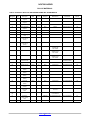
Table 3. PIN FUNCTION DESCRIPTION
Connector
Power
Pin Number
Terminal Name
Description
J1, VBAT
VBAT
Power Supply Input Voltage (14 V)
J2, GND
GND
Ground
J3
RSTOP
Programmable DC Current
J4
RTAIL
Programmable Duty Cycle
J5
DIAG
DIAG Open Drain Output
J6
J7
J8
J9
J10
J11
J12
J13
OUT1
OUT2
OUT3
OUT4
OUT5
OUT6
OUT7
OUT8
Current Outputs
J14
BALLAST IN
J15
J15
Connection to Top of the FB Resistor Network or Open Circuit
J16
J16
Connection to Short FB Pin to Ground or Open Circuit
J17
J17
Connection for Ballast Drive Gate Pin to Ballast Gate or to Ground
J18
BALLAST OUT
Connect when Using External Ballast Transistor.
Connects Drain of External Ballast Transistor to VSTRING.
Connect when Not Using External Ballast Transistor. Shorts S-D of External Transistor.
User Interface Locations
This lists all the user options available on the evaluation
board.
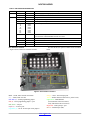
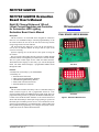
Figure 5 shows all the user interface locations.
Figure 5. User Interface Locations
Black − STOP, TAIL external connections.
Grey – STOP, TAIL switches.
Dark Blue (2) – STOP programming jumper.
Red (2) – TAIL programming jumper + post.
Dark Green – VP post.
Purple (2) – VSTRING post.
Light Blue (4) – OUT1−OUT8 open circuit jumpers.
Orange − OUT1−OUT8 output posts.
Yellow – Ballast Transistor Selection (2 yellow boxes).
Light Green – DIAG RESET.
(Not functional in the NCV7681A)
(Only functional in the NCV7681L)
Bright Red – DIAG jumper / post.
Brown – Feedback post (FB).
www.onsemi.com
4