1
TECHNICAL BULLETIN
[Issue No.] FA-A-0001-F
[Page] 1/58
[Title] Method of replacing High Performance model QCPU with Universal model QCPU
[Date of Issue] January 2008 (Ver. F: July 2011)
[Relevant Models] Q02UCPU, Q03UDCPU, Q04UDHCPU, Q06UDHCPU, Q10UDHCPU,
Q13UDHCPU, Q20UDHCPU, Q26UDHCPU, Q03UDECPU,
Q04UDEHCPU, Q06UDEHCPU, Q10UDEHCPU, Q13UDEHCPU,
Q20UDEHCPU, Q26UDEHCPU
Thank you for your continued support of Mitsubishi programmable controllers, MELSEC-Q series.
This bulletin provides detailed information on how to replace the High Performance model QCPU with the Universal model
QCPU.
For the method of replacing the Basic model QCPU with the Universal model QCPU, refer to the latest version of the technical
bulletin “FA-A-0054”.
Note that the reference manuals or the references described in this bulletin are information as of July 2011.
Contents
GENERIC TERMS ................................................................................................................................................................. 1
1. PRECAUTIONS FOR REPLACEMENT......................................................................................................................... 2
2. APPLICABLE PRODUCTS AND SOFTWARE............................................................................................................. 8
3. INSTRUCTIONS ............................................................................................................................................................... 11
3.1 Instructions not Supported in the Universal Model QCPU and Replacing Methods .................................................. 11
3.2 Replacing Programs Using Multiple CPU Transmission Dedicated Instructions ....................................................... 12
3.3 Program Replacement Examples.................................................................................................................................. 13
4. FUNCTIONS...................................................................................................................................................................... 29
4.1 Floating-point Operation Instructions .......................................................................................................................... 29
4.2 Error Check Processing for Floating-point Data Comparison Instructions ................................................................. 36
4.3 Range Check Processing for Index-modified Devices................................................................................................. 40
4.4 Device Latch Function ................................................................................................................................................. 43
4.5 File Usability Setting ................................................................................................................................................... 45
4.6 Parameter-valid Drive and Boot File Setting .............................................................................................................. 48
4.7 External Input/Output Forced On/Off Function........................................................................................................... 51
5. SPECIAL RELAY AND SPECIAL REGISTER.............................................................................................................. 55
5.1 Special Relay List ......................................................................................................................................................... 55
5.2 Special Register List..................................................................................................................................................... 57
REVISIONS ............................................................................................................................................................................ 58
GENERIC TERMS
Generic term
Description
Universal model QCPU
Generic term for Q02UCPU, Q03UDCPU, Q04UDHCPU, Q06UDHCPU, Q10UDHCPU,
Q13UDHCPU, Q20UDHCPU, Q26UDHCPU, Q03UDECPU, Q04UDEHCPU, Q06UDEHCPU,
Q10UDEHCPU, Q13UDEHCPU, Q20UDEHCPU, and Q26UDEHCPU
Built-in Ethernet port QCPU
Generic term for Q03UDECPU, Q04UDEHCPU, Q06UDEHCPU, Q10UDEHCPU,
Q13UDEHCPU, Q20UDEHCPU, and Q26UDEHCPU
QnUD(H)CPU
Generic term for Q03UDCPU, Q04UDHCPU, Q06UDHCPU, Q10UDHCPU, Q13UDHCPU,
Q20UDHCPU, and Q26UDHCPU
HEAD OFFICE : TOKYO BUILDING, 2-7-3 MARUNOUCHI, CHIYODA-KU, TOKYO 100-8310, JAPAN
NAGOYA WORKS : 1-14, YADA-MINAMI 5-CHOME, HIGASHI-KU, NAGOYA, JAPAN
TECHNICAL BULLETIN
[Issue No.] FA-A-0001-F
[Page] 2/58
[Title] Method of replacing High Performance model QCPU with Universal model QCPU
[Date of Issue] January 2008 (Ver. F: July 2011)
[Relevant Models] Q02UCPU, Q03UDCPU, Q04UDHCPU, Q06UDHCPU, Q10UDHCPU,
Q13UDHCPU, Q20UDHCPU, Q26UDHCPU, Q03UDECPU,
Q04UDEHCPU, Q06UDEHCPU, Q10UDEHCPU, Q13UDEHCPU,
Q20UDEHCPU, Q26UDEHCPU
1. PRECAUTIONS FOR REPLACEMENT
This chapter describes the precautions for replacing the High Performance model QCPU with the Universal model QCPU and
the replacement methods.
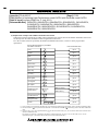
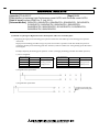
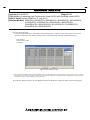
(1) System configuration
Table 1.1 Precautions and replacement methods
Item
Use of AnS/A series
module
GOT
Programming tool
connection
Applicable products
and software
Precaution
AnS/A series modules are not supported.
Replacement method
Use Q series modules.
GOT900 series cannot be connected.
Applicable USB cables are different.
y High Performance model QCPU
… A-B type
y Universal model QCPU
… A-miniB type
Products and software compatible with
the Universal model QCPU must be used.
Use GOT1000 series.
Use USB cables of A-miniB type. Or, use USB
conversion adapters of B-miniB type.
To configure a multiple CPU system,
CPU modules compatible with the
Universal model QCPU must be used.
In a multiple CPU system using the
Multiple CPU system
Motion CPU, an existing auto refresh area
and user setting area cannot be used for
data communication with the Motion
CPU.
In a redundant power supply system using
the Q38RB redundant power supply main
base unit and the Q68RB redundant
power supply extension base unit, the
Redundant power
status of the power supply module cannot
*1
supply system
be stored in the special relays and special
registers (SM1780 to SM1783/SD1780 to
SD1783). The status cannot be displayed
on the system monitor.
The simple dual-structured network
function is not supported.
MELSECNET/H
Reference
-
-
Products need to be replaced for the compatibility
with the Universal model QCPU and software need
to be upgraded for the communication with the
Universal model QCPU are described in Chapter 2.
CPU modules compatible with the Universal model
QCPU are described in Chapter 2.
Chapter 2
Chapter 2
For data communication with the Motion CPU, use
an auto refresh area and user setting area in the
multiple CPU high-speed transmission area.
Chapter 4 in the QCPU User's
Manual (Multiple CPU System)
Check the status of the power supply module by the
LED on the front of the module.
Section 7.1 in the QCPU User's
Manual (Hardware Design,
Maintenance and Inspection)
-
*1: The serial number (first five digits) of the Universal model QCPU must be “10041” or earlier.
HEAD OFFICE : TOKYO BUILDING, 2-7-3 MARUNOUCHI, CHIYODA-KU, TOKYO 100-8310, JAPAN
NAGOYA WORKS : 1-14, YADA-MINAMI 5-CHOME, HIGASHI-KU, NAGOYA, JAPAN
Section 7.7 in the Q Corresponding
MELSECNET/H Network System
Reference Manual (PLC to PLC
network)
TECHNICAL BULLETIN
[Issue No.] FA-A-0001-F
[Page] 3/58
[Title] Method of replacing High Performance model QCPU with Universal model QCPU
[Date of Issue] January 2008 (Ver. F: July 2011)
[Relevant Models] Q02UCPU, Q03UDCPU, Q04UDHCPU, Q06UDHCPU, Q10UDHCPU,
Q13UDHCPU, Q20UDHCPU, Q26UDHCPU, Q03UDECPU,
Q04UDEHCPU, Q06UDEHCPU, Q10UDEHCPU, Q13UDEHCPU,
Q20UDEHCPU, Q26UDEHCPU
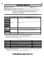
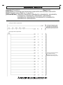
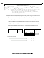
(2) Program
Table 1.2 Precautions and replacement methods
Item
Language and
instruction
Precaution
Replacement method
Replace the instructions not supported in the
Universal model QCPU are described in Chapter 3.
The Universal model QCPU performs Instructions for floating-point double-precision
program operations of floating-point data operation are added for the Universal model QCPU.
in single precision.
Replace the instructions if floating-point
double-precision operations are required, as
described in Section 4.1.
When using the floating-point data
When the floating-point data comparison
Floating-point
comparison instructions, LDE ,
instructions are used, modify the program as
operation
ANDE , ORE , LDED , ANDED ,
described in Section 4.2.
and ORED , if the comparison source
data are -0, nonnumeric, unnormalized
number, or ±∞, “OPERATION ERROR”
(error code: 4101) is detected. (
indicates one of the followings:
=, <>, <=, >=, <, >)
When a device number exceeds a setting Deselect the "Check device range at indexing"
range due to index modification,
checkbox in the PLC RAS tab of the PLC parameter
Device range check
“OPERATION ERROR” (error code:
dialog box so that checking is not performed.
at index modification
4101) is detected.
Program execution
type
Latch setting
Some instructions are not supported.
Reference
Chapter 3
y Appendix 4.4 in the QnUCPU
User's Manual (Function
Explanation, Program
Fundamentals)
y Section 4.1, 4.2
Section 3.17 in the QnUCPU
User's Manual (Function
Explanation, Program
Fundamentals)
y Section 4.3
Low-speed execution type programs are Use scan execution type programs or fixed scan
Section 2.10 in theQnUCPU User's
not supported.
execution type programs.
Manual (Function Explanation,
Program Fundamentals)
A program execution type cannot be
Use instructions for switching program execution
Section 2.10.5 in the QnUCPU
changed by remote operation.
types, such as PSTOP, POFF, and PSCAN.
User's Manual (Function
Explanation, Program
Fundamentals)
If latch ranges of internal user devices are The latch function of the Universal model QCPU is y Section 3.3 in the QnUCPU
specified, the processing time is added in enhanced.
User's Manual (Function
proportion to the device points set to be
(1) Large-capacity file register (R, ZR)
Explanation, Program
latched. (For example, if 8K points are
(2) Writing/reading device data to the standard
Fundamentals)
latched for the latch relay (L), the
ROM (SP.DEVST and S(P).DEVLD
y Section 4.4
processing time is 28.6μs.)
instructions)
(3) Latch range specification of internal devices
Change the latch method to the method described in
(1) to (3) above according to the application.
(To the next page)
HEAD OFFICE : TOKYO BUILDING, 2-7-3 MARUNOUCHI, CHIYODA-KU, TOKYO 100-8310, JAPAN
NAGOYA WORKS : 1-14, YADA-MINAMI 5-CHOME, HIGASHI-KU, NAGOYA, JAPAN
TECHNICAL BULLETIN
[Issue No.] FA-A-0001-F
[Page] 4/58
[Title] Method of replacing High Performance model QCPU with Universal model QCPU
[Date of Issue] January 2008 (Ver. F: July 2011)
[Relevant Models] Q02UCPU, Q03UDCPU, Q04UDHCPU, Q06UDHCPU, Q10UDHCPU,
Q13UDHCPU, Q20UDHCPU, Q26UDHCPU, Q03UDECPU,
Q04UDEHCPU, Q06UDEHCPU, Q10UDEHCPU, Q13UDEHCPU,
Q20UDEHCPU, Q26UDEHCPU
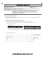
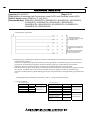
Table 1.2 Precautions and replacement methods (continued)
Item
Interrupt program
Precaution
The interrupt pointer (I49) for the
high-speed interrupt function is not
supported.
Interrupt counter is not supported.
The interrupt pointer (I32 to I40) for an
error is not supported.
When the SCJ instruction is used in the
Universal model QCPU, the AND
SM400 (or NOP instruction) needs to
SCJ instruction
be inserted immediately before the SCJ
instruction.
The number of index registers is
increased to 20 for the Universal model
ZPUSH instruction QCPU. The area for saving the data in
the index register with the ZPUSH
instruction is increased as well.
The following file usability setting for
each program is not available. *1
File usability setting
y File register
for each program
y Initial device value
y Comment
I/O refresh setting I/O refresh setting for each program is
for each program
not available.
Usage of a part of the special relay and
special register is different.
A sereis-compatible special relay and
special register are not supported.
SM/SD
(SM1000 to SM1255/SD1000 to
SD1255)
Replacement method
Reference
Consider the use of interrupt pointers for fixed scan
interrupt (I28 to I31).
Section 3.13.2 and 4.2.11 in the
QnUCPU User's Manual (Function
Explanation, Program
Check the numbers of executions for interrupt programs Fundamentals)
on the Interrupt program monitor list screen of GX
Developer.
-
-
Insert the AND SM400 (or NOP instruction)
immediately before the SCJ instruction when the SCJ
instruction is used.
Section 6.5.1 in the MELSEC-Q/L
Programming Manual (Common
Instruction)
Increase the save areas used for the ZPUSH instruction
as needed.
Section 7.18.8 in the
MELSEC-Q/L Programming
Manual (Common Instruction)
When file usability is set, modify the program as
described in Section 4.5.
y Section 2.10 in the QnUCPU
User's Manual (Function
Explanation, Program
Fundamentals)
y Section 4.5
MELSEC-Q/L Programming
Manual (Common Instruction)
Chapter 5
Use the RFS instruction if I/O refresh setting for each
program is required.
Replace the corresponding special relay and special
register as described in Chapter 5.
Using GX Developer, A series-compatible special relay Appendix 2 and Appendix 3 in the
and special register can be replaced with the Universal QCPU User's Manual (Hardware
model QCPU-compatible special relay and special
Design, Maintenance and
register. Note, however, that the ones which are not
Inspection)
compatible with the Universal model QCPU are replaced
with SM1255 and SD1255. Modify programs as needed.
Scan time and other processing times
Modify programs as needed, checking the processing
Processing time
are different.
timing.
*1: The local device file usability setting is also not available for the Q02UCPU, Q03UDCPU, Q04UDHCPU, and Q06UDHCPU if the serial number (first
five digits) is "10011" or earlier.
HEAD OFFICE : TOKYO BUILDING, 2-7-3 MARUNOUCHI, CHIYODA-KU, TOKYO 100-8310, JAPAN
NAGOYA WORKS : 1-14, YADA-MINAMI 5-CHOME, HIGASHI-KU, NAGOYA, JAPAN
TECHNICAL BULLETIN
[Issue No.] FA-A-0001-F
[Page] 5/58
[Title] Method of replacing High Performance model QCPU with Universal model QCPU
[Date of Issue] January 2008 (Ver. F: July 2011)
[Relevant Models] Q02UCPU, Q03UDCPU, Q04UDHCPU, Q06UDHCPU, Q10UDHCPU,
Q13UDHCPU, Q20UDHCPU, Q26UDHCPU, Q03UDECPU,
Q04UDEHCPU, Q06UDEHCPU, Q10UDEHCPU, Q13UDEHCPU,
Q20UDEHCPU, Q26UDEHCPU
(3) Drive and file
Table 1.3 Precautions and replacement methods
Item
Precaution
Replacement method
Files in the standard ROM cannot be
booted to the program memory.
Boot file setting
Booting operation is different.
Automatic all data
write from memory
card to standard
ROM
The setting method of this function is
different.
Since the Universal model QCPU holds the data in the
program memory even when the battery voltage
drops, the boot file setting is not necessary.
Move files with the boot setting (from the standard
ROM to the program memory) to the program
memory.
Replacement method when the parameter-valid drive
and the boot file setting are set in the High
Performance model QCPU is described in Section 4.6.
In the Boot file tab of the PLC parameter dialog box,
select "standard ROM" for the transfer destination.
Note, however, that the transfer destination of
"program" is fixed to "program memory". (Setting by
DIP switches is not necessary.)
Reference
y Section 2.1.2 in the QnUCPU
User's Manual (Function
Explanation, Program
Fundamentals)
y Section 4.6
Section 2.11 in the QnUCPU User's
Manual (Function Explanation,
Program Fundamentals)
(4) External communication
Table 1.4 Precautions and replacement methods
Item
Precaution
Replacement method
Module service
interval time read
Reference
The module service interval time cannot
be read.
The following frame types cannot be used Use the frame types below.
MELSEC-Q/L MELSEC
when accessing the Universal model
Communication Protocol Reference
y QnA-compatible 2C/3C/4C frame
QCPU. *1
Manual
y QnA-compatible 3E frame
y A-compatible 1C frame
y 4E frame
y A-compatible 1E frame
The following commands cannot specify
monitoring conditions.
MC protocol
y Randomly reading data in units of
word (Command: 0403)
y Device memory monitoring
(Command: 0801)
The applicable frame types are as follows:
y QnA-compatible 3C/4C frame
y QnA-compatible 3E frame
y 4E frame
*1: Applicable to the Q02UCPU, Q03UDCPU, Q04UDHCPU, Q06UDHCPU, Q13UDHCPU, and Q26UDHCPU if the serial number (first five digits) is
"10101" or earlier.
HEAD OFFICE : TOKYO BUILDING, 2-7-3 MARUNOUCHI, CHIYODA-KU, TOKYO 100-8310, JAPAN
NAGOYA WORKS : 1-14, YADA-MINAMI 5-CHOME, HIGASHI-KU, NAGOYA, JAPAN
TECHNICAL BULLETIN
[Issue No.] FA-A-0001-F
[Page] 6/58
[Title] Method of replacing High Performance model QCPU with Universal model QCPU
[Date of Issue] January 2008 (Ver. F: July 2011)
[Relevant Models] Q02UCPU, Q03UDCPU, Q04UDHCPU, Q06UDHCPU, Q10UDHCPU,
Q13UDHCPU, Q20UDHCPU, Q26UDHCPU, Q03UDECPU,
Q04UDEHCPU, Q06UDEHCPU, Q10UDEHCPU, Q13UDEHCPU,
Q20UDEHCPU, Q26UDEHCPU
(5) Diagnostic function
Table 1.5 Precautions and replacement methods
Item
Precaution
Replacement method
Error history
Error history data cannot be stored in the
memory card.
LED indication
priority setting
LED indication priority cannot be set.
Only LED indication setting at error
occurrence is supported.
The Universal model QCPU stores all storable data
(up to 100) in the built-in memory.
-
Reference
Section 3.18 in the QnUCPU User's
Manual (Function Explanation,
Program Fundamentals)
Section 3.20.2 in the QnUCPU
User's Manual (Function
Explanation, Program
Fundamentals)
(6) Debugging
Table 1.6 Precautions and replacement methods
Item
Monitor *3
Precaution
Replacement method
The monitoring condition cannot be Use the sampling trace function for checking device data
set.
under the specified monitoring condition. With this
function, changes of the specified device data can be
recorded at the following timings:
y at the execution of the specified step
y at the rising/falling edge of bit devices
y when the value of word devices coincide with the
setting value
y at every specified time
(settable range: 1ms to 5000ms)
Time required for executing a part Calculate the time using instruction processing time
of the program cannot be measured described in the manual.
using the scan time measurement
function.*1
Reference
Section 3.11.1 and 3.14 in the QnU
CPU User's Manual (Function
Explanation, Program Fundamentals)
y Section 3.13.3 in the QnUCPU
User's Manual (Function
Explanation, Program
Scan time
Fundamentals)
measurement by GX
Developer *3
y Appendix 1.4 in the MELSEC-Q/L
Programming Manual (Common
Instruction)
The external input/output forced
The function can be replaced with the programs
y Section 3.11.3 in the QnUCPU
on/off function is not supported. *2 described in Section 4.7.
User's Manual (Function
Explanation, Program
Note, however, that replacement method described does
not apply in the following cases:
Fundamentals)
External input/output
y Input and output targeted for forced on/off are
y Section 4.7
*3
forced on/off
referred to or changed using the direct input device
(DX) and direct output device (DY).
y Input and output targeted for forced on/off are
referred to or changed within an interrupt program.
*1: Scan time of each program can be checked on the Program monitor list screen.
*2: Device test by GX Developer can be performed.
*3: Applicable to the Q02UCPU, Q03UDCPU, Q04UDHCPU, Q06UDHCPU, Q13UDHCPU, and Q26UDHCPU if the serial number (first five digits) if
"10041" or earlier.
HEAD OFFICE : TOKYO BUILDING, 2-7-3 MARUNOUCHI, CHIYODA-KU, TOKYO 100-8310, JAPAN
NAGOYA WORKS : 1-14, YADA-MINAMI 5-CHOME, HIGASHI-KU, NAGOYA, JAPAN
TECHNICAL BULLETIN
[Issue No.] FA-A-0001-F
[Page] 7/58
[Title] Method of replacing High Performance model QCPU with Universal model QCPU
[Date of Issue] January 2008 (Ver. F: July 2011)
[Relevant Models] Q02UCPU, Q03UDCPU, Q04UDHCPU, Q06UDHCPU, Q10UDHCPU,
Q13UDHCPU, Q20UDHCPU, Q26UDHCPU, Q03UDECPU,
Q04UDEHCPU, Q06UDEHCPU, Q10UDEHCPU, Q13UDEHCPU,
Q20UDEHCPU, Q26UDEHCPU
(7) Switch on the front of the CPU module
Table 1.7 Precautions and replacement methods
Item
Precaution
Replacement method
Reference
Section 6.1.3 in the QCPU User's
Manual (Hardware Design,
Maintenance and Inspection)
Section 6.1.3 in the QCPU User's
Manual (Hardware Design,
Maintenance and Inspection)
Switch on the front of The system protect cannot be set by Data in the files can be protected by setting a password Section 3.19 in the QnUCPU User's
the CPU module
Manual (Function Explanation,
the switch.
for each file. Password for each file can be registered
Program Fundamentals)
with GX Developer.
The parameter-valid drive setting is The Universal model QCPU automatically determines
y Section 6.1.3 in the QCPU User's
Manual (Hardware Design,
not necessary.
the parameter-valid drive.
Maintenance and Inspection)
Change the setting as described in Section 4.6 when the
parameter-valid drive is set to other than the program
y Section 4.6
memory in the High Performance model QCPU.
The operation method with the
RESET/RUN/STOP switch is
modified.
Latch data cannot be cleared by the
switch.
The RESET/STOP/RUN switch of the Universal model
QCPU can be used for the reset operation of the CPU
module and switching between STOP and RUN status.
To clear latch data, use the remote latch clear operation
of GX Developer.
HEAD OFFICE : TOKYO BUILDING, 2-7-3 MARUNOUCHI, CHIYODA-KU, TOKYO 100-8310, JAPAN
NAGOYA WORKS : 1-14, YADA-MINAMI 5-CHOME, HIGASHI-KU, NAGOYA, JAPAN
TECHNICAL BULLETIN
[Issue No.] FA-A-0001-F
[Page] 8/58
[Title] Method of replacing High Performance model QCPU with Universal model QCPU
[Date of Issue] January 2008 (Ver. F: July 2011)
[Relevant Models] Q02UCPU, Q03UDCPU, Q04UDHCPU, Q06UDHCPU, Q10UDHCPU,
Q13UDHCPU, Q20UDHCPU, Q26UDHCPU, Q03UDECPU,
Q04UDEHCPU, Q06UDEHCPU, Q10UDEHCPU, Q13UDEHCPU,
Q20UDEHCPU, Q26UDEHCPU
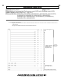
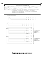
(8) SFC
Table 1.8 Precautions and replacement methods
Item
Step transition
monitoring timer
SFC operation mode
setting
SFC program for
program execution
management
SFC control
instruction
Precaution
Replacement method
The step transition monitoring timer is not Change the program as described in Appendix 3.1 in
supported.
the MELSEC-Q/L/QnA Programming Manual
(SFC)
The periodic execution block setting is
Change the program as described in Appendix 3.2 in
not supported.
the MELSEC-Q/L/QnA Programming Manual
(SFC)
An operation mode at double block
START cannot be selected. (Fixed to
“WAIT”.)*1
An operation mode at transition to active
step cannot be selected. (Fixed to
“TRANSFER".)
SFC programs for program execution
management are not supported.
Some SFC control instructions are not
supported.
SFC control instructions not supported in the
Universal model QCPU and replacing methods are
described in Section 3.1.
Reference
Section 4.6 and Appendix 3.1 in the
MELSEC-Q/L/QnA Programming
Manual (SFC)
Section 4.7.4 and Appendix 3.2 in
the MELSEC-Q/L/QnA
Programming Manual (SFC)
Section 4.7.5 in the
MELSEC-Q/L/QnA Programming
Manual (SFC)
Section 4.7.6 in the
MELSEC-Q/L/QnA Programming
Manual (SFC)
Section 5.2.3 in the
MELSEC-Q/L/QnA Programming
Manual (SFC)
y Section 4.4 in the
MELSEC-Q/L/QnA
Programming Manual (SFC)
y Section 3.1
Section 4.8 in the
MELSEC-Q/L/QnA Programming
Manual (SFC)
The following SFC comment readout
instructions are not supported.
SFC comment
y S(P).SFCSCOMR (SFC step comment
readout instruction*1
readout instruction)
y S(P).SFCTCOMR (SFC transition
condition comment readout instruction)
SFC program files cannot be written to
Section 6.6 in the
y Write program data to the CPU module after
the running CPU module. (Programs in
changing the Universal model QCPU status to
MELSEC-Q/L/QnA Programming
Method of SFC
SFC Figure can be changed online.)
STOP.
Manual (SFC)
program change
y An inactive block in an SFC program can be
changed by online change of inactive block.*2
*1: This applies to the Universal model QCPU whose serial number (first five digits) is "12051" or earlier.
*2: This operation is available for the Universal model QCPU other than the Q02UCPU and whose serial number (first five digits) is "12052" or later.
HEAD OFFICE : TOKYO BUILDING, 2-7-3 MARUNOUCHI, CHIYODA-KU, TOKYO 100-8310, JAPAN
NAGOYA WORKS : 1-14, YADA-MINAMI 5-CHOME, HIGASHI-KU, NAGOYA, JAPAN
TECHNICAL BULLETIN
[Issue No.] FA-A-0001-F
[Page] 9/58
[Title] Method of replacing High Performance model QCPU with Universal model QCPU
[Date of Issue] January 2008 (Ver. F: July 2011)
[Relevant Models] Q02UCPU, Q03UDCPU, Q04UDHCPU, Q06UDHCPU, Q10UDHCPU,
Q13UDHCPU, Q20UDHCPU, Q26UDHCPU, Q03UDECPU,
Q04UDEHCPU, Q06UDEHCPU, Q10UDEHCPU, Q13UDEHCPU,
Q20UDEHCPU, Q26UDEHCPU
2. APPLICABLE PRODUCTS AND SOFTWARE
(1) Products need to be replaced for the compatibility with the Universal model QCPU
The following tables show products need to be replaced for the compatibility with the Universal model QCPU. (As for
devices not listed in the tables below, replacement is not required.)
Table 2.1 Product need to be replaced (Communication modules)
Product
Model
Serial number (first five digits) of the product compatible with the Universal model QCPU *2
Used with
Used with Q10UDH/Q13UDH/Q20UDH/Q26UDHCPU
Q02U/Q03UD/Q04UDH/Q06UDHCPU
or Built-in Ethernet port QCPU
Web server module *1 y QJ71WS96
"09042" or later.
"10012" or later.
MES interface module y QJ71MES96
*1: The Universal model QCPU does not operate normally when the Web server module on which GX RemoteService-I is installed is used.
*2: The Universal model QCPU does not operate normally when an incompatible module version is used.
Table 2.2 Product need to be replaced (Personal computer boards)
Product
Dedicated software package version compatible with the Universal model QCPU *1
Used with Q10UDH/
Used with
Used with
Q20UDHCPU, or Built-in
Q02U/Q03UD/Q04UDH/
Q13UDH/Q26UDHCPU
Ethernet port QCPU
Q06UDHCPU
Model
CC-Link IE controller network
interface board
y Q80BD-J71GP21-SX
y Q80BD-J71GP21S-SX
y Q80BD-J71LP21-25
SI/QSI/H-PCF
y Q80BD-J71LP21S-25
MELSECNET/H optical cable
y Q81BD-J71LP21-25
interface board
GI optical cable y Q80BD-J71LP21G
Coaxial cable
y Q80BD-J71BR11
CC-Link system master/local
y Q80BD-J61BT11N
interface board
y Q81BD-J61BT11
*1: No restrictions on the board itself.
No restrictions
Version 1.03D or later
Version 15R or later
Version 18U or later
Version 19V or later
Version 19V or later
Version 15R or later
Version 18U or later
Version 1.02C or later
Version 1.06G or later
Version 1.05F or later
Version 1.06G or later
Version 1.06G or later
Version 20W or later
Version 1.07H or later
Table 2.3 Product need to be replaced (GOT)
Product
GOT1000
Model
GT Designer2 OS version compatible with the Universal model QCPU *1
Used with Q03UDE/
Used with
Used with
Used with Q02U/
Q04UDEH/Q06UDEH/
Q10UDH/
Q13UDH/
Q03UD/Q04UDH/
Q13UDEH/Q26UDEHCPU
Q20UDHCPU
Q26UDHCPU
Q06UDHCPU
Used with
Q10UDEH/
Q20UDEHCPU
y GT15 y GT11 -
Version 2.60N
or later
Version 2.76E
or later
Version 2.91V
or later
Version 2.81K
or later
Version 2.91V
or later
y GT10 -
Version 2.76E
or later
Version 2.76E
or later
Version 2.91V
or later
-
-
*1: No restrictions on GOT itself.
HEAD OFFICE : TOKYO BUILDING, 2-7-3 MARUNOUCHI, CHIYODA-KU, TOKYO 100-8310, JAPAN
NAGOYA WORKS : 1-14, YADA-MINAMI 5-CHOME, HIGASHI-KU, NAGOYA, JAPAN
TECHNICAL BULLETIN
[Issue No.] FA-A-0001-F
[Page] 10/58
[Title] Method of replacing High Performance model QCPU with Universal model QCPU
[Date of Issue] January 2008 (Ver. F: July 2011)
[Relevant Models] Q02UCPU, Q03UDCPU, Q04UDHCPU, Q06UDHCPU, Q10UDHCPU,
Q13UDHCPU, Q20UDHCPU, Q26UDHCPU, Q03UDECPU,
Q04UDEHCPU, Q06UDEHCPU, Q10UDEHCPU, Q13UDEHCPU,
Q20UDEHCPU, Q26UDEHCPU
Table 2.4 Product need to be replaced (Network module and serial communication module)
Module version compatible with the Universal model QCPU
Product
Model
y QJ71LP21-25
y QJ71LP21S-25
MELSECNET/H module
y QJ71LP21G
y QJ71BR11
y QJ71C24N
Serial communication
y QJ71C24N-R2
module
y QJ71C24N-R4
Modem interface
module
Used with Q02U/Q03UD/ 04UDH/Q06UDH/
Q10UDH/Q13UDH/Q20UDH/Q26UDHCPU
Used with Built-in Ethernet port QCPU
Some restrictions depending on use conditions *1
No restrictions
The serial number (first five digits)
"10042" or later.
y QJ71CMON
*1: The serial number (first five digits) of the MELSECNET/H module must be "10042" or later if all conditions 1) to 4) described below are satisfied.
1) A multiple CPU system including Built-in Ethernet port QCPU is configured.
2) GX Developer or GOT is connected to an Ethernet port of Built-in Ethernet port QCPU.
3) GX Developer or GOT accesses the CPU module on another station via the MELSECNET/H module controlled by another CPU.
4) The access target on another station is A/QnA series CPU module.
HEAD OFFICE : TOKYO BUILDING, 2-7-3 MARUNOUCHI, CHIYODA-KU, TOKYO 100-8310, JAPAN
NAGOYA WORKS : 1-14, YADA-MINAMI 5-CHOME, HIGASHI-KU, NAGOYA, JAPAN
TECHNICAL BULLETIN
[Issue No.] FA-A-0001-F
[Page] 11/58
[Title] Method of replacing High Performance model QCPU with Universal model QCPU
[Date of Issue] January 2008 (Ver. F: July 2011)
[Relevant Models] Q02UCPU, Q03UDCPU, Q04UDHCPU, Q06UDHCPU, Q10UDHCPU,
Q13UDHCPU, Q20UDHCPU, Q26UDHCPU, Q03UDECPU,
Q04UDEHCPU, Q06UDEHCPU, Q10UDEHCPU, Q13UDEHCPU,
Q20UDEHCPU, Q26UDEHCPU
(2) CPU modules that can configure a multiple CPU system with the Universal model QCPU
CPU modules that can configure a multiple CPU system with the Universal model QCPU are shown below.
(a) For the QnUD(H)CPU or Built-in Ethernet port QCPU
Table 2.5 CPU module that can configure a multiple CPU system with the QnUD(H)CPU or Built-in Ethernet port QCPU
CPU module
Configured with
03UD/Q04UDH/
Q06UDHCPU
Model
Motion CPU
y Q172DCPU
y Q173DCPU
PC CPU
module
y PPC-CPU852(MS)
C Controller
module
High
Performance
model QCPU
Process CPU
Applicable version
Configured with Q13UDH/
Q26UDH/Q03UDE/
Q04UDEH/Q06UDEH/
Q13UDEH/Q26UDEHCPU
Configured with
Q10UDH/ Q20UDH/
Q10UDEH/
Q20UDEHCPU
Use the multiple CPU
high-speed main base unit
(Q3 DB) for a main base unit.
No restrictions
y Q06CCPU-V
y Q06CCPU-V-B
y Q12DCCPU-V
y Q02CPU
y Q02HCPU
y Q06HCPU
y Q12HCPU
y Q25HCPU
y Q02PHCPU
y Q06PHCPU
y Q12PHCPU
y Q25PHCPU
Driver S/W
(PPC-DRV-02)
version 1.01 or later
No restrictions
Driver S/W
(PPC-DRV-02)
version 1.02 or later
Restrictions
Driver S/W
(PPC-DRV-02)
version 1.03 or later
-
Serial number (first five digits) "10102" or later.
-
No restrictions
-
Function version B or later
-
No restrictions
-
(b) For the Q02UCPU
Table 2.6 CPU module that can configure a multiple CPU system with Q02UCPU
CPU module
Motion CPU
PC CPU module
C Controller module
Model
y Q172CPUN(-T)
y Q173CPUN(-T)
y Q172HCPU(-T)
y Q173HCPU(-T)
y PPC-CPU852(MS)
y Q06CCPU-V
y Q06CCPU-V-B
Applicable version
Restrictions
No restrictions
The multiple CPU high-speed main base
unit (Q3 DB) cannot be used for a main
base unit.
Driver S/W (PPC-DRV-02) version 1.01 or later.
-
Serial number (first five digits) "10102" or later.
-
HEAD OFFICE : TOKYO BUILDING, 2-7-3 MARUNOUCHI, CHIYODA-KU, TOKYO 100-8310, JAPAN
NAGOYA WORKS : 1-14, YADA-MINAMI 5-CHOME, HIGASHI-KU, NAGOYA, JAPAN
TECHNICAL BULLETIN
[Issue No.] FA-A-0001-F
[Page] 12/58
[Title] Method of replacing High Performance model QCPU with Universal model QCPU
[Date of Issue] January 2008 (Ver. F: July 2011)
[Relevant Models] Q02UCPU, Q03UDCPU, Q04UDHCPU, Q06UDHCPU, Q10UDHCPU,
Q13UDHCPU, Q20UDHCPU, Q26UDHCPU, Q03UDECPU,
Q04UDEHCPU, Q06UDEHCPU, Q10UDEHCPU, Q13UDEHCPU,
Q20UDEHCPU, Q26UDEHCPU
(3) Software need to be upgraded for the compatibility with the Universal model QCPU
The following table shows software need to be upgraded for the communication with the Universal model QCPU. (As for
software not listed in the table below, version upgrade is not required.)
The latest version can be downloaded from the MELFANSweb.
Table 2.7 Software need to be upgraded for the compatibility with the Universal model QCPU
Software
Version compatible with the Universal model QCPU
Used with Q03UDE/
Used with Q13UDH/
Q04UDEH/Q06UDEH,
Q26UDHCPU
Q13UDEH/Q26UDEHCPU
Used with Q02U/
Q03UD/Q04UDH/
Q06UDHCPU
Model
Used with Q10UDH/
Q20UDH/Q10UDEH/
Q20UDEHCPU
Version 8.48A or later
Version 8.62Q or later
Version 8.68W or later
Version 8.78G or later
GX Configulator-AD SW2D5C-QADU-E
Version 2.05F or later *1
Version 2.05F or later *2
Version 2.05F or later *3
Version 2.05F or later *4
GX Configulator-DA SW2D5C-QDAU-E
Version 2.06G or later *1
Version 2.06G or later *2
Version 2.06G or later *3
Version 2.06G or later *4
GX Configulator-SC SW2D5C-QSCU-E
Version 2.12N or later *1
Version 2.12N or later *2
Version 2.17T or later *3
Version 2.17T or later *4
GX Developer
SW8D5C-GPPW-E
*1
*2
GX Configulator-CT SW0D5C-QCTU-E Version 1.25AB or later Version 1.25AB or later
*1
*2
GX Configulator-TI SW1D5C-QTIU-E Version 1.24AA or later Version 1.24AA or later
GX Configulator-TC SW0D5C-QTCU-E
GX Configulator-FL SW0D5C-QFLU-E
Version 1.23Z or later
*1
Version 1.23Z or later
*1
Version 1.23Z or later
*2
Version 1.23Z or later
*2
Version 1.25AB or later
*3
Version 1.25AB or later *4
Version 1.24AA or later
*3
Version 1.24AA or later *4
Version 1.23Z or later
*3
Version 1.23Z or later *4
Version 1.23Z or later
*3
Version 1.23Z or later *4
Version 2.30G or later
*5
Version 2.32J or later
GX Configulator-QP SW2D5C-QD75P-E
Version 2.25B or later
Version 2.29F or later
GX Configulator-PT SW1D5C-QPTU-E
Version 1.23Z or later *1
Version 1.23Z or later *2
Version 1.23Z or later *3
Version 1.23Z or later *4
GX Configulator-AS SW1D5C-QASU-E
Version 1.21X or later *1
Version 1.21X or later *2
Version 1.21X or later *3
Version 1.21X or later *4
GX Configulator-MB SW1D5C-QMBU-E
Version 1.08J or later *1
Version 1.08J or later *2
Version 1.08J or later *3
Version 1.08J or later *4
GX Configulator-DN SW1D5C-QDNU-E
*1
*2
Version 1.23Z or later
Version 1.23Z or later
Version 3.09K or later
Version 3.10L or later
SW3D5C-ACT-E
SW7D5C-LLT-E
Version 7.23Z or later *4 Version 7.23Z or later *4
GX Simulator
*1: The software can be used by installing GX Developer Version 8.48A or later.
*2: The software can be used by installing GX Developer Version 8.62Q or later.
*3: The software can be used by installing GX Developer Version 8.68W or later.
*4: The software can be used by installing GX Developer Version 8.78G or later.
*5: GX Configurator-QP Version 2.29F can be used when connected via USB.
MX Component
Version 1.24AA or later
Version 3.11M or later
Version 3.12N or later
Version 7.23Z or later *4
Table 2.8 Software not supported by the Universal model QCPU
Product
Model
SW D5C-EXP-E
GX Converter
SW D5C-CNVW-E
Version 1.24AA or later *4
Version 7.23Z or later *4
(4) Software not supported by the Universal model QCPU
The following table shows software not supported by the Universal model QCPU.
GX Explorer
*3
HEAD OFFICE : TOKYO BUILDING, 2-7-3 MARUNOUCHI, CHIYODA-KU, TOKYO 100-8310, JAPAN
NAGOYA WORKS : 1-14, YADA-MINAMI 5-CHOME, HIGASHI-KU, NAGOYA, JAPAN
TECHNICAL BULLETIN
[Issue No.] FA-A-0001-F
[Page] 13/58
[Title] Method of replacing High Performance model QCPU with Universal model QCPU
[Date of Issue] January 2008 (Ver. F: July 2011)
[Relevant Models] Q02UCPU, Q03UDCPU, Q04UDHCPU, Q06UDHCPU, Q10UDHCPU,
Q13UDHCPU, Q20UDHCPU, Q26UDHCPU, Q03UDECPU,
Q04UDEHCPU, Q06UDEHCPU, Q10UDEHCPU, Q13UDEHCPU,
Q20UDEHCPU, Q26UDEHCPU
3. INSTRUCTIONS
3.1 Instructions not Supported in the Universal Model QCPU and Replacing Methods
The Universal model QCPU does not support instructions listed in Table 3.1 and 3.2. Use alternative methods described in
the tables. (For other instructions, replacement is not required.)
Table 3.1 Instructions not supported in the Universal model QCPU and alternative methods
Symbol
IX
IXEND
Instruction
Index modification of entire ladder
Replacing method
Use alternative programs.
Reference
Section 3.3 (1)
IXSET
Modification value specification in
index modification of entire ladder
Section 3.3 (2)
Change the program so that the device offset values specified by the
IXSET instruction are directly set to the index modification table using
the MOV instruction.
PR
Print ASCII code instruction
y It is recommended to use GOT as an ASCII code display device. ASCII Section 3.3 (3)
codes stored in devices are directly displayed as characters on GOT.
y Instructions can be replaced using a replacement program.
PRC
Print comment instruction
y It is recommended to use GOT as an ASCII code display device.
Device comments can be displayed on GOT.
y Comment data can be output to a display device in the replacement
program of the PR instruction after reading data using the reading
device comment data instruction (COMRD(P)).
CHKST
Specific format failure check
instruction
Instructions can be replaced using a replacement program.
Format change instruction for CHK
instruction
Failure detection ladder patterns can be changed in a replacement
program.
PLOW
Program low-speed execution
registration instruction
y Use the PSCAN instruction instead of this instruction when low-speed
execution type programs are replaced with scan execution type
programs.
y No instruction can be used if low-speed execution type programs are
replaced with fixed scan execution type programs.
-
PCHK
Program execution status check
instruction
Check a program execution status on the Program monitor list screen of
GX Developer. For details, refer to Section 3.13.1 in the QnUCPU
User's Manual (Function Explanation, Program Fundamentals).
-
KEY
Numerical key input instruction
y It is recommended to use GOT as a numeral input device.
y Instructions can be replaced using a replacement program.
IXDEV
CHK
CHKCIR
CHKEND
PLOADP
Load program from memory card
PUNLOADP
Unload program from memory card
PSWAPP
Load + Unload
Store all programs to be executed in the program memory. The
Universal model QCPU can neither add programs to the program
memory nor change them with other programs during RUN.
If the capacity of the program memory is not enough, store parameters,
device comments, and device initial values in the program memory into
the standard ROM or memory card instead.
HEAD OFFICE : TOKYO BUILDING, 2-7-3 MARUNOUCHI, CHIYODA-KU, TOKYO 100-8310, JAPAN
NAGOYA WORKS : 1-14, YADA-MINAMI 5-CHOME, HIGASHI-KU, NAGOYA, JAPAN
Section 3.3 (4)
Section 3.3 (5)
-
TECHNICAL BULLETIN
[Issue No.] FA-A-0001-F
[Page] 14/58
[Title] Method of replacing High Performance model QCPU with Universal model QCPU
[Date of Issue] January 2008 (Ver. F: July 2011)
[Relevant Models] Q02UCPU, Q03UDCPU, Q04UDHCPU, Q06UDHCPU, Q10UDHCPU,
Q13UDHCPU, Q20UDHCPU, Q26UDHCPU, Q03UDECPU,
Q04UDEHCPU, Q06UDEHCPU, Q10UDEHCPU, Q13UDEHCPU,
Q20UDEHCPU, Q26UDEHCPU
Table 3.2 SFC control instructions not supported in the Universal model QCPU and alternative methods
Symbol
Instruction
Alternative method
LD TRn
AND TRn
OR TRn
LDI TRn
ANDI TRn
ORI TRn
LD BLm\TRn
AND BLm\TRn
OR BLm\TRn
LDI BLm\TRn
ANDI BLm\TRn
ORI BLm\TRn
Forced transition check
instruction
When the programmable controller type is changed, these instructions are converted into SM1255.
Modify programs as needed.
SCHG(D)
Active step change instruction
Refer to Appendix 3 "Restrictions on Basic Model QCPU, Universal Model QCPU, and LCPU and
Alternative Methods" in the MELSEC-Q/L/QnA Programming Manual (SFC).
SET
SET
RST
RST
Transition control instruction
Refer to Appendix 3 " Restrictions on Basic Model QCPU, Universal Model QCPU, and LCPU and
Alternative Methods" in the MELSEC-Q/L/QnA Programming Manual (SFC).
Block switching instruction
When the programmable controller type is changed, these instructions are converted into SM1255.
Modify programs as needed.
TRn
BLm\TRn
TRn
BLm\TRn
BRSET(S)
3.2 Replacing Programs Using Multiple CPU Transmission Dedicated Instructions
(1) Replacing the module with the QnUD(H)CPU or Built-in Ethernet port QCPU
Table 3.3 shows instructions need to be replaced and corresponding alternative instructions. For the specifications of each
instruction, refer to the manuals for the Motion CPU.
Table 3.3 Instructions need to be replaced
Symbol
S(P).DDWR
S(P).DDRD
S(P).SFCS
S(P).SVST
S(P).CHGA
S(P).CHGV
S(P).CHGT
S(P).GINT
Instruction description
Write other CPU device data into host CPU
Read other CPU device data into host CPU
Request of motion SFC program startup
Request of servo program startup
Current value change of halted axis/synchronized encoder/cam axis
Axis speed change during positioning and JOG operation
Torque control value change during operation and suspension in real mode
Request of other CPU interrupt program startup
Symbol of alternative instruction
D(P).DDWR
D(P).DDRD
D(P).SFCS
D(P).SVST
D(P).CHGA
D(P).CHGV
D(P).CHGT
D(P).GINT
(2) Replacing the module with the Q02UCPU
The Q02UCPU supports the same multiple CPU transmission dedicated instructions used in the Basic model QCPU.
The alternative instructions in Table 3.3 are not available for the Q02UCPU.
HEAD OFFICE : TOKYO BUILDING, 2-7-3 MARUNOUCHI, CHIYODA-KU, TOKYO 100-8310, JAPAN
NAGOYA WORKS : 1-14, YADA-MINAMI 5-CHOME, HIGASHI-KU, NAGOYA, JAPAN
TECHNICAL BULLETIN
[Issue No.] FA-A-0001-F
[Page] 15/58
[Title] Method of replacing High Performance model QCPU with Universal model QCPU
[Date of Issue] January 2008 (Ver. F: July 2011)
[Relevant Models] Q02UCPU, Q03UDCPU, Q04UDHCPU, Q06UDHCPU, Q10UDHCPU,
Q13UDHCPU, Q20UDHCPU, Q26UDHCPU, Q03UDECPU,
Q04UDEHCPU, Q06UDEHCPU, Q10UDEHCPU, Q13UDEHCPU,
Q20UDEHCPU, Q26UDEHCPU
3.3 Program Replacement Examples
This section shows program replacement examples for the instructions listed in Section 3.1. (Skip this section if instructions
listed in Section 3.1 are not used.)
(1) Replacement example of the IX and IXEND instructions
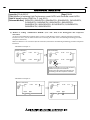
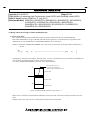
A replacement example of program using the IX and IXEND instructions is shown below.
To save index register data using the ZPUSH instruction, a 23-word index register save area is required.
(a) Example of device assignment
(Before replacement)
(After replacement)
Application
Index modification table
Device
D100 to D115
Application
Device
Index modification table
D100 to D115
Index register save area
D200 to D222
If the device numbers in the example above are used for other applications, assign unused device numbers instead.
(b) Program before replacement
The modification value set in the
index modification table is added.
Modification target
(No change required)
HEAD OFFICE : TOKYO BUILDING, 2-7-3 MARUNOUCHI, CHIYODA-KU, TOKYO 100-8310, JAPAN
NAGOYA WORKS : 1-14, YADA-MINAMI 5-CHOME, HIGASHI-KU, NAGOYA, JAPAN
TECHNICAL BULLETIN
[Issue No.] FA-A-0001-F
[Page] 16/58
[Title] Method of replacing High Performance model QCPU with Universal model QCPU
[Date of Issue] January 2008 (Ver. F: July 2011)
[Relevant Models] Q02UCPU, Q03UDCPU, Q04UDHCPU, Q06UDHCPU, Q10UDHCPU,
Q13UDHCPU, Q20UDHCPU, Q26UDHCPU, Q03UDECPU,
Q04UDEHCPU, Q06UDEHCPU, Q10UDEHCPU, Q13UDEHCPU,
Q20UDEHCPU, Q26UDEHCPU
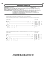
(c) Program after replacement
y Replace the IX instruction with the ZPUSH instruction and set the contents of index modification table in the to
index register.
y Replace the IXEND instruction with the ZPOP instruction.
Current index register is
saved.
Contents of the index
modification table are
set to the index
registers Z0 to Z15.
Transition
from the IX
instruction
Modification target
(No change required)
The saved index register is restored.
(Transition from the IXEND instruction)
HEAD OFFICE : TOKYO BUILDING, 2-7-3 MARUNOUCHI, CHIYODA-KU, TOKYO 100-8310, JAPAN
NAGOYA WORKS : 1-14, YADA-MINAMI 5-CHOME, HIGASHI-KU, NAGOYA, JAPAN
TECHNICAL BULLETIN
[Issue No.] FA-A-0001-F
[Page] 17/58
[Title] Method of replacing High Performance model QCPU with Universal model QCPU
[Date of Issue] January 2008 (Ver. F: July 2011)
[Relevant Models] Q02UCPU, Q03UDCPU, Q04UDHCPU, Q06UDHCPU, Q10UDHCPU,
Q13UDHCPU, Q20UDHCPU, Q26UDHCPU, Q03UDECPU,
Q04UDEHCPU, Q06UDEHCPU, Q10UDEHCPU, Q13UDEHCPU,
Q20UDEHCPU, Q26UDEHCPU
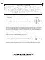
(2) Replacement example of the IXDEV and IXSET instructions
Change the program so that the device offset values specified for the contacts between the IXDEV and IXSET instructions
are directly set to the index modification table using the MOV instruction.
For a device offset value not specified by the IXDEV and IXSET instructions, it value to 0 in the program after
replacement.
Device offset specification by the INDEV
and IXSET instructions
Timer
Counter
Input *1
Output *1
Internal relay
Latch relay
Edge relay
Link relay *1
Data register
Link register *1
File register
Intelligent function
module device *2
Link direct device *3
File register
(through number)
Pointer
Index modification table
T
(D)+0
C
(D)+1
X
(D)+2
Y
(D)+3
M
(D)+4
L
(D)+5
V
(D)+6
B
(D)+7
D .XX
(D)+8
W .XX
(D)+9
R .XX
(D)+10
Start I/O number
(D)+11
Buffer memory
(D)+12
U \G .XX
J \B
(D)+13
ZR .XX
IXSET
(D)+14
P
(D)+15
*1: Device numbers are represented in hexadecimal. Use hexadecimal constants (H ) when setting values in the index modification table.
*2: Start I/O numbers (U ) are represented in hexadecimal. Use hexadecimal constants (H ) when setting values in the index modification
table.
*3: Devices B, W, X, or Y can be specified following J \. Set device numbers for B, W, X, and Y as device offset values of each device in
the index modification table.
For example, if ‘J10\Y220’ is specified by the IXDEV or IXSET instruction, set ‘K10’ in (D)+13 and ‘H220’ in (D)+3 in the
replacement program. ((D) indicates the start device in the index modification table.)
HEAD OFFICE : TOKYO BUILDING, 2-7-3 MARUNOUCHI, CHIYODA-KU, TOKYO 100-8310, JAPAN
NAGOYA WORKS : 1-14, YADA-MINAMI 5-CHOME, HIGASHI-KU, NAGOYA, JAPAN
TECHNICAL BULLETIN
[Issue No.] FA-A-0001-F
[Page] 18/58
[Title] Method of replacing High Performance model QCPU with Universal model QCPU
[Date of Issue] January 2008 (Ver. F: July 2011)
[Relevant Models] Q02UCPU, Q03UDCPU, Q04UDHCPU, Q06UDHCPU, Q10UDHCPU,
Q13UDHCPU, Q20UDHCPU, Q26UDHCPU, Q03UDECPU,
Q04UDEHCPU, Q06UDEHCPU, Q10UDEHCPU, Q13UDEHCPU,
Q20UDEHCPU, Q26UDEHCPU
(a) Program before replacement
The device offset values for input
(X), output (Y), internal relay (M),
data register (D), link register (W),
and pointer (P) are set to the index
modification table starting from D0.
(b) Program after replacement
The device offset values specified
by the IXDEV and IXSET
instructions are set to the index
modification table starting from D0.
HEAD OFFICE : TOKYO BUILDING, 2-7-3 MARUNOUCHI, CHIYODA-KU, TOKYO 100-8310, JAPAN
NAGOYA WORKS : 1-14, YADA-MINAMI 5-CHOME, HIGASHI-KU, NAGOYA, JAPAN
TECHNICAL BULLETIN
[Issue No.] FA-A-0001-F
[Page] 19/58
[Title] Method of replacing High Performance model QCPU with Universal model QCPU
[Date of Issue] January 2008 (Ver. F: July 2011)
[Relevant Models] Q02UCPU, Q03UDCPU, Q04UDHCPU, Q06UDHCPU, Q10UDHCPU,
Q13UDHCPU, Q20UDHCPU, Q26UDHCPU, Q03UDECPU,
Q04UDEHCPU, Q06UDEHCPU, Q10UDEHCPU, Q13UDEHCPU,
Q20UDEHCPU, Q26UDEHCPU
(3) Replacement example of the PR instruction
The number of output characters can be switched by the on/off status of SM701.
(a) Example of device assignment
(Before replacement)
Application
Output string
(After replacement)
Device
Application
Device
D0 to D3
Output string
D0 to D3
ASCII code output signal
Y100 to Y107
ASCII code output signal
Y100 to Y107
Strobe signal
Y108
Strobe signal
Y108
In-execution flag
Y109
In-execution flag
Y109
Output string storage address (BIN32)
D20 to D21
Output string storage address (BIN32)
(Used for sub-routine programs and interrupt
programs)
D200 to D201
Number of output characters
D202
Output module start Y number
D203
Character extraction position
D204
Number of extracted characters
D205
String output status value
D206
Result of string extraction by the MIDR
instruction
D207
String output in-execution flag
M200
For index modification
Z0
If the device numbers in the example above are used for other applications, assign unused device numbers instead.
(b) Program before replacement
The number of output strings is set
to variable. (Output untill ASCII code
00H appears.)
The strings stored in D0 or later are
output to Y100 to Y108.
HEAD OFFICE : TOKYO BUILDING, 2-7-3 MARUNOUCHI, CHIYODA-KU, TOKYO 100-8310, JAPAN
NAGOYA WORKS : 1-14, YADA-MINAMI 5-CHOME, HIGASHI-KU, NAGOYA, JAPAN
TECHNICAL BULLETIN
[Issue No.] FA-A-0001-F
[Page] 20/58
[Title] Method of replacing High Performance model QCPU with Universal model QCPU
[Date of Issue] January 2008 (Ver. F: July 2011)
[Relevant Models] Q02UCPU, Q03UDCPU, Q04UDHCPU, Q06UDHCPU, Q10UDHCPU,
Q13UDHCPU, Q20UDHCPU, Q26UDHCPU, Q03UDECPU,
Q04UDEHCPU, Q06UDEHCPU, Q10UDEHCPU, Q13UDEHCPU,
Q20UDEHCPU, Q26UDEHCPU
(c) Program after replacement
In the sequence program after replacement, three programs are required as shown below.
<Before transition>
<After transition>
Main routine
program
Main routine
program
END
Output strings and output string storage address are set.
FEND
P1
Subroutine
program
Initial processing
RET
I31
Interrupt
program
The strings stored in D0 are output.
IRET
END
1) Main routine program
y Replace the PR instruction with the CALL instruction so that a subroutine program is called.
y Output string storage device (‘D0’ in the program below) cannot be specified directly with the CALL
instruction.
Use the ADRSET instruction to acquire the indirect address for the CALL instruction.
y Y device (‘Y100’ in the program before replacement shown in (b)) cannot be specified directly as output Y
number with the CALL instruction. Specify the output Y number in integer.
y An interrupt program is used to output character codes via the output module. Enable the execution of
interrupt program using the EI instruction.
The strings stored in D0 or later
are output to Y100 to Y108.
An execution of interrupt program is
enabled.
HEAD OFFICE : TOKYO BUILDING, 2-7-3 MARUNOUCHI, CHIYODA-KU, TOKYO 100-8310, JAPAN
NAGOYA WORKS : 1-14, YADA-MINAMI 5-CHOME, HIGASHI-KU, NAGOYA, JAPAN
TECHNICAL BULLETIN
[Issue No.] FA-A-0001-F
[Page] 21/58
[Title] Method of replacing High Performance model QCPU with Universal model QCPU
[Date of Issue] January 2008 (Ver. F: July 2011)
[Relevant Models] Q02UCPU, Q03UDCPU, Q04UDHCPU, Q06UDHCPU, Q10UDHCPU,
Q13UDHCPU, Q20UDHCPU, Q26UDHCPU, Q03UDECPU,
Q04UDEHCPU, Q06UDEHCPU, Q10UDEHCPU, Q13UDEHCPU,
Q20UDEHCPU, Q26UDEHCPU
2) Subroutine program
y In the subroutine program, the data for outputting ASCII codes using a fixed scan interrupt program (10ms) are
set to work devices. Also, the flag for activating the processing in the fixed scan interrupt program is turned on.
y Specify the following arguments for the subroutine program.
First argument
Output string storage address
(Input)
Second argument
Output module start Y number
(Input)
Data specified by the CALL(P)
arguments are saved.
Output string storage
address
Number of output strings
Output module start number
Devices used for the string
output processing of the
interrupt program I31 are
initialized.
Yn0 to Yn7 (ASCII code),
Yn8 (strobe signal), and Yn9
(in-execution flag) are all
turned OFF.
The flag to activate the string
output processing of the interrupt
program is turned ON.
HEAD OFFICE : TOKYO BUILDING, 2-7-3 MARUNOUCHI, CHIYODA-KU, TOKYO 100-8310, JAPAN
NAGOYA WORKS : 1-14, YADA-MINAMI 5-CHOME, HIGASHI-KU, NAGOYA, JAPAN
TECHNICAL BULLETIN
[Issue No.] FA-A-0001-F
[Page] 22/58
[Title] Method of replacing High Performance model QCPU with Universal model QCPU
[Date of Issue] January 2008 (Ver. F: July 2011)
[Relevant Models] Q02UCPU, Q03UDCPU, Q04UDHCPU, Q06UDHCPU, Q10UDHCPU,
Q13UDHCPU, Q20UDHCPU, Q26UDHCPU, Q03UDECPU,
Q04UDEHCPU, Q06UDEHCPU, Q10UDEHCPU, Q13UDEHCPU,
Q20UDEHCPU, Q26UDEHCPU
3) Interrupt program
The following processing is added to a fixed scan interrupt program (10ms).
The fixed scan interrupt program outputs ASCII codes from the output module and controls the strobe signal.
The following signals are
all turned OFF when all
strings are output.
Yn0 to Yn7 (ASCII code)
Yn8 (strobe signal)
Yn9 (in-execution flag)
Status 0:
One character is extracted
from the output string using
the MIDR instruction and
output to the Y module.
The strobe signal is turned
OFF for 10ms.
Status 1:
The strobe signal is turned ON
for 10ms.
Status 2:
The strobe signal is turned OFF
for 10ms.
The status value is incremented
by one.
Status 3:
The status value is returned
to 0 since the output
processing of one character
is completed. The next
character is extracted.
HEAD OFFICE : TOKYO BUILDING, 2-7-3 MARUNOUCHI, CHIYODA-KU, TOKYO 100-8310, JAPAN
NAGOYA WORKS : 1-14, YADA-MINAMI 5-CHOME, HIGASHI-KU, NAGOYA, JAPAN
TECHNICAL BULLETIN
[Issue No.] FA-A-0001-F
[Page] 23/58
[Title] Method of replacing High Performance model QCPU with Universal model QCPU
[Date of Issue] January 2008 (Ver. F: July 2011)
[Relevant Models] Q02UCPU, Q03UDCPU, Q04UDHCPU, Q06UDHCPU, Q10UDHCPU,
Q13UDHCPU, Q20UDHCPU, Q26UDHCPU, Q03UDECPU,
Q04UDEHCPU, Q06UDEHCPU, Q10UDEHCPU, Q13UDEHCPU,
Q20UDEHCPU, Q26UDEHCPU
(4) Replacement example of the CHKST and CHK instructions
In the example below, if the replacement program for the CHKST and CHK instructions detects a failure, a failure number
(contact number + coil number) is stored in D200 and the annunciator F200 is turned on.
(a) Example of device assignment
(Before replacement)
(After replacement)
Application
Device
Application
Device
Advance end detection sensor input 1
X100
Advance end detection sensor input 1
X100
Retract end detection sensor input 1
X101
Retract end detection sensor input 1
X101
Advance end detection sensor input 2
X102
Advance end detection sensor input 2
X102
Retract end detection sensor input 2
X103
Retract end detection sensor input 2
X103
Advance end detection sensor input 3
X104
Advance end detection sensor input 3
X104
Retract end detection sensor input 3
X105
Retract end detection sensor input 3
X105
Advance end detection sensor input 4
X106
Advance end detection sensor input 4
X106
Retract end detection sensor input 4
X107
Retract end detection sensor input 4
X107
Failure detection output 1
Y100
Failure detection output 1
Y100
Failure detection output 2
Y102
Failure detection output 2
Y102
Failure detection output 3
Y104
Failure detection output 3
Y104
Failure detection output 4
Y106
Failure detection output 4
Y106
Coil number (failure type detected)
D100
Contact number
D101
Failure number
D200
Failure detection display
F200
For index modification
Z0
If the device numbers in the example above are used for other applications, assign unused device numbers instead.
When the advance end detection sensor input performs a failure detection of Xn, assign device numbers for the retract
end detection sensor input and the failure detection output as described below.
Advance end detection sensor input
Xn
Retract end detection sensor input
Xn+1
Failure detection output
Yn
(b) Program before replacement
HEAD OFFICE : TOKYO BUILDING, 2-7-3 MARUNOUCHI, CHIYODA-KU, TOKYO 100-8310, JAPAN
NAGOYA WORKS : 1-14, YADA-MINAMI 5-CHOME, HIGASHI-KU, NAGOYA, JAPAN
TECHNICAL BULLETIN
[Issue No.] FA-A-0001-F
[Page] 24/58
[Title] Method of replacing High Performance model QCPU with Universal model QCPU
[Date of Issue] January 2008 (Ver. F: July 2011)
[Relevant Models] Q02UCPU, Q03UDCPU, Q04UDHCPU, Q06UDHCPU, Q10UDHCPU,
Q13UDHCPU, Q20UDHCPU, Q26UDHCPU, Q03UDECPU,
Q04UDEHCPU, Q06UDEHCPU, Q10UDEHCPU, Q13UDEHCPU,
Q20UDEHCPU, Q26UDEHCPU
(c) Program after replacement
In the sequence program after replacement, two programs are required as shown below.
<Before transition>
<After transition>
Main routine
program
Main routine
program
END
Initial processing
FEND
P0
Subroutine
program
An failure status is checked, and if a failure is detected,
a failure number is stored in D200.
RET
END
1) Main routine program
y Replace the CHKST and CHK instructions with the CALL instructions so that a subroutine program is called.
y One CALL instruction is required for each device specified as check condition before the CHK instruction. (In
the program before replacement shown in (b), four CALL instructions need to be added since there are four
check conditions before the CHK instruction.)
y Device number and contact number of X devices (check condition) are specified in each CALL instruction.
y Contact number is used to display failure number when a failure is detected.
HEAD OFFICE : TOKYO BUILDING, 2-7-3 MARUNOUCHI, CHIYODA-KU, TOKYO 100-8310, JAPAN
NAGOYA WORKS : 1-14, YADA-MINAMI 5-CHOME, HIGASHI-KU, NAGOYA, JAPAN
TECHNICAL BULLETIN
[Issue No.] FA-A-0001-F
[Page] 25/58
[Title] Method of replacing High Performance model QCPU with Universal model QCPU
[Date of Issue] January 2008 (Ver. F: July 2011)
[Relevant Models] Q02UCPU, Q03UDCPU, Q04UDHCPU, Q06UDHCPU, Q10UDHCPU,
Q13UDHCPU, Q20UDHCPU, Q26UDHCPU, Q03UDECPU,
Q04UDEHCPU, Q06UDEHCPU, Q10UDEHCPU, Q13UDEHCPU,
Q20UDEHCPU, Q26UDEHCPU
2) Subroutine program
y In the subroutine program, a failure status is checked using a failure detection ladder pattern.
y If a failure is detected, a failure number is stored in D200 and the annunciator F200 is turned on.
y Specify the following arguments for the subroutine program.
First argument
Device number of X device targeted for failure check
(Input)
Second argument
Contact number of X device targeted for failure check
(Input)
<Failure detection target>
If a failure is detected, the
coil number corresponding
to the failure type is set to
D100.
If a failure is detected,
a failure number is created
by combining the coil
number corresponding to
the failure type and the
contact number.
The annunciator is turned
ON.
(d) Replacement method when failure detection ladder patterns are changed by the CHKCIR and CHKEND instructions
Failure detection ladder patterns can be changed in the subroutine program described in (C).
HEAD OFFICE : TOKYO BUILDING, 2-7-3 MARUNOUCHI, CHIYODA-KU, TOKYO 100-8310, JAPAN
NAGOYA WORKS : 1-14, YADA-MINAMI 5-CHOME, HIGASHI-KU, NAGOYA, JAPAN
TECHNICAL BULLETIN
[Issue No.] FA-A-0001-F
[Page] 26/58
[Title] Method of replacing High Performance model QCPU with Universal model QCPU
[Date of Issue] January 2008 (Ver. F: July 2011)
[Relevant Models] Q02UCPU, Q03UDCPU, Q04UDHCPU, Q06UDHCPU, Q10UDHCPU,
Q13UDHCPU, Q20UDHCPU, Q26UDHCPU, Q03UDECPU,
Q04UDEHCPU, Q06UDEHCPU, Q10UDEHCPU, Q13UDEHCPU,
Q20UDEHCPU, Q26UDEHCPU
(5) Replacement example of the KEY instruction
(a) Example of device assignment
(Before replacement)
(After replacement)
Application
Application
Device
Numeric input execution instruction
M0
Input complete flag
Input data area
Device
Numeric input execution instruction
M0
M1
Input complete flag
M1
D200 to D203
Input data area
D200 to D202
ASCII code input signal
X100 to X107
ASCII code input signal
X100 to X107
Strobe signal
X108
Strobe signal
X108
Input data area address (BIN32)
D210 to D211
(Input data area + 0) address (BIN32)
D212 to D213
(Input data area + 1) address (BIN32)
D214 to D215
(Input data area + 2) address (BIN32)
D216 to D217
For shifting input data
D218
For converting input data
D219 to D220
If the device numbers in the example above are used for other applications, assign unused device numbers instead.
(b) Program before replacement
HEAD OFFICE : TOKYO BUILDING, 2-7-3 MARUNOUCHI, CHIYODA-KU, TOKYO 100-8310, JAPAN
NAGOYA WORKS : 1-14, YADA-MINAMI 5-CHOME, HIGASHI-KU, NAGOYA, JAPAN
TECHNICAL BULLETIN
[Issue No.] FA-A-0001-F
[Page] 27/58
[Title] Method of replacing High Performance model QCPU with Universal model QCPU
[Date of Issue] January 2008 (Ver. F: July 2011)
[Relevant Models] Q02UCPU, Q03UDCPU, Q04UDHCPU, Q06UDHCPU, Q10UDHCPU,
Q13UDHCPU, Q20UDHCPU, Q26UDHCPU, Q03UDECPU,
Q04UDEHCPU, Q06UDEHCPU, Q10UDEHCPU, Q13UDEHCPU,
Q20UDEHCPU, Q26UDEHCPU
(c) Program after replacement
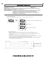
In the sequence program after replacement, two programs are required as shown below.
<Before transition>
<After transition>
Main routine
program
Main routine
program
END
Initial processing
FEND
P2
Subroutine
program
ASCII code is added to the input data area.
RET
END
1) Main routing program
y Set ‘0’ in the input data area on the rising edge of the execution instruction (‘M0’ in the program below) and
initialize the program.
y Execute the CALL instruction on every rising edge of the strobe signal (‘X108’ in the program below) so that
a subroutine program is called.
y In the subroutine program, input codes are added to the input data area and the completion status is checked.
y Pass the following data to the subroutine program at the execution of the CALL instruction.
y ASCII code input value from the input module (Xn0 to Xn7)
y Number of digits to be input.
y Indirect address of the input data area (Use the ADRSET instruction to acquire the indirect address for the
input data area.)
y Bit devices to be turned on when input is completed.
The input data area is initialized.
A subroutine program is called at
the rising edge of the strobe signal.
HEAD OFFICE : TOKYO BUILDING, 2-7-3 MARUNOUCHI, CHIYODA-KU, TOKYO 100-8310, JAPAN
NAGOYA WORKS : 1-14, YADA-MINAMI 5-CHOME, HIGASHI-KU, NAGOYA, JAPAN
TECHNICAL BULLETIN
[Issue No.] FA-A-0001-F
[Page] 28/58
[Title] Method of replacing High Performance model QCPU with Universal model QCPU
[Date of Issue] January 2008 (Ver. F: July 2011)
[Relevant Models] Q02UCPU, Q03UDCPU, Q04UDHCPU, Q06UDHCPU, Q10UDHCPU,
Q13UDHCPU, Q20UDHCPU, Q26UDHCPU, Q03UDECPU,
Q04UDEHCPU, Q06UDEHCPU, Q10UDEHCPU, Q13UDEHCPU,
Q20UDEHCPU, Q26UDEHCPU
2) Subroutine program
y In the subroutine program, ASCII codes specified by an argument are added to the input data area and the
completion status is checked.
y Specify the following arguments for the subroutine program.
First argument
Second argument
Third argument
Fourth argument
ASCII code input from the input module (K2Xn)
Number of digits to be input
Indirect address of the input data area
Bit device turned on when input is completed
(Input)
(Input)
(Input)
(Output)
Numeric entry is ended when
the at-completion ON signal is
ON or 0DH is input.
Addresses of the input data
area are saved in the work
devices.
The 1st to 4th digit numerals in
(input data area +2) areshifted
for one digit to the left.
Numeral entered in ASCII code
is converted into one numeral in
BIN data using the HABIN
instruction.
The 5th to 8th digit numerals in
(input data area +1) are
shifted for one digit to the left
and the converted numeral is
set to the 8th digit.
The number of digits to be input in
(input data area +0) is
incremented by one.
The at-completion ON signal is
turned ON when the input
processing for specified digits is
completed.
P3
HEAD OFFICE : TOKYO BUILDING, 2-7-3 MARUNOUCHI, CHIYODA-KU, TOKYO 100-8310, JAPAN
NAGOYA WORKS : 1-14, YADA-MINAMI 5-CHOME, HIGASHI-KU, NAGOYA, JAPAN
TECHNICAL BULLETIN
[Issue No.] FA-A-0001-F
[Page] 29/58
[Title] Method of replacing High Performance model QCPU with Universal model QCPU
[Date of Issue] January 2008 (Ver. F: July 2011)
[Relevant Models] Q02UCPU, Q03UDCPU, Q04UDHCPU, Q06UDHCPU, Q10UDHCPU,
Q13UDHCPU, Q20UDHCPU, Q26UDHCPU, Q03UDECPU,
Q04UDEHCPU, Q06UDEHCPU, Q10UDEHCPU, Q13UDEHCPU,
Q20UDEHCPU, Q26UDEHCPU
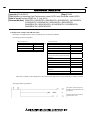
4. FUNCTIONS
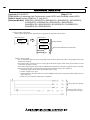
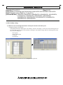
4.1 Floating-point Operation Instructions
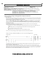
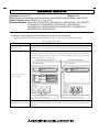
(1) Differences between the High Performance model QCPU and Universal model QCPU
(a) High Performance model QCPU
The High Performance model QCPU can perform only the single-precision floating-point operation instructions.
Note, however, that internal operation processing can be performed in double precision by selecting the item shown
below (default: selected).
Figure 4.1 PLC system tab
(b) Universal model QCPU
The Universal model QCPU supports the double-precision floating-point operation instructions.
The operation can be performed either in single precision or double precision depending on the data. Therefore,
“Perform internal arithmetic operations in double precision” item in the PLC system tab of the PLC parameter dialog
box cannot be selected.
Because of this new function, operation results (both in single precision and double precision) slightly differ between
the High Performance model QCPU and the Universal model QCPU if “Perform internal arithmetic operations in
double precision” is selected in the High Performance model QCPU.
If higher accuracy is required in floating-point operations, replace the floating-point operation instructions as described
in (4). However, if six or less digits are used as significant digits for the floating-point operation instructions,
replacement is not necessary. The single-precision floating-point operation results in the Universal model QCPU can
be used as they are in the system. When not replacing instructions, make sure that it does not cause any problems in the
system.
HEAD OFFICE : TOKYO BUILDING, 2-7-3 MARUNOUCHI, CHIYODA-KU, TOKYO 100-8310, JAPAN
NAGOYA WORKS : 1-14, YADA-MINAMI 5-CHOME, HIGASHI-KU, NAGOYA, JAPAN
TECHNICAL BULLETIN
[Issue No.] FA-A-0001-F
[Page] 30/58
[Title] Method of replacing High Performance model QCPU with Universal model QCPU
[Date of Issue] January 2008 (Ver. F: July 2011)
[Relevant Models] Q02UCPU, Q03UDCPU, Q04UDHCPU, Q06UDHCPU, Q10UDHCPU,
Q13UDHCPU, Q20UDHCPU, Q26UDHCPU, Q03UDECPU,
Q04UDEHCPU, Q06UDEHCPU, Q10UDEHCPU, Q13UDEHCPU,
Q20UDEHCPU, Q26UDEHCPU
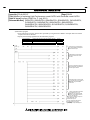
(2) Floating-point operation instructions for the Universal model QCPU
Table 4.1 lists floating-point operation instructions for the Universal model QCPU.
Specifications of the single-precision floating-point operation instructions are compatible with those for the High
Performance model QCPU.
Table 4.1 List of floating-point operation instructions supported in the Universal model QCPU
Instruction name
Instruction symbol
Single-precision floating-point data Double-precision floating-point data
LDE
Floating-point data comparison ANDE
ORE
Data transfer
Floating-point data transfer
EMOV(P)
Floating-point data addition
E+(P)
Floating-point data subtraction E-(P)
Four arithmetic
Floating-point data
operation
E*(P)
multiplication
Floating-point data division
E/(P)
Conversion from BIN 16-bit
FLT(P)
data to floating-point data
Conversion from BIN 32-bit
DFLT(P)
data to floating-point data
Data
Conversion from floating-point
conversion
INT(P)
data to BIN 16-bit data
Conversion from floating-point
DINT(P)
data to BIN 32-bit data
Floating-point sign inversion
ENEG(P)
SIN operation
SIN(P)
COS operation
COS(P)
TAN operation
TAN(P)
SIN-1 operation
ASIN(P)
COS-1 operation
ACOS(P)
Special
TAN-1operation
ATAN(P)
function
Conversion from angle to radian RAD(P)
Conversion from radian to angle DEG(P)
Square root
SQR(P)
Exponential operation
EXP(P)
Natural logarithm operation
LOG(P)
Comparison
LDED
ANDED
ORED
EDMOV(P)
ED+(P)
ED-(P)
Remarks
indicates one of the
followings;
<>, =, <, >, <=, >=
-
-
ED*(P)
ED/(P)
FLTD(P)
DFLTD(P)
-
INTD(P)
DINTD(P)
EDNEG(P)
SIND(P)
COSD(P)
TAND(P)
ASIND(P)
ACOSD(P)
ATAND(P)
RADD(P)
DEGD(P)
SQRD(P)
EXPD(P)
LOGD(P)
-
Floating-point data can be converted mutually between single precision and double precision using instructions in Table
4.2.
Table 4.2 Floating-point data conversion instructions (single precision
Instruction name
double precision)
Instruction symbol
Single precision to double precision conversion ECON(P)
Double precision to single precision conversion EDCON(P)
HEAD OFFICE : TOKYO BUILDING, 2-7-3 MARUNOUCHI, CHIYODA-KU, TOKYO 100-8310, JAPAN
NAGOYA WORKS : 1-14, YADA-MINAMI 5-CHOME, HIGASHI-KU, NAGOYA, JAPAN
TECHNICAL BULLETIN
[Issue No.] FA-A-0001-F
[Page] 31/58
[Title] Method of replacing High Performance model QCPU with Universal model QCPU
[Date of Issue] January 2008 (Ver. F: July 2011)
[Relevant Models] Q02UCPU, Q03UDCPU, Q04UDHCPU, Q06UDHCPU, Q10UDHCPU,
Q13UDHCPU, Q20UDHCPU, Q26UDHCPU, Q03UDECPU,
Q04UDEHCPU, Q06UDEHCPU, Q10UDEHCPU, Q13UDEHCPU,
Q20UDEHCPU, Q26UDEHCPU
(3) Advantages and disadvantages when using the double-precision floating-point data of the Universal model QCPU
Table 4.3 shows the advantages and disadvantages when executing the double-precision floating-point operation
instructions in the Universal model QCPU.
If higher accuracy is required in floating-point operations, it is recommended to replace the instructions with the
double-precision floating-point operation instructions.
Table 4.3 Advantages and disadvantages when using the double-precision floating-point operation instructions
Advantage
Disadvantage
The results are more accurate than those of the
The instruction processing speed is slower than that of the single-precision floating-point
single-precision floating-point operation instructions. operation instructions. *1
Double-precision floating-operation data use twice as many word device points as
single-precision floating-operation data.
*1: The processing speed of the double-precision floating-point operation instructions in the Universal model QCPU is higher than that
of floating-point operation instructions using internal double-precision operations in the High Performance model QCPU.
Table 4.4 shows the comparison between single-precision and double-precision floating-point data.
Table 4.4 Comparison between single-precision and double-precision floating-point data
Item
Word point required for data retention
Setting range
Mantissa part
Precision (number of bits)
Exponent part
Sign part
Data comparison
(Conductive status)
(LDE>= / LDED>=)
Instruction processing speed
Data transfer
(Q04UDHCPU/Q06UDHCPU) (EMOV/EDMOV)
(Maximum)
Addition (3 devices)
(E+ / ED+)
SIN operation
(SIN/SIND)
Single-precision floating-point data
Double-precision floating-point data
2 words
-2128<N -2-126,0,2-126 N<2128
23 bits
8 bits
1 bit
4 words
-21024<N -2-1022,0,2-1022 N<21024
52 bits
11 bits
1 bit
5.5μs
9.0μs
0.019μs
5.0μs
0.0665μs
9.2μs
5.7μs
13.8μs
HEAD OFFICE : TOKYO BUILDING, 2-7-3 MARUNOUCHI, CHIYODA-KU, TOKYO 100-8310, JAPAN
NAGOYA WORKS : 1-14, YADA-MINAMI 5-CHOME, HIGASHI-KU, NAGOYA, JAPAN
TECHNICAL BULLETIN
[Issue No.] FA-A-0001-F
[Page] 32/58
[Title] Method of replacing High Performance model QCPU with Universal model QCPU
[Date of Issue] January 2008 (Ver. F: July 2011)
[Relevant Models] Q02UCPU, Q03UDCPU, Q04UDHCPU, Q06UDHCPU, Q10UDHCPU,
Q13UDHCPU, Q20UDHCPU, Q26UDHCPU, Q03UDECPU,
Q04UDEHCPU, Q06UDEHCPU, Q10UDEHCPU, Q13UDEHCPU,
Q20UDEHCPU, Q26UDEHCPU
(4) Method of replacing the High Performance model QCPU with Universal model QCPU
(a) Replacing all single-precision floating-point operation instructions with double-precision floating-point operation
instructions
Single-precision floating-point data occupy two points of word device per data. On the other hand, four points are
required per double-precision floating-point data. Therefore, all device numbers for storing floating-point data need to
be reassigned.
Example) Replacing the floating-point operation ‘A×B+C’ (Changing all floating-point data into double precision.)
1) Device assignment
(Before replacement)
Application
(After replacement)
Device
Data A
D0 to D1
Data B
D2 to D3
Data C
D4 to D5
Operation result
D6 to D7
Data type
Floating-point data
(single precision)
Application
Device
Data A(D)
D0 to D3
Data B(D)
D4 to D7
Data C(D)
D8 to D11
Operation result(D)
D12 to D15
Data type
Floating-point data
(double precision)
2) Program before replacement
3) Program after replacement
Operation is performed using
double-precision floating-point
data.
HEAD OFFICE : TOKYO BUILDING, 2-7-3 MARUNOUCHI, CHIYODA-KU, TOKYO 100-8310, JAPAN
NAGOYA WORKS : 1-14, YADA-MINAMI 5-CHOME, HIGASHI-KU, NAGOYA, JAPAN
TECHNICAL BULLETIN
[Issue No.] FA-A-0001-F
[Page] 33/58
[Title] Method of replacing High Performance model QCPU with Universal model QCPU
[Date of Issue] January 2008 (Ver. F: July 2011)
[Relevant Models] Q02UCPU, Q03UDCPU, Q04UDHCPU, Q06UDHCPU, Q10UDHCPU,
Q13UDHCPU, Q20UDHCPU, Q26UDHCPU, Q03UDECPU,
Q04UDEHCPU, Q06UDEHCPU, Q10UDEHCPU, Q13UDEHCPU,
Q20UDEHCPU, Q26UDEHCPU
(b) Replacing a part of floating-point operation instructions with double-precision floating-point operation instructions
Only operations that require high accuracy are replaced with double-precision floating-point operation instructions.
Using the ECON and EDCON instructions, convert floating-point data mutually between single precision and double
precision. The flow of a replacement program is as follows:
y Data required for operations are converted from single precision to double precision using the ECON
instruction.
y Operations are performed in double precision using the double-precision floating-point operation instructions.
y Operation results are converted from double precision to single precision using the EDCON instruction.
A program example that floating-point data are converted mutually between single precision and double precision
before and after operations is shown below.
Example) Replacing the floating-point operation ‘A×B+C’ (Using the ECON and EDCON instructions)
1) Device assignment
(Before replacement)
Data A
Device
D0 to D1
Data B
D2 to D3
Data C
D4 to D5
Operation result
D6 to D7
Application
Data type
Floating-point data
(single precision)
(After replacement)
Application
Data A
Device
D0 to D1
Data B
D2 to D3
Data C
D4 to D5
Operation result
D6 to D7
Data A(D)
Data B(D)
Data C(D)
Operation result(D)
D10 to D13
D14 to D17
D18 to D21
D22 to D25
2) Program before replacement
HEAD OFFICE : TOKYO BUILDING, 2-7-3 MARUNOUCHI, CHIYODA-KU, TOKYO 100-8310, JAPAN
NAGOYA WORKS : 1-14, YADA-MINAMI 5-CHOME, HIGASHI-KU, NAGOYA, JAPAN
Data type
Floating-point data
(single precision)
Floating-point data
(double precision)
TECHNICAL BULLETIN
[Issue No.] FA-A-0001-F
[Page] 34/58
[Title] Method of replacing High Performance model QCPU with Universal model QCPU
[Date of Issue] January 2008 (Ver. F: July 2011)
[Relevant Models] Q02UCPU, Q03UDCPU, Q04UDHCPU, Q06UDHCPU, Q10UDHCPU,
Q13UDHCPU, Q20UDHCPU, Q26UDHCPU, Q03UDECPU,
Q04UDEHCPU, Q06UDEHCPU, Q10UDEHCPU, Q13UDEHCPU,
Q20UDEHCPU, Q26UDEHCPU
3) Program after replacement
Floating-point data are
converted from single precision
to double precision.
Operation is performed using
double-precision floating-point
data.
The floating-point operation result
data are converted from double
precision to singe precision.
(c) Replacing a part of floating-point operation instructions with double-precision floating-point operation instructions
using subroutine programs
The flow of a replacement program described in (b) can be regarded as one subroutine program. Create subroutine
programs for each floating-point operation instruction and then replace the original floating-point operation
instructions with the CALL(P) instructions so that the corresponding subroutine program is called.
With this method, changes in the program are minimized, but the processing for calling subroutine programs increases
the scan time. In addition, since conversions from double precision to single precision are performed for each
instruction, rounding-off errors generated during operations are larger than those in the replacement program described
in (b).
Example) Replacing the floating-point operation ‘A×B+C’ (Using a subroutine program)
1) Device assignment
(Before replacement)
Application
Device
Data A
D0 to D1
Data B
D2 to D3
Data C
D4 to D5
Operation result
D6 to D7
Data type
Floating-point data
(single precision)
(After replacement)
Application
Data A
Data B
Data C
Operation result
Device
D0 to D1
D2 to D3
D4 to D5
D6 to D7
Subroutine input data 1
D900 to D903
Subroutine input data 2
D904 to D907
Subroutine operation
result
D908 to D911
HEAD OFFICE : TOKYO BUILDING, 2-7-3 MARUNOUCHI, CHIYODA-KU, TOKYO 100-8310, JAPAN
NAGOYA WORKS : 1-14, YADA-MINAMI 5-CHOME, HIGASHI-KU, NAGOYA, JAPAN
Data type
Floating-point data
(single precision)
Floating-point data
(double precision)
TECHNICAL BULLETIN
[Issue No.] FA-A-0001-F
[Page] 35/58
[Title] Method of replacing High Performance model QCPU with Universal model QCPU
[Date of Issue] January 2008 (Ver. F: July 2011)
[Relevant Models] Q02UCPU, Q03UDCPU, Q04UDHCPU, Q06UDHCPU, Q10UDHCPU,
Q13UDHCPU, Q20UDHCPU, Q26UDHCPU, Q03UDECPU,
Q04UDEHCPU, Q06UDEHCPU, Q10UDEHCPU, Q13UDEHCPU,
Q20UDEHCPU, Q26UDEHCPU
2) Program before replacement
3) Program after replacement
A subroutine program for
multiplication using the
double-precision
floating-point operation
instruction
A subroutine program for
addition using the
double-precision
floating-point operation
instruction
HEAD OFFICE : TOKYO BUILDING, 2-7-3 MARUNOUCHI, CHIYODA-KU, TOKYO 100-8310, JAPAN
NAGOYA WORKS : 1-14, YADA-MINAMI 5-CHOME, HIGASHI-KU, NAGOYA, JAPAN
TECHNICAL BULLETIN
[Issue No.] FA-A-0001-F
[Page] 36/58
[Title] Method of replacing High Performance model QCPU with Universal model QCPU
[Date of Issue] January 2008 (Ver. F: July 2011)
[Relevant Models] Q02UCPU, Q03UDCPU, Q04UDHCPU, Q06UDHCPU, Q10UDHCPU,
Q13UDHCPU, Q20UDHCPU, Q26UDHCPU, Q03UDECPU,
Q04UDEHCPU, Q06UDEHCPU, Q10UDEHCPU, Q13UDEHCPU,
Q20UDEHCPU, Q26UDEHCPU
4.2 Error Check Processing for Floating-point Data Comparison Instructions
(1) Input data check
Error check processing for floating-point data comparison instructions has been enhanced for the Universal model QCPU.
Input of a "special value" (-0, nonnumeric, unnormalized number, or ±∞) is checked, and if any special value are input, the
CPU module detects “OPERATION ERROR” (error code: 4140).
When the LDE , ANDE , ORE , LDED , ANDED , and/or ORED instructions ( indicates one of the followings:
=, <>, <, >, <=, >=) are used in the program, “OPERATION ERROR” (error code: 4140) can be detected if invalid
floating-point data exist. This occurs even when interlocks are provided using the valid data flag (the signal which shows
the floating-point validity).
Invalid floating-point data are not stored as the result of operations performed in the Universal model QCPU.
Reasons for those invalid data are considered as follows:
y The same device is used for storing floating-point data and other data, such as binary values, BCD values, and
strings.
Use different devices for storing floating-point data and data other than floating-point data.
y Floating-point data externally written are invalid.
Take measures on the external-source side so that valid data are written.
If an error occurs in the floating-point data comparison instructions, take the above measures.
Example 1) Detecting “OPERATION ERROR” (error code: 4140) with the LDE instruction
[Ladder mode]
[List mode]
In the ladder block starting from step 104, the floating-point data comparison instructions of steps 105 and 109 are not
executed when M101 (valid data flag) is off.
However, the LDE<= instruction of step 105 and the ORE>= instruction of step 109 are executed regardless of the
execution result of the LD instruction of step 104 in the program above. Therefore, even when M101 is off, “OPERATION
ERROR (error code: 4140) will be detected in the LDE<= instruction of step 105 if a ‘special value’ is stored in D100.
For the method of avoiding “OPERATION ERROR”, refer to (2) in this section.
HEAD OFFICE : TOKYO BUILDING, 2-7-3 MARUNOUCHI, CHIYODA-KU, TOKYO 100-8310, JAPAN
NAGOYA WORKS : 1-14, YADA-MINAMI 5-CHOME, HIGASHI-KU, NAGOYA, JAPAN
TECHNICAL BULLETIN
[Issue No.] FA-A-0001-F
[Page] 37/58
[Title] Method of replacing High Performance model QCPU with Universal model QCPU
[Date of Issue] January 2008 (Ver. F: July 2011)
[Relevant Models] Q02UCPU, Q03UDCPU, Q04UDHCPU, Q06UDHCPU, Q10UDHCPU,
Q13UDHCPU, Q20UDHCPU, Q26UDHCPU, Q03UDECPU,
Q04UDEHCPU, Q06UDEHCPU, Q10UDEHCPU, Q13UDEHCPU,
Q20UDEHCPU, Q26UDEHCPU
Example 2) Not detecting “OPERATION ERROR” (error code: 4140) with the ANDE instruction
[Ladder mode]
[List mode]
In the ladder block starting from step 104, the ANDE<= instruction of step 105 is not executed when M101 (valid data
flag) is off.
The ANDE<= instruction of step 105 is not executed when M101 is off in the LD instruction of step 104 in the program
above. Therefore, when M101 is off, “OPERATION ERROR” (error code: 4140) will not be detected even if a ‘special
value’ is stored in D100.
Example 3) Detecting “OPERATION ERROR” (error code: 4140) in the ANDE instruction
[Ladder mode]
[List mode]
In the ladder block starting from step 104, the ANDE<= instruction of step 106 and the OR>= instruction of step 110 are
not executed when M101 (valid data flag) is off.
However, if M90 is on in the LD instruction of step 105, the ANDE<= instruction of step 106 is executed. Therefore, even
when M101 is off, “OPERATION ERROR” (error code: 4140) will be detected in the ANDE<= instruction of step 106 if
M90 is on and a ‘special value’ is stored in D100.
For the method of avoiding “OPERATION ERROR”, refer to (2) in this section.
HEAD OFFICE : TOKYO BUILDING, 2-7-3 MARUNOUCHI, CHIYODA-KU, TOKYO 100-8310, JAPAN
NAGOYA WORKS : 1-14, YADA-MINAMI 5-CHOME, HIGASHI-KU, NAGOYA, JAPAN
TECHNICAL BULLETIN
[Issue No.] FA-A-0001-F
[Page] 38/58
[Title] Method of replacing High Performance model QCPU with Universal model QCPU
[Date of Issue] January 2008 (Ver. F: July 2011)
[Relevant Models] Q02UCPU, Q03UDCPU, Q04UDHCPU, Q06UDHCPU, Q10UDHCPU,
Q13UDHCPU, Q20UDHCPU, Q26UDHCPU, Q03UDECPU,
Q04UDEHCPU, Q06UDEHCPU, Q10UDEHCPU, Q13UDEHCPU,
Q20UDEHCPU, Q26UDEHCPU
(2) Method of avoiding “OPERATION ERROR” (error code: 4140) in the floating-point data comparison
instructions
As shown in the modification examples below, connect a valid data flag contact to a floating-point data comparison
instruction is series. (Use the AND connection for connecting the contact of the valid data flag and floating-point data
comparison instruction.)
Make sure that there is no vertical line (the OR connection) between the valid data flag and floating-point data comparison
instruction.
<Modification example 1>
(Before modification)
(After modification)
E<=
D100
E10
E<=
D100
E10
E>=
D100
E200
Valid
data
flag
Valid
data
flag
D100
E>=
E200
Valid
data
flag
Make sure that there is no line (OR connection)
between the signal which shows the
floating-point data validity (valid data flag) and
the floating-point data comparison instruction.
<Modification example 2>
(Before modification)
E<=
(After modification)
D100
Valid
data
flag
E10
E<=
D100
M200
M201
Valid
data
flag
M200
M201
Valid
data
flag
HEAD OFFICE : TOKYO BUILDING, 2-7-3 MARUNOUCHI, CHIYODA-KU, TOKYO 100-8310, JAPAN
NAGOYA WORKS : 1-14, YADA-MINAMI 5-CHOME, HIGASHI-KU, NAGOYA, JAPAN
E10
TECHNICAL BULLETIN
[Issue No.] FA-A-0001-F
[Page] 39/58
[Title] Method of replacing High Performance model QCPU with Universal model QCPU
[Date of Issue] January 2008 (Ver. F: July 2011)
[Relevant Models] Q02UCPU, Q03UDCPU, Q04UDHCPU, Q06UDHCPU, Q10UDHCPU,
Q13UDHCPU, Q20UDHCPU, Q26UDHCPU, Q03UDECPU,
Q04UDEHCPU, Q06UDEHCPU, Q10UDEHCPU, Q13UDEHCPU,
Q20UDEHCPU, Q26UDEHCPU
Program examples corresponding to for Examples 1) and 3) in (1) are shown below.
Example 4) Modified program (Example 1) (“OPERATION ERROR” (error code: 4140) is no longer detected.)
[Ladder mode]
[List mode]
Example 5) Modified program (Example 3) (“OPERATION ERROR” (error code: 4140) is no longer detected.)
[Ladder mode]
[List mode]
HEAD OFFICE : TOKYO BUILDING, 2-7-3 MARUNOUCHI, CHIYODA-KU, TOKYO 100-8310, JAPAN
NAGOYA WORKS : 1-14, YADA-MINAMI 5-CHOME, HIGASHI-KU, NAGOYA, JAPAN
TECHNICAL BULLETIN
[Issue No.] FA-A-0001-F
[Page] 40/58
[Title] Method of replacing High Performance model QCPU with Universal model QCPU
[Date of Issue] January 2008 (Ver. F: July 2011)
[Relevant Models] Q02UCPU, Q03UDCPU, Q04UDHCPU, Q06UDHCPU, Q10UDHCPU,
Q13UDHCPU, Q20UDHCPU, Q26UDHCPU, Q03UDECPU,
Q04UDEHCPU, Q06UDEHCPU, Q10UDEHCPU, Q13UDEHCPU,
Q20UDEHCPU, Q26UDEHCPU
4.3 Range Check Processing for Index-modified Devices
(1) Device range check
Error check processing at index modification of devices has been enhanced for the Universal model QCPU.
Each index-modified device range is checked, and if the check target device is outside the device range before index
modification, the CPU module detects “OPERATION ERROR” (error code: 4101).
Example 1) Detecting “OPERATION ERROR” (error code: 4101) by error check processing at index modification of
devices
In Example 1), when the contact (M0) is on and the value, -1 or less, is specified in Z1, the device D0Z1 is included in the
C device range, exceeding the D device range, as shown in Figure 4.2.
As a result, “OPERATION ERROR” (error code: 4101) will be detected.
C0
When the value of Z1 is -1,
the device is included in the
C device range, resulting in an error.
C device area
D0
D device area
W0
W device area
Figure 4.2 Device D0Z1 when the value of Z1 is -1
When an error is detected, check the index modification value (value of Z1 in the above example) and remove the error
cause.
Examples of the cases where an error is detected and not detected are shown below.
HEAD OFFICE : TOKYO BUILDING, 2-7-3 MARUNOUCHI, CHIYODA-KU, TOKYO 100-8310, JAPAN
NAGOYA WORKS : 1-14, YADA-MINAMI 5-CHOME, HIGASHI-KU, NAGOYA, JAPAN
TECHNICAL BULLETIN
[Issue No.] FA-A-0001-F
[Page] 41/58
[Title] Method of replacing High Performance model QCPU with Universal model QCPU
[Date of Issue] January 2008 (Ver. F: July 2011)
[Relevant Models] Q02UCPU, Q03UDCPU, Q04UDHCPU, Q06UDHCPU, Q10UDHCPU,
Q13UDHCPU, Q20UDHCPU, Q26UDHCPU, Q03UDECPU,
Q04UDEHCPU, Q06UDEHCPU, Q10UDEHCPU, Q13UDEHCPU,
Q20UDEHCPU, Q26UDEHCPU
Example 2) Detecting “OPERATION ERROR” (error code: 4101)
[Ladder mode]
[List mode]
In Example 2, in the ladder block starting from the step 15, the AND < > instruction of the step 17 or 21 is supposed to be
not executed when M0 (valid data flag) is off.
However, since the LD instruction which is always executed is used in the step 16 and 20, the AND < > instruction of the
step 17 or 21 is executed regardless of the execution status of the LD instruction in the step 15 when M1 or M2 is on.
For this reason, even when M0 is off, if the D10Z1 value is outside the D device range, “OPERATION ERROR” (error
code: 4101) will be detected in the AND < > instruction of the step 17.
Note that the step 26 (MOV D0 D1) and the step 28 (INC D2) are not executed.
For the method of avoiding “OPERATION ERROR” (error code: 4101), refer to (2) in this section.
Example 3) Not detecting “OPERATION ERROR” (error code: 4101)
[Ladder mode]
[List mode]
In Example 3, the AND < > instruction of the step 16 is not executed when M0 (valid data flag) of the step 15 is off.
For this reason, “OPERATION ERROR” (error code: 4101) will not be detected no matter what the D10Z1 value is.
HEAD OFFICE : TOKYO BUILDING, 2-7-3 MARUNOUCHI, CHIYODA-KU, TOKYO 100-8310, JAPAN
NAGOYA WORKS : 1-14, YADA-MINAMI 5-CHOME, HIGASHI-KU, NAGOYA, JAPAN
TECHNICAL BULLETIN
[Issue No.] FA-A-0001-F
[Page] 42/58
[Title] Method of replacing High Performance model QCPU with Universal model QCPU
[Date of Issue] January 2008 (Ver. F: July 2011)
[Relevant Models] Q02UCPU, Q03UDCPU, Q04UDHCPU, Q06UDHCPU, Q10UDHCPU,
Q13UDHCPU, Q20UDHCPU, Q26UDHCPU, Q03UDECPU,
Q04UDEHCPU, Q06UDEHCPU, Q10UDEHCPU, Q13UDEHCPU,
Q20UDEHCPU, Q26UDEHCPU
(2) Method of avoiding “OPERATION ERROR” (error code: 4101)
When the index-modified device range does not need to be checked, use the method 1).
When the index-modified device range needs to be checked, use the method 2).
1) Deselect the “Check device range at indexing.” item in the PLC RAS tab of the PLC parameter dialog box so that the
index-modified device range will not be checked.
2) As shown in the modification examples below, connect the contacts of valid data flag in series for each instruction
that checks the index-modified device range.
<Modification example>
(Before modification)
(After modification)
[Ladder mode]
[Ladder mode]
M0
M0
M1
<>
Valid
data
flag
M1
<> D10Z1 K5
D10Z1 K5
Valid data
flag
M0
M2
M2
<> D10Z1 K10
<> D10Z1 K10
Valid data
flag
[List mode]
[List mode]
LD
LD
AND <>
LD
AND <>
ORB
ANB
M0
M1
D10Z1
M2
D10Z1
K5
K10
LD
AND
AND <>
LD
AND
AND <>
ORB
M0
M1
D10Z1
M0
M2
D10Z1
K5
K10
In the program before modification (on the left), the instruction immediately before the AND < > instruction is regarded as
the LD instruction. However, in the program after modification (on the right), the same instruction will be regarded as the
AND instruction.
In the program after modification, only when both contacts of M0 and M1 (or M2) turn on, the AND < > instruction is
executed. As a result, no error will be detected during index-modified device range check processing.
HEAD OFFICE : TOKYO BUILDING, 2-7-3 MARUNOUCHI, CHIYODA-KU, TOKYO 100-8310, JAPAN
NAGOYA WORKS : 1-14, YADA-MINAMI 5-CHOME, HIGASHI-KU, NAGOYA, JAPAN
TECHNICAL BULLETIN
[Issue No.] FA-A-0001-F
[Page] 43/58
[Title] Method of replacing High Performance model QCPU with Universal model QCPU
[Date of Issue] January 2008 (Ver. F: July 2011)
[Relevant Models] Q02UCPU, Q03UDCPU, Q04UDHCPU, Q06UDHCPU, Q10UDHCPU,
Q13UDHCPU, Q20UDHCPU, Q26UDHCPU, Q03UDECPU,
Q04UDEHCPU, Q06UDEHCPU, Q10UDEHCPU, Q13UDEHCPU,
Q20UDEHCPU, Q26UDEHCPU
4.4 Device Latch Function
(1) Overview
The device latch function*1 for the Universal model QCPU is more enhanced compared to that for the High performance
model QCPU.
This section describes the enhanced device latch function in the Universal model QCPU.
*1: The latch function is used to hold device data even when the CPU module is powered off or reset.
(2) Device data latch methods
Device data of the Universal model QCPU can be latched by:
y using a large-capacity file register (R, ZR),
y writing/reading device data to/from the standard ROM (with the SP.DEVST and S(P).DEVLD instructions), or
y specifying a latch range of internal user devices.
(3) Details of each latch method
(a) Large-capacity file registers (R, ZR)
File register size is larger and processing speed is higher in the Universal model QCPU, compared to the High
Performance model QCPU.
To latch a lot of data (many device points), use of a file register is effective.
Table 4.5 shows capacities of file registers for each CPU module.
Table 4.5 File register size available for each CPU module
File register (R, ZR) size in the standard RAM *1
Model
Q02UCPU
64K points
Q03UDCPU and Q03UDECPU
96K points
Q04UDHCPU and 04UDEHCPU
128K points
Q06UDHCPU and 06UDEHCPU
384K points
Q13UDHCPU and 13UDEHCPU
512K points
Q26UDHCPU and 26UDEHCPU
*1: Use of a memory card can increase the number of points.
640K points
(b) Writing/reading device data to/from the standard ROM (SP.DEVST/S(P).DEVLD instructions)
Device data of the Universal model QCPU can be latched using the SP.DEVST and S (P).DEVLD instructions
(instructions for writing/reading data to/from the standard ROM).
Utilizing the standard ROM allows data backup without batteries. This method is effective for latching data that will
be updated less frequently.
HEAD OFFICE : TOKYO BUILDING, 2-7-3 MARUNOUCHI, CHIYODA-KU, TOKYO 100-8310, JAPAN
NAGOYA WORKS : 1-14, YADA-MINAMI 5-CHOME, HIGASHI-KU, NAGOYA, JAPAN
TECHNICAL BULLETIN
[Issue No.] FA-A-0001-F
[Page] 44/58
[Title] Method of replacing High Performance model QCPU with Universal model QCPU
[Date of Issue] January 2008 (Ver. F: July 2011)
[Relevant Models] Q02UCPU, Q03UDCPU, Q04UDHCPU, Q06UDHCPU, Q10UDHCPU,
Q13UDHCPU, Q20UDHCPU, Q26UDHCPU, Q03UDECPU,
Q04UDEHCPU, Q06UDEHCPU, Q10UDEHCPU, Q13UDEHCPU,
Q20UDEHCPU, Q26UDEHCPU
(c) Specifying the latch range of internal user devices
Device data of the Universal model QCPU can be latched by specifying a latch range of internal user devices in the
same way as for the High Performance model QCPU.
The ranges can be set in the Device tab of the PLC parameter dialog box.
Internal user devices that can be latched are as follows:
y Latch relay (L)
y Link relay (B)
y Annunciator (F)
y Edge relay (V)
y Timer (T)
y Retentive timer (ST)
y Counter (C)
y Data register (D)
y Link register (W)
POINT
y If latch ranges of internal user devices are specified in the Universal model QCPU, the
processing time will increase in proportion to the points of the device to be latched. (For
example, if 8K points are latched for the latch relay (L), the scan time will be 28.6μs.) To
shorten the scan time, remove unnecessary latch device points to minimize the latch range.
y The scan time will not increase when a latch range of the file register (R, ZR) is specified.
(4) How to shorten the scan time
When data to be latched are stored in a file register (R or ZR), the processing time is shorter than that for latching internal
user device.
Example) Reducing the latch points of the data register (D) from 8K points to 2K points, and using the file register (ZR)
instead (when the Q06UDHCPU is used).
Table 4.6 Differences between before and after moving latch points of the data register (D) to the file register (ZR)
Item
Latch points for data register (D)
Number of devices in the program
Additional scan time
Data register (D) (Latch range)
File register (ZR) (Standard RAM)
Before
After
8192 (8K) points
2048 (2K) points
(6k points are moved to file register.)
400
100
0
300
0.41ms
0.13ms *1
Number of steps increased
*1: Indicates the time required additionally when file register data are stored in the standard RAM.
HEAD OFFICE : TOKYO BUILDING, 2-7-3 MARUNOUCHI, CHIYODA-KU, TOKYO 100-8310, JAPAN
NAGOYA WORKS : 1-14, YADA-MINAMI 5-CHOME, HIGASHI-KU, NAGOYA, JAPAN
300 steps
TECHNICAL BULLETIN
[Issue No.] FA-A-0001-F
[Page] 45/58
[Title] Method of replacing High Performance model QCPU with Universal model QCPU
[Date of Issue] January 2008 (Ver. F: July 2011)
[Relevant Models] Q02UCPU, Q03UDCPU, Q04UDHCPU, Q06UDHCPU, Q10UDHCPU,
Q13UDHCPU, Q20UDHCPU, Q26UDHCPU, Q03UDECPU,
Q04UDEHCPU, Q06UDEHCPU, Q10UDEHCPU, Q13UDEHCPU,
Q20UDEHCPU, Q26UDEHCPU
4.5 File Usability Setting
(1) Differences between the High Performance model QCPU and Universal model QCPU
(a) High Performance model QCPU
In the High Performance model QCPU, file usability ("Use PLC file setting" or "Not used") of the following files can
be set for each program on the screen opened by clicking the "File usability setting" button on the Program tab of the
PLC parameter dialog box.
y File register
y Device initial value
y Comment
y Local device
Figure 4.2 Program tab
HEAD OFFICE : TOKYO BUILDING, 2-7-3 MARUNOUCHI, CHIYODA-KU, TOKYO 100-8310, JAPAN
NAGOYA WORKS : 1-14, YADA-MINAMI 5-CHOME, HIGASHI-KU, NAGOYA, JAPAN
TECHNICAL BULLETIN
[Issue No.] FA-A-0001-F
[Page] 46/58
[Title] Method of replacing High Performance model QCPU with Universal model QCPU
[Date of Issue] January 2008 (Ver. F: July 2011)
[Relevant Models] Q02UCPU, Q03UDCPU, Q04UDHCPU, Q06UDHCPU, Q10UDHCPU,
Q13UDHCPU, Q20UDHCPU, Q26UDHCPU, Q03UDECPU,
Q04UDEHCPU, Q06UDEHCPU, Q10UDEHCPU, Q13UDEHCPU,
Q20UDEHCPU, Q26UDEHCPU
(b) Universal model QCPU
In the Universal model QCPU, file usability of the following files*1 cannot be set for each program on the screen
opened by clicking the "File usability setting" button on the Program tab of the PLC parameter dialog box.
y File register
y Device initial value
y Comment
Figure 4.3 File usability setting
*1: The local device file usability setting is also not available for the Universal model QCPU if the serial number (first five digits) is "10011" or earlier.
If the local device is set to be used in the PLC file tab of the PLC parameter dialog box in the High Performance model QCPU, all the programs use
the local device in the Universal model QCPU after replacement.
When the file usability setting is set in the High Performance model QCPU, change the setting in the following pages.
HEAD OFFICE : TOKYO BUILDING, 2-7-3 MARUNOUCHI, CHIYODA-KU, TOKYO 100-8310, JAPAN
NAGOYA WORKS : 1-14, YADA-MINAMI 5-CHOME, HIGASHI-KU, NAGOYA, JAPAN
TECHNICAL BULLETIN
[Issue No.] FA-A-0001-F
[Page] 47/58
[Title] Method of replacing High Performance model QCPU with Universal model QCPU
[Date of Issue] January 2008 (Ver. F: July 2011)
[Relevant Models] Q02UCPU, Q03UDCPU, Q04UDHCPU, Q06UDHCPU, Q10UDHCPU,
Q13UDHCPU, Q20UDHCPU, Q26UDHCPU, Q03UDECPU,
Q04UDEHCPU, Q06UDEHCPU, Q10UDEHCPU, Q13UDEHCPU,
Q20UDEHCPU, Q26UDEHCPU
(2) Method of replacing High Performance model QCPU with Universal model QCPU
Replacement method varies depending on the settings in the PLC file tab of the PLC parameter dialog box.
Table 4.7 Replacement method
Setting in the PLC file tab
“Not used.” is selected.
Setting in Universal model QCPU
No change in parameter setting is required.
Operation of the Universal model QCPU is the same regardless of the file usability setting in the High Performance
model QCPU.
When file usability is set to “Not used.” in the High Performance model QCPU, delete the corresponding program file
(file register, device initial value or comment), which uses the same name as the program, from the target memory.
The Universal model QCPU executes a program without using a program file if no program file that uses the same
name as the program exists in the target memory.
High Performance model QCPU
PLC parameter setting
PLC parameter setting
PLC file setting
PLC file setting
File register
setting
Universal model QCPU
Use the same file name as the
program.(Target memory: Memory
card (RAM))
File register
setting
Use the same file name as the
program.(Target memory: Memory
card (RAM))
Program setting
“Use the same file name as the
program.” is selected.
Program name File register
File
MAIN
Use PLC file setting
usability
Not used
SUB1
setting
Not used
SUB2
SRAM card
“Use the following file.” is selected.
SRAM card
MAIN
SUB1
SUB2
MAIN
File
register
File
register
File
register
File
register
SUB1
File
register
SUB2
File
register
Programs do not use file registers 'SUB1' and 'SUB2'
File registers 'SUB1' and 'SUB2' shall be deleted so that the
according to the "File usability setting".
programs 'SUB1' and 'SUB2' do not used them.
No change in parameter setting is required.
Operation of the Universal model QCPU is the same regardless of the file usability setting in the High Performance
model QCPU.
HEAD OFFICE : TOKYO BUILDING, 2-7-3 MARUNOUCHI, CHIYODA-KU, TOKYO 100-8310, JAPAN
NAGOYA WORKS : 1-14, YADA-MINAMI 5-CHOME, HIGASHI-KU, NAGOYA, JAPAN
TECHNICAL BULLETIN
[Issue No.] FA-A-0001-F
[Page] 48/58
[Title] Method of replacing High Performance model QCPU with Universal model QCPU
[Date of Issue] January 2008 (Ver. F: July 2011)
[Relevant Models] Q02UCPU, Q03UDCPU, Q04UDHCPU, Q06UDHCPU, Q10UDHCPU,
Q13UDHCPU, Q20UDHCPU, Q26UDHCPU, Q03UDECPU,
Q04UDEHCPU, Q06UDEHCPU, Q10UDEHCPU, Q13UDEHCPU,
Q20UDEHCPU, Q26UDEHCPU
4.6 Parameter-valid Drive and Boot File Setting
(1) Differences between the High Performance model QCPU and Universal model QCPU
(a) High Performance model QCPU
The parameter-valid drive is specified at the switches on the front panel of the High Performance model QCPU.
(b) Universal model QCPU
The Universal model QCPU automatically determines the parameter-valid drive, depending on the existence of
parameters in the drive (program memory, memory card or standard ROM). Therefore, when replacing the High
Performance model QCPU with the Universal model QCPU, changing the boot file setting for parameter and/or
moving files to another drive may be required.
When replacing the module, change the setting in the following pages.
HEAD OFFICE : TOKYO BUILDING, 2-7-3 MARUNOUCHI, CHIYODA-KU, TOKYO 100-8310, JAPAN
NAGOYA WORKS : 1-14, YADA-MINAMI 5-CHOME, HIGASHI-KU, NAGOYA, JAPAN
TECHNICAL BULLETIN
[Issue No.] FA-A-0001-F
[Page] 49/58
[Title] Method of replacing High Performance model QCPU with Universal model QCPU
[Date of Issue] January 2008 (Ver. F: July 2011)
[Relevant Models] Q02UCPU, Q03UDCPU, Q04UDHCPU, Q06UDHCPU, Q10UDHCPU,
Q13UDHCPU, Q20UDHCPU, Q26UDHCPU, Q03UDECPU,
Q04UDEHCPU, Q06UDEHCPU, Q10UDEHCPU, Q13UDEHCPU,
Q20UDEHCPU, Q26UDEHCPU
(2) Method of replacing the High Performance model QCPU with Universal model QCPU
(a) When the parameter-valid drive is set to the standard ROM in the High Performance model QCPU
Table 4.8 When the parameter-valid drive is set to the standard ROM
Setting in High Performance model QCPU
Setting in the Boot file tab of the PLC parameter dialog box
No boot file setting
Settings in the Boot file tab
Type
Transfer from
Program
Standard ROM
(No boot file setting for parameters)
Settings in the Boot file tab
Type
Transfer from
Program
Standard ROM
Parameter
Standard ROM
Settings in the Boot file tab
Type
Transfer from
Program
Memory card
(No boot file setting for parameters)
Settings in the Boot file tab
Type
Transfer from
Program
Memory card
Parameter
Memory card
Settings in the Boot file tab
Type
(Data other than
program and parameter)
Or
Type
(Data other than
program and parameter)
Transfer to
Program memory
Transfer to
Program memory
Program memory
Transfer to
Program memory
Transfer to
Program memory
Program memory
Transfer from
Memory card
Transfer to
Program
memory
Transfer from
Standard
ROM
Transfer to
Program
memory
Setting in Universal model QCPU
Change the setting so that the Universal model QCPU can refer to the parameters in the
standard ROM.
y Changes in parameter setting are not required.
y Delete parameters that exist in the program memory and memory card. *2
Change the setting so that programs are stored in the program memory in the first place,
instead of booting from the standard ROM.
y Delete all settings for parameter in the Boot file tab of the PLC parameter dialog box.
y Delete parameters that exist in the program memory and memory card. *2
y Move the programs with boot setting into the program memory from the standard
ROM. *1
Change the setting so that programs and parameters are stored in the program memory in the
first place, instead of booting from the standard ROM.
y Move the programs and parameters with boot setting into the program memory from the
standard ROM. *1
y Delete all settings for parameter in the Boot file tab of the PLC parameter dialog box.
Change the setting so that the Universal model QCPU can refer to the parameters in the
memory card and programs are booted from the memory card to the program memory.
y Move the parameters in the standard ROM into the memory card.
y Make setting so that programs are booted from the memory card to the program
memory in the Boot file tab of the PLC parameter dialog box. *3
Change the setting so that the Universal model QCPU can refer to the parameters in the
memory card and programs and parameters are booted from the memory card to the
program memory.
y Move the parameters in the standard ROM into the memory card.
y Make setting so that programs and parameters are booted from the memory card to the
program memory in the Boot file tab of the PLC parameter dialog box. *3
Delete all settings for data other than program and parameter in the boot file setting. Since
these data can be used even not stored in the program memory, it is not necessary to transfer
them to the program memory. Or, change the setting so that they are stored in the program
memory in the first place.
y Delete all settings for data other than program and parameter in the Boot file tab of the
PLC parameter dialog box.
y Move the data other than programs and parameters into the program memory as needed.
(Data other than program and parameter indicate initial device
value, device comment, and label program.)
*1: Since the Universal model QCPU holds the data in the program memory even when the battery voltage drops, the boot file setting is not necessary.
*2: The Universal model QCPU searches for parameters in order of in the program memory, in the memory card, and in the standard ROM. Then, the module
uses the parameters found first. If parameters exist in the program memory or the memory card, the Universal model QCPU cannot use the parameters in the
standard ROM.
*3: The Universal model QCPU ignores the boot file setting for parameters in the standard ROM.
HEAD OFFICE : TOKYO BUILDING, 2-7-3 MARUNOUCHI, CHIYODA-KU, TOKYO 100-8310, JAPAN
NAGOYA WORKS : 1-14, YADA-MINAMI 5-CHOME, HIGASHI-KU, NAGOYA, JAPAN
TECHNICAL BULLETIN
[Issue No.] FA-A-0001-F
[Page] 50/58
[Title] Method of replacing High Performance model QCPU with Universal model QCPU
[Date of Issue] January 2008 (Ver. F: July 2011)
[Relevant Models] Q02UCPU, Q03UDCPU, Q04UDHCPU, Q06UDHCPU, Q10UDHCPU,
Q13UDHCPU, Q20UDHCPU, Q26UDHCPU, Q03UDECPU,
Q04UDEHCPU, Q06UDEHCPU, Q10UDEHCPU, Q13UDEHCPU,
Q20UDEHCPU, Q26UDEHCPU
(b) When the parameter-valid drive is set to the memory card (RAM) or memory card (ROM) in the High Performance
model QCPU
Table 4.9 When the parameter-valid drive is set to the memory card (RAM) or memory card (ROM)
Setting in High Performance model QCPU
Setting in the Boot file tab of the PLC parameter dialog box
No boot file setting
Settings in the Boot file tab
Type
Transfer from
Program
Memory card
(No boot file setting for parameters)
Settings in the Boot file tab
Type
Transfer from
Program
Memory card
Parameter
Memory card
Settings in the Boot file tab
Type
Transfer from
Program
Standard ROM
(No boot file setting for parameters)
Settings in the Boot file tab
Type
Transfer from
Program
Standard ROM
Parameter
Memory card
Settings in the Boot file tab
Type
(Data other than
program and parameter)
Or
Type
(Data other than
program and parameter)
Transfer to
Program memory
Setting in Universal model QCPU
Change the setting so that the Universal model QCPU can refer to the parameters in the
memory card.
y Changes in parameter setting are not required.
y Delete parameters that exist in the program memory. *2
Change the setting so that the Universal model QCPU can refer to the parameters in the
memory card.
y Changes in parameter setting are not required.
y Delete parameters that exist in the program memory. *2
No changes are required.
Transfer to
Program memory
Program memory
Transfer to
Program memory
Transfer to
Program memory
Program memory
Transfer from
Memory card
Transfer to
Program
memory
Transfer from
Standard ROM
Transfer to
Program
memory
Change the setting so that programs are stored in the program memory in the first place,
instead of booting from the standard ROM.
y Move the programs targeted for booting from the standard ROM into the program
memory. *1
y Delete all settings for program in the Boot file tab of the PLC parameter dialog box.
y Delete parameters that exist in the program memory. *2
Change the setting so that programs are stored in the program memory in the first place,
instead of booting from the standard ROM.
y Move the programs targeted for booting from the standard ROM into the program
memory. *1
y Delete all settings for program in the Boot file tab of the PLC parameter dialog box.
Delete all settings for data other than program and parameter in the boot file setting. Since
these data can be used even not stored in the program memory, it is not necessary to transfer
them to the program memory. Or, change the setting so that they are stored in the program
memory in the first place.
y Delete all settings for data other than program and parameter in the Boot file tab of the
PLC parameter dialog box.
y Move the data other than program and parameter into the program memory as needed.
(Data other than program and parameter indicate initial device
value, device comment, and label program.)
*1: Since the Universal model QCPU holds the data in the program memory even when the battery voltage drops, the boot file setting is not necessary.
*2: The Universal model QCPU searches for parameters in order of in the program memory, in the memory card, and in the standard ROM. Then, the module
uses the parameters found first. If parameters exist in the program memory or the memory card, the Universal model QCPU cannot use the parameters in the
standard ROM.
HEAD OFFICE : TOKYO BUILDING, 2-7-3 MARUNOUCHI, CHIYODA-KU, TOKYO 100-8310, JAPAN
NAGOYA WORKS : 1-14, YADA-MINAMI 5-CHOME, HIGASHI-KU, NAGOYA, JAPAN
TECHNICAL BULLETIN
[Issue No.] FA-A-0001-F
[Page] 51/58
[Title] Method of replacing High Performance model QCPU with Universal model QCPU
[Date of Issue] January 2008 (Ver. F: July 2011)
[Relevant Models] Q02UCPU, Q03UDCPU, Q04UDHCPU, Q06UDHCPU, Q10UDHCPU,
Q13UDHCPU, Q20UDHCPU, Q26UDHCPU, Q03UDECPU,
Q04UDEHCPU, Q06UDEHCPU, Q10UDEHCPU, Q13UDEHCPU,
Q20UDEHCPU, Q26UDEHCPU
4.7 External Input/Output Forced On/Off Function
(1) Differences between the High Performance model QCPU and Universal model QCPU
(a) High Performance model QCPU
External input/output can be forcibly turned on/off on the screen opened by selecting [Online]→[Debug]→[Forced
input output registration/cancellation] in GX Developer.
(b) Universal model QCPU
If the serial number (first five digits) is "10041" or earlier, the external input/output forced on/off function cannot be
used.
External input/output can be forcibly turned on/off by using the replacement program described below.
(2) Method of replacing High Performance model QCPU with Universal model QCPU
As shown in Figure 4.4, add program names, “SETX” and “SETY”, in the Program tab of the PLC parameter dialog box.
<Before replacement>
<After replacement>
Figure 4.4 Modification in the Program tab of the PLC parameter setting
The following table shows the program setting of the “SETX” and “SETY”.
Table 4.10 Program setting of “SETX” and “SETY”
Program name
Execution type
Position where program is added
SETX
Scan
Start of Program setting (No.1)
SETY
Scan
End of Program setting
HEAD OFFICE : TOKYO BUILDING, 2-7-3 MARUNOUCHI, CHIYODA-KU, TOKYO 100-8310, JAPAN
NAGOYA WORKS : 1-14, YADA-MINAMI 5-CHOME, HIGASHI-KU, NAGOYA, JAPAN
TECHNICAL BULLETIN
[Issue No.] FA-A-0001-F
[Page] 52/58
[Title] Method of replacing High Performance model QCPU with Universal model QCPU
[Date of Issue] January 2008 (Ver. F: July 2011)
[Relevant Models] Q02UCPU, Q03UDCPU, Q04UDHCPU, Q06UDHCPU, Q10UDHCPU,
Q13UDHCPU, Q20UDHCPU, Q26UDHCPU, Q03UDECPU,
Q04UDEHCPU, Q06UDEHCPU, Q10UDEHCPU, Q13UDEHCPU,
Q20UDEHCPU, Q26UDEHCPU
Example) Forcibly turning X40, X77, and X7A on, and X41 and Y7B off
The programs, "SETX" and "SETY", turns on or off the X and Y devices, which have been registered for
forced on/off using the external input/output forced on/off function, at each scan using the SET and RST
instructions.
High Performance model QCPU
(1)
(2)
(3)
(4)
(5)
Universal model QCPU
y Program example of “SETX”
(1)
(2)
y Program example of “SETY”
(3)
(4)
(5)
HEAD OFFICE : TOKYO BUILDING, 2-7-3 MARUNOUCHI, CHIYODA-KU, TOKYO 100-8310, JAPAN
NAGOYA WORKS : 1-14, YADA-MINAMI 5-CHOME, HIGASHI-KU, NAGOYA, JAPAN
TECHNICAL BULLETIN
[Issue No.] FA-A-0001-F
[Page] 53/58
[Title] Method of replacing High Performance model QCPU with Universal model QCPU
[Date of Issue] January 2008 (Ver. F: July 2011)
[Relevant Models] Q02UCPU, Q03UDCPU, Q04UDHCPU, Q06UDHCPU, Q10UDHCPU,
Q13UDHCPU, Q20UDHCPU, Q26UDHCPU, Q03UDECPU,
Q04UDEHCPU, Q06UDEHCPU, Q10UDEHCPU, Q13UDEHCPU,
Q20UDEHCPU, Q26UDEHCPU
(3) Replacing the COM instruction
If the COM instruction is used, add subroutine calls for P10 and P11 before and after the COM instruction. (P10 and P11
are pointers shown in the program examples in (2).) When SM775 is on (Executes refresh set by SD778) and also the 0 bit
of SD778 is off (Do not execute I/O refresh), replacement of the instruction is not necessary.
(a) Program before replacement
Selection of refresh processing
during COM instruction execution
(b) Program after replacement
Selection of refresh processing
during COM instruction execution
HEAD OFFICE : TOKYO BUILDING, 2-7-3 MARUNOUCHI, CHIYODA-KU, TOKYO 100-8310, JAPAN
NAGOYA WORKS : 1-14, YADA-MINAMI 5-CHOME, HIGASHI-KU, NAGOYA, JAPAN
TECHNICAL BULLETIN
[Issue No.] FA-A-0001-F
[Page] 54/58
[Title] Method of replacing High Performance model QCPU with Universal model QCPU
[Date of Issue] January 2008 (Ver. F: July 2011)
[Relevant Models] Q02UCPU, Q03UDCPU, Q04UDHCPU, Q06UDHCPU, Q10UDHCPU,
Q13UDHCPU, Q20UDHCPU, Q26UDHCPU, Q03UDECPU,
Q04UDEHCPU, Q06UDEHCPU, Q10UDEHCPU, Q13UDEHCPU,
Q20UDEHCPU, Q26UDEHCPU
(4) Replacing the RFS instruction
If any I/O numbers targeted for forced on/off are included in the partial refresh range specified by the RFS instruction, add
subroutine calls for P10 and P11 before and after the RFS instruction. (P10 and P11 are pointers shown in the program
examples in (2).)
If no I/O number targeted for forced on/off is included, addition of subroutine calls for P10 and P11 is not necessary.
(a) When partial refresh for input (X) is executed by the RFS instruction
Add a subroutine call that executes forced input after the RFS instruction.
A subroutine call that executes
forced input is added.
(b) When partial refresh for output (Y) is executed by the RFS instruction
Add a subroutine call that executes forced output before the RFS instruction.
A subroutine call that executes
forced output is added.
(5) Restrictions
Replacements described in (2) to (4) do not apply in the following cases:
y Input and output targeted for forced on/off are referred to or changed using the direct input device (DX)/direct
output device (DY).
y Input and output targeted for forced on/off are referred to or changed within an interrupt program.
HEAD OFFICE : TOKYO BUILDING, 2-7-3 MARUNOUCHI, CHIYODA-KU, TOKYO 100-8310, JAPAN
NAGOYA WORKS : 1-14, YADA-MINAMI 5-CHOME, HIGASHI-KU, NAGOYA, JAPAN
TECHNICAL BULLETIN
[Issue No.] FA-A-0001-F
[Page] 55/58
[Title] Method of replacing High Performance model QCPU with Universal model QCPU
[Date of Issue] January 2008 (Ver. F: July 2011)
[Relevant Models] Q02UCPU, Q03UDCPU, Q04UDHCPU, Q06UDHCPU, Q10UDHCPU,
Q13UDHCPU, Q20UDHCPU, Q26UDHCPU, Q03UDECPU,
Q04UDEHCPU, Q06UDEHCPU, Q10UDEHCPU, Q13UDEHCPU,
Q20UDEHCPU, Q26UDEHCPU
5. SPECIAL RELAY AND SPECIAL REGISTER
The Universal model QCPU does not support the special relay and special register described in Section 5.1 and 5.2.
Replace them using the method described in the following table or delete the corresponding sections.
5.1 Special Relay List
Table 5.1 lists special relay not supported in the Universal model QCPU and measures.
Table 5.1 Special relay not supported in the Universal model QCPU and measures
Number
Name/Description
SM80
CHK detection
SM91
SM92
SM93
SM94
SM95
SM96
SM97
SM98
SM99
Step transition monitoring timer start
SM250
Largest mounted I/O number read
SM255
SM256
SM257
SM260
SM261
SM262
SM265
SM266
SM267
SM270
SM271
SM272
SM280
Indicates operative network or standby network
MELSECNET/H At refresh from link module to CPU, selects
whether to read data from the link module.
module 1
information
At refresh from CPU to link module, selects
whether to write data to the link module.
Measures
The Universal model QCPU does not support the CHK instruction.
For the replacing method of the CHK instruction, refer to Section 3.3.
The Universal model QCPU does not support the step transition
monitoring timer function.
For the alternative method of this function, refer to Appendix 3
"Restrictions on Basic Model QCPU, Universal Model QCPU, and
LCPU and Alternative Methods" in the MELSEC-Q/L/QnA
Programming Manual (SFC).
Operation of SD250 is not necessary. The Universal model QCPU always
stores the largest mounted I/O number in SD250. Delete the
corresponding parts.
These are special relays for the simple dual-structured network function.
Since the Universal model QCPU does not support this function, there is
no application for these special relays. Delete the corresponding sections.
Indicates operative network or standby network
MELSECNET/H At refresh from link module to CPU, selects
whether to read data from the link module.
module 2
information
At refresh from CPU to link module, selects
whether to write data to the link module.
Indicates operative network or standby network
MELSECNET/H At refresh from link module to CPU, selects
module 3
whether to read data from the link module.
information
At refresh from CPU to link module, selects
whether to write data to the link module.
Indicates operative network or standby network
MELSECNET/H At refresh from link module to CPU, selects
whether to read data from the link module.
module 4
information
At refresh from CPU to link module, selects
whether to write data to the link module.
CC-Link error
Replace the relay with the I/O signals (Xn0, Xn1, and XnF) of the
mounted CC-Link module.
(To the next page)
HEAD OFFICE : TOKYO BUILDING, 2-7-3 MARUNOUCHI, CHIYODA-KU, TOKYO 100-8310, JAPAN
NAGOYA WORKS : 1-14, YADA-MINAMI 5-CHOME, HIGASHI-KU, NAGOYA, JAPAN
TECHNICAL BULLETIN
[Issue No.] FA-A-0001-F
[Page] 56/58
[Title] Method of replacing High Performance model QCPU with Universal model QCPU
[Date of Issue] January 2008 (Ver. F: July 2011)
[Relevant Models] Q02UCPU, Q03UDCPU, Q04UDHCPU, Q06UDHCPU, Q10UDHCPU,
Q13UDHCPU, Q20UDHCPU, Q26UDHCPU, Q03UDECPU,
Q04UDEHCPU, Q06UDEHCPU, Q10UDEHCPU, Q13UDEHCPU,
Q20UDEHCPU, Q26UDEHCPU
Table 5.1 Special relay not supported on the Universal model QCPU and measures (continued)
Number
SM330
SM331
SM332
SM390
SM404
SM405
SM430
SM431
SM432
SM433
SM434
SM510
SM551
SM672
SM710
SM734
SM735
Name/Description
Measures
The Universal model QCPU does not support low-speed execution type
Operation mode for low-speed execution type program
programs.
Delete the corresponding parts.
Normal SFC program execution status
The Universal model QCPU supports only normal SFC programs. Delete
SM331 and SM332 which are used as interlocks or replace them with
Program execution management SFC program execution status
SM321.
Modify the program that the Module ready signal (Xn) is used as an
Access execution flag
interlock according to sample programs described in the manual for each
module.
ON for only 1 scan after RUN of low-speed execution type programs The Universal model QCPU does not support low-speed execution type
programs.
OFF for only 1 scan after RUN of low-speed execution type
Delete the corresponding parts or replace them with the special relays for
programs
scan execution type programs (SM402 and SM403).
User timing clock No.5 (for low-speed execution type programs)
The Universal model QCPU does not support low-speed execution type
programs.
User timing clock No.6 (for low-speed execution type programs)
Delete the corresponding parts or replace them with the special relays for
User timing clock No.7 (for low-speed execution type programs)
scan execution type programs (SM420 and SM424).
User timing clock No.8 (for low-speed execution type programs)
User timing clock No.9 (for low-speed execution type programs)
The Universal model QCPU does not support low-speed execution type
Low-speed execution type program executing flag
programs.
Delete the corresponding sections.
The Universal model QCPU does not support the service interval
Module service interval time read
measurement function.
Delete the corresponding sections.
When outside the range of the file register in the memory card is accessed,
the Universal model QCPU detects "OPERATION ERROR" (error code:
4101).
Memory card file register access range flag
Programming for detecting errors using this special realy is not necessary.
Delete the corresponding sections.
The Universal model QCPU does not support the CHK instruction.
CHK instruction priority flag
For the replacing method of the CHK instruction, refer to Section 3.3.
The Universal model QCPU executes the XCALL instruction on the rising
XCALL instruction execution condition specification
edge of execution condition as well. There is no application for this special
relay. Delete the corresponding sections.
The Universal model QCPU does not support the following instructions:
y SFC step comment readout instruction (S(P).SFCSCOMR)
SFC comment readout instruction in-execution flag
y SFC transition condition comment readout instruction
(S(P).SFCTCOMR)
Delete the corresponding sections.
Power supply OFF off detection flag
The Universal model QCPU does not store redundant power supply system
information in SM1780 to SM1783.
Power supply failure detection flag
Delete the corresponding sections.
Momentary power failure detection flag for power supply 1
(SM1780 to SM1783 are always off.)
Momentary power failure detection flag for power supply 2
SM1780 *1
SM1781 *1
SM1782 *1
SM1783 *1
*1: The special relay can be used if the serial number (first five digits) of the Universal model QCPU is "10042" or later.
HEAD OFFICE : TOKYO BUILDING, 2-7-3 MARUNOUCHI, CHIYODA-KU, TOKYO 100-8310, JAPAN
NAGOYA WORKS : 1-14, YADA-MINAMI 5-CHOME, HIGASHI-KU, NAGOYA, JAPAN
TECHNICAL BULLETIN
[Issue No.] FA-A-0001-F
[Page] 57/58
[Title] Method of replacing High Performance model QCPU with Universal model QCPU
[Date of Issue] January 2008 (Ver. F: July 2011)
[Relevant Models] Q02UCPU, Q03UDCPU, Q04UDHCPU, Q06UDHCPU, Q10UDHCPU,
Q13UDHCPU, Q20UDHCPU, Q26UDHCPU, Q03UDECPU,
Q04UDEHCPU, Q06UDEHCPU, Q10UDEHCPU, Q13UDEHCPU,
Q20UDEHCPU, Q26UDEHCPU
5.2 Special Register List
Table 5.2 lists special register not supported in the Universal model QCPU and measures.
Table 5.2 Special registers not supported in the Universal model QCPU and measures
Number
SD80
SD90
SD91
SD92
SD93
SD94
SD95
SD96
SD97
SD98
SD99
SD280
SD281
SD315
SD430
SD510
SD528
SD529
SD532
SD533
SD534
SD535
SD544
SD545
SD546
SD547
SD550
SD551
SD552
Name/Description
CHK number
Measures
The Universal model QCPU does not support the CHK instruction.
For the replacing method of the CHK instruction, refer to Section 3.3.
The Universal model QCPU does not support the step transition monitoring timer function.
For the replacing method of this function, refer to Appendix 3 "Restrictions on Basic Model QCPU,
Universal Model QCPU, and LCPU and Alternative Methods" in the MELSEC-Q/L/QnA
Programming Manual (SFC).
Step transition monitoring timer setting
value
Replace these registers with the I/O signals (Xn0, Xn1, and XnF) of the mounted CC-Link module.
CC-Link error
Service processing setting is available for the Universal model QCPU on the PLC system setting tab
of the PLC parameter dialog box.
Select “Specify service process time.” for the service processing setting parameter and set the service
processing time. Other setting methods can be selected as well.
The Universal model QCPU does not support low-speed execution type programs.
Low-speed scan counter
Delete the corresponding section or replace it with the special register for scan execution type
programs (SD420).
The Universal model QCPU does not support low-speed execution type programs.
Low-speed execution type program
Delete the corresponding section or replace it with the special register for scan execution type
number
programs (SD500).
The Universal model QCPU does not support low-speed execution type programs.
Current scan time for low-speed execution
Delete the corresponding sections or replace them with the special registers for scan execution type
type programs
programs (SD520 and SD521).
Minimum scan time for low-speed
The Universal model QCPU does not support low-speed execution type programs.
execution type programs
Delete the corresponding sections or replace them with the special registers for scan execution type
programs (SD524 to SD527).
Maximum scan time for low-speed
execution type programs
Cumulative execution time for low-speed The Universal model QCPU does not support low-speed execution type programs.
execution type programs
Delete the corresponding sections.
Execution time for low-speed execution
The Universal model QCPU does not support low-speed execution type programs.
type programs
Delete the corresponding sections.
Service interval measurement module
The Universal model QCPU does not support the service interval measurement function.
Delete the corresponding sections.
Service interval time
Time reserved for communication
processing
Program No. specification for PLAODP
The Universal model QCPU does not support the PLAODP instruction.
instruction
Delete the corresponding section.
SD1780 *1 Power supply off detection status
The Universal model QCPU does not store redundant power supply system information in SD1780 to
SD1783.
SD1781 *1 Power supply failure detection status
Delete the corresponding sections.
*1 Momentary power failure detection
SD1782
(SD1780 to SD1783 are always off.)
counter for power supply 1
*1 Momentary power failure detection
SD1783
counter for power supply 1
*1: The special register can be used if the serial number (first five digits)of the Universal model QCPU is "10042" or later.
SD720
HEAD OFFICE : TOKYO BUILDING, 2-7-3 MARUNOUCHI, CHIYODA-KU, TOKYO 100-8310, JAPAN
NAGOYA WORKS : 1-14, YADA-MINAMI 5-CHOME, HIGASHI-KU, NAGOYA, JAPAN
TECHNICAL BULLETIN
[Issue No.] FA-A-0001-F
[Page] 58/58
[Title] Method of replacing High Performance model QCPU with Universal model QCPU
[Date of Issue] January 2008 (Ver. F: July 2011)
[Relevant Models] Q02UCPU, Q03UDCPU, Q04UDHCPU, Q06UDHCPU, Q10UDHCPU,
Q13UDHCPU, Q20UDHCPU, Q26UDHCPU, Q03UDECPU,
Q04UDEHCPU, Q06UDEHCPU, Q10UDEHCPU, Q13UDEHCPU,
Q20UDEHCPU, Q26UDEHCPU
REVISIONS
Version
Print Date
-
January 2008
A
March 2008
Revision
First edition
y The following modules have been added. Q13UDHCPU, Q26UDHCPU
y The following chapters and sections have been modified in accordance with the version upgrade of
the Universal model QCPU. Chapter 1 (2), Chapter 2, Section 4.4
y The following modules have been added. Q03UDECPU, Q04UDEHCPU, Q06UDEHCPU,
Q13UDEHCPU, Q26UDEHCPU
y The following chapters and sections have been modified in accordance with the version upgrade of
B
the Universal model QCPU. Chapter 1 (1), (6), Chapter 2, Section 4.3, 4.6, 5.1, 5.2
May 2008
y Software listed in Chapter 2 (3) “Software need to be upgraded for the compatibility
with the Universal model QCPU” have been reviewed and modified.
y “GX Converter” has been added to the list in Chapter 2 (4) “Software not supported in the Universal
model QCPU”.
y The following modules have been added. Q10UDHCPU, Q20UDHCPU, Q10UDEHCPU,
C
December 2008
Q20UDEHCPU.
y The following chapters and sections have been modified in accordance with the version upgrade of
the Universal model QCPU. Chapter 1 , Chapter 2, Chapter 3.
D
January 2009
E
September 2009
Section 4.3 has been added.
F
July 2011
Chapter 1 (4); Two precaution items have been added to the following table. External communication.
The descriptions of the reference manuals or the references have been changed in accordance with the
composition changes of the manuals.
HEAD OFFICE : TOKYO BUILDING, 2-7-3 MARUNOUCHI, CHIYODA-KU, TOKYO 100-8310, JAPAN
NAGOYA WORKS : 1-14, YADA-MINAMI 5-CHOME, HIGASHI-KU, NAGOYA, JAPAN