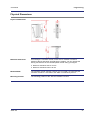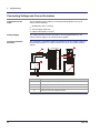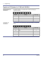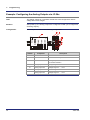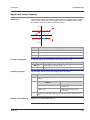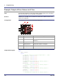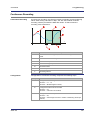
1
JX3-AO4 Analog Output Module 60873348 Introduction Item # 60873348 Revision 1.04.1 September 2012 / Printed in Germany Jetter AG reserve the right to make alterations to their products in the interest of technical progress. These alterations need not be documented in every single case. This User Manual and the information contained herein have been compiled with due diligence. However, Jetter AG assume no liability for printing or other errors or damages arising from such errors. The brand names and product names used in this document are trademarks or registered trademarks of the respective title owner. 2 Jetter AG JX3-AO4 Address Introduction How To Contact us: Jetter AG Graeterstrasse 2 D-71642 Ludwigsburg Germany Assignment to Product Phone - Switchboard: +49 7141 2550-0 Phone - Sales: +49 7141 2550-433 Phone - Technical Hotline: +49 7141 2550-444 Fax - Sales: +49 7141 2550-484 E-Mail - Sales: [email protected] E-Mail - Technical Hotline: [email protected] This User Manual is an integral part of JX3-AO4: Type: Serial #: Year of construction: Order #: To be entered by the customer: Inventory #: Place of operation: Jetter AG 3 Introduction Significance Significance of this User Manual The User Manual is an integral part of the device JX3-AO4: It must be kept in a way that it is always at hand, until the device JX3-AO4 will be disposed of. If the device JX3-AO4 is sold or loaned/leased out, the User Manual has to be passed on. In any case you encounter difficulties to clearly understand this User Manual, please contact the manufacturer. We would appreciate any suggestions and contributions on your part and would ask you to contact us by our e-mail address [email protected]. This will help us to produce manuals that are more user-friendly and to address your wishes and requirements. This User Manual contains important information on how to transport, erect, install, operate, maintain and repair the JX3-AO4. Therefore, the persons carrying out these jobs must carefully read, understand and observe this User Manual, and especially the safety instructions. Missing or inadequate knowledge of the User Manual results in the loss of any claim of liability on part of Jetter AG. Therefore, the operating company is recommended to have the instruction of the persons concerned confirmed in writing. 4 Jetter AG JX3-AO4 Contents Table of Contents 1 Safety Instructions 9 Generally Valid Safety Instructions .............................................................................................. 10 Instructions on EMI ...................................................................................................................... 12 2 Engineering 13 Product Description - JX3-AO4 .................................................................................................... 14 Parts and Interfaces of the JX3-AO4 Module .............................................................................. 15 Minimum Requirements ............................................................................................................... 16 JX3-Modules: List of Documentation ........................................................................................... 18 Accessories for the JX3 System .................................................................................................. 20 Physical Dimensions .................................................................................................................... 21 Assignment of Terminal X51 ........................................................................................................ 22 Assignment of Terminal X52 ........................................................................................................ 23 Specification of the Connectors for Terminals X51 / X52 ............................................................. 24 Internal Block Diagram ................................................................................................................. 25 Connecting Voltage and Current Actuators .................................................................................. 26 LEDs of the Module JX3-AO4 ...................................................................................................... 29 3 Installing, Replacing, and Removing the Module 30 Installing a JX3 Peripheral Module on a DIN Rail ........................................................................ 31 Replacing a JX3 Peripheral Module............................................................................................. 32 Removing a JX3 Peripheral Module from the DIN Rail................................................................ 34 4 First Commissioning 37 Preparing First Commissioning .................................................................................................... 38 First Commissioning by a JC-3xx ................................................................................................ 39 First Commissioning by a JC-24x ................................................................................................ 40 5 Programming 5.1 5.2 5.3 Jetter AG 41 Abbreviations, Module Register Properties and Formats ............................................................ 42 Register and I/O Numbering for JX3 Modules ........................................................................ 44 Registers and Module Registers .................................................................................................. 45 I/O Module Numbers in the JX2 System Bus .............................................................................. 46 Register and I/O Numbers with JC-24x and JM-D203-JC-24x .................................................... 47 Register and I/O Numbers with JC-3xx ....................................................................................... 48 Register and I/O Numbers for JC-647 with JX6-SB(-I) ................................................................ 49 Register and I/O Numbers for JC-800 with JX6-SB(-I) ................................................................ 50 Register and I/O Numbers for JC-9xx with JX6-SB(-I) ................................................................ 51 Register Access to JX3 Modules on the JX2 System Bus ..................................................... 52 Direct Register Access to JX3 Modules in the JX2 System Bus ................................................. 53 Example: Direct Register Access ................................................................................................. 54 Indirect Register Access to JX3 Modules on the JX2 System Bus .............................................. 55 Example: Indirect Register Access .............................................................................................. 57 Module Registers for Indirect Register Access ............................................................................ 58 Output of Voltages and Currents .............................................................................................. 59 Converting Digital Values into Analog Values .............................................................................. 60 5 Contents 5.4 5.4.1 5.4.2 5.4.3 5.4.4 5.5 6 Voltage Output ............................................................................................................................. 62 Current Output ............................................................................................................................. 64 Register Description: Voltage and Current Output ...................................................................... 66 Example: Configuring the Analog Outputs via JC-3xx ................................................................ 68 Example: Configuring the Analog Outputs via JC-24x ................................................................ 70 Additional Features ................................................................................................................... 72 User-Defined Scaling ................................................................................................................ 73 Function of User-Defined Scaling ............................................................................................... 74 Configuring User-Defined Scaling ............................................................................................... 76 Register Description: User-Defined Scaling ................................................................................ 78 Example: Scaling a Pressure Value via JC-3xx .......................................................................... 80 Example: Scaling a Pressure Value via JC-24x .......................................................................... 82 Limit Monitoring, Trailing Indicator, Cutting Off, and Forcing ............................................. 84 Monitoring Limit Values ............................................................................................................... 85 Trailing Indicator .......................................................................................................................... 87 Upper and Lower Capping .......................................................................................................... 89 Forcing the Analog Outputs ......................................................................................................... 91 Register Description .................................................................................................................... 93 Output of Error Values .............................................................................................................. 97 Configuring Error Values ............................................................................................................. 98 Register Description - Output of Error Values ........................................................................... 100 Example: Output of Error Values via JC-3xx ............................................................................. 102 Example: Output of Error Values via JC-24x ............................................................................. 104 Oscilloscope ............................................................................................................................ 106 Start/Stop Recording ................................................................................................................. 107 Continuous Recording ............................................................................................................... 109 Recording Values under Trigger Condition ................................................................................ 111 Reading Out the Recorded Values ............................................................................................. 114 Oscilloscope Register Description ............................................................................................. 115 Example: Recording and Reading of Values .............................................................................. 117 Status Monitoring via Collective Bits ..................................................................................... 119 Status Monitoring via Collective Bits ......................................................................................... 120 Register Description for Collective Bits ..................................................................................... 122 Locating of Errors 125 LEDs of the Module JX3-AO4 ................................................................................................... 126 Diagnostics of Error Messages via Module Registers .............................................................. 127 Error regarding Reference Values ............................................................................................. 129 Missing Connection to the Controller ........................................................................................ 130 Invalid Operating System .......................................................................................................... 131 DAC Error .................................................................................................................................. 132 Internal Auxiliary Voltages are Faulty ........................................................................................ 133 Register Description: Locating of Errors ................................................................................... 134 7 How to Identify the Module 137 Module Versions ........................................................................................................................ 138 Electronic Data Sheet (EDS) with JC-3xx ................................................................................. 140 Electronic Data Sheet (EDS) with JC-24x ................................................................................. 142 Electronic Data Sheet (EDS) with JC-647 and JX6-SB(-I)........................................................ 144 Example: Reading Out an EDS with JC-3xx ............................................................................. 146 Example: Reading Out an EDS with JC-24x ............................................................................. 148 Identification by Means of Module Registers ............................................................................ 150 Identification via Nameplate ...................................................................................................... 151 6 Jetter AG JX3-AO4 8 Contents Quick Reference - JX3-AO4 Appendix A: B: Jetter AG 153 155 Technical Data .......................................................................................................................... 156 Technical Data ............................................................................................................................ 157 Physical Dimensions .................................................................................................................. 158 Operating Parameters: Environment and Mechanics ................................................................ 159 Operating Parameters: Enclosure.............................................................................................. 160 DC Power Supply Inputs and Outputs ....................................................................................... 161 Shielded Data and I/O Lines ...................................................................................................... 162 Index .......................................................................................................................................... 163 7 JX3-AO4 1 Safety Instructions Safety Instructions Introduction This chapter informs the user of general safety instructions and warns of residual dangers, if applicable. Furthermore, it contains information on EMC. Contents Topic Page Generally Valid Safety Instructions ............................................................... 10 Instructions on EMI ....................................................................................... 12 Jetter AG 9 1 Safety Instructions Generally Valid Safety Instructions Introduction This device complies with the valid safety regulations and standards. Special emphasis was given to the safety of the users. Of course, the user should adhere to the following regulations: relevant accident prevention regulations; accepted safety rules; EC guidelines and other country-specific regulations Intended Conditions of Use Usage according to the intended conditions of use includes operation in accordance with this User Manual. The JX3-AO4 module is a JX3 peripheral module of four analog outputs for connection to analog actuators. It can be connected to the JX3 system bus. The JX3 system bus starts at the JX3-BN-xxx bus head or at the controller JC-3xx. By means of the bus head JX3-BN-CAN, the JX3-AO4 can be connected to the controllers JC-24x und JC-647, as well as to the dual axis controller JM-D203-JC24x. The JX3-AO4 module is supplied with voltage by the JC-3xx controllers or by the modules JX3-BN-XXX and JX3-PS1. This operating voltage is classified as SELV (Safety Extra Low Voltage). Therefore, the JX3-AO4 module is not subject to the EU Low Voltage Directive. The JX3-AO4 module may only be operated within the limits of the stated data, see chapter Technical Data (see page 157). The device is used to control machinery, such as conveyors, production machines, and handling machines. Usage Other than Intended This device must not be used in technical systems which to a high degree have to be fail-safe, e. g. ropeways and aeroplanes. If the device is to be run under ambient conditions which differ from the conditions mentioned in chapter Operating Conditions (see page 159), the manufacturer is to be contacted beforehand. Who may Operate the Device? Only instructed, trained and authorized persons are permitted to operate this device. Modifications and Alterations to the Device 10 Transport: Only by personnel with knowledge in handling electrostatically sensitive components. Installation: Only by specialists with training in electrical engineering. Engineering: Only by trained personnel, as specific know-how of electrical engineering is required. Commissioning: Only by specialists with profound knowledge of, and experience with, electrical engineering / drive technology. For safety reasons, no modifications and changes to the device and its functions are permitted. Any modifications to the device not expressly authorized by Jetter AG will result in a loss of any liability claims to Jetter AG. Jetter AG JX3-AO4 Safety Instructions The original parts are specifically designed for the device. Parts and equipment from other manufacturers are not tested on our part, and are, therefore, not released by Jetter AG. The installation of such parts may impair the safety and the proper functioning of the device. Any liability on the part of Jetter AG for any damages resulting from the use of non-original parts and equipment is excluded. Repair and Maintenance This device must not be repaired by the operators themselves. The device does not contain any parts that could be repaired by the operator. The device must be sent to Jetter AG for repair. Decommissioning and Disposal The environmental regulations of the respective country must be complied with when decommissioning and disposing of devices on the operating company's premises. Transporting JX3 Modules To exclude damages to JX3 modules the JX3 backplane bus has to be attached during transport. This is particularly true for transport via mail. Replacing Modules During exchange of JX3 modules, degree of protection IP20 is not ensured. Do not touch any electronic components once the JX3 module enclosure has been removed from the JX3 backplane module. Touching the EMC clip may result in damages to this clip and, thus, in lower noise immunity. Jetter AG 11 1 Safety Instructions Instructions on EMI Noise Immunity of a System The noise immunity of a system is determined by the weakest component of the system. For this reason, correct wiring and shielding of cables is of paramount importance. Measures to be Taken Measures for increasing immunity against EMI in electric plants: The JX3-AO4 module has to be attached to a DIN rail acc. to EN 50022-35 x 7.5. Follow the instructions given in Application Note 016 "EMC-Compatible Installation of the Electric Cabinet" published by Jetter AG. The following instructions are excerpts from Application Note 016: On principle, physical separation should be maintained between signal and power lines. We recommend spacings greater than 20 cm. Cables and lines should cross each other at an angle of 90°. The following line cables must be shielded: Analog lines, data lines, motor cables coming from inverter drives (servo output stage, frequency converter), lines between components and interference suppressor filter, if the suppressor filter has not been placed at the component directly. Shield cables at both ends. Unshielded wire ends of shielded cables should be as short as possible. The entire shield must, in its entire perimeter, be drawn behind the isolation, and then be clamped under an earthed strain relief with the greatest possible surface area. Download of Application Note 016 12 You can download Application Note 016 from our homepage http://www.jetter.de. The path leading to Application Note 016 "EMC-Compatible Installation of Electric Cabinets" is "Industrial Automation Support - Downloads - english - 7_Miscellaneous - Application Notes". Jetter AG JX3-AO4 2 Engineering Engineering Purpose of this Chapter This chapter is for supporting you when engineering a plant equipped with the JX3-AO4 module in the following fields of activity: Planning the wiring between the JX3-AO4 module and the analog actuator Selecting the analog actuators Connecting the analog actuators to the module JX3-AO4 Commissioning the JX3-AO4 module in the control cabinet Contents Topic Page Product Description - JX3-AO4 .................................................................... 14 Parts and Interfaces of the JX3-AO4 Module ............................................... 15 Minimum Requirements ................................................................................ 16 JX3-Modules: List of Documentation ............................................................ 18 Accessories for the JX3 System ................................................................... 20 Physical Dimensions .................................................................................... 21 Assignment of Terminal X51 ......................................................................... 22 Assignment of Terminal X52 ......................................................................... 23 Specification of the Connectors for Terminals X51 / X52 ............................. 24 Internal Block Diagram ................................................................................. 25 Connecting Voltage and Current Actuators .................................................. 26 LEDs of the Module JX3-AO4 ...................................................................... 29 Jetter AG 13 2 Engineering Product Description - JX3-AO4 The JX3-AO4 Module The JX3-AO4 module is a peripheral module for connection of analog actuators. This module is equipped with 4 analog outputs for voltages and currents. Characteristics The following list shows the characteristics of this module: Additional Features 14 4 analog outputs Resolution: 16 bits Selectable output signals per channel: 0 V ... +10 V, -10 V ... +10 V, 0 mA ... 20 mA, 4 mA ... 20 mA Accuracy: > 99.5 % Color of LED sheeting: sky-blue (RAL 5015) Additional features of the JX3-AO4 module are: Scope of Delivery User-scalable Monitoring and evaluation of limits Slave pointer Cutting off Forcing of analog outputs Error values Oscilloscope function Table function Operating system update by means of JetSym The following items are included in the scope of delivery of the JX3-AO4 module: Jetter item # Quantity Description 10000569 1 JX3-AO4 60869252 2 10-pin connector, spring cage technology 60870411 10 Terminal labels 60871899 1 Installation instruction 60870410 1 Keying pins Jetter AG JX3-AO4 Engineering Parts and Interfaces of the JX3-AO4 Module Parts and Interfaces The JX3-AO4 module features the following parts and interfaces: 6 Number Jetter AG Element Description 1 Upper latch 2 JX3 backplane module Connection of the JX3 modules, blue 3 X119 Connector for additional JX3 modules 4 JX3 module enclosure Can be dismounted from the JX3 backplane module, light grey coloring 5 Release lever For removing the JX3 module from the DIN rail 6 Lower latch For removing the JX3 module enclosure from the JX3 backplane module Not visible in the illustration 7 Terminal X52 Connection of analog outputs 3 and 4 8 Terminal X51 Connection of analog outputs 1 and 2 9 LEDs Diagnostics and status display For removing the JX3 module enclosure from the JX3 backplane module 15 2 Engineering Minimum Requirements Introduction The JX3-AO4 module is operated in a system consisting of various components supplied by Jetter AG. In order to ensure proper interaction of these components, the operating systems used and the programming tool JetSym must have the release numbers listed below. Configurations The module JX3-AO4 can be used in the following configurations: At a JetControl 3xx Connected to an Ethernet bus head JX3-BN-ETH Connected to the JX2 system bus of a JetControl 24x via CAN bus head JX3-BN-CAN Connected to the JX2 system bus of a dual axis controller JM-D203-JC24x via CAN bus head JX3-BN-CAN At a JX2 system bus of a JetControl 647 with a submodule JX6-SB(-I) via CAN bus head JX3-BN-CAN At a JX2 system bus of a JetControl 9xx with a submodule JX6-SB(-I) via CAN bus head JX3-BN-CAN Which is the earliest possible release of the operating system for the JX3-AO4 module is dependent on the hardware revision applied. You will find the hardware revision number on the nameplate fixed to the left cover of the enclosure. The release number of the operating system applied can be read out of MR 9. Hardware Revision Rev 01.xx.xx V 1.01.0.00 or higher Rev 03.xx.xx or higher V 1.03.0.00 or higher For the functions described in this document modules, controllers and software have to meet the following minimum requirements: BCDE A A ETHERNET F 01 2 BCDE LOW 2 9 10 1 2 3 4 11 12 3 4 5 6 13 14 5 6 7 8 15 16 7 8 0V 0V 24V RUN 0V 0V SHLD U2+ X19 U4+ I4+ POWER 0V 0V SHLD X10 DC24V 0,5A 0V 0V SHLD X52 I3+ 0V 0V SHLD SHLD SHLD U4+ I4+ X51 I2+ 5V ERR I3+ 0V E D1 D2 0V X52 0V R Jetter BUS OUT X15 I3+ JX3-AO4 E D1 D2 I1+ 0V U4+ X10 0V POWER BUS OUT ETHERNET SER SD-CARD X10 DC24V 1,2A 0V S33 1 R X18 OUTPUT INPUT INPUT MID 0V SHLD X52 X61 7 8 9 0V SER2 I2+ HIGH F 01 2 3 4 5 SHLD U2+ I2+ JetWeb JC-243 F 01 2 E 0V 0V SHLD Jetter ADRESS S31 3 4 56 POWER LOAD S32 0V U2+ 6 16 STOP RUN SER1 I1+ 0V X15 X11 Element E D1 D2 X51 X14 0V SHLD No. R Jetter I1+ X14 JX3-BN-CAN E D1 D2 BCD R X51 LOAD STOP 3 4 56 X19 A E D1 D2 Jetter S11 JX3-AO4 R JX3-BN-ETH JX3-AO4 E D1 D2 RUN 5 4 7 8 9 JC-340 R 3 BUS IN 2 1 7 8 9 Minimum Requirements Earliest Possible Operating System Release 6 Minimum Requirements of the Operating System 0V SHLD DC24V 0,5A 0V I4+ 0V 0V SHLD 6 Function 6 As of Release No. 1 JetSym Programming software V 3.00 2 JC-3xx PLC JetControl 3xx In preparation 3 JX3-BN-ETH Ethernet bus head In preparation 4 JC-24x PLC JetControl 240 V 3.23 Jetter AG JX3-AO4 Engineering No. Jetter AG Element Function As of Release No. JC-647 PLC JetControl 647 V 3.50 JX6-SB(-I) Submodule for system bus V 2.18 JM-D203-JC24x Dual axis controller with PLC JetControl 240 V 1.12.0.00 5 JX3-BN-CAN CAN bus head V 1.06.0.00 6 JX3-AO4 Analog output module V 1.03.0.00 17 2 Engineering JX3-Modules: List of Documentation Introduction Various documents and software tools will support the user when engineering and installing and programming the JX3-AO4 module. These documents and software tools can be downloaded from our homepage http://www.jetter.de. Engineering When performing engineering tasks, the following documents and files will support you: Data Sheet on the JX3-AO4 Module Product description Technical data Dimensional drawings User Manual on the JX3-AO4 Module The document at hand CAD Data of the JX3-AO4 Module 2D illustrations (dxf file) 3D illustrations (stp file) User Manual on the JC-3xx Control System Engineering at the JX2 System Bus Engineering a JX3 station Product descriptions of JX3 modules When engineering a JX3 station on the system bus (JC-24x and JC-647), the following document and software tool will support you: JX2-I/O System - User Information System bus topology Specification of the JX2 System Bus Product descriptions of JX3-BN-CAN, JX2 modules, IP67 modules and third-party modules System Bus Configurator 18 Excel file for designing the system bus SysBus_Configuration_xxx_e.xls (xxx: Version) Jetter AG JX3-AO4 Installation Engineering When installing such modules, the following document will support you: Installation Instruction It is included in the boxed module JX3-AO4 and contains the following information: Installation of the module on a DIN rail Terminal assignment Specification of conductor terminals Diagnostics via LEDs User Manual on the JX3-AO4 Module Programming The document at hand When programming the module, the following documents and software tools will support you: User Manual on the JX3-AO4 Module The document at hand JX2-I/O System - User Information Module numbering system Diagnostics of the modules on the JX2 system bus JetSym Programming tool User Manual of the Controller Jetter AG Depending on the controller used, you will need the corresponding manual 19 2 Engineering Accessories for the JX3 System Labelling Field Keying Pins Strain Relief for BU_10_E_BLZF_GE_RM 3.5 End Clamp for DIN Rail Screw Driver 20 Ten labelling fields are included in the scope of delivery of the JX3-AO4 module: Designation DIV_DEK_5/5_MC-10_NEUT._WS Jetter item # 60870411 VPE 100 pcs. One keying pin is included in the scope of delivery of the JX3-AO4 module: Designation DIV_BL_SL_3.5_KO_OR Jetter item # 60870410 Designation DIV_BL_3.5_ZE_8 Jetter item # 60870963 Designation DIV_CLIPFIX_35 Jetter item # 60863970 Type SD 0.4 x 2.5 - DIN 5264-A Designation DIV_SCHRAUBENDREHER_2.5*75 Jetter item # 60871712 Jetter AG JX3-AO4 Engineering Physical Dimensions Physical Dimensions Minimum Clearances At mounting the JX3-AO4 module, make sure to maintain a minimum clearance above and below. At replacing the module, you can operate the locking mechanisms of the JX3 backplane module using your fingers. Minimum clearance above: 30 mm Minimum clearance below: 25 mm Module Width The JX3-AO4 module requires a space of 31 mm width. At connecting the JX3-AO4 module to a JX3 station, the width is increased by 25 mm. Mounting Position The mounting position of the JX3-AO4 module is vertical. Jetter AG 21 2 Engineering Assignment of Terminal X51 Interfaces of Terminal X51 The signals of the following interfaces are connected to terminal X51: Analog output # 1 Analog output # 2 Assignment of Terminal X51 X51 I1+ 0V 0V SHLD U2+ I2+ 0V 0V SHLD Terminal Point U1+ Voltage output 1 I1+ Current output 1 0V Reference potential SHLD Shielding U2+ Voltage output 2 I2+ Current output 2 0V Reference potential SHLD 22 Function Shielding Jetter AG JX3-AO4 Engineering Assignment of Terminal X52 Interfaces of Terminal X52 The signals of the following interfaces are connected to terminal X52: Analog output # 3 Analog output # 4 Assignment of Terminal X52 X52 I3+ 0V 0V SHLD U4+ I4+ 0V 0V SHLD Terminal Point U3+ Voltage output 3 I3+ Current output 3 0V Reference potential SHLD Shielding U4+ Voltage output 4 I4+ Current output 4 0V Reference potential SHLD Jetter AG Function Shielding 23 2 Engineering Specification of the Connectors for Terminals X51 / X52 Ordering Data of the Connector Connector Specification Two 10-pin connectors already belong to the scope of delivery of the JX3-AO4 module: They can also be ordered individually by the following ordering data: Designation BU_10_BLZF_F_SW_RM3.5 Jetter item # 60869252 The connector is specified by the following list: Connector Specification Connector technology Spring cage connection Type 10-pin, contact spacing 3.5 mm Connectible Conductors Outer diameter of the isolation 2.90 mm max. AWG 16 ... 28 Terminal range 0.13 ... 1.5 mm Stripping length 10 mm 2 Specification Without Wire End Ferrules 2 One-wire H05(07) V-U 0.2 ... 1.5 mm Flexible H05(07) V-K 0.2 ... 1.5 mm 2 Specification With Wire End Ferrules Screw Driver 24 2 Bootlace ferrule without sleeve DIN 46228/1 0.2 ... 1.5 mm Bootlace ferrule with sleeve DIN 46228/4 0.2 ... 1.5 mm Crimping tool DIN 46228 PZ 4, PZ 6 ROTO, PZ 6/5 2 The fitting screw driver can be ordered from Jetter AG directly. Type SD 0.4 x 2.5 - DIN 5264-A Designation DIV_SCHRAUBENDREHER_2.5*75 Jetter item # 60871712 Jetter AG JX3-AO4 Engineering Internal Block Diagram Internal Block Diagram The JX3-AO4 module is equipped with four DAC for voltages and currents. FPGA µC X51.U1+ 10 nF D A X51.I1+ 10 nF X51.0V X51.U2+ 10 nF D A X51.I2+ 10 nF X52.U3+ A X52.I3+ 10 nF X52.U4+ A X52.I4+ 0Ω 10 nF Component Jetter AG U3/I3 X52.0V 10 nF D U2/I2 X51.0V 10 nF D U1/I1 U4/I4 X52.0V Function FPGA Communication component µC Controller D/A Digital-analog converter 10 nF Capacitor at the analog output 25 2 Engineering Connecting Voltage and Current Actuators Constituents of the Cable The constituents of the cable for connecting analog signals must, by all means, be the following: Shielded line, 85 % covering Tinned copper drain wire Cable cross section 0.14 mm2 The voltage actuator and the JX3 station can be supplied either by one common power supply or by various power supplies. Connecting Voltage Actuators The connection of voltage actuators is identical for all four analog outputs. In the following illustration, a voltage actuator has been connected to analog output 1. JX3-BN-CAN X51 R E D2 R E D2 Jetter X18 I1+ JX3-AO4 Voltage Supply X51 I1+ 0V BUS IN 0V 0V SHLD U2+ I2+ 0V 0V X19 0V SHLD BUS OUT X52 SHLD I3+ 0V 0V U2+ SHLD U4+ POWER X10 I4+ 0V 0V SHLD 0V 0V FE SHLD 0V 0V SHLD DC24V Signal I2+ DC24V 0,5A 0V DC24V 0V FE Number 26 Component 1 Cable leading to the analog actuator 2 Analog output module JX3-AO4 3 Voltage supply for JX3 station and analog actuator 4 Analog actuator with voltage-interface Jetter AG JX3-AO4 The connection of current actuators is identical for all four analog outputs. In the following illustration, a current actuator has been connected to analog output 1. JX3-BN-CAN X51 R E D2 R E D2 Jetter X18 I1+ JX3-AO4 Connecting Current Actuators Engineering X51 I1+ 0V BUS IN 0V 0V SHLD U2+ I2+ 0V 0V X19 0V SHLD BUS OUT X52 SHLD I3+ 0V 0V U2+ SHLD U4+ POWER X10 DC24V 0,5A 0V 0V 0V SHLD 0V 0V FE SHLD 0V 0V SHLD DC24V Signal I2+ I4+ DC24V 0V FE Number Improving the Noise Immunity Component 1 Cable leading to the analog actuator 2 Analog output module JX3-AO4 3 Voltage supply for JX3 station and analog actuator 4 Analog actuator with current interface For improving the noise immunity, please give heed to the following rules: Connect the copper drain wire (3) directly at the terminal point X51.SHLD, respectively X52.SHLD. Use a shielding terminal (2) for additionally earthing the shield of the wire. X52 I3+ 0V 0V SHLD U4+ I4+ 0V 0V SHLD Jetter AG 27 2 Engineering Number Component 1 Cable leading to the analog actuator 2 Shielding terminal 3 Tinned copper drain wire 4 Analog output module JX3-AO4 Related Topics Technical Data (see page 157) 28 Jetter AG JX3-AO4 Engineering LEDs of the Module JX3-AO4 The JX3-AO4 module signalizes states and errors via LEDs. This feature facilitates spotting an error immediately. R JX3-AO4 LEDs of the Module Normal Operating Condition LED Color R-LED green Run-LED E-LED red Error-LED D1-LED red Diagnose 1-LED D2-LED red Diagnose 2-LED ON E OFF D1 OFF D2 OFF Normal Operating Condition No error, communication is active The JX3-AO4 module is equipped with four LEDs to display states and errors. R E ON OFF ON ON ON ON ON Jetter AG Description The LEDs of the JX3-AO4 module have got the following states during normal operation: R LEDs of the JX3-AO4 Module E D1 D2 - D1 OFF - ON 2Hz D2 OFF State No error, communication is active - Communication with the bus head, respectively with the JC-3xx, is not active - Hardware error 1Hz 2Hz No valid operating system on the module Operating system update is active 29 3 Installing, Replacing, and Removing the Module 3 Installing, Replacing, and Removing the Module Introduction This chapter covers installation, replacement and removal of JX3 modules. Contents Topic Page Installing a JX3 Peripheral Module on a DIN Rail ......................................... 31 Replacing a JX3 Peripheral Module ............................................................. 32 Removing a JX3 Peripheral Module from the DIN Rail ................................ 34 30 Jetter AG JX3-AO4 Installing, Replacing, and Removing the Module Installing a JX3 Peripheral Module on a DIN Rail Installation To install a JX3 peripheral module on a rail to DIN EN 50022 proceed as follows: Step Action 1 Place the JX3 peripheral module on the upper edge of the DIN rail. 2 Snap the JX3 peripheral module onto the lower edge of the DIN rail. 3 Slide the JX3 peripheral module to the other modules of the JX3 station. Related Topics Replacing a JX3 Peripheral Module (see page 32) Removing a JX3 Peripheral Module from the DIN rail (see page 34) Jetter AG 31 3 Installing, Replacing, and Removing the Module Replacing a JX3 Peripheral Module Removing the JX3 Enclosure To remove the JX3 enclosure of the JX3 peripheral module from the JX3 backplane module proceed as follows: Step 1 Installing the JX3 Enclosure Action Remove power from the JX3 station. 2 Press the upper and lower latches. Keep the latches pressed. 3 Pull off the JX3 enclosure from the JX3 backplane module. To attach the enclosure of the JX3 peripheral module to the JX3 backplane module proceed as follows: Step 1 Action Slide the JX3 enclosure onto the JX3 backplane module until the latches snap into place. Result: Installation of the JX3 peripheral module to the JX3 backplane module is now completed. 32 Jetter AG JX3-AO4 Installing, Replacing, and Removing the Module Related Topics Installing JX3 Peripheral Modules on a DIN Rail (see page 31) Removing a JX3 Peripheral Module from the DIN Rail (see page 34) Jetter AG 33 3 Installing, Replacing, and Removing the Module Removing a JX3 Peripheral Module from the DIN Rail Removing To remove a JX3 peripheral module from a rail to DIN EN 50022 proceed as follows: Step 34 Action 1 Remove power from the JX3 station. 2 Slide the adjacent JX3 peripheral modules aside. By doing so, the JX3 backplane to the other JX3 peripheral modules is disconnected. 3 Pull down the DIN rail latch. 4 Swing the lower part of the JX3 peripheral module forward. Jetter AG JX3-AO4 Installing, Replacing, and Removing the Module Step 5 Action Remove the JX3 peripheral module from the DIN rail. Related Topics Installing JX3 Peripheral Modules on a DIN Rail (see page 31) Replacing a JX3 Peripheral Module (see page 32) Jetter AG 35 JX3-AO4 4 First Commissioning First Commissioning Purpose of this Chapter This chapter deals concisely with the first commissioning procedure of the JX3-AO4 module. The following function is to serve as an example: Voltage Output at Analog Output OUT 1 Prerequisites For first commissioning the JX3-AO4 module, the following requirements have to be met: The JX3-AO4 module is connected to a JetControl device. The controller is linked with a PC. On the PC, the JetSym programming software has been installed. The minimum requirements regarding module, controllers and software have been met. Contents Topic Page Preparing First Commissioning .................................................................... 38 First Commissioning by a JC-3xx ................................................................. 39 First Commissioning by a JC-24x ................................................................. 40 Jetter AG 37 4 First Commissioning Preparing First Commissioning Behavior After Power-Up In order to output a certain voltage, the JX3-AO4 module need not be configured after power-up. After power-up, the behavior of the four analog outputs is as follows: Configured to voltage range -10 V ... +10 V At the analog outputs, 0 V is output Any additional functions do not influence the output voltage For defect-free commissioning, the LEDs must have the following statuses: JX3-AO4 Status of the LEDs R E D1 D2 Component Terminal Points of Analog Output OUT 1 Status Description R-LED green, lit Logic supply of the module is ok E-LED off Communication active D1-LED off No error detected D2-LED off No error detected The module outputs the voltage at analog output OUT 1 at terminal points U1+ and 0 V of connector X 51: X51 U I1+ 0V 0V SHLD U2+ I2+ 0V 0V SHLD 38 Jetter AG JX3-AO4 First Commissioning First Commissioning by a JC-3xx D2 R E D1 D2 RUN 3 4 7 8 R D2 E 1 2 3 5 6 7 4 8 9 10 11 12 13 14 15 16 X21 X21 LOAD BUS OUT ETHERNET X14 X61 1 1 2 2 0V 3 3 SHLD 4 4 U2+ 5 5 I2+ 6 6 0V 7 SD-CARD DC24V 1,2A 0V Number 7 0V 8 SHLD 0V I3+ SER X10 I1+ 0V X52 X15 X11 POWER D2 2 6 X51 STOP Determining the Register Number E 1 5 13 14 15 16 X19 S11 R 9 10 11 12 Jetter JX3-DIO16 E JX3-AO4 R JX3-DI16 The first commissioning procedure is based on the following configuration: JC-360 Configuration 8 0V X22 X32 9 9 0V 10 10 0V 11 11 SHLD 12 12 U4+ 13 13 I4+ 14 14 0V 15 15 0V 16 16 SHLD 0V 0V Component Description 1 JC-3xx Controller 2 JX3-AO4 Analog output module, module number 2 3 JX3 Modules Further JX3 modules of the JX3 station 4 X51 Terminal for analog output OUT 1 The value of analog output OUT 1 has been assigned to module register MR 2. This register number consists of the following digits: 1 0 0 m m Element mm Voltage Output via JetSym 0 0 2 Meaning Module number of the module in the JX3 station: here 02 How to output a voltage at analog output OUT 1 via JetSym setup and register number 100020002: Number 1 Jetter AG 0 Description Values New value for analog output OUT 1 0 = 0 V 32767 = +10 V 39 4 First Commissioning First Commissioning by a JC-24x The first commissioning procedure is based on the following configuration: STOP LOAD Jetter ADDRESS S31 SER1 JetWeb JC-246 HIGH SER2 S32 MID S33 LOW E D1 D2 1 2 9 10 1 2 3 4 11 12 3 4 5 6 13 14 5 6 7 8 15 16 7 8 R E D1 D2 Jetter X18 OUTPUT INPUT INPUT R X51 I1+ 0V BUS IN RUN JX3-AO4 JX3-BN-CAN Configuration 0V SHLD U2+ I2+ 0V X19 ERR 0V SHLD 24V X52 RUN BUS OUT 5V I3+ 0V 0V SHLD U4+ X10 DC24V 0,5A 0V Number Determining the Register Number Component 0V SHLD Description JC-24x Controller 2 JX3-BN-CAN Bus head for JX2 system bus 3 JX3-AO4 Analog output module, I/O module number 2 4 X51 Terminal for analog output OUT 1 The value of analog output OUT 1 has been assigned to module register MR 2. This register number consists of the following digits: x x 2 Element xx Meaning I/O module number of the module on the system bus - 2 here: xx = 00 How to output a voltage at analog output OUT 1 via JetSym setup and register number 3002: Number 1 40 0V 1 3 Voltage Output via JetSym I4+ Description Values New value for analog output OUT 1 0 = 0 V 32767 = +10 V Jetter AG JX3-AO4 5 Programming Programming Objective of this Chapter This chapter supports programming the JX3-AO4 module in the following aspects: Determining register numbers dependent on the system configuration Output of voltages and currents Function and programming of additional functions Prerequisites For programming the JX3-AO4 module, the following requirements have to be met: The JX3-AO4 module is connected to a JetControl device. The controller is linked with a PC. On the PC, the JetSym programming software has been installed. The minimum requirements regarding module, controllers and software have been met. Contents Topic Page Abbreviations, Module Register Properties and Formats ............................. 42 Register and I/O Numbering for JX3 Modules .............................................. 44 Register Access to JX3 Modules on the JX2 System Bus ........................... 52 Output of Voltages and Currents .................................................................. 59 Additional Features ....................................................................................... 72 Status Monitoring via Collective Bits ............................................................ 119 Jetter AG 41 5 Programming Abbreviations, Module Register Properties and Formats Abbreviations In the following table, the abbreviations used in this document have been listed: Abbreviation Module Registers with y R 100 Register 100 MR 150 Module register 150 The letter y designates module registers, the function of which is identical for all four analog outputs. For y, enter the number of the analog output. 1 y z z No. Module Register Properties Meaning Element 1 y = 1 ... 4 Number of the analog output 2 zz = 0 ... 99 Continuous number Each module register is characterized by certain properties. For many module registers most properties are identical. For example, their value after reset is 0. In the following description, module register properties are mentioned only, if a property deviates from the following default properties. Module Register Properties Number Formats Meaning Default Property for Most Module Registers Access Read / write Value following a reset 0, or undefined (e.g. version number) Takes effect Immediately Write access Always Data type Integer In the following table, the number formats used in this document have been listed: Presentation 42 Number Format 100 Decimal 0x100 Hexadecimal 0b100 Binary Jetter AG JX3-AO4 JetSym Sample Programs Programming The notation for sample programs used in this document is listed in the following table: Notation Jetter AG Meaning Var, When, Task Key word BitClear(); Instructions 100 0x100 0b100 Constant numeric values // this is a comment Comment // ... Further program processing 43 5 Programming 5.1 Register and I/O Numbering for JX3 Modules Introduction The modules supplied by Jetter AG can carry out a great number of functions which can be called up by the user via registers. Each register and each digital input or output has been designated by an unambiguous number. Usage: Register Number Register numbers are used in the following cases: A module register is to be read or written in the Setup section of JetSym. A module register is to be declared as a variable in the application program Usage: I/O Number of JetSym. A module register is to be declared as a tag in JetViewSoft. I/O numbers are used in the following cases: A digital input is to be read in the Setup section of JetSym. A digital output is to be read or written in the Setup section of JetSym. A digital input or output is to be declared as a variable in the application program of JetSym. A digital input or output is to be declared as a tag in JetViewSoft. Contents Topic Page Registers and Module Registers ................................................................... 45 I/O Module Numbers in the JX2 System Bus ............................................... 46 Register and I/O Numbers with JC-24x and JM-D203-JC-24x ..................... 47 Register and I/O Numbers with JC-3xx ........................................................ 48 Register and I/O Numbers for JC-647 with JX6-SB(-I) ................................. 49 Register and I/O Numbers for JC-800 with JX6-SB(-I) ................................. 50 Register and I/O Numbers for JC-9xx with JX6-SB(-I) ................................. 51 44 Jetter AG JX3-AO4 Programming Registers and Module Registers Definition: Module Registers By means of module registers, process, configuration and diagnostic data can be read by the JX3-AO4 module, or written to the module. The module register number is unambiguous within the respective module. Definition: Registers Registers can be accessed directly in the application program of the controller, in a setup pane of JetSym, or via the user interface directly. The register number is unambiguous within the respective system. Example: Module Register Via module register 9, the up-to-date operating system version of a JX3-AI4 can be accessed. Example: Register A JX3-AI4 module has been connected to the system bus of a JC- 24x by a JX3-BN-CAN bus head. The module has got I/O module number 2. 1 3 0 2 No. 0 z 3 Element Meaning 1 Register number Can be used immediately 2 Register prefix 300: for JX3 modules at the system bus of a JC-24x 3 Module register number z = 9: OS version In the setup pane of JetSym, the operating system version 1.2.0.0 can be read out via register number 3009 directly. Counterexample: Module Register Jetter AG If in the setup pane of JetSym number 9 is entered, the operating system version is not read out. 45 5 Programming I/O Module Numbers in the JX2 System Bus I/O Module Number Each module in the JX2 system bus is assigned an I/O module number for clear identification. The I/O module number is dependent on the position of the module on the JX2 system bus. Assigning this module number is carried out according to the following rules: The controller has always got I/O module number 1. JX3-BN-CAN modules are counted separately. The first JX3-BN-CAN is assigned I/O module number 33. The JX2-PS1 and JX3-PS1 modules are not assigned an I/O module number. The first non-intelligent JX2, or JX3 module is assigned I/O module number INPUT BCD A MID 7 8 9 F 01 2 BCD A 3 4 56 E LOW 7 8 9 5V 24V ERR RUN INPUT OUTPUT 1 2 9 10 1 2 3 4 11 12 3 4 5 6 13 14 5 6 7 8 15 16 7 8 D2 X18 X21 1 2 BUS OUT 46 8 X21 R E D2 Jetter X18 1 2 R E D2 1 2 3 4 5 6 7 8 9 10 11 12 X21 1 5 R E D2 13 14 15 16 2 3 4 5 X21 1 2 3 4 5 6 6 6 6 7 7 7 7 8 0V 8 0V X19 X32 9 9 10 10 11 Module 4 7 3 12 Number 3 4 13 DC24V 0,5A 0V D2 2 6 9 10 11 12 3 X22 X10 E 1 5 4 5 X19 R 13 14 15 16 JX3-DIO16 E JX3-DI16 R JX3-BN-CAN D2 Jetter JX3-DIO16 E BUS IN HIGH F 01 2 E 34 56 S33 R 11 14 15 16 16 0V 0V 9 10 11 12 12 13 14 15 8 0V X22 BUS OUT BCD A S31 S32 JetWeb JC-246 F 01 2 E 34 56 SER1 SER2 Jetter ADDRESS 7 8 9 LOAD JX3-DI16 STOP RUN JX3-BN-CAN Several JX3 modules have been connected to a JC-24x controller via JX2 system bus. BUS IN Example: I/O Module Numbering 2. Intelligent JX2 modules, e.g. JX2-SV1, are not assigned an I/O module number. 13 X10 DC24V 0,5A 0V 8 0V X32 9 10 11 12 13 14 14 15 15 16 16 0V 0V I/O module number 1 JC-24x 1 2 JX3-BN-CAN 33 3 JX3-AO4 2 4 JX3-DIO16 3 5 JX3-BN-CAN 34 6 JX3-DI16 5 7 JX3-AI4 6 Jetter AG JX3-AO4 Programming Register and I/O Numbers with JC-24x and JM-D203-JC-24x The register number for JX3 modules with JC-24x and JM-D203-JC-24x is composed as follows: 3 x x z Element Meaning xx z 0 ... 30 At the bus head JX3-BN-CAN 31 ... 61 Module register number x x z z Element Meaning I/O module number in the JX2 system bus 2 ... 32 zz I/O number of the module 1 ... 16 STOP LOAD BCD A A BCD E INPUT MID 7 8 9 A BCD F 01 2 3 4 56 E HIGH F 01 2 3 4 56 S33 JetWeb JC-246 F 01 2 E 3 4 56 S32 SER2 Jetter ADDRESS S31 7 8 9 RUN LOW INPUT OUTPUT 1 2 9 10 1 2 3 4 11 12 3 4 5 6 13 14 5 6 7 8 15 16 7 8 R E D2 Jetter X18 R E 1 2 3 4 5 6 7 8 D2 9 10 11 12 13 14 15 16 X21 1 7 8 9 ERR X19 BUS OUT Number Module 7 D2 4 8 X21 1 2 4 0V 9 X10 3 6 3 8 X22 DC24V 0,5A 0V 2 9 10 11 12 4 5 RUN E 1 5 2 7 24V R 13 14 15 16 3 6 5V JX3-DIO16 Several JX3 modules have been connected to a JC-24x controller. SER1 Jetter AG Value range xx JX3-DI16 Example 0 ... 9 The I/O number for JX3 modules with JC-24x and JM-D203-JC-24x is composed as follows: JX3-BN-CAN I/O Numbers for JX3 Modules Value range I/O module number in the JX2 system bus - 2 BUS IN Register Numbers for JX3 Modules 5 6 7 8 0V X32 9 10 10 11 11 12 12 13 13 14 14 15 15 16 16 0V 0V I/O module number Register I/O 1 JC-24x 1 0 ... 1999 101 ... 116 2 JX3-BN-CAN 33 3310 ... 3319 - 3 JX3-DI16 2 3000 ... 3009 201 ... 216 4 JX3-DIO16 3 3010 ... 3019 301 ... 316 47 5 Programming Register and I/O Numbers with JC-3xx Module Numbers of a JX3 Station The module numbers within a JX3 station are determined as follows: The figures of the module numbers are counted from left to right, starting with 1. The power supply module JX3-PS1 is not assigned a module number. The register number for JX3 modules with JC-3xx is composed as follows: 1 0 0 z z z Value range xx Module number of the module in the JX3 station 02 ... 17 Module register number 0000 .... 9999 The I/O number for JX3 modules with JC-3xx is composed as follows: 0 0 0 0 x x z z Element Meaning Value range xx Module number of the module in the JX3 station 02 ... 17 zz I/O number of the module 1 ... 16 X19 S11 RUN 3 4 6 7 8 X51 X21 R E 1 2 3 4 5 6 7 D2 8 9 10 11 12 13 14 15 16 X21 R E 1 2 3 4 5 6 7 D2 8 9 10 11 12 13 14 15 16 X21 R E 1 2 3 4 5 6 7 D2 8 9 10 11 12 13 14 15 16 X21 R E 1 2 3 4 5 6 7 D2 8 9 10 11 12 13 14 15 16 R E 1 2 3 4 5 6 7 D2 8 9 10 11 12 13 14 15 16 X21 X21 R E 1 2 3 4 5 6 7 D2 8 9 10 11 12 R Jetter 13 14 15 16 R E 1 2 3 5 6 7 D2 4 8 9 10 11 12 13 14 15 16 X21 X21 LOAD I1+ 1 1 1 1 1 1 1 1 0V 2 2 2 2 2 2 2 2 0V 3 3 3 3 3 3 3 3 SHLD 4 4 4 4 4 4 4 4 U2+ 5 5 5 5 5 5 5 5 I2+ 6 6 6 6 6 6 6 6 0V 0V SHLD X52 X15 X11 X10 DC24V 1,2A 0V SD-CARD SER X61 I3+ 0V 9 7 8 0V X32 9 7 8 0V X32 9 7 8 0V X32 9 7 8 0V X32 9 7 8 0V X32 9 7 7 8 8 0V 0V X32 X32 9 9 0V 10 10 10 10 10 10 10 10 0V 11 11 11 11 11 11 11 11 SHLD 12 12 12 12 12 12 12 12 U4+ 13 13 13 13 13 13 13 13 I4+ 14 14 14 14 14 14 14 14 0V 15 15 15 15 15 15 15 0V 16 16 16 16 16 16 16 SHLD 0V 0V 0V 0V 0V 0V 0V 2 Number 7 8 X32 3 Module 4 5 6 7 Module number 8 X10 POWER ETHERNET X14 BUS OUT STOP POWER D2 JX3-DIO16 2 9 10 11 12 JX3-PS1 E 1 5 JX3-DIO16 R 13 14 15 16 JX3-DIO16 E D1 D2 JX3-DIO16 R JX3-DIO16 D2 JX3-DIO16 E JX3-DIO16 R JX3-AO4 JC-360 Several JX3 modules have been connected to a JC-3xx controller. Jetter 48 z Meaning 1 Example x Element zzzz I/O Numbers for JX3 Modules x JX3-DIO16 Register Numbers for JX3 Modules DC24V 0,5A 0V 9 15 16 0V 10 Register I/O 1 JC-3xx 1 2 JX3-AO4 2 10002zzzz 1000002zz 3 JX3-PS1 - - - 4 JX3-DIO16 10 10010zzzz 1000010zz see JC-3xx documentation Jetter AG JX3-AO4 Programming Register and I/O Numbers for JC-647 with JX6-SB(-I) Register Numbers for JX3 Modules The register number for JX3 modules with JC-647 and JX6-SB(-I) is composed as follows: 3 m 0 3 x x Element Meaning Submodule socket 1 ... 3 xx I/O module number on the JX2 system bus - 2 0 ... 30 at the bus head JX3-BN-CAN 31 ... 61 Module register number x x z z Element Meaning Value range m1 Submodule socket + 1 2 ... 4 xx I/O module number on the JX2 system bus 2 ... 32 zz I/O number of the module 1 ... 16 E D2 Jetter BUS IN R E D2 1 2 3 4 5 6 7 8 9 10 11 12 13 14 15 16 X21 BUS OUT DC24V 0,5A 0V Number Module D2 2 3 6 7 4 8 9 10 11 12 X21 1 2 3 3 4 4 5 5 8 0V X22 X10 E 1 5 1 6 JetControl JC647 R 13 14 15 16 2 7 X19 JX3-DIO16 R JX3-DI16 JX3-BN-CAN Several JX3 modules have been connected to a JC-647 controller with a JX6-SB(-I) submodule. X18 Jetter AG 0 ... 9 The I/O number for JX3 modules with JC-647 and JX6-SB(-I) is composed as follows: m1 Example Value range m z I/O Numbers for JX3 Modules z 6 7 8 0V X32 9 9 10 10 11 11 12 12 13 13 14 14 15 15 16 16 0V 0V I/O module no. Registers I/O 1 JC-647 - Module slot: 1 2 JX6-SB - Submodule socket: 1 3 JX3-BN-CAN 33 3103310 ... 3103319 - 4 JX3-DI16 2 3103000 ... 3103009 20201 ... 20216 5 JX3-DIO16 3 3103010 ... 3103019 20301 ... 20316 49 5 Programming Register and I/O Numbers for JC-800 with JX6-SB(-I) Register Numbers for JX3 Modules The register number for JX3 modules with JC-800 and JX6-SB(-I) is composed as follows: 4 C M 0 3 Element z Meaning Value range Module board number 1 ... 3 M System bus module 1 ... 2 xx I/O module number on the JX2 system bus - 2 0 ... 30 At the bus head JX3-BN-CAN 31 ... 61 Module register number 0 ... 9 The I/O number for JX3 modules with JC-800 and JX6-SB(-I) is composed as follows: 5 2..3 C M Element 50 x C z I/O Numbers for JX3 Modules x x x z z Meaning Value range 2..3 Input 2 2..3 Output 3 C Module board number 1 ... 3 M System bus module 1 ... 2 xx I/O module number on the JX2 system bus 2 ... 32 zz I/O number of the module 1 ... 16 Jetter AG JX3-AO4 Programming Register and I/O Numbers for JC-9xx with JX6-SB(-I) Register Numbers for JX3 Modules The register number for JX3 modules with JC-9xx and JX6-SB(-I) is composed as follows: 2 0 S Y Element x x z Description Value range Number of module board 1 ... 5 Y Number of the JX6-I/O board (JX2 system bus) on the module board 1 ... 2 xx I/O module number on the JX2 system bus - 2 0 ... 30 at the bus head JX3-BN-CAN 31 ... 61 Module register number 0 ... 9 I/O numbers for JX3 modules connected to a JC-9xx equipped with a JX6-SB(-I) is composed as follows: 2 0 Element Jetter AG 3 S z I/O Numbers for JX3 Modules 0 S Y 0 x x z z Description Value range S Number of module board 1 ... 5 Y Number of the JX6-I/O board (JX2 system bus) on the module board 1 ... 2 xx I/O module number on the JX2 system bus 02 ... 32 zz Module specific I/O number 1 ... 16 51 5 Programming 5.2 Register Access to JX3 Modules on the JX2 System Bus Introduction Each JX3 module supports over 10,000 module registers. At the JX2 system bus, access to the 10,000 module registers is made via 10 registers. Eight module registers can directly be accessed by entering a register number. The remaining 9,992 module registers can be accessed in indirect mode via an index register and a value register. Direct Register Access The following module registers have been assigned to register numbers directly. Indirect Register Access Status Command Process data Operating system, respectively firmware version Any remaining module registers of the JX3 module can only be accessed in indirect mode via an index register and a value register. Contents Topic Page Direct Register Access to JX3 Modules in the JX2 System Bus .................. 53 Example: Direct Register Access .................................................................. 54 Indirect Register Access to JX3 Modules on the JX2 System Bus ............... 55 Example: Indirect Register Access ............................................................... 57 Module Registers for Indirect Register Access ............................................. 58 52 Jetter AG JX3-AO4 Programming Direct Register Access to JX3 Modules in the JX2 System Bus At direct register access, a module register of the module is directly assigned to a register number. Via this register, the value of the module register can be read and written. Assignment of the Register Numbers At direct register access, the module registers have been assigned to the register numbers as follows: LOW 1 2 9 10 1 2 3 4 11 12 3 4 5 6 13 14 5 6 7 8 15 16 7 8 D2 R D2 E Jetter X18 X41 I1+ U1/I1- BUS IN BCDE 7 8 9 7 8 9A BCD E OUTPUT INPUT INPUT MID F 01 2 3 4 56 E HIGH F 01 2 3 4 56 7 8 9A S33 R JetWeb JC-246 F 01 2 BCD E A S31 S32 SER2 Jetter ADDRESS 3 4 56 SER1 LOAD JX3-AI4 STOP RUN JX3-BN-CAN Direct Register Access 0V SHLD U2+ I2+ U2/I2- 24V RUN X19 0V SHLD X42 BUS OUT 5V ERR I3+ U3/I30V SHLD U4+ X10 POWER DC24V 0,5A 0V 3xx0 3xx6 0 6 3xx9 9 I4+ U4/I40V SHLD 9999 Number Survey of Direct and Indirect Module Registers Component Description 1 JC-24x Controller 2 JX3-AI4 JX3 module with 10,000 module registers 3 Module registers Module register numbers of the JX3 module for direct access 4 Register numbers Register numbers of the controller for direct access In the following table, the module registers are shown which can be accessed in the JX2 system bus either in direct or in indirect mode. Module register number Direct 0 ... 6 7 ... 8 9 10 ... 9,999 Jetter AG Indirect 53 5 Programming Example: Direct Register Access Purpose of this Example This example is to illustrate how module registers are written into directly. The exact function of the power supply used is not relevant. Task At a JX3-DIO16, the power supply of the digital outputs are to be controlled at the terminal point X32.DC24V. At a failure of the power supply, an error routine is to be carried out. Solution In MR 0 of the JX3-DIO16, a checkup is made if bit 2 has been cleared. After this, the error routine is carried out. Configuration The example is based on the following configuration: Number JetSym ST Program Component Description 1 JC-24x Controller 2 JX3-BN-CAN Bus head for JX2 system bus I/O module number 33 3 JX3-DIO16 Digital I/O module I/O module number 2 Var // Status register State : Int At %VL 3000; End_Var; Task 0 // wait, until power is zero When BIT_CLEAR(State, 2) Continue; // Error routine End_Task; 54 Jetter AG JX3-AO4 Programming Indirect Register Access to JX3 Modules on the JX2 System Bus At indirect register access, the following module registers are used: Registers Indirect Register Access Description MR 7 Index for indirect register access MR 8 Value for indirect register access The indirect register access to a module register is carried out via an index and a value register in two steps. Step 1 Write the number of the module register into MR 7 Index for Indirect Register Access. 2 Read, respectively write, the value of the module register, via MR 8 Value for Indirect Register Access. STOP BCDE INPUT MID 7 8 9A BCD F 01 2 3 4 56 E 3 4 56 7 8 9A S33 HIGH F 01 2 LOW R E INPUT X18 OUTPUT 1 2 9 10 1 2 3 4 11 12 3 4 5 6 13 14 5 6 7 8 15 16 7 8 D2 R E D2 Jetter JetWeb JC-246 F 01 2 BCD E A S31 S32 SER2 Jetter ADDRESS 3 4 56 SER1 LOAD 7 8 9 RUN JX3-BN-CAN At indirect register access, the module registers have been assigned to the register numbers as follows: X41 I1+ U1/I1- BUS IN Assignment of the Register Numbers Action JX3-AI4 Overview of Registers 0V SHLD U2+ I2+ U2/I2- 24V ERR RUN X19 0V SHLD X42 BUS OUT 5V I3+ U3/I30V SHLD U4+ POWER X10 DC24V 0,5A 0V I4+ U4/I40V SHLD 0 3xx7 3xx8 9999 Number Jetter AG Component Function 1 JC-24x Controller 2 JX3-AI4 JX3 module with 10,000 module registers 3 Module registers Module register numbers of the JX3 module for indirect access 4 Register numbers Register numbers of the controller for indirect access 55 5 Programming Survey of Direct and Indirect Module Registers In the following table, the module registers are shown which can be accessed either in direct or in indirect mode: Module register number Direct 0 ... 6 7 ... 8 9 10 ... 9,999 Rules Applying to Indirect Register Access Indirect Please make sure at indirect register access, that MR 7 Index for Indirect Register Access is not overwritten by another source. Please keep to the following rules when applying indirect register access to JX3 modules: In the application program, the registers may only be accessed within one task. Simultaneous register access from various sources is not permitted. Possible sources are: Various tasks of the application program in the controller JetSym setup Visualization Related Topics Register Description for Indirect Register Access (see page 58) Example: Indirect Register Access (see page 57) 56 Jetter AG JX3-AO4 Programming Example: Indirect Register Access Purpose of this Example This example is to illustrate how module registers are written into in indirect mode. The exact function of the digital filters used is not relevant. Task On a JX3-DIO16, the digital filters of the inputs IN1 to IN4 are to be set to 16 ms. Solution Via MR 263, the filter time is set to 16 ms. Then, the filters are activated via MR 262. All module registers can be accessed in indirect mode. Configuration The example is based on the following configuration: Number JetSym ST Program Component Description 1 JC-24x Controller 2 JX3-BN-CAN Bus head for JX2 system bus I/O module number 33 3 JX3-DIO16 Digital I/O module I/O module number 2 Var // Index Register Index : Int At %VL 3007; // Value Register Data : Int At %VL 3008; End_Var; Task 0 // Set index register to MR 263 Index := 263; // Write value 7 to filter time in indirect mode in MR 263 Data := 7; // Set index register to MR 262 Index := 262; // Activate filter for IN 1 .. IN 4 in MR 262 BIT_SET(Data, 0); BIT_SET(Data, 1); BIT_SET(Data, 2); BIT_SET(Data, 3); // ... End_Task; Jetter AG 57 5 Programming Module Registers for Indirect Register Access MR 7 Index for Indirect Register Access Via MR 7, a module register number for indirect register access is specified. Module Register Properties MR 8 Values 0 .. 9,999 Value after reset 9 Value for Indirect Register Access Via MR 8, a module register value is read or written. Module Register Properties Values 58 Dependent on the specified module register number in MR 7 Jetter AG JX3-AO4 Programming 5.3 Output of Voltages and Currents Introduction This chapter is to describe the procedure of voltage and current output at the analog outputs. Applications The following applications are possible: Control of analog actuators with a voltage or a current interface. Independence of Analog Outputs Each analog output can be configured and operated independently of other analog outputs. Contents Topic Page Converting Digital Values into Analog Values ............................................... 60 Voltage Output .............................................................................................. 62 Current Output .............................................................................................. 64 Register Description: Voltage and Current Output ....................................... 66 Example: Configuring the Analog Outputs via JC-3xx.................................. 68 Example: Configuring the Analog Outputs via JC-24x ................................. 70 Jetter AG 59 5 Programming Converting Digital Values into Analog Values Converting Digital Values into Analog Values Step by Step The JX3-AO4 module converts the digital values in module registers 2 to 5 into analog values step by step. Each analog output is operated individually during this process. a = (d + OFF) ⋅ MR 2 MUL DIV D U1/I1 A X51 MR 3 a = (d + OFF) ⋅ MUL DIV D MR 4 a = (d + OFF) ⋅ MUL DIV D U2/I2 A U3/I3 A X52 a = (d + OFF) ⋅ MR 5 MR 1y08 MR 1y09 MR 1y20 MR 1y21 Step 60 MR 1y22 MR 1y23 MUL DIV MR 1y24 MR 1y25 MR 1y26 MR 1y27 D A U4/I4 MR 1y01 MR 1y10 Description 1 Writing the analog output value into MR 2 to MR 5 as a digital value 2 Checking the limits and updating the trailing indicators 3 Cutting down the analog values to the configured limits 4 Converting of the analog output value according to the definitions of user-defined scaling 5 Converting the digital value into an analog value 6 Voltage, respectively current is output at terminals X51 or X52 Jetter AG JX3-AO4 Module Registers with y Programming The letter y designates module registers, the function of which is identical for all four analog outputs. For y, enter the number of the analog output. 1 y z z No. Element Meaning 1 y = 1 ... 4 Number of the analog output 2 zz = 0 ... 99 Continuous number Related Topics Jetter AG Output of Voltages (see page 62) Output of Currents (see page 64) User-Defined Scaling (see page 74) Monitoring of Limits (see page 85) Trailing Indicator (see page 87) Output of Error Values (see page 98) 61 5 Programming Voltage Output U Converting Digital Values into Voltages +10 V -32768 +32767 MR[2..5] MR [2..5] -10 V When a voltage range has been configured, the JX3-AO4 module converts a digital value in linear mode into a voltage. Conversion is carried out according to the following formula: If voltage range 0 ... +10 V has been configured, negative voltages are not output. Overview of Registers For voltage output, the following module registers are used: Register MR 2 Digital value of analog output 1 (y = 1) MR 3 Digital value of analog output 2 (y = 2) MR 4 Digital value of analog output 3 (y = 3) MR 5 Digital value of analog output 4 (y = 4) MR 1y07 Influence of User-Defined Scaling 62 Description Configuration of analog output y (y = 1 ... 4) After power-up, user-defined scaling is deactivated and thus of no influence on converting digital values in voltages. By means of user-defined scaling, conversion of digital values into voltages can be modified. User-defined scaling is not active before specifying two pairs of points. Jetter AG JX3-AO4 Example: Converting Digital Values into Voltages Voltage Output Programming The following table contains digital values and voltages for the analog output which correspond to these digital values. Digital value in MR 2 ... MR 5 Voltage range -10 V ... +10 V Voltage range 0 V ... +10 V -32.768 -10.0003 V 0V -16.383 -4.9998 V 0V 0 0V 0V +16.383 +4.9998 V +4.9998 V +32.767 +10 V +10 V How to output a voltage at an analog output y: Step 1 Action Configure analog output y via MR 1y07. If the voltage range ... 2 ... then ... is to be -10 V ... +10 V, MR 1y07 := 1; is to be 0 V ... +10 V, MR 1y07 := 5; Write a digital value for the analog outputs into MR 2 through MR 5. If a new digital value for... ... then ... Analog output 1 (y = 1), MR 2 := new digital value. Analog output 2 (y = 2), MR 3 := new digital value. Analog output 3 (y = 3), MR 4 := new digital value. Analog output 4 (y = 4), MR 5 := new digital value. Result: At the analog output, a voltage is output. Related Topics Register Description: Voltage and Current Output (see page 66) Example: Configuring the Analog Outputs via JC-24x (see page 70) Example: Configuring the Analog Outputs via JC-3xx (see page 68) Jetter AG 63 5 Programming Current Output I Converting Digital Values into Currents 20 mA -32768 +32767 MR[2..5] MR [2..5] When a current range has been configured, the JX3-AO4 module converts - in linear mode - a digital value into a current. Conversion is carried out according to the following formula: Overview of Registers For current output, the following module registers are used: Register MR 2 Digital value of analog output 1 (y = 1) MR 3 Digital value of analog output 2 (y = 2) MR 4 Digital value of analog output 3 (y = 3) MR 5 Digital value of analog output 4 (y = 4) MR 1y07 Influence of User-Defined Scaling 64 Description Configuration of Analog Output y (y = 1 ... 4) By means of user-defined scaling, conversion of digital values into a current can be modified. After power-up, user-defined scaling is deactivated. User-defined scaling is not active before specifying two pairs of points. Jetter AG JX3-AO4 Example: Converting Digital Values into Currents Programming The following table contains digital values and currents for the analog output which correspond to these digital values. Digital value in MR 2 ... MR 5 Current Output Current range 0 ... 20 mA <0 0 mA 0 0 mA + 16.383 9.99969 mA + 32.767 20 mA How to output a current at analog output y: Step 1 Action Configure analog output y via MR 1y07. If ... thr current range is to be 0 ... 20 mA, ... then ... MR 1y07 := 6. 2 Configure the user-defined scaling function. After power-up, user-defined scaling is deactivated. 3 Write the new digital values for the analog outputs into module registers 2 through 5. If a new digital value for... ... then ... Analog output 1 (y = 1), MR 2 := new digital value. Analog output 2 (y = 2), MR 3 := new digital value. Analog output 3 (y = 3), MR 4 := new digital value. Analog output 4 (y = 4), MR 5 := new digital value. Result: At the analog output, a current is output. Related Topics Register Description: Voltage and Current Output (see page 66) Example: Configuring the Analog Outputs via JC-24x (see page 70) Example: Configuring the Analog Outputs via JC-3xx (see page 68) Jetter AG 65 5 Programming Register Description: Voltage and Current Output MR 2 Digital Value of Analog Output 1 The value in this module register is output as an analog value at terminal X51.U1+ respectively X51.I1+. Module Register Properties Values MR 3 Configuration -10 V ... +10 V: -32,768 ... 32,767 Configuration 0 V ... +10 V: 0 ... 32,767 Configuration 0 mA ... 20 mA: 0 ... 32,767 Digital Value of Analog Output 2 The value in this module register is output as an analog value at terminal X51.U2+ respectively X51.I2+. Module Register Properties Values MR 4 Configuration -10 V ... +10 V: -32,768 ... 32,767 Configuration 0 V ... +10 V: 0 ... 32,767 Configuration 0 mA ... 20 mA: 0 ... 32,767 Digital Value of Analog Output 3 The value in this module register is output as an analog value at terminal X52.U3+ respectively X52.I3+. Module Register Properties Values 66 Configuration -10 V ... +10 V: -32,768 ... 32,767 Configuration 0 V ... +10 V: 0 ... 32,767 Configuration 0 mA ... 20 mA: 0 ... 32,767 Jetter AG JX3-AO4 MR 5 Programming Digital Value of Analog Output 4 The value in this module register is output as an analog value at terminal X52.U4+ respectively X52.I4+. Module Register Properties Values MR 1y07 Configuration -10 V ... +10 V: -32,768 ... 32,767 Configuration 0 V ... +10 V: 0 ... 32,767 Configuration 0 mA ... 20 mA: 0 ... 32,767 Configuration of Analog Output y (y = 1 ... 4) Via module register 1y07, voltage and current ranges of analog output y are configured. Module Register Properties Values Value following a reset Jetter AG 1: Configuration for Analog Output y: -10 V ... +10 V 5: Configuration for Analog Output y: 0 V ... +10 V 6: Configuration for Analog Output y: 0 mA ... 20 mA 1 67 5 Programming Example: Configuring the Analog Outputs via JC-3xx Solution After power-up, the analog outputs are configured via MR 1y07 Configuration Analog Output y. Configuration This example is based on the following configuration: D2 R E D1 D2 JX3-DI16 E JX3-AO4 R X19 S11 RUN BUS OUT ETHERNET X14 D2 2 3 4 6 7 8 X51 X21 R E D2 1 2 3 4 5 6 7 8 9 10 11 12 13 14 15 16 X21 X61 Number SD-CARD SER X10 DC24V 1,2A 0V I1+ 1 1 0V 2 2 0V 3 3 SHLD 4 4 U2+ 5 5 I2+ 6 0V 7 0V 8 SHLD 0V X52 X15 X11 POWER E 1 5 13 14 15 16 LOAD STOP 68 R 9 10 11 12 Jetter JX3-DIO16 The analog outputs of a JX3-AO4 module are to be configured to various voltage and current ranges. JC-360 Task X22 6 7 8 0V X32 I3+ 9 9 0V 10 10 0V 11 11 SHLD 12 12 U4+ 13 13 I4+ 14 14 0V 15 15 0V 16 16 SHLD 0V 0V Element Description 1 JC-3xx Controller 2 JX3-AO4 Analog output module Module # 2 3 Analog output 1 Voltage range -10 V ... +10 V 4 Analog output 2 Voltage range 0 V ... +10 V 5 Analog output 3 Current range 0 mA ... 20 mA 6 Analog output 4 Voltage range 0 V ... +10 V Jetter AG JX3-AO4 JetSym STX Program Programming // Type declaration of the module registers Type TYPE_JX3_AO4: Struct // Digital value for analog outputs MR 2 .. MR 5 AnalogOut_1 : Int At 2*4; AnalogOut_2 : Int At 3*4; AnalogOut_3 : Int At 2*4; AnalogOut_4 : Int At 2*4; // Configuration registers of the analog outputs Config_1 : Int At 1107*4; Config_2 : Int At 1207*4; Config_3 : Int At 1307*4; Config_4 : Int At 1407*4; End_Struct; End_Type; Var // Variable declaration of module JX3-AO4 JX3AO4_02 : TYPE_JX3_AO4 At %VL 100020000; End_Var; Task main Autorun // Configuration of analog JX3AO4_02.Config_1 := 1; // Configuration of analog JX3AO4_02.Config_2 := 5; // Configuration of analog JX3AO4_02.Config_3 := 6; // Configuration of analog JX3AO4_02.Config_4 := 5; output 1 to -10 V ... +10 V output 2 to 0 V ... +10 V output 3 to 0 mA ... 20 mA output 4 to 0 V ... +10 V // Output of -5V at analog output 1 JX3AO4_02.AnalogOut_1 := -5 * 32767 / 10; // Output of +5 V at analog output 2 JX3AO4_02.AnalogOut_2 := 5 * 32767 / 10; // Output of 12 mA at analog output 3 JX3AO4_02.AnalogOut_3 := 12 * 32767 / 20; // Output of 10 V at analog output 4 JX3AO4_02.AnalogOut_4 := 10 * 32767 / 10; // ... End_Task; Jetter AG 69 5 Programming Example: Configuring the Analog Outputs via JC-24x Solution After power-up, the analog outputs are configured via MR 1y07 Configuration of Analog Output y. Configuration This example is based on the following configuration: STOP SER1 SER2 LOAD Jetter ADDRESS S31 HIGH S32 MID JetWeb JC-246 INPUT S33 LOW INPUT R E D1 D2 X18 OUTPUT 1 2 9 10 1 2 3 4 11 12 3 4 5 6 13 14 5 6 7 8 15 16 7 8 R E D1 D2 Jetter X51 I1+ 0V BUS IN RUN JX3-AO4 The analog outputs of a JX3-AO4 module are to be configured to various voltage and current ranges. JX3-BN-CAN Task 0V SHLD U2+ I2+ 0V X19 0V SHLD 24V X52 RUN BUS OUT 5V ERR I3+ 0V 0V SHLD U4+ X10 DC24V 0,5A 0V Number 70 Component I4+ 0V 0V SHLD Description 1 JC-24x Controller 2 JX3-BN-CAN Bus head for JX2 system bus 3 JX3-AO4 Analog output module I/O module number 2 4 Analog output # 1 Voltage range -10 V ... +10 V 5 Analog output # 2 Voltage range 0 V ... +10 V 6 Analog output # 3 Current range 0 mA ... 20 mA 7 Analog output # 4 Voltage range 0 V ... +10 V Jetter AG JX3-AO4 JetSym ST Program Programming Var JX3AO4 : Struct // Status and command MR 0, MR 1 State : Int; Command : Int; // Digital value for analog outputs MR 2 .. MR 5 AnalogOut_1 : Int; AnalogOut_2 : Int; AnalogOut_3 : Int; AnalogOut_4 : Int; zz_Dummy : Int; // Registers for indirect register access MR 7, MR8 Index : Int; Data : Int; // Operating system version MR 9 Version : Int; End_Struct At %VL 3000; End_Var; Task 0 // Configuration of analog JX3AO4.Index := 1107; JX3AO4.Data := 1; // Configuration of analog JX3AO4.Index := 1207; JX3AO4.Data := 5; // Configuration of analog JX3AO4.Index := 1307; JX3AO4.Data := 6; // Configuration of analog JX3AO4.Index := 1407; JX3AO4.Data := 5; output 1 to -10 V ... +10 V output 2 to 0 V ... +10 V output 3 to 0 mA ... 20 mA output 4 to 0 V ... +10 V // Output of -5V at analog output 1 JX3AO4.AnalogOut_1 := -5 * 32767 / 10; // Output of +5 V at analog output 2 JX3AO4.AnalogOut_2 := 5 * 32767 / 10; // Output of 12 mA at analog output 3 JX3AO4.AnalogOut_3 := 12 * 32767 / 20; // Output of 10 V at analog output 4 JX3AO4.AnalogOut_4 := 10 * 32767 / 10; // ... End_Task; Jetter AG 71 5 Programming 5.4 Additional Features Introduction For each analog output, various additional features can be configured. Applications The following applications can be carried out with the help of additional features: Default physical values. The value is converted into the respective analog value on the JX3-AO4 module Evaluation of the greatest throughput having been set at a proportional valve Monitoring for a certain pressure value having been exceeded at a proportional value Limiting the voltage at the analog output Default behavior under fault condition By means of the oscilloscope function, values of various module registers can be recorded etc. Contents Topic Page User-Defined Scaling .................................................................................... 73 Limit Monitoring, Trailing Indicator, Cutting Off, and Forcing ........................ 84 Output of Error Values .................................................................................. 97 Oscilloscope ................................................................................................ 106 72 Jetter AG JX3-AO4 5.4.1 Programming User-Defined Scaling Introduction User-defined scaling offers the possibility to work with physical values. The physical value is converted into the respective analog value on the JX3-AO4 module. Applications The following applications can be carried out with the help of user-defined scaling: Specification of the flow rate in [ml/min] at connecting a proportional valve Specification of speed in [ml/min] at connecting a frequency converter etc. Module Registers with Physical Values The following module registers contain a physical value at active user-defined scaling: Dependence of Analog Outputs MR 2 through 5: Digital value for the analog output MR 1y08 and MR 1y09: Upper and lower limit MR 1y20 and MR1y21: Upper and lower trailing indicator MR 1y22 and MR 1y23: Upper and lower voltage limitations MR 1y04: Error value User-defined scaling can be configured for each analog output individually. Contents Topic Page Function of User-Defined Scaling ................................................................. 74 Configuring User-Defined Scaling ................................................................ 76 Register Description: User-Defined Scaling ................................................. 78 Example: Scaling a Pressure Value via JC-3xx ........................................... 80 Example: Scaling a Pressure Value via JC-24x ........................................... 82 Jetter AG 73 5 Programming Function of User-Defined Scaling Behavior after Power-Up After power-up, user-defined scaling is deactivated. Activating User-Defined Scaling User-defined scaling is activated by specifying two pairs of points. The JX3-AO4 module then calculates an offset, multiplier and divisor for scaling the digital values. Calculating the Voltage at Terminal X51/X52 The voltages being output by the JX3-AO4 module at terminals X51/X52, are calculated by the following formula: Element Calculating the Current at Terminal X51/X52 Meaning ay Voltage at the analog output dy Digital value in MR 2 ... MR 5 OFFSET Internal offset for calculation MUL Internal multiplier for calculation DIV Internal divisor for calculation The currents being output by the JX3-AO4 module at terminals X51/X52, are calculated by the following formula: Element Operating Principle Meaning ay Current at the analog output dy Digital value in MR 2 ... MR 5 OFFSET Internal offset for calculation MUL Internal multiplier for calculation DIV Internal divisor for calculation User-defined scaling is carried out taking the following steps: Step 74 Description 1 Addition of an OFFSET to digital value dy The intermediate result is a 32-bit value 2 Multiplication by factor MUL The intermediate result is a 32-bit value 3 Division by divisor DIV The result is a 16-bit value 4 Converting the digital value into an analog value Jetter AG JX3-AO4 Programming Step 5 Description Output of the analog value ay at analog output y Related Topics Register Description: User-Defined Scaling (see page 78) Example: Scaling a Pressure Value via JC-24x (see page 82) Example: Scaling a Pressure Value via JC-3xx (see page 80) Jetter AG 75 5 Programming Configuring User-Defined Scaling Overview of Registers For configuration of user-defined scaling, the following module registers are used: Register Point Pairs of User-Defined Scaling Description MR 1y24 1. Voltage/current value for analog output y (y = 1 ... 4) MR 1y25 1. Digital value for analog output y (y = 1 ... 4) MR 1y26 2. Voltage/current value for analog output y (y = 1 ... 4) MR 1y27 2. Digital value for analog output y (y = 1 ... 4) Configuration of user-defined scaling is carried out by defining two pairs of points. Each pair of points consists of a voltage respectively current value and a digital value. +10 V / 20 mA MR 1y24 1 MR 1y27 32767 -32768 [digits] MR 1y25 2 MR 1y26 -10 V Number Configuring User-Defined Scaling 76 Element 1 First pair of points 2 Second pair of points Step Action 1 Set the first voltage / current value in MR 1y24. 2 Set the first digital value in MR 1y25. 3 Set the second voltage / current value in MR 1y26. 4 Set the second digital value in MR 1y27. Now, the JX3-AO4 module starts calculation of the conversion formula. Result: User-defined scaling is active. Jetter AG JX3-AO4 Programming Related Topics Register Description: User-Defined Scaling (see page 78) Example: Scaling a Pressure Value via JC-24x (see page 82) Example: Scaling a Pressure Value via JC-3xx (see page 80) Jetter AG 77 5 Programming Register Description: User-Defined Scaling MR 1y24 1. Voltage/Current Value for Analog Output y (y = 1 ... 4) The voltage/current value of the first pair of points is entered into MR 1y24. Module Register Properties Values MR 1y25 Configuration -10 V ... +10 V: -10,000 .. + 10,000 [mV] Configuration 0 V ... +10 V: 0 ... + 10,000 [mV] Configuration 0 mA ... 20 mA: 0 ... 20,000 [µA] Value after reset -10,000 Takes effect after writing into MR 1y27 1. Digital Value for Analog Output y (y = 1 ... 4) The digital value of the first pair of points is entered into MR 1y25. Module Register Properties MR 1y26 Values -32,768 ... 32,767 Value after reset -32,768 Takes effect after writing into MR 1y27 2. Voltage/Current Value for Analog Output y (y = 1 ... 4) The voltage/current value of the second pair of points is entered into MR 1y26. Module Register Properties Values 78 Configuration -10 V ... +10 V: -10,000 .. + 10,000 [mV] Configuration 0 V ... +10 V: 0 ... + 10,000 [mV] Configuration 0 mA ... 20 mA: 0 ... 20,000 [µA] Value after reset 10,000 Takes effect after writing into MR 1y27 Jetter AG JX3-AO4 MR 1y27 Programming 2. Digital Value for Analog Output y (y = 1 ... 4) The digital value of the second pair of points is entered into MR 1y27. After writing into MR 1y27, the JX3-AO4 module starts calculation of the conversion formula. Module Register Properties Jetter AG Values -32,768 ... 32,767 Value after reset 32,767 79 5 Programming Example: Scaling a Pressure Value via JC-3xx Task By means of a pneumatic proportional valve with a current interface, a pressure of 0 to 6 bar is to be set. The proportional valve controls the pressure to 0 bar, if 4 mA have been connected to the current input. If 20 mA have been connected to the current input, the pressure is controlled to 6 bar. Solution User-defined scaling on the JX3-AO4 module is configured in a way that the pressure is directly output in millibar as a digital value. Configure user-defined scaling by defining the following pairs of points: Current Value MR 1y24 := 4,000 [µA] MR 1y25 := 0 [mBar] MR 1y26 := 20,000 [µA] MR 1y27 := 6,000 [mBar] D2 R E D1 D2 X19 S11 RUN BUS OUT ETHERNET X14 D2 2 3 4 6 7 8 X51 R E D2 1 2 3 4 5 6 7 8 9 10 11 12 13 14 15 16 X21 X21 X61 SD-CARD SER POWER X10 I1+ 1 1 0V 2 2 0V 3 3 SHLD 4 4 U2+ 5 5 I2+ 6 0V 7 0V 8 SHLD 0V X52 X15 X11 DC24V 1,2A 0V Number X22 6 7 8 0V X32 I3+ 9 9 0V 10 10 0V 11 11 SHLD 12 12 U4+ 13 13 I4+ 14 14 0V 15 15 0V 16 16 SHLD 0V 0V Element Description 1 JC-3xx Controller 2 JX3-AO4 Analog output module, module number 2 3 JX3-xxx Further JX3 modules 4 X51 Terminal for connecting the proportional valve The example program is processed in the following sequence: Step 80 E 1 5 13 14 15 16 LOAD STOP Processing the Example Program R 9 10 11 12 Jetter JX3-DIO16 E JX3-AO4 R JX3-DI16 This example is based on the following configuration: JC-360 Configuration Digital Value Description 1 Configuration of the analog output 1 as a current output 2 Configuration of the first pair of points 3 Configuration of the second pair of points 4 Defining a pressure value at the proportional valve Jetter AG JX3-AO4 JetSym STX Program Programming // Type declaration of the module registers Type TYPE_JX3_AO4: Struct // Digital value for analog outputs MR 2 .. MR 5 AnalogOut_1 : Int At 2*4; AnalogOut_2 : Int At 3*4; AnalogOut_3 : Int At 4*4; AnalogOut_4 : Int At 5*4; // Configuration registers of analog output 1 Config_1 : Int At 1107*4; // Configuration register 1st pair of points UserUI1_1 : Int At 1124*4; UserDig1_1 : Int At 1125*4; // Configuration register 2nd pair of points UserUI2_1 : Int At 1126*4; UserDig2_1 : Int At 1127*4; End_Struct; End_Type; Var // Variable declaration of module JX3-AO4 JX3AO4_02 : TYPE_JX3_AO4 At %VL 100020000; End_Var; Task main Autorun // Configuration of output 1 to 0 ... 20 mA JX3AO4_02.Config_1 := 6; // set the first pair of points: // current = 4000 uA JX3AO4_02.UserUI1_1 := 4000; // digital value = 0 mbar JX3AO4_02.UserDig1_1 := 0; // set the second pair of points: // current = 20000 uA JX3AO4_02.UserUI2_1 := 20000; // digital value = 6000 mbar JX3AO4_02.UserDig2_1 := 6000; // set a pressure of 4 bar JX3AO4_02.AnalogOut_1 := 4000; // ... End_Task; Jetter AG 81 5 Programming Example: Scaling a Pressure Value via JC-24x Task By means of a pneumatic proportional valve with a current interface, a pressure of 0 to 6 bar is to be set. The proportional valve controls the pressure to 0 bar, if 4 mA have been connected to the current input. If 20 mA have been connected to the current input, the pressure is controlled to 6 bar. Solution User-defined scaling on the JX3-AO4 module is configured in a way that the pressure is directly output in millibar as a digital value. Configure user-defined scaling by defining the following pairs of points: Current value MR 1y24 := 4,000 [µA] MR 1y25 := 0 [mBar] MR 1y26 := 20,000 [µA] MR 1y27 := 6,000 [mBar] STOP RUN SER1 SER2 LOAD Jetter ADDRESS S31 HIGH S32 MID S33 LOW JetWeb JC-246 INPUT INPUT R E D1 D2 JX3-AO4 JX3-BN-CAN This example is based on the following configuration: X18 OUTPUT 1 2 9 10 1 2 3 4 11 12 3 4 5 6 13 14 5 6 7 8 15 16 7 8 R E D1 D2 Jetter X51 I1+ 0V BUS IN Configuration Digital value 0V SHLD U2+ I2+ 0V X19 ERR 0V SHLD 24V X52 RUN BUS OUT 5V I3+ 0V 0V SHLD U4+ X10 DC24V 0,5A 0V Number Processing the Example Program 0V SHLD Component Description 1 JC-24x Controller 2 JX3-BN-CAN Bus head for JX2 system bus 3 JX3-AO4 Analog output module, I/O module number 2 4 X51 Terminal for connecting the proportional valve The example program is processed in the following sequence: Stage 82 I4+ 0V Description 1 Configuration of the analog output 1 as a current output 2 Configuration of the first pair of points 3 Configuration of the second pair of points 4 Defining a pressure value at the proportional valve Jetter AG JX3-AO4 JetSym ST Program Programming Var JX3AO4 : Struct // Status and command MR 0, MR 1 State : Int; Command : Int; // Digital value for analog outputs MR 2 .. MR 5 AnalogOut_1 : Int; AnalogOut_2 : Int; AnalogOut_3 : Int; AnalogOut_4 : Int; zz_Dummy : Int; // Registers for indirect register access MR 7, MR8 Index : Int; Data : Int; // Operating system version MR 9 Version : Int; End_Struct At %VL 3000; End_Var; Task 0 // Configuration of output 1 to 0 ... 20 mA JX3AO4.Index := 1107; JX3AO4.Data := 6; // set the first pair of points: // current = 4000 uA JX3AO4.Index := 1124; JX3AO4.Data := 4000; // Digital value = 0 JX3AO4.Index := 1125; JX3AO4.Data := 0; // set the second pair of points: // current = 20000 uA JX3AO4.Index := 1126; JX3AO4.Data := 20000; // digital value = 6000 mbar JX3AO4.Index := 1127; JX3AO4.Data := 6000; // setting a pressure of 4 bar JX3AO4.AnalogOut_1 := 4000; // ... End_Task; Jetter AG 83 5 Programming 5.4.2 Limit Monitoring, Trailing Indicator, Cutting Off, and Forcing Introduction This chapter deals with four additional features of the JX3-AO4 module. Contents Topic Page Monitoring Limit Values ................................................................................. 85 Trailing Indicator ............................................................................................ 87 Upper and Lower Capping ............................................................................ 89 Forcing the Analog Outputs .......................................................................... 91 Register Description ...................................................................................... 93 84 Jetter AG JX3-AO4 Programming Monitoring Limit Values Introduction For each analog output, the user can set an individual limit. The JX3-AO4 module checks every value in MR 2 to 5 Digital Value of Analog Output y for being within the limits. [digits] 32767 t [s] -32768 Number Overview of Registers Description 1 Upper limit, MR 1y09 2 Lower limit, MR 1y08 3 Digital value of analog output y (y = 1 ... 4), MR 2 through 5 To configure limit value monitoring, use the following module registers: Register MR 0 Jetter AG Description Module state MR 1y00 State of analog output y (y = 1 ... 4) MR 1y08 Lower limit of analog output y (y = 1 ... 4) MR 1y09 Upper limit of analog output y (y = 1 ... 4) 85 5 Programming Operating Principle The module JX3-AO4 checks the limit values in the following way: Step Description 1 The module is assigned a new value in MR 2 to 5 Digital Value of Analog Output y. 2 The module compares the value within MR 2 through 5 with the limit values in MR 1y08 and 1y09. If the digital value of analog output y ... Configuring the Monitoring of Limit Values ... then ... < MR 1y08, Bit 19 = 1 is set in MR 0, and Bit 19 = 1 MR 1y00 is set. > MR 1y09, Bit 20 = 1 is set in MR 0, and Bit 20 = 1 MR 1y00 is set. Step Action 1 Setting the lower limit for the analog output in y MR 1y08. 2 Enter the upper limit for analog output y into MR 1y09. Result: Now, the JX3-AO4 module checks at regular intervals whether the digital value of the analog module is within the limits. Acknowledgement of Values Exceeding the Limits Step Action 1 Clear bit 19 respectively bit 20 in MR 1y00 Status of Analog Output y. 2 Delete bit 19, resp. bit 20 in MR 0 Module State. Related Topics Register Description of Additional Features (see page 93) 86 Jetter AG JX3-AO4 Programming Trailing Indicator Introduction The JX3-AO4 module checks every value in MR 2 to 5 Digital value of analog output y. Both the greatest and smallest value since start-up are stored as trailing indicators. The values of the trailing indicators get lost when the module is switched off. [digits] 32767 t [s] -32768 Number Overview of Registers Description 1 Trailing indicator for peak value, MR 1y21 2 Trailing indicator for minimum value, MR 1y20 3 Digital value of analog output y (y = 1 ... 4), MR 2 through 5 For monitoring trailing indicators, the following module registers are used: Register Operating Principle Description MR 1y20 Trailing indicator: Minimum value of analog output y (y = 1 ... 4) MR 1y21 Trailing indicator: Maximum value of analog output y (y = 1 ... 4) The JX3-AO4 module checks the trailing indicators as follows: Stage 1 2 Jetter AG Description The module is assigned a new value in MR 2 to 5 Digital Value of Analog Output y. If the digital value of analog output y ... ... then ... < MR 1y20 is, MR 1y20 := Digital Value of Analog Output y. > MR 1y21 is, MR 1y21 := Digital Value of Analog Output y. 87 5 Programming Initializing the Trailing Indicators After power-up, the JX3-AO4 module initializes the trailing indicators for the minimum and maximum value automatically. Related Topics Register Description of Additional Features (see page 93) 88 Jetter AG JX3-AO4 Programming Upper and Lower Capping Introduction The JX3-AO4 module checks every value in MR 2 to 5 Digital Value of Analog Output y for an upper and lower capping value. At exceeding or falling below the capping values, the value is restricted to these. [digits] 32767 t [s] -32768 Number Overview of Registers Description 1 Upper capping, MR 1y23 2 Lower capping, MR 1y22 3 Digital value of analog output y (y = 1 ... 4), MR 2 through 5 To monitor cutting off, the following module registers are used: Register Operating Principle Description MR 1y22 Lower capping of analog output y (y = 1 ... 4) MR 1y23 Upper capping of analog output y (y = 1 ... 4) The JX3-AO4 module checks the capping values as follows: Stage 1 2 3 Behavior after Power-Up Jetter AG Description The module is assigned a new value in MR 2 to 5 Digital Value of Analog Output y. If the digital value of analog output y ... ... then ... < MR 1y22 is, Digital Value of Analog Output y := MR 1y22. > MR 1y23 is, Digital Value of Analog Output y := MR 1y23. Processing the limited analog output value and output at terminals X51 or X52. Capping is not active after power-up. 89 5 Programming Configuring of Capping Limits Step Action 1 For configuring the voltage limitations, write into MR 1y22 Lower Capping and into MR 1y23 Upper Capping. Result: Capping is effective immediately. Related Topics Register Description of Additional Features (see page 93) 90 Jetter AG JX3-AO4 Programming Forcing the Analog Outputs Introduction At forcing the analog outputs, the JX3-AO4 module outputs a configurable voltage and current value at the analog outputs. This voltage or current value is independent from the value of MR 2 bis 5 Digital value of analog output y. MR 2 a = (d + OFF) ⋅ MR 1104 MUL DIV D U1/I1 A X51 MR 3 a = (d + OFF) ⋅ MUL DIV D a = (d + OFF) ⋅ MUL DIV D MR 1204 MR 4 MR 1304 U2/I2 A U3/I3 A X52 MR 5 a = (d + OFF) ⋅ MR 1404 MUL DIV D A U4/I4 MR 1y01 Stage Overview of Registers Description 1 Writing the value of the analog output value as a digital value to MR 2 through MR 5, or the default forcing value to MR 1y04. 2 Activating the forcing function via MR 1y01 Command for Analog Output y. 3 Converting digital values into analog values 4 Voltage, respectively current output at terminals X51 or X52 For monitoring the forcing process, the following module registers are used: Register Jetter AG Description MR 1y00 Status of analog output y (y = 1 ... 4) MR 1y01 Command for analog output y (y = 1 ... 4) MR 1y04 Forcing value of analog output y (y = 1 ... 4) 91 5 Programming Activating the Forcing Function Step Action 1 Activating the forcing function via MR 1y01 Command for Analog Output y. MR 1y01 := 31 Result: Bit 23 = 1 is set in MR 0 and MR 1y00 2 Deactivating the Forcing Function Setting the forcing value for the analog output in y MR 1y04. Step 1 Action Deactivating the forcing function via MR 1y01 Command for Analog Output y. MR 1y01 := 30 Result: Bit 23 = 0 is set in MR 0 and MR 1y00 2 Activating an analog value via MR 2 through 5 Digital Value of Analog Output y. Related Topics Register Description of Additional Features (see page 93) 92 Jetter AG JX3-AO4 Programming Register Description MR 0 Module state In MR 0 Module state, the module signalizes status and error messages of the module. Meaning of the individual bits Bit 0 Hardware error 1= Bit 4 Error regarding reference values 1= Bit 6 Bit 30 The upper limit of at least one analog output has been exceeded. The upper limit is specified in MR 1y09. Collective bit "Forcing is active" 1= Bit 24 The value of at least one analog output has fallen below the lower limit. The lower limit is specified in MR 1y08. Collective bit "The upper limit has been exceeded" 1= Bit 23 At least one internal auxiliary voltage has exceeded the permitted limits Collective bit "The lower limit has been fallen below" 1= Bit 20 Error while writing analog output values Error regarding internal voltages 1= Bit 19 The reference values are invalid DA converter error 1= Bit 7 There is a hardware error. Forcing is active for at least one analog output Monitoring of internal voltages 0= Monitoring has been deactivated 1= Monitoring is active Synchronous data exchange 1= Between the JX3-AO4 module and the bus node, respectively the JetControl 3xx synchronous data exchange takes place. Module Register Properties Jetter AG Type of access Read Value after reset Depending on state and error messages of the module 93 5 Programming MR 1y00 State of Analog Output y Via MR 1y00, the module transmits state report of analog output y. Meaning of the Individual Bits Bit 8 Bit 19 Writing error values 0= Under fault condition, write present output value 1= Write analog output value configured under fault condition out of MR 1y10 Lower limit has been fallen below 1= Bit 20 The upper limit has been exceeded 1= Bit 23 The lower limit configured in MR 1y08 has been fallen below The upper limit configured in MR 1y09 has been exceeded The forcing function is active 1= Forcing is active for analog output y Module Register Properties MR 1y01 Access Read Value after reset 0x00000100 Commands for Analog Output y (y = 1 ... 4) Via MR 1y01, specific functions are configured for analog output y. Commands 20 Leave the analog value unchanged under fault condition The value at the analog output remains unchanged. 21 Output the error value under fault condition Under fault condition, an analog value is calculated out of MR 1y10 by user scaling. Then, the analog value is output. 30 Deactivation of forcing At the analog outputs, the value of MR 2 through 5 is output. 31 Activation of forcing At the analog outputs, the value of MR 1y04 is output. 94 Jetter AG JX3-AO4 MR 1y04 Programming Forcing Value for Analog Output y (y = 1 ... 4) The forcing value is output at analog output y at active forcing. Module Register Properties MR 1y08 Values -32,768 ... 32,767 Value following a reset 0 Lower Limit of Analog Output y (y = 1 ... 4) Module Register Properties MR 1y09 Values -32,768 ... 32,767 Value following a reset -32,768 Upper Limit of Analog Output y (y = 1 ... 4) Module Register Properties MR 1y20 Values -32,768 ... 32,767 Value following a reset 32,767 Trailing Indicator: Minimum Value of Analog Output y (y = 1 ... 4) MR 1y20 contains the lowest digital value that has been output at analog output y so far. Module Register Properties MR 1y21 Values -32,768 ... 32,767 Value following a reset 32,767 Trailing Indicator: Peak Value of Analog Output y (y = 1 ... 4) MR 1y21 contains the greatest digital value that has been output at analog output y so far. Jetter AG 95 5 Programming Module Register Properties MR 1y22 Values -32,768 ... 32,767 Value following a reset -32,768 Lower Capping of Analog Output y (y = 1 ... 4) The module limits each new digital value for analog output y to the lower capping value. Module Register Properties MR 1y23 Values -32,768 ... 32,767 Value following a reset -32,768 Upper Capping of Analog Output y (y = 1 ... 4) The module limits each new digital value for analog output y to the upper capping value. Module Register Properties 96 Values -32,768 ... 32,767 Value following a reset 32,767 Jetter AG JX3-AO4 5.4.3 Programming Output of Error Values Introduction For each analog output, the user can set an error value, respectively a specific behavior under fault condition. Under fault condition, the JX3-AO4 module then outputs the configured value at the analog output. Fault Condition Under the following fault condition, the error values are written to the analog outputs: No cyclic data exchange with the bus head or the controller Applications The following applications can be carried out by means of the error values: At a line break between bus head and controller, the JX3-AO4 module outputs a voltage of 0 V to a connected proportional valve. The proportional valve blocks the flow. etc. Contents Topic Page Configuring Error Values............................................................................... 98 Register Description - Output of Error Values ............................................ 100 Example: Output of Error Values via JC-3xx .............................................. 102 Example: Output of Error Values via JC-24x .............................................. 104 Jetter AG 97 5 Programming Configuring Error Values Introduction If the JX3-AO4 module recognizes a fault condition, the module outputs a configurable voltage, respectively a configurable current at the analog outputs. Under the following fault condition, the error values are written to the analog outputs: Interruption of cyclic data exchange with the bus head or controller. Overview of Registers For configuring error values, the following module registers are used: Register Function Description MR 1y00 State of analog output y (y = 1 ... 4) MR 1y01 Command for analog output y (y = 1 ... 4) MR 1y10 Error value for analog output y (y = 1 ... 4) Error values are output in the following stages: Stage Description 1 The JX3-AO4 module recognizes a fault condition. 2 The module checks the values to be output at analog outputs 1 through 4. If ... Behavior after Power-Up 98 ... then ... the present analog value is to be output, Bit 8 = 0 in MR 1y00, the analog value at the analog output remains unchanged. the error value is to be output Bit 8 = 1 in MR 1y00, out of the error value in MR 1y10, an analog value is calculated and output by means of user-defined scaling. Under fault condition, 0 V, respectively 0 mA, are output at all analog outputs after power-up. Jetter AG JX3-AO4 Configuring Error Values Programming Step 1 Action Specifying the behavior under fault condition via MR 1y01 Command for Analog Output y. If in case of an error ... the analog value is to remain unchanged, ... then ... MR 1y01 := 20; Result: Bit 8 = 0 in MR 1y00. a certain value is to be output, MR 1y01 := 21; and MR 1y10 := Value; Result: Bit 8 = 1 in MR 1y00. Related Topics Register Description - Output of Error Values (see page 100) Example: Output of Error Values via JC-24x (see page 104) Example: Output of Error Values via JC-3xx (see page 102) Jetter AG 99 5 Programming Register Description - Output of Error Values MR 1y00 State of Analog Output y Via MR 1y00, the module transmits state report of analog output y. Meaning of the Individual Bits Bit 8 Bit 19 Writing error values 0= Under fault condition, write present output value 1= Write analog output value configured under fault condition out of MR 1y10 Lower limit has been fallen below 1= Bit 20 The upper limit has been exceeded 1= Bit 23 The lower limit configured in MR 1y08 has been fallen below The upper limit configured in MR 1y09 has been exceeded The forcing function is active 1= Forcing is active for analog output y Module Register Properties 100 Access Read Value after reset 0x00000100 Jetter AG JX3-AO4 MR 1y01 Programming Commands for Analog Output y (y = 1 ... 4) Via MR 1y01, specific functions are configured for analog output y. Commands 20 Leave the analog value unchanged under fault condition The value at the analog output remains unchanged. 21 Output the error value under fault condition Under fault condition, an analog value is calculated out of MR 1y10 by user scaling. Then, the analog value is output. 30 Deactivation of forcing At the analog outputs, the value of MR 2 through 5 is output. 31 Activation of forcing At the analog outputs, the value of MR 1y04 is output. MR 1y10 Error Value for Analog Output y (y = 1 ... 4) Via MR 1y10, the error value is configured for analog output y. Module Register Properties Values Jetter AG -32,768 ... 32, 767 101 5 Programming Example: Output of Error Values via JC-3xx Solution Via MR 1y01 and MR 1y04, the behavior under fault condition and the error values are configured. Configuration This example is based on the following configuration: D2 R E D1 D2 JX3-DI16 E JX3-AO4 R X19 S11 RUN BUS OUT ETHERNET X14 X61 X10 DC24V 1,2A 0V Number SD-CARD SER POWER D2 2 3 4 6 7 8 X51 X21 R E D2 1 2 3 4 5 6 7 8 9 10 11 12 13 14 15 16 X21 I1+ 1 1 0V 2 2 0V 3 3 SHLD 4 4 U2+ 5 5 I2+ 6 0V 7 0V 8 SHLD 0V X52 X15 X11 102 E 1 5 13 14 15 16 LOAD STOP JetSym STX Program R 9 10 11 12 Jetter JX3-DIO16 At the analog outputs of a JX3-AO4 module, defined values are to be output when the connection to the controller is interrupted. JC-360 Task X22 6 7 8 0V X32 I3+ 9 9 0V 10 10 0V 11 11 SHLD 12 12 U4+ 13 13 I4+ 14 14 0V 15 15 0V 16 16 SHLD 0V 0V Element Description 1 JC-24x Controller 2 JX3-AO4 Analog output module Module # 2 3 Analog output 1 Under fault condition: 10 V 4 Analog output 2 Under fault condition: unchanged 5 Analog output 3 Under fault condition: 12 mA 6 Analog output 4 Under fault condition: -5 V // Type declaration of the module registers Type TYPE_JX3_AO4: Struct // Digital value for analog outputs MR 2 .. AnalogOut_1 : Int At 2*4; AnalogOut_2 : Int At 3*4; AnalogOut_3 : Int At 4*4; AnalogOut_4 : Int At 5*4; // Configuration registers of analog output Command_1 : Int At 1101*4; ErrorVal_1 : Int At 1110*4; // Configuration registers of analog output Command_2 : Int At 1201*4; ErrorVal_2 : Int At 1210*4; // Configuration registers of analog output Command_3 : Int At 1301*4; ErrorVal_3 : Int At 1310*4; // Configuration registers of analog output MR 5 1 2 3 4 Jetter AG JX3-AO4 Programming Command_4 ErrorVal_4 End_Struct; End_Type; : Int At 1401*4; : Int At 1410*4; Var // Variable declaration of module JX3-AO4 JX3AO4_02 : TYPE_JX3_AO4 At %VL 100020000; End_Var; Task main Autorun // Configuration of analog output 1: Output an error value JX3AO4_02.Command_1 := 21; // Error value for analog output 1: 10 V JX3AO4_02.ErrorVal_1 := 10 * 32767 / 10; // Configuration of analog output 2: unchanged JX3AO4_02.Command_2 := 20; // Configuration of analog output 3: Output an error value JX3AO4_02.Command_3 := 21; // Error value for analog output 1: 12 mA JX3AO4_02.ErrorVal_3 := 12 * 32767 / 20; // Configuration of analog output 4: Output an error value JX3AO4_02.Command_4 := 21; // Error value for analog output 1: -5 V JX3AO4_02.ErrorVal_4 := -5 * 32767 / 10; // ... End_Task; Jetter AG 103 5 Programming Example: Output of Error Values via JC-24x Solution Via MR 1y01 and MR 1y04, the behavior under fault condition and the error values are configured. Configuration This example is based on the following configuration: STOP SER1 SER2 LOAD Jetter ADDRESS S31 HIGH S32 MID JetWeb JC-246 INPUT S33 LOW INPUT R E D1 D2 X18 OUTPUT 1 2 9 10 1 2 3 4 11 12 3 4 5 6 13 14 5 6 7 8 15 16 7 8 R E D1 D2 Jetter X51 I1+ 0V BUS IN RUN JX3-AO4 At the analog outputs of a JX3-AO4 module, defined values are to be output when the connection to the controller is interrupted. JX3-BN-CAN Task 0V SHLD U2+ I2+ 0V X19 0V SHLD 24V X52 RUN BUS OUT 5V ERR I3+ 0V 0V SHLD U4+ X10 DC24V 0,5A 0V Number 104 Element I4+ 0V 0V SHLD Description 1 JC-24x Controller 2 JX3-BN-CAN Bus head for JX2 system bus 3 JX3-AO4 Analog output module I/O module number 2 4 Analog output # 1 Under fault condition: 10 V 5 Analog output # 2 Under fault condition: unchanged 6 Analog output # 3 Under fault condition: 12 mA 7 Analog output # 4 Under fault condition: -5 V Jetter AG JX3-AO4 JetSym ST Program Programming Var JX3AO4 : Struct // State and command MR 0, MR 1 State : Int; Command : Int; // Digital value for analog outputs MR 2 .. MR 5 AnalogOut_1 : Int; AnalogOut_2 : Int; AnalogOut_3 : Int; AnalogOut_4 : Int; zz_Dummy : Int; // Registers for indirect register access MR 7, MR8 Index : Int; Data : Int; // Operating system version MR 9 Version : Int; End_Struct At %VL 3000; End_Var; Task 0 // ... // Configuration of analog output 1: Output an error value JX3AO4.Index := 1101; JX3AO4.Data := 21; // Error value for analog output 1: 10 V JX3AO4.Index := 1104; JX3AO4.Data := 10 * 32767 / 10; // Configuration of analog output 2: unchanged JX3AO4.Index := 1201; JX3AO4.Data := 20; // Configuration of analog output 3: Output an error value JX3AO4.Index := 1301; JX3AO4.Data := 21; // Error value for analog output 1: 12 mA JX3AO4.Index := 1304; JX3AO4.Data := 12 * 32767 / 20; // Configuration of analog output 4: Output an error value JX3AO4.Index := 1401; JX3AO4.Data := 21; // Error value for analog output 1: -5 V JX3AO4.Index := 1404; JX3AO4.Data := -5 * 32767 / 10; // ... End_Task; Jetter AG 105 5 Programming 5.4.4 Oscilloscope Introduction The JX3-AO4 is equipped with an internal oscilloscope function. By means of the oscilloscope function, you can record values of various module registers. JetSym The JetSym programming software JetSym offers possibilities of easily operating the oscilloscope function and of graphically displaying the recorded values. Technical Data Applications Parameter(s) Description Recording interval 1 ms ... 65,535 ms Number of channels max. 4 Number of measuring values per channel max. 300 Recordable module registers MR 2: Digital Value of Analog Output 1 MR 3: Digital Value of Analog Output 2 MR 4: Digital Value of Analog Output 3 MR 5: Digital Value of Analog Output 4 Module registers to which a trigger condition can be assigned MR 2: Digital Value of Analog Output 1 MR 3: Digital Value of Analog Output 2 MR 4: Digital Value of Analog Output 3 MR 5: Digital Value of Analog Output 4 The following applications are possible: Graphic evaluation of output values for documentation etc. Contents Topic Page Start/Stop Recording ................................................................................... 107 Continuous Recording ................................................................................ 109 Recording Values under Trigger Condition ..................................................111 Reading Out the Recorded Values ............................................................. 114 Oscilloscope Register Description .............................................................. 115 Example: Recording and Reading of Values .............................................. 117 106 Jetter AG JX3-AO4 Programming Start/Stop Recording Start/Stop Recording At Start/Stop recording, the JX3-AO4 module is recording measuring values, until the maximum number of measuring values per channel has been recorded. Start/Stop recording is started by issuing command 1. t T Number Configuration Description 1 Values of the module register, out of which recordings are to be made. 2 Start of recording 3 End of recording 4 Recorded values 5 Recording interval Configuring the Start/Stop recording comprises the following steps: Step Action 1 Configure the module registers to be recorded. MR 9741 := 11 ... 14; MR 9742 := Module register number; 2 Configure the interval to be recorded. MR 9741 := 10; MR 9742 := Interval to be recorded; 3 Write value 1 into MR 9740 Command for Oscilloscope. Result: The JX3-AO4 module starts recording. The JX3-AO4 module keeps recording values, until the set number of values per channel has been recorded. 4 Check bit 0 of parameter State. MR 9741 := 0; If ... Bit 0 = 0 in MR 9742, Jetter AG ... then ... the module has terminated recording. 107 5 Programming Related Topics Oscilloscope Register Description (see page 115) Example: Recording and Reading of Values (see page 117) 108 Jetter AG JX3-AO4 Programming Continuous Recording Continuous Recording At continuous recording, the JX3-AO4 module continually records measuring values. After issuing command 2 "Stop", the JX3-AO4 module continues recording, until the post-buffer is filled with values. To start continuous recording, issue command 4. t T Number Configuration 1 Values of the module register, out of which recordings are to be made. 2 Start of continuous recording 3 Instance of "Stop" instruction 4 End of recording; the post-buffer is filled with values 5 Recorded values 6 Size of the post-buffer 7 Recording interval Configuration of continuous recording comprises the following steps: Step Jetter AG Description Action 1 Configure the module registers to be recorded. MR 9741 := 11 ... 14; MR 9742 := Module register number; 2 Configure the interval to be recorded. MR 9741 := 10; MR 9742 := Interval to be recorded; 3 Configure the size of the post-buffer. MR 9741 := 30; MR 9742 := Percentage of the max. number of measuring values per channel; 109 5 Programming Step 4 Action Write value 4 into MR 9740 Command for Oscilloscope. Result: The JX3-AO4 module starts recording. 5 Stop recording by writing value 2 into MR 9740 Command for Oscilloscope. 6 The JX3-AO4 module further records values, until the post-buffer is filled. 7 Check bit 0 of parameter State. MR 9741 := 0; If ... Bit 0 = 0 in MR 9742, ... then ... the module has terminated recording. Related Topics Oscilloscope Register Description (see page 115) Example: Recording and Reading of Values (see page 117) 110 Jetter AG JX3-AO4 Programming Recording Values under Trigger Condition Recording Values under Trigger Condition At recording values under trigger condition, the JX3-AO4 module continually records measuring values. When the trigger condition has been met, recording is continued, until the post-buffer is filled with values. Recording under trigger condition is started by issuing command 3. 2 4 3 1 5 6 t T 7 8 Trigger Condition Number Description 1 Values of the module register, out of which recordings are to be made 2 Start of recording with trigger condition 3 Trigger condition has been met 4 End of recording; the post-buffer is filled with values 5 Recorded Values 6 Value Range of the Trigger Condition 7 Size of the Post-Buffer 8 Recording Interval The JX3-AO4 module checks the trigger condition by the following rules: The value for trigger 1 in the module register has to be greater than a configured value. The value for trigger 2 in the module register has to be smaller than a configured value. There can be different module register numbers for trigger 1 respectively trigger 2. Jetter AG 111 5 Programming Element Configuration Description MR[Trigger1] Value for trigger 1 in the module register VAL[Trigger1] Value for trigger 1 MR[Trigger2] Value for trigger 2 in the module register VAL[Trigger2] Value for trigger 2 To configure recording with trigger condition, take the following steps: Step Action 1 Configure the module registers to be recorded. MR 9741 := 11 ... 14; MR 9742 := Module Register Number; 2 Configure the interval to be recorded: MR 9741 := 10; MR 9742 := Interval to be Recorded; 3 Configure the size of the post-buffer: MR 9741 := 30; MR 9742 := Percentage of the Max. Number of Measuring Values per Channel; 4 Configure trigger 1: MR 9741 := 20; MR 9742 := Module Register Number for Trigger 1; MR 9741 := 21; MR 9742 := Value for Trigger 1; 5 Configure trigger 2: MR 9741 := 22; MR 9742 := Module Register Number for Trigger 2; MR 9741 := 23; MR 9742 := Value for Trigger 2; 6 Write value 3 into MR 9740 Command for Oscilloscope. Result: The JX3-AO4 module starts recording. The JX3-AO4 module continually checks the trigger condition. If ... the trigger condition has been met, 7 the JX3-AO4 module further records values, until the post-buffer is filled. Check bit 0 of parameter State. MR 9741 := 0; If ... Bit 0 = 0 in MR 9742, 112 ... then ... ... then ... the module has completed the recording cycle. Jetter AG JX3-AO4 Programming Related Topics Oscilloscope Register Description (see page 115) Example: Recording and Reading of Values (see page 117) Jetter AG 113 5 Programming Reading Out the Recorded Values Introduction The JX3-AO4 module saves the recorded values to a volatile memory range. At deactivating the modules, the values get lost. Even at a recording restart, the values are overwritten. Reading Out the Recorded Values For reading out the recorded values, take the following steps: Step 1 Action Check bit 0 of parameter State. MR 9741 := 0; If ... Bit 0 = 0 in MR 9742, ... then ... the module has terminated recording. 2 Write value 0 into MR 9743 Index of Recorded Values. MR 9743 := 0; 3 By each reading access to MR 9744 Recorded Values the next recorded value is read. If ... you have read MR 9744 300 times, 4 ... then ... all values recorded to channel 1 are read. Write value 300 into MR 9743 Index of Recorded Values. MR 9743 := 300; 5 By each reading access to MR 9744 Recorded Values the next recorded value is read. If ... you have read MR 9744 300 times, all values recorded to channel 2 are read. 6 Write value 300 into MR 9743 Index of Recorded Values. MR 9743 := 600; 7 By each reading access to MR 9744 Recorded Values the next recorded value is read. If ... you have read MR 9744 300 times, ... then ... all values recorded to channel 3 are read. 8 Write value 300 into MR 9743 Index of Recorded Values. MR 9743 := 900; 9 By each reading access to MR 9744 Recorded Values the next recorded value is read. If ... you have read MR 9744 300 times, 114 ... then ... ... then ... all values recorded to channel 4 are read. Jetter AG JX3-AO4 Programming Oscilloscope Register Description MR 9740 Command for Oscilloscope The oscilloscope function on the JX3-AO4 module can be controlled by this module register. Commands 1 Starting a Recording Session The JX3-AO4 module starts recording immediately. Recording stops, when the memory for measuring values is full. 2 Stopping a Recording Session The JX3-AO4 module stops recording immediately. 3 Starting a Recording Session Once a Trigger Condition is Fulfilled The JX3-AO4 module starts monitoring the trigger condition. Once the trigger condition is fulfilled, the module starts recording. Recording stops, when the memory for measuring values is full. 4 Starting Continuous Recording The JX3-AO4 module starts recording immediately. Recording is not stopped before issuing the Stop recording command. MR 9741 Parameter Index for the Oscilloscope Via the parameter index, the parameter in MR 9741 Parameter Oscilloscope is selected. MR 9742 Parameters for Oscilloscope Via these module registers, the oscilloscope function can be configured. Index Parameter(s) 0 State (Read Only) 10 Bit 0: 1 = Recording is running Bit 1: 1 = Trigger active Recording Interval Value range: 1 ms ... 65,535 ms 11 ... 14 Module Register Number for Channel # 1 ... 4 Via parameters 11 through 14, the module registers to be recorded by the module are configured. 20 Module Register Number for Trigger # 1 Number of the module register for trigger condition # 1. Jetter AG 115 5 Programming 21 Value for Trigger 1 Value in the module register for trigger condition # 1. 22 Module Register Number for Trigger # 2 Number of the module register for trigger condition # 2. 23 Value for Trigger 2 Value in the module register for trigger condition # 2. 30 Size of the Post-Buffer Value range: 0 % ... 100 % MR 9743 Index of the Recorded Values Via this index, the recorded values are selected. MR 9744 Recorded Values Via this module register, the recorded values are read. 116 Jetter AG JX3-AO4 Programming Example: Recording and Reading of Values The oscilloscope function of the JX3-AO4 module records the values. After that, it reads the application program to the controller. Sample Configuration This example is based on the following configuration: E D2 JX3-AO4 R R E D1 D2 X19 S11 RUN R E D2 1 2 3 4 5 6 7 8 9 10 11 12 Jetter 13 14 15 16 X51 R E D2 1 2 3 4 5 6 7 8 9 10 11 12 13 14 15 16 X21 LOAD STOP BUS OUT I1+ 0V ETHERNET X14 3 4 U2+ 5 5 I2+ 0V 8 SER POWER I3+ SD-CARD X10 Number 0V X22 9 10 0V 11 0V DC24V 1,2A 0V 6 7 0V X61 1 2 3 4 X52 X15 X11 1 2 0V SHLD SHLD JetSym STX-Program Variable Declaration X21 JX3-DIO16 Solution JX3-DI16 The values at the analog outputs of a JX3-AO4 module are to be recorded in intervals of 20 ms. After this, the values are stored to the registers of the controller. JC-360 Task 6 7 8 0V X32 9 10 11 SHLD 12 12 U4+ 13 13 I4+ 14 14 0V 15 0V 16 16 SHLD 0V 0V 15 Item Description 1 JC-3xx Controller 2 JX3-AO4 Analog output module Module # 2 3 ... 4 JX3-xxx Further JX3 modules Type TYPE_JX3_AO4_OSCI: Struct // Module registers of the oscilloscope function Command : Int At 4 * 9740; ParaIdx : Int At 4 * 9741; Para : Int At 4 * 9742; DataIdx : Int At 4 * 9743; Data : Int At 4 * 9744; End_Struct; End_Type; Var JX3_AO4_02 : TYPE_JX3_AO4_OSCI At %VL 100020000; // Control register for saving the values ValIdx : Int; ValChannel1 : Array[300] Of Int; ValChannel2 : Array[300] Of Int; ValChannel3 : Array[300] Of Int; ValChannel4 : Array[300] Of Int; End_Var; Jetter AG 117 5 Programming JetSym STX Program Configuration Task main Autorun // Default: MR 2 ... MR 5 are recorded // Recording interval up to 20 ms JX3_AO4_02.ParaIdx := 10; JX3_AO4_02.Para := 20; // ... End_Task; Starting and Reading Out the JetSym STX Program Task main Autorun // ... // Starting a Recording Session JX3_AO4_02.Command := 1; // Wait for recording to be ended JX3_AO4_02.ParaIdx := 0; When BitClear(JX3_AO4_02.Para, 0) Continue; // Set the index to 0 JX3_AO4_02.DataIdx := 0; // Read values of analog output 1 FOR ValIdx := 0 To 299 Do ValChannel1[ValIdx] := JX3_AO4_02.Data; End_For; // Set the index to 300 JX3_AO4_02.DataIdx := 300; // Read values of analog output 2 FOR ValIdx := 0 To 299 Do ValChannel2[ValIdx] := JX3_AO4_02.Data; End_For; // Set the index to 600 JX3_AO4_02.DataIdx := 600; // Read values of analog output 3 FOR ValIdx := 0 To 299 Do ValChannel3[ValIdx] := JX3_AO4_02.Data; End_For; // Set the index to 900 JX3_AO4_02.DataIdx := 900; // Read values of analog output 4 FOR ValIdx := 0 To 299 Do ValChannel4[ValIdx] := JX3_AO4_02.Data; End_For; // ... End_Task; 118 Jetter AG JX3-AO4 Programming 5.5 Status Monitoring via Collective Bits Introduction The module signalizies the status of the individual analog outputs via collective bits in MR 0 Module State. Benefits Status monitoring of the analog outputs via collective bits offer the following benefits: In the application program, querying MR 0 is sufficient for acquiring the status of all analog outputs. Statuses Signalized via Collective Bits The following statuses are signalized via collective bits: The lower limit has been fallen below The upper limit has been exceeded The forcing function is active Contents Topic Page Status Monitoring via Collective Bits ........................................................... 120 Register Description for Collective Bits ...................................................... 122 Jetter AG 119 5 Programming Status Monitoring via Collective Bits Introduction The module signals the state of the individual analog inputs by means of collective bits in MR 0 Module State. This allows to respond to a specific state of an individual analog output by just polling MR 0 from within the application program. Overview of Registers For diagnosing the module and the analog outputs, the following module registers are used: Register MR 0 Module State MR 1 Command MR 1y00 Collective Bits Signalling Description State of analog output y (y = 1 ... 4) A collective bit in MR 0 Module State is set if at least one corresponding status bit in MR 1y00 State of Analog Output y has been set. Signalling by collective bits occurs as follows: Step 1 Description The JX3-AO4 module signalizes the state of analog output y in MR 1y00 State of Analog Output y. If ... 2 the lower limit has been fallen below, bit 19 is set in MR 1y00. the upper limit has been exceeded, bit 20 is set in MR 1y00. forcing has been activated, bit 23 is set in MR 1y00. The JX3-AO4 module signals the state of analog output y in MR 0 Module State via collective bits. If ... 120 ... then ... ... then ... the lower limit has been fallen below, bit 19 is set in MR 0. the upper limit has been exceeded, bit 20 is set in MR 0. forcing has been activated, bit 23 is set in MR 0. Jetter AG JX3-AO4 Acknowledging Collective Bits in the Application Program Programming Step Description 1 The application program detects a set collective bit in MR 0 Module State. 2 The application program checks if bits 19 through 23 in MR 1100 State of Analog Output 1 have been set. If ... one of bits 19 through 23 is set, 3 one of bits 19 through 23 has been set, one of bits 19 through 23 has been set, response and writing 6 to bits in MR 1200. ... then ... response and writing 6 to bits in MR 1300. The application program checks if bits 19 through 23 in MR 1400 State of Analog Output 4 have been set. If ... one of bits 19 through 23 has been set, 6 ... then ... The application program checks if bits 19 through 23 in MR 1300 State of Analog Output 3 have been set. If ... 5 response and writing 6 to bits in MR 1100. The application program checks if bits 19 through 23 in MR 1200 State of Analog Output 2 have been set. If ... 4 ... then ... ... then ... response and writing 6 to bits in MR 1400. The application program deletes collective bits in MR 0 Module State by writing command 6 to MR1 Command. Related Topics: Description of Registers - Collective Bits (see page 122) Jetter AG 121 5 Programming Register Description for Collective Bits MR 0 Module state In MR 0 Module state, the module signalizes status and error messages of the module. Meaning of the individual bits Bit 0 Hardware error 1= Bit 4 Error regarding reference values 1= Bit 6 Bit 30 The upper limit of at least one analog output has been exceeded. The upper limit is specified in MR 1y09. Collective bit "Forcing is active" 1= Bit 24 The value of at least one analog output has fallen below the lower limit. The lower limit is specified in MR 1y08. Collective bit "The upper limit has been exceeded" 1= Bit 23 At least one internal auxiliary voltage has exceeded the permitted limits Collective bit "The lower limit has been fallen below" 1= Bit 20 Error while writing analog output values Error regarding internal voltages 1= Bit 19 The reference values are invalid DA converter error 1= Bit 7 There is a hardware error. Forcing is active for at least one analog output Monitoring of internal voltages 0= Monitoring has been deactivated 1= Monitoring is active Synchronous data exchange 1= Between the JX3-AO4 module and the bus node, respectively the JetControl 3xx synchronous data exchange takes place. Module Register Properties 122 Type of access Read Value after reset Depending on state and error messages of the module Jetter AG JX3-AO4 MR 1 Programming Command Via MR 1, various functions of the JX3-AO4 module can be configured. Commands MR 1y00 3 Deactivating monitoring of internal voltages 4 Activating monitoring of internal voltages 5 Acknowledging hardware errors 6 Acknowledging collective bits State of Analog Output y Via MR 1y00, the module transmits state report of analog output y. Meaning of the Individual Bits Bit 8 Bit 19 Writing error values 0= Under fault condition, write present output value 1= Write analog output value configured under fault condition out of MR 1y10 Lower limit has been fallen below 1= Bit 20 The upper limit has been exceeded 1= Bit 23 The lower limit configured in MR 1y08 has been fallen below The upper limit configured in MR 1y09 has been exceeded The forcing function is active 1= Forcing is active for analog output y Module Register Properties Jetter AG Access Read Value after reset 0x00000100 123 JX3-AO4 6 Locating of Errors Locating of Errors Purpose of this Chapter This chapter is for supporting you when locating faults of the JX3-AO4 module in the following fields of activity: Identifying the root cause of an error. Recognizing an error in the application program or in visualization Acknowledging an error message Prerequisites To be able to locate an error of the JX3-AO4 module the following prerequisites have to be fulfilled: The JX3-AO4 module is connected to a JetControl device. The controller is linked with a PC. On the PC, the JetSym programming software has been installed. The minimum requirements regarding module, controllers and software have been met. Contents Topic Page LEDs of the Module JX3-AO4 .................................................................... 126 Diagnostics of Error Messages via Module Registers ................................ 127 Error regarding Reference Values .............................................................. 129 Missing Connection to the Controller.......................................................... 130 Invalid Operating System ........................................................................... 131 DAC Error ................................................................................................... 132 Internal Auxiliary Voltages are Faulty ......................................................... 133 Register Description: Locating of Errors ..................................................... 134 Jetter AG 125 6 Locating of Errors LEDs of the Module JX3-AO4 The JX3-AO4 module signalizes states and errors via LEDs. This feature facilitates spotting an error immediately. R JX3-AO4 LEDs of the Module Normal Operating Condition LED Color R-LED green Run-LED E-LED red Error-LED D1-LED red Diagnose 1-LED D2-LED red Diagnose 2-LED ON E OFF D1 OFF D2 OFF Normal Operating Condition No error, communication is active The JX3-AO4 module is equipped with four LEDs to display states and errors. R E ON OFF ON ON ON ON ON 126 Description The LEDs of the JX3-AO4 module have got the following states during normal operation: R LEDs of the JX3-AO4 Module E D1 D2 - D1 OFF - ON 2Hz D2 OFF State No error, communication is active - Communication with the bus head, respectively with the JC-3xx, is not active - Hardware error 1Hz 2Hz No valid operating system on the module Operating system update is active Jetter AG JX3-AO4 Locating of Errors Diagnostics of Error Messages via Module Registers Introduction The module signalizes error messages in module register 0 Module State. Various error messages can be acknowledged via a command. Overview of Registers For diagnosing the module and the analog outputs, the following module registers are used: Register(s) MR 0 Module state MR 1 Command MR 1y00 Signalizing an Error Description State of analog output y (y = 1 ... 4) The JX3-AO4 module signalizes an error as follows: Stage Description 1 The JX3-AO4 module recognizes an error and sets the respective error bit in MR 0 Module State. 2 The JX3-AO4 module sets bit 0 Hardware Error in module register 0. 3 The JX3-AO4 module activates the red D1 LED. Result: Both the control system and the bus head respond to the error. Reaction on Error Messages in the Application Program The application program reacts to an error message through the following stages: Stage Description 1 The application program recognizes by means of the controller registers that the JX3-AO4 module has sent an error message. 2 The application program reacts to the error in a way depending on the set error bit in MR 0 Status of the Module. 3 The user deletes the error cause. 4 If possible, the error is either acknowledged, or the module is replaced. The error is acknowledged by MR1 := 5; Result: 5 Jetter AG Error bits = 0 in MR 0 The D1 LED at the JX3 module goes out. The user program acknowledges the error messages in the controller and the bus head. 127 6 Locating of Errors Related Topics Register Description - Locating of Errors (see page 134) 128 Jetter AG JX3-AO4 Locating of Errors Error regarding Reference Values Detecting the Error After power-up, the JX3-AO4 module reads the reference values for the analog outputs out of an EEPROM and checks them for their validity. Root Cause of Error The following condition can lead to this error: Defective hardware of the EEPROM Response of the Module to this Error The module reacts to the error by passing through the following stages: Stage Description 1 Bit 4 Reference value error = 1 in MR 0 Status Module 2 Bit 0 Hardware error = 1 in MR 0 Status Module 3 D1-LED is lit red 4 The module keeps putting out analog values. The accuracy of the analog output values does not correspond to the technical data any more. Fixing the Root Cause Fixing the root cause by the user is not possible. Please send the JX3-AO4 module to Jetter AG for repair. Resetting the Error Resetting the error is not possible. Related Topics Register Description - Locating of Errors (see page 134) Jetter AG 129 6 Locating of Errors Missing Connection to the Controller Detecting the Error The JX3-AO4 module regularly checks the communication with the controller, respectively with the bus head. Root Cause of Error The following conditions can lead to this error: Voltage drop at the controller The lines connecting the module with the controller are broken Defective hardware of the bus head Response of the Module to this Error The module reacts to the error by passing through the following stages: Stage Fixing the Root Cause Description 1 Bit 30 Synchronous data exchange = 0 in MR 0 Module State 2 At the analog outputs, the configured error values are output. For fixing the root cause, proceed as follows: Step 1 2 Action Re-establish the connection to the controller. If ... the hardware of the bus head is defective, Resetting the Error ... then ... send the bus head to Jetter AG for repair. For fixing the root cause, proceed as follows: Step 1 Action If ... the bus head is a JX3-BN-CAN, ... then ... restart the system bus. Related Topics Register Description – Locating of Errors (see page 134) 130 Jetter AG JX3-AO4 Locating of Errors Invalid Operating System Detecting the Error After power-up, the JX3-AO4 module checks, if there is a valid operating system. Root Cause of the Error The following conditions can lead to this error: Terminating an operating system update Hardware error of the JX3-AO4 module Response of the Module to this Error The module reacts to the error by passing through the following stages: Stage Fixing the Root Cause Description 1 The module outputs 0 at the analog outputs. 2 The D2 LED is shortly flashing red. 3 The version number in MR 9 is 255.x.0.0 x: Version of the bootloader For fixing the root cause, proceed as follows: Step 1 2 Action Carry out an operating system update via JetSym. If ... ... then ... an operating system update cannot send the JX3-AO4 module to Jetter be carried out, AG for repair. Resetting the Error For resetting the fault, proceed as follows: Step 1 Action Restart the JX3 station. Related Topics Register Description – Locating of Errors (see page 134) Jetter AG 131 6 Locating of Errors DAC Error Detecting the Error The JX3-AO4 module regularly checks the communication with the DA converters. Root Cause of Error The following condition can lead to this error: Hardware error of a DAC Response of the Module to this Error The module reacts to the error by passing through the following stages: Stage Description 1 Bit 6 DAC error = 1 in MR 0 Module State 2 Bit 0 Hardware error = 1 in MR 0 Module State 3 D1-LED is lit red 4 The module keeps putting out analog values The analog output value is undefined Fixing the Root Cause Fixing the root cause by the user is not possible. Please send the JX3-AO4 module to Jetter AG for repair. Resetting the Error The error can be reset via MR 1, command 5. If communication with the DA converters is still faulty, the JX3-AO4 will once more issue the DAC Error message. Related Topics Register Description – Locating of Errors (see page 134) 132 Jetter AG JX3-AO4 Locating of Errors Internal Auxiliary Voltages are Faulty Detecting the Error The JX3-AO4 module regularly checks the internal auxiliary voltages for keeping the set tolerance. Root Cause of Error The following condition can lead to this error: Hardware error of the JX3-AO4 module Response of the Module to this Error The module reacts to the error by passing through the following stages: Stage Description 1 Bit 7 Internal voltages error = 1 in MR 0 Module State 2 Bit 0 Hardware error = 1 in MR 0 Module State 3 D1-LED is lit red 4 The module keeps putting out analog values The accuracy of the analog output values does not correspond to the technical data any more Fixing the Root Cause Fixing the root cause by the user is not possible. Please send the JX3-AO4 module to Jetter AG for repair. Resetting the Error The error can be reset via MR 1, command 5. If the internal auxiliary voltages still exceed the limits, the JX3-AO4 will once more issue the Internal Auxiliary Voltages are Faulty message. Related Topics Register Description – Locating of Errors (see page 134) Jetter AG 133 6 Locating of Errors Register Description: Locating of Errors MR 0 Module state In MR 0 Module state, the module signalizes status and error messages of the module. Meaning of the individual bits Bit 0 Hardware error 1= Bit 4 Error regarding reference values 1= Bit 6 Bit 30 The upper limit of at least one analog output has been exceeded. The upper limit is specified in MR 1y09. Collective bit "Forcing is active" 1= Bit 24 The value of at least one analog output has fallen below the lower limit. The lower limit is specified in MR 1y08. Collective bit "The upper limit has been exceeded" 1= Bit 23 At least one internal auxiliary voltage has exceeded the permitted limits Collective bit "The lower limit has been fallen below" 1= Bit 20 Error while writing analog output values Error regarding internal voltages 1= Bit 19 The reference values are invalid DA converter error 1= Bit 7 There is a hardware error. Forcing is active for at least one analog output Monitoring of internal voltages 0= Monitoring has been deactivated 1= Monitoring is active Synchronous data exchange 1= Between the JX3-AO4 module and the bus node, respectively the JetControl 3xx synchronous data exchange takes place. Module Register Properties 134 Type of access Read Value after reset Depending on state and error messages of the module Jetter AG JX3-AO4 MR 1 Locating of Errors Command Via MR 1, various functions of the JX3-AO4 module can be configured. Commands MR 1y00 3 Deactivating monitoring of internal voltages 4 Activating monitoring of internal voltages 5 Acknowledging hardware errors 6 Acknowledging collective bits State of Analog Output y Via MR 1y00, the module transmits state report of analog output y. Meaning of the Individual Bits Bit 8 Bit 19 Writing error values 0= Under fault condition, write present output value 1= Write analog output value configured under fault condition out of MR 1y10 Lower limit has been fallen below 1= Bit 20 The upper limit has been exceeded 1= Bit 23 The lower limit configured in MR 1y08 has been fallen below The upper limit configured in MR 1y09 has been exceeded The forcing function is active 1= Forcing is active for analog output y Module Register Properties Jetter AG Access Read Value after reset 0x00000100 135 JX3-AO4 7 How to Identify the Module How to Identify the Module Purpose of this Chapter This chapter supports you in obtaining the following information from the JX3-AO4 module: Determining the revision of this module. Electronic data sheet (EDS). Numerous manufacturing-relevant data are stored to EDS. Prerequisites To be able to identify the JX3-AO4 module the following prerequisites must be fulfilled: Information for Hotline Requests The module JX3-AO4 is connected to a JetControl PLC. The controller is connected to a PC. The programming tool JetSym is installed on the PC. The minimum requirements regarding modules, controllers and software are fulfilled. If you wish to contact the hotline of Jetter AG in case of a problem, please have the following information on the module JX3-AO4 ready: Version number in MR 9 Hardware revision Module Code The module code of JX3-AO4 is 304. Contents Topic Page Module Versions ......................................................................................... 138 Electronic Data Sheet (EDS) with JC-3xx .................................................. 140 Electronic Data Sheet (EDS) with JC-24x .................................................. 142 Electronic Data Sheet (EDS) with JC-647 and JX6-SB(-I) ......................... 144 Example: Reading Out an EDS with JC-3xx .............................................. 146 Example: Reading Out an EDS with JC-24x .............................................. 148 Identification by Means of Module Registers .............................................. 150 Identification via Nameplate ....................................................................... 151 Jetter AG 137 7 How to Identify the Module Module Versions Introduction Every JX3 module contains software of unambiguous version numbers, which can be read out via module registers. You will need the version data, in case you want to turn to the Jetter AG hotline in order to solve a technical problem. Version Number Format The version numbers of the JX3-AO4 modules are displayed by four sections of figures: 1 . 2 . 3 . 4 Element Overview of Registers Description 1 Major, respectively main version number 2 Minor, respectively sub-version number 3 Branch, respectively intermediate version number 4 Build version number The version numbers can be read out of the following module registers: Register Description MR 9 Operating system version MR 32 FPGA version MR 769 Bootloader version Released Version When a version has been released, both branch and build version number is zero. Version Numbers in the JetSym Setup In order to display a version number, select the "IP Address" format in the JetSym Setup section. 138 Jetter AG JX3-AO4 Version Numbers in the Application Program How to Identify the Module In order to display versions in the application program, please use the identifier IP#. Task 0 // Checking a version When JX3_Modul.Version = IP#1.1.0.0 Continue; // ... End_Task; Related Topics Register Description – Identification (see page 150) Jetter AG 139 7 How to Identify the Module Electronic Data Sheet (EDS) with JC-3xx Introduction Numerous production-relevant data are permanently stored to the EDS. The EDS data can be read out from registers of the controller JC-3xx. Overview of Registers EDS data can be read out of the following registers: Register(s) Contents of EDS Page 0 R 100500 Interface: 1 = Peripheral modules of the JX3 station R 100501 Module number within the JX3 station R 100600 ... R 100614 EDS Page 0 - Data R 100700 ... R 100710 EDS Page 1 - Data Production-related data can be read from EDS page 0. Register(s) Contents of EDS Page 1 Type Description R 100600 int Revision of EDS page 0 R 100601 int Module code R 100602 ... R 100612 string Module name R 100613 int Hardware revision R 100614 int Hardware revision Production-related data can be read from EDS page 1. Register(s) 140 Description Type Description R 100700 int Revision of EDS page 1 R 100701 ... R 100707 string Serial number R 100708 int Production date: day R 100709 int Production date: month R 100710 int Production date: year Jetter AG JX3-AO4 Reading an EDS Page How to Identify the Module To read an EDS page of a JX3-module connected to a JC-3xx proceed as follows: Step Action 1 Select the interface by entering 1 into R 100500. 2 Select the JX3-module by entering the module number into R 100501. 3 Read out EDS data from registers R 100600 ... 100710. Related Topics Example: Reading Out an EDS with JC-3xx Jetter AG 141 7 How to Identify the Module Electronic Data Sheet (EDS) with JC-24x Introduction Numerous production-relevant data are permanently stored to the EDS. EDS data can be read via special registers. The data are distributed among EDS page 0 and EDS page 1. Only one page at a time can be accessed via registers. Overview of Registers EDS data can be read out of the following registers: Register(s) Contents of EDS Page 0 Description R 10040 I/O module number on the JX2 system bus R 10041 EDS page R 10041 ... R 10056 EDS Page 0 - Data R 10041 ... R 10052 EDS Page 1 - Data Production-related data can be read from EDS page 0. To be able to read out EDS page 0, register R 10041 must contain value 0. Register(s) Contents of EDS Page 1 Type R 10042 int Revision of EDS page 0 R 10043 int Module code R 10044 ... R 10054 string Module name R 10055 int Hardware revision R 10056 int Hardware revision Production-related data can be read from EDS page 1. To be able to read out EDS page 1, register 10041 must contain value 1. Register(s) 142 Description Type Description R 10042 int Revision of EDS page 1 R 10043 ... R 10049 string Serial number R 10050 int Production date: day R 10051 int Production date: month R 10052 int Production date: year Jetter AG JX3-AO4 Reading an EDS Page How to Identify the Module To read an EDS page of a JX3-module connected to a JC-24x proceed as follows: Step Action 1 Select the JX3 module by entering the I/O module number into R 10040. 2 Select the EDS page by entering the page number into R 10041. 3 Read out EDS data from registers R 10042 ... 10056. Related Topics Example: Reading Out an EDS with JC-24x (see page 148) Jetter AG 143 7 How to Identify the Module Electronic Data Sheet (EDS) with JC-647 and JX6-SB(-I) Introduction Numerous production-relevant data are permanently stored to the EDS. EDS data can be read via special registers. The data are distributed among EDS page 0 and EDS page 1. Only one page at a time can be accessed via registers. Overview of Registers The register numbers for reading the EDS are dependent on the submodule socket number m where the JX6-SB(-I) is located: Register(s) Contents of EDS Page 0 Description R 3m10040 I/O module number on the JX2 system bus R 3m10041 EDS page R 3m10041 ... R 3m10056 EDS Page 0 - Data R 3m10041 ... R 3m10052 EDS Page 1 - Data Production-related data can be read from EDS page 0. To be able to read out EDS page 0, register R 3m10041 must contain value 0. Register(s) Contents of EDS Page 1 Type R 3m10042 int Revision of EDS page 0 R 3m10043 int Module code R 3m10044 ... R 3m10054 string Module name R 3m10055 int Hardware revision R 3m10056 int Hardware revision Production-related data can be read from EDS page 1. To be able to read out EDS page 1, register R 3m10041 must contain value 1. Register(s) 144 Description Type Description R 3m10042 int Revision of EDS page 1 R 3m10043 ... R 3m10049 string Serial number R 3m10050 int Production date: day R 3m10051 int Production date: month R 3m10052 int Production date: year Jetter AG JX3-AO4 Reading an EDS Page How to Identify the Module To read out an EDS page proceed as follows: Step Jetter AG Action 1 Select the JX3 module by entering the I/O module number into R 3m10040. 2 Select the EDS page by entering the page number into R 3m10041. 3 Read out EDS data from registers R 3m10042 ... 3m10056. 145 7 How to Identify the Module Example: Reading Out an EDS with JC-3xx Task In the JetSym setup window EDS data of any JX3 module is to be displayed. Solution In a JetSym application program the EDS registers are declared as variables. The variables are then entered into the setup pane. Sample Configuration A JX3-xxx module is connected to a JC-3xx controller. The module JX3-xxx is part of a JX3 station and its module number is 2. JetSym STX Program Type // Defining interface and module number JX3_EDS: Struct Interface : Int; Module : Int; End_Struct; // Defining EDS page 0 JX3_EDS_PAGE0: Struct Version : Int; Code : Int; ModuleName : String[31]; PCB_REV : Int; PCB_Opt : Int; End_Struct; // Defining EDS page 1 JX3_EDS_PAGE1: Struct Version : Int; Sernum : String[19]; TS_Day : Int; TS_Month : Int; TS_Year : Int; End_Struct; End_Type; Var EDS : JX3_EDS At %VL 100500; EDS0 : JX3_EDS_PAGE0 At %VL 100600; EDS1 : JX3_EDS_PAGE1 At %VL 100700; End_Var; 146 Jetter AG JX3-AO4 How to Identify the Module Reading EDS Page 0 Element Description EDS.Interface 1 = EDS data of the modules within the JX3 station EDS.Module 2 = Module number Reading EDS Page 1 Element Jetter AG Description EDS.Interface 1 = EDS data of the modules within the JX3 station EDS.Module 2 = Module number 147 7 How to Identify the Module Example: Reading Out an EDS with JC-24x Task In the JetSym setup window EDS data of any JX3 module is to be displayed. Solution In a JetSym application program the EDS registers are declared as variables. The variables are then entered into the setup window. Sample Configuration A JX3-BN-CAN with a JX3-xxx module is connected to a JC-24x controller. The module JX3-xxx has got I/O module number 2 on the JX2 system bus. JetSym ST Program Type // Defining module number and EDS page JX3_EDS: Struct Module : Int; Page : Int; End_Struct; // Defining EDS page 0 JX3_EDS_PAGE0: Struct Version : Int; Code : Int; Name : String[31]; PCB_REV : Int; PCB_Opt : int; End_Struct; // Defining EDS page 1 JX3_EDS_PAGE1: Struct Version : Int; Sernum : String[19]; TS_Day : Int; TS_Month : Int; TS_Year : Int; End_Struct; End_Type; Var EDS : JX3_EDS At %VL 10040; EDS0 : JX3_EDS_PAGE0 At %VL 10042; EDS1 : JX3_EDS_PAGE1 At %VL 10042; End_Var; 148 Jetter AG JX3-AO4 How to Identify the Module Reading EDS Page 0 Element Description EDS.Module 2 = Module number EDS.Page 0 = Data of EDS page 0 Reading EDS Page 1 Element Jetter AG Description EDS.Module 2 = Module number EDS.Page 1 = Data of EDS page 1 149 7 How to Identify the Module Identification by Means of Module Registers MR 9 Operating System Version In MR 9, the operating system version of the JX3-AO4 module is displayed. Via JetSym, another operating system can be transmitted to the JX3-AO4 module. Module Register Properties Values Released operating system version: IP#1.0.0.0 ... IP#254.255.0.0 Bootloader version: IP#255.1.0.0 ... IP#255.255.0.0 MR 32 Access Read Value following a reset Operating system version FPGA Version In MR 32, the FPGA version of the JX3-AO4 module is displayed. A modification of the FPGA version cannot be carried out by the user. Module Register Properties 150 Values IP#1.0.0.0 ... IP#255.255.0.0 Access Read Value following a reset FPGA version Jetter AG JX3-AO4 How to Identify the Module Identification via Nameplate Introduction Each JX3 module can be identified by its nameplate attached to its enclosure. You will need the hardware revision data if you have to contact the hotline of Jetter AG in case of a problem. Nameplate The nameplate of JX3 modules contains the following information: S. / N. : 20080130060039 JX3-xxx Part No.:10000542 Rev.: 02.01 Number Jetter AG Description 1 Serial number 2 Hardware revision 3 Module name 151 JX3-AO4 8 Quick Reference - JX3-AO4 Quick Reference JX3-AO4 Matching OS Version This quick reference summarizes the registers of the analog output module JX3-AO4 with OS version 1.04.0.00. Module Code For identification purposes, a unique module code is assigned to each JX3 module. You can read out the module code, for example, in the case of a JC-3xx using R 100002015 and R 100002016. The module code is also contained in the EDS. Module code JX3-AO4: 304 General Overview - Registers 0 1 2 ... 5 9, 32, 257 1100 ... 1199 1200 ... 1299 1300 ... 1399 1400 ... 1499 9740 ... 9744 Module state Module command Analog outputs 1 ... 4 Versions / Revisions Configuration of analog output # 1 Configuration of analog output # 2 Configuration of analog output # 3 Configuration of analog output # 4 Oscilloscope Register Numbers JC-3xx JC-24x 100xxzzzz xx Module number: 02 ... 17 zzzz Module register number: 0000 ... 9999 3xxz xx I/O module number - 2: 00 ... 30 z Module register number: 0 ... 9 Only indirect access to additional module registers JC-647 3m03xxz m Submodule position: 1 ... 3 xx I/O module number - 2: 00 ... 30 z: Module register number: 0 ... 9 Only indirect access to additional module registers JC-9xx 20SJ03xxz S Number of module board: 1 ... 5 Y Number of JX6-I/O board: 1 ... 2 xx I/O module number - 2: 00 ... 30 z Module register number: 0 ... 9 Only indirect access to additional module registers Meaning of y y Number of analog output y = 1 ... 4 Module State 0 Bit 0 = 1: Bit 4 = 1: Bit 6 = 1: Bit 7 = 1: Bit 19 = 1: Bit 20 = 1: Bit 23 = 1: Jetter AG Module state Hardware failure Error: Calibration values DA converter error Error: Internal voltages Collective bit "Lower limit" Collective bit "Upper limit" Collective bit "Forcing" Bit 24 = 1: Bit 30 = 1: Monitoring - voltages Synchronous data exchange Module-Specific Command Registers 1 3 4 5 6 Command Internal voltages - monitoring OFF Internal voltages - monitoring ON Acknowledgement of hardware failures Acknowledgement of collective bits Analog Outputs 2 3 4 5 Analog output # 1 Analog output # 2 Analog output # 3 Analog output # 4 Versions / Revisions 9 32 257 OS version FPGA revision Bootloader version State of Analog Output y 1y00 Bit 8 = 1: Bit 19 = 1: State of analog output y (y = 1 ... 4) Output of error values is enabled Lower limit exceeded Bit 20 = 1: Bit 23 = 1: Upper limit exceeded Forcing function enabled Command for Analog Output y 1y01 20 21 30 31 Command for analog output y (y = 1 ... 4) Leave analog value unchanged in case of error Output error value in case of error Forcing of analog output OFF Forcing of analog output ON Configuration of Analog Output y 1y07 1 5 6 Configuration of analog output y (y = 1 ... 4) -10 V ... +10 V 0 V ... +10 V 0 mA ... 20 mA User-defined Scaling 1y24 1y25 1y26 1y27 1. Voltage / current value for analog output y 1. Digital value for analog output y 2. Voltage / current value for analog output y 2. Digital value for analog output y Other Configurations 1y04 1y08 1y09 1y10 1y20 1y21 1y22 1y23 Force value for analog output y Lower limit of analog output y Upper limit of analog output y Error value Trailing indicator for minimum value of analog output y Trailing indicator for maximum value of analog output y Lower cap limit Upper cap limit Oscilloscope 9740 9741 9742 9743 9744 Command Parameter index Parameter Data index Data 153 8 Quick Reference - JX3-AO4 Assignment of Terminal X51 X51 U1+ I1+ 0V 0V SHLD U2+ I2+ 0V 0V SHLD Terminal Point X51.U1+ X51.I1+ X51.0V X51.SHLD Terminal Point X51.U2+ X51.I2+ X51.0V X51.SHLD Signals of analog output # 1 Voltage output Current-controlled output Reference potential Shielding connection Signals of analog output # 2 Voltage output Current-controlled output Reference potential Shielding connection Assignment of Terminal X52 X52 U3+ I3+ 0V 0V SHLD U4+ I4+ 0V 0V SHLD 154 Terminal Point X52.U3+ X52.I3+ X52.0V X52.SHLD Terminal Point X52.U4+ X52.I4+ X52.0V X52.SHLD Signals of analog output # 3 Voltage output Current-controlled output Reference potential Shielding connection Signals of analog output # 4 Voltage output Current-controlled output Reference potential Shielding connection Jetter AG JX3-AO4 Appendix Appendix Introduction This appendix contains electrical and mechanical data, as well as operating data. Contents Topic Page Technical Data ............................................................................................ 156 Index ........................................................................................................... 163 Jetter AG 155 Appendix A: Technical Data Introduction This section of the appendix contains both electrical and mechanical data, as well as operating data of the JX3-AO4 module. Contents Topic Page Technical Data............................................................................................. 157 Physical Dimensions ................................................................................... 158 Operating Parameters: Environment and Mechanics ................................. 159 Operating Parameters: Enclosure .............................................................. 160 DC Power Supply Inputs and Outputs ........................................................ 161 Shielded Data and I/O Lines ....................................................................... 162 156 Jetter AG JX3-AO4 Appendix Technical Data Electrical Data of the Analog Voltage Output Electrical Data of the Analog Current Output Data of the JX3 System Bus as of Rev. 03.xx Jetter AG Parameter Description Rated output voltage range -10 V ... +10 V Load impedance > 2 kΩ Accuracy < 0.5 % Resolution 15 bit + sign Conversion time DA converter 10 µs Electrical isolation none Short circuit resistance To reference potential 0 V Open-circuit resistance yes Parameter Description Rated current output range 0 ... 20 mA Load impedance < 450 Ω Accuracy < 0.5 % Resolution 15 bits Conversion time DA converter 10 µs Electrical isolation none Short circuit resistance To reference potential 0 V Open-circuit resistance yes Parameter Description Logic voltage of the JX3 system bus DC +5 V (-15 %... +10 %) Current consumption absorbed from the logic voltage of the JX3 system bus Typically: 70 mA Additional voltage of the JX3 system bus DC +24 V (-15 %... +20 %) Current consumption absorbed from the additional voltage of the JX3 system bus Voltage outputs, typically 70 mA Current outputs, typically 120 mA Nominal power absorbed from the JX3 system bus Voltage outputs, typically 2.03 W Current outputs, typically 3.23 W 157 Appendix Physical Dimensions Physical Dimensions Minimum Clearances At mounting the JX3-AO4 module, make sure to maintain a minimum clearance above and below. At replacing the module, you can operate the locking mechanisms of the JX3 backplane module using your fingers. Minimum clearance above: 30 mm Minimum clearance below: 25 mm Module Width The JX3-AO4 module requires a space of 31 mm width. At connecting the JX3-AO4 module to a JX3 station, the width is increased by 25 mm. Mounting Position The mounting position of the JX3-AO4 module is vertical. 158 Jetter AG JX3-AO4 Appendix Operating Parameters: Environment and Mechanics Environment Mechanical Parameters Jetter AG Parameter Value Standard Operating temperature range 0 ... +50 °C Storage temperature range -40 ... +70 °C DIN EN 61131-2 DIN EN 60068-2-1 DIN EN 60068-2-2 Air humidity 10 ... 95 %, non-condensing DIN EN 61131-2 Pollution degree 2 DIN EN 61131-2 Corrosion / Chemical resistance No special protection against corrosion. Ambient air must be free from higher concentrations of acids, alkaline solutions, corrosive agents, salts, metal vapors, or other corrosive or electroconductive contaminants Max. operating altitude 2,000 m above sea level Parameter Value DIN EN 61131-2 Standard Free falls withstanding test Free fall at Shipping packaging: 1 m Product packaging: 0.3 m DIN EN 61131-2 DIN EN 60068-2-32 Vibration resistance 5 Hz - 9 Hz: 3.5 mm amplitude 9 Hz - 150 Hz : 1 g acceleration: 1 octave/minute, 10 frequency sweeps (sinusoidal), all 3 spatial axes DIN EN 61131-2 DIN EN 60068-2-6 Shock resistance 15 g occasionally, 11 ms, DIN EN 61131-2 sinusoidal half-wave, 3 DIN EN 60068-2-27 shocks in the directions of all three spatial axes Degree of protection IP20 Mounting position Vertical position, snapped on DIN rail DIN EN 60529 159 Appendix Operating Parameters: Enclosure Electrical Safety EMC - Emitted Interference EMC - Immunity to Interference 160 Parameter Value Standard Protection class III Dielectric test voltage Functional ground is DIN EN 61131-2 connected to chassis ground internally. Protective connection 0 DIN EN 61131-2 Overvoltage category II DIN EN 61131-2 Parameter Enclosure DIN EN 61131-2 Value Standard Frequency band 30 DIN EN 61000-6-3 230 MHz, limit 30 dB (µV/m) DIN EN 61000-6-4 in 10 m DIN EN 55011 Frequency band 230 -1,000 MHz, limit 37 dB (µV/m) in 10 m (class B) Parameter Value Standard Magnetic field with mains frequency 50 Hz 30 A/m DIN EN 61131-2 DIN EN 61000-6-2 DIN EN 61000-4-8 RF field, amplitude-modulated Frequency band 80 MHz - 2 GHz Test field strength: 10 V/m AM 80 % at 1 kHz Criterion A DIN EN 61131-2 DIN EN 61000-6-2 DIN EN 61000-4-3 ESD Discharge through air: Test peak voltage 8 kV Contact discharge: Test peak voltage 4 kV Criterion A DIN EN 61131-2 DIN EN 61000-6-2 DIN EN 61000-4-2 Jetter AG JX3-AO4 Appendix DC Power Supply Inputs and Outputs EMC - Emitted Interference EMC - Immunity to Interference Jetter AG Parameter Value Signal and control interface Frequency bands: DC power supply inputs 0.15 to 0.5 MHz, and outputs limit 40 to 30 dB 0.5 to 30 MHz, limit 30 dB (class B) Parameter Value Standard DIN EN 61000-6-3 Standard RF, asymmetric Frequency band 0.15 – 80 MHz DIN EN 61131-2 Test voltage 3 V DIN EN 61000-6-2 AM 80 % at 1 kHz DIN EN 61000-4-6 Source impedance 150 Ohm Criterion A Bursts Test voltage 2 kV tr/tn 5/50 ns Repetition frequency 5 kHz Criterion A DIN EN 61131-2 DIN EN 61000-6-2 DIN EN 61000-4-4 Voltage surges asymmetric (line to earth) symmetrical (line to line) tr/th 1.2/50 µs Common-mode interference voltage 1 kV Series-mode interference voltage 0.5 kV DIN EN 61131-2 DIN EN 61000-6-2 DIN EN 61000-4-5 161 Appendix Shielded Data and I/O Lines EMC - Immunity to Interference Parameter Value Asymmetric RF, amplitude-modulated Frequency band 0.15 – 80 MHz DIN EN 61131-2 Test voltage 3 V DIN EN 61000-6-2 AM 80 % at 1 kHz DIN EN 61000-4-6 Source impedance 150 Ohm Criterion A Bursts Test voltage 1 kV tr/tn 5/50 ns Repetition frequency 5 kHz Criterion A Voltage surges, asymmetric tr/th 1.2/50 µs (line to earth) Common-mode interference voltage 1 kV EMC - Interference Immunity of Functional Earth Connections 162 Standard Parameter Value DIN EN 61131-2 DIN EN 61000-6-2 DIN EN 61000-4-4 DIN EN 61131-2 DIN EN 61000-6-2 DIN EN 61000-4-5 Standard RF, asymmetric Frequency band 0.15 – 80 MHz DIN EN 61131-2 Test voltage 3 V DIN EN 61000-6-2 AM 80 % at 1 kHz DIN EN 61000-4-6 Source impedance 150 Ohm Criterion A Bursts Test voltage 1 kV tr/tn 5/50 ns Repetition frequency 5 kHz Criterion A DIN EN 61131-2 DIN EN 61000-6-2 DIN EN 61000-4-4 Jetter AG JX3-AO4 B: Index Index I Block Diagram - 25 I/O module number on the JX2 system bus - 46 I/O Number on the JX2 system bus with a JC-24x - 47 on the JX2 system bus with a JC-647 equipped with JX6-SB(-I) - 49 on the JX2 system bus with a JM-D203-JC24x - 47 within a JX3 station equipped with JC-3xx - 48 Indirect Register Access - 55 Installation Installing a JX3 peripheral module - 31 Intended Conditions of Use - 10 C L Collective Bits - 120 Connection Technology Current Actuators - 26 Voltage Actuators - 26 Constituents of the JX3 Module - 15 LEDs of the Module - 29 List of Documentation - 18 A Accessories for the JX3 system - 20 Additional Features - 72 B D Decommissioning - 10 Direct Register Access - 53 E EDS JX3 modules connected to a JC-24x - 142 JX3 modules connected to a JC-3xx - 140 JX3 modules connected to a JC-647 - 144 EMC Improving the Interference Immunity - 26 Remarks - 12 Error Messages - 127 Error Values - 98 Examples Configuring the analog outputs - 68, 70 Direct register access - 54 Indirect register access - 57 Output of error values - 102, 104 Reading Out an EDS with JC-24x - 148 Reading Out an EDS with JC-3xx - 146 Recording and Reading of Values - 117 Scaling a pressure value - 80, 82 F Faults Adjustment Values - 129 Connection to Controller - 130 DA Converter - 132 Internal Auxiliary Voltages - 133 Invalid Operating System - 131 First Commissioning - 37 at a JC-24x - 40 at a JC-3xx - 39 Preparations - 38 Forcing - 91 Jetter AG M Minimum Requirements - 16 Modifications - 10 Module Registers Additional features - 93 Collective Bits - 122 Diagnostics and Evaluation of Errors - 134 Oscilloscope - 115 Output of Error Values - 100 User-Scaling - 78 Voltage and Current Output - 66 Module Registers - Overview Definition - 45 Monitoring of Limits - 85 N Nameplate - 151 O Operating Parameters DC Power Supply Inputs and Outputs - 161 Enclosure - 160 Environment and Mechanics - 159 Shielded Data and I/O Lines - 162 Oscilloscope Continuous recording - 109 Reading out the recorded values - 114 Recording with trigger condition - 111 Start/Stop recording - 107 Output of Currents - 64 P Physical Dimensions - 21 Product Description - 14 Q 163 Index Qualified Staff - 10 Quick Reference - 153 R Register Identification - 150 Register Number on the JX2 system bus with a JC-24x - 47 on the JX2 system bus with a JC-647 equipped with JX6-SB(-I) - 49 on the JX2 system bus with a JM-D203-JC24x - 47 within a JX3 station equipped with JC-3xx - 48 Register(s) - 45 Removing Removing a JX3 peripheral module - 34 Replacing a JX3 peripheral module - 32 Repairs - 10 S Safety Instructions - 9 Scope of Delivery - 14 Slave Pointer - 87 T Technical Data - 157 Terminals Specification Terminals - 24 Terminal X51 - 22 Terminal X52 - 23 U Upper and lower capping - 89 Usage Other than Intended - 10 User-Defined Scaling - 74 V Versions - 138 Voltage and Current Output - 66 Voltage Output - 62 164 Jetter AG Jetter AG Graeterstrasse 2 D-71642 Ludwigsburg Germany Phone: +49 7141 2550-0 Phone Sales: +49 7141 2550-433 Fax Sales: +49 7141 2550-484 Hotline: +49 7141 2550-444 Internet: http://www.jetter.de E-Mail: [email protected] Jetter Subsidiaries Jetter (Switzerland) AG Jetter USA Inc. Henauerstr. 2 13075 US Highway 19 North CH-9524 Zuzwil Florida - 33764 Clearwater Switzerland U.S.A Phone: +41 71 91879-50 Phone: +1 727 532-8510 Fax: +41 71 91879-59 Fax: +1 727 532-8507 E-Mail: [email protected] E-Mail: [email protected] Internet: http://www.jetterag.ch Internet: http://www.jetter.de 166 Jetter AG