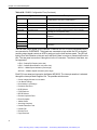
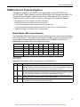
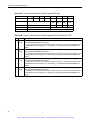
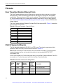
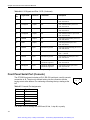
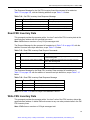
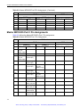
1
Artisan Technology Group is your source for quality new and certified-used/pre-owned equipment • FAST SHIPPING AND DELIVERY • TENS OF THOUSANDS OF IN-STOCK ITEMS • EQUIPMENT DEMOS • HUNDREDS OF MANUFACTURERS SUPPORTED • LEASING/MONTHLY RENTALS • ITAR CERTIFIED SECURE ASSET SOLUTIONS SERVICE CENTER REPAIRS Experienced engineers and technicians on staff at our full-service, in-house repair center WE BUY USED EQUIPMENT Sell your excess, underutilized, and idle used equipment We also offer credit for buy-backs and trade-ins www.artisantg.com/WeBuyEquipment InstraView REMOTE INSPECTION LOOKING FOR MORE INFORMATION? Visit us on the web at www.artisantg.com for more information on price quotations, drivers, technical specifications, manuals, and documentation SM Remotely inspect equipment before purchasing with our interactive website at www.instraview.com Contact us: (888) 88-SOURCE | [email protected] | www.artisantg.com CPC358 Octal Synchronous Serial Communications Processor Hardware Manual Performance Technologies 205 Indigo Creek Drive Rochester, NY 14626 USA 585.256.0248 [email protected] www.pt.com © 2009 Performance Technologies, Inc. All Rights Reserved. Artisan Technology Group - Quality Instrumentation ... Guaranteed | (888) 88-SOURCE | www.artisantg.com Document Revision History Part Number Date Explanation of changes 126P042710 08/01/03 Initial Production Release 126P042711 11/18/03 Certification Modifications 126P042712 08/18/04 Modification to RS-232C tables in Pinout and Rear Transition Modules Chapter 126P042713 03/11/09 Updated format. Added to jumper K5 description. 126P042714 04/29/09 Updated Table 6-4, “EIA-530 Connector Pin Assignments,” on page 132, to add cable shield description. Copyright Notice © Copyright 2003-2009 Performance Technologies, Inc. All Rights Reserved. The Performance Technologies logo is a registered trademark of Performance Technologies, Inc. All product and brand names may be trademarks or registered trademarks of their respective owners. This document is the sole property of Performance Technologies, Inc. Errors and Omissions Although diligent efforts are made to supply accurate technical information to the user, occasionally errors and omissions occur in manuals of this type. Refer to the Performance Technologies, Inc. web site to obtain manual revisions or current customer information: http://www.pt.com. Performance Technologies, Inc., reserves its right to change product specifications without notice. Symbol Conventions in This Manual The following symbols appear in this document: Caution: There is risk of equipment damage. Follow the instructions. Warning: Hazardous voltages are present. To reduce the risk of electrical shock and danger to personal health, follow the instructions. Caution: Electronic components on printed circuit boards are extremely sensitive to static electricity. Ordinary amounts of static electricity generated by your clothing or work environment can damage the electronic equipment. It is recommended that anti-static ground straps and antistatic mats are used when installing the board in a system to help prevent damage due to electrostatic discharge. Additional safety information is available throughout this guide and in the topic “Safety Precautions” on page 183. 2 Artisan Technology Group - Quality Instrumentation ... Guaranteed | (888) 88-SOURCE | www.artisantg.com Contents Chapter 1: About This Guide 19 Overview . . . . . . . . . . . . . . . . . . . . . . . . . . . . . . . . . . . . . . . . . . . . . . . . . . . . . . . . . . . . . . . . . . 19 Additional Documentation . . . . . . . . . . . . . . . . . . . . . . . . . . . . . . . . . . . . . . . . . . . . . . . . . . . . . 20 Text Conventions . . . . . . . . . . . . . . . . . . . . . . . . . . . . . . . . . . . . . . . . . . . . . . . . . . . . . . . . . . . 22 Customer Support and Services . . . . . . . . . . . . . . . . . . . . . . . . . . . . . . . . . . . . . . . . . . . . . . . . 22 Customer Support Packages . . . . . . . . . . . . . . . . . . . . . . . . . . . . . . . . . . . . . . . . . . . . . . . 23 Other Web Support . . . . . . . . . . . . . . . . . . . . . . . . . . . . . . . . . . . . . . . . . . . . . . . . . . . . . . . 23 Return Merchandise Authorization (RMA) . . . . . . . . . . . . . . . . . . . . . . . . . . . . . . . . . . . . . 23 Product Warranty . . . . . . . . . . . . . . . . . . . . . . . . . . . . . . . . . . . . . . . . . . . . . . . . . . . . . . . . . . . 23 Chapter 2: Introduction 25 Product Description . . . . . . . . . . . . . . . . . . . . . . . . . . . . . . . . . . . . . . . . . . . . . . . . . . . . . . . . . . 25 Features of the CPC358 . . . . . . . . . . . . . . . . . . . . . . . . . . . . . . . . . . . . . . . . . . . . . . . . . . . . . . 26 Rear Transition Module Features . . . . . . . . . . . . . . . . . . . . . . . . . . . . . . . . . . . . . . . . . . . . 27 CPC358 Architecture Overview . . . . . . . . . . . . . . . . . . . . . . . . . . . . . . . . . . . . . . . . . . . . . . . . 27 Processors . . . . . . . . . . . . . . . . . . . . . . . . . . . . . . . . . . . . . . . . . . . . . . . . . . . . . . . . . . . . . 27 Serial Communication Controllers . . . . . . . . . . . . . . . . . . . . . . . . . . . . . . . . . . . . . . . . . . . 27 Ethernet Ports . . . . . . . . . . . . . . . . . . . . . . . . . . . . . . . . . . . . . . . . . . . . . . . . . . . . . . . . . . . 28 Selectable Line Interface . . . . . . . . . . . . . . . . . . . . . . . . . . . . . . . . . . . . . . . . . . . . . . . . . . 28 Clock Steering . . . . . . . . . . . . . . . . . . . . . . . . . . . . . . . . . . . . . . . . . . . . . . . . . . . . . . . . . . . 28 Monitor Port . . . . . . . . . . . . . . . . . . . . . . . . . . . . . . . . . . . . . . . . . . . . . . . . . . . . . . . . . . . . 28 Electrical . . . . . . . . . . . . . . . . . . . . . . . . . . . . . . . . . . . . . . . . . . . . . . . . . . . . . . . . . . . . . . . 28 3 Artisan Technology Group - Quality Instrumentation ... Guaranteed | (888) 88-SOURCE | www.artisantg.com Contents Universal I/O . . . . . . . . . . . . . . . . . . . . . . . . . . . . . . . . . . . . . . . . . . . . . . . . . . . . . . . . . . . . 28 Media Connections . . . . . . . . . . . . . . . . . . . . . . . . . . . . . . . . . . . . . . . . . . . . . . . . . . . . . . . 28 Rear Transition Module Options . . . . . . . . . . . . . . . . . . . . . . . . . . . . . . . . . . . . . . . . . . . . . 29 Battery . . . . . . . . . . . . . . . . . . . . . . . . . . . . . . . . . . . . . . . . . . . . . . . . . . . . . . . . . . . . . . . . . 29 Mechanical . . . . . . . . . . . . . . . . . . . . . . . . . . . . . . . . . . . . . . . . . . . . . . . . . . . . . . . . . . . . . 29 Form Factor . . . . . . . . . . . . . . . . . . . . . . . . . . . . . . . . . . . . . . . . . . . . . . . . . . . . . . . . . . . . 29 CompactPCI Connectors . . . . . . . . . . . . . . . . . . . . . . . . . . . . . . . . . . . . . . . . . . . . . . . . . . 29 Front Panel . . . . . . . . . . . . . . . . . . . . . . . . . . . . . . . . . . . . . . . . . . . . . . . . . . . . . . . . . . . . . 30 CompactPCI Interface . . . . . . . . . . . . . . . . . . . . . . . . . . . . . . . . . . . . . . . . . . . . . . . . . . . . . . . . 30 Ethernet Ports . . . . . . . . . . . . . . . . . . . . . . . . . . . . . . . . . . . . . . . . . . . . . . . . . . . . . . . . . . . . . . 30 Ethernet PHY . . . . . . . . . . . . . . . . . . . . . . . . . . . . . . . . . . . . . . . . . . . . . . . . . . . . . . . . . . . 30 Ethernet MII Management . . . . . . . . . . . . . . . . . . . . . . . . . . . . . . . . . . . . . . . . . . . . . . . . . 30 Ethernet Status Indicators . . . . . . . . . . . . . . . . . . . . . . . . . . . . . . . . . . . . . . . . . . . . . . . . . . 30 Diagnostic Facilities . . . . . . . . . . . . . . . . . . . . . . . . . . . . . . . . . . . . . . . . . . . . . . . . . . . . . . . . . 30 Power-On Confidence (POC) . . . . . . . . . . . . . . . . . . . . . . . . . . . . . . . . . . . . . . . . . . . . . . . 31 Model Designations . . . . . . . . . . . . . . . . . . . . . . . . . . . . . . . . . . . . . . . . . . . . . . . . . . . . . . . . . 31 Chapter 3: Installation 33 Working with the CPC358 . . . . . . . . . . . . . . . . . . . . . . . . . . . . . . . . . . . . . . . . . . . . . . . . . . . . . 33 Installing the CPC358 . . . . . . . . . . . . . . . . . . . . . . . . . . . . . . . . . . . . . . . . . . . . . . . . . . . . . 33 Removing the CPC358 . . . . . . . . . . . . . . . . . . . . . . . . . . . . . . . . . . . . . . . . . . . . . . . . . . . . 34 LEDs . . . . . . . . . . . . . . . . . . . . . . . . . . . . . . . . . . . . . . . . . . . . . . . . . . . . . . . . . . . . . . . . . . 35 Jumpers and DIP Switches . . . . . . . . . . . . . . . . . . . . . . . . . . . . . . . . . . . . . . . . . . . . . . . . . . . . 38 Switch SW1 . . . . . . . . . . . . . . . . . . . . . . . . . . . . . . . . . . . . . . . . . . . . . . . . . . . . . . . . . . . . . 38 Jumpers . . . . . . . . . . . . . . . . . . . . . . . . . . . . . . . . . . . . . . . . . . . . . . . . . . . . . . . . . . . . . . . 38 Rear Transition Module Ethernet Routing and Ground . . . . . . . . . . . . . . . . . . . . . . . . . . . . 41 Reset and Abort . . . . . . . . . . . . . . . . . . . . . . . . . . . . . . . . . . . . . . . . . . . . . . . . . . . . . . . . . 42 Chapter 4: Functional Description 43 Power Distribution . . . . . . . . . . . . . . . . . . . . . . . . . . . . . . . . . . . . . . . . . . . . . . . . . . . . . . . . . . . 44 Reset Logic . . . . . . . . . . . . . . . . . . . . . . . . . . . . . . . . . . . . . . . . . . . . . . . . . . . . . . . . . . . . . . . . 46 Power On Reset . . . . . . . . . . . . . . . . . . . . . . . . . . . . . . . . . . . . . . . . . . . . . . . . . . . . . . . . . 46 4 Artisan Technology Group - Quality Instrumentation ... Guaranteed | (888) 88-SOURCE | www.artisantg.com Contents Hard Reset . . . . . . . . . . . . . . . . . . . . . . . . . . . . . . . . . . . . . . . . . . . . . . . . . . . . . . . . . . . . . 46 Soft Reset . . . . . . . . . . . . . . . . . . . . . . . . . . . . . . . . . . . . . . . . . . . . . . . . . . . . . . . . . . . . . . 47 Tundra PowerSpan Resets . . . . . . . . . . . . . . . . . . . . . . . . . . . . . . . . . . . . . . . . . . . . . . . . . 47 Peripheral Resets . . . . . . . . . . . . . . . . . . . . . . . . . . . . . . . . . . . . . . . . . . . . . . . . . . . . . . . . 48 General CPU Section . . . . . . . . . . . . . . . . . . . . . . . . . . . . . . . . . . . . . . . . . . . . . . . . . . . . . . . . 48 Master MPC8255 Initial Configuration . . . . . . . . . . . . . . . . . . . . . . . . . . . . . . . . . . . . . . . . 48 Master MPC8255 Internal Initial Configuration . . . . . . . . . . . . . . . . . . . . . . . . . . . . . . . . . . 50 Slave MPC8255 Initial Configuration . . . . . . . . . . . . . . . . . . . . . . . . . . . . . . . . . . . . . . . . . 51 Slave MPC8255 Internal Initial Configuration . . . . . . . . . . . . . . . . . . . . . . . . . . . . . . . . . . . 53 Master MPC8255 Memory Map . . . . . . . . . . . . . . . . . . . . . . . . . . . . . . . . . . . . . . . . . . . . . 53 Slave MPC8255 Memory Map . . . . . . . . . . . . . . . . . . . . . . . . . . . . . . . . . . . . . . . . . . . . . . 54 60x Bus Connections . . . . . . . . . . . . . . . . . . . . . . . . . . . . . . . . . . . . . . . . . . . . . . . . . . . . . 55 Master MPC8255 Interrupt Sources . . . . . . . . . . . . . . . . . . . . . . . . . . . . . . . . . . . . . . . . . . 55 Slave MPC8255 Interrupt Sources . . . . . . . . . . . . . . . . . . . . . . . . . . . . . . . . . . . . . . . . . . . 56 Master MPC8255 Local Bus Connections . . . . . . . . . . . . . . . . . . . . . . . . . . . . . . . . . . . . . 56 Slave MPC8255 Local Bus Connections (Unsupported Option) . . . . . . . . . . . . . . . . . . . . . 56 Master MPC8255 Parallel I/O Ports . . . . . . . . . . . . . . . . . . . . . . . . . . . . . . . . . . . . . . . . . . 57 Slave MPC8255 Parallel I/O Ports . . . . . . . . . . . . . . . . . . . . . . . . . . . . . . . . . . . . . . . . . . . 59 SDRAM . . . . . . . . . . . . . . . . . . . . . . . . . . . . . . . . . . . . . . . . . . . . . . . . . . . . . . . . . . . . . . . . . . . 59 External Master Support . . . . . . . . . . . . . . . . . . . . . . . . . . . . . . . . . . . . . . . . . . . . . . . . . . . 61 SDRAM Controller Initialization . . . . . . . . . . . . . . . . . . . . . . . . . . . . . . . . . . . . . . . . . . . . . . 62 Boot Flash Memory . . . . . . . . . . . . . . . . . . . . . . . . . . . . . . . . . . . . . . . . . . . . . . . . . . . . . . . . . . 63 Master MPC8255 Related Flash Settings . . . . . . . . . . . . . . . . . . . . . . . . . . . . . . . . . . . . . . 64 General Boot Flash Information . . . . . . . . . . . . . . . . . . . . . . . . . . . . . . . . . . . . . . . . . . . . . 64 Application Flash Memory . . . . . . . . . . . . . . . . . . . . . . . . . . . . . . . . . . . . . . . . . . . . . . . . . . . . . 65 Master MPC8255 Related Flash Settings . . . . . . . . . . . . . . . . . . . . . . . . . . . . . . . . . . . . . . 66 General Application Flash Information . . . . . . . . . . . . . . . . . . . . . . . . . . . . . . . . . . . . . . . . 67 Time of Day Timer . . . . . . . . . . . . . . . . . . . . . . . . . . . . . . . . . . . . . . . . . . . . . . . . . . . . . . . . . . 67 MPC8255 Related TOD Settings . . . . . . . . . . . . . . . . . . . . . . . . . . . . . . . . . . . . . . . . . . . . 68 General TOD Information . . . . . . . . . . . . . . . . . . . . . . . . . . . . . . . . . . . . . . . . . . . . . . . . . . 68 Communications Buffer Memory . . . . . . . . . . . . . . . . . . . . . . . . . . . . . . . . . . . . . . . . . . . . . . . . 69 MPC8255 Related Communications Buffer Memory Settings . . . . . . . . . . . . . . . . . . . . . . 70 UPMB Table Settings . . . . . . . . . . . . . . . . . . . . . . . . . . . . . . . . . . . . . . . . . . . . . . . . . . . . . 71 5 Artisan Technology Group - Quality Instrumentation ... Guaranteed | (888) 88-SOURCE | www.artisantg.com Contents CompactPCI Interface . . . . . . . . . . . . . . . . . . . . . . . . . . . . . . . . . . . . . . . . . . . . . . . . . . . . . . . . 71 PowerSpan Signal Connections and Hardware Configuration . . . . . . . . . . . . . . . . . . . . . . 71 PowerSpan Reset Configuration Word . . . . . . . . . . . . . . . . . . . . . . . . . . . . . . . . . . . . . . . . 72 PCI Device and Vendor ID . . . . . . . . . . . . . . . . . . . . . . . . . . . . . . . . . . . . . . . . . . . . . . . . . 73 Local 60x Bus Connections to the PowerSpan . . . . . . . . . . . . . . . . . . . . . . . . . . . . . . . . . . 73 PowerSpan Interrupts . . . . . . . . . . . . . . . . . . . . . . . . . . . . . . . . . . . . . . . . . . . . . . . . . . . . . 74 Fast Ethernet Controller . . . . . . . . . . . . . . . . . . . . . . . . . . . . . . . . . . . . . . . . . . . . . . . . . . . . . . 74 Serial I/O Interface . . . . . . . . . . . . . . . . . . . . . . . . . . . . . . . . . . . . . . . . . . . . . . . . . . . . . . . . . . 77 Clock Steering . . . . . . . . . . . . . . . . . . . . . . . . . . . . . . . . . . . . . . . . . . . . . . . . . . . . . . . . . . . 79 DTE / DCE Control . . . . . . . . . . . . . . . . . . . . . . . . . . . . . . . . . . . . . . . . . . . . . . . . . . . . . . . 80 General Purpose Registers . . . . . . . . . . . . . . . . . . . . . . . . . . . . . . . . . . . . . . . . . . . . . . . . . . . . 81 PSM552 General Purpose Registers . . . . . . . . . . . . . . . . . . . . . . . . . . . . . . . . . . . . . . . . . 83 PSM553 General Purpose Registers . . . . . . . . . . . . . . . . . . . . . . . . . . . . . . . . . . . . . . . . . 91 PSM554 Port Control Registers . . . . . . . . . . . . . . . . . . . . . . . . . . . . . . . . . . . . . . . . . . . . . 93 System Management Bus . . . . . . . . . . . . . . . . . . . . . . . . . . . . . . . . . . . . . . . . . . . . . . . . . . . . 103 Chapter 5: Boot PROM and Forth Monitor 105 Boot PROM Initialization . . . . . . . . . . . . . . . . . . . . . . . . . . . . . . . . . . . . . . . . . . . . . . . . . . . . . 105 Reset Configuration . . . . . . . . . . . . . . . . . . . . . . . . . . . . . . . . . . . . . . . . . . . . . . . . . . . . . 105 MPC8255 Reset Configuration Word . . . . . . . . . . . . . . . . . . . . . . . . . . . . . . . . . . . . . . . . 105 Slave MPC8255 Rest Configuration Word . . . . . . . . . . . . . . . . . . . . . . . . . . . . . . . . . . . . 105 PowerSpan Reset Configuration Word . . . . . . . . . . . . . . . . . . . . . . . . . . . . . . . . . . . . . . . 106 Bootup and Initialization . . . . . . . . . . . . . . . . . . . . . . . . . . . . . . . . . . . . . . . . . . . . . . . . . . 106 Hot-Swap/High Availability System Support . . . . . . . . . . . . . . . . . . . . . . . . . . . . . . . . . . . . . . 110 Resources Used by the Monitor . . . . . . . . . . . . . . . . . . . . . . . . . . . . . . . . . . . . . . . . . . . . . . . 110 Boot PROM . . . . . . . . . . . . . . . . . . . . . . . . . . . . . . . . . . . . . . . . . . . . . . . . . . . . . . . . . . . . 110 SDRAM . . . . . . . . . . . . . . . . . . . . . . . . . . . . . . . . . . . . . . . . . . . . . . . . . . . . . . . . . . . . . . . 110 Console Port . . . . . . . . . . . . . . . . . . . . . . . . . . . . . . . . . . . . . . . . . . . . . . . . . . . . . . . . . . . 110 Port C bit 4 . . . . . . . . . . . . . . . . . . . . . . . . . . . . . . . . . . . . . . . . . . . . . . . . . . . . . . . . . . . . 110 Power On Checks and POC Signature . . . . . . . . . . . . . . . . . . . . . . . . . . . . . . . . . . . . . . . 111 Host PCI Communication Interface . . . . . . . . . . . . . . . . . . . . . . . . . . . . . . . . . . . . . . . . . . 111 Soft Reset . . . . . . . . . . . . . . . . . . . . . . . . . . . . . . . . . . . . . . . . . . . . . . . . . . . . . . . . . . . . . 112 Forth Console . . . . . . . . . . . . . . . . . . . . . . . . . . . . . . . . . . . . . . . . . . . . . . . . . . . . . . . . . . 112 6 Artisan Technology Group - Quality Instrumentation ... Guaranteed | (888) 88-SOURCE | www.artisantg.com Contents Host PCI Interface Command Set . . . . . . . . . . . . . . . . . . . . . . . . . . . . . . . . . . . . . . . . . . . 115 Flash Error Codes . . . . . . . . . . . . . . . . . . . . . . . . . . . . . . . . . . . . . . . . . . . . . . . . . . . . . . . 117 Locally Resident Applications . . . . . . . . . . . . . . . . . . . . . . . . . . . . . . . . . . . . . . . . . . . . . . 117 Built-In Boot Sequence with Initialization from NVRAM . . . . . . . . . . . . . . . . . . . . . . . . . . 117 Chapter 6: Pinouts and Rear Transition Modules 123 Rear Transition Modules . . . . . . . . . . . . . . . . . . . . . . . . . . . . . . . . . . . . . . . . . . . . . . . . . . . . . 123 Pinouts . . . . . . . . . . . . . . . . . . . . . . . . . . . . . . . . . . . . . . . . . . . . . . . . . . . . . . . . . . . . . . . . . . 126 Rear Transition Module Ethernet Ports . . . . . . . . . . . . . . . . . . . . . . . . . . . . . . . . . . . . . . . 126 RS-232 Supported Signals . . . . . . . . . . . . . . . . . . . . . . . . . . . . . . . . . . . . . . . . . . . . . . . . 126 RS-449/422 Supported Signals . . . . . . . . . . . . . . . . . . . . . . . . . . . . . . . . . . . . . . . . . . . . 129 V.35 Supported Signals . . . . . . . . . . . . . . . . . . . . . . . . . . . . . . . . . . . . . . . . . . . . . . . . . . 135 Front Panel Serial Port (Console) . . . . . . . . . . . . . . . . . . . . . . . . . . . . . . . . . . . . . . . . . . . 142 Master MPC8255 JTAG Support . . . . . . . . . . . . . . . . . . . . . . . . . . . . . . . . . . . . . . . . . . . 143 Slave MPC8255 JTAG Support . . . . . . . . . . . . . . . . . . . . . . . . . . . . . . . . . . . . . . . . . . . . 143 Mictor Pinout . . . . . . . . . . . . . . . . . . . . . . . . . . . . . . . . . . . . . . . . . . . . . . . . . . . . . . . . . . . 144 CompactPCI Bus Connectors . . . . . . . . . . . . . . . . . . . . . . . . . . . . . . . . . . . . . . . . . . . . . . 146 Chapter 7: System Management Bus and Intelligent Platform Management 155 Overview of SMB . . . . . . . . . . . . . . . . . . . . . . . . . . . . . . . . . . . . . . . . . . . . . . . . . . . . . . . . . . 155 Intelligent Platform Management Interface (IPMI) . . . . . . . . . . . . . . . . . . . . . . . . . . . . . . . . . 155 Baseboard Management Controller . . . . . . . . . . . . . . . . . . . . . . . . . . . . . . . . . . . . . . . . . 156 Peripheral Management Controller . . . . . . . . . . . . . . . . . . . . . . . . . . . . . . . . . . . . . . . . . . 156 Intelligent Platform Management Bus (IPMB) . . . . . . . . . . . . . . . . . . . . . . . . . . . . . . . . . . 157 IPMB Compatibility . . . . . . . . . . . . . . . . . . . . . . . . . . . . . . . . . . . . . . . . . . . . . . . . . . . . . . 157 System-Side IPMI Management . . . . . . . . . . . . . . . . . . . . . . . . . . . . . . . . . . . . . . . . . . . . 157 IPMI Network Function Codes (netFn) . . . . . . . . . . . . . . . . . . . . . . . . . . . . . . . . . . . . . . . 158 Completion Codes . . . . . . . . . . . . . . . . . . . . . . . . . . . . . . . . . . . . . . . . . . . . . . . . . . . . . . 158 IPMI Commands Supported . . . . . . . . . . . . . . . . . . . . . . . . . . . . . . . . . . . . . . . . . . . . . . . 158 IPM Device Commands (netFn = 0x06, 0x07) . . . . . . . . . . . . . . . . . . . . . . . . . . . . . . . . . . . . 159 Common IPM Device Command Format . . . . . . . . . . . . . . . . . . . . . . . . . . . . . . . . . . . . . 159 Get Device ID . . . . . . . . . . . . . . . . . . . . . . . . . . . . . . . . . . . . . . . . . . . . . . . . . . . . . . . . . . 160 7 Artisan Technology Group - Quality Instrumentation ... Guaranteed | (888) 88-SOURCE | www.artisantg.com Contents Cold Reset . . . . . . . . . . . . . . . . . . . . . . . . . . . . . . . . . . . . . . . . . . . . . . . . . . . . . . . . . . . . 160 Warm Reset . . . . . . . . . . . . . . . . . . . . . . . . . . . . . . . . . . . . . . . . . . . . . . . . . . . . . . . . . . . 161 Set Manufacturing Test Mode ON . . . . . . . . . . . . . . . . . . . . . . . . . . . . . . . . . . . . . . . . . . 161 Get Self Test Results . . . . . . . . . . . . . . . . . . . . . . . . . . . . . . . . . . . . . . . . . . . . . . . . . . . . 161 Set ACPI Power State . . . . . . . . . . . . . . . . . . . . . . . . . . . . . . . . . . . . . . . . . . . . . . . . . . . . 161 Get ACPI Power State . . . . . . . . . . . . . . . . . . . . . . . . . . . . . . . . . . . . . . . . . . . . . . . . . . . 162 Get Device GUID . . . . . . . . . . . . . . . . . . . . . . . . . . . . . . . . . . . . . . . . . . . . . . . . . . . . . . . 162 Broadcast Get Device ID . . . . . . . . . . . . . . . . . . . . . . . . . . . . . . . . . . . . . . . . . . . . . . . . . 162 FRU Inventory Device Commands (netFn = 0x0A, 0x0B) . . . . . . . . . . . . . . . . . . . . . . . . . . . 163 Common FRU Inventory Device Commands . . . . . . . . . . . . . . . . . . . . . . . . . . . . . . . . . . 163 Get FRU Inventory Area . . . . . . . . . . . . . . . . . . . . . . . . . . . . . . . . . . . . . . . . . . . . . . . . . . 164 Read FRU Inventory Data . . . . . . . . . . . . . . . . . . . . . . . . . . . . . . . . . . . . . . . . . . . . . . . . . 165 Write FRU Inventory Data . . . . . . . . . . . . . . . . . . . . . . . . . . . . . . . . . . . . . . . . . . . . . . . . . 165 OEM (Vendor Specific) Commands (netFn = 0x30, 0x31) . . . . . . . . . . . . . . . . . . . . . . . . . . . 166 Common OEM Commands . . . . . . . . . . . . . . . . . . . . . . . . . . . . . . . . . . . . . . . . . . . . . . . . 166 Diagnostic Echo . . . . . . . . . . . . . . . . . . . . . . . . . . . . . . . . . . . . . . . . . . . . . . . . . . . . . . . . 167 Get Card Power Status . . . . . . . . . . . . . . . . . . . . . . . . . . . . . . . . . . . . . . . . . . . . . . . . . . . 168 Set Card Power State . . . . . . . . . . . . . . . . . . . . . . . . . . . . . . . . . . . . . . . . . . . . . . . . . . . . 169 Get Card Power State . . . . . . . . . . . . . . . . . . . . . . . . . . . . . . . . . . . . . . . . . . . . . . . . . . . . 170 Chapter 8: MPC8255 Parallel Port Pin Utilization 171 Master MPC8255 I2C Bus . . . . . . . . . . . . . . . . . . . . . . . . . . . . . . . . . . . . . . . . . . . . . . . . . . . 171 Master MPC8255 Parallel Port Pin Assignments . . . . . . . . . . . . . . . . . . . . . . . . . . . . . . . . . . 171 Master MPC8255 Port A Pin Assignments . . . . . . . . . . . . . . . . . . . . . . . . . . . . . . . . . . . . 171 Master MPC8255 Port B Pin Assignments . . . . . . . . . . . . . . . . . . . . . . . . . . . . . . . . . . . . 173 Master MPC8255 Port C Pin Assignments . . . . . . . . . . . . . . . . . . . . . . . . . . . . . . . . . . . . 174 Master MPC8255 Port D Pin assignments . . . . . . . . . . . . . . . . . . . . . . . . . . . . . . . . . . . . 176 Slave MPC8255 Parallel Port Pin Assignments . . . . . . . . . . . . . . . . . . . . . . . . . . . . . . . . . . . 176 Slave MPC8255 Port A Pin assignments . . . . . . . . . . . . . . . . . . . . . . . . . . . . . . . . . . . . . 177 Slave MPC8255 Port B Pin assignments . . . . . . . . . . . . . . . . . . . . . . . . . . . . . . . . . . . . . 178 Slave MPC8255 Port C Pin Assignments . . . . . . . . . . . . . . . . . . . . . . . . . . . . . . . . . . . . . 179 Slave MPC8255 Port D Pin assignments . . . . . . . . . . . . . . . . . . . . . . . . . . . . . . . . . . . . . 181 8 Artisan Technology Group - Quality Instrumentation ... Guaranteed | (888) 88-SOURCE | www.artisantg.com Contents Chapter 9: Agency Approvals 183 Safety Precautions . . . . . . . . . . . . . . . . . . . . . . . . . . . . . . . . . . . . . . . . . . . . . . . . . . . . . . . . . 183 Certifications . . . . . . . . . . . . . . . . . . . . . . . . . . . . . . . . . . . . . . . . . . . . . . . . . . . . . . . . . . . . . . 184 FCC Notice . . . . . . . . . . . . . . . . . . . . . . . . . . . . . . . . . . . . . . . . . . . . . . . . . . . . . . . . . . . . 184 CE Notice . . . . . . . . . . . . . . . . . . . . . . . . . . . . . . . . . . . . . . . . . . . . . . . . . . . . . . . . . . . . . 184 Compliance with RoHS and WEEE Directives . . . . . . . . . . . . . . . . . . . . . . . . . . . . . . . . . . . . 185 Non-Performance Technologies Branded Products . . . . . . . . . . . . . . . . . . . . . . . . . . . . . . . . 185 9 Artisan Technology Group - Quality Instrumentation ... Guaranteed | (888) 88-SOURCE | www.artisantg.com Contents 10 Artisan Technology Group - Quality Instrumentation ... Guaranteed | (888) 88-SOURCE | www.artisantg.com Ta b l e s Table 1-1: Manufacturer Part Numbers . . . . . . . . . . . . . . . . . . . . . . . . . . . . . . . . . . . . . . . . . . . . . . 21 Table 2-1: CPC358 Model Numbers . . . . . . . . . . . . . . . . . . . . . . . . . . . . . . . . . . . . . . . . . . . . . . . . 31 Table 2-2: CPC358 Accessory Cables . . . . . . . . . . . . . . . . . . . . . . . . . . . . . . . . . . . . . . . . . . . . . . 31 Table 3-1: Jumpers . . . . . . . . . . . . . . . . . . . . . . . . . . . . . . . . . . . . . . . . . . . . . . . . . . . . . . . . . . . . . 38 Table 3-2: Routing Jumpers for Ethernet Port A . . . . . . . . . . . . . . . . . . . . . . . . . . . . . . . . . . . . . . . 41 Table 3-3: Routing Jumpers for Ethernet Port B . . . . . . . . . . . . . . . . . . . . . . . . . . . . . . . . . . . . . . . 41 Table 3-4: Rear Transition Module Ground . . . . . . . . . . . . . . . . . . . . . . . . . . . . . . . . . . . . . . . . . . . 42 Table 4-1: Preliminary Typical Board Power Consumption Estimates . . . . . . . . . . . . . . . . . . . . . . 44 Table 4-2: On Pin Control Sources . . . . . . . . . . . . . . . . . . . . . . . . . . . . . . . . . . . . . . . . . . . . . . . . . 45 Table 4-3: Local Voltages . . . . . . . . . . . . . . . . . . . . . . . . . . . . . . . . . . . . . . . . . . . . . . . . . . . . . . . . 45 Table 4-4: !PQ_HRESET Control Signals and Select Jumpers. . . . . . . . . . . . . . . . . . . . . . . . . . . . 46 Table 4-5: Peripheral Resets . . . . . . . . . . . . . . . . . . . . . . . . . . . . . . . . . . . . . . . . . . . . . . . . . . . . . . 48 Table 4-6: Master MPC8255 System Clock Control Register Bit Field Definitions . . . . . . . . . . . . . 49 Table 4-7: Master MPC8255 Hard Reset Configuration Word Settings . . . . . . . . . . . . . . . . . . . . . 49 Table 4-8: Master MPC8255 SIUMCR Register Settings . . . . . . . . . . . . . . . . . . . . . . . . . . . . . . . . 50 Table 4-9: Slave MPC8255 System Clock Control Register Bit Field Definitions . . . . . . . . . . . . . . 51 Table 4-10: Slave MPC8255 Hard Reset Configuration Word Settings . . . . . . . . . . . . . . . . . . . . . 52 Table 4-11: Slave MPC8255 SIUMCR Register Settings . . . . . . . . . . . . . . . . . . . . . . . . . . . . . . . . 53 11 Artisan Technology Group - Quality Instrumentation ... Guaranteed | (888) 88-SOURCE | www.artisantg.com Tables Table 4-12: Master MPC8255 Chip Select Assignments. . . . . . . . . . . . . . . . . . . . . . . . . . . . . . . . . 54 Table 4-13: Slave MPC8255 Chip Select Assignments. . . . . . . . . . . . . . . . . . . . . . . . . . . . . . . . . . 54 Table 4-14: Master MPC8255 Interrupt Sources . . . . . . . . . . . . . . . . . . . . . . . . . . . . . . . . . . . . . . . 55 Table 4-15: CS0 Base Register Settings . . . . . . . . . . . . . . . . . . . . . . . . . . . . . . . . . . . . . . . . . . . . . 64 Table 4-16: CS0 Option Register Settings. . . . . . . . . . . . . . . . . . . . . . . . . . . . . . . . . . . . . . . . . . . . 64 Table 4-17: CS3 Base Register Settings . . . . . . . . . . . . . . . . . . . . . . . . . . . . . . . . . . . . . . . . . . . . . 66 Table 4-18: CS3 Option Register Settings. . . . . . . . . . . . . . . . . . . . . . . . . . . . . . . . . . . . . . . . . . . . 67 Table 4-19: CS8 Base Register Settings . . . . . . . . . . . . . . . . . . . . . . . . . . . . . . . . . . . . . . . . . . . . . 68 Table 4-20: CS8 Option Register Settings. . . . . . . . . . . . . . . . . . . . . . . . . . . . . . . . . . . . . . . . . . . . 68 Table 4-21: CS2 Base Register Settings . . . . . . . . . . . . . . . . . . . . . . . . . . . . . . . . . . . . . . . . . . . . . 70 Table 4-22: CS2 Option Register Settings. . . . . . . . . . . . . . . . . . . . . . . . . . . . . . . . . . . . . . . . . . . . 71 Table 4-23: Signal Variations From Between PowerSpan and the Master MPC8255. . . . . . . . . . . 73 Table 4-24: PowerSpan Reset Pins. . . . . . . . . . . . . . . . . . . . . . . . . . . . . . . . . . . . . . . . . . . . . . . . . 73 Table 4-25: PowerSpan Interrupt Connections . . . . . . . . . . . . . . . . . . . . . . . . . . . . . . . . . . . . . . . . 74 Table 4-26: CS8952 Configuration Pins . . . . . . . . . . . . . . . . . . . . . . . . . . . . . . . . . . . . . . . . . . . . . 75 Table 4-27: V.35 DTE / DCE Signal Continuity . . . . . . . . . . . . . . . . . . . . . . . . . . . . . . . . . . . . . . . . 80 Table 4-28: CS4 Base Register Settings . . . . . . . . . . . . . . . . . . . . . . . . . . . . . . . . . . . . . . . . . . . . . 82 Table 4-29: CS4 Option Register Settings. . . . . . . . . . . . . . . . . . . . . . . . . . . . . . . . . . . . . . . . . . . . 82 Table 4-30: Peripheral Reset Control Register Bit Fields . . . . . . . . . . . . . . . . . . . . . . . . . . . . . . . . 83 Table 4-31: Peripheral Reset Control Register Bit Field Definitions . . . . . . . . . . . . . . . . . . . . . . . . 84 Table 4-32: Ejector Switch Interrupt Enable Control Register Bit Fields . . . . . . . . . . . . . . . . . . . . . 84 Table 4-33: Ejector Switch Interrupt Enable Control Register Bit Field Definitions . . . . . . . . . . . . . 84 Table 4-34: Ejector Switch Interrupt Status Register Bit Field Definitions . . . . . . . . . . . . . . . . . . . . 85 Table 4-35: Ejector Switch Interrupt Status Register Bit Field Definitions . . . . . . . . . . . . . . . . . . . . 85 Table 4-36: Miscellaneous Status and Control Register Bit Fields . . . . . . . . . . . . . . . . . . . . . . . . . 85 Table 4-37: Miscellaneous Status and Control Register Bit Field Definitions . . . . . . . . . . . . . . . . . 86 12 Artisan Technology Group - Quality Instrumentation ... Guaranteed | (888) 88-SOURCE | www.artisantg.com Tables Table 4-38: General Purpose Latch Register Bit Fields . . . . . . . . . . . . . . . . . . . . . . . . . . . . . . . . . 87 Table 4-39: Register Bit Field Definitions . . . . . . . . . . . . . . . . . . . . . . . . . . . . . . . . . . . . . . . . . . . . 87 Table 4-40: General Purpose Switch and P1 Reset Register Bit Fields . . . . . . . . . . . . . . . . . . . . . 87 Table 4-41: General Purpose Switch and P1 Reset Register Bit Field Definitions . . . . . . . . . . . . . 87 Table 4-42: P1 Reset Control Register Bit Fields . . . . . . . . . . . . . . . . . . . . . . . . . . . . . . . . . . . . . . 88 Table 4-43: P1 Reset Control Register Bit Field Definitions . . . . . . . . . . . . . . . . . . . . . . . . . . . . . . 88 Table 4-44: Hot Swap Status and Control Register Bit Fields . . . . . . . . . . . . . . . . . . . . . . . . . . . . . 88 Table 4-45: Hot Swap Status and Control Register Bit Field Definitions . . . . . . . . . . . . . . . . . . . . . 89 Table 4-46: Board ID Register 1 Bit Fields . . . . . . . . . . . . . . . . . . . . . . . . . . . . . . . . . . . . . . . . . . . 90 Table 4-47: Board ID Register 1 Bit Field Definitions . . . . . . . . . . . . . . . . . . . . . . . . . . . . . . . . . . . 90 Table 4-48: Board ID Register 2 Bit Fields . . . . . . . . . . . . . . . . . . . . . . . . . . . . . . . . . . . . . . . . . . . 90 Table 4-49: Board ID Register 2 Bit Field Definitions . . . . . . . . . . . . . . . . . . . . . . . . . . . . . . . . . . . 90 Table 4-50: Board Status LED Control Register Bit Fields . . . . . . . . . . . . . . . . . . . . . . . . . . . . . . . 91 Table 4-51: Board Status LED Control Register Bit Field Definitions . . . . . . . . . . . . . . . . . . . . . . . 91 Table 4-52: Compact PCI Geographic Address Register Bit Fields . . . . . . . . . . . . . . . . . . . . . . . . 92 Table 4-53: Compact PCI Geographic Address Register Bit Field Definitions . . . . . . . . . . . . . . . . 92 Table 4-54: CT Bus Shelf Address Register Bit Fields . . . . . . . . . . . . . . . . . . . . . . . . . . . . . . . . . . 92 Table 4-55: CT Bus Shelf Address Register Bit Field Definitions . . . . . . . . . . . . . . . . . . . . . . . . . . 92 Table 4-56: Transceiver Mode Control Selection Bits . . . . . . . . . . . . . . . . . . . . . . . . . . . . . . . . . . . 95 Table 4-57: Transceiver 1-2 (5-6) Mode Control Register Bit Fields . . . . . . . . . . . . . . . . . . . . . . . . 95 Table 4-58: Transceiver 1-2 (5-6) Mode Control Register Bit Field Definitions . . . . . . . . . . . . . . . . 95 Table 4-59: Transceiver 3-4 (7-8) Mode Control Register Bit Fields . . . . . . . . . . . . . . . . . . . . . . . . 96 Table 4-60: Transceiver 3-4 (7-8) Mode Control Register Bit Field Definitions . . . . . . . . . . . . . . . . 96 Table 4-61: Receive Clock Steering Control Register Bit Fields . . . . . . . . . . . . . . . . . . . . . . . . . . . 97 Table 4-62: Receive Clock Steering Control Register Bit Field Definitions . . . . . . . . . . . . . . . . . . . 97 Table 4-63: Transmit Clock Steering Control Register Bit Fields . . . . . . . . . . . . . . . . . . . . . . . . . . 98 13 Artisan Technology Group - Quality Instrumentation ... Guaranteed | (888) 88-SOURCE | www.artisantg.com Tables Table 4-64: Transmit Clock Steering Control Register Bit Field Definitions - DTE . . . . . . . . . . . . . 98 Table 4-65: Transmit Clock Steering Control Register Bit Field Definitions - DCE . . . . . . . . . . . . . 99 Table 4-66: Port 1-2 (5-6) Status LED Control Register Bit Fields . . . . . . . . . . . . . . . . . . . . . . . . . 99 Table 4-67: Port 1-2 (5-6) Status LED Control Register Bit Field Definitions . . . . . . . . . . . . . . . . 100 Table 4-68: Port 3-4 (7-8) Status LED Control Register Bit Fields . . . . . . . . . . . . . . . . . . . . . . . . 100 Table 4-69: Port 3-4 (7-8) Status LED Control Register Bit Field Definitions . . . . . . . . . . . . . . . . 101 Table 4-70: Transceiver Shutdown Control Register Bit Fields . . . . . . . . . . . . . . . . . . . . . . . . . . . 101 Table 4-71: Transceiver Shutdown Control Register Bit Field Definitions . . . . . . . . . . . . . . . . . . . 101 Table 4-72: LED Mode/Slave Reset Control Register Bit Fields . . . . . . . . . . . . . . . . . . . . . . . . . 102 Table 4-73: LED Mode/Slave Reset Control Register Bit Field Definitions . . . . . . . . . . . . . . . . . . 102 Table 4-74: CompactPCI SMB to CPC358 SMB Interface . . . . . . . . . . . . . . . . . . . . . . . . . . . . . . 103 Table 5-1: POC Signature . . . . . . . . . . . . . . . . . . . . . . . . . . . . . . . . . . . . . . . . . . . . . . . . . . . . . . . 111 Table 5-2: Flash Error Codes . . . . . . . . . . . . . . . . . . . . . . . . . . . . . . . . . . . . . . . . . . . . . . . . . . . . 117 Table 5-3: NVRAM Structure . . . . . . . . . . . . . . . . . . . . . . . . . . . . . . . . . . . . . . . . . . . . . . . . . . . . . 118 Table 6-1: Ethernet Connector J3 and J4 Pinout. . . . . . . . . . . . . . . . . . . . . . . . . . . . . . . . . . . . . . 126 Table 6-2: RS-232C Connector Pin Assignments . . . . . . . . . . . . . . . . . . . . . . . . . . . . . . . . . . . . . 126 Table 6-3: RS-449 Connector Pin Assignments . . . . . . . . . . . . . . . . . . . . . . . . . . . . . . . . . . . . . . 129 Table 6-4: EIA-530 Connector Pin Assignments . . . . . . . . . . . . . . . . . . . . . . . . . . . . . . . . . . . . . 132 Table 6-5: V.35 Connector Pin Assignments . . . . . . . . . . . . . . . . . . . . . . . . . . . . . . . . . . . . . . . . 136 Table 6-6: V.35 Signals and Pins - DCE . . . . . . . . . . . . . . . . . . . . . . . . . . . . . . . . . . . . . . . . . . . . 138 Table 6-7: Console Pin Assignments. . . . . . . . . . . . . . . . . . . . . . . . . . . . . . . . . . . . . . . . . . . . . . . 142 Table 6-8: Master JTAG Pinout . . . . . . . . . . . . . . . . . . . . . . . . . . . . . . . . . . . . . . . . . . . . . . . . . . . 143 Table 6-9: Slave JTAG Pinout . . . . . . . . . . . . . . . . . . . . . . . . . . . . . . . . . . . . . . . . . . . . . . . . . . . . 143 Table 6-10: J9 Mictor Pinout, 60X Bus Address . . . . . . . . . . . . . . . . . . . . . . . . . . . . . . . . . . . . . . 144 Table 6-11: J10 Mictor Pinout, 60X Bux Data . . . . . . . . . . . . . . . . . . . . . . . . . . . . . . . . . . . . . . . . 145 Table 6-12: J11 Mictor Pinout, 60X Bus Data . . . . . . . . . . . . . . . . . . . . . . . . . . . . . . . . . . . . . . . . 145 14 Artisan Technology Group - Quality Instrumentation ... Guaranteed | (888) 88-SOURCE | www.artisantg.com Tables Table 6-13: J1 CompactPCI Connections . . . . . . . . . . . . . . . . . . . . . . . . . . . . . . . . . . . . . . . . . . . 147 Table 6-14: J2 CompactPCI Connections . . . . . . . . . . . . . . . . . . . . . . . . . . . . . . . . . . . . . . . . . . . 148 Table 6-15: J3 RS-422, RS449, RS-530 Signal pinouts . . . . . . . . . . . . . . . . . . . . . . . . . . . . . . . . 149 Table 6-16: DTE RS232 Adjustments for J3 . . . . . . . . . . . . . . . . . . . . . . . . . . . . . . . . . . . . . . . . . 150 Table 6-17: DTE V.35 Adjustments for J3 . . . . . . . . . . . . . . . . . . . . . . . . . . . . . . . . . . . . . . . . . . . 150 Table 6-18: J4 CompactPCI Connections . . . . . . . . . . . . . . . . . . . . . . . . . . . . . . . . . . . . . . . . . . . 151 Table 6-19: J5 RS-422, RS-449,RS-530 Signal Pinouts . . . . . . . . . . . . . . . . . . . . . . . . . . . . . . . 152 Table 6-20: DTE RS232 Adjustments for J5 . . . . . . . . . . . . . . . . . . . . . . . . . . . . . . . . . . . . . . . . . 153 Table 6-21: DTE V.35 Adjustments for J5 . . . . . . . . . . . . . . . . . . . . . . . . . . . . . . . . . . . . . . . . . . . 153 Table 7-1: IPMB Slave Address Map . . . . . . . . . . . . . . . . . . . . . . . . . . . . . . . . . . . . . . . . . . . . . . 157 Table 7-2: Supported Network Function Codes . . . . . . . . . . . . . . . . . . . . . . . . . . . . . . . . . . . . . . 158 Table 7-3: IPM Device Request (Commands) Message Format . . . . . . . . . . . . . . . . . . . . . . . . . 159 Table 7-4: IPM Device Response Message Format . . . . . . . . . . . . . . . . . . . . . . . . . . . . . . . . . . . 159 Table 7-5: Get Device ID Response Message . . . . . . . . . . . . . . . . . . . . . . . . . . . . . . . . . . . . . . . 160 Table 7-6: Get Self Test Results Response Message . . . . . . . . . . . . . . . . . . . . . . . . . . . . . . . . . 161 Table 7-7: Set ACPI Power State Request Message . . . . . . . . . . . . . . . . . . . . . . . . . . . . . . . . . . 162 Table 7-8: Get ACPI Power State Response Message . . . . . . . . . . . . . . . . . . . . . . . . . . . . . . . . 162 Table 7-9: Broadcast Get Device IP Request Message . . . . . . . . . . . . . . . . . . . . . . . . . . . . . . . . 163 Table 7-10: FRU Inventory Device Request Formats . . . . . . . . . . . . . . . . . . . . . . . . . . . . . . . . . . 163 Table 7-12: FRU Inventory Layout . . . . . . . . . . . . . . . . . . . . . . . . . . . . . . . . . . . . . . . . . . . . . . . . 164 Table 7-13: Get FRU Inventory Area Request Commands . . . . . . . . . . . . . . . . . . . . . . . . . . . . . 164 Table 7-11: FRU Inventory Device Response Formats . . . . . . . . . . . . . . . . . . . . . . . . . . . . . . . . 164 Table 7-14: Get FRU Inventory Area Response Message . . . . . . . . . . . . . . . . . . . . . . . . . . . . . . 165 Table 7-15: Read FRU Inventory Data Request Commands . . . . . . . . . . . . . . . . . . . . . . . . . . . . 165 Table 7-16: Read FRU Inventory Data Response Message . . . . . . . . . . . . . . . . . . . . . . . . . . . . 165 Table 7-17: Write FRU Inventory Data Request Commands. . . . . . . . . . . . . . . . . . . . . . . . . . . . 166 15 Artisan Technology Group - Quality Instrumentation ... Guaranteed | (888) 88-SOURCE | www.artisantg.com Tables Table 7-18: Write FRU Inventory Data Response Message . . . . . . . . . . . . . . . . . . . . . . . . . . . . 166 Table 7-19: Common OEM Request Commands . . . . . . . . . . . . . . . . . . . . . . . . . . . . . . . . . . . . . 167 Table 7-20: Common OEM Response Commands . . . . . . . . . . . . . . . . . . . . . . . . . . . . . . . . . . . 167 Table 7-21: Diagnostic Echo Request Commands . . . . . . . . . . . . . . . . . . . . . . . . . . . . . . . . . . . . 167 Table 7-22: Diagnostic Echo Response Message. . . . . . . . . . . . . . . . . . . . . . . . . . . . . . . . . . . . 168 Table 7-23: Bit Assignments for Card Power Status Byte . . . . . . . . . . . . . . . . . . . . . . . . . . . . . . 168 Table 7-24: Get Card Power Status Request Message . . . . . . . . . . . . . . . . . . . . . . . . . . . . . . . . 168 Table 7-25: Get Card Power Status Response Message. . . . . . . . . . . . . . . . . . . . . . . . . . . . . . . 169 Table 7-26: Bit Assignments for Card Power State Byte . . . . . . . . . . . . . . . . . . . . . . . . . . . . . . . 169 Table 7-27: Set Card Power State Request Message . . . . . . . . . . . . . . . . . . . . . . . . . . . . . . . . . 169 Table 7-28: Set Card Power State Response Message . . . . . . . . . . . . . . . . . . . . . . . . . . . . . . . . 170 Table 7-29: Get Card Power State Request Message . . . . . . . . . . . . . . . . . . . . . . . . . . . . . . . . . 170 Table 7-30: Get Card Power State Response Message. . . . . . . . . . . . . . . . . . . . . . . . . . . . . . . . 170 Table 8-1: Master MPC8255 Port A Pin Assignments . . . . . . . . . . . . . . . . . . . . . . . . . . . . . . . . . . 172 Table 8-2: Master MPC8255 Port B Pin Assignments . . . . . . . . . . . . . . . . . . . . . . . . . . . . . . . . . . 173 Table 8-3: Master MPC8255 Port C Pin Assignments. . . . . . . . . . . . . . . . . . . . . . . . . . . . . . . . . . 174 Table 8-4: Master MPC8255 Port D Pin Assignments. . . . . . . . . . . . . . . . . . . . . . . . . . . . . . . . . . 176 Table 8-5: Slave MPC8255 Port A Pin Assignments. . . . . . . . . . . . . . . . . . . . . . . . . . . . . . . . . . . 177 Table 8-6: Slave MPC8255 Port B Pin Assignments. . . . . . . . . . . . . . . . . . . . . . . . . . . . . . . . . . . 178 Table 8-7: Slave MPC8255 Port C Pin Assignments. . . . . . . . . . . . . . . . . . . . . . . . . . . . . . . . . . . 179 Table 8-8: Slave MPC8255 Port D Pin Assignments. . . . . . . . . . . . . . . . . . . . . . . . . . . . . . . . . . . 181 16 Artisan Technology Group - Quality Instrumentation ... Guaranteed | (888) 88-SOURCE | www.artisantg.com Figures Figure 3-1: CompactPCI Chassis . . . . . . . . . . . . . . . . . . . . . . . . . . . . . . . . . . . . . . . . . . . . . . . . . . 34 Figure 3-2: CPC358 Front Panel . . . . . . . . . . . . . . . . . . . . . . . . . . . . . . . . . . . . . . . . . . . . . . . . . . . 35 Figure 3-3: CPC358 Board Layout . . . . . . . . . . . . . . . . . . . . . . . . . . . . . . . . . . . . . . . . . . . . . . . . . 36 Figure 3-4: Additional Jumper Locations . . . . . . . . . . . . . . . . . . . . . . . . . . . . . . . . . . . . . . . . . . . . . 37 Figure 4-1: Block Diagram of CPC358 . . . . . . . . . . . . . . . . . . . . . . . . . . . . . . . . . . . . . . . . . . . . . . 44 Figure 4-2: Partial SDRAM State Diagram . . . . . . . . . . . . . . . . . . . . . . . . . . . . . . . . . . . . . . . . . . . 60 Figure 4-3: External Master SDRAM Configuration . . . . . . . . . . . . . . . . . . . . . . . . . . . . . . . . . . . . . 62 Figure 4-4: Flash Block Diagram . . . . . . . . . . . . . . . . . . . . . . . . . . . . . . . . . . . . . . . . . . . . . . . . . . . 63 Figure 4-5: Application Flash Block Diagram. . . . . . . . . . . . . . . . . . . . . . . . . . . . . . . . . . . . . . . . . . 66 Figure 4-6: TOD Block Diagram . . . . . . . . . . . . . . . . . . . . . . . . . . . . . . . . . . . . . . . . . . . . . . . . . . . 67 Figure 4-7: Communications Buffer Memory Block Diagram. . . . . . . . . . . . . . . . . . . . . . . . . . . . . . 69 Figure 4-8: Ethernet Dual PHY Block Diagram . . . . . . . . . . . . . . . . . . . . . . . . . . . . . . . . . . . . . . . . 75 Figure 4-9: Serial I/O Port Block Diagram . . . . . . . . . . . . . . . . . . . . . . . . . . . . . . . . . . . . . . . . . . . . 78 Figure 4-10: Clock Steering . . . . . . . . . . . . . . . . . . . . . . . . . . . . . . . . . . . . . . . . . . . . . . . . . . . . . . . 79 Figure 4-11: General Purpose Registers Block Diagram. . . . . . . . . . . . . . . . . . . . . . . . . . . . . . . . . 81 Figure 4-12: Port Control Registers Block Diagram. . . . . . . . . . . . . . . . . . . . . . . . . . . . . . . . . . . . . 94 Figure 5-1: Boot Flow Chart (part 1) . . . . . . . . . . . . . . . . . . . . . . . . . . . . . . . . . . . . . . . . . . . . . . . 121 Figure 5-2: Boot Flow Chart (part 2) . . . . . . . . . . . . . . . . . . . . . . . . . . . . . . . . . . . . . . . . . . . . . . . 122 17 Artisan Technology Group - Quality Instrumentation ... Guaranteed | (888) 88-SOURCE | www.artisantg.com Figures Figure 6-1: RTM Diagrams - Rear I/O . . . . . . . . . . . . . . . . . . . . . . . . . . . . . . . . . . . . . . . . . . . . . . 124 Figure 6-2: RTM Diagrams - Front I/O. . . . . . . . . . . . . . . . . . . . . . . . . . . . . . . . . . . . . . . . . . . . . . 125 Figure 7-1: CompactPCI SMB Block Diagram . . . . . . . . . . . . . . . . . . . . . . . . . . . . . . . . . . . . . . . . 156 18 Artisan Technology Group - Quality Instrumentation ... Guaranteed | (888) 88-SOURCE | www.artisantg.com Chapter 1 About This Guide Overview This manual describes the operation and use of the CPC358 Octal Synchronous Serial Communications Processor (referred to as the CPC358 in this guide). The following outline describes the focus of each chapter Chapter 2, “Introduction,” provides a quick summary of the CPC358 features. Chapter 3, “Installation,” includes diagrams of the CPC358, descriptions of jumper functions, and instructions for physical installation. Chapter 4, “Functional Description,” provides a detailed description of CPC358 architecture and functional blocks. Chapter 5, “Boot PROM and Forth Monitor,” provides information about the Forth monitor. Chapter 6, “Pinouts and Rear Transition Modules,” includes connector pinouts, and descriptions and diagrams of the available RTMs. Chapter 7, “System Management Bus and Intelligent Platform Management,” describes the System Management Bus. Chapter 8, “MPC8255 Parallel Port Pin Utilization,” presents pinouts of the MPC8255 parallel ports. Chapter 9, “Agency Approvals,” provides agency approval and certification information. 19 Artisan Technology Group - Quality Instrumentation ... Guaranteed | (888) 88-SOURCE | www.artisantg.com Chapter 1: About This Guide Additional Documentation This manual is not intended to be a stand-alone document. It is necessary to have a complete understanding of all the features and function of the hardware to adequately develop software for this product. Consult the following list of additional documentation for sources of further information. The most current documentation to support the additional components that you purchased from Performance Technologies is available at http://www.pt.com/ under the product you are inquiring about. • PICMG 2.16 Revision 1.0 CompactPCI Packet Switching Backplane Specification, Sept. 5, 2001 • PICMG 2.0 Revision 3.0 CompactPCI Core Specification, Oct. 1, 1999 • PICMG 2.1 Revision 2.0 Hot-Swap Specification, Jan. 17, 2001 • PICMG 2.9 Revision 1.0 System Management Specification, Feb. 2, 2000 • PCI Industrial Computer Manufacturer’s Group. More information at: http://www.picmg.org/ • IPMI Platform Management FRU Information Storage Definition V1.0 Document Revision 1.1, Sept. 27, 1999 Intel, Hewlett Packard, NEC, Dell Computer More information at: http://developer.intel.com/design/servers/ipmi/spec.htm/ • PowerQUICC II Users Manual MPC8260UM/D Rev.0 The CPC358 utilizes the Motorola MPC8255, which supports a subset of the MPC8260’s features. The MPC8255 does not have its own manual; please refer to the MPC8260 User’s Manual for information regarding the MPC8255. MPC8260UM/D, Rev 0 Motorola Incorporated, Motorola Literature Distribution Center, P.O.Box 5405, Denver, Colorado 80217, U.S.A. Tel: (800) 441-2447 More information at: http://e-www.motorola.com/webapp/sps/site/ prod_summary.jsp?code=MPC8260&nodeId=01M98657 • CA91L8260 Tundra PowerSpan Datasheet 20 Artisan Technology Group - Quality Instrumentation ... Guaranteed | (888) 88-SOURCE | www.artisantg.com Additional Documentation Tundra Semiconductor Corp. 603 March Rd., Kanata, Ontario, K2K 2M5, Canada Tel: 613-592-0714 More information at: http://www.tundra.com/page.cfm?tree_id=100008 Table 1-1: Manufacturer Part Numbers Part Part Number Manufacturer MPC8255 PowerQUICC II Communications Processor MPC8255AZUMHBB Motorola http://e-www.motorola.com CA91L8260 PowerSpan Single Port PCI Bridge CA91L8260-100CE Tundra Semiconductor Corp. 603 March Road Kanata, Ontario K2K 2M5 Canada Tel: 613-592-0714 PIC Microcontroller, 20 MHz PIC16F877-20/PQ Microchip Technology Inc. 2355 West Chandler Blvd. Chandler, AZ 85224-6199 USA Tel: 602-786-7200 4 Megabit (512 K x 8-Bit) CMOS 3.0 V-only Flash Memory AM29LV040B-90JC Advanced Micro Devices One AMD Place P.O. Box 3453 Sunnyvale, CA 94088-3453 USA Tel: 408-732-2400 3 V 128 Mbit StrataFlash Memory E28F128J3A-150 Intel Corp. http://www.intel.com SODIMM Memory 128 Mbyte 100 MHz MT4LSDT1664HG-10EB1 Micron Technology 8000 S. Federal Way PO Box 6 Boise, ID 83707-0006 USA Tel: 208-368-3900 SNAPHAT Battery, 49 MAH M4T28-BR12SH1 ST Microelectronics 1000 E. Bell Road Phoenix, AZ 85022 USA Tel: 602-485-6100 3.3V Software-Selectable Multiprotocol Transceiver LTC2844CG Linear Technology 1630 McCarthy Blvd. Milpitas, CA 95035-7417 USA Tel: 408-432-1900 3.3V Software-Selectable Multiprotocol Transceiver with Termination LTC2846CG Linear Technology 1630 McCarthy Blvd. Milpitas, CA 95035-7417 USA Tel: 408-432-1900 RS-232 Transmitter/Receiver ICL3221ECV Intersil Corp. 7585 Irvine Center Drive Suite 100 Irvine, CA 92618 USA Tel: 949-341-7000 21 Artisan Technology Group - Quality Instrumentation ... Guaranteed | (888) 88-SOURCE | www.artisantg.com Chapter 1: About This Guide Text Conventions Conventions in This Guide describes the text conventions that are used in this guide. Conventions in This Guide Convention Used For Monospace font Monospace font represents sample code. Bold font Bold font represents: • paths • file names • UNIX commands • user input. Italic font Italic font represents: • notes that supply useful advice • supplemental information • referenced documents. Customer Support and Services Performance Technologies offers a variety of standard and custom support packages to ensure customers have access to the critical resources that they need to protect and maximize hardware and software investments throughout the development, integration, and deployment phases of the product life cycle. If you encounter difficulty in using this Performance Technologies, Inc. product, you may contact our support personnel by: 1. EMAIL (Preferred Method) – Email us at the addresses listed below or use our online email support form. Outline your problem in detail. Please include your return email address and a telephone number. 2. TELEPHONE – Contact us via telephone at the number listed below, and request Technical Support. Our offices are open Monday to Friday, 8:00 a.m. to 8:00 p.m. (Eastern Standard Time). Performance Technologies Support Contact Information Embedded Systems and Software (Includes Platforms, Blades, and Servers) SS7 Systems (Includes SEGway™) Email [email protected] [email protected] Phone +1 (585) 256-0248 (Monday to Friday, 8 a.m. to 8 p.m. Eastern Standard Time) +1 (585) 256-0248 (Monday to Friday, 8 a.m. to 8 p.m. Eastern Standard Time) If you are located outside North America, we encourage you to contact the local Performance Technologies’ distributor or agent for support. Many of our distributors or agents maintain technical support staffs. 22 Artisan Technology Group - Quality Instrumentation ... Guaranteed | (888) 88-SOURCE | www.artisantg.com Product Warranty Customer Support Packages Our configurable development and integration support packages help customers maximize engineering efforts and achieve time-to-market goals. To find out more about our Customer Support packages, visit http://www.pt.com/page/support/. Other Web Support Support for existing products including manuals, release notes, and drivers can be found on specific product pages at http://www.pt.com. Use the product search to locate the information you need. Return Merchandise Authorization (RMA) To submit a return merchandise authorization (RMA) request, complete the online RMA form available at http://pt.com/assets/lib/files/rma-request-form.doc and follow the instructions on the form. You will be notified with an RMA number once your return request is approved. Shipping information for returning the unit to Performance Technologies will be provided once the RMA is issued. Product Warranty Performance Technologies, Incorporated, warrants that its products sold hereunder will at the time of shipment be free from defects in material and workmanship and will conform to Performance Technologies’ applicable specifications or, if appropriate, to Buyer’s specifications accepted by Performance Technologies in writing. If products sold hereunder are not as warranted, Performance Technologies shall, at its option, refund the purchase price, repair, or replace the product provided proof of purchase and written notice of nonconformance are received by Performance Technologies within 12 months of shipment, or in the case of software and integrated circuits within ninety (90) days of shipment and provided said nonconforming products are returned F.O.B. to Performance Technologies’s facility no later than thirty days after the warranty period expires. Products returned under warranty claims must be accompanied by an approved Return Material Authorization number issued by Performance Technologies and a statement of the reason for the return. Please contact Performance Technologies, or its agent, with the product serial number to obtain an RMA number. If Performance Technologies determines that the products are not defective, Buyer shall pay Performance Technologies all costs of handling and transportation. This warranty shall not apply to any products Performance Technologies determines to have been subject to testing for other than specified electrical characteristics or to operating and/or environmental conditions in excess of the maximum values established in applicable specifications, or have been subject to mishandling, misuse, static discharge, neglect, improper testing, repair, alteration, parts removal, damage, assembly or processing that alters the physical or electrical properties. This warranty excludes all cost of shipping, customs clearance and related charges outside the United States. Products containing batteries are warranted as above excluding batteries. 23 Artisan Technology Group - Quality Instrumentation ... Guaranteed | (888) 88-SOURCE | www.artisantg.com Chapter 1: About This Guide THIS WARRANTY IS IN LIEU OF ALL OTHER WARRANTIES WHETHER EXPRESS, IMPLIED OR STATUTORY INCLUDING IMPLIED WARRANTIES OF MERCHANTABILITY OR FITNESS. IN NO EVENT SHALL PERFORMANCE TECHNOLOGIES BE LIABLE FOR ANY INCIDENTAL OR CONSEQUENTIAL DAMAGES DUE TO BREACH OF THIS WARRANTY OR ANY OTHER OBLIGATION UNDER THIS ORDER OR CONTRACT. 24 Artisan Technology Group - Quality Instrumentation ... Guaranteed | (888) 88-SOURCE | www.artisantg.com Chapter 2 Introduction This chapter provides an overview of the CPC358. It includes the following major topics: • “Product Description,” on page 25 • “Features of the CPC358” on page 26 • “CPC358 Architecture Overview” on page 27 • “CompactPCI Interface” on page 30 • “Ethernet Ports” on page 30 • “Diagnostic Facilities” on page 30 • “Model Designations” on page 31 Product Description The CPC358 is an eight-channel synchronous serial I/O communications processor for CompactPCI/PSB-based systems. This provides OEMs, end users and integrators with a high performance platform for use in both datacom and telecom applications. Utilizing the Motorola MPC8255 PowerQUICC II processor running at 233 MHz, the CPC358 can run protocols such as Frame Relay, ISDN, or any protocol using HDLC in Internet/WAN environments. In telecom applications, the CPC358 will support MTP-2 on all 8 links. The CPC358, like all Performance Technologies CompactPCI/PSB telecom products, supports Hot Swap and rear I/O. The heart of the CPC358 is a Motorola MPC8255 PowerQUICC II communications microprocessor running at 233 MHz. The PQII includes an embedded communications processor module (CPM) that utilizes a 32-bit RISC controller residing on a separate local bus. The CPM has an instruction set optimized for communications to off-load the PowerPC core CPU from the task of handling lower level communications and DMA activity. This architecture provides an ideal platform for running the Performance Technologies suite of protocol software. 25 Artisan Technology Group - Quality Instrumentation ... Guaranteed | (888) 88-SOURCE | www.artisantg.com Chapter 2: Introduction The CPC358 is designed to operate in either CompactPCI systems as a peripheral, or in CompactPCI/PSB systems as a standalone. The Tundra CA91L8260 PowerSpan that provides the PCI interface can be disabled using jumpers. Features of the CPC358 • Master MPC8255 PowerPC with 233 MHz microprocessor core • Slave MPC8255 Power PC device with PPC core disabled, CPM fully enabled. • PPC 66 MHz, 60x Bus • 128 Mbyte SDRAM • 512Kb user programmable Boot Flash PROM • 32Mb of Application Flash (2 devices) • 256K High Speed Static RAM for Communication Buffers • Eight Synchronous Serial ports using 4 SCCs from each MPC8255. The serial ports have the following electrical features programmed on a port-by-port basis: - RS-232E (DTE or DCE) - RS-449 (DTE or DCE) - RS-530 (DTE or DCE) - V.35 (DTE or DCE) • Programmable Termination for those signals and standards that require it. • One cable connection for each 4-port group pinned out using the Performance Technologies common standard used on the PCI334, CPC334, CPC340/H, CPC344, CPC348, and PCI344. Each connector is an 80-pin connector with access on the front panel or Rear Transition Module. • Cables supported: - RS-232: DTE Hydra Cable - RS-449: DTE Hydra Cable - RS-530: DTE Hydra Cable - V.35: DTE and DCE Hydra Cable • Each SCC supports software-programmable clock steering on a port-by-port basis. Transmit clock for each port can be sourced from the line interface for that port or from the SCC for that port. Receive clock can be sourced from the line interface or an optional crystal source (unpopulated ½ size can position) for odd frequencies. • Hot Swap CompactPCI interface conforming to PICMG 3.0 (Core Spec) and PICMG 2.16 (Packet Switching Backplane) • Serial Management Controller (SMC) communication UART for front panel console function (RJ11) • Dual 10/100 Ethernet MACs with external PHYs conforming to PICMG R2.16 format • Supports out of band signaling via 10/100 Ethernet links • Support for PICMG 2.9 System Management Bus • Supports Telecom J4 connector for shelf address and CT Bus cardfile control (not part of standard product) • General Purpose DIP switches • Mictor connectors for board debug support (not part of standard product) • JTAG serial debugger connectors for Master and Slave processor debug 26 Artisan Technology Group - Quality Instrumentation ... Guaranteed | (888) 88-SOURCE | www.artisantg.com CPC358 Architecture Overview • Front Panel Features: - Two 80-pin I/O connectors for serial ports (front panel I/O version only) - One RJ11 RS-232 serial console port - Two board status LEDs (green/yellow, red/green) - One green LED for each 10/100 Ethernet port to indicate link and activity. - One blue Hot Swap LED - One green/yellow LED for each Serial I/O port indicating the electrical standard set for the port group • Off: RS-232E • Green: RS-422, 449, 530 • Yellow: V.35 - Alternatively, the LEDs can indicate individual port activity (mode jumper selectable – all 8 ports as a group) with green blinking indicating transmitted data and yellow blinking indicating received data. Rear Transition Module Features • Two 80-pin connectors for Hydra Serial I/O cable connections. • Optional Dual 10/100 Ethernet connections with integral Link/Activity LEDs. • Passive design. • Carries all Serial I/O signals on the J3 and J5 connectors. CPC358 Architecture Overview An overview of the major functional blocks is provided here. Subsequent sections provide more detail. Processors The processors used are a pair of MPC8255 PowerQUICC IIs, a high performance PowerPC RISC microprocessor with a variety of communications peripheral controllers. One of the processors is configured as a Master and the other as a Slave (core disabled). The CPC358 can operate as a standalone subsystem, i.e., all functionality required for the CPC358 to operate as a synchronous communications controller is included on-board. The Master processor also oversees all of the functions of the CPC358. Serial Communication Controllers The Serial Communication Controllers (SCCs) can be configured independently to implement a variety of industry standard protocols such as Frame Relay, ISDN, or any protocol using HDLC in Internet/WAN environments. In Telecom applications, the CPC358 supports MTP-2 on all 8 links. 27 Artisan Technology Group - Quality Instrumentation ... Guaranteed | (888) 88-SOURCE | www.artisantg.com Chapter 2: Introduction Ethernet Ports The CPC358 offers two independent Ethernet ports each with its own MAC interface (and address). The CPC358 supports midplane Ethernet wiring (conforming to the PICMG 2.16 Packet Switching Backplane standard), allowing for the cable-free interconnect between the CPC358 and other CompactPCI based Ethernet components such as the Performance Technologies CPC4400 Ethernet switch. It also supports Rear Transition Module (RTM) Ethernet access for traditional Ethernet connection schemes. Selectable Line Interface Through the use of multiprotocol transceivers, the serial ports can have the following electrical interfaces selected on a port-by-port basis: RS-232E, RS-449, RS-530, V.35. Programmable termination is provided for those signals and standards that require it. Clock Steering Each SCC supports software programmable clock steering on a port-by-port basis. The transmit clock for each port can be sourced from the line interface for that port or from the SCC for that port. The receive clock can be sourced from the line interface or an optional crystal source (unpopulated ½ size can position) for odd frequencies. Monitor Port A serial port allows for local access to the card through a standard terminal. The SMC port supports ASCII UART communication. Electrical The CPC358 is designed to meet the electrical and mechanical requirements of the CompactPCI Specification, PICMG 2.0 Revision 3.0 October 1, 1999. Universal I/O The CPC358 is a universal I/O board (no key on J1), accepting either 5V or 3.3V for the PCI I/O signals. Media Connections The CPC358 (in the Rear I/O configuration) provides connectivity to all media interfaces, except the monitor port, through the midplane J3 and J5 connectors. The monitor port is presented at the faceplate via an RJ-11 connector. A transition cable is provided to bring this interface out to a standard 25-pin RS-232 connector. A factory built Front I/O configuration is also available that brings the eight serial ports out through two 80-pin high-density connectors on the front panel. The Ethernet PHY connections are presented to J3 and the midplane as differential signal pairs that are transformer isolated. 28 Artisan Technology Group - Quality Instrumentation ... Guaranteed | (888) 88-SOURCE | www.artisantg.com CPC358 Architecture Overview Rear Transition Module Options Two RTM options are available for use with the CPC358. One of the RTM options is for use with the Rear I/O CPC358. It features two 80-pin high-density connectors for the eight serial ports and two Ethernet connectors (RJ-45 wired as MDI). The other RTM option has only the Ethernet connectors. It is for use with the Front I/O version of the CPC358. Either of the RTM options is compatible with PICMG 2.16 CompactPCI/PSB, which can be selected using jumpers. Battery The M4T28-BR12SH SNAPHAT battery is a detachable lithium power source for the nonvolatile Timekeeper surface-mount SOIC device. The SNAPHAT top contains both the battery and the crystal to run the real-time clock and is designed to be “snapped on” after the SOIC is surface mounted on the circuit board. The SNAPHAT package can be snapped off for replacement. The M4T28-BR12SH has been recognized by Underwriters Laboratories under their Component Recognition Program and carries U.L. File Number E89556. Caution: To avoid draining battery, do NOT place SNAPHAT pins in a conductive foam. For battery disposal, contact one of the following recyclers for more information. Safety-Kleen/BDT Inc. 4255 Research Parkway Clarence, NY 14031 (Tel) 716-759-2868 FAX: 716-759-6034 ENSCO 309 American Circle El Dorado, AR 71730 (Tel) 870-864-3602 FAX: 870-864-3674 Chemical Waste Management (TWI) 7 Mobile Ave. Sauget, IL 62201 (Tel) 618-271-2804 FAX: 618-271-2128 TOXCO PO Box 232 Trail, BC, Canada, V1R 4L5 (Tel) 250-367-9882 FAX: 250-367-9875 Mechanical The CPC358 meets the mechanical requirements specified in the PICMG 2.0 R3.0 CompactPCI and the IEEE 1101.11 specifications. Form Factor The main board is a 6U (233.35 mm by 160 mm) board size. The Rear Transition Modules (RTM) are also 6U size (233.35 mm). The RTMs are 80 mm in depth for standard applications. CompactPCI Connectors The board uses standard 2 mm shielded non-Type AB CompactPCI connectors. 29 Artisan Technology Group - Quality Instrumentation ... Guaranteed | (888) 88-SOURCE | www.artisantg.com Chapter 2: Introduction Front Panel The CPC358 front panel is compliant with IEEE 1101.10. It includes an RJ-11 serial port and LEDs that display port activity and system status (see Figure 3-2 on page 35). CompactPCI Interface The CPC358 supports a fully compliant 66 MHz 32/64-bit CompactPCI bus interface for local bus-based management and/or high-speed data movement applications. Ethernet Ports Two 10BaseT/100BaseTX Ethernet ports are provided on the CPC358 for management and data transfer purposes. The Ethernet subsystem provides a dual independent subnet mode of operation where each port provides access to a separate subnet. The CPC358 is configured with two IP addresses and two Ethernet MAC addresses. The CPC358 Ethernet ports conform to all requirements of the IEEE 802.3 (CSMA/CD) MAC interface. These ports support symmetric flow control using the MAC Control Client interface (Pause) specified in IEEE 802.3u. Ethernet PHY The Ethernet PHYs conform to the twisted pair PHY specification for 10 Mbps or 100 Mbps operation in Half-Duplex or Full-Duplex mode. The Ethernets support auto negotiation of the proper speed and duplex settings with its link partner(s). The Ethernet signals may be connected on the midplane in accordance with PICMG 2.16 CompactPCI/PSB specifications, or brought out via the RTM to RJ-45 jacks. If the Ethernet signals are to be embedded into the midplane, then it is the integrator's responsibility to provide a midplane that simulates the Category-5 cable plant requirements specified in ANSI/EIA/TIA 568 for 100BaseTX. Ethernet MII Management The Ethernet MAC to PHY connections of the CPC358 support the basic IEEE 802.3u MII management register set, including; MII Control and MII Status. The Ethernet ports also support registers 2-6 of the extended IEEE 802.3u MII management register set, including; MII PHY Identifier, MII Auto-Negotiation Advertisement, MII Auto-Negotiation Link Partner Ability, and MII Auto-Negotiation Expansion. Ethernet Status Indicators A single visible display (LED) is provided for each port to indicate Link and Activity (transmit or receive). All indicators are on the front panel and the RTM. Diagnostic Facilities The diagnostic facilities of the CPC358 support a Power On Confidence test suite (POC), continuous network validation through detection of faults, and a set of online utilities that provide for extensive network level diagnostics. 30 Artisan Technology Group - Quality Instrumentation ... Guaranteed | (888) 88-SOURCE | www.artisantg.com Model Designations Power-On Confidence (POC) These tests are a diagnostic suite run whenever the CPC358 is booted. POC tests are enabled by default, but the CPC358 also provides a method to disable them. The POC test suite includes only those diagnostic tests that do not affect externally attached devices. The CPC358 becomes available to the user within 30 seconds of a power-on or reset. Model Designations The CPC358 is available in the following model configurations: Table 2-1: CPC358 Model Numbers Product Number Description PT-CPC358-11606 Rear I/O (no 80-pin connectors) PT-CPC358-11607 Front I/O (two 80-pin connectors on front panel) PT-RTM358-11608 Rear transition module, rear I/O (two 80-pin connectors on rear panel) PT-RTM358-11609 Rear transition module, front I/O (no 80-pin connectors) The following accessory cables are available for the CPC358: Table 2-2: CPC358 Accessory Cables Product Number Description PT-ACC334-10622 4-port V.35 Hydra Style Cable, DTE (male M34) PT-ACC334-10623 4-port RS-232C Hydra Style Cable, DTE (male DB-25) PT-ACC334-10722 4-port RS-449 Hydra Style Cable, DTE (male DB-37) PT-ACC358-11610 4-port V.35 Hydra Style Cable, DCE (female M34) We highly recommend you use Performance Technologies cables. Our connector pin assignments assume unique unconnected pins. Customers who have tried to use their own cables with signals on these unused pins have encountered problems. Refer to Serial I/O Interface and Connector Pin Assignments section for more information on which pins must be unconnected. 31 Artisan Technology Group - Quality Instrumentation ... Guaranteed | (888) 88-SOURCE | www.artisantg.com Chapter 2: Introduction 32 Artisan Technology Group - Quality Instrumentation ... Guaranteed | (888) 88-SOURCE | www.artisantg.com Chapter 3 Installation This chapter describes the installation and set up the CPC358. It includes the following major topics: • “Working with the CPC358” on page 33 • “Jumpers and DIP Switches” on page 38 Before installing the CPC358, make sure the board is correctly configured for your application. See “Jumpers and DIP Switches” on page 38. Working with the CPC358 Installing the CPC358 The following instructions assume that the chassis power is on and that the host supports hotswap insertion. If the system does not support hot-swap, power must be turned off prior to installation. Figure 3-1 on page 34 shows a typical CompactPCI chassis. 33 Artisan Technology Group - Quality Instrumentation ... Guaranteed | (888) 88-SOURCE | www.artisantg.com Chapter 3: Installation Figure 3-1: CompactPCI Chassis Rear Transition Module required for rear access Front Rear 1. Unlock the ejector handles by depressing the red latch buttons. Gently slide the CPC358 into the chassis, aligning the board with the guides in the top and bottom of the slot. When the board is fully inserted, press the handles toward each other to lock the board in the chassis. When the board makes contact with the CompactPCI backplane, the blue Hot Swap LED turns ON and the hardware connection process begins. When the board is operational, the blue Hot Swap LED turns OFF. 2. Insert the RTM board, if required, into the corresponding I/O slot in the rear of the chassis, and install the port cables to the RTM connectors. Note:RTMs may be installed “hot,” but extreme care must be taken to insure proper pin alignment during insertion. RTMs support alignment tabs to aid in insertion. 3. Reconnect any cables from the peripheral devices. Removing the CPC358 1. Unlock the handles by depressing the red latch buttons, and then press the handles away from each other. The board disconnects from the chassis, and the blue Hot Swap LED turns ON. 2. Remove the board from the chassis. 34 Artisan Technology Group - Quality Instrumentation ... Guaranteed | (888) 88-SOURCE | www.artisantg.com Working with the CPC358 LEDs Figure 3-2: CPC358 Front Panel Rear I/O Front I/O Board Status, Ethernet, and Port Status LEDs Board Status LEDs: There are two board status LEDs on the front panel. LED1 can show green or yellow; LED2 can show red or green. The meaning of these indicators is determined by the end-user’s software. PORTS 1-4 Ethernet LEDs: The two Ethernet LEDs (Enet A and B) show steady green to indicate Link, and flashing green to indicate Activity. 80-Pin Connectors (Front I/O Only) Port Status LEDs: PORTS 5-8 CompactPCI CompactPCI R R Jumper K10 selects one of two Port LED display functions. When K10 is jumpered 1-2, LEDs indicate activity; flashing green to indicate transmit, flashing yellow for receive. When K10 is jumpered 2-3, LEDs indicate the electrical standard set for the group: Off indicates RS-232; green indicates RS-422, 449, 530; yellow indicates V.35. CPC358 OCTAL SYNC/SERIAL CPC358 OCTAL SYNC/SERIAL Console Port CONSOLE CONSOLE Hot Swap LED Node Glyph 35 Artisan Technology Group - Quality Instrumentation ... Guaranteed | (888) 88-SOURCE | www.artisantg.com Chapter 3: Installation Figure 3-3: CPC358 Board Layout See page 37 for additional jumper locations. 36 Artisan Technology Group - Quality Instrumentation ... Guaranteed | (888) 88-SOURCE | www.artisantg.com Working with the CPC358 Figure 3-4: Additional Jumper Locations 37 Artisan Technology Group - Quality Instrumentation ... Guaranteed | (888) 88-SOURCE | www.artisantg.com Chapter 3: Installation Jumpers and DIP Switches This section describes the function and appropriate settings for the jumpers and DIP switches on the CPC358. Switch SW1 The function of the four-section dip-switch SW1 is defined by user-developed board software. The settings are described in “General Purpose Switch and P1 Reset Control Register” on page 87. Jumpers The jumper settings in Table 3-1 reflect the factory default configuration for the CPC358. You may need to adjust these settings to comply with the requirements of any software application you may be using. Consult the application documentation for more information. No special tools are required to move jumpers. An asterisk (*) indicates the factory default. Table 3-1: Jumpers Jumper Pins In/Out ( * = default) K1 1-2 In* System Management Bus (SMB) active. 2-3 In System Management Bus (SMB) disabled. 1-2 In CT bus is Reset Master. 2-3 In* Factory set. 1-2 In Immediate !HEALTHY signal presented to CompactPCI backplane resulting from !PWRGD signal. 2-3 In* !HEALTHY signal requires IAMOK bit set by processor in Miscellaneous Status and Control Register in addition to !PWRGD signal. 1-2 In When no PCI Bus is in Card File, CT bus is Master. 2-3 In* Factory set. 1-2 In Reserved (Factory Burn-in and NexusWare auto boot.). Jumper K5 will be in the 1-2 position if the CPC358 was ordered with software. Having the K5 jumper in the 1-2 positions allows the board to auto boot. 2-3 In* Normal position. K6 1-2 In* Installing this jumper allows for the correct precharge voltage (0.9V) on PCI Bus pins for hot-swap. 2-3 In Allows 3V signal to be put on PCI Bus pins if no PCI Bus is present. K7 1-2 In* Connects Slave MPC8255 !SPQ_INT_OUT interrupt signal to Master MPC8255 !IRQ6 input. Use when Slave CPU core is disabled. 2-3 In Connects Slave MPC8255 parallel port PA0 signal to Master MPC8255 !IRQ6 input. Use when Slave CPU core is enabled. 1-2 In V.35 DCE – RI2- is output 2-3 In* V.35 DTE – RI2- is input 1-2 In Break Detect is enabled for serial line reset. 2-3 In* No effect when a break is sent on console port. K2 K3 K4 K5 K8 K9 Function 38 Artisan Technology Group - Quality Instrumentation ... Guaranteed | (888) 88-SOURCE | www.artisantg.com Jumpers and DIP Switches Table 3-1: Jumpers (Continued) Jumper Pins In/Out ( * = default) K10 1-2 In* Port LEDs indicate Activity (hardware controlled – blink green for transmit, yellow for receive on port-by-port basis). Affects all eight ports. 2-3 In Port LEDs indicate Link Type (software programmable using Port Status LED Control Registers). Affects all eight ports. 1-2 In* DSR2+ signal 2-3 In LT2- signal (V.35 only) K12 1-2 In* DCD2+ signal 2-3 In RI2- signal (V.35 only) K13 1-2 In V.35 DCE – RI4- is output 2-3 In* V.35 DTE – RI4- is input K14 1-2 In* DSR4+ signal 2-3 In LT4- signal (V.35 only) K15 1-2 In* DCD4+ signal 2-3 In RI4- signal (V.35 only) K16 1-2 In For factory programming of Boot Flash PROM. 2-3 In* Normal operation. K17 1-2 In V.35 DCE – RI1- is output 2-3 In* V.35 DTE – RI1- is input K18 1-2 In* DSR1+ signal 2-3 In LT1- signal (V.35 only) K19 1-2 In* DCD1+ signal 2-3 In RI1- signal (V.35 only) K20 1-2 In V.35 DCE – RI3- is output 2-3 In* V.35 DTE – RI3- is input K21 1-2 In* DSR3+ signal 2-3 In LT3- signal (V.35 only) K22 1-2 In* DCD3+ signal 2-3 In RI3- signal (V.35 only) K23 1-2 In V.35 DCE – RI8- is output 2-3 In* V.35 DTE – RI8- is input K24 1-2 In* DSR8+ signal 2-3 In LT8- signal (V.35 only) K25 1-2 In* DCD8+ signal 2-3 In RI8- signal (V.35 only) K26 1-2 In V.35 DCE – RI6- is output 2-3 In* V.35 DTE – RI6- is input K27 1-2 In* DSR6+ signal 2-3 In LT6- signal (V.35 only) 1-2 In* DCD6+ signal 2-3 In RI6- signal (V.35 only) K11 K28 Function 39 Artisan Technology Group - Quality Instrumentation ... Guaranteed | (888) 88-SOURCE | www.artisantg.com Chapter 3: Installation Table 3-1: Jumpers (Continued) Jumper Pins In/Out ( * = default) K29 In Manually forces Power Up Reset to both Master and Slave MPC8255 PowerQUICC IIs. Out* Factory set. In V.35 DCE – RI5- is output 1-2 Function K30 1-2 2-3 In* V.35 DTE – RI5- is input K31 1-2 In ENUM open for busless systems. 2-3 In* Connects PCI Bus signal ENUM to Tundra PowerSpan. 1-2 In M66EN signal is grounded, forcing operation from 25 MHz to 33 MHz. 2-3 In* M66EN signal input from backplane. When high, it configures for operation above 33 MHz to a maximum of 66 MHz. When low, operation is from 25 MHz to 33 MHz. K33 1-2 In* DSR5+ signal 2-3 In LT5- signal (V.35 only) K34 1-2 In* DCD5+ signal 2-3 In RI5- signal (V.35 only) K35 1-2 In V.35 DCE – RI7- is output 2-3 In* V.35 DTE – RI7- is input K36 1-2 In* Connects PCI Bus signal BD_SEL to System Management Bus (SMB) microcontroller. Remove for in-circuit programming of the micro-controller. Out Remove for in-circuit programming of the micro-controller. In* Factory set. (It connects MPC8255 processor hardware reset to the System Management Bus (SMB) micro-controller.) Out Remove for in-circuit programming of the micro-controller. 1-2 In* Factory set. Install on systems with a PCI Bus. PCI Bus clock is used by Tundra PowerSpan. 2-3 In Install on busless systems. Connects on-board clock to Tundra PowerSpan. 1-2 In Manually forces Non-Maskable Interrupt to Master MPC8255 PowerQUICC II. Out* Factory set. K32 K37 K38 K39 K40 K41 K42 K43 K44 K45 1-2 1-2 In* DSR7+ signal 2-3 In LT7- signal (V.35 only) 1-2 In* DCD7+ signal 2-3 In RI7- signal (V.35 only) 1-2 In Enables CT bus signal CT_EN as Card Power signal. Out* Allows another power on control signal source. In* Enables PCI Backplane signal BD_SEL as Card Power signal. Out Allows another power on control signal source. In Gives System Management Bus (SMB) micro-controller access to the CARD_PWR signal, permitting backend power. Out* Allows another power on control signal source. In PCI Bus signals BD_SEL and CT_EN both must be asserted before backend power is applied to the board. Out* Allows another power on control signal source. 1-2 1-2 1-2 40 Artisan Technology Group - Quality Instrumentation ... Guaranteed | (888) 88-SOURCE | www.artisantg.com Jumpers and DIP Switches Table 3-1: Jumpers (Continued) Jumper Pins In/Out ( * = default) Function K46 In No external controller is necessary -- power always on. Out* Allows another power on control signal source. 1-2 In Connect chassis ground to digital ground 2-3 In* Isolate chassis ground from digital ground 1-2 K47 Rear Transition Module Ethernet Routing and Ground The Rear Transition Module has two Ethernet port connections that can be set to exit either through a pair of RJ-45 connectors mounted on the rear panel, or through the J3 backplane connections. There are also two LEDs, one for each port. They indicate no connection when off, a link condition when on in a steady state condition, and traffic on the link when blinking. Table 3-2 and Table 3-3 show the jumper settings for Port A and Port B options: Table 3-2: Routing Jumpers for Ethernet Port A Jumper Pin In/Out Function ( * = default) K1 1-2 In* Rear Exit 2-3 In Backplane Connection K2 K3 K4 1-2 In* Rear Exit 2-3 In Backplane Connection 1-2 In* Rear Exit 2-3 In Backplane Connection 1-2 In* Rear Exit 2-3 In Backplane Connection Table 3-3: Routing Jumpers for Ethernet Port B Jumper Pin In/Out Function K5 1-2 In* Rear Exit 2-3 In Backplane Connection K6 1-2 In* Rear Exit 2-3 In Backplane Connection K7 1-2 In* Rear Exit 2-3 In Backplane Connection K8 1-2 In* Rear Exit 2-3 In Backplane Connection 41 Artisan Technology Group - Quality Instrumentation ... Guaranteed | (888) 88-SOURCE | www.artisantg.com Chapter 3: Installation The ground on the Rear Transition Module can be isolated from digital ground or connected to it by means of a jumper. Table 3-4 shows the jumper settings for ground selection: Table 3-4: Rear Transition Module Ground Jumper Pin In/Out Function K9 1-2 In Connect chassis ground to digital ground. 2-3 In* Isolate chassis ground from digital ground. Reset and Abort The reset and abort jumpers should be left open for normal operation and can be momentarily jumpered to issue a power-on reset or abort. Jumpering K29-1 to K29-2 issues a power-on reset to the PowerQUICC II as defined in the MPC8255 manual and all the board logic is reset. Jumpering K39-1 to K39-2 issues an abort (non-maskable interrupt, !NMI) to the PowerQUICC. These jumper locations can be a convenient place to install a momentary push button to reset or abort the board without powering down the host system. 42 Artisan Technology Group - Quality Instrumentation ... Guaranteed | (888) 88-SOURCE | www.artisantg.com Chapter 4 Functional Description This chapter includes the following major topics: • “Power Distribution,” on page 44 • “Reset Logic” on page 46 • “General CPU Section” on page 48 • “SDRAM” on page 59 • “Boot Flash Memory” on page 63 • “Application Flash Memory” on page 65 • “Time of Day Timer” on page 67 • “Communications Buffer Memory” on page 69 • “CompactPCI Interface” on page 71 • “Fast Ethernet Controller” on page 74 • “Serial I/O Interface” on page 77 • “General Purpose Registers” on page 81 • “System Management Bus” on page 103 The CPC358 is a full-featured eight port Synchronous Serial Communications processor. The board has field-programmable control over the port protocol and can supply RS-232, RS-422 or V.35 in a one-port granularity. In addition, the ports can be programmed to have a Data Communications Equipment (DCE) or Data Terminal Equipment (DTE) port profile. This can be programmed on a one-port basis. Figure 4-1 on page 44 is a block diagram of the CPC358. 43 Artisan Technology Group - Quality Instrumentation ... Guaranteed | (888) 88-SOURCE | www.artisantg.com Chapter 4: Functional Description Figure 4-1: Block Diagram of CPC358 Power Distribution The power distribution network on the CPC358 starts with the contact pins on the CompactPCI backplane. The power pins are connected per the CompactPCI Specification (PICMG 2.0 R3.0) recommendation. The pins are staged per the CompactPCI Hot Swap Specification (PICMG 2.1 R1.0) so that Ground makes first and then the various voltages. Among them are 3.3V, 5V, +12 and –12V. Table 4-1: Preliminary Typical Board Power Consumption Estimates Voltage Current Power 3.3V 5.0A 16.7W 5V 0.5A 2.4W +12V <10mA <0.1W -12V <10mA <0.1W 44 Artisan Technology Group - Quality Instrumentation ... Guaranteed | (888) 88-SOURCE | www.artisantg.com Power Distribution The power control is accomplished using the LTC1643L Hot Swap controller. The LTC1643 allows the board to be safely inserted and removed from a live PCI-Bus slot. Four external Nchannel transistors control the 3.3V and 5V supplies while on-chip switches control the –12V and 12V supplies. All supply voltages can be ramped up at a programmable rate. An electronic circuit breaker protects all four supplies against overcurrent faults. A foldback current limit feature limits current spikes and power dissipation when shorts occur and allows the board’s large capacitances to be powered-up without tripping the circuit breaker. The PWRGD output indicates when all of the supply voltages are within tolerance and the FAULT output indicates an overcurrent condition. The !ON pin is used to cycle the board power or reset the circuit breaker. The !ON pin is controlled by one of several startup control signals. The sources are outlined in Table 4-2. Table 4-2: On Pin Control Sources Signal Name Function !CNT_PWR This input is selected by jumpering K44 1-2. This signal is generated by the SMB controller and should only be selected if the SMB bus is configured and active. !P1_BD_SEL This input is selected by jumpering K43-1-2. This signal is generated by the CompactPCI backplane Hot Swap controller. It is used when this device is to be controlled by the CompactPCI Host. GND This setting is selected by jumpering K46 1-2. This setting turns the board power on as soon as the board is plugged into a powered backplane. It is used to bypass all of the above modes. The power distribution system has bypass capacitance at several points in the system. The unswitched portion of the distribution circuit, connected directly to the CompactPCI has a limited amount of bulk and high frequency bypass as directed by the CompactPCI specification. The switched portion of the board, or “back end,” has much more distributed capacitance. As a rule, a .1uf cap is used for every +5V and 3.3V power pin to each IC. This rule is observed unless there is a placement or routing conflict that demands otherwise. There is sufficient bulk capacitance distributed about the board on each of the power planes (+5, +3.3, +12 and –12). There are some chip-specific voltages generated on the board. These voltages were created for specific chips that require core voltages that are different than the I/O voltages. Future higher speed versions of the chip may require the core power to be changed to different values. Table 4-3: Local Voltages Signal Name Function MVCORE_PQ This is the voltage required by the Master MPC8255 core. It is distributed on a sub-plane. SVCORE_PQ This is the voltage required by the Slave MPC8255 core. It is distributed on a sub-plane. VCORE_PCI This is the voltage required by the Tundra PCI bridge. This voltage is 2.5 volts for the A revision of the part. It is distributed on a sub-plane .9V Precharge This voltage is used to precharge the CompactPCI interface for hot plug in and hot swapping. The precharge voltage is .9V, +.1V per the Tundra specification. An LMC6582 OP-AMP to creates the voltage via a resistor chain. There is control logic that allows the precharge voltage to be driven high causing the CompactPCI inputs on the Tundra chip to be driven false if the logic detects the absence of a PCI bus. This voltage is distributed on a sub-plane. 45 Artisan Technology Group - Quality Instrumentation ... Guaranteed | (888) 88-SOURCE | www.artisantg.com Chapter 4: Functional Description Reset Logic The reset logic for the board has many components. There are Power-on, hard and soft resets. There are resets caused by the external buses, time of day timer/watchdog and the System Management Bus. Each of these will be discussed in the following sections. Power On Reset A Dallas DS1233A initiates the Power-on reset sequence for the board. The device senses the 3.3V back end power and issues a !PORESET to both of the MPC8255s and the Tundra PCI bridge. The DS1233A provides a 350ms reset pulse after the 3.3V power settles to an intolerance condition. It will also signal !PORESET if there is a brownout condition. In addition to the CPU and bridge, the signal is provided to the PSM552 PLD for the PLD reset logic. The device also de-bounces a pushbutton or jumper on its output. This feature is supported in the design with jumper K29. Shorting K29 1-2 causes a debounced !PORESET to be issued from the part. Hard Reset The hard reset signal, !PQ_HRESET, is generated by the MPC8255 and the PSM552 PLD Logic. The MPC8255 generates !PQ_HRESET in response to a power on reset, a software watchdog reset (if enabled), a bus monitor reset (if enabled) or a checkstop reset (if enabled). The PSM552 PLD generates a !PQ_HRESET under several conditions. The configuration of jumpers that feeds into the PSM552 PLD regulates which signals generate !PQ_HRESET. Table 4-4 shows the signals involved and the jumper settings required. Table 4-4: !PQ_HRESET Control Signals and Select Jumpers Signal Name Function !CARD_RST This input is enabled by jumpering K1 1-2, !SMBEN true. This signal indicates to the PLD logic that the SMB controller is active and that it is configured to issue a hard reset to the board by asserting its !CARD_RST signal. The logic continues to issue !PQ_HRESET as long as !CARD_RST is asserted. As long as the jumper is in, the logic drives !PQ_HRESET in response to the !CARD_RST signal no matter what the other jumper options are set to. If K1 1-2 is open, the !CARD_RST signal is ignored by the PLD Logic. !P1_RST This signal is generated by the CompactPCI bus and is the CompactPCI reset. The signal is buffered and fed to the PLD logic and the CompactPCI side of the Tundra chip as !P1_RST_IN. The signal always drives a !PQ_HRESET unless the !CT_BMASTER signal is active (controlled by jumper K4 1-2). If !CT_BMASTER is active, it means that there is no CompactPCI system master and that the CT bus has control of the subsystem. The !PQ_HRESET signal is generated when the falling edge of !P1_RST_IN is detected and held low for approximately 11, 50 ns. clock cycles. The !PQ_HRESET is then negated and not reasserted until the !P1_RST_IN has been negated for at least 50ns. !CT_RESET (Input) (CT bus not part of standard product) The !CT_RESET signal is used to generate the !PQ_HRESET, only when the !CT_BMASTER signal is active. (The !CT_BMASTER indicates to the logic that there is no CompactPCI bus in the system and that the CT is the controlling element for the board.) When Jumper K2 1-2 is in place, the !CT_BMASTER signal is driven true. If the jumper is left open the reception of !CT_RESET is ignored by the logic. !TOD_RST_OUT The !TOD_RST_OUT signal is a watchdog timer timeout signal, that is part of the functionality of the Time Of Day timer (M48T59Y). If the watchdog timer is activated in the part and set to cause a pulse on the !RST output, the !TOD_RST_OUT signal is generated if the watchdog expires. 46 Artisan Technology Group - Quality Instrumentation ... Guaranteed | (888) 88-SOURCE | www.artisantg.com Reset Logic Soft Reset The soft reset for the board is accomplished by asserting the !PQ_SRESET signal. The signal is distributed to the MPC8255s, PSM552 PLD, PSM553 PLD, PSM554 PLD, and the COP8 JTAG header for the debug port. The signal sources for !PQ_SRESET include the MPC8255 and the PSM552 PLD logic. The MPC8255 will assert this signal in response to any power on reset or hard reset condition. The effect of soft reset on the processor is different than power on reset or hard reset and is outlined in the Motorola MPC8255 User’s Manual in the RESET chapter. Logic inside the PSM552 PLD will also assert the !PQ_SRESET signal when the Tundra PowerSpan chip asserts a level 5 interrupt. This mechanism is used to let the system host cause a soft reset to the board under the control of the system software. This feature is only active when the !PQ_HRESET signal is inactive and the Reset Configuration jumper K16 is in the Normal Position K16 2-3. Tundra PowerSpan Resets The Tundra PowerSpan has two sources of Reset. It can both receive and source reset on the Primary PCI bus 1and the local processor or PB bus. The setup on each source is as follows: Primary PCI Reset In the CPC358 implementation, the chip is set to receive a reset on the primary PCI 1 bus and to not be a source. This is accomplished by setting the P1_RST_DIR pin low. The !P1_RST signal from the PCI bus will cause logic within the chip to be reset as outlined in the Tundra users manual. The !P1_RST also causes a !PQ_HRESET to the board as described in the Hard Reset section. Processor Bus Reset The Power Span Processor Bus reset pin !PB_RST is configured to be an input. This is accomplished by setting the PB_RST_DIR pin low. The source of the signal is the PSM552 logic. The logic drives the !PB_RST pin with a standard driver output and it drives the signal true when !PQ_HRESET is true or whenever the Reset Configuration jumper K16 is in the PROM Programming Position K16 1-2. 47 Artisan Technology Group - Quality Instrumentation ... Guaranteed | (888) 88-SOURCE | www.artisantg.com Chapter 4: Functional Description Peripheral Resets Each peripheral chip on the CPC358 has an individual reset line. The peripheral resets are driven by the PSM552 PLD logic. The resets are all set to a reset state by anything that creates a !PQ_SRESET on the board. The devices will be held in reset until the appropriate bit in the general purpose registers is set. Table 4-5 describes the individual peripheral reset signals, the power up reset state and the bit that controls the device in the general purpose registers. Table 4-5: Peripheral Resets Peripheral Reset Signal Name !PQ_SRESET Reset Signal State Register Bit Name Ethernet PHY 1 PHY1_RST 1 phy1_rst Ethernet PHY 2 PHY2_RST 1 phy2_rst Slave MPC8255 device !SPQ_SRESET 0 slv_sreset In addition to the above actions, the Serial I/O transceiver outputs are set to their tri-state condition on a !PQ_SRESET. The bit actions are described further in the General Purpose Registers Section. General CPU Section The CPU that is used on the board is a Motorola MPC8255. The User Manuals for this device are the same as the MPC8260. For information on the internal portions of the chip, obtain the latest documentation from the Motorola Semiconductor Web site: http://e-www.motorola.com. Please note that the MPC8255 is a subset of the MPC8260 processor. It has the same register set and overall characteristics as the MPC8260 with the following exceptions: • Two FCCs -- FCC1 and FCC2 -- instead of three, limiting the 10/100 Ethernet ports to two. • One Utopia II port instead of two. • 128 Multichannel HDLC ports instead of 256. The MPC8255 is the primary controller on the CPC358. It supplies the PowerPC CPU core, the Communications Processor Module (CPM), and the 60X bus processor bus controller. It has direct connections to, and is the controller for the Synchronous DRAM (SDRAM), the local bus Synchronous Static RAM (SSRAM), and the TUNDRA PowerSpan Dual PCI bridge. It also controls all of the on board peripheral chips via a buffered data and address bus. Master MPC8255 Initial Configuration A great deal of the initialization of the MPC8255 occurs during the hard reset process. When the !PQ_HRESET signal is active the CPU selects its CPU PLL settings and several other initial configuration settings. The following sections describe these settings. 48 Artisan Technology Group - Quality Instrumentation ... Guaranteed | (888) 88-SOURCE | www.artisantg.com General CPU Section Master MPC8255 Core Clock and PLL The board uses an MPC8255 with a 233 MHz Power PC Core (PPC), a 166 MHz CPM and a 66 MHz external 60x, multi-master bus. The chip is supplied with a 66 MHz primary clock input (CLKMASTER) on the CLKIN input. The clock PLL settings to select the core speed are driven into the part by the MODCLOCK lines from the PSM549 PLD logic while the !PQ_HRESET signal is active. The clock settings are as follows: 233 MHz core/166 MHz CPM/66 MHz 60x Bus MODCLOCK[1:3] 110 The following core clock configurations settings are suggested for operation with the Performance Technologies default software settings for system clocks, refresh timers and baud rate generators. Table 4-6: Master MPC8255 System Clock Control Register Bit Field Definitions Bits Name Recommended Setting Description 29 CLPD 0 CPM does not enter low power mode when the core enters low power mode. 30-31 DFBRG 01 Division factor of BRGCLK relative to VCO_OUT (twice the CPM clock). Defines the BRGCLK frequency. The BRGCLK is divided from the CPM clock. 01 set the divisor to 16. Note: When the MPC8255 has the RSTCONF jumper in the Boot PROM program mode, K16 1-2, the clock default modes for the PLL are invoked. The MPC8255 will function in this mode, it will be able to use the SDRAM and program the Boot Flash PROM, but no other operations, CPM or peripherals are guaranteed or supported. Master MPC8255 Reset Configuration The reset configuration has two modes. If the RSTCONF is high (jumpered in the K16 1-2 Boot Flash programming mode) the MPC8255 will take the default settings and there will be no Reset Configuration cycles on the Bus because the MPC8255 will be set to be a RESET Slave and the PowerSpan will be held in reset. If the RSTCONT jumper is in the Normal mode (K16 2-3), the MPC8255 will be set up as the Reset Configuration Master. The Slave MPC8255 will be the 1st configuration slave. The PowerSpan device will be the 3rd configuration salve. The MPC8255 will read its configuration from the Boot Flash device beginning at location 0. The format of the boot words is listed in the MPC8260’s user manual. The information read from the PROM is loaded into the Hard Reset Configuration Word Register. The address for this device is located in the memory map in the MPC8260’s user manual. The standard configuration supplied with the Boot Flash is shown in Table 4-7: Table 4-7: Master MPC8255 Hard Reset Configuration Word Settings Bit Position Field Recommended Description Setting 0 EARB 0 No External Arbitration. 1 EXMC 0 Internal Memory Controller Selected as BR0 for the Flash. 2 CDIS 0 MPC8255 core is enabled 49 Artisan Technology Group - Quality Instrumentation ... Guaranteed | (888) 88-SOURCE | www.artisantg.com Chapter 4: Functional Description Table 4-7: Master MPC8255 Hard Reset Configuration Word Settings (Continued) Bit Position Field Recommended Description Setting 3 EBM 1 External Bus Mode is 60x-compatible bus mode. 4-5 BPS 01 Boot port size is 8 bit. 6 CIP 0 Core initial exception vector prefix, vectors are prefixed with 0xFFFn_nnn. 7 ISPS 0 Internal Space port size is set to 64 bit. 8-9 L2CPC 10 Bus address pins selected for layer 2 cache pin configuration. (BADDR Pins selected) 10-11 DPPC 11 No data bus parity, External Bus Grant pins for second and third devices selected and !IRQ6 and !IRQ7 selected. 12 RSVD 0 Reserved, must be set to 0. 13-15 ISB 110 Base address of the Internal Memory space is 0xFF00_0000. 16 BMS 0 Boot memory space 0xFE00_0000 to 0xFFFF_FFFF. 17 BBD 0 Address Bus Busy and Data Bus Busy selected on multifunction pins. 18-19 MMR 11 All external bus requests masked. 20-21 LBPC 00 Local Bus Pin Configuration (LBPC), pins function as a local bus. 22-23 APPC 10 Address Parity Pin configuration, no address parity, Bank Select Function Selected on Multifunction pins. 24-25 CS10PC 01 CS10 pin configuration is set to be !BCTL1, Buffer control for byte lane 1. 26-27 RSVD 00 Reserved, must be set to 0. 28-31 MODCK_H 0110 MODCK_H Clock Reset Configuration high order bits set to 0110 for 66 MHz input clock, 166 MHz CPM, 233 MHz core. Master MPC8255 Internal Initial Configuration The internal Initial configuration is obtained from the Boot Code running out of the Flash PROM. The initial settings for the System Integration Unit module configuration register (SIUMCR) because its register fields are most closely tied to the hardware configuration. Table 4-8: Master MPC8255 SIUMCR Register Settings Field Recommended Setting Description BBD 0 !ABB/!IRQ2 pin is !ABB, !DBB/!IRQ3 pin is !DBB ESE 1 External Snooping is enabled, !GBL/!IRQ1 pin is !GBL. PBSE 0 Parity byte select is disabled, GPL4 is available for UPM use. CDIS 0 MPC8255 core is enabled. DPPC 11 Pins set to external bus grant and IRQ6 and IRQ7 L2CPC 10 Level 2 cache pins set to BADDR[29-31] 50 Artisan Technology Group - Quality Instrumentation ... Guaranteed | (888) 88-SOURCE | www.artisantg.com General CPU Section Table 4-8: Master MPC8255 SIUMCR Register Settings (Continued) Field Recommended Setting Description LBPC 00 Local Bus pins function as local bus APPC 10 MODCLK Pins function as BNKSEL[0-2] and !IRQ7 out and !CS11 CS10PC 01 !CS10 is !BCTL1 BCYLC 00 !BCTL0 is used as W/R!, !BCTL1 is !OE control. MMR 00 No masking on bus request lines. LPBSE 0 Parity Byte disabled. LGPL4 output of UPM is available for memory control. Slave MPC8255 Initial Configuration A great deal of the initialization of the MPC8255 occurs during the hard reset process. When the !PQ_HRESET signal is active the CPU selects its’ CPU PLL settings and several other initial configuration settings. The following sections describe these settings. Slave MPC8255 Core Clock and PLL The initial implementation of the board will be with a unit that has a 233 MHz Power PC Core (PPC), a 166 MHz CPM and a 66 MHz external 60x, multi-master bus. The chip is supplied with a 66 MHz primary clock input (CLKSLAVE) on the CLKIN input. The clock PLL settings to select the core speed are driven into the part by the MODCLOCK lines from the PSM549 PLD logic while the !PQ_HRESET signal is active. The clock settings are as follows: 233 MHz core/166 MHz CPM/66 MHz 60x Bus (Initial Release Product) MODCLOCK[1:3] 110 The following core clock configurations settings are suggested for operation with the Performance Technologies default software settings for system clocks, refresh timers and baud rate generators. Table 4-9: Slave MPC8255 System Clock Control Register Bit Field Definitions Bits Name Recommended Setting 29 CLPD 0 CPM does not enter low power mode when the core enters low power mode. 30-31 DFBRG 01 Division factor of BRGCLK relative to VCO_OUT (twice the CPM clock). Defines the BRGCLK frequency. The BRGCLK is divided from the CPM clock. 01 set the divisor to 16. Description Slave MPC8255 Reset Configuration Note: The Slave MPC8255 will always get its initial settings from the Boot PROM.The !RSTCONF signal is wired to the A0 signal and the Slave MPC8255 will assume the 1st configuration slave identity. 51 Artisan Technology Group - Quality Instrumentation ... Guaranteed | (888) 88-SOURCE | www.artisantg.com Chapter 4: Functional Description The MPC8255 will read its configuration from the Boot Flash device beginning at location 0x20. The format of the boot words is listed in the MPC8260’s user manual. The information read from the PROM is loaded into the Hard Reset Configuration Word Register. The address for this device is located in the memory map in the MPC8260’s user manual. The standard configuration supplied with the Boot Flash is shown in Table 4-10: Table 4-10: Slave MPC8255 Hard Reset Configuration Word Settings Bit Position Field Recommended Setting Description 0 EARB 1 External Arbitration, located in the Master MPC8255. 1 EXMC 1 External Memory Controller Selected as BR0 for the Flash. Note: The Slave device should never have to use this feature with the core disabled, but it is defined to prevent inadvertent problems. 2 CDIS 0 Slave MPC8255 core is enabled. 3 EBM 1 External Bus Mode is 60x-compatible bus mode. 4-5 BPS 00 Boot port size is 64 bit. Note: The Slave device should never have to use this feature with the core disabled, but it is defined to prevent inadvertent problems. 6 CIP 0 Exceptions are vectored to Physical address 0x000n_nnnn. Note: The Slave device should never have to use this feature with the core disabled, but it is defined to prevent inadvertent problems. 7 ISPS 0 Internal Space port size is set to 64 bit. 8-9 L2CPC 10 Bus address pins selected for layer 2 cache pin configuration. (BADDR Pins selected) 10-11 DPPC 11 No data bus parity, External Bus Grant pins for second and third devices selected and !IRQ6 and !IRQ7 selected. 12 RSVD 0 Reserved, must be set to 0. 13-15 ISB 101 Base address of the Internal Memory space is 0xF0F0_0000. 16 BMS 1 Boot memory space 0x0000_0000 to 0x01FF_FFFF. Note: The Slave device should never have to use this feature with the core disabled, but it is defined to prevent inadvertent problems. 17 BBD 0 Address Bus Busy and Data Bus Busy selected on multifunction pins. 18-19 MMR 00 MMR Register initial value is no masking on Bus Request lines. Note: The Slave device should never have to use this feature with the core disabled, but it is defined to prevent inadvertent problems. 20-21 LBPC 00 Local Bus Pin Configuration (LBPC), pins function as a local bus. Note: The Slave device should never have to use this feature with the core disabled, but it is defined to prevent inadvertent problems. 22-23 APPC 00 Address Parity Pin configuration, no address parity, Bank Select Function Selected on Multifunction pins. 24-25 CS10PC 01 CS10 pin configuration is set to be !BCTL1, Buffer control for byte lane 1. 26-27 RSVD 00 Reserved, must be set to 0. 28-31 MODCK_H 0110 MODCK_H Clock Reset Configuration high order bits set to 0110 for 66 MHz input clock, 166 MHz CPM, 233 MHz core. 52 Artisan Technology Group - Quality Instrumentation ... Guaranteed | (888) 88-SOURCE | www.artisantg.com General CPU Section Slave MPC8255 Internal Initial Configuration The internal Initial configuration is obtained from the Boot Code running out of the Flash PROM. The initial settings for the System Integration Unit module configuration register (SIUMCR) because its register fields are most closely tied to the hardware configuration. Table 4-11: Slave MPC8255 SIUMCR Register Settings Field Recommended Setting Description BBD 0 !ABB/!IRQ2 pin is !ABB, !DBB/!IRQ3 pin is !DBB ESE 1 External Snooping is enabled, !GBL/!IRQ1 pin is !GBL. PBSE 0 Parity byte select is disabled, GPL4 is available for UPM use. CDIS 1 MPC8255 core is disabled. DPPC 00 Pins set to !IRQx L2CPC 10 Level 2 cache pins set to BADDR[29-31] Note: The Slave device should never have to use this feature with the core disabled, but it is defined to prevent inadvertent problems. LBPC 00 Local Bus pins function as local bus. Note: The Slave device should never have to use this feature with the core disabled, but it is defined to prevent inadvertent problems. APPC 10 MODCLK Pins function as BNKSEL[0-2] and !IRQ7 out and !CS11 CS10PC 01 !CS10 is !BCTL1 BCYLC 00 !BCTL0 is used as W/R!, !BCTL1 is !OE control. MMR 00 No masking on bus request lines. Note: The Slave device should never have to use this feature with the core disabled, but it is defined to prevent inadvertent problems. LPBSE 0 Parity Byte disabled. LGPL4 output of UPM is available for memory control. Master MPC8255 Memory Map The CPC358 Address Decode Scheme defines the memory map. There are different levels of Address Decode built into the CPC358. The first level and primary decode is done by the MPC8255’s System Interface Unit (SIU). One of the SIU’s subsections is the Memory controller. The memory controller is responsible for controlling a maximum of twelve memory banks shared by a high performance SDRAM machine, a general-purpose chip-select machine (GPCM), and three user-programmable machines (UPMs). It supports a glueless interface to synchronous DRAM (SDRAM), SRAM, EPROM, Flash EPROM, burstable RAM, regular DRAM devices, extended data output DRAM devices, and other peripherals. This flexible memory controller allows the implementation of memory systems with very specific timing requirements. • The SDRAM machine provides an interface to synchronous DRAMs, using SDRAM pipelining, bank interleaving, and back-to-back page mode to achieve the highest performance. • The GPCM provides interfacing for simpler, lower-performance memory resources and memorymapped devices. The GPCM has inherently lower performance because it does not support bursting. For this reason, GPCM-controlled banks are used primarily for boot-loading and access to lowperformance memory-mapped peripherals. • The UPM supports address multiplexing of the external bus, refresh timers, and generation of programmable control signals for row address and column address strobes to allow for a glueless 53 Artisan Technology Group - Quality Instrumentation ... Guaranteed | (888) 88-SOURCE | www.artisantg.com Chapter 4: Functional Description interface to DRAMs, burstable SRAMs, and almost any other kind of peripheral. The refresh timers allow refresh cycles to be initiated. The UPM can be used to generate different timing patterns for the control signals that govern a memory device. These patterns define how the external control signals behave during a read, write, burst-read, or burst- write access request. Refresh timers are also available to periodically generate user-defined refresh cycles. The primary control of the devices served by the memory controller machines is through the MPC8255’s external Chip select lines. The specific memory controller setups will be defined for each type of device in the section of the specification that describes the device. Table 4-12 represents the primary address decode of the External chip select lines. Table 4-12: Master MPC8255 Chip Select Assignments Chip Select Line Controlled Device Address Range !CS0 Flash Boot PROM FFF0_0000 to FFF7_FFFF h !CS1 SDRAM 0000_0000 to 07FF_FFFF h !CS2 Local Bus SSRAM 2080_0000 to 2083_FFFF h !CS3 Application Flash 1000_0000 to 11FF_FFFF h !CS4 PLD General Purpose Registers 2000_0000 to 2000_0fff h !CS5 Not Assigned !CS6 Not Assigned !CS7 Not Assigned !CS8 Time Of Day Chip 2030_0000 to 2030_7FFF h !CS9 System Management Bus Controller 2040_0000 to 2040_7FFF h !CS11 SDRAM 2 Reserved None Power Span mapped space 3000_0000 to 3000_0fff None Master MPC8255 Internal Memory Space FF00_0000 to FF02_0000 None Slave MPC8255 Internal Memory Space F0F0_0000 to F0F2_0000 Slave MPC8255 Memory Map The Slave MPC8255 has its own SRAM connected to the Slave’s Local Bus; this SRAM is not currently supported. In addition, the Slave MPC8255 uses BR0 which is configured by the Hard Reset control word. Table 4-13: Slave MPC8255 Chip Select Assignments Chip Select Line Controlled Device Address Range CS0 SDRAM 0000_0000 to 07FF_FFFF CS1 Flash Boot PROM FFF0_000 to FFF7_FFFF CS2 Slave Local Bus SSRAM 20A0_0000 to 20A3_FFFF CS3 Application Flash 1000_0000 to 11FF_FFFF CS4 PLD General Purpose Registers 2000_0000 to 20000_0FFF CS5 Master Local Bus SSRAM 2080_0000 to 2083_FFFF CS6 Not Assigned CS7 Not Assigned CS8 Time of Day Chip 2030_0000 to 2030_7FFF CS9 System Management Bus Controller 2040_0000 to 2040_7FFF 54 Artisan Technology Group - Quality Instrumentation ... Guaranteed | (888) 88-SOURCE | www.artisantg.com General CPU Section 60x Bus Connections Each MPC8255 has its external bus configured in the Power PC 60x mode. The bus features a 32-bit non-parity address bus. The address bus is pulled up by 20K resistor packs to V3V to prevent unknown bus conditions during no-drive periods on the bus. The 64-bit non-parity data bus is also pulled up to V3V with 20K resistor packs to prevent unknown bus conditions during no-drive periods on the bus. The bus runs at a 66 MHz clock rate and because of this the length of the bus is restricted to 6 in. or less with a very limited number of peripheral connections. There are some multifunction pins that are used for bus control. These assignments have been made as follows: • For multiple beat transfers, the MPC8255 is configured to supply the BADDRXX lines as the lower order address bits. The MPC8255 • The PBSx/!PSDDQMx/!PWEx lines are configured as PSDDQMx. • PGPL5/PSDAMUX is configured as PSDAMUX for SDRAM control. • MODCLKx/Apx/TCx/BANKSELx are used as the MODCLKx inputs during hard reset and as BNKSELx for the SDRAM module. • PGPL3/!PSDCAS is used as the !PSDCAS for the SDRAM module. • PGPL2/!PSDRAS/!POE is used as the !PSDRAS for the SDRAM module and !POE for custom registers. • PGPL1/!PSDWE is used as the !PSDWE for the SDRAM module. • PGPL0/PSDA10 is used as PSDA10 for the SDRAM module. The external cache lines are not used and are therefore not connected. The internal CPU arbiter is used as the bus arbiter. All of the normal 60x bus transfer size (TSIZE0-3) and transfer type (TT0-4) lines are supported. The rest of the transfer control signals are used in their normal mode. All of the control signals are pulled to V3V with 10K resistors to prevent accidental activation during no drive periods on the bus. Master MPC8255 Interrupt Sources Several multifunction pins are used to supply the MPC8255 with the direct connect interrupts from the various board peripherals. The !IRQ0, !IRQ6, !IRQ7 and Interrupt capable Port C lines are used. The interrupt sources, for the most part, have multiple interrupt conditions. Refer to the individual component subsections or the component’s user manual for the complete breakdown of interrupt causes. Table 4-14 shows the connections from these devices to the MPC8255: Table 4-14: Master MPC8255 Interrupt Sources IRQ Level Pin Number Controlled Device !IRQ0 T1 NMI Interrupt from the Abort Jumper K39 1-2 !IRQ6 A21 Slave MPC8255 – jumper selectable for either the !SPQ_INT_OUT interrupt signal (K7 1-2) parallel I/O port pin PA0 signal (K7 2-3) !IRQ7 E20 Ethernet PHY1 PC0 AB26 System Management Bus Controller Chip Interrupt PC1 AD29 Time of Day Interrupt PC2 AE29 Ejector Switch Interrupt 55 Artisan Technology Group - Quality Instrumentation ... Guaranteed | (888) 88-SOURCE | www.artisantg.com Chapter 4: Functional Description Table 4-14: Master MPC8255 Interrupt Sources (Continued) IRQ Level Pin Number Controlled Device PC3 AE27 Ethernet PHY2 PC4 C21 PowerSpan General Interrupt 3 Slave MPC8255 Interrupt Sources When the Slave MPC8255 has its core disabled, it is not able to service any of its’ internal or external interrupts by itself. The external interrupts (!IRQ0-7, NMI and PortC0-15) although configured and connected to the internal Interrupt Controller are pulled false and not used in this design. The internal peripheral interrupts are connected to the Interrupt Controller but do not connect to the disabled Power PC interrupt vector generation logic. Instead the Interrupt Controller’s output is brought out on the !INT_OUT line and tied to the Master MCP8255’s !IRQ6 input. Refer to the individual component subsections or the component’s user manual for the complete breakdown of interrupt causes. Master MPC8255 Local Bus Connections The Master MPC8255 Local Bus is configured to be a local memory bus. This bus is closely coupled to the Master MPC8255’s CPM processor and its most effective use is as memory for the CPM. In the CPC358 implementation, the bus is configured as a slave device that controls a local memory bus for a bank of Synchronous Static RAM (SSRAM). The local bus provides address, data and control for the SSRAM. The cycle control for the SSRAM is provided by the UPMB and the !CS2 address space decode. The Local Bus multifunction pins are configured for the SSRAM as follows: • LGPL0/LSDA10 is configured as LGPL0 and controls the SSRAM output enable signal (!LCL_OE). • LGPL1/!LSDWE is configured as LGPL1 and controls the SSRAM Address Control Strobe signal (!LCL_ADSC). • LGPL2/!LSDRAS/!LOE is configured as LGPL2 and controls the SSRAM Address Advance Strobe signal (!LCL_ADV) • LGPL3/LSDCAS is configured as LGPL3 and controls the SSRAM Chip Enable signal (!LCL_CE). • The !LBSx/!LSDDQMx/!LWEx are configured as !LBSx and control the SSRAM byte strobes (!LCL_LBSx). • The !PCI_C/BEx/LCL_DPx are configured as DPX and control the SSRAM data parity bits (LCL_DPx). • LPL5 and !LWR are not used in this design. • For Details on the SSRAM operation and UPM setup, see the SSRAM section. Slave MPC8255 Local Bus Connections (Unsupported Option) The Slave MPC8255 Local Bus is configured to be a local memory bus for a bank of Synchronous Static RAM (SSRAM). This bus provides address, data and control for the SSRAM. The cycle control for the SSRAM is provided by the UPMB and the !CS2 address space decode. The Slave SSRAM connection is identical to that of the Master. 56 Artisan Technology Group - Quality Instrumentation ... Guaranteed | (888) 88-SOURCE | www.artisantg.com General CPU Section Master MPC8255 Parallel I/O Ports The CPM supports four general-purpose I/O -ports A, B, C, and D. Each pin in the I/O ports can be configured as a general-purpose I/O signal or as a dedicated peripheral interface signal. Port C is unique in that 16 of its pins can generate interrupts to the internal interrupt controller. Each pin can be configured as an input or output and has a latch for data output, read or written at any time, and configured as general-purpose I/O or a dedicated peripheral pin. Some of the pins can be configured as open-drain (the pin can be configured in a wired-OR configuration on the board). The pin drives a zero voltage, but three-states when driving a high voltage. Note that port pins do not have internal pull-up resistors. Due to the CPM’s significant flexibility, many dedicated peripheral functions are multiplexed onto the ports. The functions are grouped to maximize the pins’ usefulness in the greatest number of MPC8255 applications. Refer to the MPC8255 user’s manual for more information on the various peripheral setups. Serial Management Controller SMC 1 The MPC8255 features two general-purpose serial management controllers (SMCs), that may be used as general purpose RS-232 communications interfaces. Only one is utilized on the CPC358 due to front panel space limitations. The two SMCs are full-duplex ports that can be configured independently to support one of three operating or modes: • UART • Transparent • General Circuit Interface (GCI) The CPC358 is designed to support UART operation on Master MPC8255 SMC port1. An RJ11 connector located on the CPC358 faceplate provides connectivity to the SMC. The connector J8 is designated to be the Console port. The console port can be used to provide a debug, monitor, or download function. The console port also has the ability to generate a !PQ_HRESET if it receives a RS-232 break signal that lasts for longer than 3.2ms. The logic that watches the console receive line is located in the PSM552 PLD. The reset on break detect can be enabled by setting jumper K9 1-2. Removing the jumper will disable the reset action. See “Master MPC8255 Parallel Port Pin Assignments” on page 171 for the appropriate Master MPC8255 port pins. Fast Ethernet 10/100BaseT on FCC 1 The MPC8255’s FCC 1 is used to support a 10/100BaseT Fast Ethernet connection through its MII (Media-Independent Interface). A Cirrus Logic CS8952 is the PHY interface for this connection. This port is designated as port B on the faceplate of the Rear Transition Module. The Ethernet I/O signal lines and the Link/Activity LED status indicator lines are brought out to rear panel CompactPCI connector J3 using the PICMG 2.16 standard, as a 10/100 port in the “B” position. The CPC358 Ethernet interface implements the full set of IEEE 802.3/Ethernet CSMA/CD media access control (MAC) and channel interface functions. FCC1 configuration is set in GFMRx[MODE] register of the MPC8255. The MPC8255 CPM pin assignments for Fast Ethernet can be found in “Rear Transition Module Ethernet Ports” on page 126. The IEEE 57 Artisan Technology Group - Quality Instrumentation ... Guaranteed | (888) 88-SOURCE | www.artisantg.com Chapter 4: Functional Description 802.3 management interface MDIO and MDC are supported via general-purpose I/O pins PA7 and PA6 respectively. The CS8952 Ethernet PHY provides an optional MII_IRQ interrupt signal line, which is mapped to an interrupt on the MPC8255 called PHY2. There is an MII2 isolate line on MPC8255 that is connected to the PHY2 MII isolate line. See “Master MPC8255 Parallel Port Pin Assignments” on page 171 for the appropriate Master MPC8255 port pins. Fast Ethernet 10/100BaseT on FCC 2 The MPC8255’s FCC 2 is used to support a 10/100BaseT Fast Ethernet connection through its MII (Media-Independent Interface). A Cirrus Logic CS8952 is the PHY interface for this connection. This port is designated as port A on the faceplate of the Rear Transition Module. The Ethernet I/O signal lines and the Link/Activity LED status indicator lines are brought out to rear panel CompactPCI connector J3 using the PICMG 2.16 standard, as a 10/100 port in the “A” position. The CPC358 Ethernet interface implements the full set of IEEE 802.3/Ethernet CSMA/CD media access control (MAC) and channel interface functions. FCC1 configuration is set in GFMRx[MODE] register of the MPC8255. The CS8952 Ethernet PHY provides an optional MII_IRQ interrupt signal line, which is mapped to an interrupt on the MPC8255 called PHY1. There is an MII1 isolate line on MPC8255 that is connected to the PHY1 MII isolate line. See “Master MPC8255 Parallel Port Pin Assignments” on page 171 for the appropriate Master MPC8255 port pins. Master MPC8255 SCC Ports The Master MPC8255 has SCC ports SCC1 to SCC4 assigned to Serial I/O ports on both the front panel on J6 and the Rear Transition Module on J1. The front or rear I/O option is accomplished by a build option and the actual switching of the signals from the front connector to the rear is through a set of zero ohm jumpers. Each port will also be able to have its electrical configuration set to either RS-232, RS-422, or V.35 by a set of registers located in PLD PSM554. Cabling options will allow RS-232 DTE, RS-449 DTE, RS-449 DCE, V.35 DTE, and V.35 DCE configurations. Even though the ports are individually programmable, current cabling constraints will limit the options to two groups of four identically programmed ports. Each port will be able to be individually tri-stated. Each port will support Transmit Data, Transmit Clock, Receive Data, Receive Clock, Clear to Send, Request to Send, Carrier Detect on the Master MPC8255 port pins assigned to each SCC. In addition each port has Data Terminal Ready and Data Set Ready connected to general purpose I/O pins on the Master MPC8255. See “Master MPC8255 Parallel Port Pin Assignments” on page 171 for the appropriate Master MPC8255 port pins. 58 Artisan Technology Group - Quality Instrumentation ... Guaranteed | (888) 88-SOURCE | www.artisantg.com SDRAM Slave MPC8255 Parallel I/O Ports The slave CPM supports four general-purpose I/O -ports A, B, C, and D. Each pin in the I/O ports can be configured as a general-purpose I/O signal or as a dedicated peripheral interface signal. Port C is unique in that 16 of its pins can generate interrupts to the internal interrupt controller. Each pin can be configured as an input or output and has a latch for data output, read or written at any time, and configured as general-purpose I/O or a dedicated peripheral pin. Some of the pins can be configured as open-drain (the pin can be configured in a wired-OR configuration on the board). The pin drives a zero voltage but three-states when driving a high voltage. Note that port pins do not have internal pull-up resistors. Due to the CPM’s significant flexibility, many dedicated peripheral functions are multiplexed onto the ports. The functions are grouped to maximize the pins’ usefulness in the greatest number of MPC8255 applications. Refer to the MPC8255 user’s manual for more information on the various peripheral setups. There is only one set of functions supported on the Slave MPC8255. They are the 4 SCC ports. Slave MPC8255 SCC Ports The Slave MPC8255 has SCC ports SCC1 to SCC4 assigned to Serial I/O ports on both the front panel on J7 and the Rear Transition Module on J2. The front or rear I/O option is accomplished by a build option and the actual switching of the signals from the front connector to the rear is through a set of zero ohm jumpers. Each port will also be able to have its electrical configuration set to either RS-232, RS-422, or V.35 by a set of registers located in PLD PSM554. Cabling options will allow RS-232 DTE, RS-449 DTE, RS-449 DCE, V.35 DTE, and V.35 DCE configurations. Even though the ports are individually programmable, current cabling constraints will limit the options to two groups of four identically programmed ports. Each port will be able to be individually tri-stated. Each port will support Transmit Data, Transmit Clock, Receive Data, Receive Clock, Clear to Send, Request to Send, Carrier Detect on the Master MPC8255 port pins assigned to each SCC. In addition each port has Data Terminal Ready and Data Set Ready connected to general purpose I/O pins on the Master MPC8255. See “Slave MPC8255 Parallel Port Pin Assignments” on page 176 for the appropriate Master MPC8255 port pins. SDRAM The SDRAM for CPC358 is connected to the 60x bus and is accessible by any of the 60x bus masters. These include the Tundra PowerSpan PCI bridge and the master and slave MPC8255s. The SDRAM architecture provides the ability to synchronously burst data at a high data rate with automatic column address generation, the ability to interleave between internal banks in order to hide PRECHARGE time, and the capability to randomly change column addresses on each clock cycle during a burst access. Figure 4-2 on page 60 shows a Partial SDRAM State Diagram. 59 Artisan Technology Group - Quality Instrumentation ... Guaranteed | (888) 88-SOURCE | www.artisantg.com Chapter 4: Functional Description Figure 4-2: Partial SDRAM State Diagram This synchronous DRAM design provides support for a 144-pin SODIMM module at 3.3V. The I2C interface of the SODIMM module is connected to the I2C port of the Master MPC8255 but not supported in currently available software. A density of 128MB is supported (and has been verified) at 66 MHz. 60 Artisan Technology Group - Quality Instrumentation ... Guaranteed | (888) 88-SOURCE | www.artisantg.com SDRAM Note: The current configuration of the CPC358 has the SDRAM memory configuration set-up parameters hard coded in the Boot Flash for a 128MB SODIMM. Do not attempt to install larger memories. They will not be recognized. The data port size is 64-bits. Clock drive to the module is provided from the same low-skew clock driver that provides 66 MHz to the Master MPC8255. The clock enable signals (CKE0 and CKE1) are permanently enabled, thus the SELF-REFRESH command and operation are unavailable. The Master MPC8255 can be programmed to provide refresh as needed. The 64bit data bus, eight data read/write mask signals, and the three command signals (WE#, CAS#, and RAS#), and the two chip selects (S0 and S1) are provided to the module directly from the Master MPC8255. The Master MPC8255 will automatically assert S0, then S1, during refresh cycles. Multiplexed row/column address bits (MA0 through MA11) and bank select signals (BA0 and BA1) are driven to the module from PSM549 (see Figure 4-3, “External Master SDRAM Configuration,” on page 62). External Master SDRAM Configuration). The PSM549 PLD creates these from the 60x bus address and bank select bits that have been latched with the processors ALE signal and multiplexed with the processors SDAMUX signal. Burst address bits (BADDR27 and BADDR28) are utilized directly to provide the least significant bits to the SODIMM during column address presentation. The least significant three address lines 29-31 are unused due to the 8-byte wide data path. The SODIMM module uses BADDR27 and BADDR28 to select one of four sequential locations as the first to be burst. Bursts occur up to a maximum of four transfers. The remaining three locations are addressed sequentially, after a mod 4 operation is applied to BADDR27 and BADDR28. SDA10 passes through PSM549 and always drives MA10 on the SODIMM. During the activate command, this pin provides the row address for A10. During a PRECHARGE command this pin selects PRECHARGE all-banks (PSDA10 = 1), or PRECHARGE-SELECTED-BANK (PSDA10 = 0) using BANKSEL[1-2]. Four banks are supported and BANKSEL[0] is unused. During READ and WRITE commands this pin selects AUTO-PRECHARGE (PSDA10 = 1) or no AUTO-PRECHARGE (PSDA10 = 0). Address bit ordering conventions are opposite between the 60x bus and the SODIMM (A0 is most significant bit) and the SODIMM (A0 is least significant bit) these are resolved within PSM549. External Master Support When the Master MPC8255 is placed in 60x compatible mode, external masters can access the SODIMM SDRAM as shown in Figure 4-3 on page 62. External masters will not multiplex row and column addresses for the SDRAM. Therefore, an SODIMM SDRAM interface (PSM549) has been located between the 60x address bus and SODIMM address bus. 60x addresses are latched with ALE at the start of each memory cycle. The Master MPC8255 SDAMUX signal is used to multiplex address bits during row and column address presentation to the SDRAM. The Master MPC8255 monitors the 60x address bus and asserts ALE, SDAMUX, BADDR, and SDA10 appropriately for external masters. 61 Artisan Technology Group - Quality Instrumentation ... Guaranteed | (888) 88-SOURCE | www.artisantg.com Chapter 4: Functional Description Figure 4-3: External Master SDRAM Configuration SDRAM Controller Initialization Prior to SDRAM Controller Initialization, the SCMR, BSR, SIUMCR, and SWSR registers are initialized. This initialization is done in the Boot PROM. User alteration is not recommended. 62 Artisan Technology Group - Quality Instrumentation ... Guaranteed | (888) 88-SOURCE | www.artisantg.com Boot Flash Memory Boot Flash Memory The Boot Flash EPROM is used to store the initial startup code for the CPC358’s Master MPC8255 CPU. The device is socketed on the board at position U1. The Boot Flash is a nonvolatile memory that has the following general characteristics: • The Flash is a single power supply, 4 Mbit, 3.0 V-only Flash memory device organized as 524,288 bytes. The data appears on DQ0-DQ7. • The device is in a 32-pin PLCC package. • All read, erase, and program operations are accomplished using only a single power supply. Internally generated and regulated voltages are provided for the program and erase operations. • The device is entirely command set compatible with the JEDEC single-power-supply Flash standard. Figure 4-4: Flash Block Diagram The device is accessed by the Master MPC8255 through the Buffered Data bus. The Buffered data bus supplies a buffered 60x bus address and a bi-directional 8 or 16 bit data bus. The !CS_FlashB supplied by the Master MPC8255, acts as the device chip enable. The !BUF_RD supplied by PSM550 PLD logic acts as the device output enable and !BUF_WR again supplied by the PSM550 logic is the write enable. The CPC358 has a write protect feature that will not allow the !BUF_WR signal to activate unless the flash_wp bit is set in the General Purpose registers. The default after reset is to disable writing to the Flash. The read and write cycle is timed by the GPCM’s wait state programming. There is no cycle termination signal generated by the device. 63 Artisan Technology Group - Quality Instrumentation ... Guaranteed | (888) 88-SOURCE | www.artisantg.com Chapter 4: Functional Description Master MPC8255 Related Flash Settings The Master MPC8255 uses its chip select 0 (CS0) as the !CS_FlashB signal. The CS0 Base Register is set to define the address space as FFF0_0000h to FFF7_FFFF H. The following is a list of recommended Base and Option Register field settings other than the base address and address masks: Table 4-15: CS0 Base Register Settings Field Recommended Setting Description PS 01 8-bit DECC 00 Data Errors checking disabled WP 0 Read and write accesses are allowed MSEL 000 Machine Select GPCM-60x bus EMEMC 0 Accesses are handled by the MSEL selected controller. No external memory controller allowed in this space. ATOM 00 The address space is controlled by the memory controller bank and is not used for atomic operations DR 0 No data pipelining is done. V 1 This bank is valid The Option Register Settings follow the form outlined for the GPCM Machine: Table 4-16: CS0 Option Register Settings Field Recommended Setting Description BCTLD 0 !BCTLx is asserted upon access to the current memory bank CSNT 1 !CS/WE is negated a quarter of a clock early. ACS 11 !CS is output half a clock after the address lines. SCY 6 Clock Wait states SETA 0 !PSDVAL is generated by the GPCM. TRLX 1 Relaxed timing is generated by the GPCM for this memory region. EHTR 00 Normal Idle Timing General Boot Flash Information Flash access in the read mode is done as any normal PROM device. The programming or write operations are entirely command set compatible with the JEDEC single-power-supply Flash standard. Commands are written to the command register using standard microprocessor write timings. Register contents serve as input to an internal statemachine that controls the erase and programming circuitry. Write cycles also internally latch addresses and data needed for the programming and erase operations. Device programming occurs by executing the program command sequence. This initiates the Embedded Program algorithm, an internal algorithm that automatically times the program pulse widths and verifies proper cell margin. 64 Artisan Technology Group - Quality Instrumentation ... Guaranteed | (888) 88-SOURCE | www.artisantg.com Application Flash Memory Device erasure occurs by executing the erase command sequence. This initiates the Embedded Erase algorithm, an internal algorithm that automatically pre-programs the array (if it is not already programmed) before executing the erase operation. During erase, the device automatically times the erase pulse widths and verifies proper cell margin. The host system can detect whether a program or erase operation is complete by reading the DQ7 (Data/Polling) and DQ6 (toggle) status bits. After a program or erase cycle has been completed, the device is ready to read array data or accept another command. The sector erase architecture allows memory sectors to be erased and reprogrammed without affecting the data contents of other sectors. Device hardware data protection measures include a low VCC detector that automatically inhibits write operations during power transitions. The hardware sector protection feature disables both program and erase operations in any combination of the sectors of memory. This is achieved via programming equipment. The Erase Suspend feature enables the user to put erase on hold for any period of time to read data from, or program data to, any sector that is not selected for erasure. True background erase can thus be achieved. Application Flash Memory The Application Flash PROM is used to store application code that will not be executed at boot up time. There are two physical devices that make up this block of memory. Each device is permanently mounted to the PCB at positions U4 and U58. Each Application Flash device is a non-volatile memory that has the following general characteristics: • The Flash is a single power supply, 16 Mbyte, 3.0 Volt-only Flash memory device. • Read accesses to the device are the same as any EPROM. The data appears on DQ0-DQ7 on the buffered data bus. • For writing purposes, the device has 127 blocks of byte-wide data storage. The storage blocks have 128K bytes of storage each. • Selecting, writing, and erasing the blocks is done by using a Common Flash Interface (CFI) and a Scaleable Command Set (SCS). • All read, erase, and program operations are accomplished using only a single power supply. Internally generated and regulated voltages are provided for the program and erase operations. • The device package is a 56 pin TSOP. 65 Artisan Technology Group - Quality Instrumentation ... Guaranteed | (888) 88-SOURCE | www.artisantg.com Chapter 4: Functional Description Figure 4-5: Application Flash Block Diagram The device is accessed by the MPC8255 through the Buffered Data bus. The Buffered data bus supplies a buffered 60x address and a bi-directional 8 or 16 bit data bus. The !CS_FlashA is supplied by the Master MPC8255 and acts as the device chip enable. The !BUF_RD is supplied by the PSM550 PLD logic and acts as the device output enable. The PSM550 also supplies the !BUF_WR strobe which is the write enable. The CPC358 has a write protect feature that will not allow the !BUF_WR signal to activate unless the flash_wp bit is set in the General Purpose registers. The default after reset is to disable writing to the Flash. The read and write cycle is timed by the GPCM’s wait state programming. There is no cycle termination signal generated by the device. Master MPC8255 Related Flash Settings The Master MPC8255 uses its chip select 3 (CS3) as the !CS_FlashA signal. The CS3 Base Register is set to define the address space as 1000_0000h to 11FF_FFFF H. Table 4-17 is a list of recommended Base and Option Register field settings other than the base address and address masks: Table 4-17: CS3 Base Register Settings Field Recommended Setting Description PS 01 8-bit DECC 00 Data Errors checking disabled WP 0 Read and write accesses are allowed MSEL 000 Machine Select GPCM-60x bus EMEMC 0 Accesses are handled by the MSEL selected controller. No external memory controller allowed in this space. ATOM 00 The address space is controlled by the memory controller bank and is not used for atomic operations DR 0 No data pipelining is done. V 1 This bank is valid 66 Artisan Technology Group - Quality Instrumentation ... Guaranteed | (888) 88-SOURCE | www.artisantg.com Time of Day Timer The Option Register Settings follow the form outlined for the GPCM Machine: Table 4-18: CS3 Option Register Settings Field Recommended Setting Description BCTLD 0 !BCTLx is asserted upon access to the current memory bank CSNT 1 !CS/WE is negated a quarter of a clock early. ACS 11 !CS is output half a clock after the address lines. SCY 6 Clock Wait states SETA 0 !PSDVAL is generated by the GPCM. TRLX 1 Relaxed timing is generated by the GPCM for this memory region. EHTR 00 Normal Idle Timing General Application Flash Information Flash access in the read mode is done as any normal PROM device including the jump from one device to another. Block Commands have separate addresses for each device. Selecting, writing and erasing the blocks is done by using a Common Flash Interface (CFI) and a Scaleable Command Set (SCS). Please refer to the “3 Volt Intel STRATAFlashtm Memory Datasheet” for the command set and the programming strategy. Note that the address offsets for the first device begin with 1000_0000h and the second device begin with 1100_0000h. Time of Day Timer The Time of Day (TOD) Timer is an integrated ultra low power SRAM, Real time clock, and power fail-control circuit with a top mounted SNAPHAT battery. The device is available to be used as a scratch SRAM, a Real Time Clock or a watchdog timer. Figure 4-6: TOD Block Diagram 67 Artisan Technology Group - Quality Instrumentation ... Guaranteed | (888) 88-SOURCE | www.artisantg.com Chapter 4: Functional Description The device is accessed by the Master MPC8255 through the Buffered Data bus. The buffered data bus supplies a buffered MPC8255 address and a bi-directional 8 or 16 bit data bus. The !TOD_CS is supplied by the MPC8255 and acts as the device chip enable. The !BUF_RD is supplied by the PSM550 PLD logic and acts as the device output enable. The PSM550 also supplies the !BUF_WR strobe which is the write enable. The read and write cycle is timed by the GPCM’s wait state programming. There is no cycle termination signal generated by the device. This particular device has 5 volt I/O and passes through an extra 74LVC245A data buffer to connect to the 3.3 volt buffered data bus. MPC8255 Related TOD Settings The Master MPC8255 uses its chip select 8 (CS8) as the !TOD_CS signal. The CS8 Base Register is set to define the address space as 2030_0000h to 2030_7FFF H. Table 4-19 and Table 4-20 are lists of recommended Base and Option Register field settings other than the base address and address masks: Table 4-19: CS8 Base Register Settings Field Recommended Setting Description PS 01 8-bit DECC 00 Data Errors checking disabled WP 0 Read and write accesses are allowed MSEL 000 Machine Select GPCM-60x bus EMEMC 0 Accesses are handled by the MSEL selected controller. No external Memory controller allowed in this space. ATOM 00 The address space is controlled by the memory controller bank and is not used for atomic operations DR 0 No data pipelining is done. V 1 This bank is valid The Option Register Settings follow the form outlined for the GPCM Machine: Table 4-20: CS8 Option Register Settings Field Recommended Setting Description BCTLD 0 !BCTLx is asserted upon access to the current memory bank CSNT 1 !CS/WE is negated a quarter of a clock early. ACS 11 !CS is output half a clock after the address lines. SCY 5 Clock Wait states SETA 0 !PSDVAL is generated by the GM. TRLX 1 Relaxed timing is generated by the GPCM for this memory region. EHTR 00 Normal Idle Timing General TOD Information The M48T59 TIMEKEEPER® RAM is an 8Kb x8 non-volatile static RAM and real time clock. The monolithic chip is a highly integrated battery backed-up memory and real time clock solution. 68 Artisan Technology Group - Quality Instrumentation ... Guaranteed | (888) 88-SOURCE | www.artisantg.com Communications Buffer Memory The M48T59 is a non-volatile pin and function equivalent to any JEDEC standard 8Kb x8 SRAM. It also easily fits into many ROM, EPROM, and EEPROM sockets, providing the nonvolatility of ROMs without any requirement for special write timing or limitations on the number of writes that can be performed. The 28 pin 600mil DIP SNAPHAT battery houses the M48T59/59Y silicon with a quartz crystal and a long life lithium button cell in a single package. The unique design allows the SNAPHAT battery package to be mounted on top of the package after the completion of the surface mount process. Insertion of the SNAPHAT housing after reflow prevents potential battery and crystal damage due to the high temperatures required for device surface mounting. The SNAPHAT housing is keyed to prevent reverse insertion. The Watchdog and Real Time functions embedded in the part can be connected internally to either the !TOD_RST_OUT reset line or the !TOD_INT interrupt lines. Activation of the reset lines causes a soft reset. The interrupt will cause a Master MPC8255 interrupt on the Port C1 line. For information on how to setup the clock and watchdog timer, please refer to the “ST Micro, MT48T59, 64 Kbit (8Kb x8) TIMEKEEPER ® SRAM” datasheet. Communications Buffer Memory The Communications Buffer Memory is used by the Communications Processor Module (CPM) in the Master MPC8255. The Slave MPC8255 has an identical Communications Buffer Memory (unsupported option). The memory array is interfaced directly to the 8255’s Local Bus connection. The Local Bus interface is tightly coupled to the CPM inside the part making it an ideal resource for use as a high-speed buffer memory for data and commands. Figure 4-7: Communications Buffer Memory Block Diagram The Communications Memory Buffer is implemented with synchronous static random access (SSRAM) memory operating at 3.3V. 256KB of data are available and organized as 64K x 32bits of data. The flow-through device is supported, as opposed to the pipelined device. 69 Artisan Technology Group - Quality Instrumentation ... Guaranteed | (888) 88-SOURCE | www.artisantg.com Chapter 4: Functional Description Individual parity for each byte lane is provided in 64K x 4-bits of memory (The default controller setting is parity disabled). Both data and parity are implemented in a monolithic component that is wired directly to the MPC8255 local bus. The device is controlled by the MPC8255’s Universal Programmable Memory (UPM) controller. A 66 MHz clock is provided to the memory from the same low-skew clock driver that provides 66 MHz to the MPC8255. The active-high and active low chip selects are permanently enabled via external resistors. Global Write Enable (GWE#) is pulled-up to permanently disable the global override of byte-write enable. Address Status Processor (ADSP#) is pulled-up to permanently disable burst abort with READ override. Snooze (ZZ) is grounded to permanently disable snooze. Burst mode (LBO#) is grounded to permanently select linear burst. FT#/Vss is a ground pin on this device. The memory interface consists of 32 data (LCL_D[0-31]), 4 byte-parity (LCL_DP[0-4]), 4 bytewrite selects (LCL_LBS[0-3]), 1 write enable (!CS_LOC_RAM), 1 Address Status Controller (!LCL_ADSC), 1 Address Advance (!LCL_ADV), 1 output enable (!LCL_OE), 1 chip enable (!LCL_CE), and 16 address (LCL_A29-A14). The seventeenth address connection to memory is grounded. !LCL_OE, !LCL_ADSC, !LCL_ADV, and !LCL_CE are driven from the MPC8255s LGPL[0-3] pins, respectively. MPC8255 Related Communications Buffer Memory Settings Both Master and Slave MPC8255 use their chip select 2 (CS2) as the !CS_LOC_RAM signal. The Master MPC8255 CS2 Base Register is set to define the address space as 2080_0000h to 2083_FFFF H. The Slave MPC8255 CS2 Base Register is set to define the address space as 20A0_0000 to 20A3_FFFF. Table 4-21 is a list of recommended Base and Option Register field settings other than the base address and address masks: Table 4-21: CS2 Base Register Settings Field Recommended Setting Description PS 11 32-bit DECC 00 Data Errors checking disabled (default) WP 0 Read and write accesses are allowed MSEL 101 Machine Select UPMB for Local Bus EMEMC 0 Accesses are handled by the MSEL selected controller. No external Memory controller allowed in this space. ATOM 00 The address space is controlled by the memory controller bank and is not used for atomic operations DR 0 No data pipelining is done. V 1 This bank is valid 70 Artisan Technology Group - Quality Instrumentation ... Guaranteed | (888) 88-SOURCE | www.artisantg.com CompactPCI Interface The Option Register Settings follow the form outlined for the UPMB Machine: Table 4-22: CS2 Option Register Settings Field Recommended Setting Description BCTLD 1 !BCTLx is not asserted upon access to the current memory bank BI 0 This Bank of memory supports bursting EHTR 00 Normal Idle Timing UPMB Table Settings The Master MPC8255 UPMB Table settings are as follows: $00 $04 $08 $0C $10 $14 $18 $1C $20 $24 $28 $2C $30 $34 $38 $3C $FFE33000 $FFFFF000 $FFE33008 $FFA33004 $FFAFF005 $FFFFF000 $00F33005 $FFFFF000 $00F3300C $00F33004 $FFFFF000 $FFFFF000 $FFFFF005 $FFFFF000 $FFFFF000 $FFFFF005 $FFAFF005 $FFFFF000 $FFACF00C $FFACF004 $FFFFF000 $FFFFF000 $FFFFF000 $FFFFF000 $00FCF00C $00FCF004 $FFFFF000 $FFFFF000 $FFFFF000 $FFFFF000 $FFFFF000 $FFFFF000 $FFFFF000 $FFFFF000 $FFACF00C $FFACF004 $FFFFF000 $FFFFF000 $FFFFF000 $FFFFF000 $00FCF00C $00FCF004 $FFFFF000 $FFFFF000 $FFFFF000 $FFFFF000 $FFFFF000 $FFFFF000 $FFFFF000 $FFFFF000 $FFACF00C $FFACF004 $FFFFF000 $FFFFF000 $FFFFF000 $FFFFF000 $00FCF00C $00FCF005 $FFFFF000 $FFFFF000 $FFFFF000 $FFFFF000 $FFFFF000 $FFFFF000 CompactPCI Interface A Tundra PowerSpan PCI-to-60x bus hot-swap-friendly interface chip supplies the CompactPCI interface. The Tundra PowerSpan part number is CA91L8260. PowerSpan Signal Connections and Hardware Configuration The bus interface signals between PowerSpan and the 60x bus are directly connected. External pull-up resistors are connected to all bus control signals to ensure that they are held in an inactive state when not accessed. Additionally, pull-up resistors are provided on the address and data bus interfaces to minimize current consumption of the buffers when tri-stated. Refer to the schematic documents for connection information. No provision has been made for parity checking on either the address or data presented to the Tundra. This choice was made due to the multiplexed nature of the 60x bus pins being used for interrupts and bank selection of the SDRAM memory. 71 Artisan Technology Group - Quality Instrumentation ... Guaranteed | (888) 88-SOURCE | www.artisantg.com Chapter 4: Functional Description Since there are multiple 60x bus masters and all of them have internal arbiters, one part must be selected as the master. The Master MPC8255 is selected as the master and uses its internal arbiter. The PowerSpan connections for address bus or data bus requests are programmed to be outputs and are therefore inputs to the 8255’s arbiter. The Master MPC8255 sees the Tundra 60x bus registers at 3000_0000 to 3000_0fffh, which is the default 60x bus address decode for the Tundra device. The CompactPCI P1 connections are designed to be a 64 bit interface and is selectable to be either 33 MHz or 66 MHz configurable by the backplane speed selection pin or forced by jumper K32. Jumper K32 1-2 for 66 MHz or K32 2-3 for 33 MHz CompactPCI. Due to a Tundra component problem, a circuit modification was included which adds an additional load on the P1-IDSEL line. Also the present parts have timing issues with the PCI bus running at 66 Mhz. Refer to the following document for explanation from Tundra: 80A1000_ER001_06.pdf – PowerSpan (CA91L8200/CA91L8260) Device Errata and Design Notes For further information reference the following documents available on the Tundra web site for circuit connection, description and operation: http://www.tundra.com At the Tundra web site search for the following documents in the PowerSpan Design Support Tools section which are current at the time of this release: 80A1000_FB001_04.pdf 80A100B_AN001_01.pdf 80A100A_AN001_01.pdf 80A1000_ER001_06.pdf 80A1000_MA001_08.pdf PowerSpan Feature Brief PowerSpan (CA91L8200) as a PCI to PCI bridge PowerSpan (CA91L8200) MPC8255 Connection Application Note PowerSpan (CA91L8200/CA91L8260) Device Errata and Design Notes PowerSpan (CA91L8260, CA91L8200) PowerPC-to-PCI Bus Switch Manual PowerSpan Reset Configuration Word The Master MPC8255 system provides support for a single Configuration Master and up to seven Configuration Slaves. In the CPC358, the Master MPC8255 is setup to be the configuration master. During the assertion of HRESET, the Configuration Master, (Master MPC8255) supplies the appropriate address and control lines to the Boot Flash to allow the configuration words to appear on the 60x bus. The Configuration Slaves are then responsible for capturing the appropriate configuration word for their position in the chain. A total of seven 64-bit words are transferred over the data bus. One of Address[0:6] lines is strobed to transfer each word. The PowerSpan acts as a Configuration Slave because the following conditions have been preset by hardware: • PB_RSTCONF connected to one of 60x bus Addresses[0:6] • PB_RST connected to 60x bus HRESET • PB_D[0-31] connected to 60x bus D[0-31] 72 Artisan Technology Group - Quality Instrumentation ... Guaranteed | (888) 88-SOURCE | www.artisantg.com CompactPCI Interface The reset configuration word consists of eight bits set on the 60x bus PB_D[0-7] bits: bit 0 - 0 - disable PB arbiter - PowerSpan is not the 60x bus arbiter bit 1 - 0 - disable PCI-1 arbiter - PowerSpan is not the PCI-1 arbiter bit 2 - 0 - disable the PCI-2 arbiter – there is no PCI-2 bus present bit 3 - 0 - PCI-1 is primary PCI bit 4 - 1 - disable PCI-1 REQ64 bit 5 - 0 - PB Boot - get local configuration from the processor bus. bit 6 - 0 - disable debug mode bit 7 - 0 - disable PLL bypass mode PCI Device and Vendor ID The following identification codes have been assigned to the CPC358: PCI Device ID:0x3580 Vendor ID:0x1214 PCI Device ID (ESS):0x3581 Local 60x Bus Connections to the PowerSpan The design is similar to the referenced Tundra documentation except in the following signals described in Table 4-23. The variation being in the selection of making the Master MPC8255 the bus arbiter and the inability to select the pin modes due to the multiplexed pins on the 60x bus. Also a different means of controlling the board reset is done either by the Master MPC8255 processor or CompactPCI bus. Table 4-23: Signal Variations From Between PowerSpan and the Master MPC8255 Power Span Signal MPC8255 Signal Description or comments !PB_BR[1] !BR Address Bus Request – 8255 arbitration !PB_BG[1] !BG Address Bus Grant – 8255 arbitration !PB_DBG[1] !DBG Data Bus Grant – 8255 arbitration !PB_DBB !DBB Data Bus Busy – 8255 arbitration PB_AP[0:3] AP[0:3] Address bus parity - not used PB_DP[0:7] DP[0:7] Data bus parity - not used !PB_CI !CI Cache Inhibit – not used The following itemizes the Reset operation of the CPC358 PCI ports. Table 4-24: PowerSpan Reset Pins Pin Name Direction Description Comments PO_RST Input Power-On Reset Voltage Level Sense HEALTHY Input Board Status Power Good Asserts Signal PB_RST Input Processor Bus Hard Reset PB_RST_DIR = 0 (Input) HRESET generated P1_RST# Input PCI-1 Bus Reset P1_RST_DIR = 0 (Input) CPCI bus generated TRST Input JTAG Reset Voltage Level Sense 73 Artisan Technology Group - Quality Instrumentation ... Guaranteed | (888) 88-SOURCE | www.artisantg.com Chapter 4: Functional Description PowerSpan Interrupts Table 4-25 documents the interrupt connections from the PowerSpan. Table 4-25: PowerSpan Interrupt Connections Power Span Signal Master MPC8255 Signal Description or comments !INT_3 Port C bit 4 Internal general interrupt. !INT_5 !PQ_SRESET (via PLD logic) Mailbox generates SRESET to Reset control logic. Fast Ethernet Controller There is a pair of 10/100 Ethernet interfaces on the CPC358. They are implemented using the Master MPC8255’s FCC1 and FCC2 connected to individual PHYs and magnetics. IO connections are made through the CompactPCI J3 rear connector. The ports are wired per the PICMG 2.16 CompactPCI/PSB standard. The ports support all of the MPC8255’s normal Ethernet capabilities. The PHY section is composed of two Cirrus Logic CS8952 Transceivers and two isolation transformers. The PHYs each have an MII connection to an FCC on the Master MPC8255. The MII bus can be electrically isolated either by the CS8952 reading the ISODEF pin at RESET or by bit 10 (Isolate) of the Basic Mode Control Register (00h), which is programmable by the MII Serial Management Interface. As part of initialization, the ISOLATE_MII bit should be cleared and then the active high PHY_RESET bit for the appropriate port, should be set then cleared. A 25 MHz shielded surface mount oscillator (+/- 100 ppm) supplies the clock to both PHYs. The MII bus of the CS8952 operates at +3.3V (separate power supply pins for the MII, core of the part needs +5V). Series resistors are provided to reduce the rise/fall times for EMI considerations. For communication with Master MPC8255 PowerQUICC II serial management interface using the MDIO and MDC signals, the B port PHY 1 has address 1 and the A port PHY has address 2. MII bus signals have pull-up/pull-down resistors that are read at reset to obtain this address. The CS8952 has configuration pins that determine its mode of operation at reset. See Table 4-26, “CS8952 Configuration Pins,” on page 75. These can be overridden using the serial management interface. 74 Artisan Technology Group - Quality Instrumentation ... Guaranteed | (888) 88-SOURCE | www.artisantg.com Fast Ethernet Controller Figure 4-8: Ethernet Dual PHY Block Diagram Table 4-26: CS8952 Configuration Pins Signal Description RX_EN Receive Enable Pulled high internally to enable MII bus receive signals 10BT_SER 10Mb/s Serial Mode Select Pulled down internally to select 4-bit parallel MII bus data AN0 Auto-Negotiate Control 0 AN1 Auto-Negotiate Control 1 These are left floating to select the maximum capability of 100 or 10 Mb/s, Auto-Negotiation enabled, full or half duplex BP4B5B Bypass 4B5B Coders Pulled down internally so that 4B5B coding is NOT bypassed. Some repeaters use a five bit mode (faster). Most network interface cards use four bit encoded data. BPLDIGN Bypass Alignment Pulled down internally so that alignment is NOT bypassed. BPSCR Bypass Scrambler Pulled down internally so that scrambler is NOT bypassed. The scrambler is bypassed for 100BASE-FX (fiber optic) only. 75 Artisan Technology Group - Quality Instrumentation ... Guaranteed | (888) 88-SOURCE | www.artisantg.com Chapter 4: Functional Description Table 4-26: CS8952 Configuration Pins (Continued) Signal Description ISODEF Isolate Default This is a programmable bit from the MISC register. Set high to isolate MII bus. Clear low to enable MII bus. LPBK Loopback Enable Grounded externally to disable local loopback /LPSTRT Low Power Start Pulled up externally so that PHY powers up immediately PWRDN Power Down Grounded externally so that PHY is not powered down REPEATER Repeater Mode Pulled down internally so that the Carrier Sense operates normally (in a non-repeater mode) TCM Transmit Clock Mode Grounded externally so that TX_CLK is output and CLK25 disabled TEST0 Factory Test Tied directly to VSS (Ground) for normal operation Transmit Slew Rate Control Left floating for 2.5 ns rise/fall time (the value from the ANSI standard) TEST1 TXSLEW0 TXSLEW1 The Link LED control signal (/LED3) and the TX and RX ACTIVITY LEDS (/LED1and /LED2) are connected to PLDPSM553. The signals are connected to logic within the PLD so that the resulting output signal controls an LED for each port on the front and rear panel. The LED will light up for a link indication on the port and it will blink if there is receive or transmit traffic on the port. The rear panel connection is brought out to the J3 connector. The others, listed here, are not supported: LED4 – Polarity/Full Duplex (active low) LED5 – Collision/Descrambler Lock (active low) SPD10 – 10Mb/s Speed Indication (active high) SPD100 – 100Mb/s Speed Indication (active high) Each PHY can assert an interrupt to the Master MPC8255. The interrupt assertion is selected through the Interrupt Mask Register 10h. The possible selections are: • Carrier Integrity Monitor Link Unstable • Link Status Change • Descrambler Lock Change • Premature End Error • DCR Rollover • FCCR Rollover • RECR Rollover • Remote Loopback Fault • Reset Complete • Jabber Detect • Auto-Neg Complete • Parallel Detection Fault • Parallel Fail • Remote Fault • Page Received 76 Artisan Technology Group - Quality Instrumentation ... Guaranteed | (888) 88-SOURCE | www.artisantg.com Serial I/O Interface Serial I/O Interface The CPC358 supports eight identical, individually programmable, synchronous serial I/O ports. See “PSM554 Port Control Registers” on page 93 for the appropriate register bit settings. The ports are capable of electrically interfacing to RS-232C, RS-422, or V.35 equipment. The ports are brought out in groups of four to an 80-pin connector that supports Performance Technologies’ quad connection Hydra line of serial I/O cables. All eight ports are identically pinned out on the main board and the Rear Transition Module. The use of the Hydra cables allows the CPC358 to support two additional standards, RS-530 and RS-449. The RS-530 Hydra cables (though electrically supported) are NOT offered as part of the standard product. All of these interface standards are being supported as a DTE (Data Terminal Equipment) type of connection. The CPC358’s port programmability will allow Performance Technologies to offer a new configuration in the V.35 format. It will be a quad Hydra cable supporting V.35 as a DCE (Data Communications Equipment) connection. The ports will also be able to support a tri-state mode on an individual port basis. See Figure 4-9, “Serial I/O Port Block Diagram,” on page 78. 77 Artisan Technology Group - Quality Instrumentation ... Guaranteed | (888) 88-SOURCE | www.artisantg.com Chapter 4: Functional Description Figure 4-9: Serial I/O Port Block Diagram 78 Artisan Technology Group - Quality Instrumentation ... Guaranteed | (888) 88-SOURCE | www.artisantg.com Serial I/O Interface Clock Steering DTE Mode The Receive Clock is always an input to the MPC8255 (see Figure 4-10). You can select either the Receive Clock off the port connector pin or use the optionally installed oscillator. The Transmit Clock is a bidirectional signal on the MPC8255. There are two selections. The first is use the MPC8255 Transmit Clock as an output. It gets sent out to the port connector pins. The TXCI clock coming in from the DCE is ignored in this mode. Secondly, use the MPC8255 Transmit Clock as an input. The TXCI is received from the DCE and sent to the MPC8255 Transmit Clock pin. It is also sent back out to the DCE as the TXC. DCE Mode The DCE mode of the CPC358 is a new implementation. Again, as seen by the DCE, the Receive Clock is always an input. You can select either the Receive Clock off the port connector pin or use the optionally installed oscillator. You will notice in the diagram that the Transmit Clock of the DTE becomes the Receive Clock of DCE. We are designing a new cable (V.35 only) that performs this crossover. Looking at the block diagram you will see that the TXC and RXC clocks are cross-wired but the TXCI is not. This is because the Linear Technology LTC2844 & 2846 chip set has a bidirectional buffer for this signal that changes direction based on DTE or DCE. The DCE must be able to output both TXC (to drive the DTE's Receive Clock) and TXCI (to ultimately be fed back to the DCE). There are two selections (again Transmit Clock pin of the MPC8255 is bidirectional). The first uses the MPC8255's Transmit Clock as an output. It is sent out in parallel to the DTE as TXC and TXCI. The other selection uses the optionally installed oscillator. This independent clock is sent out the TXC and TXCI pins, and also sent back to the MPC8255 Transmit Clock as an input. Figure 4-10: Clock Steering 79 Artisan Technology Group - Quality Instrumentation ... Guaranteed | (888) 88-SOURCE | www.artisantg.com Chapter 4: Functional Description DTE / DCE Control The Linear Technology LTC2844 and LTC2846 Transceivers can be set either DTE or DCE mode in the Transceiver Mode Control Registers on a port-by-port basis. This has an effect on the signal directions. Table 4-27 traces the Port 1 signals through a V.35 DTE to DCE connection. Table 4-27: V.35 DTE / DCE Signal Continuity 160P026920 cable (male) DTE Mode 160P046510 cable (female) DCE Mode Direction Schematic (seen 80-pin # Name locally) M.34 # M.34 # 80-pin # Direction Schematic Function (seen Name locally) DTE_RXD/ DCE_TXD RXD1- In 1 R R 5 Out TXD1- RXD1+ In 2 T T 6 Out TXD1+ DTE_DTR/ DCE_DSR DTR1- Out 3 H H 15 In DSR1- DTR1+ Out 4 nc nc 4 In DSR1+ DTE_TXD/ DCE_RXD TXD1- Out 5 P P 1 In RXD1- TXD1+ Out 6 S S 2 In RXD1+ DTE_RTS/ DCE_CTS (RTS1+ output buffer open) RTS1- Out 7 C C 17 In CTS1- Analog switch to GND (on RTS1+ wire) --- 8 B B 18 --- Analog switch to GND (on CTS1+ wire) DTE_SCTE/ DCE_RXC TXC1- Out 9 U U 19 In RXC1- TXC1+ Out 10 W W 20 In RXC1+ DTE_TXC/ DCE_TXC TXCI1- In 11 Y Y 11 Out TXCI1- TXCI1+ In 12 AA AA 12 Out TXCI1+ DTE_DCD/ DCE_DCD (DCD1+ input buffer open) DCD1- In 13 F F 13 Out DCD1- External transceiver for RI1- (on DCD1+ wire) In 14 J J 14 Out External transceiver for RI1- (on DCD1+ wire) DTE_DSR/ DCE_DTR (DSR1+ input buffer open) DSR1- In 15 E E 3 Out DTR1- DTE_DTR/ DCE_DSR DTE_LL/ DCE_LL LT1- (on DSR1+ wire) Out 16 K K 16 In LT1- (on DSR1+ wire) DTE_LL/ DCE_LL Function DTE_TXD/ DCE_RXD DTE_DSR/ DCE_DTR (DSR1+ input buffer open) DTE_RXD/ DCE_TXD DTE_CTS/ DCE_RTS (CTS1+ input buffer open) DTE_RXC/ DCE_SCTE DTE_TXC/ DCE_TXC DTE_DCD/ DCE_DCD (DCD1+ output buffer open) 80 Artisan Technology Group - Quality Instrumentation ... Guaranteed | (888) 88-SOURCE | www.artisantg.com General Purpose Registers Table 4-27: V.35 DTE / DCE Signal Continuity (Continued) 160P026920 cable (male) DTE Mode 160P046510 cable (female) DCE Mode Direction Schematic (seen 80-pin # Name locally) M.34 # M.34 # 80-pin # Direction Schematic Function (seen Name locally) DTE_CTS/ DCE_RTS (CTS1+ input buffer open) CTS1- In 17 D D 7 Out RTS1- Analog switch to GND (on CTS1+ wire) --- 18 nc nc 8 --- GND (on RTS1+ wire) DTE_RXC/ DCE_SCTE RXC1- In 19 V V 9 Out TXC1- RXC1+ In 20 X X 10 Out TXC1+ Function DTE_RTS/ DCE_CTS (RTS1+ output buffer open) DTE_SCTE/ DCE_RXC General Purpose Registers The General Purpose Registers control and make available the status of the unique functions of the CPC358 that are not provided by the various peripheral devices on the board. All of the registers are 8-bit and are located on the buffered data bus. See Figure 4-11. Figure 4-11: General Purpose Registers Block Diagram 81 Artisan Technology Group - Quality Instrumentation ... Guaranteed | (888) 88-SOURCE | www.artisantg.com Chapter 4: Functional Description The necessary control and timing for each cycle comes initially from the 60x bus and the BR4 and OR4 GPCM registers. Table 4-28 and Table 4-29 reflect the required settings for this space: Table 4-28: CS4 Base Register Settings Field Recommended Setting Description PS 01 8-bit DECC 00 Data Errors checking disabled WP 0 Read and write accesses are allowed MSEL 000 Machine Select GPCM-60x bus EMEMC 0 Accesses are handled by the MSEL selected controller. No external memory controller allowed in this space. ATOM 00 The address space is controlled by the memory controller bank and is not used for atomic operations DR 0 No data pipelining is done. V 1 This bank is valid The Option Register Settings follow the form outlined for the GPCM Machine: Table 4-29: CS4 Option Register Settings Field Recommended Setting Description BCTLD 0 !BCTLx is asserted upon access to the current memory bank CSNT 1 !CS/WE is negated a quarter of a clock early. ACS 11 !CS is output half a clock after the address lines. SCY 3 Clock Wait states SETA 0 !PSDVAL is generated by the GPCM. TRLX 1 Relaxed timing is generated by the GPCM for this memory region. EHTR 00 Normal Idle Timing Once the GPCM initiates the cycle on the 60x bus, the logic in the PSM550 PLD then takes the 60x bus input and provides the BUF_ALE, !BUF_RD and !REG_WR signals. The logic in the register devices, all use the BUF_AD[7:0] of the buffered data bus for address decode. The buffered data bus provides the requested address on the data bits during the first portion of an access cycle and the address is latched and decoded on the falling edge of the BUF_ALE signal. The PSM550 logic then configures the buffered bus to either drive write data or receive read data from the register PLD. The !BUF_RD and !REG_WR strobes are supplied as required during the data phase of the cycle. Data is written into the registers on the rising edge of !REG_WR. !BUF_RD is essentially asserted during the entire data phase of the read cycle causing the data from the registers to be driven onto the data lines as long as the strobe is true. Read and Write cycles are completed by the GPCM’s wait state timing. There is no cycle complete signal generated by the register logic. 82 Artisan Technology Group - Quality Instrumentation ... Guaranteed | (888) 88-SOURCE | www.artisantg.com General Purpose Registers The logic for the registers is contained in the PSM552, PSM553, and PSM554 PLD devices. All of the registers are mapped into the 2000_0000H to 2000_00FF memory space on the MPC8255 chip select 4. The CPC358 select signal is !CS_REG. The explicit address of each register and its associated function are presented in the following sections. Any register named RESERVED is a read-only register that returns all zeros when accessed. These registers have possible functional assignment on other Performance Technologies products. PSM552 General Purpose Registers The registers contained in the PSM552 General Purpose PLD logic all begin at offset 0000_004xH in the !CS_REG space. These registers include the • RESERVED Register at address offset 40H • RESERVED Register at address offset 41H • Peripheral Reset Control Register at address offset 42H • Ejector Switch Interrupt Enable Control Register at address offset 43H • Ejector Switch Interrupt Status at address 44H • RESERVED Register at address offset 45H • Miscellaneous Status and Control Register at address offset 46H • RESERVED Register at address offset 47H • General Purpose Latch Register at address offset 48H • General Purpose Switch and P1 Reset Status Register at address offset 49H • P1 Reset Control Register at address offset 4AH. • Hot Swap Status and Control Register at address offset 4BH. • Board ID Register 1 at address offset 4CH • Board ID Register 2 at address offset 4DH • RESERVED Register at address offset 4EH • RESERVED Register at address offset 4FH Peripheral Reset Control Register The Peripheral Reset Control Register reflects the current state of all of the peripheral chip resets as well as allowing the user to enable/reset the chip under program control. Table 4-30: Peripheral Reset Control Register Bit Fields MPC8255 Bit 0(MSB) 1 2 3 4 5 6 7(LSB) Buffered Bus Bit 7(MSB) 6 5 4 3 2 1 0(LSB) Field phy2rst phy1rst ctrstn Reset Value 1 1 0 R/W Address RESERVED 0 0 R/W 0 0 0 READ ONLY Base+42H 83 Artisan Technology Group - Quality Instrumentation ... Guaranteed | (888) 88-SOURCE | www.artisantg.com Chapter 4: Functional Description Table 4-31: Peripheral Reset Control Register Bit Field Definitions Bits Name Description 4-0 RESV Always 0 5 ctrstn If the CPC358 board is the CT bus reset master, as selected by jumper K2 1-2, then when this bit is set to a 0 the CT bus is held in reset. The bit will always be set to 0 during a !PQ_SRESET. Setting the bit to a 1 will release the CT bus from the reset state. (CT bus not part of standard product) 6 phy1rst When this bit is set to a 1 the Ethernet PHY 1 chip is held in reset. The bit will always be set to 1 during a !PQ_SRESET. Setting the bit to a 0 will release the Ethernet PHY 1 chip from the reset state. 7 phy2rst When this bit is set to a 1 the Ethernet PHY 2 chip is held in reset. The bit will always be set to 1 during a !PQ_SRESET. Setting the bit to a 0 will release the Ethernet PHY 2 chip from the reset state. Ejector Switch Interrupt Enable Control Register The Ejector Switch Interrupt Enable control register is used to enable the hot swap ejector switch as an interrupting source. The ejector switch interrupt is mapped to the MPC8255 !PC2. The individual interrupt source and its enable are listed in the sections following. Table 4-32: Ejector Switch Interrupt Enable Control Register Bit Fields MPC8255 Bit 0(MSB) 1 2 3 4 5 6 7(LSB) Buffered Bus Bit 7(MSB) 6 5 4 3 2 1 0(LSB) Field RESERVED Reset Value R/W 0 READ ONLY Address esenb 0 RESERVED 0 R/W READ ONLY Base+43H Table 4-33: Ejector Switch Interrupt Enable Control Register Bit Field Definitions Bits Name Description 3-0 RESV Always 0 4 esenb When the esenb bit is set to a 1, the ejector switch interrupt is enabled. A 0 in this bit position will disable the condition as an interrupting source. A !PQ_SRESET will cause the bit to be 0. 7-5 RESV Always 0 84 Artisan Technology Group - Quality Instrumentation ... Guaranteed | (888) 88-SOURCE | www.artisantg.com General Purpose Registers Ejector Switch Interrupt Status Register Ejector Switch Interrupt Status Register stores an occurrence of hot swap ejector switch activity. When enabled in the Ejector Switch Interrupt Enable Control Register, the source bit will create an interrupt on !PC2 on the MPC8255. The register is also used to clear a latched bit. The interrupt remains stored even if the interrupt source has been cleared. The interrupt can only be cleared using this register. The bit definition is reflected in Table 4-34 and Table 4-35. Table 4-34: Ejector Switch Interrupt Status Register Bit Field Definitions MPC8255 Bit 0(MSB) 1 2 3 4 5 6 7(LSB) Buffered Bus Bit 7(MSB) 6 5 4 3 2 1 0(LSB) Field RESERVED essts Reset Value RESERVED 0 R/W READ ONLY R/W Address READ ONLY Base+44H Interrupt PC2 Table 4-35: Ejector Switch Interrupt Status Register Bit Field Definitions Bits Name Description 3-0 RESV Always 0 4 essts This bit is set to a 1 whenever the ejector switch changes state from open to closed, or closed to open. It remains a 1 until cleared as follows. If a 1 is written to this bit and the ejector switch has stabilized (stopped bouncing) the status bit will be cleared. Writing a 0 to this bit will have no effect. 7-5 RESV Always 0 Miscellaneous Status and Control Register The Miscellaneous Status and Control Register contains a number of functions that deal with various unrelated parts of the board. The register contains status bits for the Factory Defaults (burn-in) jumper, the System Management Bus (SMB) Enable jumper, and the CT Bus Mastership and CT Bus Reset Mastership jumpers (CT bus not part of standard product). It also has status and control bits for the Flash write protect and the “I Am OK” bit that is used to form the board Healthy signal on the Compact PCI Bus. The bit definitions are as follows: Table 4-36: Miscellaneous Status and Control Register Bit Fields PC8255 Bit 0(MSB) 1 2 3 4 5 Buffered Bus Bit 7(MSB) 6 5 4 3 Field factdflt RESV smben ctbmstr ctrmstr Reset Value Current Value 0 R/W Address Current Value READ ONLY 6 7(LSB) 2 1 0(LSB) RESV flashwp iamok 0 1 0 R/W Base+46H 85 Artisan Technology Group - Quality Instrumentation ... Guaranteed | (888) 88-SOURCE | www.artisantg.com Chapter 4: Functional Description Table 4-37: Miscellaneous Status and Control Register Bit Field Definitions Bits Name Description 0 iamok The iamok bit is used to signal the Hot Swap Controller that the board is healthy or not. This bit is logically “anded” with the inverted power good bit from the power controller IC and the M66EN backplane signal to form the Compact PCI !HEALTHY signal. The logic for this bit is contained in the PSM552 PLD. If the power good condition is true, with this bit set to a 0, the !HEALTHY signal will be false and when set to a 1, the !HEALTHY will indicate true. Note that iamok is not used in the Tundra (PowerSpan) Healthy or SMB Healthy equations in the PSM552 PLD. 1 flashwpn When set to a 0 the flashwpn bit will prevent a write cycle to the Application or Boot Flash devices from being affected. The write cycle will terminate normally for the MPC8255, but the addressed Flash device will not have its write strobe toggled. When this bit is set to 1 write operations will be allowed to the Flash device. 2 RESV Always 0 3 ctrmstr This bit reflects the state of jumper K2. When K2 jumper is connected 1-2, the bit will indicate a 0. This setting indicates that the CPC358 is the Reset Master of the CT bus and controls the !CT_RESET signal. The !CT_RESET is controlled with the ctrst bit in the Peripheral Reset Control register. When the K2 jumper is connected 2-3, the bit is set to a 1 and the CPC358 cannot assert the !CT_RESET signal on the CT Bus. (CT bus not part of standard product) 4 ctbmstr This bit reflects the state of the K4 jumper. When the K4 jumper is connected 1-2, the bit will indicate a 0. This setting indicates to the CPC358 that the CT Bus is the master bus in the cardfile and that CT bus resets will produce hard resets to the CPC358. The CompactPCI reset signal will be ignored by the local reset control logic, however the CompactPCI reset will still reset the PCI 1 logic in the PowerSpan part. When the K4 jumper is connected 2-3, the bit indicates a 1. This setting means that there is a CompactPCI bus in the cardfile and it has control of the reset action. (CT bus not part of standard product) 5 smben This bit reflects that state of the K1 jumper. When the K1 jumper is connected 1-2, the bit will indicate a 1. This indicates that the System Management Bus controller is installed and active. When the K1 jumper is connected 2-3, the bit indicates a 0. This setting means that the SMB is inactive. 6 RESV Always 0. 7 factdflt This bit reflects that state of the K5 jumper. When the K5 jumper is connected 1-2, the bit will indicate a 0. This indicates the user wants the PT default software configuration loaded into all devices at boot-up. When the K5 jumper is connected 2-3, the bit indicates a 1. This setting means that the customer settings will be loaded at boot-up. This jumper is used internally at Performance Technologies to indicate burn-in mode. 86 Artisan Technology Group - Quality Instrumentation ... Guaranteed | (888) 88-SOURCE | www.artisantg.com General Purpose Registers General Purpose Latch Register The General Purpose Latch Register is an 8 bit Read/Write storage location for any generalpurpose use. The location is volatile. Table 4-38: General Purpose Latch Register Bit Fields MPC8255 Bit 0(MSB) 1 2 3 4 5 6 7(LSB) Buffered Bus Bit 7(MSB) 6 5 4 3 2 1 0(LSB) Field latch[7:0] Reset Value 0 R/W R/W Address Base+48H Table 4-39: Register Bit Field Definitions Bits Name Description 7:0 latch[7:0] This register is a general-purpose, 8 bit storage latch. This location is volatile. General Purpose Switch and P1 Reset Control Register The General Purpose Switch and P1 Reset Control Register is an 8-bit register. It contains the bit values of the 4-bit general purpose switch (SW1) and the current status of the CompactPCI reset bit. Table 4-40: General Purpose Switch and P1 Reset Register Bit Fields MPC8255 Bit 0(MSB) 1 2 3 4 5 6 7(LSB) Buffered Bus Bit 7(MSB) 6 5 4 3 2 1 0(LSB) Field p1rstn RESERVED gpsw[1:4] Reset Value Current Value 0 Current Value R/W READ ONLY Address Base+49H Table 4-41: General Purpose Switch and P1 Reset Register Bit Field Definitions Bits Name Description 3:0 gpsw[1:4] Each bit of this field represents the position of one of the four switches of SW1. Bit 3 represents switch 1, bit 2 switch 2, bit 1 switch 3 and bit 0 switch 4. A 1 represents an open switch condition. A 0 represents a closed switch position. 6-4 RESV Always 0 7 p1rstn This bit represents the current state of the CompactPCI reset signal. A 0 indicates that the Compact PCI bus is reset. A 1 indicates that the CompactPCI bus is activated. 87 Artisan Technology Group - Quality Instrumentation ... Guaranteed | (888) 88-SOURCE | www.artisantg.com Chapter 4: Functional Description P1 Reset Control Register The P1 Reset Control Register permits the MPC8255 to control the PowerSpan reset in the situation where the PCI bus is not present and the PCI bus interface is disabled. Table 4-42: P1 Reset Control Register Bit Fields MPC8255 Bit 0(MSB) 1 2 3 4 5 6 7(LSB) Buffered Bus Bit 7(MSB) 6 5 4 3 2 1 0(LSB) Field RESERVED Reset Value tunrstbit 0 R/W RESERVED See note below READ ONLY R/W Address 0 READ ONLY Base+4AH Reset value of tunrstbit is !(!pci_present_n [output of NAND gate U74 indicating when low an actual PCI bus is present or being made to appear present when the board is operating in stand-alone mode per jumper K38 2-3]* !pci_busifen_n [jumper K6 2-3]). Table 4-43: P1 Reset Control Register Bit Field Definitions Bits Name Description 7-3 RESV Always 0 2 tunrstbit This bit only has effect when the PCI bus is not present (or configured to operate in a stand alone mode by installing jumper K38 2-3) and the PCI Bus Interface is disabled using jumper K6 2-3 (jumper not installed). This bit provides the capability for the MPC8255 to hold the PowerSpan in reset. Setting this bit to a 1 causes a reset (!P1_RST pin of PowerSpan). Clearing the bit to a 0 removes the reset condition. In normal operation, the PCI backplane reset !P1_RST is passed to the PowerSpan through PSM552. 1-0 RESV Always 0 Hot Swap Status and Control Register The Hot-Swap Status and Control Register provides information about the PCI bus, such as is the PCI bus present and is its interface enabled. The state of the handle ejector switch can be read here. PCI bus speed (33 MHz or 66 MHz) can be identified in this register. The PCI-X capability bit (future use) is found in this register. The MPC8255 can control the blue hot-swap LED independently from the Tundra PowerSpan, using a bit in this register. Table 4-44: Hot Swap Status and Control Register Bit Fields MPC8255 Bit 0(MSB) 1 2 3 4 5 6 7(LSB) Buffered Bus Bit 7(MSB) 6 5 4 3 2 1 0(LSB) Field pcibusifen RESV ledbit esclosed pcipre sent RESV p1_pcix cap p1_m6 6en Reset Value Current Value 0 1 R/W Address READ ONLY Current Value R/W 0 Current Value READ ONLY Base+4BH 88 Artisan Technology Group - Quality Instrumentation ... Guaranteed | (888) 88-SOURCE | www.artisantg.com General Purpose Registers Table 4-45: Hot Swap Status and Control Register Bit Field Definitions Bits Name Description 0 p1_m66en Reads 1 when the PCI bus clock is 66 MHz. Reads 0 when the PCI bus clock is 33 MHz. 1 p1_pcixcap Reads 1 when the PCI bus clock is PCI-X capable. Reads 0 for non-PCI-X bus. Note: this bit added for future compatibility with PCI-X. It is not defined by the spec at this time. 2 RESV Always 0 3 pcipresent Reads 1 when PCI bus is present (card plugged in chassis with pin J1-B6 grounded) or board configured for stand alone operation (jumper K38 2-3). Reads 0 otherwise. 4 esclosed Reads the state of the CPCI handle ejector switch. 1 means closed and 0 means open. This signal is direct from the switch and must be “debounced” in software. 5 ledbit MPC8255 control of blue hot swap LED. Writing a 1 turns it on and writing a 0 turns it off. This bit defaults to 1 (“on”) and must be turned off by software. Note that the LED is controlled by many sources including the PowerSpan and the System Management Bus PIC microcontroller in a wired-OR configuration. All sources must turn the LED off for it to actually extinguish. 6 RESV Always 0 7 pcibusifen Reads jumper K6. This signal is used by PLD PSM552 to control the reset of the PowerSpan. With K6 connected 1-2, this bit reads 1, meaning for PSM552 to enable the PCI interface for normal operation and let the PCI bus reset go through. With K6 connected 2-3, the bit reads 0, indicating that the PCI interface should be disabled. The MPC8255 should hold the PowerSpan in reset using the tunrstbit of the P1 Reset Control Register. Board ID Registers There are two board ID registers implemented as two consecutive bytes. These two bytes are composed of four fields. The first byte contains a 2-bit reserved field and a 6-bit Board ID field. The second byte contains a 4-bit build option field and a 4-bit revision ID field. Board ID Field The CPC358 Board ID field value is 0b000101. Board ID values are specified by Document Number 129A000110. Revision Field The board revision field allows the specification of up to 16 revisions of the board. This manual corresponds to a CPC358 revision field of value 0b0000. Build Option Field The build option field allows the specification of 16 build options for the board. A build option is an option that is specified by the way in which the product is built. These are options that cannot be modified in the field. Build options are controlled by the Bill of Materials (BOM) for the product. There are two build options for the CPC358: Rear I/O and Front I/O. 89 Artisan Technology Group - Quality Instrumentation ... Guaranteed | (888) 88-SOURCE | www.artisantg.com Chapter 4: Functional Description Rear I/O means that there are no connectors on the CPC358 front panel other than the serial monitor port. A Rear Transition Module (RTM) is required to bring the signals to the rear of the CompactPCI chassis, where the cables are then attached to two 80-pin high-density connectors. Rear I/O boards have a build option field of 0b0000. Front I/O means that two 80-pin high-density connectors are provided on the CPC358 front panel for connection of serial communication cables directly to the front panel. Front I/O boards have a build option field of 0b0001. Table 4-46: Board ID Register 1 Bit Fields MPC8255 Bit 0(MSB) 1 2 3 4 5 6 7(LSB) Buffered Bus Bit 7(MSB) 6 5 4 3 2 1 0(LSB) Field RESERVED brdid[5:0] Reset Value 0 R/W READ ONLY Address Base+4CH Table 4-47: Board ID Register 1 Bit Field Definitions Bits Name Description 5:0 brdid[5:0] 00H Initial Board Revision 7:6 RESV Always 0. Table 4-48: Board ID Register 2 Bit Fields MPC8255 Bit 0(MSB) 1 Buffered Bus Bit 7(MSB) 6 Field Reset Value R/W 2 3 4 5 5 4 3 2 6 7(LSB) 1 0(LSB) optionid[3:0] revid[3:0] 0H 0H READ ONLY Address Base+4DH Table 4-49: Board ID Register 2 Bit Field Definitions Bits Name Description 7:4 optionid 0H - Installed Build Options - 0 means Rear I/O 1H - Installed Build Options - 1 means Front I/O 3:0 Revid 0H- Board Hardware version revision. 90 Artisan Technology Group - Quality Instrumentation ... Guaranteed | (888) 88-SOURCE | www.artisantg.com General Purpose Registers PSM553 General Purpose Registers The registers contained in the PSM553 PLD logic all begin at offset 0000_005xH in the !CS_REG space. These registers control the LED indicators for the general board status. The CompactPCI bus Geographic Address and the CT Bus Shelf address (CT bus not part of standard product) are also located in this device. The register list includes the following: • Board Status LED Control Register at address offset 50H • RESERVED Register at address offset 51H through 59H • Compact PCI Geographic Address Register at address offset 5AH • CT Bus Shelf Address Register at address offset 5B (CT bus not part of standard product) • RESERVED Register at address offset 5CH through 5FH Board Status LED Control Register The Board Status LED Control Register controls the Red/Green and Green/Yellow Board status LEDs in LED array D1. The register controls whether the LEDs are on or off and what color the bi-color LEDs will show. Note that the default state on a !PQ_SRESET is the LEDs off. Table 4-50: Board Status LED Control Register Bit Fields MPC8255 Bit 0(MSB) 1 2 3 4 5 6 7(LSB) Buffered Bus Bit 7(MSB) 6 5 4 3 2 1 0(LSB) Field stsred RSV stsgrn RSV stsroff RSV stsgoff RSV Reset Value 0 0 0 0 1 0 1 0 R/W R/W RO R/W RO R/W RO R/W RO Address Base+50H RSV= Reserved RO= Read Only Table 4-51: Board Status LED Control Register Bit Field Definitions Bits Name Description 1 stsgoff A 1 in this bit position turns off the green General Board Status LED. This bit setting will turn off the LED regardless of the status of the stsgrn bit. A 0 in this bit position will enable the stsgrn bit to turn on the LED and show one of the two LED colors available to the LED. 3 stsroff A 1 in this bit position turns off the red General Board Status LED. This bit setting will turn off the LED regardless of the status of the stsred bit. A 0 in this bit position will enable the stsred bit to turn on the LED and show one of the two LED colors available to the LED. 5 stsgrn With the stsgoff bit set to a 0, a 0 in this bit position will turn the green General Board Status LED to green and a 1 in this bit position will set the LED to yellow. 7 stsred With the stsroff bit set to a 0, a 1 in this bit position will turn the red General Board Status LED to red and a 0 in this bit position will set the LED to green. 91 Artisan Technology Group - Quality Instrumentation ... Guaranteed | (888) 88-SOURCE | www.artisantg.com Chapter 4: Functional Description CompactPCI Geographic Address Register The CompactPCI Geographic Address Register contains the 5-bit value of the backplane slot identifier for the slot that the CPC358 is currently plugged into. These bits are read from the backplane through the J2 CompactPCI connector and the J4 CT bus connector (CT bus not part of standard product). The two connections are wire ORed together on the board. Table 4-52: Compact PCI Geographic Address Register Bit Fields MPC8255 Bit 0(MSB) 1 2 3 4 5 6 7(LSB) Buffered Bus Bit 7(MSB) 6 5 4 3 2 1 0(LSB) Field RESERVED ga[4-0] 0 Current Value Reset Value R/W READ ONLY Address Base+5AH Table 4-53: Compact PCI Geographic Address Register Bit Field Definitions Bits Name Description 4-0 ga[4-0] CompactPCI Geographic Address CT Bus Shelf Address Register The CT Bus Shelf Address Register contains the 5-bit value of the Shelf identifier for the cardfile that the CPC358 is currently plugged into. These bits are read from the backplane through the J4 CT bus connector (CT bus not part of standard product). Table 4-54: CT Bus Shelf Address Register Bit Fields MPC8255 Bit 0(MSB) 1 2 3 4 5 6 7(LSB) Buffered Bus Bit 7(MSB) 6 5 4 3 2 1 0(LSB) Field RESERVED Reset Value sa[4-0] 0 R/W Current Value READ ONLY Address Base+5BH Table 4-55: CT Bus Shelf Address Register Bit Field Definitions Bits Name Description 4-0 sa[4-0] Shelf Address bits. (CT bus not part of standard product) 92 Artisan Technology Group - Quality Instrumentation ... Guaranteed | (888) 88-SOURCE | www.artisantg.com General Purpose Registers PSM554 Port Control Registers There are two identical PSM554 Port Control Registers PLD components on the CPC358. The one related to serial ports 1 through 4 begin at offset 0000_007xH in the !CS_REG space. The one related to serial ports 5 through 8 begin at offset 0000_008xH in the !CS_REG space. These registers include: • Transceiver 1-2 (5-6) Mode Control Register at address offset 70H (80H) • Transceiver 3-4 (7-8) Mode Control Register at address offset 71H (81H) • Receive Clock Steering Register at address offset 72H (82H) • Transmit Clock Steering Control Register at address offset 73H (83H) • Port 1-2 (5-6) Status LED Control Register at address offset 74H (84H) • Port 3-4 (7-8) Status LED Control Register at address offset 75H (85H) • Transceiver Shutdown Control Register at address offset 76H (86H) • LED Mode/Slave Reset Control Register at address offset 77H (87H) • RESERVED Register at address offset 7AH through 7FH (8AH through 8FH) A block diagram of the Port Control Registers PLD is presented in Figure 4-12, “Port Control Registers Block Diagram,” on page 94. 93 Artisan Technology Group - Quality Instrumentation ... Guaranteed | (888) 88-SOURCE | www.artisantg.com Chapter 4: Functional Description Figure 4-12: Port Control Registers Block Diagram 94 Artisan Technology Group - Quality Instrumentation ... Guaranteed | (888) 88-SOURCE | www.artisantg.com General Purpose Registers Transceiver 1-2 (5-6) Mode Control Register The Transceiver 1-2 (5-6) Mode Control Register selects the desired electrical interface for Ports 1 and 2 (Ports 5 and 6), individually controlled. It also selects whether the ports are DTE (computer) or DCE (modem), also individually controlled. Table 4-56 presents the meaning of the Mode Control Selection Bits. Table 4-56: Transceiver Mode Control Selection Bits Mode M2 M1 M0 Not Used (Default V.11) 0 0 0 RS530A 0 0 1 RS530 0 1 0 X.21 0 1 1 V.35 1 0 0 RS449/V.36 1 0 1 V.28/RS232 1 1 0 No Cable (Z) 1 1 1 Table 4-57: Transceiver 1-2 (5-6) Mode Control Register Bit Fields MPC8255 Bit 0(MSB) 1 2 3 4 5 6 7(LSB) Buffered Bus Bit 7(MSB) 6 5 4 3 2 1 0(LSB) Field dte_2_n (dte_6_n) m2_2 (m2_6) m1_2 (m1_6) m0_2 (m0_6) dte_1_n (dte_5_n) m2_1 (m2_5) m1_1 (m1_5) m0_1 (m0_5) Reset Value 0 1 1 1 0 1 1 1 R/W R/W Address Base+70H (80H) Table 4-58: Transceiver 1-2 (5-6) Mode Control Register Bit Field Definitions Bits Name Description 0 m0_1 (m0_5) Port 1 (5) Mode Select Pin 0 1 m1_1 (m1_5) Port 1 (5) Mode Select Pin 1 2 m2_1 (m2_5) Port 1 (5) Mode Select Pin 2 3 dte_1_n (dte_5_n) 0 = Port 1 (5) is DTE 1 = Port 1 (5) is DCE 4 m0_2 (m0_6) Port 2 (6) Mode Select Pin 0 5 m1_2 (m1_6) Port 2 (6) Mode Select Pin 1 6 m2_2 (m2_6) Port 2 (6) Mode Select Pin 2 7 dte_2_n (dte_6_n) 0 = Port 2 (6) is DTE 1 = Port 2 (6) is DCE 95 Artisan Technology Group - Quality Instrumentation ... Guaranteed | (888) 88-SOURCE | www.artisantg.com Chapter 4: Functional Description Transceiver 3-4 (7-8) Mode Control Register The Transceiver 3-4 (7-8) Mode Control Register selects the desired electrical interface for Ports 3 and 4 (Ports 7 and 8), individually controlled. It also selects whether the ports are DTE (computer) or DCE (modem), also individually controlled. Table 4-59: Transceiver 3-4 (7-8) Mode Control Register Bit Fields MPC8255 Bit 0(MSB) 1 2 3 4 5 6 7(LSB) Buffered Bus Bit 7(MSB) 6 5 4 3 2 1 0(LSB) Field dte_4_n (dte_8_n) m2_4 (m2_8) m1_4 (m1_8) m0_4 (m0_8) dte_3_n (dte_7_n ) m2_3 (m2_7) m1_3 (m1_7) m0_3 (m0_7) Reset Value 0 1 1 1 0 1 1 1 R/W R/W Address Base+71H (81H) Table 4-60: Transceiver 3-4 (7-8) Mode Control Register Bit Field Definitions Bits Name Description 0 m0_3 (m0_7) Port 3 (7) Mode Select Pin 0 1 m1_3 (m1_7) Port 3 (7) Mode Select Pin 1 2 m2_3 (m2_7) Port 3 (7) Mode Select Pin 2 3 dte_3_n (dte_7_n) 0 = Port 3 (7) is DTE 1 = Port 3 (7) is DCE 4 m0_4 (m0_8) Port 4 (8) Mode Select Pin 0 5 m1_4 (m1_8) Port 4 (8) Mode Select Pin 1 6 m2_4 (m2_8) Port 4 (8) Mode Select Pin 2 7 dte_4_n (dte_8_n) 0 = Port 4 (8) is DTE 1 = Port 4 (8) is DCE 96 Artisan Technology Group - Quality Instrumentation ... Guaranteed | (888) 88-SOURCE | www.artisantg.com General Purpose Registers Receive Clock Steering Control Register The Receive Clock Steering Control Register is used to select the source of the Receive Clock on a port-by-port basis. The Receive Clock is always an input to the MPC8255. The Receive Clock can be sourced from the serial port or from an optionally installed external oscillator. Table 4-61: Receive Clock Steering Control Register Bit Fields MPC8255 Bit 0(MSB) 1 2 3 4 5 6 7(LSB) Buffered Bus Bit 7(MSB) 6 5 4 3 2 1 0(LSB) rcsl4 (rcsl8) rcsl3 (rcsl7) rcsl2 (rcsl6) rcsl1 (rcsl5) 0 0 0 0 Field RESERVED Reset Value 0H R/W READ ONLY Address R/W Base+72H (82H) Table 4-62: Receive Clock Steering Control Register Bit Field Definitions Bits Name Description 0 rcsl1 (rcsl5) 0 = Receive Clock RXCLK_1 (5) is sourced from the serial port DTE_RXC_DCE_SCTE_1 (5) 1 = Receive Clock RXCLK_1 (5) is sourced from the external oscillator OPTCLK 1 rcsl2 (rcsl6) 0 = Receive Clock RXCLK_2 (6) is sourced from the serial port DTE_RXC_DCE_SCTE_2 (6) 1 = Receive Clock RXCLK_2 (6) is sourced from the external oscillator OPTCLK 2 rcsl3 (rcsl7) 0 = Receive Clock RXCLK_3 (7) is sourced from the serial port DTE_RXC_DCE_SCTE_3 (7) 1 = Receive Clock RXCLK_3 (7) is sourced from the external oscillator OPTCLK 3 rcsl4 (rcsl8) 0 = Receive Clock RXCLK_4 (8) is sourced from the serial port DTE_RXC_DCE_SCTE_4 (8) 1 = Receive Clock RXCLK_4 (8) is sourced from the external oscillator OPTCLK Transmit Clock Steering Control Register The Transmit Clock Steering Control Register is used to select the source of the Transmit Clock on a port-by-port basis. The Transmit Clock pin on the MPC8255 is bi-directional. Its direction must be programmed based on the Transmit Clock Steering selected. It is important to understand that the Transmit Clock In (TXCIx) changes direction depending on whether the port is configured to be DTE or DCE. When the port is DCE, the Transmit Clock In from the PSM554 PLD is applied to the transceiver as an input, to be driven out the serial port. When the port is DTE, the Transmit Clock In is received from the serial port by the transceiver as an input and driven to the MPC8255 through the PSM554 PLD. Transmit Clock Steering changes mode depending on whether port is configured to be DTE or DCE based on the dte_x_n bit. The DTE allows TXCIx as a selection and DCE allows OPTCLK. Two Bit Field tables are provided to cover the DTE and DCE modes. 97 Artisan Technology Group - Quality Instrumentation ... Guaranteed | (888) 88-SOURCE | www.artisantg.com Chapter 4: Functional Description Table 4-63: Transmit Clock Steering Control Register Bit Fields MPC8255 Bit 0(MSB) 1 2 3 4 5 6 7(LSB) Buffered Bus Bit 7(MSB) 6 5 4 3 2 1 0(LSB) tcsl4 (tcsl8) tcsl3 (tcsl7) tcsl2 (tcsl6) tcsl1 (tcsl5) 0 0 0 0 Field RESERVED Reset Value 0H R/W READ ONLY Address R/W Base+73H (83H) Table 4-64: Transmit Clock Steering Control Register Bit Field Definitions - DTE Bit Name Description 0 tcsl1 (tcsl5) 0 = Transmit Clock TXC1 (5) is sourced from MPC8255 Transmit Clock pin (TXCLKIN_1 (5)). PIN MUST BE PROGRAMMED AS OUTPUT 1 = Transmit Clock TXC1 (5) is sourced from serial port TXCI1 (5). TXCI1 (5) is also driven back to the MPC8255 Transmit Clock pin as TXCLKOUT_1 (5). PIN MUST BE PROGRAMMED AS INPUT 1 tcsl2 (tcsl6) 0 = Transmit Clock TXC2 (6) is sourced from MPC8255 Transmit Clock pin (TXCLKIN_2 (6)). PIN MUST BE PROGRAMMED AS OUTPUT 1 = Transmit Clock TXC2 (6) is sourced from serial port TXCI2 (6). TXCI2 (6) is also driven back to the MPC8255 Transmit Clock pin as TXCLKOUT_2 (6). PIN MUST BE PROGRAMMED AS INPUT 2 tcsl3 (tcsl7) 0 = Transmit Clock TXC3 (7) is sourced from MPC8255 Transmit Clock pin (TXCLKIN_3 (7)). PIN MUST BE PROGRAMMED AS OUTPUT 1 = Transmit Clock TXC3 (7) is sourced from serial port TXCI3 (7). TXCI3 (7) is also driven back to the MPC8255 Transmit Clock pin as TXCLKOUT_3 (7). PIN MUST BE PROGRAMMED AS INPUT 3 tcsl4 (tcsl8) 0 = Transmit Clock TXC4 (8) is sourced from MPC8255 Transmit Clock pin (TXCLKIN_4 (8)). PIN MUST BE PROGRAMMED AS OUTPUT 1 = Transmit Clock TXC4 (8) is sourced from serial port TXCI4 (8). TXCI4 (8) is also driven back to the MPC8255 Transmit Clock pin as TXCLKOUT_4 (8). PIN MUST BE PROGRAMMED AS INPUT 98 Artisan Technology Group - Quality Instrumentation ... Guaranteed | (888) 88-SOURCE | www.artisantg.com General Purpose Registers Table 4-65: Transmit Clock Steering Control Register Bit Field Definitions - DCE Bit Name Description 0 tcsl1 (tcsl5) 0 = Transmit Clock TXC1 (5) is sourced from MPC8255 Transmit Clock pin (TXCLKIN_1 (5)). PIN MUST BE PROGRAMMED AS OUTPUT 1 = Transmit Clock TXC1 (5) is sourced from the external oscillator OPTCLK. OPTCLK is also driven back to the MPC8255 Transmit Clock pin as TXCLKOUT_1 (5). PIN MUST BE PROGRAMMED AS INPUT 1 tcsl2 (tcsl6) 0 = Transmit Clock TXC2 (6) is sourced from MPC8255 Transmit Clock pin (TXCLKIN_2 (6)). PIN MUST BE PROGRAMMED AS OUTPUT 1 = Transmit Clock TXC2 (6) is sourced from the external oscillator OPTCLK. OPTCLK is also driven back to the MPC8255 Transmit Clock pin as TXCLKOUT_2 (6). PIN MUST BE PROGRAMMED AS INPUT 2 tcsl3 (tcsl7) 0 = Transmit Clock TXC3 (7) is sourced from MPC8255 Transmit Clock pin (TXCLKIN_3 (7)). PIN MUST BE PROGRAMMED AS OUTPUT 1 = Transmit Clock TXC3 (7) is sourced from the external oscillator OPTCLK. OPTCLK is also driven back to the MPC8255 Transmit Clock pin as TXCLKOUT_3 (7). PIN MUST BE PROGRAMMED AS INPUT 3 tcsl4 (tcsl8) 0 = Transmit Clock TXC4 (8) is sourced from MPC8255 Transmit Clock pin (TXCLKIN_4 (8)). PIN MUST BE PROGRAMMED AS OUTPUT 1 = Transmit Clock TXC4 (8) is sourced from the external oscillator OPTCLK. OPTCLK is also driven back to the MPC8255 Transmit Clock pin as TXCLKOUT_4 (8). PIN MUST BE PROGRAMMED AS INPUT Port 1-2 (5-6) Status LED Control Register The Port 1-2 (5-6) Status LED Control Register controls the Green/Yellow Port 1 (5) and Green/ Yellow Port 2 (6) status LEDs in LED array D2 (D3). The register controls whether the LEDs are on or off and what color the bi-color LEDs will show. Note that the default state on a !PQ_SRESET is the LEDs off. Table 4-66: Port 1-2 (5-6) Status LED Control Register Bit Fields MPC8255 Bit 0(MSB) 1 2 3 4 5 6 7(LSB) Buffered Bus Bit 7(MSB) 6 5 4 3 2 1 0(LSB) Field yel1 (yel5) RESV yel2 (yel6) RESV ygoff1 (ygoff5) RESV ygoff2 (ygoff6) RESV Reset Value 0 0 0 0 1 0 1 0 R/W R/W R R/W R R/W R R/W R Address Base+74H (84H) 99 Artisan Technology Group - Quality Instrumentation ... Guaranteed | (888) 88-SOURCE | www.artisantg.com Chapter 4: Functional Description Table 4-67: Port 1-2 (5-6) Status LED Control Register Bit Field Definitions Bit Name Description 0 RESV Always 0 1 ygoff2 (ygoff6) A 1 in this bit position turns off the Port 2 (6) Status LED. This bit setting will turn off the LED regardless of the status of the yel2 (yel6) bit. A 0 in this bit position will enable the yel2 (yel6) bit to turn on the LED and show one of the two LED colors available to the LED. 2 RESV Always 0 3 ygoff1 (ygoff5) A 1 in this bit position turns off the Port 1 (5) Status LED. This bit setting will turn off the LED regardless of the status of the yel1 (yel5) bit. A 0 in this bit position will enable the yel1 (yel5) bit to turn on the LED and show one of the two LED colors available to the LED. 4 RESV Always 0 5 yel2 (yel6) With the ygoff2 (ygoff6) bit set to a 0, a 1 in this bit position will set the Port 2 (6) Status LED to yellow and a 0 in this bit position will set the LED to green. 6 RESV Always 0 7 yel1 (yel5) With the ygoff1 (ygoff5) bit set to a 0, a 1 in this bit position will set the Port 1 (5) Status LED to yellow and a 0 in this bit position will set the LED to green. Port 3-4 (7-8) Status LED Control Register The Port 3-4 (7-8) Status LED Control Register controls the Green/Yellow Port 3 (7) and Green/ Yellow Port 4 (8) status LEDs in LED array D2 (D3). The register controls whether the LEDs are on or off and what color the bi-color LEDs will show. Note that the default state on a !PQ_SRESET is the LEDs off. Table 4-68: Port 3-4 (7-8) Status LED Control Register Bit Fields MPC8255 Bit 0(MSB) 1 2 3 4 5 6 7(LSB) Buffered Bus Bit 7(MSB) 6 5 4 3 2 1 0(LSB) Field yel3 (yel7) RESV yel4 (yel8) RESV ygoff3 (ygoff7) RESV ygoff4 (ygoff8) RESV Reset Value 0 0 0 0 1 0 1 0 R/W R/W R R/W R R/W R R/W R Address Base+75H (85H) 100 Artisan Technology Group - Quality Instrumentation ... Guaranteed | (888) 88-SOURCE | www.artisantg.com General Purpose Registers Table 4-69: Port 3-4 (7-8) Status LED Control Register Bit Field Definitions Bit Name Description 0 RESV Always 0 1 ygoff4 (ygoff8) A 1 in this bit position turns off the Port 4 (8) Status LED. This bit setting will turn off the LED regardless of the status of the yel4 (yel8) bit. A 0 in this bit position will enable the yel4 (yel8) bit to turn on the LED and show one of the two LED colors available to the LED. 2 RESV Always 0 3 ygoff3 (ygoff7) A 1 in this bit position turns off the Port 3 (7) Status LED. This bit setting will turn off the LED regardless of the status of the yel3 (yel7) bit. A 0 in this bit position will enable the yel3 (yel7) bit to turn on the LED and show one of the two LED colors available to the LED. 4 RESV Always 0 5 yel4 (yel8) With the ygoff4 (ygoff8) bit set to a 0, a 1 in this bit position will set the Port 4 (8) Status LED to yellow and a 0 in this bit position will set the LED to green. 6 RESV Always 0 7 yel3 (yel7) With the ygoff3 (ygoff7) bit set to a 0, a 1 in this bit position will set the Port 3 (7) Status LED to yellow and a 0 in this bit position will set the LED to green. Transceiver Shutdown Control Register The Transceiver Shutdown Control Register allows software control of the Transceiver Boost Switching Regulator. Individual ports can be powered down to reduce power consumption and EMI. After a !PQ_SRESET, all ports are powered down. Software must enable the regulator before attempting to use a port. Table 4-70: Transceiver Shutdown Control Register Bit Fields MPC8255 Bit 0(MSB) 1 2 3 4 5 6 7(LSB) Buffered Bus Bit 7(MSB) 6 5 4 3 2 1 0(LSB) shutdown4 (shutdown8) shutdown3 (shutdown7) shutdown2 (shutdown6) shutdown1 (shutdown5) 1 1 1 1 Field RESERVED Reset Value R/W 0H READ ONLY Address R/W Base+76H (86H) Table 4-71: Transceiver Shutdown Control Register Bit Field Definitions Bits Name Description 0 shutdown1 (shutdown5) 0 = Port 1 (5) powered up 1 = Port 1 (5) powered down 1 shutdown2 (shutdown6) 0 = Port 2 (6) powered up 1 = Port 2 (6) powered down 2 shutdown3 (shutdown7) 0 = Port 3 (7) powered up 1 = Port 3 (7) powered down 3 shutdown4 (shutdown8) 0 = Port 4 (8) powered up 1 = Port 4 (8) powered down 101 Artisan Technology Group - Quality Instrumentation ... Guaranteed | (888) 88-SOURCE | www.artisantg.com Chapter 4: Functional Description LED Mode/Slave Reset Control Register The LED Mode/Slave Reset Control Register allows software to read the state of the LED mode jumper K10. This one jumper affects all eights ports. The register also provides a software reset bit (active high) for the Slave MPC8255 (!SRESET pin AF6). After a !PQ_SRESET from the Master MPC8255, the Slave MPC8255 is held in reset by the slv_sreset_1_4 and slv_sreset_5_8 bits. Software must clear the slv_sreset bit in both occurrences of PSM554 (for Ports 1-4 at address base+77H and Ports 5-8 and address base+87H) before the Slave MPC8255 can initialize and run. A bit to read back the state of the Slave MPC8255’s !SRESET output is provided to permit the Master MPC8255 to monitor when the Slave MPC8255’s 512 clock cycle extension of its software reset is complete. With the led_jmpr K10 connected 1-2, hardware controlled activity indication by the LEDs is enabled. PSM554 monitors the Transmit Data and Receive Data lines of each port for transitions. If a rising edge occurs, this event is captured. Timed by a low frequency clock, an individual port LED will illuminate GREEN if transmit activity is detected. The LED will illuminate YELLOW if receive activity is detected. If simultaneous transmit and receive activity are seen, the LED will illuminate GREEN. Table 4-72: LED Mode/Slave Reset Control Register Bit Fields MPC8255 Bit 0(MSB) 1 2 Buffered Bus Bit 7(MSB) 6 5 Field led_jmpr_1_4 (led_jmp_5_8) RESERVED Reset Value Current Value 0H R/W 3 4 5 4 3 2 6 1 0(LSB) spq_sreset slv_sreset_1_4 (slv_sreset_5_8) Current Value 1 READ ONLY Address 7(LSB) R/W Base+77H (87H) Table 4-73: LED Mode/Slave Reset Control Register Bit Field Definitions Bits Name Description 0 slv_sreset_1_4 (slv_sreset_5_8) 0 = Slave MPC8255 Software Reset control bit not asserted 1 = Slave MPC8255 Software Reset control bit asserted 1 spq_sreset 0 = Slave MPC8255 Software Reset pin not asserted 1 = Slave MPC8255 Software Reset pin asserted 7 led_jmpr_1_4 (led_jmpr_5_8) 0 = Jumper Out (LEDs indicate Link Type, with software control of LEDs) 1 = Jumper In (LEDs indicate Activity, hardware control of LEDs, software control disabled) 102 Artisan Technology Group - Quality Instrumentation ... Guaranteed | (888) 88-SOURCE | www.artisantg.com System Management Bus System Management Bus The Peripheral Management (PM) controller for the CPC358 System Management Bus (SMB) implementation utilizes the Microchip PIC16F877 micro-controller as the core. The PIC16F877 features an I2C interface capable of Slave or Master mode operation as well as the RAM, program (Flash) memory and I/O needed to implement the supported features. The PM also has a bi-directional 8-bit parallel “slave” port (PSP) that is used to interface the Master MPC8255 processor on the CPC358. The Master MPC8255 can write/read this port to exchange messages between the PM and CPC358 host. The PM has access to the CompactPCI Geographic Address through an 5-bit I/O port on the PIC16F877. A mechanism exists to generate interrupts to the CPC358 host processor to facilitate PM initiated communications with the host using the Master MPC8255 Parallel Port pin PC0. I2C is the accepted hardware layer for SMB on CompactPCI. The I2C bus connections support: • Two wire serial interface, for clock and data; • Open collector/drain drivers; • Device arbitration for multiple bus masters; • 100 Kbps data rate. The CPC358 supports the CompactPCI Intelligent Platform Management Bus (IPMB) SMB J1 interface pins that are listed in Table 4-74: Table 4-74: CompactPCI SMB to CPC358 SMB Interface Pin Name Function Pin I/O IPMB_PWR VSM IPMB Backup power J1-A4 I IPMB_SDA SDAT Serial Data J1-C17 I/O IPMB_SCL SCLK Serial Clock J1-B17 I/O 103 Artisan Technology Group - Quality Instrumentation ... Guaranteed | (888) 88-SOURCE | www.artisantg.com Chapter 4: Functional Description 104 Artisan Technology Group - Quality Instrumentation ... Guaranteed | (888) 88-SOURCE | www.artisantg.com Chapter 5 Boot PROM and Forth Monitor The Boot PROM provides initialization, a host-PCI interface and a Forth console.This chapter provides provides information about these major topics: • “Boot PROM Initialization,” on page 105 • “Hot-Swap/High Availability System Support,” on page 110 • “Resources Used by the Monitor,” on page 110 Boot PROM Initialization Reset Configuration Even before the Boot PROM program begins executing, the MPC8255 retrieves configuration data from the PROM. In the first 256 bytes are reset configuration words for the CA91L8260 (PowerSpan) PowerPC-to-PCI Bus Switch and the MPC8255 PowerQUICC II Master and MPC8255 PowerQUICC II Slave. MPC8255 Reset Configuration Word As the configuration master, the reset configuration word for the MPC8255 is in the first 32 bytes of the PROM. Its value is 0x14B63246. Slave MPC8255 Rest Configuration Word The Slave MPC8255 is the first configuration slave (/RSTCONF = A0) is in the second 32 bytes of the PROM. Its value is oxd2658046. 105 Artisan Technology Group - Quality Instrumentation ... Guaranteed | (888) 88-SOURCE | www.artisantg.com Chapter 5: Boot PROM and Forth Monitor PowerSpan Reset Configuration Word The PowerSpan is the MPC8255's second configuration slave (/RSTCONF = A2). It gets a reset configuration word of 0x000d0e0f from the third 32 bytes of the PROM. Bootup and Initialization Following reset configuration, initialization proceeds as follows: Chip Select 0 (Boot PROM) lis %r4,0xff01 # %r4 is the IMMR base address lis ori stw %r3,0xfff8 %r3,%r3,0x0e64 %r3,0x104(%r4) # OR0 lis ori stw %r3,0xfff0 %r3,%r3,0x0801 %r3,0x100(%r4) # BR0 lis ori stw %r3,-0x5ff0 %r3,%r3,0x2010 %r3,0x24(%r4) # BCR li stb %r3,0x26 %r3,0x28(%r4) # ACR lis ori stw %r3,0x6701 %r3,%r3,0x2345 %r3,0x2c(%r4) # ALRH lis ori stw %r3,-0x7655 %r3,%r3,0xcdef %r3,0x30(%r4) # ALRL lis lis ori stw %r4,0xf0f1 %r3,0xffff %r3,%r3,0xff03 %r3,0x4(%r4) # %r4 is the slave IMMR base address # disable slave watchdog lis ori stw %r3,0x5224 %r3,%r3,0x0000 %r3,0x0(%r4) # SIUMCR Slave = 0x5224 0000 lis %r4,0xff01 # %r4 is the master IMMR base address li sth li sth %r3,0x556c %r3,0xe(%r4) %r3,-0x55c7 %r3,0xe(%r4) # SWSR lis ori stw %r3,0x4E24 %r3,%r3,0x0000 %r3,0x0 (%r4) # SWSR # SIUMCR Master = 0x4E24 0000 Chip Select 1 (SDRAM) lis ori stw %r3,0xf800 %r3,%r3,0x2b10 %r3,0x10c(%r4) # OR1 - 128MB 106 Artisan Technology Group - Quality Instrumentation ... Guaranteed | (888) 88-SOURCE | www.artisantg.com Boot PROM Initialization lis ori stw %r3,0x0000 %r3,%r3,0x0041 %r3,0x108(%r4) # BR1 li sth %r3,0x3200 %r3,0x184(%r4) # MPTPR li stb %r3,0x08 %r3,0x198(%r4) # PURT li stb %r3,0x0e %r3,0x19c(%r4) # PSRT SDRAM Initialization lis ori stw %r3,0xabae %r3,%r3,0x24ae %r3,0x0190(%r4) # MODEPRCHG li stb %r3,0x7f %r3,0(%r0) # PRCHG lis ori stw %r3,0x8bae %r3,%r3,0x24ae %r3,0x0190(%r4) # MODECBRRF li stb stb stb stb stb stb stb stb %r3,0x7f %r3,0(%r0) %r3,0(%r0) %r3,0(%r0) %r3,0(%r0) %r3,0(%r0) %r3,0(%r0) %r3,0(%r0) %r3,0(%r0) # # # # # # # # # lis ori stw %r3,0x9bae %r3,%r3,0x24ae %r3,0x0190(%r4) # MODEREG li stb %r3,0x00 %r3,0x110(%r0) # WRITEIT lis ori stw %r3,0xc1ae %r3,%r3,0x24ae %r3,0x0190(%r4) # NORMAL CBRRFRSH CBRRFRSH0 CBRRFRSH1 CBRRFRSH2 CBRRFRSH3 CBRRFRSH4 CBRRFRSH5 CBRRFRSH6 CBRRFRSH7 CPM SyncSRAM on Chip Select 2 static const long UPMBTable[] = { /* single read (offset 0x00 in UPM RAM) */ 0xffe33000, 0xffaff005, 0xfffff000, 0xfffff000, 0xfffff000, 0xfffff000, 0xfffff000, 0xfffff000, /* burst read (offset 0x08 in UPM RAM) */ 0xffe33008, 0xffacf00c, 0xffacf00c, 0xffacf00c, 0xffa33004, 0xffacf004, 0xffacf004, 0xffacf004, 0xffaff005, 0xfffff000, 0xfffff000, 0xfffff000, 0xfffff000, 0xfffff000, 0xfffff000, 0xfffff000, /* single write (offset 0x18 in UPM RAM) */ 0x00f33005, 0xfffff000, 0xfffff000, 0xfffff000, 0xfffff000, 0xfffff000, 0xfffff000, 0xfffff000, 107 Artisan Technology Group - Quality Instrumentation ... Guaranteed | (888) 88-SOURCE | www.artisantg.com Chapter 5: Boot PROM and Forth Monitor /* burst write (offset 0x20 in UPM RAM) */ 0x00f3300c, 0x00fcf00c, 0x00fcf00c, 0x00fcf00c, 0x00f33004, 0x00fcf004, 0x00fcf004, 0x00fcf005, 0xfffff000, 0xfffff000, 0xfffff000, 0xfffff000, 0xfffff000, 0xfffff000, 0xfffff000, 0xfffff000, /* refresh (offset 0x30 in UPM RAM) */ 0xfffff005, 0xfffff000, 0xfffff000, 0xfffff000, 0xfffff000, 0xfffff000, 0xfffff000, 0xfffff000, 0xfffff000, 0xfffff000, 0xfffff000, 0xfffff000, /* exception (offset 0x3C in UPM RAM) */ 0xfffff005, 0xfffff000, 0xfffff000, 0xfffff000 }; ISB->OR2 = 0xfffc1000; ISB->BR2 = 0x208018a1; ISB->MBMR = 0x90004440; for (p = UPMBTable; p < UPMBTable + 64; p++) { ISB->MDR = *p; *(volatile char *) (ISB->BR2 & 0xffff8000) = 0; } ISB->MBMR = 0x80004440; Chip Selects 3-9 /* Application Flash Initialization */ ISB->OR3 = 0xfe000e64; ISB->BR3 = 0x10000801; /* Bank of Registers Initialization */ ISB->OR4 = 0xffff8e34; ISB->BR4 = 0x20000801; /* Not assigned */ ISB->OR5 = 0x0; ISB->BR5 = 0x0; /* Not assigned */ ISB->OR6 = 0x0; ISB->BR6 = 0x0; /* Not assigned */ ISB->OR7 = 0x0; ISB->BR7 = 0x0; /* Timekeeper SRAM Initialization */ ISB->OR8 = 0xffff8e54; ISB->BR8 = 0x20300801; /* SMB PIC Initialization */ ISB->OR9 = 0xffff8e54; ISB->BR9 = 0x20400801; Slave Chip Selects 1-9 /* Boot PROM */ slaveISB->OR1 = 0xfff80e64; slaveISB->BR1 = 0xfff00811; 108 Artisan Technology Group - Quality Instrumentation ... Guaranteed | (888) 88-SOURCE | www.artisantg.com Boot PROM Initialization /* SLAVE SRAM Initialization */ SLAVEISB->OR2 = 0xfffc1000; SLAVEISB->BR2 = 0x20A018a1; SLAVEISB->MBMR = 0x90004440; for (p = UPMBTable; p < UPMBTable + 64; p++) { SLAVEISB->MDR = *p; *(volatile char *) (SLAVEISB->BR2 & 0xffff8000) = 0; } SLAVEISB->MBMR = 0x80004440; /* Application Flash Initialization */ slaveISB->OR3 = 0xfe000e64; slaveISB->BR3 = 0x10000811; /* Bank of Registers Initialization */ slaveISB->OR4 = 0xffff8e34; slaveISB->BR4 = 0x20000811; /* Use to access Master's SRAM */ slaveISB->OR5 = 0xfffc1000; slaveISB->BR5 = 0x208018b1; /* Not assigned */ slaveISB->OR6 = 0x0; slaveISB->BR6 = 0x0; /* Not assigned */ slaveISB->OR7 = 0; slaveISB->BR7 = 0; /* Timekeeper SRAM Initialization */ slaveISB->OR8 = 0xffff8e54; slaveISB->BR8 = 0x20300811; /* SMB PIC Initialization */ slaveISB->OR9 = 0xffff8e54; slaveISB->BR9 = 0x20400811; PowerSpan Initialization The PowerSpan responds to MPC8255 bus cycles at address 0x30000XXX following power-on reset. PSPAN_BASE->P1_ID.DID = 0x3580;/* device ID */ PSPAN_BASE->P1_ID.VID = 0x1214;/* vendor ID */ PSPAN_BASE->P1_SID.SID = 0x3580;/* device ID */ PSPAN_BASE->P1_SID.SVID = 0x1214;/* vendor ID */ 109 Artisan Technology Group - Quality Instrumentation ... Guaranteed | (888) 88-SOURCE | www.artisantg.com Chapter 5: Boot PROM and Forth Monitor PSPAN_BASE->P1_CLASS.BASE = 0x07; PSPAN_BASE->P1_CLASS.SUB = 0x80; PSPAN_BASE->P1_CLASS.PROG = 0x00; if (!((*(char *) 0x2000004d) & 0xf)) PSPAN_BASE->P1_CLASS.RID = 0x00; else PSPAN_BASE->P1_CLASS.RID = (*(char*)0x2000004d & 0xf); PSPAN_BASE->P1_TI0_TADDR.TADDR = 0x00000000;/* put SDRAM in target image 0 */ PSPAN_BASE->P1_TI0_CTL.TA_EN = 1; PSPAN_BASE->P1_TI0_CTL.BS = 8;/* ask for 16M */ PSPAN_BASE->P1_TI0_CTL.BAR_EN = 1; PSPAN_BASE->P1_TI1_CTL.BAR_EN = 0; PSPAN_BASE->P1_TI2_CTL.BAR_EN = 0; PSPAN_BASE->P1_TI3_CTL.BAR_EN = 0; PSPAN_BASE->IDR.P1_HW_DIR = 1;/* make P1_INTA an output */ Contact Performance Technologies Technical Support (via e-mail: [email protected]) for more initialization information. Hot-Swap/High Availability System Support Resources Used by the Monitor Boot PROM Sectors 0-4 (0xfff00000 - 0xfff4ffff): monitor code. Sector 6 (0xfff60000 - 0xfff6ffff): the first 6 bytes contain a LAN MAC addresses per ANSI/IEEE Std 802 assigned by the factory. Sector 7 (0xfff70000 - 0xfff7ffff): contains Forth editor data. SDRAM The Monitor uses the top of DRAM starting at 0x07f80000. All other SDRAM is available for use by applications. Console Port The console port uses SMC1. It is configured as a 9600 baud 8-N-1 UART. It uses the last 0x80 bytes of DPRAM, BRG7, and Port D bits 8 and 9. Port C bit 4 Port C bit 4 is enabled to receive commands from the PCI interface. 110 Artisan Technology Group - Quality Instrumentation ... Guaranteed | (888) 88-SOURCE | www.artisantg.com Resources Used by the Monitor Power On Checks and POC Signature During the boot-up/initialization process, diagnostic information is collected into the top 32-bit word of the PCI aperture. This bit field, a POC signature, is described in Table 5-1: Table 5-1: POC Signature Bits Name Description 31-3 (msb) reserved Reserved bits are set to 0 during initialization. 2 SSRAM (master) Result of SSRAM test 0 - good SSRAM 1 - bad SSRAM 1 SDRAM Result of SDRAM test 0 - good SDRAM 1 - bad SDRAM 0 (lsb) PowerSpan Bus Cycle Indicator Indicates the PowerSpan is responding to bus cycles directed to it. 0 - good PowerSpan 1 - bad PowerSpan The POC signature is located at the top of the PCI aperture so it is available both locally and to the PCI host. If the PCI aperture size and/or location is changed by a boot script, that boot script may also move the POC signature. Host PCI Communication Interface Upon bootup, the monitor indicates it is ready for a command by leaving -1 in the PowerSpan's mailbox 0. Commands are received by the MPC8255 via Port C bit 4. Upon interruption, the MPC8255 vectors to the address in PowerSpan's mailbox 0. Mapping PowerSpan mailbox 0 to PowerSpan INT3, most easily causes this. The following code demonstrates this communication: void run(pci_device device, long go) { /* INT3 is an output */ p1_bi_base(device)->IDR |= 0x08000000; /* Clear out MBOX0 map */ p1_bi_base(device)->IMR_MBOX &= ~0xE; /* map to tundra INT3 */ p1_bi_base(device)->IMR_MBOX |= 0xA; /* enable mailbox 0 interrupt */ p1_bi_base(device)->IER0 = 0x1; /* say "GO!" (and cause interrupt) */ p1_bi_base(device)->MBOX0 = go; /* (assume local side will clear it) } If the vector of execution returns with the machine state intact, the monitor will remove the LSB from the PowerSpan's IER0, disabling mailbox 0 interrupts, and leave a -1 flag in mailbox 0 indicating the monitor is ready for another command. 111 Artisan Technology Group - Quality Instrumentation ... Guaranteed | (888) 88-SOURCE | www.artisantg.com Chapter 5: Boot PROM and Forth Monitor Soft Reset The soft reset mechanism is provided for a CompactPCI host to issue the MPC8255 a soft reset. The PowerSpan's INT5 is connected to the MPC8255's soft reset so that exercising any of the PowerSpan's resources mapped to its INT5 will assert the MPC8255 soft reset. Dovetailing with the host-PCI communication scheme, it is sensible to use MBOX0 mapped to INT5 in this manner: int soft_reset(struct PowerSpan *p) { p->IDR |= 0x20000000; /* IRQ5 an output */ p->IMR_MBOX |= 0xE; /* map MBOX0 to IRQ5 */ p->IER0 |= 1; /* enable MBOX0 interrupt */ p->MBOX0 = 0; /* drive MBOX0 interrupt */ p->ISR0 = 1; /* clear MBOX0 interrupt status * p->IER0 &= ~1; /* disable interrupt * /* poll mailbox0 to see if reset completed */ if(!poll_for_completion(p, 3000)) return(FALSE); return TRUE; } Forth Console The Forth console is provided by John Sadler's ficl (Forth Inspired Command Language). It is a Forth which implements the ANS Forth CORE word set, part of the CORE EXT word set, SEARCH and SEARCH EXT, TOOLS and part of TOOLS EXT, LOCAL and LOCAL EXT, EXCEPTION, MEMORY, and various extras. Parts of the BLOCK and FACILITY word sets are added to support the editor introduced by Leo Brodie. FACT Jumper When the FACT jumper is installed, block 1 is loaded automatically upon boot up. This occurs after chip selects are initialized, but before the PowerSpan is enabled to respond to PCI cycles. This makes it possible to customize the PowerSpan's initialization, particularly the size and translation of Base Address Register 2 aperture. Truly, anything, that can be done in Forth can be done in this initialization script. Format of mass storage supporting BLOCK word set Sector 7 of the boot PROM is reserved for block storage. It is organized as an array of block structures starting at 0xfff70000. Each block structure is defined as these 1027 bytes: struct BLOCK { char id; short size; char data[1024]; } 112 Artisan Technology Group - Quality Instrumentation ... Guaranteed | (888) 88-SOURCE | www.artisantg.com Resources Used by the Monitor The single character id field is further subdivided into a “valid” bit in the MSB and a seven-bit block number. Block numbers may range from 1-126. Block numbers 0 and 127 are invalid. The size field must be 1024. Following this header are 1024 characters - the text “screen”. Additional Forth Word Set In addition to the Forth language provided by ficl, the following words exist: Serial Download S0 “s-zero” (offset - flag) Interpret a Motorola S-record file. Returns flag. Application Flash AERASE “a-erase” (block - flag) Erase a block of application flash specified by block. Block numbers range from 0-255. If block is -1, erase all blocks. Note that erasing all blocks can take over 180 seconds. Block numbers 0-127 will erase blocks 0-127, respectively, of the first application flash, and block numbers 128-255 will erase blocks 0-127, respectively, of the second application flash. A block number of -1 will erase all blocks of both application flash devices. If successful, flag will be returned equal to zero. Otherwise, flag will be a flash error code. See Flash Error Codes below. AFLASH (dest src size - flag) The application flash is programmed with size bytes from address src. The dest is given as an offset into the application flash, from the application flash base address 0x10000000. Offsets from 0x0 - 0xFFFFFF will access the first application flash, while offsets of 0x1000000 and above will access the second application flash. Valid offsets would be from 0x0 to 0x1FFFFFF. If successful, flag will be returned equal to zero. Otherwise, flag will be a flash error code. See Flash Error Codes below. BERASE “b-erase” (sector - flag) Erase a sector of boot flash specified by sector. Valid sectors are 5, 6, and 7. If sector is -1, erase all three sectors. If successful, flag will be returned equal to zero. Otherwise, flag will be a flash error code. See Flash Error Codes below. 113 Artisan Technology Group - Quality Instrumentation ... Guaranteed | (888) 88-SOURCE | www.artisantg.com Chapter 5: Boot PROM and Forth Monitor BFLASH “b-flash” (dest src size - flag) The boot flash is programmed with size bytes from address src. The dest is given as an explicit address in the boot flash. If successful, flag will be returned equal to zero. Otherwise, flag will be a flash error code. See Flash Error Codes below. BUPDATE “b-update” (src - ) A new Boot PROM image is programmed into sectors 0-4 of the boot FLASH starting from address src. Upon completion, the monitor restarts. Version Information HARDWARE ( - code) code is returned as 0. SOFTWARE ( - caddr u) Return a character string specification identifying the boot PROM software. Program Execution GO “go” (vector - ) Execution is called to the specified vector. Diagnostics DIAGS (-- u) u is the number of diagnostic tests provided by the boot PROM. Usage hint: DIAGS 0 do ... loop DIAGNAME (u -- c-addr u) Return the character string specification for a description of diagnostic test u. condition exists if u is not in the range of 0..DIAGS-1 An ambiguous Usage hint: 0 DIAGNAME type space 114 Artisan Technology Group - Quality Instrumentation ... Guaranteed | (888) 88-SOURCE | www.artisantg.com Resources Used by the Monitor DIAGRUN (u -- flag) Run diagnostic test u and return a pass/fail flag. An ambiguous condition exists if u is not in the range of 0..DIAGS-1 Usage hint: 0 DIAGRUN if. “passed” else.” failed” endif Host PCI Interface Command Set The PCI host can issue commands through a mailbox interface. Simply map mailbox 0 to the PowerSpan INT3, which drives MPC8255 Port C bit 4 interrupt as described above. Writing the following command vectors into mailbox 0 causes execution as described. Application Flash Vector - 0xfff03000 Arguments: mailbox 1 - dst - destination as an offset into application flash mailbox 2 - src - address from which to begin the copy mailbox 3 - size - number of bytes to copy Returns: mailbox 1 - flag The application flash is programmed with size bytes from address src. The dest is given as an offset into the application flash. If successful, flag will be returned equal to zero. Otherwise, flag will be a flash error code. See Flash Error Codes below. Application Erase Vector - 0xfff03014 Arguments: mailbox 1 - block - number of block to erase Returns: mailbox 1 - flag Erase a block of application flash specified by block. Block numbers range from 0-127. If block is -1, erase all blocks. Note that erasing all blocks can take over 90 seconds. If successful, flag will be returned equal to zero. Otherwise, flag will be a flash error code. See Flash Error Codes below. Boot Flash Vector = 0xfff03010 Arguments: 115 Artisan Technology Group - Quality Instrumentation ... Guaranteed | (888) 88-SOURCE | www.artisantg.com Chapter 5: Boot PROM and Forth Monitor mailbox 1 - dst - destination as an offset into application flash mailbox 2 - src - address from which to begin the copy mailbox 3 - n - number of bytes to copy The boot flash is programmed with size bytes from address src. The dest is given as an explicit address in the boot flash. If successful, flag will be returned equal to zero. Otherwise, flag will be a flash error code. See Flash Error Codes below. Boot Erase Vector - 0xfff0300c Arguments: mailbox 1 - sector Returns: mailbox 1 - flag Erase a sector of boot flash specified by sector. Valid sectors are 5, 6, and 7. If sector is -1, erase all three sectors. If successful, flag will be returned equal to zero. Otherwise, flag will be a flash error code. See Flash Error Codes below. Hardware Revision Vector = 0xfff03004 Software Revision Vector = 0xfff03008 Returns: mailbox 1 - string A null terminated string identifying the software revision of the boot PROM is returned in consecutive bytes starting with the most significant byte of mailbox 1. Monitor Update Vector = 0xfff03018 Arguments: mailbox 1 -src - address from which to begin the copy A new Boot PROM image is programmed into sectors 0-4 of the boot FLASH starting from address src. Upon completion, the monitor restarts. 116 Artisan Technology Group - Quality Instrumentation ... Guaranteed | (888) 88-SOURCE | www.artisantg.com Resources Used by the Monitor Flash Error Codes Table 5-2: Flash Error Codes Mnemonic Value Description E_VOLTAGE_RANGE 0x8000000 The StrataFLASH reported a voltage range error while erasing. E_DEVICE_PROTECT 0x80000002 The StrataFLASH reported block protection on a block while erasing. E_INVALID_BLOCK 0x80000003 An invalid block/sector number was given. E_INVALID_ADDRESS 0x80000004 An invalid address was given to the programming operation. E_INVALID_SIZE 0x80000005 An invalid number of bytes to program was given. Locally Resident Applications Loading Applications Programming applications into application flash is a two-step process: 1. Load application data into SDRAM. Data can be loaded via the console in Motorola S-Record format with the “S0” Forth word. More practically, data can be loaded through a PCI aperture if the PCI bus is enabled. 2. Program application flash. Once in SDRAM, the application is programmed into flash with the “AFLASH” Forth word or via the Host-PCI Command Interface. Running Applications At the console, the Forth “GO” command is provided to start an application running. The HostPCI Command Interface provides this same function. Running Applications Automatically The FACT jumper causes block 1 to be loaded automatically. By placing “10000000 GO” in the boot script, execution is called to the beginning of the application flash. Scripts may be more complex as called for by the application. Built-In Boot Sequence with Initialization from NVRAM The Built-In Boot Sequence is one way of launching a board resident application. The sequence is directed by variables and flags stored in an NVRAM structure. The NVRAM structure is manipulated by the NVRAM word set. 117 Artisan Technology Group - Quality Instrumentation ... Guaranteed | (888) 88-SOURCE | www.artisantg.com Chapter 5: Boot PROM and Forth Monitor If the FACT jumper is installed, and if screen 1 contains a script with a single word “boot”, the Built-In Boot sequence will run from power-up. The user is allowed a three-second opportunity to give three “enter” keys at the console, aborting the boot sequence and returning control to the Ficl monitor's “ok>” prompt. Then, the NVRAM Word Set is used to configure the boot sequence. NVRAM Structure The NVRAM structure holds all the data required by the Built-In Boot Sequence. It resides at 0x20300000, in the 8K SRAM provided by the M48T59Y TIMEKEEPER SRAM. Table 5-3: NVRAM Structure ADDRESS NAME SIZE DESCRIPTION DEFAULT VALUE +0x00 boot_magic 4 bytes A valid structure will contain a magic number. 0x00C0FFEE +0x04 boot_rev 4 bytes The revision number of the structure. 1 +0x08 boot_addr 4 bytes The “GO” address - where application starts. 0x10000000 +0x0c boot_opts 4 bytes Bit-mapped boot options: BIT POSITION:MEANING 0 (lsb): Run diagnostics if set to "1". 1:Boot application if set to "1". 2:Boot application if reset by RTC watchdog. 3:Boot application on diagnostic failure when set to "1". 4:Give verbose output from boot process if set to "1". 0x00000017 +0x10 reserved 4 bytes 0 +0x14 reserved 3 bytes 0 +0x17 boot_stat2 1 byte Holds the flags from the real-time clock. +0x18 boot_stat3 4 bytes The number of the highest diagnostic to fail while booting. Will be 0 if all diagnostics pass. +0x1c boot_stat4 4 bytes 0 +0x20 pci_cfg_did 2 bytes 0x3580 +0x22 pci_cfg_vid 2 bytes 0x1214 +0x24 pci_cfg_sdid 2 bytes 0x3580 +0x26 pci_cfg_svid 2 bytes 0x1214 +0x28 pspan_csr 4 bytes 0 +0x2c pci_class 4 bytes 0x07800000 +0x30 pspan_bst0 4 bytes 0 +0x34 pspan_bst1 4 bytes 0 +0x38 pspan_bst2 4 bytes 0 +0x3c pspan_bst3 4 bytes 0 +0x40 pspan_tio0_ctl 4 bytes 0xe70a0240 +0x44 pspan_tio0_ta 4 bytes 0x00000000 +0x48 pspan_tio1_ctl 4 bytes 0x000a0240 +0x4c pspan_tio2_ctl 4 bytes 0x000a0240 +0x50 pspan_tio3_ctl 4 bytes 0x000a0240 +0x54 pspan_idr 4 bytes 0x40000000 118 Artisan Technology Group - Quality Instrumentation ... Guaranteed | (888) 88-SOURCE | www.artisantg.com Resources Used by the Monitor Table 5-3: NVRAM Structure (Continued) DESCRIPTION DEFAULT VALUE ADDRESS NAME SIZE +0x58 pspan_misc_csr 4 bytes 0x00000080 +0x60 reserved 4 bytes 0 +0x64 src 4 bytes First argument to 6.1.1900 MOVE. MOVE is executed before GO so that code linked to run in RAM may be copied from FLASH. 0 +0x68 dest 4 bytes Second argument to 6.1.1900 MOVE. 0 +0x6c size 4 bytes Third argument to 6.1.1900 MOVE. 0 +0x70 reserved 14 bytes +0x7e checksum 2 bytes 0 The 16 bit wide sum of all the bytes in this table, not including these two. NVRAM Word Set The NVRAM Word Set is used to manipulate the NVRAM structure. Each word finishes by putting a valid checksum in the NVRAM structure to maintain its validity. set-nv-cksum ( -- ) Validate the NVRAM data structure. set-bootaddr ( addr -- ) addr specifies the entry point of application code. set-autoboot ( flag -- ) This flag indicates whether to boot automatically, or not. set-diagflg ( flag -- ) This flag indicates whether to run diagnostics, or not. set-wdogboot ( flag -- ) This flag indicates whether to boot when the reset is caused by watchdog expiration, or not. set-diagboot ( flag -- ) This flag indicates whether to boot upon encountering a diagnostic error, or not. 119 Artisan Technology Group - Quality Instrumentation ... Guaranteed | (888) 88-SOURCE | www.artisantg.com Chapter 5: Boot PROM and Forth Monitor set-verbose ( flag -- ) This flag indicates whether to give verbose output from the boot process, or not. set-pcimap-len ( bs -- ) bs is the value of the BS field in the PowerSpan's P1_TI0_CTL register. set-move ( src dest size -- ) src, dest, and size are arguments to 6.1.1900 MOVE. set-nv-defaults ( -- ) NVRAM is initialized to known good values. boot ( -- ) boot implements the following flow chart. 120 Artisan Technology Group - Quality Instrumentation ... Guaranteed | (888) 88-SOURCE | www.artisantg.com Resources Used by the Monitor Figure 5-1: Boot Flow Chart (part 1) Illum inate yellow LED. Pause for 3 seconds, collecting characters at the console. Has "Enter" been pressed 3 tim es? YES Quit boot process. NO If NVRAM is not initialized, initialize it. Fetch and save RTC flags register. Reset due to RTC W atchdog expiration? YES NO Boot anyway? Rem ove HEALTHY and illum inate blue LED. YES NO Q uit boot process. YES Run diagnostics? Run all diagnostics. NO Run last diagnostic (PowerSpan Access) only. 121 Artisan Technology Group - Quality Instrumentation ... Guaranteed | (888) 88-SOURCE | www.artisantg.com Chapter 5: Boot PROM and Forth Monitor Figure 5-2: Boot Flow Chart (part 2) YES Diagnostic failure? NO Boot anyway? YES NO Configure PCI. Illuminate green LED. YES Boot automatically? Remove HEALTHY and illuminate blue LED. NO Move code (if nv.size > 0). Quit boot process. GO at nv.boot_addr. 122 Artisan Technology Group - Quality Instrumentation ... Guaranteed | (888) 88-SOURCE | www.artisantg.com Chapter 6 Pinouts and Rear Transition Modules This chapter includes the following major topics: • “Rear Transition Modules,” on page 123 • “Pinouts” on page 126 Rear Transition Modules There are two Rear Transition Modules (RTMs) available with the CPC358: • PT-RTM358-11608 provides rear I/O, via two 80-pin connectors on the rear panel. • PT-RTM358-11609 is for use with front I/O (no 80-pin connectors) Both RTMs feature passive design, and include optional dual 10/100 Ethernet connections with integral Link/Activity LEDs. All serial I/O signals are carried on the J3 and J5 connectors. See page 124 for diagrams of the Rear I/O RTM, and page 126 for the pinout of the Ethernet ports. 123 Artisan Technology Group - Quality Instrumentation ... Guaranteed | (888) 88-SOURCE | www.artisantg.com Chapter 6: Pinouts and Rear Transition Modules Figure 6-1: RTM Diagrams - Rear I/O 22 CPC358 RTM RJ5 1 PORTS 1-4 AB C DEF J1 Jumpers K1-K8 123 19 ------- K1 ---K2 K3 -- K4 ---- ------- K6 K7 80-Pin Connectors (rear I/O only) [ENET A] 1-2 REAR I/O 2-3 2.16 CPSB K5 ----- [ENET B] 120P0430XX K8 ---123 AB C DEF 1 PORTS 5-8 RJ3 J2 CPC358 RTM S/N J3 R4 R10 R2 R11 Ethernet Ports J4 ENET B R5 R6 LC1 LC3 R14 LC2 R1 K9 [GROUND] 1-2 CHASSIS TO DIGITAL GND 2-3 ISOLATE C2 ENET A R7 R15 1 K9 D1 LINK C1 R3 Ethernet LEDs (steady on = Link, flashing = Activity) K9 124 Artisan Technology Group - Quality Instrumentation ... Guaranteed | (888) 88-SOURCE | www.artisantg.com Rear Transition Modules Figure 6-2: RTM Diagrams - Front I/O 22 CPC358 RTM RJ5 ABC DEF 1 J1 Jumpers K1-K8 123 K3 19 ------- K1 ---K2 -- K4 ---- K7 ------- K5 ---K6 [ENET A] 1-2 REAR I/O 2-3 2.16 CPSB -- [ENET B] 120P0430XX K8 ---123 RJ3 ABC DEF 1 J2 CPC358 RTM S/N J3 ENET A R7 R4 R10 R2 R11 Ethernet Ports J4 ENET B R5 R6 LC3 LC1 R14 LC2 R1 K9 [GROUND] 1-2 CHASSIS TO DIGITAL GND 2-3 ISOLATE C2 R15 1 K9 D1 LINK C1 R3 Ethernet LEDs (steady on = Link, flashing = Activity) K9 125 Artisan Technology Group - Quality Instrumentation ... Guaranteed | (888) 88-SOURCE | www.artisantg.com Chapter 6: Pinouts and Rear Transition Modules Pinouts Rear Transition Module Ethernet Ports The Rear Transition Module has two Ethernet port connections that can be set to exit either through a pair of RJ45 connectors mounted on the rear panel, or through the J3 backplane connections. There are also two LEDs, one for each port. They indicate no connection when off, a link condition when on in a steady state condition, and traffic on the link when blinking. See “Rear Transition Module Ethernet Routing and Ground” on page 41 for the RTM Ethernet jumper settings. The Rear Transition Module Ethernet Port Aand Port B are wired as MDI. Table 6-1 shows the pinout for these connections: Table 6-1: Ethernet Connector J3 and J4 Pinout Pin Number Signal Name 1 TX+ 2 TX- 3 RX+ 4 NC (Bob Smith Termination) 5 NC (Bob Smith Termination) 6 RX- 7 NC (Bob Smith Termination) 8 NC (Bob Smith Termination) RS-232 Supported Signals The first standard supported is RS-232C in a DTE format. The signals supported and their positions in both of the 80-pin connectors are shown in Table 6-2 Note: Some of the 80 pins in the connector are not included in the table. For each electrical standard, the pins that are not included in the table for that standard MUST BE LEFT UNCONNECTED. Ports 1-4 are carried on J6 on the front panel and J1 on the Rear Transition Module. Ports 5-8 are carried on J7 on the front panel and J2 on the Rear Transition Module. Table 6-2: RS-232C Connector Pin Assignments 80-Pin No. Signal Name RS-232C Mnemonic RS-232C DB25 Pin No. Description 1 RXD1 BB 3 Port 1 Receive Data 2 3 4 16 DTR1 CD 20 Port 1 Data Terminal Ready 23 126 Artisan Technology Group - Quality Instrumentation ... Guaranteed | (888) 88-SOURCE | www.artisantg.com Pinouts Table 6-2: RS-232C Connector Pin Assignments (Continued) 80-Pin No. Signal Name RS-232C Mnemonic RS-232C DB25 Pin No. Description 5 TXD1 BA 2 Port 1 Transmit Data 6 7 14 RTS1 CA 8 9 TXC1 DA TXCI1 DB Port 1 Transmit Clock 15 Port 1 Transmit Clock In 12 DCD1 CF 14 15 24 11 12 13 Port 1 Request To Send 19 10 11 4 8 Port 1 Data Carrier Detect 10 DSR1 CC 16 6 Port 1 Data Set Ready 22 17 CTS1 CB 5 Port 1 Clear To Send 18 GND1 AB 7 Port 1 Signal Ground 19 RXC1 DD 17 Port 1 Receive Clock 20 21 9 RXD2 BB 22 23 DTR2 CD TXD2 BA RTS2 CA TXC2 DA 34 Port 2 Transmit Data 4 Port 2 Request To Send 24 Port 2 Transmit Clock 11 TXCI2 DB 32 33 2 19 30 31 Port 2 Data Terminal Ready 14 28 29 20 23 26 27 Port 2 Receive Data 16 24 25 3 15 Port 2 Transmit Clock In 12 DCD2 CF 8 Port 2 Data Carrier Detect 10 127 Artisan Technology Group - Quality Instrumentation ... Guaranteed | (888) 88-SOURCE | www.artisantg.com Chapter 6: Pinouts and Rear Transition Modules Table 6-2: RS-232C Connector Pin Assignments (Continued) 80-Pin No. Signal Name RS-232C Mnemonic RS-232C DB25 Pin No. Description 35 DSR2 CC 6 Port 2 Data Set Ready 36 22 37 CTS2 CB 5 Port 2 Clear To Send 38 GND2 AB 7 Port 2 Signal Ground 39 RXC2 DD 17 Port 2 Receive Clock 40 41 9 RXD3 BB 42 43 DTR3 CD TXD3 BA RTS3 CA TXC3 DA TXCI3 DB 4 Port 3 Request To Send 24 Port 3 Transmit Clock 15 Port 3 Transmit Clock In 12 DCD3 CF 54 55 Port 3 Transmit Data 11 52 53 2 19 50 51 Port 3 Data Terminal Ready 14 48 49 20 23 46 47 Port 3 Receive Data 16 44 45 3 8 Port 3 Data Carrier Detect 10 DSR3 CC 56 6 Port 3 Data Set Ready 22 57 CTS3 CB 5 Port 3 Clear To Send 58 GND3 AB 7 Port 3 Signal Ground 59 RXC3 DD 17 Port 3 Receive Clock 60 61 9 RXD4 BB 62 63 64 3 Port 4 Receive Data 16 DTR4 CD 20 Port 4 Data Terminal Ready 23 128 Artisan Technology Group - Quality Instrumentation ... Guaranteed | (888) 88-SOURCE | www.artisantg.com Pinouts Table 6-2: RS-232C Connector Pin Assignments (Continued) 80-Pin No. Signal Name RS-232C Mnemonic RS-232C DB25 Pin No. Description 65 TXD4 BA 2 Port 4 Transmit Data 66 14 67 RTS4 CA 4 68 Port 4 Request To Send 19 69 TXC4 DA 24 70 Port 4 Transmit Clock 11 71 TXCI4 DB 15 72 Port 4 Transmit Clock In 12 73 DCD4 CF 8 74 Port 4 Data Carrier Detect 10 75 DSR4 CC 6 76 Port 4 Data Set Ready 22 77 CTS4 CB 5 Port 4 Clear To Send 78 GND4 AB 7 Port 4 Signal Ground 79 RXC4 DD 17 Port 4 Receive Clock 80 9 RS-449/422 Supported Signals This configuration supports the RS-449/422 standard in a DTE format. The EIA-530 Standard is also supported through a “Hydra” cabling option. The signals supported and their positions in both of the 80-pin connectors are shown in Table 6-3. Note: Some of the 80 pins in the connector may not be included in the table. For each electrical standard, the pins that are not included in the table for that standard MUST BE LEFT UNCONNECTED. Ports 1-4 are carried on J6 on the front panel and J1 on the Rear Transition Module. Ports 5-8 are carried on J7 on the front panel and J2 on the Rear Transition Module. Table 6-3: RS-449 Connector Pin Assignments 80-Pin No. RS-449 Signal Name RS-449 Mnemonic Name RS-449 DB-37 Pin No. Description 1 RXD1(A) RD(A) 6 Port 1 Receive Data 2 RXD1(B) RD(B) 24 Port 1 Receive Data 129 Artisan Technology Group - Quality Instrumentation ... Guaranteed | (888) 88-SOURCE | www.artisantg.com Chapter 6: Pinouts and Rear Transition Modules Table 6-3: RS-449 Connector Pin Assignments (Continued) 80-Pin No. RS-449 Signal Name RS-449 Mnemonic Name RS-449 DB-37 Pin No. Description 3 DTR1(A) TR(A) 12 Port 1 Data Terminal Ready 4 DTR1(B) TR(B) 30 Port 1 Data Terminal Ready 5 TXD1(A) SD(A) 4 Port 1 Transmit Data 6 TXD1(B) SD(B) 22 Port 1 Transmit Data 7 RTS1(A) RS(A) 7 Port 1 Request To Send 8 RTS1(B) RS(B) 25 Port 1 Request To Send 9 TXC1(A) TT(A) 17 Port 1 Transmit Clock 10 TXC1(B) TT(B) 35 Port 1 Transmit Clock 11 TXCI1(A) ST(A) 5 Port 1 Transmit Clock In 12 TXCI1(B) ST(B) 23 Port 1 Transmit Clock In 13 DCD1(A) RR(A) 13 Port 1 Data Carrier Detect 14 DCD1(B) RR(B) 31 Port 1 Data Carrier Detect 15 DSR1(A) DM(A) 11 Port 1 Data Set Ready 16 DSR1(B) DM(B) 29 Port 1 Data Set Ready 17 CTS1(A) CS(A) 9 Port 1 Clear To Send 18 CTS1(B) CS(B) 27 Port 1 Clear To Send 19 RXC1(A) RT(A) 8 Port 1 Receive Clock 20 RXC1(B) RT(B) 26 Port 1 Receive Clock Shield Ground SG SG 1 Port 1 Shield Ground and Signal Ground 21 RXD2(A) RD(A) 6 Port 2 Receive Data 22 RXD2(B) RD(B) 24 Port 2 Receive Data 23 DTR2(A) TR(A) 12 Port 2 Data Terminal Ready 24 DTR2(B) TR(B) 30 Port 2 Data Terminal Ready 25 TXD2(A) SD(A) 4 Port 2 Transmit Data 26 TXD2(B) SD(B) 22 Port 2 Transmit Data 27 RTS2(A) RS(A) 7 Port 2 Request To Send 28 RTS2(B) RS(B) 25 Port 2 Request To Send 29 TXC2(A) TT(A) 17 Port 2 Transmit Clock 30 TXC2(B) TT(B) 35 Port 2 Transmit Clock 31 TXCI2(A) ST(A) 5 Port 2 Transmit Clock In 130 Artisan Technology Group - Quality Instrumentation ... Guaranteed | (888) 88-SOURCE | www.artisantg.com Pinouts Table 6-3: RS-449 Connector Pin Assignments (Continued) 80-Pin No. RS-449 Signal Name RS-449 Mnemonic Name RS-449 DB-37 Pin No. Description 32 TXCI2(B) ST(B) 23 Port 2 Transmit Clock In 33 DCD2(A) RR(A) 13 Port 2 Data Carrier Detect 34 DCD2(B) RR(B) 31 Port 2 Data Carrier Detect 35 DSR2(A) DM(A) 11 Port 2 Data Set Ready 36 DSR2(B) DM(B) 29 Port 2 Data Set Ready 37 CTS2(A) CS(A) 9 Port 2 Clear To Send 38 CTS2(B) CS(B) 27 Port 2 Clear To Send 39 RXC2(A) RT(A) 8 Port 2 Receive Clock 40 RXC2(B) RT(B) 26 Port 2 Receive Clock Shield Ground SG SG 1 Port 2 Shield Ground and Signal Ground 41 RXD3(A) RD(A) 6 Port 3 Receive Data 42 RXD3(B) RD(B) 24 Port 3 Receive Data 43 DTR3(A) TR(A) 12 Port 3 Data Terminal Ready 44 DTR3(B) TR(B) 30 Port 3 Data Terminal Ready 45 TXD3(A) SD(A) 4 Port 3 Transmit Data 46 TXD3(B) SD(B) 22 Port 3 Transmit Data 47 RTS3(A) RS(A) 7 Port 3 Request To Send 48 RTS3(B) RS(B) 25 Port 3 Request To Send 49 TXC3(A) TT(A) 17 Port 3 Transmit Clock 50 TXC3(B) TT(B) 35 Port 3 Transmit Clock 51 TXCI3(A) ST(A) 5 Port 3 Transmit Clock In 52 TXCI3(B) ST(B) 23 Port 3 Transmit Clock In 53 DCD3(A) RR(A) 13 Port 3 Data Carrier Detect 54 DCD3(B) RR(B) 31 Port 3 Data Carrier Detect 55 DSR3(A) DM(A) 11 Port 3 Data Set Ready 56 DSR3(B) DM(B) 29 Port 3 Data Set Ready 57 CTS3(A) CS(A) 9 Port 3 Clear To Send 58 CTS3(B) CS(B) 27 Port 3 Clear To Send 59 RXC3(A) RT(A) 8 Port 3 Receive Clock 60 RXC3(B) RT(B) 26 Port 3 Receive Clock 131 Artisan Technology Group - Quality Instrumentation ... Guaranteed | (888) 88-SOURCE | www.artisantg.com Chapter 6: Pinouts and Rear Transition Modules Table 6-3: RS-449 Connector Pin Assignments (Continued) 80-Pin No. RS-449 Signal Name RS-449 Mnemonic Name RS-449 DB-37 Pin No. Description Shield Ground SG SG 1 Port 3 Shield Ground and Signal Ground 61 RXD4(A) RD(A) 6 Port 4 Receive Data 62 RXD4(B) RD(B) 24 Port 4 Receive Data 63 DTR4(A) TR(A) 12 Port 4 Data Terminal Ready 64 DTR4(B) TR(B) 30 Port 4 Data Terminal Ready 65 TXD4(A) SD(A) 4 Port 4 Transmit Data 66 TXD4(B) SD(B) 22 Port 4 Transmit Data 67 RTS4(A) RS(A) 7 Port 4 Request To Send 68 RTS4(B) RS(B) 25 Port 4 Request To Send 69 TXC4(A) TT(A) 17 Port 4 Transmit Clock 70 TXC4(B) TT(B) 35 Port 4 Transmit Clock 71 TXCI4(A) ST(A) 5 Port 4 Transmit Clock In 72 TXCI4(B) ST(B) 23 Port 4 Transmit Clock In 73 DCD4(A) RR(A) 13 Port 4 Data Carrier Detect 74 DCD4(B) RR(B) 31 Port 4 Data Carrier Detect 75 DSR4(A) DM(A) 11 Port 4 Data Set Ready 76 DSR4(B) DM(B) 29 Port 4 Data Set Ready 77 CTS4(A) CS(A) 9 Port 4 Clear To Send 78 CTS4(B) CS(B) 27 Port 4 Clear To Send 79 RXC4(A) RT(A) 8 Port 4 Receive Clock 80 RXC4(B) RT(B) 26 Port 4 Receive Clock Shield Ground SG SG 1 Port 4 Shield Ground and Signal Ground Table 6-4: EIA-530 Connector Pin Assignments 80-Pin Amp. Pin No. Signal Name EIA-530 Mnemonic EIA-530 DB-25 Pin No. Description 1 RXD1- BB(A) 3 Port 1 Receive Data 2 RXD1+ BB(B) 16 Port 1 Receive Data 3 DTR1- CD(A) 20 Port 1 Data Terminal Ready 4 DTR1+ CD(B) 23 Port 1 Data Terminal Ready 132 Artisan Technology Group - Quality Instrumentation ... Guaranteed | (888) 88-SOURCE | www.artisantg.com Pinouts Table 6-4: EIA-530 Connector Pin Assignments (Continued) 80-Pin Amp. Pin No. Signal Name EIA-530 Mnemonic EIA-530 DB-25 Pin No. Description 5 TXD1- BA(A) 2 Port 1 Transmit Data 6 TXD1+ BA(B) 14 Port 1 Transmit Data 7 RTS1- CA(A) 4 Port 1 Request To Send 8 RTS1+ CA(B) 19 Port 1 Request To Send 9 TXC1- DA(A) 24 Port 1 Transmit Clock 10 TXC1+ DA(B) 11 Port 1 Transmit Clock 11 TXCI1- DB(A) 15 Port 1 Transmit Clock In 12 TXCI1+ DB(B) 12 Port 1 Transmit Clock In 13 DCD1- CF(A) 8 Port 1 Data Carrier Detect 14 DCD1+ CF(B) 10 Port 1 Data Carrier Detect 15 DSR1- CC(A) 6 Port 1 Data Set Ready 16 DSR1+ CC(B) 22 Port 1 Data Set Ready 17 CTS1- CB(A) 5 Port 1 Clear To Send 18 CTS1+ CB(B) 13 Port 1 Clear To Send 19 RXC1- DD(A) 17 Port 1 Receive Clock 20 RXC1+ DD(B) 9 Port 1 Receive Clock N/A Shield Shield 1 Port 1, See Note 21 RXD2- BB(A) 3 Port 2 Receive Data 22 RXD2+ BB(B) 16 Port 2 Receive Data 23 DTR2- CD(A) 20 Port 2 Data Terminal Ready 24 DTR2+ CD(B) 23 Port 2 Data Terminal Ready 25 TXD2- BA(A) 2 Port 2 Transmit Data 26 TXD2+ BA(B) 14 Port 2 Transmit Data 27 RTS2- CA(A) 4 Port 2 Request To Send 28 RTS2+ CA(B) 19 Port 2 Request To Send 29 TXC2- DA(A) 24 Port 2 Transmit Clock 30 TXC2+ DA(B) 11 Port 2 Transmit Clock 31 TXCI2- DB(A) 15 Port 2 Transmit Clock In 32 TXCI2+ DB(B) 12 Port 2 Transmit Clock In 33 DCD2- CF(A) 8 Port 2 Data Carrier Detect 34 DCD2+ CF(B) 10 Port 2 Data Carrier Detect 133 Artisan Technology Group - Quality Instrumentation ... Guaranteed | (888) 88-SOURCE | www.artisantg.com Chapter 6: Pinouts and Rear Transition Modules Table 6-4: EIA-530 Connector Pin Assignments (Continued) 80-Pin Amp. Pin No. Signal Name EIA-530 Mnemonic EIA-530 DB-25 Pin No. Description 35 DSR2- CC(A) 6 Port 2 Data Set Ready 36 DSR2+ CC(B) 22 Port 2 Data Set Ready 37 CTS2- CB(A) 5 Port 2 Clear To Send 38 CTS2+ CB(B) 13 Port 2 Clear To Send 39 RXC2- DD(A) 17 Port 2 Receive Clock 40 RXC2+ DD(B) 9 Port 2 Receive Clock N/A Shield Shield 1 Port 2, See Note 41 RXD3- BB(A) 3 Port 3 Receive Data 42 RXD3+ BB(B) 16 Port 3 Receive Data 43 DTR3- CD(A) 20 Port 3 Data Terminal Ready 44 DTR3+ CD(B) 23 Port 3 Data Terminal Ready 45 TXD3- BA(A) 2 Port 3 Transmit Data 46 TXD3+ BA(B) 14 Port 3 Transmit Data 47 RTS3- CA(A) 4 Port 3 Request To Send 48 RTS3+ CA(B) 19 Port 3 Request To Send 49 TXC3- DA(A) 24 Port 3 Transmit Clock 50 TXC3+ DA(B) 11 Port 3 Transmit Clock 51 TXCI3- DB(A) 15 Port 3 Transmit Clock In 52 TXCI3+ DB(B) 12 Port 3 Transmit Clock In 53 DCD3- CF(A) 8 Port 3 Data Carrier Detect 54 DCD3+ CF(B) 10 Port 3 Data Carrier Detect 55 DSR3- CC(A) 6 Port 3 Data Set Ready 56 DSR3+ CC(B) 22 Port 3 Data Set Ready 57 CTS3- CB(A) 5 Port 3 Clear To Send 58 CTS3+ CB(B) 13 Port 3 Clear To Send 59 RXC3- DD(A) 17 Port 3 Receive Clock 60 RXC3+ DD(B) 9 Port 3 Receive Clock N/A Shield Shield 1 Port 3, See Note 61 RXD4- BB(A) 3 Port 4 Receive Data 62 RXD4+ BB(B) 16 Port 4 Receive Data 63 DTR4- CD(A) 20 Port 4 Data Terminal Ready 134 Artisan Technology Group - Quality Instrumentation ... Guaranteed | (888) 88-SOURCE | www.artisantg.com Pinouts Table 6-4: EIA-530 Connector Pin Assignments (Continued) 80-Pin Amp. Pin No. Signal Name EIA-530 Mnemonic EIA-530 DB-25 Pin No. Description 64 DTR4+ CD(B) 23 Port 4 Data Terminal Ready 65 TXD4- BA(A) 2 Port 4 Transmit Data 66 TXD4+ BA(B) 14 Port 4 Transmit Data 67 RTS4- CA(A) 4 Port 4 Request To Send 68 RTS4+ CA(B) 19 Port 4 Request To Send 69 TXC4- DA(A) 24 Port 4 Transmit Clock 70 TXC4+ DA(B) 11 Port 4 Transmit Clock 71 TXCI4- DB(A) 15 Port 4 Transmit Clock In 72 TXCI4+ DB(B) 12 Port 4 Transmit Clock In 73 DCD4- CF(A) 8 Port 4 Data Carrier Detect 74 DCD4+ CF(B) 10 Port 4 Data Carrier Detect 75 DSR4- CC(A) 6 Port 4 Data Set Ready 76 DSR4+ CC(B) 22 Port 4 Data Set Ready 77 CTS4- CB(A) 5 Port 4 Clear To Send 78 CTS4+ CB(B) 13 Port 4 Clear To Send 79 RXC4- DD(A) 17 Port 4 Receive Clock 80 RXC4+ DD(B) 9 Port 4 Receive Clock N/A Shield Shield 1 Port 4, See Note Note: There is a shield conductor; the shield connects the metal shell of each 25-pin D-Sub connector together. It also connects to pin 1 of each 25-pin D-Sub connector. This provides a continuous metal barrier around the signal wires that helps to contain the common mode noise that radiates from the cable. Additionally, the cable has a shield layer to provide this barrier. The cable also has a "trace" wire that touches the shield and attaches to pin 1 of each 25-pin D-Sub connector. The trace wire is not assigned to a pin at the interface of the PCB (80-pin AMP connector). V.35 Supported Signals This configuration supports the V.35 standard in a DTE or DCE format. The V.35 Standard is also supported through a “Hydra” cabling option. The signals supported and their positions in both of the 80-pin connectors are shown in Table 6-5 (DTE) and Table 6-6 on page 138 (DCE). Note: Some of the 80 pins in the connector may not be included in the table. For each electrical standard, the pins that are not included in the table for that standard MUST BE LEFT UNCONNECTED. 135 Artisan Technology Group - Quality Instrumentation ... Guaranteed | (888) 88-SOURCE | www.artisantg.com Chapter 6: Pinouts and Rear Transition Modules Ports 1-4 are carried on J6 on the front panel and J1 on the Rear Transition Module. Ports 5-8 are carried on J7 on the front panel and J2 on the Rear Transition Module.. Table 6-5: V.35 Connector Pin Assignments 80-Pin Amp. Pin No. Signal Name V.35 Mnemonic M-34 Pin No. Description 1 RXD1(A) 104 R Port 1 Receive Data 2 RXD1(B) 104 T Port 1 Receive Data 3 DTR1 108 H Port 1 Data Terminal Ready 5 TXD1(A) 103 P Port 1 Transmit Data 6 TXD1(B) 103 S Port 1 Transmit Data 7 RTS1 105 C Port 1 Request To Send 8 GND1 102 B Port 1 Signal Ground 9 TXC1(A) 113 U Port 1 Transmit Clock 10 TXC1(B) 113 W Port 1 Transmit Clock 11 TXCI1(A) 114 Y Port 1 Transmit Clock In 12 TXCI1(B) 114 AA Port 1 Transmit Clock In 13 DCD1 109 F Port 1 Data Carrier Detect 14 RI1 125 J Port 1 Ring Indicator 15 DSR1 107 E Port 1 Data Set Ready 16 LT1 K Port 1 Line Test 17 CTS1 106 D Port 1 Clear To Send 19 RXC1(A) 115 V Port 1 Receive Clock 20 RXC1(B) 115 X Port 1 Receive Clock 21 RXD2(A) 104 R Port 2 Receive Data 22 RXD2(B) 104 T Port 2 Receive Data 23 DTR2 108 H Port 2 Data Terminal Ready 25 TXD2(A) 103 P Port 2 Transmit Data 26 TXD2(B) 103 S Port 2 Transmit Data 27 RTS2- 105 C Port 2 Request To Send 28 GND2 102 B Port 2 Signal Ground 29 TXC2(A) 113 U Port 2 Transmit Clock 4 18 24 136 Artisan Technology Group - Quality Instrumentation ... Guaranteed | (888) 88-SOURCE | www.artisantg.com Pinouts Table 6-5: V.35 Connector Pin Assignments (Continued) 80-Pin Amp. Pin No. Signal Name V.35 Mnemonic M-34 Pin No. Description 30 TXC2(B) 113 W Port 2 Transmit Clock 31 TXCI2(A) 114 Y Port 2 Transmit Clock In 32 TXCI2(B) 114 AA Port 2 Transmit Clock In 33 DCD2 109 F Port 2 Data Carrier Detect 34 RI2 125 J Port 2 Ring Indicator 35 DSR2 107 E Port 2 Data Set Ready 36 LT2 K Port 2 Line Test 37 CTS2 106 D Port 2 Clear To Send 39 RXC2(A) 115 V Port 2 Receive Clock 40 RXC2(B) 115 X Port 2 Receive Clock 41 RXD3(A) 104 R Port 3 Receive Data 42 RXD3(B) 104 T Port 3 Receive Data 43 DTR3 108 H Port 3 Data Terminal Ready 45 TXD3(A) 103 P Port 3 Transmit Data 46 TXD3(B) 103 S Port 3 Transmit Data 47 RTS3 105 C Port 3 Request To Send 48 GND3 102 B Port 3 Signal Ground 49 TXC3(A) 113 U Port 3 Transmit Clock 50 TXC3(B) 113 W Port 3 Transmit Clock 51 TXCI3(A) 114 Y Port 3 Transmit Clock In 52 TXCI3(B) 114 AA Port 3 Transmit Clock In 53 DCD3 109 F Port 3 Data Carrier Detect 54 RI3 125 J Port 3 Ring Indicator 55 DSR3 107 E Port 3 Data Set Ready 56 LT3 K Port 3 Line Test 57 CTS3 106 D Port 3 Clear To Send 59 RXC3(A) 115 V Port 3 Receive Clock 60 RXC3(B) 115 X Port 3 Receive Clock 38 44 58 137 Artisan Technology Group - Quality Instrumentation ... Guaranteed | (888) 88-SOURCE | www.artisantg.com Chapter 6: Pinouts and Rear Transition Modules Table 6-5: V.35 Connector Pin Assignments (Continued) 80-Pin Amp. Pin No. Signal Name V.35 Mnemonic M-34 Pin No. Description 61 RXD4(A) 104 R Port 4 Receive Data 62 RXD4(B) 104 T Port 4 Receive Data 63 DTR4 108 H Port 4 Data Terminal Ready 65 TXD4(A) 103 P Port 4 Transmit Data 66 TXD4(B) 103 S Port 4 Transmit Data 67 RTS4 105 C Port 4 Request To Send 68 GND4 102 B Port 4 Signal Ground 69 TXC4(A) 113 U Port 4 Transmit Clock 70 TXC4(B) 113 W Port 4 Transmit Clock 71 TXCI4(A) 114 Y Port 4 Transmit Clock In 72 TXCI4(B) 114 AA Port 4 Transmit Clock In 73 DCD4 109 F Port 4 Data Carrier Detect 74 RI4 125 J Port 4 Ring Indicator 75 DSR4 107 E Port 4 Data Set Ready 76 LT4 K Port 4 Line Test 77 CTS4 106 D Port 4 Clear To Send 79 RXC4(A) 115 V Port 4 Receive Clock 80 RXC4(B) 115 X Port 4 Receive Clock 64 78 Table 6-6: V.35 Signals and Pins - DCE Pin No. Signal Name. Direction Termination Description 1 TXD(A)1/5 Input 100 Ohms differential/ 125 Ohms to ground V.35 Transmit Data- port 1 or 5 V.35 103, M-34 P 2 TXD(B)1/5 Input 100 Ohms differential/ 125 Ohms to ground V.35 Transmit Data+ port 1 or 5 V.35 103, M-34 S 3 DSR1/5 Output NA V.35 Data Set Ready port 1 or 5 V.35 107, M-34 E 5 RXD(A)1/5 Output NA V.35 Receive Data- port 1 or 5 V.35 104, M-34 R 138 Artisan Technology Group - Quality Instrumentation ... Guaranteed | (888) 88-SOURCE | www.artisantg.com Pinouts Table 6-6: V.35 Signals and Pins - DCE (Continued) Pin No. Signal Name. Direction Termination Description 6 RXD(B)1/5 Output NA V.35 Receive Data+ port 1 or 5 V.35 104, M-34 T 7 CTS1/5 Output NA V.35 Clear To Send port 1 or 5 V.35 106, M-34 D 8 GND1/5 - NA V.35 port 1 or 5 Signal Ground V.35 102, M-34 B 9 TXC(A)1/5 Output NA V.35 Transmit Clock- port 1 or 5 V.35 113, M-34 V 10 TXC(B)1/5 Output NA V.35 Transmit Clock+ port 1 or 5 V.35 113, M-34 X 11 TXCI(A)1/5 Output NA V.35 Transmit Clock In- port 1 or 5 V.35 115, M-34 Y 12 TXCI(B)1/5 Output NA V.35 Transmit Clock In+ port 1 or 5 V.35 115, M-34 AA 13 DCD1/5 Output NA V.35 Data Carrier Detect port 1 or 5 V.35 109, M-34 F 14 RI1/5 Output NA V.35 Ring Indicator port 1 or 5 V.35 125, M-34 J 15 DTR1/5 Input 5K Ohms to ground V.35 Data Terminal Ready port 1 or 5 V.35 108, M-34 H 16 LT1/5 Output NA V.35 Line Test port 1 or 5 V.35 ---, M-34 K 17 RTS1/5 Input 5K Ohms to ground V.35 Request To Send port 1 or 5 V.35 105, M-34 C 19 RXC(A)1/5 Input 100 Ohms differential/ 125 Ohms to ground V.35 Receive Clock- port 1 or 5 V.35 114, M-34 U 20 RXC(B)1/5 Input 100 Ohms differential/ 125 Ohms to ground V.35 Receive Clock+ port 1 or 5 V.35 114, M-34 W 21 TXD(A)2/6 Input 100 Ohms differential/ 125 Ohms to ground V.35 Transmit Data- port 2 or 6 V.35 103, M-34 P 22 TXD(B)2/6 Input 100 Ohms differential/ 125 Ohms to ground V.35 Transmit Data+ port 2 or 6 V.35 103, M-34 S 23 DSR2/6 Output NA V.35 Data Set Ready port 2 or 6 V.35 107, M-34 E 25 RXD(A)2/6 Output NA V.35 Receive Data- port 2 or 6 V.35 104, M-34 R 26 RXD(B)2/6 Output NA V.35 Receive Data+ port 2 or 6 V.35 104, M-34 T 139 Artisan Technology Group - Quality Instrumentation ... Guaranteed | (888) 88-SOURCE | www.artisantg.com Chapter 6: Pinouts and Rear Transition Modules Table 6-6: V.35 Signals and Pins - DCE (Continued) Pin No. Signal Name. Direction Termination Description 27 CTS2/6 Output NA V.35 Clear To Send port 2 or 6 V.35 106, M-34 D 28 GND2/6 - NA V.35 port 2 or 6 Signal Ground V.35 102, M-34 B 29 TXC(A)2/6 Output NA V.35 Transmit Clock- port 2 or 6 V.35 113, M-34 V 30 TXC(B)2/6 Output NA V.35 Transmit Clock+ port 2 or 6 V.35 113, M-34 X 31 TXCI(A)2/6 Output NA V.35 Transmit Clock In- port 2 or 6 V.35 115, M-34 Y 32 TXCI(B)2/6 Output NA V.35 Transmit Clock In+ port 2 or 6 V.35 115, M-34 AA 33 DCD2/6 Output NA V.35 Data Carrier Detect port 2 or 6 V.35 109, M-34 F 34 RI2/6 Output NA V.35 Ring Indicator port 2 or 6 V.35 125, M-34 J 35 DTR2/6 Input 5K Ohms to ground V.35 Data Terminal Ready port 2 or 6 V.35 108, M-34 H 36 LT2/6 Output NA V.35 Line Test port 2 or 6 V.35 ---, M-34 K 37 RTS2/6 Input 5K Ohms to ground V.35 Request To Send port 2 or 6 V.35 105, M-34 C 39 RXC(A)2/6 Input 100 Ohms differential/ 125 Ohms to ground V.35 Receive Clock- port 2 or 6 V.35 114, M-34 U 40 RXC(B)2/6 Input 100 Ohms differential/ 125 Ohms to ground V.35 Receive Clock+ port 2 or 6 V.35 114, M-34 W 41 TXD(A)3/7 Input 100 Ohms differential/ 125 Ohms to ground V.35 Transmit Data- port 3 or 7 V.35 103, M-34 P 42 TXD(B)3/7 Input 100 Ohms differential/ 125 Ohms to ground V.35 Transmit Data+ port 3 or 7 V.35 103, M-34 S 43 DSR3/7 Output NA V.35 Data Set Ready port 3 or 7 V.35 107, M-34 E 45 RXD(A)3/7 Output NA V.35 Receive Data- port 3 or 7 V.35 104, M-34 R 46 RXD(B)3/7 Output NA V.35 Receive Data+ port 3 or 7 V.35 104, M-34 T 47 CTS3/7 Output NA V.35 Clear To Send port 3 or 7 V.35 106, M-34 D 140 Artisan Technology Group - Quality Instrumentation ... Guaranteed | (888) 88-SOURCE | www.artisantg.com Pinouts Table 6-6: V.35 Signals and Pins - DCE (Continued) Pin No. Signal Name. Direction Termination Description 48 GND3/7 - NA V.35 port 3 or 7 Signal Ground V.35 102, M-34 B 49 TXC(A)3/7 Output NA V.35 Transmit Clock- port 3 or 7 V.35 113, M-34 V 50 TXC(B)3/7 Output NA V.35 Transmit Clock+ port 3 or 7 V.35 113, M-34 X 51 TXCI(A)3/7 Output NA V.35 Transmit Clock In- port 3 or 7 V.35 115, M-34 Y 52 TXCI(B)3/7 Output NA V.35 Transmit Clock In+ port 3 or 7 V.35 115, M-34 AA 53 DCD3/7 Output NA V.35 Data Carrier Detect port 3 or 7 V.35 109, M-34 F 54 RI3/7 Output NA V.35 Ring Indicator port 3 or 7 V.35 125, M-34 J 55 DTR3/7 Input 5K Ohms to ground V.35 Data Terminal Ready port 3 or 7 V.35 108, M-34 H 56 LT3/7 Output NA V.35 Line Test port 3 or 7 V.35 ---, M-34 K 57 RTS3/7 Input 5K Ohms to ground V.35 Request To Send port 3 or 7 V.35 105, M-34 C 59 RXC(A)3/7 Input 100 Ohms differential/ 125 Ohms to ground V.35 Receive Clock- port 3 or 7 V.35 114, M-34 U 60 RXC(B)3/7 Input 100 Ohms differential/ 125 Ohms to ground V.35 Receive Clock+ port 3 or 7 V.35 114, M-34 W 61 TXD(A)4/8 Input 100 Ohms differential/ 125 Ohms to ground V.35 Transmit Data- port 4 or 8 V.35 103, M-34 P 62 TXD(B)4/8 Input 100 Ohms differential/ 125 Ohms to ground V.35 Transmit Data+ port 4 or 8 V.35 103, M-34 S 63 DSR4/8 Output NA V.35 Data Set Ready port 4 or 8 V.35 107, M-34 E 65 RXD(A)4/8 Output NA V.35 Receive Data- port 4 or 8 V.35 104, M-34 R 66 RXD(B)4/8 Output NA V.35 Receive Data+ port 4 or 8 V.35 104, M-34 T 67 CTS4/8 Output NA V.35 Clear To Send port 4 or 8 V.35 106, M-34 D 68 GND4/8 - NA V.35 port 4 or 8 Signal Ground V.35 102, M-34 B 141 Artisan Technology Group - Quality Instrumentation ... Guaranteed | (888) 88-SOURCE | www.artisantg.com Chapter 6: Pinouts and Rear Transition Modules Table 6-6: V.35 Signals and Pins - DCE (Continued) Pin No. Signal Name. Direction Termination Description 69 TXC(A)4/8 Output NA V.35 Transmit Clock- port 4 or 8 V.35 113, M-34 V 70 TXC(B)4/8 Output NA V.35 Transmit Clock+ port 4 or 8 V.35 113, M-34 X 71 TXCI(A)4/8 Output NA V.35 Transmit Clock In- port 4 or 8 V.35 115, M-34 Y 72 TXCI(B)4/8 Output NA V.35 Transmit Clock In+ port 4 or 8 V.35 115, M-34 AA 73 DCD4/8 Output NA V.35 Data Carrier Detect port 4 or 8 V.35 109, M-34 F 74 RI4/8 Output NA V.35 Ring Indicator port 4 or 8 V.35 125, M-34 J 75 DTR4/8 Input 5K Ohms to ground V.35 Data Terminal Ready port 4 or 8 V.35 108, M-34 H 76 LT4/8 Output NA V.35 Line Test port 4 or 8 V.35 ---, M-34 K 77 RTS4/8 Input 5K Ohms to ground V.35 Request To Send port 4 or 8 V.35 105, M-34 C 79 RXC(A)4/8 Input 100 Ohms differential/ 125 Ohms to ground V.35 Receive Clock- port 4 or 8 V.35 114, M-34 U 80 RXC(B)4/8 Input 100 Ohms differential/ 125 Ohms to ground V.35 Receive Clock+ port 4 or 8 V.35 114, M-34 W The following tables show the connector pin assignments for the CPC358. Front Panel Serial Port (Console) The CPC358 front panel includes an RJ11 RS-232 serial port, used for console connection at J8. The pinout is defined looking into the connector with the keying cutout at the bottom. Pin numbering runs along the top, starting at the left. 1 Table 6-7: Console Pin Assignments Pin Number Signal Name 1 no connection 2 GROUND 3 Receive Data 1 4 Transmit Data 1 5 GROUND 6 no connection The default console settings are 9600 baud, 8 bits, 1 stop bit, no parity. 142 Artisan Technology Group - Quality Instrumentation ... Guaranteed | (888) 88-SOURCE | www.artisantg.com 6 Pinouts Master MPC8255 JTAG Support The JTAG testing port on the Master MPC8255 is used to support the EST COP debugger on the P1 connector. The connector is set up to support the extended 16-pin COP debugger signaling, but the basic 10 pin signaling devices may be used with an interposing adapter. The P1 pinout is found in Table 6-8: Table 6-8: Master JTAG Pinout Pin Number Signal Name 1 Master PQ_TDO – JTAG Test Data Out signal 2 Master !PQ_QACK- Quiescent State Acknowledge, not supported 3 Master PQ_TDI- JTAG Test Data In signal 4 Master !PQ_TRST- JTAG Reset and Tri-state signal 5 Master !PQ_QREQ- Quiescent State Request- 6 V3V 7 Master PQ_TCK- JTAG Test Clock 8 No Connection 9 Master PQ_TMS-JTAG Test Mode Select 10 No Connection 11 Master !PQ_SRESET- MPC8255 Soft Reset 12 Ground 13 !PQ_HRESET- MPC8255 Hard Reset (shared with Slave) 14 No Connection 15 Master !CHKSTPO-Checkstop output, Not supported 16 Ground All of the control signals are pulled to V3V with a 10K resistor to prevent false actuation when no JTAG controller is connected. Slave MPC8255 JTAG Support The JTAG testing port on the Slave MPC8255 is used to support the EST COP debugger on the P3 connector. The connector is setup to support the extended 16-pin COP debugger signaling, but the basic 10 pin signaling devices may be used with an interposing adapter. The P3 pinout is found in Table 6-9: Table 6-9: Slave JTAG Pinout Pin Number Signal Name 1 Slave PQ_TDO – JTAG Test Data Out signal 2 Slave !PQ_QACK- Quiescent State Acknowledge, not supported 3 Slave PQ_TDI- JTAG Test Data In signal 4 Slave !PQ_TRST- JTAG Reset and Tri-state signal 5 Slave !PQ_QREQ- Quiescent State Request- 6 V3V 7 Slave PQ_TCK- JTAG Test Clock 8 No Connection 143 Artisan Technology Group - Quality Instrumentation ... Guaranteed | (888) 88-SOURCE | www.artisantg.com Chapter 6: Pinouts and Rear Transition Modules Table 6-9: Slave JTAG Pinout (Continued) 9 Slave PQ_TMS-JTAG Test Mode Select 10 No Connection 11 Slave !PQ_SRESET- MPC8255 Soft Reset 12 Ground 13 !PQ_HRESET- MPC8255 Hard Reset (shared with Master) 14 No Connection 15 Slave !CHKSTPO-Checkstop output, Not supported 16 Ground All of the control signals are pulled to V3V with a 10K resistor to prevent false actuation when no JTAG controller is connected. Mictor Pinout The Mictor connector is typically used to connect a logic analyzer or similar type of device to the CPC358 board for use as engineering debug and diagnostic aids. It is not installed on shippable, standard product. The pinout follows. Table 6-10: J9 Mictor Pinout, 60X Bus Address Pin Number Signal Name Signal Name Pin Number 1 NC NC 2 3 NC NC 4 5 !PQ_TS CLK_MICTOR (66 MHz) 6 7 PQ_A0 PQ_A16 8 9 PQ_A1 PQ_A17 10 11 PQ_A2 PQ_A18 12 13 PQ_A3 PQ_A19 14 15 PQ_A4 PQ_A20 16 17 PQ_A5 PQ_A21 18 19 PQ_A6 PQ_A22 20 21 PQ_A7 PQ_A23 22 23 PQ_A8 PQ_A24 24 25 PQ_A9 PQ_A25 26 27 PQ_A10 PQ_A26 28 29 PQ_A11 PQ_A27 30 31 PQ_A12 PQ_A28 32 33 PQ_A13 PQ_A29 34 35 PQ_A14 PQ_A30 36 37 PQ_A15 PQ_A31 38 144 Artisan Technology Group - Quality Instrumentation ... Guaranteed | (888) 88-SOURCE | www.artisantg.com Pinouts Table 6-11: J10 Mictor Pinout, 60X Bux Data Pin Number Signal Name Signal Name Pin Number 1 NC NC 2 3 NC NC 4 5 !PQ_TA !PQ_PSDVAL 6 7 PQ_D32 PQ_D0 8 9 PQ_D33 PQ_D1 10 11 PQ_D34 PQ_D2 12 13 PQ_D35 PQ_D3 14 15 PQ_D36 PQ_D4 16 17 PQ_D37 PQ_D5 18 19 PQ_D38 PQ_D6 20 21 PQ_D39 PQ_D7 22 23 PQ_D40 PQ_D8 24 25 PQ_D41 PQ_D9 26 27 PQ_D42 PQ_D10 28 29 PQ_D43 PQ_D11 30 31 PQ_D44 PQ_D12 32 33 PQ_D45 PQ_D13 34 35 PQ_D46 PQ_D14 36 37 PQ_D47 PQ_D15 38 Table 6-12: J11 Mictor Pinout, 60X Bus Data Pin Number Signal Name Signal Name Pin Number 1 NC NC 2 3 NC NC 4 5 NC NC 6 7 PQ_D48 PQ_D16 8 9 PQ_D49 PQ_D17 10 11 PQ_D50 PQ_D18 12 13 PQ_D51 PQ_D19 14 15 PQ_D52 PQ_D20 16 17 PQ_D53 PQ_D21 18 19 PQ_D54 PQ_D22 20 21 PQ_D55 PQ_D23 22 23 PQ_D56 PQ_D24 24 25 PQ_D57 PQ_D25 26 27 PQ_D58 PQ_D26 28 29 PQ_D59 PQ_D27 30 31 PQ_D60 PQ_D28 32 145 Artisan Technology Group - Quality Instrumentation ... Guaranteed | (888) 88-SOURCE | www.artisantg.com Chapter 6: Pinouts and Rear Transition Modules Table 6-12: J11 Mictor Pinout, 60X Bus Data 33 PQ_D61 PQ_D29 34 35 PQ_D62 PQ_D30 36 37 PQ_D63 PQ_D31 38 CompactPCI Bus Connectors The following section contains the pinouts for the CPC358 CompactPCI connectors. The J5 and J3 connectors are used to supply the line level Serial I/O signals to the Rear Transition Module and are used in configurations that support uncommitted I/O on J3 and J5. The J3 connector conforms to the PICMG 2.16 specification for Ethernet backplane connections. The board connections on the J4 connector consist of the H.110 specified Shelf and Geographic Address lines and the power pins to support these lines. The H.110 CT bus is not supported on the standard product. The connector will not be installed in the initial versions of the product but may be offered as a build option. The J1and J2 connectors support a Hot Swap connection to the PCI bus as well as a serial SMB interface. The following sections contain the pinouts of each of these connectors. 146 Artisan Technology Group - Quality Instrumentation ... Guaranteed | (888) 88-SOURCE | www.artisantg.com Pinouts J1 Connector Pinout Table 6-13: J1 CompactPCI Connections Pin A B C D E F 25 EVDD REQ64# ENUM# EV3V EVDD GND 24 AD1 EVDD LVIO AD0 ACK64# GND 23 EV3V AD4 AD3 LVDD AD2 GND 22 AD7 GND LV3V AD6 AD5 GND 21 EV3V AD9 AD8 M66EN CBE0# GND 20 AD12 GND EVIO AD11 AD10 GND 19 EV3V AD15 AD14 GND AD13 GND 18 SERR# GND EV3V PAR CBE1# GND 17 EV3V IPMB_SCL IPMB_SDA GND PERR# GND 16 DEVSEL# PCI_XCAP EVIO STOP# LOCK# GND 15 EV3V FRAME# IRDY# BD_SEL# TRDY# GND 14 13 Keying Area. 12 11 AD18 AD17 AD16 GND CBE2# GND 10 AD21 GND EV3V AD20 AD19 GND 9 CBE3# IDSEL AD23 GND AD22 GND 8 AD26 GND EVIO AD25 AD24 GND 7 AD30 AD29 AD28 GND AD27 GND 6 REQ# PCI_PRESENT# LV3V CLK AD31 GND 5 RSVD RSVD RST# GND GNT# GND 4 IVSM HEALTHY# LVIO NC NC GND 3 INTA# INTB#/NC INTC#/NC LVDD INTD#/NC GND 2 TCK/NC EVDD TMS TDO TDI GND 1 EVDD -12V TRST# +12 V EVDD GND 147 Artisan Technology Group - Quality Instrumentation ... Guaranteed | (888) 88-SOURCE | www.artisantg.com Chapter 6: Pinouts and Rear Transition Modules J2 Connector Pinout Table 6-14: J2 CompactPCI Connections Pin A B C D E F 22 GA4 GA3 GA2 GA1 GA0 GND 21 NC NC NC NC NC GND 20 NC NC NC GND NC GND 19 NC NC NC NC NC GND 18 RSVD/NC RSVD/NC RSVD/NC GND RSVD/NC GND 17 RSVD/NC GND NC NC NC GND 16 RSVD/NC RSVD/NC NC GND RSVD/NC GND 15 RSVD/NC GND NC NC NC GND 14 AD35 AD34 AD33 GND AD32 GND 13 AD38 GND EVIO AD37 AD36 GND 12 AD42 AD41 AD40 GND AD49 GND 11 AD45 GND EVIO AD44 AD43 GND 10 AD49 AD48 AD47 GND AD46 GND 9 AD52 GND EVIO AD51 AD50 GND 8 AD56 AD55 AD54 GND AD53 GND 7 AD59 GND EVIO AD58 AD57 GND 6 AD63 AD62 AD61 GND AD60 GND 5 CEB5# 64EN# EVIO CBE4# PAR64# GND 4 EVIO RSVD/NC CBE7# GND CBE6# GND 3 NC GND NC NC NC GND 2 NC NC NC NC NC GND 1 NC GND NC NC NC GND 148 Artisan Technology Group - Quality Instrumentation ... Guaranteed | (888) 88-SOURCE | www.artisantg.com Pinouts J3 Connector Pinouts: RS-422, RS-449, RS-530 Table 6-15: J3 RS-422, RS449, RS-530 Signal pinouts Pin A B C D E F 19 GND GND GND REAR1_LED-** REAR2_LED-** GND 18 ETHTX1+ ETHTX1- GND NC NC GND 17 ETHRX1+ ETHRX1- GND NC NC GND 16 ETHTX2+ ETHTX2- GND NC NC GND 15 ETHRX2+ ETHRX2- GND NC NC GND 14 GND GND GND 3.3V** 3.3V** GND 13 GND GND GND GND GND GND 12 TXD7+ TXC7+ TXCI7+ RXD7+ RXC7+ GND 11 TXD7- TXC7- TXCI7- RXD7- RXC7- GND 10 RTS7+ DCD7+ DSR7+ CTS7+ DTR7+ GND 9 RTS7- DCD7- DSR7- CTS7- DTR7- GND 8 TXD6+ TXC6+ TXCI6+ RXD6+ RXC6+ GND 7 TXD6- TXC6- TXCI6- RXD6- RXC6- GND 6 RTS6+ DCD6+ DSR6+ CTS6+ DTR6+ GND 5 RTS6- DCD6- DSR6- CTS6- DTR6- GND 4 TXD8+ TXC8+ TXCI8+ RXD8+ RXC8+ GND 3 TXD8- TXC8- TXCI8- RXD8- RXC8- GND 2 RTS8+ DCD8+ DSR8+ CTS8+ DTR8+ GND 1 RTS8- DCD8- DSR8- CTS8- DTR8- GND ** These signals bypassed to ground with .1uf capacitor. 149 Artisan Technology Group - Quality Instrumentation ... Guaranteed | (888) 88-SOURCE | www.artisantg.com Chapter 6: Pinouts and Rear Transition Modules Table 6-16 and Table 6-17 reflect the adjustments to J3 for other electrical Interfaces: Table 6-16: DTE RS232 Adjustments for J3 Pin Signal Name Adjustment J3-D6 CTS6+ Ground for RS-232 signal ground J3-D10 CTS7+ Ground for RS-232 signal ground J3-D2 CTS8+ Ground for RS-232 signal ground Table 6-17: DTE V.35 Adjustments for J3 Pin Signal Name Adjustment J3-D6 CTS6+ Ground for V.35 unused wire J3-D10 CTS7+ Ground for V.35 unused wire J3D-2 CTS8+ Ground for V.35 unused wire J3-E6 DTR6+ Ground for V.35 unused wire J3-E10 DTR7+ Ground for V.35 unused wire J3-E2 DTR8+ Ground for V.35 unused wire J3-A6 RTS6+ Ground for V.35 signal ground J3-A10 RTS7+ Ground for V.35 signal ground J3-A2 RTS8+ Ground for V.35 signal ground J3-B6 DCD6+ Connected to V.35 Ring Indicator for port 6 J3-B10 DCD7+ Connected to V.35 Ring Indicator for port 7 J3-B2 DCD8+ Connected to V.35 Ring Indicator for port 8 J3-C6 DSR6+ Connected to V.35 Line Test for port 6 J3-C10 DSR7+ Connected to V.35 Line Test for port 7 J3-C2 DSR8+ Connected to V.35 Line Test for port 8 150 Artisan Technology Group - Quality Instrumentation ... Guaranteed | (888) 88-SOURCE | www.artisantg.com Pinouts J4 Connector Pinout Note: This connector is not installed on standard product. Table 6-18: J4 CompactPCI Connections Pin A B C D E F 25 SGA4 SGA3 SGA2 SGA1 SGA0 NC 24 GA4 GA3 GA2 GA1 GA0 NC 23 NC NC NC NC NC NC 22 NC NC NC NC NC NC 21 NC NC NC NC NC NC 20 NC NC NC NC NC NC 19 NC NC NC NC NC NC 18 NC NC NC NC NC NC 17 NC NC NC NC NC NC 16 NC NC NC NC NC NC 15 NC NC NC NC NC NC 14 13 Keying Area. 12 11 NC NC NC HLVIO NC GND 10 NC EV3V NC LVDD NC GND 9 NC NC NC GND NC GND 8 NC NC NC LVDD NC GND 7 NC EVDD NC GND NC GND 6 NC NC NC GND NC GND 5 NC NC NC LV3V NC GND 4 NC EVDD NC LV3V NC GND 3 NC NC NC GND NC GND 2 NC NC NC NC GND GND 1 NC EV3V NC NC NC GND 151 Artisan Technology Group - Quality Instrumentation ... Guaranteed | (888) 88-SOURCE | www.artisantg.com Chapter 6: Pinouts and Rear Transition Modules J5 Connector Pinouts: RS-422, RS-449, RS-530 Signals Table 6-19 reflects the pinout of the CompactPCI J5 connector. Note that these signals are only active on the rear I/O version of the product with the exception of the TBD. Table 6-19: J5 RS-422, RS-449,RS-530 Signal Pinouts Pin A B C D E F 22 TXD1+ TXC1+ TXCI1+ RXD1+ RXC1+ GND 21 TXD1- TXC1- TXCI1- RXD1- RXC1- GND 20 RTS1+ DCD1+ DSR1+ CTS1+ DTR1+ GND 19 RTS1- DCD1- DSR1- CTS1- DTR1- GND 18 GND GND GND GND GND GND 17 TXD3+ TXC3+ TXCI3+ RXD3+ RXC3+ GND 16 TXD3- TXC3- TXCI3- RXD3- RXC3- GND 15 RTS3+ DCD3+ DSR3+ CTS3+ DTR3+ GND 14 RTS3- DCD3- DSR3- CTS3- DTR3- GND 13 TXD2+ TXC2+ TXCI2+ RXD2+ RXC2+ GND 12 TXD2- TXC2- TXCI2- RXD2- RXC2- GND 11 RTS2+ DCD2+ DSR2+ CTS2+ DTR2+ GND 10 RTS2- DCD2- DSR2- CTS2- DTR2- GND 9 TXD4+ TXC4+ TXCI4+ RXD4+ RXC4+ GND 8 TXD4- TXC4- TXCI4- RXD4- RXC4- GND 7 RTS4+ DCD4+ DSR4+ CTS4+ DTR4+ GND 6 RTS4- DCD4- DSR4- CTS4- DTR4- GND 5 GND GND GND GND GND GND 4 TXD5+ TXC5+ TXCI5+ RXD5+ RXC5+ GND 3 TXD5- TXC5- TXCI5- RXD5- RXC5- GND 2 RTS5+ DCD5+ DSR5+ CTS5+ DTR5+ GND 1 RTS5- DCD5- DSR5- CTS5- DTR5- GND 152 Artisan Technology Group - Quality Instrumentation ... Guaranteed | (888) 88-SOURCE | www.artisantg.com Pinouts Table 6-20 and Table 6-21 show adjustments to J5 for other electrical interfaces: Table 6-20: DTE RS232 Adjustments for J5 Pin Signal Name Adjustment J5-D20 CTS1+ Ground for RS-232 signal ground J5-D11 CTS2+ Ground for RS-232 signal ground J5-D15 CTS3+ Ground for RS-232 signal ground J5-D7 CTS4+ Ground for RS-232 signal ground J5-D2 CTS5+ Ground for RS-232 signal ground Table 6-21: DTE V.35 Adjustments for J5 Pin Signal Name Adjustment J5-D20 CTS1+ Ground for V.35 unused wire J5-D11 CTS2+ Ground for V.35 unused wire J5-D15 CTS3+ Ground for V.35 unused wire J5-D7 CTS4+ Ground for V.35 unused wire J5-D2 CTS5+ Ground for V.35 unused wire J5-E20 DTR1+ Ground for V.35 unused wire J5-E11 DTR2+ Ground for V.35 unused wire J5-E15 DTR3+ Ground for V.35 unused wire J5-E7 DTR4+ Ground for V.35 unused wire J5-E2 DTR5+ Ground for V.35 unused wire J5-A20 RTS1+ Ground for V.35 signal ground J5-A11 RTS2+ Ground for V.35 signal ground J5-A15 RTS3+ Ground for V.35 signal ground J5-A7 RTS4+ Ground for V.35 signal ground J5-A2 RTS5+ Ground for V.35 signal ground J5-B20 DCD1+ Connected to V.35 Ring Indicator for port 1 J5-B11 DCD2+ Connected to V.35 Ring Indicator for port 2 J5-B15 DCD3+ Connected to V.35 Ring Indicator for port 3 J5-B7 DCD4+ Connected to V.35 Ring Indicator for port 4 J5-B2 DCD5+ Connected to V.35 Ring Indicator for port 5 J5-C20 DSR1+ Connected to V.35 Line Test for port 1 J5-C11 DSR2+ Connected to V.35 Line Test for port 2 J5-C15 DSR3+ Connected to V.35 Line Test for port 3 J5-C7 DSR4+ Connected to V.35 Line Test for port 4 J5-C2 DSR5+ Connected to V.35 Line Test for port 5 153 Artisan Technology Group - Quality Instrumentation ... Guaranteed | (888) 88-SOURCE | www.artisantg.com Chapter 6: Pinouts and Rear Transition Modules 154 Artisan Technology Group - Quality Instrumentation ... Guaranteed | (888) 88-SOURCE | www.artisantg.com Chapter 7 System Management Bus and Intelligent Platform Management This chapter describes the Performance Technologies System Management Bus (SMB) and Intelligent Platform Management. It includes the following major topics: • “Overview of SMB” on page 155 • “Intelligent Platform Management Interface (IPMI)” on page 155 • “IPM Device Commands (netFn = 0x06, 0x07)” on page 159 • “FRU Inventory Device Commands (netFn = 0x0A, 0x0B)” on page 163 • “OEM (Vendor Specific) Commands (netFn = 0x30, 0x31)” on page 166 Overview of SMB The PT-CPC4400 includes Performance Technologies’ implementation of the System Management Bus (SMB). This conforms to PICMG 2.9, the specification that defines SMB in the CompactPCI environment. SMB utilizes the I2C bus hardware layer coupled with Intelligent Platform Management software. Intelligent Platform Management Interface (IPMI) The Intelligent Platform Management Interface (IPMI) specification allows system components on the I2C hardware layer bus to communicate with each other. It provides a standard interface to hardware used for monitoring a system’s physical characteristics, such as temperature, voltage, power supplies, etc. IPMI makes possible “out of band” management of a system’s resources, with an emphasis on controlling “hot swap” activities. 155 Artisan Technology Group - Quality Instrumentation ... Guaranteed | (888) 88-SOURCE | www.artisantg.com Chapter 7: System Management Bus and Intelligent Platform Management The CPC358 supports limited Peripheral Management (PM) controller functions. The implementation that is described in this section is a CompactPCI Peripheral Management controller (PM). It supports one IPMB (IPMB0) and is designed to meet the PICMG 2.9 requirements for a Peripheral Management controller. The PM supports the mandatory and some optional IPM Device Global commands as well as the IPMI Field Replaceable Unit (FRU) Inventory commands (for the Board and Product FRU Inventory Area). A set of vendor-specific (OEM) commands are also provided to allow custom System Management Software to control reset and power functions of the card assembly. Control and Status signals unique to the CPC358, such as POWER_GOOD, P1_BDSEL, CONTROLLER_POWER, HEALTHY, HOT_SWAP_LED, and EJECTOR_SWITCH are made available through these OEM commands. Custom System Management Software can be written to monitor the state of these signals as well as drive some of them (such as HOT_SWAP_LED and CONTROLLER_POWER). Further descriptions of these signals can be found in “OEM (Vendor Specific) Commands (netFn = 0x30, 0x31)” on page 166. Baseboard Management Controller The Baseboard Management Controller (BMC) is the primary management controller in an IPMI implementation. It typically resides on the System Board Computer (SBC) and provides the intelligence behind the IPMI. The BMC manages the interface between the System Management Software and the Platform Management Hardware/Firmware to provide monitoring, event logging and recovery control. Peripheral Management Controller The Peripheral Management Controller (PM) is a basic intelligent device that responds to mandatory “IPM Device” commands. In the Performance Technologies implementation of IPMI, the PM represents the hardware and software needed to provide the following IPMI functions: • CompactPCI Board Host Interface • I2C Interface • CompactPCI Host Port Interface Software • IPMI Port Interface Software (IPMI/IPMB) Figure 7-1: CompactPCI SMB Block Diagram BMC CompactPCI Peripheral IPMI PM System Board Computer PM PM CompactPCI Peripheral CompactPCI Peripheral IPMB/I2C 156 Artisan Technology Group - Quality Instrumentation ... Guaranteed | (888) 88-SOURCE | www.artisantg.com Intelligent Platform Management Interface (IPMI) Intelligent Platform Management Bus (IPMB) The CPC358 PM implementation utilizes a single IPMB (IPMB0) that resides on the CompactPCI backplane connector P1. This bus is based on the I2C hardware layer and uses Master Write transactions only. The Baseboard Management Controller (BMC) normally sends and receives IPMI messages over the IPMB though the “Get Message” and “Send Message” commands. The IPMI commands (Requests) and Responses pass between controllers on this IPMB. IPMB Slave Addresses are determined by the CompactPCI “Geographical Address” assignment. Table 7-1 below shows the mapping of Geographical Address and IPMB Slave Address. Table 7-1: IPMB Slave Address Map Geographic Address IPMB Address Geographic Address IPMB Address 0 Disabled 16 D0h 1 B0h 17 D2h 2 B2h 18 D4h 3 B4h 19 D6h 4 B6h 20 D8h 5 B8h 21 DAh 6 BAh 22 DCh 7 BCh 23 DEh 8 BEh 24 E0h 9 C0h 25 E2h 10 C4h 26 E4h 11 C6h 27 E6h 12 C8h 28 E8h 13 CAh 29 EAh 14 CCh 30 ECh 15 CEh 31 Disabled IPMB Compatibility The PM utilizes a version of IPMB that is compatible with IPMB v1.0 as it pertains to the PICMG 2.9 requirements for a Peripheral Management Controller. System-Side IPMI Management IPMI uses message-based (Request/Response Protocol) interfaces for the Intelligent Platform Management Bus (IPMB) and for the system-side interface to the BMC. This section describes the system-side management interface supported by the CPC358. 157 Artisan Technology Group - Quality Instrumentation ... Guaranteed | (888) 88-SOURCE | www.artisantg.com Chapter 7: System Management Bus and Intelligent Platform Management IPMI Network Function Codes (netFn) This implementation of the PM supports commands and responses with the following netFn codes. Table 7-2: Supported Network Function Codes Name Request Response Commands Application 0x06 0x07 Get Device ID Get Self Test Results Broadcast Get Device ID Cold Reset Warm Reset Manufacturing Test On Get Device GUID Get ACPI Power State Set ACPI Power State Storage 0x0A 0x0B Get FRU Inventory Area Read FRU Inventory Data Write FRU Inventory Data OEM (Vendor Specific) 0x30 0x31 Diagnostic Echo Get Card Power Status Set Card Power State Get Card Power State Completion Codes Unless otherwise specified for a given command, standard completion code values are used. A list of these completion codes is available in the IPMI specification. The value 0x00 indicates that the “Command Completed Normally.” IPMI Commands Supported The following IPM/IPMI Commands are supported by the PM. IPM Device Commands: • Get Device ID • Get Self Test Results • Broadcast Get Device ID • Cold Reset • Warm Reset • Manufacturing Test On • Get ACPI Power State • Set ACPI Power State • Get Device GUID FRU Inventory Device Commands: • Get FRU Inventory Area • Read FRU Inventory Data • Write FRU Inventory Data 158 Artisan Technology Group - Quality Instrumentation ... Guaranteed | (888) 88-SOURCE | www.artisantg.com IPM Device Commands (netFn = 0x06, 0x07) OEM (Vendor Specific) Commands: • Diagnostic Echo • Get Card Power Status • Set Card Power State • Get Card Power State IPM Device Commands (netFn = 0x06, 0x07) This section provides detailed descriptions of the IPM Device Commands supported by the PM. These commands use Network Function Codes (netFn) for Application Requests and Responses (0x06 and 0x07). Common IPM Device Command Format The Common IPM Device Request Message Format is outlined in Table 7-3. Take note of the command byte #6, which specifies the variable for each specific function. All common Response Message functions are defined in Table 7-4. There are slight differences among various commands. Each command that differs from Table 7-3 or Table 7-4 is defined in other tables under the description of that particular command. Table 7-3: IPM Device Request (Commands) Message Format Byte Request Field Description 1 rsSA Responders Slave Address 2 netFn, rsLUN NetFn = 0x06, rsLUN=0x00 3 Checksum #1 Connection Header Checksum 4 rqSA Requesters Slave Address 5 rqSeq, rqLUN Sequence number and Requesters LUN 6 Command 0x01 = Get Device ID 0x02 = Cold Reset 0x03 = Warm Reset 0x04 = Get Self Test Results 0x05 = Set Manufacturing Test Mode 0x06 = Set ACPI Power State 0x07 = Get ACPI Power State 0x08 = Get Device GUID 7 Checksum #2 Checksum of bytes 4, 5 and 6 Table 7-4: IPM Device Response Message Format Byte Response Field Description 1 rqSA Requester’s Slave Address 2 netFn, rqLUN NetFn = 0x07, rqLUN 3 Checksum #1 Connection Header Checksum 4 rsSA Responder’s Slave Address 5 rqSeq, rsLUN Sequence number and Responders LUN (0x00) 159 Artisan Technology Group - Quality Instrumentation ... Guaranteed | (888) 88-SOURCE | www.artisantg.com Chapter 7: System Management Bus and Intelligent Platform Management Table 7-4: IPM Device Response Message Format (Continued) Byte Response Field Description 6 Command 0x01 = Get Device ID 0x02 = Cold Reset 0x03 = Warm Reset 0x04 = Get Self Test Results 0x06 = Set ACPI Power State 0x07 = Get ACPI Power State 7 Completion Code 8 Checksum #2 Checksum of bytes 4 - 7 Get Device ID This command is used to retrieve specific information about the Intelligent Device (PM). The Request Message for this command is formatted as in Table 7-3, “IPM Device Request (Commands) Message Format,” on page 159. The Response Message for the Get Device ID command is formatted the same as in Table 7-4, “IPM Device Response Message Format,” on page 159 for the first 7 bytes, with the additional response bytes formatted as in Table 7-5 below: Table 7-5: Get Device ID Response Message Byte Response Field Description 8 Device ID This field is currently unspecified (0x00) 9 Device Revision Device Rev (bits 3:0, Bit 7 = 0 (device does not provide SDRs)) 10 Major Firmware Revision Major Firmware Rev (bits 6:0) in binary format. AVAIL (bit 7) = 0 (Normal Operation) 11 Minor Firmware Revision Minor FW Rev, in BCD format 12 IPMI Version IPMI Version 1.0 (encoded 0x01) 13 IPMI Device Support Supports FRU Inventory Device (0x08) 14-16 Manufacturer ID Performance Technologies = 1556 (0x614) (LSB First) 17-18 Product ID This field is currently unspecified (0x0000) 19 Checksum #2 Checksum of bytes 4-18 Cold Reset This command directs the Responder to perform a “Cold Reset.” This is a complete reset of all hardware, variables and interrupts to their default “power-up” values. The Self Tests will also be executed, if implemented. This is equivalent to a “Hard Reset of Card.” The Request Message for this command is formatted as in Table 7-3, “IPM Device Request (Commands) Message Format,” on page 159. The Response Message for the Cold Reset command is formatted as in Table 7-4, “IPM Device Response Message Format,” on page 159. 160 Artisan Technology Group - Quality Instrumentation ... Guaranteed | (888) 88-SOURCE | www.artisantg.com IPM Device Commands (netFn = 0x06, 0x07) Warm Reset This command directs the Responder to perform a “Warm Reset.” The intention of this command is for the Responder to clean up its internal state, but not reset the bus interface configuration. The CPC358 does not provide a bus interface so this command is exactly the same as a “Cold Reset.” The Request Message for this command is formatted as in Table 7-3 on page 159. The Response Message for the Warm Reset command is formatted as in Table 7-4 on page 159. Set Manufacturing Test Mode ON This command directs the Responder to enter Manufacturing Test Mode. The response to this command only confirms that the CPC358 has accepted and processed the request. It does not provide a completion status of the tests. The switch will loop on its internal diagnostics until it receives a Cold Reset Global IPMI command, which will take it out of this mode. The ‘Get Self Tests Results’ command will indicate the Pass/Fail status from the tests. The Request Message for this command is formatted as in Table 7-3 on page 159. The Response Message for this command is formatted as in Table 7-4 on page 159. Get Self Test Results This command requests the results of the Intelligent Devices Self Test. The PM responds with “No Error” (0x55) in the Self Test Results data field in the Response Message if the self-test passed. If a self-test failure occurred, then the Self Test Results data field in the Response Message will be 0x02 (Self-Test Failed). The Additional Information field will contain testspecific failure code if the self-test failed. The Request Message for this command is formatted as in Table 7-3 on page 159. The Response Message for the Get Self Test Results command is formatted for the first 7 bytes as in Table 7-4 on page 159, with the additional response bytes formatted as in Table 7-6 below. Table 7-6: Get Self Test Results Response Message Byte Response Field Description 8 Self Test Results 0x55, if Self-Test Passed 0x02 if Self-Test Failed 9 Additional Information 0x00 if Self-Test Passed Test Specific ErrorCode if Self-Test Failed 10 Checksum #2 Checksum of bytes 4 - 9 Set ACPI Power State This command is issued by system software to inform a controller (the PM) of the current Advanced Configuration and Power Interface (ACPI) power state of the system. It does not actually change the ACPI power state but simply informs the PM of the state. The PM stores the ACPI Power State(s) from this command and uses the values in the Response to a “Get ACPI Power State” Command. 161 Artisan Technology Group - Quality Instrumentation ... Guaranteed | (888) 88-SOURCE | www.artisantg.com Chapter 7: System Management Bus and Intelligent Platform Management The Request Message for this command is formatted exactly the same as Table 7-3 on page 159 for the first 6 bytes. The additional response bytes are formatted as in Table 7-7 below. Table 7-7: Set ACPI Power State Request Message Byte Request Field Description 7 ACPI System Power State See IPMI Specifications for this command 8 ACPI Device Power State See IPMI Specifications for this command 9 Checksum #2 Checksum of bytes 4 - 8 The Response Message for the Set ACPI Power State command is formatted as in Table 7-4 on page 159. Get ACPI Power State This command is issued by system software to retrieve the current ACPI (Advanced Configuration and Power Interface) power state from the controller (PM). The PM Responds with the values set by “Set ACPI Power State” command. If the “Set ACPI Power State” command was not previously received, the PM will respond with “Unknown” (0x2A) in the Response data for both System and Device ACPI Power State fields. The Request Message for this command is formatted as in Table 7-3 on page 159. The Response Message for the Get ACPI Power State command is formatted for the first 7 bytes as in Table 7-4 on page 159, with the additional response bytes formatted as in Table 7-8 on page 162. Table 7-8: Get ACPI Power State Response Message Byte Response Field Description 8 ACPI System Power State See IPMI Specifications for this command 9 ACPI Device Power State See IPMI Specifications for this command 10 Checksum #2 Checksum of bytes 4 - 9 Get Device GUID This command directs the Responder to return the Globally Unique Identifier.This is a 128-bit identifier set at the factory. The Request Message for this command is formatted as in Table 7-3 on page 159. The Response Message for this command is formatted as in Table 7-4 on page 159. Broadcast Get Device ID This is a broadcast version of the “Get Device ID” command and is used to discover Intelligent Devices on the IPMB. The response by the PM to this command is identical to the response from the “Get Device ID” command in Table 7-4 on page 159. 162 Artisan Technology Group - Quality Instrumentation ... Guaranteed | (888) 88-SOURCE | www.artisantg.com FRU Inventory Device Commands (netFn = 0x0A, 0x0B) The Request Message for this command has a format similar to other Request Messages, but the order is different. The format of the Broadcast Get Device ID command is as follows: Table 7-9: Broadcast Get Device IP Request Message Byte Request Field Description 1 Broadcast Address 0x00 2 rsSA Responder’s Slave Address 3 netFn, rsLUN NetFn = 0x06, rsLUN=0x00 4 Checksum #1 Connection Header Checksum 5 rqSA Requester’s Slave Address 6 rqSeq, rqLUN Sequence number and Requesters LUN 7 Command 0x01 = Get Device ID 8 Checksum #2 Checksum of bytes 5, 6, and 7 FRU Inventory Device Commands (netFn = 0x0A, 0x0B) This section provides detailed descriptions of the FRU Inventory Device Commands supported by the PM. These commands use Network Function Codes (netFn) for Storage Requests and Responses (0x0A and 0x0B). The Board Info Area and the Product Info Area can be written by the IPMI “Write FRU Inventory Data” command. Common FRU Inventory Device Commands Common Request Message formats are outlined in the Table 7-10. Take note of the command byte #6, which specifies the variable for each specific function. All common Response Message functions are defined in Table 7-11 on page 164. There are slight differences among various commands. Each command that differs from Table 7-10 or Table 7-11 is defined in other tables under the description of that particular command. Table 7-10: FRU Inventory Device Request Formats Byte Request Field Description 1 rsSA Responder’s Slave Address 2 netFn, rsLUN NetFn = 0x0A, rsLUN=0x00 3 Checksum #1 Connection Header Checksum 4 rqSA Requester’s Slave Address 5 rqSeq, rqLUN Sequence number and Requester’s LUN 6 Command 0x10 = Get FRU Inventory Area Info. 0x11 = Read FRU Inventory Data 0x12 = Write FRU Inventory Data 7 FRU Device ID 0x00 = Device ID 163 Artisan Technology Group - Quality Instrumentation ... Guaranteed | (888) 88-SOURCE | www.artisantg.com Chapter 7: System Management Bus and Intelligent Platform Management Table 7-11: FRU Inventory Device Response Formats Byte Response Field Description 1 rqSA Requester’s Slave Address 2 netFn, rqLUN NetFn = 0x0B, rqLUN 3 Checksum #1 Connection Header Checksum 4 rsSA Responder’s Slave Address 5 rqSeq, rsLUN Sequence number and Responder’s LUN (0x00) 6 Command 0x10 = Get FRU Inventory Area Info. 0x11 = Read FRU Inventory Data 0x12 = Write FRU Inventory Data 7 Completion Code Get FRU Inventory Area This command returns the size (in bytes) of the FRU Inventory Data Area on the PM. The format of the FRU Inventory Area is as described in the IPMI Platform Management FRU Information Storage Definition V1.0 Document Revision 1.1, Sept 27, 1999 by Intel, HewlettPackard, NEC and Dell. The PM at a minimum must include the Common Header and Board Info Area. The Product Info Area can also be used to identify specific applications. Note: The Common, Board and Product Info Area in the PM micro-controller provide a maximum of 152 bytes of EEPROM. The FRU Inventory layout for this PM implementation is as follows: Table 7-12: FRU Inventory Layout Address Offset Size (Bytes) Description 0-7 8 Common Header - Contains Offsets to other Areas 8-71 64 Board Info Area 72-151 80 Product Info Area The Request Message for this command is formatted exactly as Table 7-10 on page 163, with the addition of one more byte definition, as per Table 7-13 below. Table 7-13: Get FRU Inventory Area Request Commands Byte Request Field Description 8 Checksum #2 Checksum of bytes 4 - 7 164 Artisan Technology Group - Quality Instrumentation ... Guaranteed | (888) 88-SOURCE | www.artisantg.com FRU Inventory Device Commands (netFn = 0x0A, 0x0B) The Response Message for the Get FRU Inventory Area Info command is formatted as Table 7-11 on page 164, with the following additions as per Table 7-14 below. Table 7-14: Get FRU Inventory Area Response Message Byte Response Field Description 8 FRU Inventory Area Size in bytes (LSB) 152 bytes (0x98) 9 FRU Inventory Area Size in bytes (MSB) 0x00 10 Access Size 0x00 - Device accessed by bytes 11 Checksum #2 Checksum of bytes 4 - 10 Read FRU Inventory Data This command provides the requester with a “low level” read of the FRU inventory data at the specified offset address with the specified byte count. Note: IMPB allows a maximum of only 32 byte messages total. The Request Message for this command is formatted as in Table 7-10 on page 163, with the addition of several more byte definitions, as per Table 7-15 below. Table 7-15: Read FRU Inventory Data Request Commands Byte Request Field Description 8 FRU Inventory Offset Address (LSB) LS Byte of Offset from the beginning of the FRU Inventory Area to Start Reading Data 9 FRU Inventory Offset Address (MSB) MS Byte of Offset from the beginning of the FRU Inventory Area to Start Reading Data 10 Count to Read Must be at least 1 but no more than 23 (bytes) 11 Checksum #2 Checksum of bytes 4 - 10 The Response Message for the Read FRU Inventory Data command is formatted as in Table 7-11 on page 164 with the addition of several more byte definitions, as per Table 7-16 below. Table 7-16: Read FRU Inventory Data Response Message Byte Response Field Description 8 Count Returned Number of bytes returned in the response data 9 to N Requested Data At least 1 byte but no more than 23 bytes N+1 Checksum #2 Checksum of bytes 4 to N Note: “N” in Table 7-16 refers to a byte count between 9 and 31. Write FRU Inventory Data This command provides the requester with a “low level” write of the FRU inventory data at the specified offset address. It allows IPMI write access to any non-write protected area in the PM FRU Inventory Area. Note: IPMB allows a maximum of 32-byte messages total. 165 Artisan Technology Group - Quality Instrumentation ... Guaranteed | (888) 88-SOURCE | www.artisantg.com Chapter 7: System Management Bus and Intelligent Platform Management The Request Message for this command is formatted as in Table 7-10 on page 163, with the addition of several more byte definitions, as per Table 7-17 below. Table 7-17: Write FRU Inventory Data Request Commands Byte Request Field Description 8 FRU Inventory Offset Address (LSB) LS Byte of Offset from the beginning of the FRU Inventory Area to Start Reading Data 9 FRU Inventory Offset Address (MSB) MS Byte of Offset from the beginning of the FRU Inventory Area to Start Reading Data 10 to N Data to Write Must be at least 1 but no more than 22 (bytes) N+1 Checksum #2 Checksum of bytes 4 - N Note: “N” in Table 7-16 refers to a byte count of between 10 and 31. The Response Message for the Write FRU Inventory Data command is formatted as in Table 7-11 on page 164 with the addition of several more byte definitions. Table 7-18: Write FRU Inventory Data Response Message Byte Response Field Description 8 Count Returned Number of bytes written 9 Checksum #2 Checksum of bytes 4 - 8 OEM (Vendor Specific) Commands (netFn = 0x30, 0x31) This section identifies the IPMI commands that are Vendor Specific (NetFn = 0x30-0x3f). There are currently four vendor specific commands supported by this PM. They are “Diagnostic Echo,” “Get Card Power Status,” “Get Card Power State” and “Set Card Power State.” The “Diagnostic Echo” command (Command Code = 0x01) is intended to be used to verify the proper functionality of the I2C Bus and associated PM hardware. The “Get Card Power Status” command (Command Code = 0x10) returns a byte that contains the status of certain card power signals. The “Get Card Power State” and “Set Card Power State” commands (Command Codes 0x12 and 0x11, respectively) are used to actually determine and control the power state of the card (On or Off). Common OEM Commands Common OEM Command Request Message formats are outlined in Table 7-19, “Common OEM Request Commands,” on page 167. Take note of the command byte #6, which specifies the variable for each specific function. All common Response Message functions are defined in Table 7-20, “Common OEM Response Commands,” on page 167. 166 Artisan Technology Group - Quality Instrumentation ... Guaranteed | (888) 88-SOURCE | www.artisantg.com OEM (Vendor Specific) Commands (netFn = 0x30, 0x31) There are slight differences for various commands. Each command that differs from Table 7-19 or Table 7-20 is defined in other tables under the description of that particular command. Table 7-19: Common OEM Request Commands Byte Request Field Description 1 rsSA Responder’s Slave Address 2 netFn, rsLUN NetFn = 0x30, rsLUN=0x00 3 Checksum #1 Connection Header Checksum 4 rqSA Requester’s Slave Address 5 rqSeq, rqLUN Sequence number and Requester’s LUN 6 Command 0x01 = Diagnostic Echo 0x10 = Get Card Power Status 0x11 = Set Card Power State 0x12 = Get Card Power State Table 7-20: Common OEM Response Commands Byte Response Field Description 1 rqSA Requester’s Slave Address 2 netFn, rqLUN NetFn = 0x31, rqLUN 3 Checksum #1 Connection Header Checksum 4 rsSA Responder’s Slave Address 5 rqSeq, rsLUN Sequence number and Responder’s LUN (0x00) 6 Command 0x01 = Diagnostic Echo 0x10 = Get Card Power Status 0x11 = Set Card Power State 0x12 = Get Card Power State 7 Completion Code Diagnostic Echo This OEM command provides a means of verifying the functionality of the I2C Bus and associated PM hardware. When a Diagnostic Echo Request is received, the PM will echo the message data content back to the Requester in the Response data fields. The Request Message for this command is formatted as in Table 7-19 on page 167, with the addition of several more byte definitions, as per Table 7-21 below. Table 7-21: Diagnostic Echo Request Commands Byte Request Field Description 7 to N Data to Echo Must be at least 1 but no more than 24 (bytes) N+1 Checksum #2 Checksum of bytes 4 - N Note: “N” in Table 7-21 refers to a byte count of between 7 and 31. 167 Artisan Technology Group - Quality Instrumentation ... Guaranteed | (888) 88-SOURCE | www.artisantg.com Chapter 7: System Management Bus and Intelligent Platform Management The Response Message for the Diagnostic Echo command is formatted as shown in Table 7-22 with the following additions: Table 7-22: Diagnostic Echo Response Message Byte Response Field Description 8 to N Count Returned Must be at least 1 but no more than 24 (bytes) N+1 Checksum #2 Checksum of bytes 4 - N Note: “N” in Table 7-22 refers to a byte count of between 8 and 31. Get Card Power Status This OEM command provides the Requester with the current power status of the card. The PM will Respond with the power status of the card as determined by the POWER_GOOD signal pin on the general-purpose parallel I/O port of the PM microcontroller. This signal is generated by an on-board power management module and indicates that all voltage rails are within the specified limits.This command also reports the state of additional card status signals such as EJECTOR_SWITCH, HEALTHY, P1_BDSEL and the SMB_ENABLED signal. Table 7-23: Bit Assignments for Card Power Status Byte Bit Signal Description Values 7 P1_BDSEL BDSEL from the PCI Bus 0 indicates BDSEL is FALSE 1 indicates that BDSEL is TRUE 6 NC 5 NC 4 EJECTOR_SWITCH Ejector Switch 0 indicates EJECTOR_SWITCH is Closed 1 indicates that EJECTOR_SWITCH is OPEN 3 HEALTHY POWER_GOOD and no fault 0 indicates that HEALTHY is FALSE 1 indicates HEALTHY is TRUE 2 NC 1 SMB_ENABLE SMB (PM) Enable Switch 0 indicates SMB is Disabled 1 indicates that SMB is Enabled 0 POWER_GOOD POWER_GOOD output from Hot-Swap Controller 0 indicates POWER_GOOD is FALSE 1 indicates that POWER_GOOD is TRUE The Request Message for this command is formatted as in Table 7-19 on page 167, with the addition of one or more byte definitions, as per Table 7-24. Table 7-24: Get Card Power Status Request Message Byte Request Field Description 7 Checksum #2 Checksum of bytes 4 - 6 168 Artisan Technology Group - Quality Instrumentation ... Guaranteed | (888) 88-SOURCE | www.artisantg.com OEM (Vendor Specific) Commands (netFn = 0x30, 0x31) The Response Message for the Diagnostic Echo command is formatted as in Table 7-22 on page 168 with the following additions outlined in Table 7-25 below Table 7-25: Get Card Power Status Response Message Byte Response Field Description 8 Card Power Status Byte As per Table 7-23: 9 Checksum #2 Checksum of bytes 4 - 8 Set Card Power State This OEM command allows the Requester to set Card Power and Control signals. The Requester can control the state of the CONTROLLER_POWER and HOT_SWAP_LED signals by setting or clearing the corresponding bits in the Request Data field. Table 7-26: Bit Assignments for Card Power State Byte Bit Signal Description Value 5 CONTROLLER_POWER Controls the on-board power controller (On/Off) when the card is configured for SMB (PM) control of Power Up - See Jumper options in the Installation chapter. 0 turns off Controller Power 1 turns on Controller Power 4 NC 3 HOT_SWAP_LED Controls the hot swap LED 0 turns off the Hot Swap LED 1 turns on the Hot Swap LED 2 SMB_FAULT Asserts the SMB Managed FAULT condition on the board. The HEALTHY# signal on the PCIbus will be deasserted and the FAULT LED on the faceplate will be illuminated if this bit is set. Other conditions may independently create a Fault condition on the board such as: POC Failure, Watchdog Timeout, or Integrity Test Failure.** 0 turns off the SMB Managed Fault 1 turns on the SMB Managed Fault 1 SMB_RESET Asserts the SMB Managed reset signal on the switch. This will cause the board to be reset if the option is enabled (see “Jumpers” on page 38). 0 turns off the SMB Reset Signal 1 turns on the SMB Reset Signal 0 NC **Note that if the board should also be taken offline, then the SMB_RESET bit should be set in addition to this bit. The Request Message for this command is formatted as in Table 7-19 on page 167, with the addition of two more byte definitions, as per Table 7-27 below. Table 7-27: Set Card Power State Request Message Byte Request Field Description 7 Card Power State Byte As per Table 7-26 on page 169 8 Checksum #2 Checksum of bytes 4 - 7 169 Artisan Technology Group - Quality Instrumentation ... Guaranteed | (888) 88-SOURCE | www.artisantg.com Chapter 7: System Management Bus and Intelligent Platform Management The Response Message for the Set Card Power State command is formatted as Table 7-20 on page 167 with the following additions outlined in Table 7-28 below. Table 7-28: Set Card Power State Response Message Byte Response Field Description 8 Checksum #2 Checksum of bytes 4 - 7 Get Card Power State This OEM command returns to the Requester the Card Power and Control signals. The CONTROLLER_POWER and HOT_SWAP_LED are encoded in a single byte and returned to the Requester in the Response Data. The Request Message for this command is formatted as in Table 7-19 on page 167, with the addition of one more byte definition, as per Table 7-29 below. Table 7-29: Get Card Power State Request Message Byte Request Field Description 7 Checksum #2 Checksum of bytes 4 - 6 The Response Message for the Set Card Power State command is formatted as Table 7-22 on page 168 with the following additions outlined in Table 7-30 below. Table 7-30: Get Card Power State Response Message Byte Response Field Description 8 Card Power State Byte As per Table 7-26 on page 169 9 Checksum #2 Checksum of bytes 4 - 7 170 Artisan Technology Group - Quality Instrumentation ... Guaranteed | (888) 88-SOURCE | www.artisantg.com Chapter 8 MPC8255 Parallel Port Pin Utilization This chapter provides an overview of the MPC8255. It includes the following major topics: • “Master MPC8255 I2C Bus,” on page 171 • “Master MPC8255 Parallel Port Pin Assignments,” on page 171 • “Slave MPC8255 Parallel Port Pin Assignments,” on page 176 Master MPC8255 I2C Bus There is an I2C Bus implemented on two Master MPC8255 port pins. They are connected to the I2C pins on the SODIMM connector that houses the SDRAM module. This bus can be used to retrieve SDRAM setup parameters for memory controller operation. The I2C bus is implemented using the MPC8255’s internal I2C controller. See the following section for the appropriate Master MPC8255 port pins. Master MPC8255 Parallel Port Pin Assignments The following sections represent the master MPC8255 parallel port bit configurations for this design. Master MPC8255 Port A Pin Assignments Table 8-1, on page 172, defines the Master MPC8255’s Port A Pin assignments. 171 Artisan Technology Group - Quality Instrumentation ... Guaranteed | (888) 88-SOURCE | www.artisantg.com Chapter 8: MPC8255 Parallel Port Pin Utilization Table 8-1: Master MPC8255 Port A Pin Assignments Pin Pin Function PPARA = 1 PSORA = 0 PDIRA = 1 Out PDIRA = 0 In PPARA = 0 PSORA = 1 PDIRA = 1 Out PA31 PDIRA = 0 In PDIRA = 1 Out PDIRA = 0 In FCC1: COL MII PA30 FCC1: CRS MII PA29 FCC1: TX_ER MII PA28 FCC1: TX_EN MII PA27 FCC1: RX_DV MII PA26 FCC1: RX_ER MII PA25 LT1 PA24 LT2 PA23 LT3 PA22 LT4 PA21 FCC1: TxD[3] MII PA20 FCC1: TxD[2] MII PA19 FCC1: TxD[1] MII PA18 FCC1: TxD[0] MII PA17 FCC1: RxD[0] MII PA16 FCC1: RxD[1] MII PA15 FCC1: RxD[2] MII PA14 FCC1: RxD[3] MII PA13 RI1 PA12 RI2 PA11 RI3 PA10 RI4 PA9 PA8 PA7 MDIO PA6 MDC PA5 ISOLATE MII2 PA4 ISOLATE MII1 PA3 PA2 PA1 PA0 !M2S_INT 172 Artisan Technology Group - Quality Instrumentation ... Guaranteed | (888) 88-SOURCE | www.artisantg.com Master MPC8255 Parallel Port Pin Assignments Master MPC8255 Port B Pin Assignments Table 8-2 defines the Master MPC8255’s Port B Pin assignments. Table 8-2: Master MPC8255 Port B Pin Assignments Pin Pin Function PPARB = 1 PSORB = 0 PDIRB=1 Out PB31 PDIRB=0 In PPARB = 0 PSORB = 1 PDIRB=1 Out PDIRB=0 In/Out PDIRB=1 Out PDIRB=0 In FCC2: TX_ER MII PB30 FCC2: RX_DV MII PB29 FCC2: TX_EN MII PB28 FCC2: RX_ER MII PB27 FCC2: COL MII PB26 FCC2: CRS MII PB25 FCC2: TxD[3] MII PB24 FCC2: TxD[2] MII PB23 FCC2: TxD[1] MII PB22 FCC2: TxD[0] MII PB21 FCC2: RxD[0] MII PB20 FCC2: RxD[1] MII PB19 FCC2: RxD[2] MII PB18 FCC2: RxD[3] MII PB17 PB16 PB15 SCC2: RXD PB14 SCC3: RXD PB13 PB12 SCC2: TXD PB11 PB10 PB9 PB8 SCC3: TXD 173 Artisan Technology Group - Quality Instrumentation ... Guaranteed | (888) 88-SOURCE | www.artisantg.com Chapter 8: MPC8255 Parallel Port Pin Utilization Table 8-2: Master MPC8255 Port B Pin Assignments (Continued) Pin Pin Function PPARB = 1 PSORB = 0 PDIRB=1 Out PPARB = 0 PSORB = 1 PDIRB=0 In PDIRB=1 Out PDIRB=0 In/Out PDIRB=1 Out PDIRB=0 In PB7 DSR1 PB6 DSR2 PB5 DSR3 PB4 DSR4 Master MPC8255 Port C Pin Assignments Table 8-3 defines the Master MPC8255’s Port C Pin assignments. Table 8-3: Master MPC8255 Port C Pin Assignments Pin Pin Function PPARC = 1 PSORC = 0 PDIRC=1 Out PC31 PDIRC=0 In PPARC = 0 PSORC = 1 PDIRC=1 Out PDIRC=0 In/Out PDIRC=1 Out PDIRC=0 In SCC2: TX_CLK (BRG1 output) PC30 PC29 SCC1: TX_CLK (BRG2 output) SCC1: TX_CLK (CLK3 input) PC28 SCC1: RX_CLK (CLK4 input) PC27 SCC3: TX_CLK (CLK5 input) PC26 SCC3: RX_CLK (CLK6 input) PC25 SCC4: TX_CLK (CLK7 input) PC24 SCC4: RX_CLK (CLK8 input) PC23 FCC1: PHY1_TX_CLK PC22 FCC1: PHY1_RX_CLK PC21 SCC2: TX_CLK (CLK11 input) PC20 SCC2: RX_CLK (CLK12 input) SCC3: TX_CLK (BRG3 output) SCC4: TX_CLK (BRG4 output) 174 Artisan Technology Group - Quality Instrumentation ... Guaranteed | (888) 88-SOURCE | www.artisantg.com Master MPC8255 Parallel Port Pin Assignments Table 8-3: Master MPC8255 Port C Pin Assignments (Continued) Pin Pin Function PPARC = 1 PSORC = 0 PDIRC=1 Out PDIRC=0 In PC19 FCC2: PHY1_TX_CLK PC18 FCC2: PHY1_RX_CLK PPARC = 0 PSORC = 1 PDIRC=1 Out PDIRC=0 In/Out PDIRC=1 Out PDIRC=0 In PC17 PC16 PC15 SCC1: CTS PC14 SCC1: CD PC13 SCC2: CTS PC12 SCC2: CD PC11 SCC3: CTS PC10 SCC3: CD PC9 SCC4: CTS PC8 SCC4: CD PC7 PC6 PC5 PC4 TUNDRA_INT PC3 PHY2_INT PC2 ES_INT PC1 TOD_INT PC0 SMB_INT 175 Artisan Technology Group - Quality Instrumentation ... Guaranteed | (888) 88-SOURCE | www.artisantg.com Chapter 8: MPC8255 Parallel Port Pin Utilization Master MPC8255 Port D Pin assignments Table 8-4 defines the MPC8255’s Port D Pin assignments. Table 8-4: Master MPC8255 Port D Pin Assignments Pin Pin Function PPARD = 1 PSORD = 0 PDIRD = 1 Out PD31 PDIRD = 0 In PSORD = 1 PDIRD =1 Out PDIRD=0 In/Out PDIRD=1 Out PDIRD = 0 In SCC1: RXD PD30 PD29 PPARD = 0 SCC1: TXD SCC1: RTS PD28 PD27 PD26 SCC2: RTS PD25 PD24 PD23 SCC3: RTS PD22 SCC4: RXD PD21 SCC4: TXD PD20 SCC4: RTS PD19 DTR1 PD18 DTR2 PD17 DTR3 PD16 DTR4 PD15 I2C: I2CSDA PD14 I2C: I2CSCL PD13 PD12 PD11 PD10 PD9 SMC1:SMTXD PD8 SMC1:SMRXD PD7 SMC1:RSVD(SMSYN) PD6 PD5 PD4 Slave MPC8255 Parallel Port Pin Assignments The following sections represent the Slave MPC8255 parallel port bit configurations for this design. 176 Artisan Technology Group - Quality Instrumentation ... Guaranteed | (888) 88-SOURCE | www.artisantg.com Slave MPC8255 Parallel Port Pin Assignments Slave MPC8255 Port A Pin assignments Table 8-5 defines the Slave MPC8255’s Port A Pin assignments. Table 8-5: Slave MPC8255 Port A Pin Assignments Pin Pin Function PPARA = 1 PSORA = 0 PDIRA =1 Out PDIRA = 0 In PPARA = 0 PSORA = 1 PDIRA = 1 Out PDIRA = 0 In PDIR=1 Out PDIRA=0 In PA31 PA30 PA29 PA28 PA27 PA26 PA25 LT5 PA24 LT6 PA23 LT7 PA22 LT8 PA21 PA20 PA19 PA18 PA17 PA16 PA15 PA14 PA13 RI5 PA12 RI6 PA11 RI7 PA10 RI8 PA9 PA8 PA7 PA6 PA5 PA4 PA3 PA2 PA1 PA0 !S2M_INT 177 Artisan Technology Group - Quality Instrumentation ... Guaranteed | (888) 88-SOURCE | www.artisantg.com Chapter 8: MPC8255 Parallel Port Pin Utilization Slave MPC8255 Port B Pin assignments Table 8-7 defines the Slave MPC8255 Port B Pin assignments. Table 8-6: Slave MPC8255 Port B Pin Assignments Pin Pin Function PPARB = 1 PSORB = 0 PDIRB = 1 Out PPARB = 0 PSORB = 1 PDIRB = 0 In PDIRB = 1 Out PDIRB=0 In/Out PDIRB = 1 Out PDIRB = 0 In PB31 PB30 PB29 PB28 PB27 PB26 PB25 PB24 PB23 PB22 PB21 PB20 PB19 PB18 PB17 PB16 PB15 SCC2: RXD PB14 SCC3: RXD PB13 PB12 SCC2: TXD PB11 PB10 PB9 PB8 SCC3: TXD PB7 DSR5 PB6 DSR6 PB5 DSR7 PB4 DSR8 178 Artisan Technology Group - Quality Instrumentation ... Guaranteed | (888) 88-SOURCE | www.artisantg.com Slave MPC8255 Parallel Port Pin Assignments Slave MPC8255 Port C Pin Assignments Table 8-7 defines the Slave MPC8255’s Port C Pin assignments. Table 8-7: Slave MPC8255 Port C Pin Assignments Pin Pin Function PPARC = 1 PSORC = 0 PDIRC = 1 Out PC31 PDIRC = 0 In PPARC = 0 PSORC = 1 PDIRC = 1 Out PDIRC = 0 In/Out PDIRC = 1 Out PDIRC = 0 In SCC2: TX_CLK (BRG1 output) PC30 PC29 SCC1: TX_CLK (BRG2 output) SCC1: TX_CLK (CLK3 input) PC28 SCC1: RX_CLK (CLK4 input) PC27 SCC3: TX_CLK (CLK5 input) PC26 SCC3: RX_CLK (CLK6 input) PC25 SCC4: TX_CLK (CLK7 input) PC24 SCC4: RX_CLK (CLK8 input) SCC3: TX_CLK (BRG3 output) SCC4: TX_CLK (BRG4 output) PC23 PC22 PC21 SCC2: TX_CLK (CLK11 input) PC20 SCC2: RX_CLK (CLK12 input) PC19 PC18 PC17 PC16 PC15 SCC1: CTS PC14 SCC1: CD PC13 SCC2: CTS PC12 SCC2: CD PC11 SCC3: CTS PC10 SCC3: CD PC9 SCC4: CTS PC8 SCC4: CD PC7 PC6 PC5 179 Artisan Technology Group - Quality Instrumentation ... Guaranteed | (888) 88-SOURCE | www.artisantg.com Chapter 8: MPC8255 Parallel Port Pin Utilization Table 8-7: Slave MPC8255 Port C Pin Assignments (Continued) Pin Pin Function PPARC = 1 PSORC = 0 PDIRC = 1 Out PDIRC = 0 In PPARC = 0 PSORC = 1 PDIRC = 1 Out PDIRC = 0 In/Out PDIRC = 1 Out PDIRC = 0 In PC4 PC3 PC2 PC1 PC0 180 Artisan Technology Group - Quality Instrumentation ... Guaranteed | (888) 88-SOURCE | www.artisantg.com Slave MPC8255 Parallel Port Pin Assignments Slave MPC8255 Port D Pin assignments Table 8-8 defines the Slave MPC8255’s Port D Pin assignments. Table 8-8: Slave MPC8255 Port D Pin Assignments Pin Pin Function PPARD = 1 PSORD = 0 PDIRD =1 Out PDIRD = 0 In PD31 PSORD = 1 PDIRD = 1 Out PDIRD = 0 In/Out PDIRD = 1 Out PDIRD = 0 In SCC1: RXD PD30 PD29 PPARD = 0 SCC1: TXD SCC1: RTS PD28 PD27 PD26 SCC2: RTS PD25 PD24 PD23 SCC3: RTS PD22 SCC4: RXD PD21 SCC4: TXD PD20 SCC4: RTS PD19 DTR5 PD18 DTR6 PD17 DTR7 PD16 DTR8 PD15 PD14 PD13 PD12 PD11 PD10 PD9 PD8 PD7 PD6 PD5 PD4 181 Artisan Technology Group - Quality Instrumentation ... Guaranteed | (888) 88-SOURCE | www.artisantg.com Chapter 8: MPC8255 Parallel Port Pin Utilization 182 Artisan Technology Group - Quality Instrumentation ... Guaranteed | (888) 88-SOURCE | www.artisantg.com Chapter 9 Agency Approvals This chapter describes product certifications and product safety information. Major topics include: • “Safety Precautions”, on page 183 • “Certifications”, on page 184 • “Compliance with RoHS and WEEE Directives”, on page 185 • “Non-Performance Technologies Branded Products”, on page 185 Safety Precautions Performance Technologies recommends that all safety precautions be followed to prevent harm to the user or to the equipment. • Follow all warnings and instructions marked on the equipment. • Ensure that the voltage and frequency of your power source matches the voltage and frequency inscribed on the equipment’s electrical rating label. • Never push objects of any kind through the openings in the equipment. Dangerous voltages may be present. Conductive foreign objects could produce a short circuit that could cause fire, electrical shock, or damage to the equipment. • This equipment contains a lithium SNAPHAT battery as part of the Time of Day clock device, located at U2. It is a replaceable device. To avoid draining the battery, do not place SNAPHAT pins in a conductive foam. For more information, see “Battery” on page 29. 183 Artisan Technology Group - Quality Instrumentation ... Guaranteed | (888) 88-SOURCE | www.artisantg.com Chapter 9: Agency Approvals Certifications The CPC358 is certified for the following standards and safety certifications. If a certification is not listed below, the CPC358 may still comply. Contact Performance Technologies for current product certifications and availability. FCC Notice This device complies with Part 15 of the FCC rules. Operation is subject to the following two conditions: (1) this device may not cause harmful interference, and (2) this device must accept any interference received, including interference that may cause undesired operation. This equipment has been tested and found to comply with the limits for a Class A digital device, pursuant to Part 15 of the FCC rules. These limits are designed to provide reasonable protection against harmful interference when the equipment is operated in a commercial environment. This equipment uses, generates, and can radiate radio frequency energy and if not installed in accordance with the operator’s manual, may cause harmful interference to radio communications. Operation of this equipment in a residential area is likely to cause interference in which case the user will be required to correct the interference at his/her own expense. Changes or modifications made to this device which are not expressly approved by the party responsible for compliance could void the user’s authority to operate the equipment. CE Notice The product(s) described in this manual conform to the EU 89/336/EEC Electromagnetic Compatibility Directive, amended by 92/31/EEC and 93/68/ EEC. The product described in this manual is the CPC358. The product identified above complies with the EU 89/336/EEC Electromagnetic Compatibility Directive by meeting the applicable EU standards as outlined in the Declaration of Conformance. The Declaration of Conformance is available from Performance Technologies, or from your authorized distributor. ETSI EN 300 386 Electromagnetic Compatibility and Radio Spectrum Matters (ERM); Telecommunications Network Equipment; Electromagnetic Compatibility (EMC) Requirements. ISO 9002 Notice Performance Technologies is registered by BVQI as ISO 9002 Compliant. Safety Certifications EN60950-1:2001 UL60950-1 184 Artisan Technology Group - Quality Instrumentation ... Guaranteed | (888) 88-SOURCE | www.artisantg.com Compliance with RoHS and WEEE Directives Electrostatic Discharge Caution: Electronic components on printed circuit boards are extremely sensitive to static electricity. Ordinary amounts of static electricity generated by your clothing or work environment can damage the electronic equipment. It is recommended that anti-static ground straps and antistatic mats are used when installing the board in a system to help prevent damage due to electro-static discharge. Lithium Battery Warning: The CPC358 has a lithium battery on it. The battery may explode if mishandled. Do not dispose of battery in fire. Do not disassemble the battery or attempt to recharge it. Compliance with RoHS and WEEE Directives In February 2003, the European Union issued Directive 2002/95/EC regarding the Restriction of the use of certain Hazardous Substances in electrical and electronic equipment (RoHS) and Directive 2002/96/EC on Waste Electrical and Electronic Equipment (WEEE). This product is compliant with Directive 2002/95/EC. It may also fall under the Directive 2002/ 96/EC. Performance Technologies’ complete position statements on the RoHS and WEEE Directives can be viewed on the Web at http://www.pt.com/rohs/position.html. Non-Performance Technologies Branded Products Performance Technologies platform products may be distributed with third party hardware and/ or software products. Regulatory compliance of Performance Technologies platform products is based on Performance Technologies specific product payload configurations under controlled environments. Performance Technologies makes no claims regarding compliance of third-party products; please contact the manufacturer of the product directly for specific regulatory compliance information. 185 Artisan Technology Group - Quality Instrumentation ... Guaranteed | (888) 88-SOURCE | www.artisantg.com Chapter 9: Agency Approvals 186 Artisan Technology Group - Quality Instrumentation ... Guaranteed | (888) 88-SOURCE | www.artisantg.com Artisan Technology Group is your source for quality new and certified-used/pre-owned equipment • FAST SHIPPING AND DELIVERY • TENS OF THOUSANDS OF IN-STOCK ITEMS • EQUIPMENT DEMOS • HUNDREDS OF MANUFACTURERS SUPPORTED • LEASING/MONTHLY RENTALS • ITAR CERTIFIED SECURE ASSET SOLUTIONS SERVICE CENTER REPAIRS Experienced engineers and technicians on staff at our full-service, in-house repair center WE BUY USED EQUIPMENT Sell your excess, underutilized, and idle used equipment We also offer credit for buy-backs and trade-ins www.artisantg.com/WeBuyEquipment InstraView REMOTE INSPECTION LOOKING FOR MORE INFORMATION? Visit us on the web at www.artisantg.com for more information on price quotations, drivers, technical specifications, manuals, and documentation SM Remotely inspect equipment before purchasing with our interactive website at www.instraview.com Contact us: (888) 88-SOURCE | [email protected] | www.artisantg.com