1
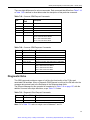
SDRAM
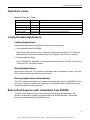
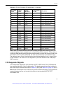
Note: The current configuration of the CPC358 has the SDRAM memory configuration set-up
parameters hard coded in the Boot Flash for a 128MB SODIMM. Do not attempt to install larger
memories. They will not be recognized.
The data port size is 64-bits. Clock drive to the module is provided from the same low-skew
clock driver that provides 66 MHz to the Master MPC8255. The clock enable signals (CKE0
and CKE1) are permanently enabled, thus the SELF-REFRESH command and operation are
unavailable. The Master MPC8255 can be programmed to provide refresh as needed. The 64bit data bus, eight data read/write mask signals, and the three command signals (WE#, CAS#,
and RAS#), and the two chip selects (S0 and S1) are provided to the module directly from the
Master MPC8255. The Master MPC8255 will automatically assert S0, then S1, during refresh
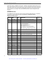
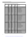
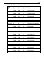
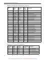
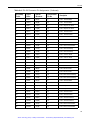
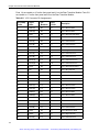
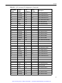
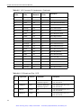
cycles. Multiplexed row/column address bits (MA0 through MA11) and bank select signals (BA0
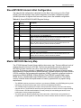
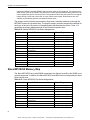
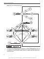
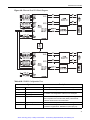
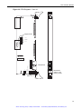
and BA1) are driven to the module from PSM549 (see Figure 4-3, “External Master SDRAM
Configuration,” on page 62). External Master SDRAM Configuration). The PSM549 PLD
creates these from the 60x bus address and bank select bits that have been latched with the
processors ALE signal and multiplexed with the processors SDAMUX signal. Burst address bits
(BADDR27 and BADDR28) are utilized directly to provide the least significant bits to the
SODIMM during column address presentation. The least significant three address lines 29-31
are unused due to the 8-byte wide data path. The SODIMM module uses BADDR27 and
BADDR28 to select one of four sequential locations as the first to be burst. Bursts occur up to a
maximum of four transfers. The remaining three locations are addressed sequentially, after a
mod 4 operation is applied to BADDR27 and BADDR28. SDA10 passes through PSM549 and
always drives MA10 on the SODIMM. During the activate command, this pin provides the row
address for A10. During a PRECHARGE command this pin selects PRECHARGE all-banks
(PSDA10 = 1), or PRECHARGE-SELECTED-BANK (PSDA10 = 0) using BANKSEL[1-2]. Four
banks are supported and BANKSEL[0] is unused. During READ and WRITE commands this
pin selects AUTO-PRECHARGE (PSDA10 = 1) or no AUTO-PRECHARGE (PSDA10 = 0).
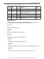
Address bit ordering conventions are opposite between the 60x bus and the SODIMM (A0 is
most significant bit) and the SODIMM (A0 is least significant bit) these are resolved within
PSM549.
External Master Support
When the Master MPC8255 is placed in 60x compatible mode, external masters can access
the SODIMM SDRAM as shown in Figure 4-3 on page 62. External masters will not multiplex
row and column addresses for the SDRAM. Therefore, an SODIMM SDRAM interface
(PSM549) has been located between the 60x address bus and SODIMM address bus. 60x
addresses are latched with ALE at the start of each memory cycle. The Master MPC8255
SDAMUX signal is used to multiplex address bits during row and column address presentation
to the SDRAM. The Master MPC8255 monitors the 60x address bus and asserts ALE,
SDAMUX, BADDR, and SDA10 appropriately for external masters.
61
Artisan Technology Group - Quality Instrumentation ... Guaranteed | (888) 88-SOURCE | www.artisantg.com