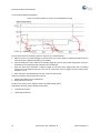
1
GPIF II Designer 1.0 Doc. No 001-75664 Rev. *B Cypress Semiconductor 198 Champion Court San Jose, CA 95134-1709 Phone (USA): 800.858.1810 Phone (Intnl): 408.943.2600 http://www.cypress.com Copyrights Copyrights © Cypress Semiconductor Corporation, 2012. The information contained herein is subject to change without notice. Cypress Semiconductor Corporation assumes no responsibility for the use of any circuitry other than circuitry embodied in a Cypress product. Nor does it convey or imply any license under patent or other rights. Cypress products are not warranted nor intended to be used for medical, life support, life saving, critical control or safety applications, unless pursuant to an express written agreement with Cypress. Furthermore, Cypress does not authorize its products for use as critical components in life-support systems where a malfunction or failure may reasonably be expected to result in significant injury to the user. The inclusion of Cypress products in life-support systems application implies that the manufacturer assumes all risk of such use and in doing so indemnifies Cypress against all charges. Trademarks ® PSoC Designer™, Programmable System-on-Chip™, PSoC Creator™, and SmartSense™ are trademarks and PSoC and CapSense® are registered trademarks of Cypress Semiconductor Corp. All other trademarks or registered trademarks referenced herein are property of the respective corporations. Source Code Any Source Code (software and/or firmware) is owned by Cypress Semiconductor Corporation (Cypress) and is protected by and subject to worldwide patent protection (United States and foreign), United States copyright laws and international treaty provisions. Cypress hereby grants to licensee a personal, non-exclusive, non-transferable license to copy, use, modify, create derivative works of, and compile the Cypress Source Code and derivative works for the sole purpose of creating custom software and or firmware in support of licensee product to be used only in conjunction with a Cypress integrated circuit as specified in the applicable agreement. Any reproduction, modification, translation, compilation, or representation of this Source Code except as specified above is prohibited without the express written permission of Cypress. Disclaimer CYPRESS MAKES NO WARRANTY OF ANY KIND, EXPRESS OR IMPLIED, WITH REGARD TO THIS MATERIAL, INCLUDING, BUT NOT LIMITED TO, THE IMPLIED WARRANTIES OF MERCHANTABILITY AND FITNESS FOR A PARTICULAR PURPOSE. Cypress reserves the right to make changes without further notice to the materials described herein. Cypress does not assume any liability arising out of the application or use of any product or circuit described herein. Cypress does not authorize its products for use as critical components in life-support systems where a malfunction or failure may reasonably be expected to result in significant injury to the user. The inclusion of Cypress’ product in a life-support systems application implies that the manufacturer assumes all risk of such use and in doing so indemnifies Cypress against all charges. Use may be limited by and subject to the applicable Cypress software license agreement. 2 Document No. 001-75664 Rev. *B GPIF II Designer 1.0 Contents GPIF II Designer 1.0 ............................................................................................................................................................... 1 Contents ................................................................................................................................................................................. 3 1. Introduction.................................................................................................................................................................... 5 1.1 1.2 1.3 1.4 2. Getting Started............................................................................................................................................................... 7 2.1 2.2 2.3 2.4 3. Welcome ............................................................................................................................................................... 5 About Help ............................................................................................................................................................. 5 Technical Support .................................................................................................................................................. 6 Document Revision History ................................................................................................................................... 6 Creating a GPIF II Project ..................................................................................................................................... 8 Designing a GPIF II Interface ................................................................................................................................ 8 Integrating GPIF II Configuration ........................................................................................................................... 9 Analyzing Signal Timings of the Interface .............................................................................................................. 9 Understanding GPIF II Designer................................................................................................................................. 11 3.1 3.2 3.3 Concepts ............................................................................................................................................................. 11 3.1.1 Cypress Supplied Interfaces ................................................................................................................... 11 3.1.2 Interface Concepts.................................................................................................................................. 12 3.1.3 FX3 DMA Architecture ............................................................................................................................ 12 3.1.4 GPIF II State Machine Concepts ............................................................................................................ 13 3.1.5 Timing Simulation Concepts ................................................................................................................... 14 User Interface ...................................................................................................................................................... 14 3.2.1 Start Page ............................................................................................................................................... 15 3.2.2 Interface Definition .................................................................................................................................. 15 3.2.3 Interface Customization .......................................................................................................................... 18 3.2.4 State Machine Canvas............................................................................................................................ 18 3.2.5 Timing ..................................................................................................................................................... 21 3.2.6 Output Window and Notice List Window ................................................................................................. 23 3.2.7 Documentation and Context Help ........................................................................................................... 23 Tabs, Menus, and Shortcuts ................................................................................................................................ 23 3.3.1 Application Toolbar ................................................................................................................................. 23 3.3.2 File Menu ................................................................................................................................................ 24 3.3.3 View Menu .............................................................................................................................................. 24 3.3.4 Build Menu .............................................................................................................................................. 25 3.3.5 Timing Simulation ................................................................................................................................... 25 GPIF II Designer 1.0 Document No. 001-75664 Rev. *B 3 Contents 3.3.6 3.3.7 4. Programming GPIF II State Machine .......................................................................................................................... 27 4.1 4.2 4.3 4.4 4.5 4.6 4.7 4 Help Menu .............................................................................................................................................. 25 Shortcut Keys ......................................................................................................................................... 26 GPIF II Overview ................................................................................................................................................. 27 GPIF II State Machine ......................................................................................................................................... 28 GPIF II Actions .................................................................................................................................................... 28 4.3.1 Action - IN_ADDR ................................................................................................................................... 33 4.3.2 Action - IN_DATA ................................................................................................................................... 33 4.3.3 Action - DR_DATA .................................................................................................................................. 34 4.3.4 Action - DR_ADDR ................................................................................................................................. 35 4.3.5 Action - COMMIT .................................................................................................................................... 35 4.3.6 Action - DR_GPIO .................................................................................................................................. 36 4.3.7 Action - LD_ADDR_COUNT ................................................................................................................... 36 4.3.8 Action - LD_DATA_COUNT .................................................................................................................... 37 4.3.9 Action - LD_CTRL_COUNT .................................................................................................................... 38 4.3.10 Action - COUNT_ADDR.......................................................................................................................... 38 4.3.11 Action - COUNT_DATA .......................................................................................................................... 38 4.3.12 Action - COUNT_CTRL .......................................................................................................................... 39 4.3.13 Action - CMP_ADDR .............................................................................................................................. 39 4.3.14 Action - CMP_DATA ............................................................................................................................... 39 4.3.15 Action - CMP_CTRL ............................................................................................................................... 40 4.3.16 Action - INTR_CPU................................................................................................................................. 40 4.3.17 Action - INTR_HOST .............................................................................................................................. 40 4.3.18 Action - DR_DRQ ................................................................................................................................... 41 GPIF II Transition Equations and Triggers .......................................................................................................... 42 GPIF II Constraints .............................................................................................................................................. 43 4.5.1 Mirror States ........................................................................................................................................... 43 4.5.2 Intermediate States................................................................................................................................. 46 Designing a GPIF II State Machine ..................................................................................................................... 47 4.6.1 Illustration of Implementing Asynchronous SRAM Interface ................................................................... 47 4.6.2 Analyzing Timing .................................................................................................................................... 55 GPIF II firmware API ............................................................................................................................................ 56 Document No. 001-75664 Rev. *B GPIF II Designer 1.0 1. Introduction 1.1 Welcome Welcome to GPIF II Designer - a software tool to configure the GPIF II port of EZ-USB® FX3 to connect to any external device. This application generates programmable register values in the form of a C header file that can be readily integrated with the firmware application code using the firmware API framework. Figure 1-1. FX3 System Overview The graphical user interface (GUI) provided by the application allows the user to define the interface in the form of a state machine diagram. The application generates warnings and error messages to guide the user on possible erroneous input. The design entered by the user is processed to generate a C program header file. GPIF II Designer also provides a set of readily usable designs of standard and popular interfaces. Detailed documentation of such interfaces describing the protocol definition along with timing diagrams are available on opening the Cypress supplied interface project using GPIF II Designer. The users can modify a few parameters of such designs to customize the design to suit to the target environment. GPIF II Designer is part of the FX3 Software Development Kit. 1.2 About Help GPIF II Designer help provides information on tool usage as well as on interfacing with the FX3 firmware. A help topic corresponding to the window on focus can be launched by pressing the function key [F1]. The help pages launched can be navigated as follows: Use the Contents tab to view all of the help topics in a structured table of contents Select Topics from the Help menu to open this help system Use the Index tab to find and view key topics alphabetically Use the Search tab to find specific topics by keywords GPIF II Designer 1.0 Document No. 001-75664 Rev. *B 5 Introduction 1.3 Technical Support If you have any technical questions or issues related to GPIF™ II Designer, you can contact Cypress by sending an email to [email protected]. More information about EZ-USB FX3 is available at www.cypress.com/go/superspeed. You can also call Cypress Customer Support, +1 (800) 541-4736 Ext. 8 (in the USA), +1 (408) 943-2600 Ext. 8 (International), Or visit www.cypress.com/go/support 1.4 Document Revision History Revision Issue Date Origin of Change Description of Change ** 01/17/2012 VTV New document. *A 02/29/2012 VTV Updated the user manual with comments from Beta customers as well as Applications and Design. The change also includes update of text and figures to reflect changes made after the beta release MRAO Updated all the figures across the document. *B 6 Document No. 001-75664 Rev. *B GPIF II Designer 1.0 2. Getting Started One of the key features of EZ-USB FX3 is the flexibility and programmability of the general programmable interface (GPIF II). GPIF II is a programmable state machine that allows a user to configure FX3 to connect to any processor interface. GPIF II state machine is defined by a set of programmable memory mapped registers. These registers are to be configured by the firmware application running on the EZ-USB FX3. The register configuration that programs GPIF II for a specific interface can be generated by the software tool GPIF II Designer. Figure 2-1. FX3 SDK Usage Flow Using GPIF II Designer The set of register values that programs the GPIF II interface is generated as a data structure supported by the FX3 firmware framework API. GPIF II Designer generates a header file that can be included in the FX3 firmware framework application code. A step-by-step procedure to use GPIF II Designer to configure FX3 is as follows: 1. Select the required Interface project from the list of Cypress Supplied Interfaces. Cypress supplied interface projects are listed on the left pane of start page. Click on the Interface to create a project. If none of the Cypress supplied interface matches the target application requirements, create a new project to design a state machine of the required interface. 2. Enter the details of the Interface to be implemented. In case of a Cypress supplied interface project, the state machine for the chosen Interface is readily available. The state machine design of a Cypress supplied interface cannot be modified. Possible customizations on the selected interface appear on the left side of the Interface Customization window. The pin diagram shown on the window provides a graphical interface to modify the pin mapping, if a change is allowed by the design. In case of a user defined interface project, the user needs to define a state machine corresponding to the interface protocol to be implemented. The state machine diagram for the interface can be drawn using the state machine canvas. The electrical interfacing details should be defined using the Interface definition tab before entering the state machine using the state machine canvas tab. 3. Once the state machine is defined for the interface, build the project to generate a GPIF II configuration header file using the “Build Project” command available below the Build menu. The header file will be generated below the project folder. Copy the header file to the firmware project folder. 4. In the firmware application, load the GPIF™ II configuration and start the state machine using the GPIF™ II configuration API. 5. The user can view the relative timing corresponding to the state machine using the Timing Simulation tab. GPIF II Designer 1.0 Document No. 001-75664 Rev. *B 7 Getting Started 2.1 Creating a GPIF II Project In order to design an Interface or use a Cypress supplied interface, the user first needs to create a GPIF II project. A new project can be created using the "New Project" command from the File menu, or by using links provided on the start page. The "New Project" command pops up the New Project dialog box as shown in the following figure. The user can enter the project name and choose the location where the project files will be stored. An existing project can be opened using File menu item "Open Project". The start page also provides links to open the most recently used projects. Figure 2-2. New Project Dialog Box A GPIF II project file is created with the name specified by the user and with the extension ".cyfx". The project will be created below a new folder named with the project name and the extension ".cydsn". Thus, if the user specifies "Async_Admux" as the project name to be created at the location "C:\MyDesigns"; a GPIF II project file "Async_Admux.cyfx" will be created below the folder "C:\MyDesigns\Async_Admux.cydsn". The New Project dialog box also provides a tab for creating a project with one of the Cypress Supplied Interfaces. Note that Cypress supplied interface implements a predefined interface and therefore cannot be edited. 2.2 Designing a GPIF II Interface Creating a new GPIF II design involves the following steps: 1. Defining the electrical interface in terms of the width of data and address buses that is used, the number and direction of control signals, and the interface clocking parameters. Defining these terms is done through the Interface Definition window. 2. Defining the behavior of the interface in terms of how the inputs are to be used and the outputs are to be driven. This description is provided in the form of a state machine that is entered through the State Machine Canvas. 8 Document No. 001-75664 Rev. *B GPIF II Designer 1.0 When a new project is created or existing project is opened, the user is greeted with the Interface Definition window, which provides a graphical display of the FX3 GPIF II port (P-Port) interface. A list of configurable parameters of the interface with selectable options appears on the left pane under Interface Settings. After completing the interface definition, a state machine diagram matching the processor interface is to be entered using the state machine canvas. States can be added from the menu that appears on the click of the right mouse button. The list of actions on the right pane can be added to a state. The GPIF II Designer users are provided with a library of standard and popular Interfaces that can be readily used. These Interfaces termed as the "Cypress supplied Interfaces" implement predefined protocols. Cypress validates the state machine corresponding to any Cypress supplied Interface to match the timing diagram and protocol definition documented along with the interface. Therefore, the user does not need to enter a state machine to generate the GPIF II header file. A few of the Interface settings, such as the pin mappings for various signals may be modified. All the modifiable settings of a Cypress supplied interface project appear on the left pane below Interface Settings. The users are provided with error and/or warning messages to guide them during design entry. The error / warning messages are displayed on the output window that can be viewed using the "Output" command from the "View" menu. After defining the electrical interface and the state machine, use the "Build Project" command to generate code that can be integrated with the FX3 firmware application. The GPIF configuration is generated as a "C" header file below the project folder. This header file is named cyfxgpif2config.h by default. This name can be modified using the "Build Settings" command on the "Build" menu. 2.3 Integrating GPIF II Configuration The generated header file contains data structures that are compliant with the EZ-USB FX3 firmware framework API. The user needs to copy the generated header file into the firmware application folder and include it in the source file. The firmware application needs to call appropriate GPIF™ II APIs to load and start the state machine. A sample code snippet that configures the GPIF™ II interface is shown as follows. /* Load the configuration into the GPIF registers. & CyFxGpifConfig is defined in the GPIF II Designer generated header file */ status = CyU3PGpifLoad (CyFxGpifConfig); if (status != CY_U3P_SUCCESS) return status; /* Start the operation of the GPIF II state machine. Both START and ALPHA_START are defined in the header file. */ status = CyU3PGpifSMStart (START, ALPHA_START); if (status != CY_U3P_SUCCESS) return status; 2.4 Analyzing Signal Timings of the Interface After entering the state machine corresponding to the P-port Interface the relative timing of the input and output signals can be simulated using the Timing Window. In order to perform timing simulation, the user needs to select a specific State Machine Path in the state machine. The selected path can be saved for further viewing in a Timing Scenario file. A saved timing scenario can be loaded from the menu provided on the top strip of the Timing Window. A new timing scenario can be created using the Create Scenario dialog box. A toolbar icon to create Scenario is provided on the top strip of the Timing Window. The user can enter a unique name to identify the scenario being created in the Scenario Name. A path consisting of a set of states that can be traversed sequentially can be selected for simulation using the Scenario Entry dialog. GPIF II Designer 1.0 Document No. 001-75664 Rev. *B 9 Getting Started Figure 2-3. Create Scenario Dialog Box A saved scenario can be loaded to display the relative timings of the input and output signals. Saved Timing Scenarios can be selected from the menu provided on the top strip. 10 Document No. 001-75664 Rev. *B GPIF II Designer 1.0 3. Understanding GPIF II Designer This section helps you to familiarize with the concepts and terms used in the GPIF II Designer User Interface and in the documentation. 3.1 Concepts This section introduces a few concepts and terms that will help you to use the tool effectively. The set of memory mapped register values that can be programmed to define the Interface settings and behavior of the GPIF II port of FX3 is termed as GPIF II configuration. A GPIF II configuration implements an interface connecting FX3 with another device connected on the GPIF II port. The term GPIF II Interface refers to the digital interface and the timing rules to be established on the GPIF II port of FX3. Apart from the type and behavior of the P-port signals, a GPIF II Interface can also define the interaction of the P-port with the data path and firmware application on the FX3 device. GPIF II Designer allows you to specify the behavior of the P-port interface of FX3 by using a state machine diagram. The state machine diagram and interface settings together define the electrical interface and behavior of the P-port. The term GPIF II design refers to the settings and state machine representation. The details of the design entered by you and the other settings regarding a user’s interaction with the tool are stored in a project file. A project file is the primary interface of a user to the tool. A project file binds all the related files corresponding to a design. The user can “Open”, “Save”, and “Save As” (copy) projects. When using the "Save As" option, a copy of the project is created under a newly created folder with the format <project name>.cydsn, i.e., a project called "Async_fifo" will be created under the folder "Async_fifo.cydsn". The project file has the extension of ".cyfx". Note The project file and the user entered designs are stored in XML files. The content and format of these files are meant to be interpreted only by the GPIF II Designer application and these are not expected to be edited otherwise. A GPIF II Interface project can be user defined or Cypress supplied. Cypress supplied interface projects implement standard protocols that are defined and tested by Cypress. User defined projects can be used to implement any custom interface and protocol desired by the user. 3.1.1 Cypress Supplied Interfaces GPIF II Designer provides a library of standard and popular Interfaces that can be readily used by FX3 SDK users. These specially parameterized and predefined Interfaces are known as Cypress supplied Interfaces. The start page provides links to open Cypress supplied interfaces. Selecting these links pops up a dialog for creating a copy of the interface project at a selectable location. Once the copy of the project is created, the user can make customizations using the Interface Customization window. The number and type of customization allowed depends on the interface selected and can include options, such as modes of operation, pin mapping for control signals, and the data bus width. Since the Cypress supplied interface projects implement a predefined and pre-verified communication protocol, the user is not allowed to make changes to the state machine that implements this protocol. The State Machine window only allows the user to view the state machine implementation provided by Cypress. A Cypress supplied interface can be converted as a normal (editable by the user) using the "Save Lib Project As Editable". The user needs to save the library project the desired location and then open the saved project. Each Cypress supplied interface project gives detailed documentation about the interface protocol in the “Documentation” tab. The documentation also gives details of the interface as well as instructions on customization GPIF II Designer 1.0 Document No. 001-75664 Rev. *B 11 Understanding GPIF II Designer and generation of the GPIF II configuration. The help section on the right side of the Customization window also provides specific help on the customizations allowed. 3.1.2 Interface Concepts Interface Definition is the process of defining the electrical interface between the FX3 device and the processor/FPGA connected to it. 3.1.2.1 Peripherals In addition to the programmable GPIF II interface, the EZ-USB FX3 device also implements a set of serial communication blocks to connect to external peripheral devices. The serial communication protocols supported are I2C (master only), I2S (master only), SPI (master only), and UART. Enabling a specific peripheral block on the FX3 has an implication on the number or pins available to be used as part of the GPIF interface. See EZ-USB FX3 Programmer's Manual for details. 3.1.2.2 Master and Slave A GPIF II interface allows the FX3 to interface with an external processor acting as a master or a slave. If the interface transactions with the external system are initiated by FX3, then FX3 is the master. FX3 is a slave if the interface transactions are initiated by the external processor (connected on the GPIF II port), and the FX3 is only expected to respond to the actions initiated by the external processor. A given GPIF II configuration used the FX3 as a master or a slave device. It is not possible to implement both modes in a single configuration. If an address bus is part of the electrical interface, this will serve as an input for slave mode designs; and as an output for master mode designs. 3.1.2.3 Interface Clocking A GPIF II based interface can be synchronous or asynchronous in nature. In the case of a synchronous project, the GPIF II state machine operates using the same clock as is used on the interface. This clock can be generated and driven out by the FX3 device, or be provided as input to the FX3 device. The maximum frequency supported for the GPIF II interface clock is 100 MHz. A given GPIF II configuration is asynchronous or synchronous. It is not possible to have both coexisting in a given configuration. 3.1.2.4 Multiplexing of Address / Data A GPIF II gives a maximum of 32 bidirectional data lines, which can be split into or time multiplexed with address lines. In the case of multiplexed operation, the address bus will have the same width as the data bus. One of the control pins can be used to implement the ADV or ALE signal required to control the functionality of address / data multiplexed bus. If the address bus is not time multiplexed with the data bus, the number of address lines available will depend on the width of the data bus. See EZ-USB FX3 datasheet for more details. 3.1.2.5 Control Signals and GPIOs A GPIF II interface is associated with: 1. 2. 3. A data bus of configurable width and direction. An optional address bus of configurable width and direction. A set of control pins of configurable direction and functionality. The number of control pins available depends on the overall I/O matrix configuration as well as on the configuration of the data and address bus. See EZ-USB FX3 Programmer's Manual for details. The available control pins can be configured as input signals that drive the GPIF II State Machine, output signals that are driven by the State Machine or flags that reflect the transfer readiness of various buffers on the FX3 device. Any pins that are unused by the GPIF II block can be configured as GPIOs that can be controlled by the firmware application. 3.1.3 FX3 DMA Architecture The FX3 device has an internal DMA fabric that connects the GPIF interface to the internal system memory. All data transfer through the GPIF interface is initially done from/into an internal memory buffer. The firmware application running on the FX3 is responsible for connecting this data path to the appropriate source or sink, such as the USB host or a serial peripheral. 12 Document No. 001-75664 Rev. *B GPIF II Designer 1.0 3.1.3.1 Sockets Each port on the USB 3.0 device supports a number of sockets that correspond to one end of a data flow and can be independently addressed. The P-port or GPIF port of the FX3 device supports a maximum of 32 sockets, which means that a total of 32 independent data transfers can be performed across this interface. The firmware application is responsible for allocating memory buffers corresponding to all sockets that need to be used; and for connecting the socket to the source of sink of data on another port. See the DMA Channel APIs in the FX3 SDK API guide for the functions that do this. 3.1.3.2 Threads Even though the GPIF port on the FX3 device provides 32 sockets that can be independently addressed and used for data transfer, there are some restrictions on how the application can switch the active socket that is used for a transfer operation. The FX3 device implements four DMA transfer handlers or threads, which are active concurrently. Each of these threads can be associated with one DMA Socket at a time. This means that the application can select a maximum of four sockets that are bound to these threads, and then switch between them with no added latency. The thread to be used for each word of data transferred can be specified directly by providing an input address, or by specifying the target thread in the IN_DATA pr DR_DATA action settings in the GPIF state machine. Changing the active socket that is bound to a thread involves additional latency. This switching can be done automatically by specifying the socket address (in cases where the address bus is between 3 and 5 bits wide) or be done with firmware intervention within the FX3 device. The GPIF hardware only provides one set of DMA status flags per thread. The thread specific DMA flags for a thread always reflect the status of the active socket on that thread. When switching the active socket on a thread, sufficient time should be provided to ensure that a flag reflects the state of the new socket before using it to control data transfers. Note that the socket to thread mapping is not flexible. Each socket ‘N’ can be bound only to the thread numbered (N MOD 4). This means that it is not possible to bind sockets 0, 4, 8, and so on, to different threads and thereby use them at the same time. The sockets to be used for GPIF data transfers should be selected keeping this constraint in mind. 3.1.3.3 Data Transfer Registers The GPIF hardware also implements a set of registers that can be used as the source or sink for data that is transferred through the GPIF data bus. These registers can be used in cases where small control messages that are used by the firmware are to be transferred. Such transfers can be selected by specifying the Data Sink or Source as Register in the IN_DATA or DR_DATA action settings. The CyU3PGpifWriteDataWords() and CyU3PGpifReadDataWords() APIs in the FX3 SDK can be used to write or read these data words from these registers from the FX3 firmware application. Even though the data transfer from/to registers is not related to the FX3 DMA fabric, four different sets of registers corresponding to the four DMA threads are provided. The GPIF action settings can be used to select the specified register set (or the thread number). The same thread number needs to be used by the firmware application when invoking the CyU3PGpifWriteDataWords() or CyU3PGpifReadDataWords() APIs. 3.1.3.4 DMA Flags Since the main purpose of any GPIF II Design is to manage data transfers into and out of the FX3 device's buffers, dealing with DMA buffer readiness and performing flow control is an essential part of these designs. The FX3 device makes use of a number of DMA buffers of programmable size to send or receive data across the GPIF II Interface, and there is a small window of time where it cannot do data transfers because the active DMA buffer is being switched. It is also possible that the DMA buffer is not ready for transfer when the external processor is trying to initiate a transfer. The FX3 device provides a set of DMA status flags that can be output on select GPIOs and used to perform flow control on the processor side. The DMA status flags can reflect one of the following: 1. 2. DMA ready status, that is, buffer empty/full indication. Data count above/below user programmable threshold indication. The FX3 firmware API needs to be used to set the threshold value for various buffers. 3.1.4 GPIF II State Machine Concepts The behavior of the GPIF II Interface in terms of how it responds to inputs and generates the outputs is described in the form of a State Machine. GPIF II Designer 1.0 Document No. 001-75664 Rev. *B 13 Understanding GPIF II Designer 3.1.4.1 GPIF II State Machine The GPIF II block is a hardware block that can implement a user specified protocol on the P-port of the EZ-USB FX3 device. The protocol to be implemented is specified in the form of a state machine, thereby allowing a wide variety of protocols to be implemented. The GPIF II State Machine also interfaces the P-port Interface to a data path on the EZ-USB FX3. Each state can be programmed to perform a set of actions. The conditions for state changes can be specified in the form of Boolean transition equations formed using the trigger variables. The trigger variables can be external signals configured as input or system generated events. 3.1.4.2 Disjoint State Machine One FX3 based system design may require multiple interfaces to be implemented on the P-port at different times. For example, the FX3 could act as a master to program an FPGA connected to it and then switch over to slave mode where it exchanges data with the FPGA. These interfaces can be implemented as different GPIF II Designer projects in which case, the GPIF block will need to be reset and reconfigured when switching modes. Another option is to implement these as disjoint or unconnected state machines within a single GPIF II designer project, so that they can be loaded into the GPIF configuration memories in a single step. These are called disjoint state machines because the GPIF hardware cannot switch from one state machine to another during normal operation. Firmware intervention is required to force any transition between different disjoint state machines. 3.1.4.3 Start State Each disjoint state machine in a GPIF II design requires a start state that cannot be associated with any actions. That start state is called dummy state, whose only purpose is to enable a transition to the actual root state of the disjoint state machine and is used by the firmware to start operation of the state machine. The GPIF II state machine is not allowed to have any transitions that end at the start state. 3.1.5 Timing Simulation Concepts The GPIF II Designer tool supports the simulation of the interface behavior based on the state machine that is programmed by the user. The user selects a path to be simulated, and the tool generates and displays a representative timing diagram of how input and output signals behave when executing the specified path. 3.1.5.1 State Machine Path A sequence of states can be seen during a traversal of the GPIF II State Machine. The path can be arbitrarily long in the case of state machines that have cycles. Each state can be repeated multiple times in a path to simulate the possibility of delays in transitioning out of that state. The timing simulation assumes that the state machine stays in each state for the minimum allowed time. 3.1.5.2 Timing Scenario A timing scenario represents the triggers and actions associated with a State Machine path of interest for the protocol implemented by the GPIF II state machine. For example, the steps involved in a single byte packet write are a specific timing scenario for the Synchronous Slave FIFO protocol. The users can specify a timing scenario in the form of the state machine path that implement this part of the protocol, and the "Timing" tab of the GPIF II Designer will display the behavior of all signals that are involved in this sequence. 3.2 User Interface The graphical framework of GPIF II Designer provides the following distinct windows: Start page Interface Definition / Customization State Machine Canvas Timing Documentation Each of the windows is accessible anywhere from the tool. All the possible operations on the tool are accessible through toolbar buttons or menu items. This section walks through the various windows and controls provided by the tool. 14 Document No. 001-75664 Rev. *B GPIF II Designer 1.0 3.2.1 Start Page The start page is the greeting page that you see when you load the GPIF II Designer application. The left pane of the start page provides links to all Cypress supplied interfaces as well as the most recently used projects. When Cypress supplied interface is selected from the start page, the user is prompted to make a copy of the project. Selecting a recently opened project reopens it. The central pane of the start page shows introductory documentation about GPIF II and the Designer tool flow. 3.2.2 Interface Definition The Interface Definition Window allows the users to define the I/O level external interface. The central pane of this window displays the graphical view of the FX3 ⇔ P-port interface. All settings related to the Interface are arranged with selectable options on the left pane. It is recommended to complete the Interface definition settings before moving to the state machine diagram. The Interface Definition Window provides following settings: 3.2.2.1 Selection of FX3 Peripherals The EZ-USB FX3 provides peripheral interfaces that can be selectively used according to the user’s application. Usage of specific peripherals may impact the availability of GPIOs for the GPIF interface. The GPIF II Designer updates its internal configuration generation logic based on this input, so that the appropriate number of GPIOs is allocated for the GPIF functionality. Note The peripheral selection is only used by the tool to calculate the available pin count. The user is responsible for setting up the FX3 I/O Matrix and peripheral blocks as required in the firmware application code. 3.2.2.2 Master / Slave Interface Selection The GPIF II Interface allows the FX3 device to connect to an external processor or FPGA as a master or a slave device. When the FX3 device is acting as a master, it initiates transactions on the interface. When the FX3 device is acting as a slave, it can only respond to transactions that are initiated by the external device. The address bus (if any) on the interface is always driven by the master and therefore is an input bus when FX3 is a slave and an output bus when FX3 is a master. A master mode design typically requires multiple disjoint state machines that implement various kinds of transactions under firmware control. A GPIF project or configuration can only contain state machines in slave mode or master mode. 3.2.2.3 Asynchronous / Synchronous Interfaces GPIF II can be programmed to implement both asynchronous and synchronous interfaces. In case of synchronous interfaces, the GPIF II clock is shared between FX3 and the external processor connected on the GPIF II port. The clock can be driven by GPIF II or can be input to GPIF II. A given GPIF II configuration is asynchronous or synchronous. Further, it is not possible to have both coexisting in a given configuration. 3.2.2.4 Address and Data Buses The data bus between FX3 and the external device can be configured as 8-bits, 16-bits, or 32-bits wide. If the data bus is not being used, it can be left configured for any of these values. The data bus is assumed to be bidirectional in all cases, though the state machine design can use only input or output actions or both as required by the communication protocol. An optional address bus can also be configured. The address bus can be time multiplexed on the same pins as the data bus and the address bus width specified is ignored in such a case. If a dedicated address bus is required, the width of the bus can be specified. The address bus is configured as input for all slave mode designs, and it is typically not useful to configure an address bus wider than 8 bits in this case. The address bus is configured as output for all master mode designs, and can be configured to have a variety of bus widths. 3.2.2.5 Signal Properties The graphical view of FX3 external interface displays the input and output signals along with the address and data buses based on the selections made by the user on the left pane. The user can double click on any signal line to bring up a dialog box to configure the signal settings. Each signal can be assigned with a user defined alphanumeric name string. The tool automatically assigns an available GPIO to each signal. This assignment of a GPIO to a signal can also be modified by double clicking on the signal. The pin (GPIO) assignment to each signal also can be modified by clicking on each the GPIO label provided along with the signal. Note that the signals that use special functions cannot be moved to other pins. GPIF II Designer 1.0 Document No. 001-75664 Rev. *B 15 Understanding GPIF II Designer 3.2.2.6 Special Function Signals Some of the general-purpose I/O signals of FX3 can be associated with special functions that are commonly used in standard protocols. These special functions are only available on specific pins and control signals that use them cannot be moved to other pins. See the FX3 datasheet for information on which GPIOs correspond to each of these functions. The special functions provided by GPIF II are as follows: 1. 2. 3. 4. 5. 6. OE: Output Enable. Provides direct control of Output Drivers. The OE signal directly controls whether the data bus is driven or tristated by the FX3, so that the latencies associated with doing this through the GPIF II State Machine are removed. WE: Write Enable. Provides direct control to disable output drivers on the data bus. The data bus will not be driven by FX3 if the WE special function is selected and the WE input is asserted. DLE: Data Latch Enable. Enables the input stage on the FX3 data bus to latch data. This special function is normally combined with the WE function. ALE: Address Latch Enable. Enables the input address stage on the FX3 to latch address values. DRQ: DMA Request. Provide a DMA request output that is controlled through the GPIF II State Machine and that responds to the DACK input signal. DACK: DMA Acknowledge. This is not a separate special function but is an input that is used to control the behavior of the DRQ signal. Special function GPIO DLE / WE GPIO_18 OE GPIO_19 ALE GPIO_27 DACK GPIO_20 DRQ GPIO_21 Note In order to assign special functionality to FX3 I/Os, the corresponding GPIO should be unused. If the GPIO is already being used, then reassign using the interactive FX3 interface diagram on Interface definition Window. 3.2.2.7 Input Signal Settings The "Input Signal Settings" dialog box allows the user to configure the selected input control signal with the following parameters. Name: User provided name for signals. This name will be displayed on the trigger list in Transition Equation Entry on the state machine canvas as well as shown on the timing simulation screen. GPIO to use: The signals can be associated with any of the available GPIOs. The tool provides a list of all unallocated GPIOs for the user to choose from. Polarity: Polarity selection is used to set the polarity of special function signals - WE, OE, DLE, ALE, and DACK. The special function is considered as asserted based on the selected polarity. For example, setting OE with active low sets Output drive functionality when this GPIO is low. The polarity setting is not used while specifying transition conditions on the state machine canvas, and the user is expected to enter the actual value of the signal that triggers a transition. 16 Document No. 001-75664 Rev. *B GPIF II Designer 1.0 Figure 3-1. Input Signal Settings Dialog Box 3.2.2.8 Output Signal Setting The "Output Signal Settings" dialog box allows the user to configure the selected output control signal with the following parameters: Name: User provided name for signals. This name is used to select the signal to be driven by the state machine, and also displayed on the timing simulation screen. GPIO to use: The signals can be associated with any of the available GPIOs. The user can choose one pin from a list of all unallocated GPIOs. Initial Value: The initial value to be driven on the I/O before the GPIF state machine starts and sets a new value. Delayed Output: Each output signal driven by the GPIF II state machine has an associated latency in terms of GPIF clock cycles. This latency is equal to 2 cycles if the delayed output checkbox is not selected, and 3 cycles if it is selected. All outputs are considered as delayed outputs by default. Polarity: The assertion from the state machine can make the signal low or high depending on this setting. Signal Mode: The signal can either be set to a specific value (asserted based on the polarity setting) or toggled from current value when driven by the state machine. In toggle mode, the value of the output signal is changed every time the signal is updated by the state machine. Figure 3-2. Output Signal Settings Dialog Box GPIF II Designer 1.0 Document No. 001-75664 Rev. *B 17 Understanding GPIF II Designer 3.2.2.9 Flag Signal Settings The "Flag Settings" dialog box allows the user to configure the selected DMA flag signal with the following parameters: Name: User provided name for signals. This name is used to select the signal to be driven by the state machine, and also displayed on the timing simulation screen. GPIO to use: The signals can be associated with any of the available GPIOs. The user can choose one pin from a list of all unallocated GPIOs. DMA flag to use: Connect the GPIO to indicate the data transfer (DMA) status such as Ready for transfer. The WaterMark flag can be used to indicate an early indication of the DMA state. The WaterMark value setting is done from the firmware API. Initial Value: The initial value to be driven on the I/O before the GPIF state machine starts and sets a new value. Polarity: The assertion from the state machine can make the signal low or high depending on this setting. Figure 3-3. Flag Settings Dialog Box 3.2.3 Interface Customization The interface customization page appears when a Cypress supplied interface project is opened. The Customization window provides three vertical panes. The left pane provides the customizable options for the opened Interface. The central pane displays the pin diagram of EZ-USB FX3 GPIF II port pins with the application processor. The user can make modifications on the pin mapping of the signals by clicking on the pins on the EZ-USB FX3 block. Quick help documentation is provided on the right pane to guide the user on customizing the parameters. 3.2.4 State Machine Canvas The state machine canvas provides graphical controls to draw a GPIF II state machine diagram. A GPIF II state machine consists of actions performed in each state and triggers that cause transition from one state to other. The "Action List" window displays the list of actions that can be added to states. The state machine canvas supports the following operations: Adding a state Single click of the right mouse button anywhere on the canvas pops-up the State Machine Menu. Select "Add State" command from the Menu to add a state to the Canvas. 18 Document No. 001-75664 Rev. *B GPIF II Designer 1.0 Adding actions to a state To add an action to a state, select the state using the left mouse button. Point to the Action to be added on the Action List Window and right click to pop-up the Action List menu. Select "Add to Selected State" command from the menu. The action list window can be brought to focus using the "Action List" command from the "view" menu. Drawing transitions between actions Bring the cursor on the state machine canvas to the center of the rectangular shape of the starting state of transition. The cursor changes shape to +. Press the left mouse button and release at the center of ending state of the transition. Adding a transition equation Bring the cursor to point to the transition line. Double click on the line to bring the "Transition Equation Entry" dialog box. All available triggers to form a transition equation are displayed as a selectable list. Select the trigger and add to the "Equation Entry" using the "Add" button. Use the necessary Boolean expression notations from the buttons on the left of the dialog box. Alternatively, the user can type the equation directly on the "Equation Entry" box to enter the Boolean expression. Click "OK" after entering the equation. Setting state properties Bring the cursor to point to the state rectangle shape. Right click to bring the State Menu. Select "Settings" from the menu to bring out the "State Settings" dialog box. Every state can be associated with a name using an alphanumeric string. Macros that map the state names to the state IDs generated by the tool are generated by the tool as part of the header generation. The "Repeat Count" property indicates the number of clock cycles to continue on the state before evaluating any outgoing transition equation. The actions associated with the state can be repeated till the transition to next state by checking the "Repeat actions until next transition". Setting action parameters Bring the cursor to point to the Action displayed on the state rectangle. Right click to open the Action menu and select "Action Settings" to bring up the "Actions Settings" dialog box. The parameters corresponding to the selected action can be configured. Click "OK" to set the configured parameters. 3.2.4.1 State Settings The state settings dialog box allows the customer to configure the properties of a state. The properties associated with a state are: Name: User provided name displayed on the state symbol on the state machine canvas. A default name is provided on creation of state and this can be edited later. This name is used to form identifier macros by prefixing the name of the project. For example, the macro "SYNC_SLAVE_FIFO_2BIT_IDLE" represents the "IDLE" state in the "SYNC_SLAVE_FIFO_2BIT" project. Repeat Count: Number of clocks cycles to continue on the state before starting to check the transition equations for exit. The default value is 0, which means that transition equations are evaluated as soon as the state is entered. Repeat Actions until next Transition: The actions specified in the state will be executed every clock cycle till transitioning to the next state. This setting is enabled by default. GPIF II Designer 1.0 Document No. 001-75664 Rev. *B 19 Understanding GPIF II Designer Figure 3-4. State Settings Dialog Box 3.2.4.2 Transition Equation Entry The "Transition Equation Entry" dialog box allows the user to enter / modify the transition equation associated with the state transition. This dialog is opened by right clicking on a transition arrow and selecting the "Settings" option. All possible triggers that can be combined to form the transition condition are displayed for selection. The Boolean expression associated with the transition can be entered using the notations and triggers provided. The entered equation appears on the list box titled "Equation Entry". The user can also enter the equation in appropriate format by directly typing into this box. Figure 3-5. Transition Equation Entry Dialog Box 20 Document No. 001-75664 Rev. *B GPIF II Designer 1.0 3.2.5 Timing GPIF II Designer converts the design entered by the user to a GPIF II Interface implementation for FX3. The state machine thus corresponds to the timing specification of a digital signal interface. The relative timing of the signals will be definite and can be represented as a timing diagram. The relative timing of the input and output signals of a state machine implementation can be simulated in the form a timing diagram using the Timing Window. Steps to perform timing simulation: 1. 2. Complete the Interface settings and state machine diagram. The project should be built without any errors. Select the state machine path to simulate timing and save it as a Timing Scenario. The toolbar icon to create Scenario is provided on the top strip of the Timing Window. The user can enter a unique name to identify the scenario. A path of the state machine can be traversed by selecting the state names appearing on the menu provided. 3. Load a timing scenario from the list. The list of saved scenarios are available for selection on the top pane of the Timing window. The input and output signal changes to implement the selected state machine path are displayed by the tool. The timings are generated on the basis of meeting minimum setup and hold time requirements and typical input/output latencies for all of the signals. The Timing window provides following features: Selection of time frame The display frame of the timing diagram can be selected by specifying the start and end of the time frame. The start and end of time frame can be specified on left and right bottom corner of the timing display respectively. Automatic Timing Scale Selection The timing window will be adjusted to the optimum scale according to the screen resolution and viewable area. Note The timing simulation is performed based on a model of the GPIF II hardware. The GPIF hardware execution is synchronous even if the interface is operating asynchronously. A typical operating (internal) clock frequency of 200 MHz (5 ns cycle time) is used in the simulation of asynchronous protocols. 3.2.5.1 Scenario Entry The state machine diagram entered can be simulated to view the relative timings and values of the signals in the form a timing diagram. The user needs to select the state machine path whose behavior is to be simulated. To select the path (state sequence) to be simulated, use the "New Scenario" command from the "Timing Simulation" menu or use the toolbar icon. The following dialog box pops up. Figure 3-6. Create Scenario Dialog Box GPIF II Designer 1.0 Document No. 001-75664 Rev. *B 21 Understanding GPIF II Designer Enter a name for the scenario being created. The name can be further used to view the timing scenario later. Select the start state of the sequence for states to be traversed. The tool then continuously provides a drop down menu showing all of the possible next states for the currently selected state, and the user can define the path by continuously selecting the desired state. The current state is available as the next state option, unless a compulsory transition is specified in the state machine. A timing scenario entered will be saved with the name specified by the user while creating. All saved timing scenarios will be available in a drop down menu on the top strip of the window. A saved scenario can be selected from this menu and modified or deleted. The Timing Simulation menu item allows one to delete or modify the scenario. Figure 3-7. Modify Scenario Dialog Box 3.2.5.2 Macro A macro is a reusable scenario corresponding to a circular timing path with repeat count. A macro is created and saved similar to creating and saving a Scenario with the exception of macro always has the same end state as the start state and has a repeat count. Typically a macro is used to analyze repeating circular state paths. Consider a burst operation. The state paths of a burst read or burst write is repeated for a number of times. Analysis of such operations can be eased by specifying it as a macro. 22 Document No. 001-75664 Rev. *B GPIF II Designer 1.0 Figure 3-8. Create Macro Dialog Box 3.2.6 Output Window and Notice List Window A combined Output and Notice List window is present at the bottom of the tool to display status and error messages. Messages indicating various operations performed on the tool, including build messages, are displayed on the Output window. The Notice List window shows error and warning messages pertaining to the design entry or selections made by the user. The user can select the Notice List or the Output window for viewing using the tabs on the bottom left. 3.2.7 Documentation and Context Help The GPIF II Designer tool includes documentation that describes tool usage and related concepts. The “Topics” item on the Help menu can be used to launch the help document. Context specific help related to each window or screen can be opened by pressing the function key [F1] after bringing the relevant window to focus. Cypress supplied interface projects also include documentation on the interface implemented by the project. This documentation includes electrical interface details and timing diagrams, as well as information of the supported customizations. Note that the datasheets presented on the tool are for providing a quick and easy guide to user. The data presented here is indicative only and must not be seen as a substitute for the full specification from which it is drawn. 3.3 Tabs, Menus, and Shortcuts The graphical framework of GPIF™ II Designer is split into the following distinct windows – Start page, Interface Definition / Customization, State Machine, Timing Simulation and Documentation. Each of the windows is accessible anywhere from the tool. Interface Customization and Documentation are applicable only for Cypress Supplied Interfaces. All the possible operations on the tool are arranged as menus accessible any time. There are following menus accessible anytime for the user namely - File, Edit, View, Build, Tools and Help. Two additional menus - State Machine and Timing Simulation appears only in the State machine tab and Timing tab respectively. The File menu provides controls to operate on the design project. Build menu provides controls to build the project and modify build related settings, and the tool menu provide modifiable options for the tool. 3.3.1 Application Toolbar A toolbar with clickable icons as shown below is provided for easier navigation between GPIF II Designer controls. GPIF II Designer 1.0 Document No. 001-75664 Rev. *B 23 Understanding GPIF II Designer The toolbar icons and their functionalities are as shown in the following table: Icon Command Description New Project Creates a new Project Open Project Opens an existing project for further modification and header file generation. Save Project Saves any modifications on the project so that the modifications are available when opened next time. Build Project Generates the header file with GPIF II Configuration. Rebuild Project Deletes the previously build header file and any other meta data associated with the project and then generates a header file. Clean Project Deletes the previously build header file and any other meta data associated with the project. 3.3.2 File Menu The File menu commands are: Menu Item Description New Project Creates a new project. User will be prompted for name and location of the project. Open Project Opens a Cypress supplied Interface project for customization and header file generation. Save Project Saves any customizations on the project so that the modifications are available when opened next time. Save Project As Copies the project to another location specified by user. User will be prompted for destination folder. Save Lib Project As Editable Available on when a Cypress supplied Interface project is opened. Converts the library project to an editable project Recent Projects Displays the list of most recently opened projects for opening Close Project Closes all project files so that the tool can open another project 3.3.3 View Menu The view menu commands bring a requested pane of the multi window application to focus. Each window pane can be closed or resized. Menu Item Description Action List Brings the Action List window pane with the selectable list of actions Output Brings the output pane on the bottom pane Notice List Brings the Notice List pane on the bottom pane 24 Document No. 001-75664 Rev. *B GPIF II Designer 1.0 3.3.4 Build Menu Build menu commands are explained as follows: Menu Item Description Build Project Generates header file on the specified folder. Default location is Project folder Clean Project Deletes the previously generated header file and related meta data Rebuild Project Generates header file using Build Project command after executing a "Clean Project" Build Settings Allows the user to change the generated header file location and name. 3.3.5 Timing Simulation The Timing Simulation menu is available only in the Timing tab. Following commands are available. Menu Item Description Create Scenario Creates a new scenario. See Scenario Entry Modify Scenario Modify a saved scenario Delete Scenario Delete a saved scenario Create Macro Create a new Macro Modify Macro Modify a saved macro Delete Macro Delete a saved macro 3.3.6 Help Menu The "Help" Menu provides essential details about the tool. See the following help commands. Menu Item Description Topics Displays a comprehensive help on the tool in a separate Window Quick Start Guide Help for the beginner About Displays version details of the software GPIF II Designer 1.0 Document No. 001-75664 Rev. *B 25 Understanding GPIF II Designer 3.3.7 Shortcut Keys Shortcut keys provide easy access to operations that is listed in the following table. Shortcut Key Function Ctrl+O Open Project Ctrl+S Save Project Ctrl+Shift+B Build Project Ctrl+Shift+C Clean Project Ctrl+Shift+R Rebuild Project F1 Show Help Tab Next Control in the window Tab+Shift Previous Control in the window Arrow Keys Move within a container control Enter Equivalent to clicking the OK button Esc Close an active dialog box 26 Document No. 001-75664 Rev. *B GPIF II Designer 1.0 4. Programming GPIF II State Machine The GPIF II Interface behavior is programmed by a user defined state machine. The state machine determines how the FX3 device responds to input signals and how it drives the output signals. The state machine also interacts with the DMA engine on the FX3 device and controls how the data is retrieved from or pushed into the DMA data buffers. Note that the FX3 firmware is responsible for setting up the DMA buffers and providing or using the data that is being transferred. This section describes the GPIF II Hardware features and how to design a GPIF II state machine. 4.1 GPIF II Overview The GPIF II port known as the P-port of FX3 provides a parallel interface with maximum of 32 bidirectional data lines. The data lines can be split into or time multiplexed into address lines. There are 13 control lines of configurable direction – configurable as IN or OUT. A programmable state machine engine controls the P-port operations and control signals. The state machine operations can be controlled by the external processor using control signals configured as input to FX3 (IN). Figure 4-1. GPIF II Subsystem The GPIF hardware also supports the generation of a set of DMA status flags indicating buffer readiness or based on a user programmed threshold, which can be used by the external processor for flow control. The use of these flags is recommended to ensure transfers without data loss. GPIF II Designer 1.0 Document No. 001-75664 Rev. *B 27 Programming GPIF II State Machine A set of counter and comparator blocks are associated with the GPIF hardware and can be used by the state machine. The comparators can check whether the current state of the address, data, or control signals match a specific pattern and generate a match signal that can be used as a trigger by the state machine. The counters can be reset or updated through state machine actions and also generate a limit match signal that can be used as a trigger. The GPIF II Designer tool generates the configuration data corresponding to the design entered by the user and this is used as an input by the APIs running in the FX3 firmware to initialize the GPIF II hardware. The EZ-USB FX3 SDK includes a set of APIs that can be used to configure, control, and monitor the GPIF interface. The GPIF hardware can trigger interrupts to the on-board ARM core on the FX3 as well as to an external processor through user specified actions selected on the state machine canvas. The GPIF II state machine can also make use of a firmware generated input signal to control the operation of the GPIF II interface. 4.2 GPIF II State Machine GPIF II is a programmable finite state machine. Every state of the state machine can be programmed to carry out instructions on the P-port and the DMA system. Such instructions known as GPIF II actions are used to create a data path between an external device connected on P-port and any other peripheral port of FX3 including the USB SuperSpeed port. Transition from one state to other is caused by Boolean expressions formed using the signals on the P-port or events generated as a result of actions. Figure 4-2. State Transition Example For example, the previous figure shows a state transition from ADDR state, which executes the GPIF II action IN_ADDR to the WRITE state, which performs the IN_DATA action. 4.3 GPIF II Actions Each state in a GPIF II state machine can be programmed to perform one or more GPIF II actions. Actions performed in a state can be programmed to be performed once or in every clock cycle till the state change occurs. 28 Document No. 001-75664 Rev. *B GPIF II Designer 1.0 The following table lists GPIF II actions. No Action Parameters Description Incompatibility with other actions 1 IN_DATA Data Sink - Register/ Socket/ PPRegister Thread Number - Thread number with which the data sink is associated. Selectable from Thread0 to 3 (This feature is available when there is no address lines to select the thread number) Sample data from data bus - This option when checked samples data from data bus but does not push in to the specified data sink. Write data into Data Sink - This option is checked when the user wants to push the sampled data in to the specified Data Sink. Samples data from data bus and moves to the destination specified. Destination can be Registers, PPRegisters or Sockets. The data in Register can be accessed using CY_U3P_PIB_GPIF_INGRESS_D ATA(thread_number) macro. The PPRegisters cannot be accessed directly from PP register space. These registers are for controlling the P-port interface in PP mode. The data in Sockets can be controlled or accessed using DMA APIs. Words from Socket can be accessed directly using firmware API CyU3PGpifReadDataWords(). Cannot be combined with DR_DATA. Cannot be combined with IN_ADDR when the address and data buses are multiplexed. 2 IN_ADDR Address Selecting - Thread or Socket Enable PP Register Access Only - This option overrides the address selection and selects PP Register space. Select a thread or socket after sampling the address word from the bus. In case of two or less address bits, the address selects one of the four threads. If the address has more than two bits, thread or socket can be selected depending upon the "Address Selecting" parameter. This parameter is available only when more than two address bits are used. "PP Register Access Only" option is made available only if the width of address bus is more than or equal to 8. Cannot be combined with IN_DATA when the address and data buses are multiplexed. 3 DR_DATA Update new value from data source This option updates the data bus with the data word present in the Source and removes the word from the specified Source. Data Source: This option facilitates the user to select between data counter and register/ Socket / PPRegister. Remove Data from the Data Source: When this option is disabled data source continue to point to same data. Drives data on to the bus from the source specified. Source can be Registers, PPRegisters or Sockets. The data in Register can sourced using be CY_U3P_PIB_GPIF_EGRESS_D ATA(thread_number) macro. The PPRegisters cannot be accessed directly from PP register space. These registers are for controlling the Pport interface in PP mode. The data in Sockets can be controlled or sourced using DMA APIs. Words from Socket can be sourced directly using firmware API CyU3PGpifWriteDataWords(). DR_DATA has two internal stages: update_bus and pop_data. The update_bus updates the data bus with the word present in the Source and happens as soon as the state machine enters the particular state. The hardware state machine works using the interface clock (in Synchronous protocols) or the FX3 internal clock (in Asynchronous protocol). Every clock cycle, the update_bus happens irrespective of "Repeat actions until next transition" option Cannot be combined with IN_DATA. Cannot be combined with DR_ADDR when the address and data buses are multiplexed. GPIF II Designer 1.0 Document No. 001-75664 Rev. *B 29 Programming GPIF II State Machine No Action Parameters Description Incompatibility with other actions in the state setting. Pop_data removes the data word from the Source and happens once or multiple times depending on the "Repeat actions until next transition" option in the state setting. 4 DR_ADDR Address Source Register / AddressCounter/ ThreadSocket Thread Number - Thread0 to 3 (Available only when number of address bits is set to 0) Update address from address source This option when checked updates the address bus with the address word present in the Address Source. But this does not remove the word from the Address Source. Remove address from address source The action removes the address word from the Address Source when this option is checked. When both of the above options are checked, update address happens first and then remove address. Drives the value from specified source to address bus. Source can be Registers, AddressCounter or ThreadSocket. The address in Register can be sourced using CY_U3P_PIB_GPIF_EGRESS_A DDRESS(thread_number) macro. The data in Sockets can be controlled or sourced using DMA APIs. Words from Socket can be sourced directly using firmware API CyU3PGpifWriteDataWords(). can use an The user AddressCounter to source the address. Cannot be combined with DR_DATA when the address and data buses are multiplexed. 5 COMMIT Thread Number - Thread0 to 3 (Available only when number of address bits is set to 0) Commit or wraps up the buffer associated to the selected Ingress thread and socket. The buffer will be transferred to the consumer side of the pipe. Typically this is used to wrap up the buffer in between a transaction prematurely. None 6 DR_GPIO Signal name - The External GPIO name Delayed output - This option introduces delay of one clock cycle before driving the GPIO. Signal mode - Toggle or Assert Output Type: In synchronous mode signal is driven after 2 clock cycles when early mode is selected and 3 clock cycles when Delayed mode is selected. In asynchronous mode the latency is 25 ns for early mode and 30 ns for Delayed mode Drives the GPIO signal to HIGH / LOW or toggles the value immediately or after a delay of one clock cycle. There will be output latency observed by the interface between the time DR_GPIO action being called and the change in GPIO signal in the interface. "Repeat actions until next transition" in the state setting has no effect on the behavior of the DR_GPIO action. This action is repeated for every clock cycle. (Clock being the interface clock or the FX3 internal clock). None 7 LD_ADDR_C OUNT Counter type - Up or Down Counter load value - The initial value of the counter. Counter limit value - The limit of counter Counter step value - The step resolution Reload counter on reaching limit - When checked, the counter resets itself upon reaching the limit. Counter mask event - This option when checked, prevents the internal event from interrupting the FX3 CPU. This action loads the counter with initial settings. Initial settings are loaded while starting the state machine. This value need to be same in all states within a given state machine diagram. Multiple values are not allowed. These settings can be overridden using firmware APIs. The counter upon reaching the limit, the hardware sets the ADDR_CNT_HIT internal trigger signal. This action is generally used with Cannot be combined with COUNT_ADDR 30 Document No. 001-75664 Rev. *B GPIF II Designer 1.0 No Action Parameters Description Incompatibility with other actions COUNT_ADDR, and ADDR_CNT_HIT trigger. The count value can also be programmed by firmware application using CyU3PGpifInitAddrCounter(). The value programmed to the register at the time of execution of state machine will be used. 8 LD_DATA_C OUNT Counter type - Up or Down Counter load value - The initial value of the counter. Counter limit value - The limit of counter Counter step value - The step resolution Reload counter on reaching limit - When checked, the counter resets itself upon reaching the limit. Counter mask event - This option when checked, prevents the internal event from interrupting the FX3 CPU. This action loads the counter with initial settings. Initial settings are loaded while starting the state machine. This value need to be same in all states within a given state machine diagram. Multiple values are not allowed. These settings can be overridden using firmware APIs. The counter upon reaching the limit, the hardware sets the DATA_CNT_HIT internal trigger signal. This action is generally used with COUNT_DATA, and DATA_CNT_HIT trigger. The count value can also be programmed by firmware application using CyU3PGpifInitDataCounter(). The value programmed to the register at the time of execution of state machine will be used. Cannot be combined with COUNT_DATA 9 LD_CTRL_C OUNT Counter type - Up or Down Counter load value - The initial value of the counter. Counter limit value - The limit of counter Counter step value - The value is always fixed to 1. Reload counter on reaching limit - When checked, the counter resets itself upon reaching the limit. Counter mask event - This option when checked, prevents the internal event from interrupting the FX3 CPU. This action loads the counter with initial settings. Initial settings are loaded while starting the state machine. This value need to be same in all states within a given state machine diagram. Multiple values are not allowed. These settings can be overridden using firmware APIs. The counter upon reaching the limit, the hardware sets the CTRL_CNT_HIT internal trigger signal. This action is generally used with COUNT_CTRL, and CTRL_CNT_HIT trigger. The count value can also be programmed by firmware application using CyU3PGpifInitCtrlCounter(). The value programmed to the register at the time of execution of state machine will be used. Cannot be combined with COUNT_CTRL 10 COUNT_AD DR None Increments/ decrements the address counter value each time the state is visited. The hardware produces ADDR_CNT_HIT event upon reaching the limit value specified during LD_ADDR_COUNT. Cannot be combined with LD_ADDR_COUNT 11 COUNT_DA TA None Increments/ decrements the data counter value each time the state is visited. The hardware produces DATA_CNT_HIT event upon reaching the limit value specified Cannot be combined with LD_DATA_COUNT GPIF II Designer 1.0 Document No. 001-75664 Rev. *B 31 Programming GPIF II State Machine No Action Parameters Description Incompatibility with other actions during LD_DATA_COUNT. 12 COUNT_CT RL None Increments/ decrements the control counter value each time the state is visited. The hardware produces CTRL_CNT_HIT event upon reaching the limit value specified during LD_CTRL_COUNT. Cannot be combined with LD_CTRL_COUNT 13 CMP_ADDR Comparator mode - Value match or Change detection Comparator value - Value against which the address being compared. Unmask value - The value specified here is ANDed with the sampled address word and then the result is used for comparison. Comparator mask event - This option when checked, prevents the internal event from interrupting the FX3 CPU. Compares sampled address with specified comparison value or detects any change in the address value. "Repeat actions until next transition" in the state setting has no effect on the behavior of the CMP_ADDR action. This action is repeated for every clock cycle. (Clock being the interface clock or the FX3 internal clock). Cannot be combined with IN_DATA when the address and data buses are multiplexed. 14 CMP_DATA Comparator mode - Value match or Change detection Comparator value - Value against which the data being compared. Unmask value - The value specified here is ANDed with the sampled data word and then the result is used for comparison. Comparator mask event - This option when checked, prevents the internal event from interrupting the FX3 CPU. Compares sampled address with specified comparison value or detects any change in the data value. "Repeat actions until next transition" in the state setting has no effect on the behavior of the CMP_DATA action. This action is repeated for every clock cycle. (Clock being the interface clock or the FX3 internal clock). Cannot be combined with DR_DATA. Cannot be combined with IN_ADDR when the address and data buses are multiplexed. 15 CMP_CTRL Comparator mode - Value match or Change detection Comparator value - Value against which the data being compared. Unmask value - The value specified here is ANDed with the sampled data word and then the result is used for comparison. Comparator mask event - This option when checked, prevents the internal event from interrupting the FX3 CPU. Compares sampled control word with specified comparison value or detects any change in the control value. "Repeat actions until next transition" in the state setting has no effect on the behavior of the CMP_CTRL action. This action is repeated for every clock cycle. (Clock being the interface clock or the FX3 internal clock). None 16 INTR_CPU None Generates CYU3P_GPIF_EVT_SM_INTERR UPT event to the FX3 CPU which can be serviced by the registered interrupt callback in the firmware. None 17 INTR_HOST None Drives the INTR pin in the Pport interface to indicate the presence of interrupt signal to the external processor. The INTR pin should be connected to the external processor. None 18 DR_DRQ Assert DRQ on – The DRQ signal can be asserted using any of the options. 1) From DMA engine 2) On assertion from the external processor on the DACK pin of FX3 3) On deassertion of DACK from the Drives the DRQ pin in the Pport interface to indicate the presence of data request to the external processor. The signal should be connected to external processor on which the DRQ is enabled. None 32 Document No. 001-75664 Rev. *B GPIF II Designer 1.0 No Action Parameters Description Incompatibility with other actions external processor on the DACK pin of FX3 4) From state Machine using the DR_DRQ action Deassert DRQ on - The DRQ is deasserted using any of the options 1) On assertion from the external processor on DACK pin of FX3 2) On deassertion from the external processor on DACK pin of FX3 3) From state Machine using the DR_DRQ action. 4.3.1 Action - IN_ADDR The IN_ADDR action causes the GPIF hardware to sample the value from the address bus and use it to select a DMA thread or a socket. See the FX3 datasheet and SDK API documentation for more details on DMA threads and sockets. When the address bus width is less than or equal to two bits, the address can only select a DMA thread. If the address is between three and five bits wide, it can select either a DMA thread or a specific socket. The “Address Selecting” parameter shown in the dialog above is used to make this selection. Figure 4-3. IN_ADDR Action Settings Dialog Box The following parameter is associated with this action: Address Selecting - Thread or Socket 4.3.2 Action - IN_DATA The IN_DATA action samples data from data bus and moves to the destination specified. Destination can be DMA channel or the firmware application. See firmware API CyU3PGpifReadDataWords(). Note that the option for selecting destination thread is available only when the destination is DMA channel with addressing mode as Thread selected by State machine (Number of address lines =0). It is possible to only latch the data from the data bus and not store it in the selected destination, or to store previously latched data into the selected destination. These options are made available to satisfy certain protocols where the data on the bus may lead a strobe signal that indicates data availability. GPIF II Designer 1.0 Document No. 001-75664 Rev. *B 33 Programming GPIF II State Machine Figure 4-4. IN_DATA Action Settings Dialog Box The following parameters are associated with this action: Data Sink - Register/ Socket/ PPRegister Thread Number - Thread number with which the data sink is associated. Selectable from Thread0 to 3 (This feature is available when there is no address line to select the thread number or master mode is enabled) Sample data from data bus - This option when checked samples data from data bus but does not push in to the specified data sink. Write data into Data Sink - This option is checked when the user wants to push the sampled data in to the specified Data Sink. 4.3.3 Action - DR_DATA The DR_DATA action drives data on bus from the source specified. The source can be DMA channel or the firmware application. See firmware API CyU3PGpifWriteDataWords(). Note that the option for selecting source as thread number is available only when the source is DMA channel with addressing mode as Thread selected by State machine (Number of address lines =0). Figure 4-5. DR_DATA Action Settings Dialog Box The following parameters are associated with this action: Update new value from data source - This option updates the data bus with the data word present in the Source and removes the word from the specified Source. Data Source - This option facilitates the user to select between data counter and register/ Socket / PPRegister. Thread Number - Thread number with which the data source is associated. Selectable from Thread0 to 3 (This feature is available when there is no address line to select the thread number) 34 Document No. 001-75664 Rev. *B GPIF II Designer 1.0 Remove Data from the Data Source: When this option is disabled data source continue to point to same data. Note "Update new value from data source" flag overrides the "Repeat actions until next transition" flag on the State Settings dialog box. This means if "Update new value from data source" checkbox is selected data will be updated on the bus in every clock cycle when FX3 is in that state even if the "Repeat actions until next transition" flag is unchecked. 4.3.4 Action - DR_ADDR The DR_ADDR action drives the value from specified the source to address bus. The source can be DMA channel or the firmware application. Figure 4-6. DR_ADDR Action Settings Dialog Box The following parameters are associated with this action: Address Source - Register / AddressCounter/ ThreadSocket Thread Number - Thread0 to 3 (Available only when number of address bits is set to 0) 4.3.5 Action - COMMIT Commit the data packet / buffer on the selected Ingress DMA channel. The buffer will be transferred to the other side of the pipe. This action is typically used to force buffer / packet end using state machine. Figure 4-7. COMMIT Action Settings Dialog Box The following parameters are associated with this action: Thread Number - Thread0 to 3 (Available only when number of address bits is configured 0 or master mode is enabled). GPIF II Designer 1.0 Document No. 001-75664 Rev. *B 35 Programming GPIF II State Machine 4.3.6 Action - DR_GPIO The DR_GPIO action drives the GPIO signal to HIGH / LOW or toggles value after “Assertion Delay” cycles. In case of synchronous mode the delay can be selected between two and three cycles, and in case of asynchronous system the delay can be 25 ns or 30 ns. The GPIO driven using the action will be deasserted during transition to next state. Figure 4-8. DR_GPIO Action Settings Dialog Box The following parameters are associated with this action: Signal name: User defined alphanumeric string to indicate the signal can be entered here. This name will appear on the state machine canvas. Delayed output: This parameter controls the delay of the output signal being driven. The delay will be 25 ns in asynchronous mode or 2 clock cycles in synchronous mode when the parameter box is unchecked. The delay will be 30 ns in asynchronous mode or 3 clock cycles in synchronous mode when the parameter box is checked. Signal mode: In Toggle mode the signal value gets toggled; In Assert mode the signal value will be driven as per the Polarity of the signal. Polarity of the signal is configured from Interface Definition Window. Note 1. The delayed output and signal mode settings are global for each signal and cannot be changed every time the action is used in a different state. The tool will generate a configuration file that corresponds to the last settings that were made for each output signal. 2. "Repeat actions until next transition" in the state setting has no effect on the behavior of the DR_GPIO action. This action is repeated for every clock cycle. (Clock being the interface clock or the FX3 internal clock). 4.3.7 Action - LD_ADDR_COUNT This action loads the counter settings. Settings are loaded while starting the state machine. This value will be same for a given state machine diagram. 36 Document No. 001-75664 Rev. *B GPIF II Designer 1.0 Figure 4-9. LD_ADDR_COUNT Action Settings Dialog Box The following parameters are associated with this action: Counter type (Up / Down): Counter can be configured to count in ascending / descending order. Counter load value: Initial count loaded when this action is performed. Counter limit value: The count value at which the event should be generated. Reload on reaching limit reached: The count load value can be reloaded when the count limit value is hit by checking this parameter box. Counter mask event: If the box is unchecked, firmware event is generated when the counter limit is reached. Counter step value: Counter step value that should be added/subtracted each time the COUNT_ADDR action is used. 4.3.8 Action - LD_DATA_COUNT This action loads the counter with initial settings. Initial settings are loaded while starting the state machine. This value need to be same in all states within a given state machine diagram. Multiple values are not allowed. Figure 4-10. LD_DATA_COUNT Action Settings Dialog Box The following parameters are associated with this action: Counter type (Up / Down): Counter can be configured to count in ascending / descending order. GPIF II Designer 1.0 Document No. 001-75664 Rev. *B 37 Programming GPIF II State Machine Counter load value: Initial count loaded when this action is performed. Counter limit value: The count value at which the event should be generated. Reload on reaching limit reached: The count load value can be reloaded when the count limit value is hit by checking this parameter box. Counter mask event: If the box is unchecked, firmware event is generated when the counter limit is reached. Counter step value: Counter step value that should be added / subtracted each time the COUNT_DATA action is used. 4.3.9 Action - LD_CTRL_COUNT This action loads the counter with initial settings. Initial settings are loaded while starting the state machine. This value need to be same in all states within a given state machine diagram. Multiple values are not allowed. Figure 4-11. LD_CTRL_COUNT Action Settings Dialog Box The following parameters are associated with this action: Counter type (Up / Down): Counter can be configured to count in ascending / descending order. Counter load value: Initial count loaded when this action is performed. Counter limit value: The count value at which the event should be generated. Reload on reaching limit reached: The count load value can be reloaded when the count limit value is hit by checking this parameter box. Counter mask event: If the box is unchecked, firmware event is generated when the counter limit is reached. Counter step value: Counter step value that should be added / subtracted each time the COUNT_CTRL action is used. 4.3.10 Action - COUNT_ADDR Update Address counter value by the step value configured through the LD_ADDR_COUNT action. The ADDR_CNT_HIT trigger will become true if this update results in the count reaching the specified limit. Note that there are no parameters associated with this action. 4.3.11 Action - COUNT_DATA Update Data counter value by the step value configured through the LD_DATA_COUNT action. The DATA_CNT_HIT trigger will become true if this update results in the count reaching the specified limit. 38 Document No. 001-75664 Rev. *B GPIF II Designer 1.0 Note that there are no parameters associated with this action. 4.3.12 Action - COUNT_CTRL Update Control counter value by the step value configured through the LD_CTRL_COUNT action. The CTRL_CNT_HIT trigger will become true if this update results in the count reaching the specified limit. Note that there are no parameters associated with this action. 4.3.13 Action - CMP_ADDR Compares address sampled with specified comparison value. Figure 4-12. CMP_ADDR Action Settings Dialog Box The following parameters are associated with this action: Comparator mode: In value match mode, compares the current address value with the comparator value. In Change detection mode, any change in the address value will cause a comparator match. Unmask value: Use this value to unmask the bits to be compared. Comparison value: Value to compare the address against. Comparator mask event: When you uncheck this parameter, it will cause an event to be generated to the firmware application on comparator match. Note "Repeat actions until next transition" in the state setting has no effect on the behavior of the CMP_ADDR action. This action is repeated for every clock cycle. (Clock being the interface clock or the FX3 internal clock). 4.3.14 Action - CMP_DATA Compares data sampled with specified comparison value Figure 4-13. CMP_DATA Action Settings Dialog Box GPIF II Designer 1.0 Document No. 001-75664 Rev. *B 39 Programming GPIF II State Machine The following parameters are associated with this action: Comparator mode: In value match mode, compares the current data value with the comparator value. In Change detection mode, any change in the data value will cause a comparator match. Unmask value: Use this value to unmask the bits to be compared. Comparison value: Value to compare the data against. Comparator mask event: When you uncheck this parameter, it will cause an event to be generated to the firmware application on comparator match. Note "Repeat actions until next transition" in the state setting has no effect on the behavior of the CMP_DATA action. This action is repeated for every clock cycle. (Clock being the interface clock or the FX3 internal clock). 4.3.15 Action - CMP_CTRL Compares control bits with specified comparison value Figure 4-14. CMP_CTRL Action Settings Dialog Box The following parameters are associated with this action: Comparator mode: In value match mode, compares the current control signal values with the comparator value. In Change detection mode, any change in the unmasked control signals will cause a comparator match. Unmask value: Use this value to unmask the bits to be compared. Comparison value: Value to compare the control signals against. Comparator mask event: When you uncheck this parameter, it will cause an event to be generated to the firmware application on comparator match. Note "Repeat actions until next transition" in the state setting has no effect on the behavior of the CMP_CTRL action. This action is repeated for every clock cycle. (Clock being the interface clock or the FX3 internal clock). 4.3.16 Action - INTR_CPU Interrupts the on-chip CPU to generate CYU3P_GPIF_EVT_SM_INTERRUPT event, which is to be handled by the firmware application. Note that there are no parameters associated with this action. 4.3.17 Action - INTR_HOST Interrupt the external processor by driving the INTR pin on P-Port. The INTR pin should be connected to external processor. Note that there are no parameters associated with this action. 40 Document No. 001-75664 Rev. *B GPIF II Designer 1.0 4.3.18 Action - DR_DRQ This action drives the DRQ pin in the P-port interface to indicate the presence of data request to the external processor. The signal should be connected to external processor on which the DRQ is enabled. Figure 4-15. DR_DRQ Action Settings Dialog Box The following parameters are associated with this action: DRQ value - Asserted or Deasserted Assert DRQ on – The DRQ signal can be asserted using any of the options. From DMA engine On assertion from the external processor on the DACK pin of FX3 On deassertion of DACK from the external processor on the DACK pin of FX3 From state Machine using the DR_DRQ action Deassert DRQ on - The DRQ is deasserted using any of the options On assertion from the external processor on DACK pin of FX3 On deassertion from the external processor on DACK pin of FX3 From state Machine using the DR_DRQ action GPIF II Designer 1.0 Document No. 001-75664 Rev. *B 41 Programming GPIF II State Machine 4.4 GPIF II Transition Equations and Triggers The triggers causing state transitions in a GPIF II state machine are Boolean expressions formed using trigger variables. The state transition equations can be formed using P-port signals or events generated as a result of P-port actions. The following table captures events generated as a result of the GPIF II actions. No Event Action Causing the Description Event 1 Input signal name None; This is an external event Name associated with any GPIO configured as input can be used as trigger in a transition equation. 2 FW_TRG Firmware application This trigger can be generated from the firmware using the firmware API CyU3PGpifControlSWInput() 3 INTR_PENDING Interrupt to CPU This is true only when the CPU/Host yet to read the previous raised Interrupt 4 CTRL_CNT_HIT COUNT_CTRL This trigger is true when the count specified Is reached. This trigger is generated as a result of COUNT_CTRL action 5 ADDR_CNT_HIT COUNT_ADDR This trigger is true when the count specified Is reached. This trigger is generated as a result of COUNT_ADDR action 7 DATA_CNT_HIT COUNT_DATA This trigger is true when the count specified Is reached. This trigger is generated as a result of COUNT_DATA action 8 CTRL_CMP_MATCH CMP_CTRL This trigger is true when the control pattern and mask matches with the current GPIO. This trigger is generated only with the CMP_CTRL action is specified in parent state. 9 DATA_CMP_MATCH CMP_DATA This trigger is true when the data pattern and mask matches with the current data. This trigger is generated only with the CMP_DATA action is specified in parent state. 10 ADDR_CMP_MATCH CMP_ADDR This trigger is true when the address pattern and mask matches with the current address read. This trigger is generated only with the CMP_ADDR action is specified in parent state. 11 DMA_RDY_CT,DMA_RDY_TH0,D MA_RDY_TH1,DMA_RDY_TH2,D MA_RDY_TH3 IN_DATA DR_DATA This trigger is true when the DMA is ready to send or receive data. 12 DMA_WM_CT,DMA_WM_TH0,DM A_WM_TH1,DMA_WM_TH2,DMA_ IN_DATA WM_TH3 This is true when the active DMA thread crosses the transferred data above the watermark. 13 DMA_RDY_ADDR This trigger is true when the DMA is ready to send or receive address 14 IN_REG_CR_VALID,IN_REG0_VA LID, IN_REG1_VALID, IN_DATA IN_REG2_VALID, IN_REG3_VALID This trigger is true when the data in the Input register (INGRESS_DATA_REGISTER) is valid. 15 OUT_REG_CT_VALID,OUT_REG0 _VALID, OUT_REG1_VALID, DATA_DR OUT_REG2_VALID, OUT_REG3_VALID This trigger is true when the data in the output register (EGRESS_DATA_REGISTER) is valid. 42 DR_ADDR Document No. 001-75664 Rev. *B GPIF II Designer 1.0 4.5 GPIF II Constraints The GPIF II hardware imposes some limitations on the state machines that can be implemented. Mainly, these limitations are: Full support is limited to state machines that are limited to two (or fewer) outgoing transitions from each state. Such state machines are called binary state machine in the rest of this document. Each transition equation is limited to the use of four (or fewer) trigger variables. These limitations can be surmounted by making certain changes to the state machine design. The two main techniques that can be used are: 1. 2. Using mirror states Using intermediate dummy states The GPIF II Designer tool applies the first technique automatically on state machines that do not satisfy the constraints. However, it is possible that the tool is unable to identify a set of transformations that allow the state machine to be mapped to the GPIF hardware. In such a case, the tool outputs the error message "Unable to synthesize state machine". The user can follow the state machine entry guidelines to try and resolve these errors. If the error persists despite making these changes, contact Cypress support for assistance. 4.5.1 Mirror States The mirror state machine technique makes use of a GPIF II feature that is introduced to facilitate state machine designs that violate the previously described rules. The GPIF II hardware supports working with multiple copies of a binary state machine, where the active state machine copy is determined using the current value of a trigger variable. For example, consider the state machine fragment shown as follows. This state machine has a state S0, which has four outgoing transitions based on the transition equations !ABC, !AD, ABC, and AD. Figure 4-16. A GPIF II State Machine Example Requiring Mirror States The term A can be removed from these transition equations to obtain the two modified state machines shown in the following figure. GPIF II Designer 1.0 Document No. 001-75664 Rev. *B 43 Programming GPIF II State Machine Figure 4-17. A GPIF II State Machine Split as Mirror States In this case, S0’ is inserted as a mirror state of S0. S0 has valid transitions pointing to S1 and S2 and S0’ has valid transitions pointing to S3 and S4. The state machine {S0, S1, S2} is applicable when the trigger variable A has a value of 0 and the state machine {S0’, S3, S4} is applicable when the trigger variable A has a value of 1. The GPIF hardware automatically selects the correct state from between S1 and S3 or from between S2 and S4, by looking at the current value of A. This GPIF II Designer tries to apply this feature to implement state machines that have too many out transitions from a state as well as state machines that use transition equations with many triggers. The derived state machines using this procedure need to follow a set of GPIF II mirroring rules, in order to become implementable without side effects. A real example of this method is provided in the mirror states example section. 4.5.1.1 Mirror State Rules The GPIF hardware allows up to 8 mirror state machines to be created, so that the active mirror is selected based on the current value of up to three input signals. The input signals that are used to select the active mirror state machine are called Global Triggers. There are a set of rules that need to be satisfied by all the mirror state machines. The GPIF II Designer tries to identify a set of global triggers that reduce the state machine to one that satisfies the following rules. The transitions can be split into groups of two each, such that each group applies to a specific combination of trigger values. The transitions in each group should have the same transition equations after the global trigger terms have been removed. The target states that share the same transition equation should not use conflicting actions. See the table listing GPIF II Actions for details on incompatible actions. The tool first attempts to find a solution with one global trigger, then with two, and finally with three global triggers. If the tool is unable to find a state machine reduction that satisfies the above conditions with any of these levels, it will come back with an error message saying that the state machine input cannot be synthesized. In many cases, such state machine mapping errors are a consequence of incompletely specified input. See the guidelines section for some ideas on how the state machine definition can be improved to aid the tool in finding a solution. 4.5.1.2 Mirror States Example The following figure shows a part of the Synchronous Slave FIFO protocol implementation that is included with GPIF II Designer as a Cypress supplied interface project. 44 Document No. 001-75664 Rev. *B GPIF II Designer 1.0 Figure 4-18. Slave FIFO Interface Example State Machine Requiring Mirror States The IDLE state is where the state machine waits for control signals to start performing a data transfer. Depending on the input signals, it may transition to one of four states: 1. 2. 3. RD state where a read operation is handled. Transition to the RD state is triggered by the RD input signal getting asserted while the WR and the END input signals stay deasserted. The IN_ADDR and DR_DATA actions are associated with the RD state. WR state where a general write operation (not end of packet) is handled. Transition to the WR state is triggered by the WR input getting asserted while the RD and END signals are deasserted. The IN_DATA action is associated with this state. SLP state where a single word write operation is handled (data along with end of packet signaling). Transition to the SLP state is triggered by the WR and END inputs being triggered while RD stays deasserted. The IN_DATA and COMMIT actions are associated with this state. 4. ZLP state where a zero length write operation is handled (no data, only end of packet signaling). This transition is triggered by END being asserted while RD and WR are both deasserted. The COMMIT action is associated with this state. The GPIF II Designer tool converts the above state machine fragment into the following implementation that has four mirror state machines. The conditions under which each of the four mirrors is active are listed on top. You can see that all of the transitions that are shown going to the right, share the same transition equation and the actions specified in these states are non-conflicting. Figure 4-19. Slave FIFO Interface Example Implementation with Mirror States GPIF II Designer 1.0 Document No. 001-75664 Rev. *B 45 Programming GPIF II State Machine 4.5.1.3 Guidelines for Transition Equation Entry In many cases, the GPIF II designer is unable to reduce the input state machines to an implementable form because of insufficient input information. For example, consider another form of the state machine fragment shown in the Mirror state example. This version of the state machine cannot be converted into multiple mirrored state machines that satisfy the mirroring rules using any global trigger combination. Figure 4-20. State Machine Example with Mirror States The problem is that the transition equations are not well defined. For example, the tool needs to assume that the IDLE → RD transition can happen independent of the values of the WR and END signals. If all of the transition equations are made well defined by adding expected values for the other input signals, the state machine gets transformed into the version shown in the example and the tool is able to reduce the state machine to an implementable form. In general, specifying each transition equation (particularly for the transitions originating from a state that has more than two output transitions) fully by listing the expected value of all trigger inputs will help the tool find a mapping of the state machine to the GPIF hardware. In the absence of such data, the tool treats the unspecified triggers as don’t cares for a particular transition, and may fail to find an implementable mapping. It is also recommended to avoid transition equations that involve multiple OR clauses in states that have more than two output transitions. This is because transition equations that have OR clauses typically cannot be refactored to remove global triggers. 4.5.2 Intermediate States Intermediate states can be inserted into the state machine to reduce the number of state transitions originating at a state. Consider the state machine fragment shown in the following figure. There are four transitions originating at state S0, with the transition equations F1, F2, F3, and F4 respectively. Figure 4-21. Example State Machine with Multiple Transitions 46 Document No. 001-75664 Rev. *B GPIF II Designer 1.0 The above state machine can be transformed into the version shown below. Here Sx and Sy are dummy states that have been inserted to meet the constraint that each state can have only two outgoing transitions. Figure 4-22. GPIF II Implementation for Multiple Transitions Avoiding Mirror States This kind of transformation has an impact on the overall latency between states. For example, the actions specified in the state S1 will now be performed with an additional delay of 1 cycle. Similarly, the input values that trigger the S0 → S1 transition now need to stay valid for one additional cycle. Since these system-level timing changes cannot be assumed safely, such transformations are not automatically performed by the GPIF II Designer tool. This technique can be used as applicable by the user to reduce state machines to an implementable form. 4.6 Designing a GPIF II State Machine This section illustrates how to design a GPIF II state machine to implement a GPIF II port interface using the GPIF II Designer application. The user starts with a clear definition of the interface to be implemented on the GPIF II port along with a clear view of how the interface interacts with the FX3 firmware application. The definition of the interface is typically specified using a timing diagram. The timing diagram and the protocol definition should specify the relative timing requirements between input and output signals and bus activities. The details of GPIF II design that needs to be entered into the tool are conveniently categorized as two parts: The physical layout of the interface and related details including clock settings. The behavior of the interface in terms of how a signal or bus activity or a DMA operation is to be timed. This is specified a state machine diagram. This is best explained using a real interface example as done in the subsequent sections. 4.6.1 Illustration of Implementing Asynchronous SRAM Interface Let us consider the implementation of a standard slave implementation of asynchronous SRAM interface. The asynchronous SRAM interface uses the industry-standard SRAM control bus with Chip Enable, Read (Output) Enable, and Write Enable (CE#, OE#, WE#). READ operations are initiated by bringing CE# and OE# LOW while keeping WE# HIGH. Valid data will be driven out of the data bus after the specified access time has elapsed. WRITE operations occur when CE# and WE# are driven LOW. The data to be written is latched on the rising edge of CE# or WE# (whichever occurs first). The timing diagrams are shown as follows. GPIF II Designer 1.0 Document No. 001-75664 Rev. *B 47 Programming GPIF II State Machine Figure 4-23. Asynchronous SRAM Read Timing Diagrams 48 Document No. 001-75664 Rev. *B GPIF II Designer 1.0 GPIF II Designer 1.0 Document No. 001-75664 Rev. *B 49 Programming GPIF II State Machine Subsequent sections illustrate how the above timing diagrams can be entered to GPIF II Designer to implement this interface on FX3. 4.6.1.1 Defining the Interface In order to design an interface using GPIF II Designer, start creating a GPIF II Design project. A new project can be created using the "New Project" command from the File menu, or by using links provided on the start page. The "New Project" command pops up the New Project dialog box as shown below. The user can enter the project name and choose the location where the project files will be stored. See section Creating a GPIF II Project for a detailed description. An existing project can be opened by using File menu item "Open Project". The start page also provides links to open the most recently used projects. Once a project is opened, the user is greeted with the Interface Definition window where the user is allowed to enter the electrical interface details. See Interface Definition for details on the Interface definition window. Selections applicable for Asynchronous SRAM interface are: Interface Type - Slave Communication Type - Asynchronous Data bus width - Chose 8, 16, or 32 as the case may be. Address/data bus multiplexed - Unchecked (Non multiplexed) Number of address pins used - User can enter a value from 1 to 8 depending on the target application. There are three input signals. Input signals WE and OE are assigned special functionalities of Write Enable and Output Enable. Also the internal data latch can be used by selecting the DLE (data Latch Enable). See Interface Definition for details of special functions. A screenshot of Interface definition with the above settings is shown below for reference. Figure 4-24. Interface Definition for Asynchronous SRAM 50 Document No. 001-75664 Rev. *B GPIF II Designer 1.0 FX3 Peripherals used The FX3 I/O lines are shared with other peripheral interfaces supported by FX3 that includes GPIF II. The selection of peripherals being used enables the tool can calculate the I/O lines available. Ensure the checkbox corresponding to the unused peripheral is unchecked. Clock Settings If the GPIF II port transactions are synchronized using clock, “Communication type” should be set to synchronous mode. If Synchronous mode is selected user is provided to make selections on “Clock Settings”. For this design Communication type is selected as asynchronous. Endianness The “Endianness” feature enables the FX3 device to comprehend the data lines in Little Endian or Big Endian fashion. Note that the Endianness is not applicable when the address bus width is set to 8 bit. This setting forces the GPIF II of FX3 device to go to a special mode allowing the external processor to access internal registers of FX3 through GPIF II port. This mode known as PP_MODE does not support big Endian. I/O Selection The GPIF II port I/O lines (number of input, output, DMA status flags, Address bus width, Data bus width) can be defined in “Signals” and “Address/ data bus usage” spaces. In this example following pins are used: Address bus: 8 bit address lines Data bus: 16 bit data lines Three input lines with following special functions associated with each CE (Active low Chip Enable pin): Every transaction requires CE line to be asserted throughout the duration. WE (Active low Write Enable pin): During write to the device this pin must remain asserted. OE (Active low Output Enable pin): During read the OE should remain asserted otherwise not. Special Functions Certain predefined functions can be attributed to some of the I/O lines, which can affect the state machine behavior. There are six special functions out of which the following three are used in this example. WE: The WE special function can only be connected to GPIO_18. This ensures that the Assertion of GPIO_18 line will result in the setting up the data bus direction for ingress path (in to the FX3 device). OE: This feature can only be availed with GPIO_19. With this function, the assertion of GPIO_19 can directly change the data bus direction for egress path (out of FX3 device). DLE: The Data Latch Enable (DLE) function uses the GPIO_18 line’s de-assertion to latch the data line for few nanoseconds more. This can be used while the FX3 device is reading the data lines for ingress path at the deassertion edge of GPIO_18. Note The center pane of the Interface definition window displays the bus and I/O connections dynamically. The I/O Matrix Configuration between FX3 and external processor can be modified directly on the display. See Interface Definition for details. 4.6.1.2 Designing the State Machine After defining the interface a state machine diagram corresponding to the interface need to be drawn using the state machine canvas. The user can move to the state machine canvas by using the "State Machine" tab. Most interface functionality can be categorized in to read, write and control. These individual functions can be developed independently and can be merged to form a state machine diagram. The sequencing of states with actions and triggers is developed by mapping a cause-effect relationship between the I/O transactions and the participating I/O lines. The state machine diagram corresponding to the interface behavior can be derived by mapping the actions on the interface with the GPIF II actions and triggers (See GPIF II Actions and GPIF II Transition equations and triggers for details). Typically a timing diagram corresponds to a specific sequence of actions translating to a specific path. (Sequence of state bubbles connected by transitions) The timing diagram provides specific timing constraints GPIF II Designer 1.0 Document No. 001-75664 Rev. *B 51 Programming GPIF II State Machine Let us look at the Read timing diagram: Figure 4-25. State transitions on Asynchronous SRAM Read Timings The FX3 device needs to do following actions in sequence for a read transaction. a. Waits for CE line to go asserted (trigger A). During this time, the device keeps on sampling the address lines to select the socket or registers depending on the address. b. After CE assertion the device waits for OE assertion (trigger B). Then the device starts driving data. It pops one word data from the selected location and pushes in to the data bus. c. When the device sees deassertion of OE line (trigger C) the device stops popping data from the selected location. But it still maintains the data in the bus for certain time. B and C happen one after another till the transaction is over. d. When FX3 device sees deassertion of CE line, it exits from read section. There are two actions that are performed on the bus: 1. 2. Sampling the address from the address bus Driving the data on the bus The above two actions can be mapped to actions IN_ADDR and DR_DATA. Note that the action DR_DATA internally has two parts: “Pop data from location”, “update data to data bus” 52 Document No. 001-75664 Rev. *B GPIF II Designer 1.0 Figure 4-26. Asynchronous SRAM Read State Machine Entry Similarly, Write action is performed as shown in the following figure. There are two actions that are performed on the bus: 1. 2. Driving the address on the bus Driving data on the bus GPIF II Designer 1.0 Document No. 001-75664 Rev. *B 53 Programming GPIF II State Machine Figure 4-27. State Transitions on Asynchronous SRAM Write Timings As can be seen from the timing diagram FX3 device a. b. c. d. Waits for CE line to go asserted (trigger A). During this time, the device keeps on sampling the address lines to select the socket or registers depending on the address. After CE assertion the device waits for WE assertion (trigger B). Then the device starts sampling data. But the device does not push the data in to the selected location as there is a chance that the device may sample an invalid data for there is a delay of tDS between the valid data and the assertion of WE. (Note This sampling of data bus is a necessary action even though it may look like adjunct. This sampling of data helps the internal hardware to latch the correct data at the de-assertion edge of WE.) The device waits for WE deassertion. The FX3 device latches the data at the de-assertion of WE (using the special function DLE). After WE deassertion the device samples the valid data and pushes in to the selected location. When FX3 device sees de-assertion of CE line, it exits from write section. The state machine actions for a Write are shown as follows: 54 Document No. 001-75664 Rev. *B GPIF II Designer 1.0 Figure 4-28. Asynchronous SRAM Write State Machine Entry Note that the Settings of each state and each action can be modified using the corresponding dialog boxes. The final state machine diagram is obtained by merging the read and write state machines to form a single state machine. 4.6.2 Analyzing Timing The user can verify their design by simulating the timing waveform in the Timing canvass. The user needs to create a “Timing scenario” to simulate the taming waveform for a specified path. The following screen shot captures timing scenario for the READ path. GPIF II Designer 1.0 Document No. 001-75664 Rev. *B 55 Programming GPIF II State Machine Figure 4-29. Timing Scenario for Asynchronous SRAM Read Note that each state in the timing scenario is simulated for a single clock cycle evaluating the output. In the above case the state machine is expected to be in READ_WAIT for six clock cycles. Therefore the timing scenario should have six READ_WAIT states in sequence. Screen shots capturing simulated timing for Read and Write paths are captured in the following figures. Figure 4-30. Asynchronous SRAM Read and Write Timing Simulation Note that the simulator simulates the timings at the periphery of FX3. 4.7 GPIF II firmware API GPIF II Designer generates a header file containing data structures and macros that integrates with the FX3 firmware framework API. The header file will be generated under the project folder. The header file is named cyfxgpif2config.h by default. 56 Document No. 001-75664 Rev. *B GPIF II Designer 1.0 The generated header file contains data structures that are compliant with the EZ-USB FX3 firmware framework API. The user needs to copy the header file to an appropriate folder so that the header file can be included to the firmware application code. The firmware application needs to call appropriate GPIF II APIs to load and start the state machine. See the GPIF Management section of the FX3 SDK API guide document in the FX3 SDK installation for complete documentation on the GPIF II related APIs and procedures. The FX3 firmware framework provides following sets of API related to GPIF II. Loading and Initializing the state machine Controlling the state machine Data path connection to P-Port Firmware events Loading and Initializing the State Machine Use CyU3PGpifLoad() to initialize GPIF II from the firmware application. /* Load the configuration into the GPIF registers. CyFxGpifConfig is defined in the GPIF II designer generated header file */ status = CyU3PGpifLoad (&CyFxGpifConfig); if (status != CY_U3P_SUCCESS) return status; Use CyU3PGpifSMStart() to start GPIF state machine operation. /* Start the operation of the GPIF II state machine. Both START and ALPHA_START are defined in the header file. */ status = CyU3PGpifSMStart (START, ALPHA_START); if (status != CY_U3P_SUCCESS) return status; Controlling the State Machine The CyU3PGpifSMSwitch() API is used for switching GPIF execution between disjoint state machines. The source and destination states for the software triggered switch need to be specified. The user can optionally specify an end state in which case an event (interrupt) is generated when the state machine reaches this state. The CyU3PGpifSMControl() function is used to pause or resume the operation of the GPIF state machine. The GPIF supports a software generated input signal that can be used to direct the functioning of the programmed state machine. Any of the states can query the state of this signal and use it to determine the next state to transition to. The CyU3PGpifControlSWInput() API is used to update the value of this software generated input signal at runtime. Data Path Connection to GPIF CyU3PGpifSocketConfigure This function is used to select the P-port socket that should be bound to a specific DMA thread in the GPIF, and to configure its parameters. This operation is only permitted when the socket selection is not being done by hardware. This should be called irrespective of if the user is using GPIF registers or sockets to do data transfers. CyU3PGpifReadDataWords This function is used to read one or more words of data through one of the GPIF threads without the involvement of the DMA layer. CyU3PGpifWriteDataWords This function is used to write one or more words of data through one of the GPIF threads without the involvement of the DMA layer. Alpha Values Control outputs from the GPIF State Machine can be classified into early outputs and delayed/normal outputs. The early outputs have shorter output latency than the delayed outputs. This is achieved by making their values available GPIF II Designer 1.0 Document No. 001-75664 Rev. *B 57 Programming GPIF II State Machine to the GPIF hardware one cycle earlier than all the other state information. The early output signals from GPIF are called as Alphas and their total number is limited to 8 signals. As the values for the alpha class outputs are specified and interpreted differently by the GPIF hardware, the initial values for these signals also needs to be specified outside of the state machine description. The initial Alpha values that a GPIF design needs to have are generated in the form of a <PROJECT_NAME>_ALPHA_START macro in the GPIF configuration header file. This value is expected to be passed as the initial Alpha parameter to the CyU3PGpifSMStart() API after the CyU3PGpifLoad() API has been called. Firmware Events The firmware framework allows the customer provided application layer to register a callback function through which it can receive GPIF related events. These events are generated as a result of interrupts from the GPIF hardware and are relayed to the application from a thread context. The API CyU3PGpifRegisterCallback() is used to register the event callback function. The following table captures GPIF related events that can be received by the callback function. No Event Type Description 1 CYU3P_GPIF_EVT_END_STATE State machine has reached the designated end state. 2 CYU3P_GPIF_EVT_SM_INTERRUPT State machine has raised a software interrupt. 3 CYU3P_GPIF_EVT_SWITCH_TIMEOUT Desired state machine switch has timed out. 4 CYU3P_GPIF_EVT_ADDR_COUNTER Address counter has reached the limit. 5 CYU3P_GPIF_EVT_DATA_COUNTER Data counter has reached the limit 6 CYU3P_GPIF_EVT_CTRL_COUNTER Control counter has reached the limit. 7 CYU3P_GPIF_EVT_ADDR_COMP Address comparator match has been obtained. 8 CYU3P_GPIF_EVT_DATA_COMP Data comparator match has been obtained 9 CYU3P_GPIF_EVT_CTRL_COMP Control comparator match has been obtained Note Appropriate API need to be called in the firmware application to initialize and program the events. See the FX3 firmware API guide for details. 58 Document No. 001-75664 Rev. *B GPIF II Designer 1.0