1
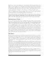
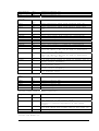
F12(L94N_4)
F13(L94P_4)
F14
U12
V12
E4
General purpose I/O
General purpose I/O
General purpose I/O
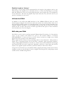
Description
OSC0
OSC1
OSC2
FPGA
pin
C5
B6
E9
OSC3
E10
CLKIN0
CLKIN1
CLKI2
CLKI3
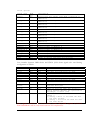
Clocks
Signal name
User
User
User
Osc
User
Osc
Oscillator input from socketed Xtal Osc
Oscillator input from socketed Xtal Osc
Oscillator input from surface mount Xtal
F4
F3
B4
A4
User
User
User
User
Clock
Clock
Clock
Clock
CLKOUT
E3
User Clock output to connector (unbuffered)
GCLK2
V20
A11
&
GCLK3
T19
C11
&
FCLK0
D2
DOCLK/GCLKx
W12
F1CLK
E1
DICLK/GCLKx
Y11
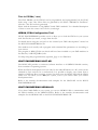
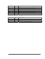
LEDs
Signal name
LED0
LED1
LED2
LED3
LED4
FPGA
pin
H3
J1
L5
J5
J2
Oscillator input from surface mount Xtal
input
input
input
input
from
from
from
from
connector
connector
connector
connector
(unbuffered)
(unbuffered)
(buffered)
(buffered)
Loop to allow user to drive a clock from V20
into A11 where a DLL can be used to distribute
the clock to the logic.
Loop to allow user to drive a clock from T19
into C11 where a DLL can be used to distribute
the clock to the logic.
Repeated from above
O/P FIFO Clock output to input of buffer. Use to
drive correct frequency.
O/P FIFO Clock output of buffer – use with DLL
for internal logic
I/P FIFO Clock output to input of buffer. Use to
drive correct frequency.
I/P FIFO Clock output of buffer – use with DLL
for internal logic
Description
General
General
General
General
General
Purpose
Purpose
Purpose
Purpose
Purpose
LED
LED
LED
LED
LED
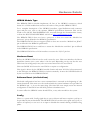
Control connections to HERON connectors
Signal name
ADDR/FLAGSEL
FPGA
pin
F12
BOOTEN
G1
UDPRES
H4
RESET
CONFIG
E15
E16
Description
Selector driven by Carrier board to determine
the function of the almost flags
This module can drive this low if it wishes the
carrier to operate regardless of the Config
signal
This module can drive this to reset the carrier
YOU MUST DRIVE THIS SIGNAL HIGH IF NOT USING IT!
Reset input from Carrier card
Open collector signal
Carrier and Module ID
63
HUNT ENGINEERING HERON-FPGA3 USER MANUAL