1
Source: Photonics Essentials
Part
I
Introductory Concepts
Downloaded from Digital Engineering Library @ McGraw-Hill (www.digitalengineeringlibrary.com)
Copyright © 2004 The McGraw-Hill Companies. All rights reserved.
Any use is subject to the Terms of Use as given at the website.
Introductory Concepts
Downloaded from Digital Engineering Library @ McGraw-Hill (www.digitalengineeringlibrary.com)
Copyright © 2004 The McGraw-Hill Companies. All rights reserved.
Any use is subject to the Terms of Use as given at the website.
Source: Photonics Essentials
Chapter
1
Introduction
Photons have been around ever since the Big Bang, which is a long
time. Photons, by definition, are always on the move: 3 × 1010 cm/sec
in air. Some of the important milestones in the history of the human
civilization are those at which we have improved our ability to control
the movement of photons. A few notable examples are the control of
fire, the design of lenses, the conception of Maxwell’s equations, the
invention of photography, broadcast radio, and the laser.
Photonics is the study of how photons and electronics interact, how
electrical current can be used to create photons as in a semiconductor
laser diode, and how photons can create an electrical current, as in a
solar cell. The field of photonics is in its infancy. Great discoveries remain to be made in using photonics to improve our lives.
The list of applications in photonics is long. Some of the rapidly
growing areas are:
Ecology:
Solar cell energy generation
Air quality and pollution monitoring
Imaging:
Camcorders
Satellite weather pictures
Digital cameras
Night vision
Military surveillance
3
Downloaded from Digital Engineering Library @ McGraw-Hill (www.digitalengineeringlibrary.com)
Copyright © 2004 The McGraw-Hill Companies. All rights reserved.
Any use is subject to the Terms of Use as given at the website.
Introduction
4
Introductory Concepts
Information displays:
Computer terminals
Traffic signals
Operating displays in automobiles and appliances
Information storage:
CD-ROM
DVD
Life Sciences:
Identification of molecules and proteins
Lighting
Medicine:
Minimally invasive diagnostics
Photodynamic chemotherapy
Telecommunications:
Lasers
Photodetectors
Light modulators
Telecommunications is an application of considerable activity and
economic importance because of the transformation of the world-wide
communications network from one that used to support only voice
traffic to one that now supports media transmitted through the Internet, including voice, data, music, and video. Of course, in the digital
world these different media are all transmitted by ones and zeros.
However, if a picture can be said to be worth more than a thousand
words, a transmitted picture counts for about a million words. The
growth of the internet and its capacity to transmit both images and
sound has been made possible only because of the vast improvements
in speed and capacity of fiber optic telecommunications. At the heart
of this revolution are the semiconductor laser, fast light modulators,
photodiodes, and communications-grade optical fiber.
From this text you can learn what makes these key devices work
and how they perform. Laboratory measurements are emphasized for
an important reason: there are many different kinds of photonic devices, but only a few basic characterization measurements. When you
learn these laboratory techniques, you can measure and understand
almost any kind of device. The experiments are based on components
that you can find easily in any electronics store. This means that the
laboratory fees should be reasonable, and that you can quickly find a
replacement device when you need one.
This course is an excellent preparation for subsequent work in the
Downloaded from Digital Engineering Library @ McGraw-Hill (www.digitalengineeringlibrary.com)
Copyright © 2004 The McGraw-Hill Companies. All rights reserved.
Any use is subject to the Terms of Use as given at the website.
Introduction
Introduction
5
physics of semiconductor devices, the design of biomedical instrumentation, optical fiber telecommunications, sensors, and micro
opto-electro mechanical systems (MOEMS). You may also want to
consider a summer internship as a test and measurement engineer
with one of the growing number of start-up companies in the optoelectronics industry.
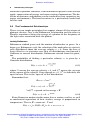
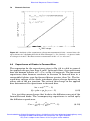
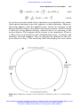
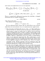
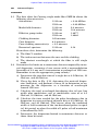
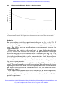
The largest market for photonic devices today is the telecommunications industry. Historically, this industry has been growing at
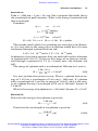
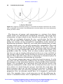
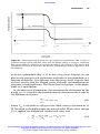
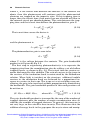
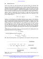
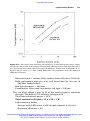
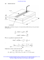
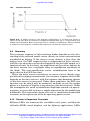
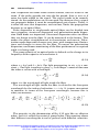
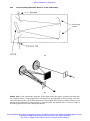
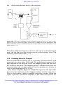
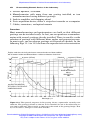
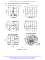
about 5% per year. The development of the optical fiber and the internet have changed all that (see Fig. 1-1).
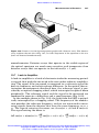
An optical fiber is generally a thin strand of glass that is used to
carry a beam of light. Once the light is introduced in the fiber, by using a lens, for example, it can only escape by propagating to the other
end of the fiber. The light beam is prevented from leaking out of the
sidewalls by an effect called total internal reflection. Thus, the fiber
acts as a guide for photons. When engineers showed that sending
high-speed communications by light waves was far superior to sending communications by electricity, growth rates in the industry
1012
OPTICAL
FIBER
SYSTEMS
10
10
108
{
Multi-channel
(WDM)
Single channel
(ETDM)
Communication
Satellites
106
Advanced
coaxial and
microwave systems
{
Relative Information Capacity (bit/s)
1014
104
102
Early coaxial cable links
Carrier Telephony first used 12 voice
channels on one wire pair
Telephone lines first constructed
100
10–2
1880 1900
1920
1940
1960
1980
2000
2020
2040
Year
Figure 1.1. The growth of telecommunications systems got a big jolt with the deployment
of optical fibers in 1980, creating the first optical fiber telecommunications networks. There
was another big jolt in 1990 when optical amplifiers were rediscovered and adapted to optical fiber telecommunications. This implemented multiple wavelength transmission (wavelength-division multiplexing) and made it possible for the Internet to grow.
Downloaded from Digital Engineering Library @ McGraw-Hill (www.digitalengineeringlibrary.com)
Copyright © 2004 The McGraw-Hill Companies. All rights reserved.
Any use is subject to the Terms of Use as given at the website.
Introduction
6
Introductory Concepts
changed dramatically, as can be seen in Fig. 1.1. This is the definition
of a disruptive technology.
An important side effect of this growth is that the composition of
the telecommunications industry is changing rapidly. Old-line companies, like Alcatel, Lucent, and Philips, that were masters at handling
slow growth and predictable schedules for deployment of new technology are being pushed to the sidelines. For example, Alcatel has recently announced that it intends to own no factories by 2010. These
are being replaced in the photonic devices industry sector by a very
large number of smaller companies, many of which have been in business for only a few years. Not all of these companies will succeed.
Making a career in the photonics industry is both exciting and punctuated occasionally by moments of instability provoked by the reorganization of this industry resulting from the implementation of new
technologies, take-overs, and creation of new start-up companies. Fortunately, there is a strong and steady growth rate, much greater than
5%, that is underlying this effervescence. To succeed, you need to
keep a close watch on both the technology and the opportunities.
Downloaded from Digital Engineering Library @ McGraw-Hill (www.digitalengineeringlibrary.com)
Copyright © 2004 The McGraw-Hill Companies. All rights reserved.
Any use is subject to the Terms of Use as given at the website.
Source: Photonics Essentials
Chapter
2
Electrons and Photons
2.1
Introduction
You will discover by measurement that all p-n diodes are sensitive to
light, even if they are intended for some other application. A photodiode is a simple and inexpensive component that you will use to measure the particle behavior of light. This is a fundamental quantummechanical property of matter, and is the effect for which Albert Einstein was awarded the Nobel Prize in physics in 1921.
Photonic devices are used to convert photons to electrons and viceversa. Photons and electrons are two of the basic quantum-mechanical particles. Like all quantum-mechanical particles, electrons and
photons also behave like waves.
In this chapter, you will learn about the wave-like and particle-like
aspects of the behavior of electrons and photons. Each electron that
carries current in a semiconductor is spread out over many thousands
of atoms; that is, it is delocalized. Trying to specify its position or its
velocity is a hopeless task. Furthermore, the semiconductor is full of
many absolutely identical electrons. They are all moving around at a
frenetic pace. Clearly, a different approach is needed.
An important new idea in this chapter is to introduce a “road map”
for electrons in a semiconductor. It tells you what states the electrons
are allowed to occupy, just as a road map tells you where the roads
are located that cars may travel on. The road map for electrons does
not tell you where the electrons are or how fast they are moving, just
as a roadmap for cars does not tell you where the cars are or how fast
they are moving. This road map is called a band structure.
Position and velocity are not very useful ideas for describing either
7
Downloaded from Digital Engineering Library @ McGraw-Hill (www.digitalengineeringlibrary.com)
Copyright © 2004 The McGraw-Hill Companies. All rights reserved.
Any use is subject to the Terms of Use as given at the website.
Electrons and Photons
8
Introductory Concepts
electrons or photons. However, two fundamental physical laws always
apply: conservation of energy and conservation of momentum. The behavior of electrons and photons can be tracked by their respective energies and momenta. The band structure is a particularly useful tool
for this task.
2.2
The Fundamental Relationships
There are two simple principles that support almost all the science of
photonic devices. One is the Boltzmann relationship and the other is
Planck’s equation relating the energy of a photon to the frequency of
the light wave associated with the photon.
Ludwig Boltzmann
Boltzmann studied gases and the motion of molecules in gases. In a
dense gas, Boltzmann said, the velocities of the molecules are statistically distributed about the average velocity v0 = 0. Since the Law of
Large Numbers in statistics says that all distributions tend toward a
Gaussian or normal distribution, Boltzmann started from this point,
too.
The probability of finding a particular velocity v1 is given by a
Gaussian distribution:
2
–(v1 – v0)
苶苶
具v2典
Pr(v = v1) = A · e ᎏ
(2.1)
where 苶
v0苶 means the average velocity = 0, and 具v
苶2苶典 means the average
苶2苶典 is definitely not
of the square of the velocity. Even though v
苶0苶 = 0, 具v
equal to zero. This is the “spread” of the distribution.
Remember that:
Ekinetic = 1–2 mv2
1 m(v 2)
––
1
2
ᎏ
Pr(v = v1) = A · e –12m具v苶2苶典
1
–
2
m具苶v
苶2苶典苶 = spread in the energy = 苶
E
Pr(v = v1) = A · e–(E/E
苶)
(2.2)
From Brownian motion studies more than a century earlier, as well
as mechanical equivalent of heat studies, energy is proportional to
temperature. That is, E
苶 = constant · T and
Pr(v = v1) = Pr(E = E1) = A · e–(E/constant · T)
Downloaded from Digital Engineering Library @ McGraw-Hill (www.digitalengineeringlibrary.com)
Copyright © 2004 The McGraw-Hill Companies. All rights reserved.
Any use is subject to the Terms of Use as given at the website.
Electrons and Photons
Electrons and Photons
9
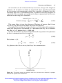
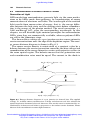
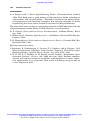
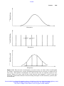
Figure 2.1. A schematic picture of a collection of atoms in a gas. The arrows give the
magnitude and direction of the velocity of each atom. If the gas is contained in a bottle on
your lab bench, then the average velocity of the atoms relative to you is 0. However, the
average of the square of the velocity is a positive number.
So, what is this constant? Boltzmann’s constant, of course!
Pr(E = E1) = A · e–(E/kBT)
kBT ⬵ 0.026 eV @ 295 K = room temp
(2.3)
If the total number of gas molecules in the bottle is NT, the number
of molecules having energy E1 is given by the total number of molecules times the probability that a molecule has energy E1:
n(E1) = NTPr(E = E1) = NT · e–(E1/kBT)
(2.4)
The number of molecules at energy E2 relative to those at energy E1
is readily expressed:
n(E2)
ᎏ = e–(E2–E1)/kBT
n(E1)
(2.5)
The Boltzmann relation given in Eq. 2.5 is a fundamental tool that
you use to determine how photonic devices operate. The Boltzmann
relation can be applied to electrons as well as to molecules, provided
that these electrons is are equilibrium. With suitable and simple modifications, it is possible to use this relationship under nonequilibrium
conditions. The current–voltage expression for a p-n diode is exactly
that adjustment. We will use this tool over and over throughout this
book. Its importance cannot be overestimated.
Downloaded from Digital Engineering Library @ McGraw-Hill (www.digitalengineeringlibrary.com)
Copyright © 2004 The McGraw-Hill Companies. All rights reserved.
Any use is subject to the Terms of Use as given at the website.
Electrons and Photons
10
Introductory Concepts
2.3
Properties of Photons
a. According to Maxwell, light is an electromagnetic wave.
b. According to Michelson and Morley, light always travels at a constant speed, c.
c. speed of light = c = wavelength × frequency = f ~ 3 × 1010 cm/sec
d. visible light:
400 nm < < 700 nm (400 nm = blue, 700 nm = red)
near infrared:
700 nm < < 2000 nm
There are many important applications in the visible and nearinfrared regions of the spectrum, including the wavelengths that optimize optical fiber communications. The most important properties of
optical fibers for communications are attenuation of the signal by absorption and distortion of the signal (noise).
High-performance optical fibers are made from glass. Attenuation
is caused by fluctuations in the density of the glass on the atomic
scale and from residual concentrations of water molecules. The water
molecules absorb light near specific wavelengths. In between these
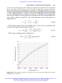
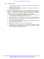
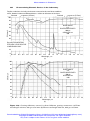
wavelengths, windows of lower attenuation are formed at = 1300
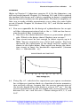
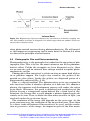
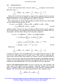
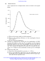
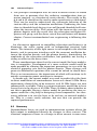
nm and 1500 nm. A good picture of this situation is shown in Fig.
2.2 for state of the art optical fibers. The properties of several types of
fibers, all of which are made by chemical vapor deposition, are shown.
The properties of optical fibers are covered in more detail in Chapter
9.
Another important application for infrared wavelengths is night vision binoculars. These instruments are composed of detectors that image the infrared heat radiation from objects and convert this signal to
a visible image so that the wearer can see in the dark.
Light beams behave like waves, and the wave properties of light are
easy to observe:
앫
앫
앫
앫
앫
diffraction effects
dispersion effects; for example, a rainbow
interference effects
wavelength
frequency
Light beams also display effects associated with particles. These effects are not as apparent in everyday experience. In the laboratory,
you will observe this behavior often.
Downloaded from Digital Engineering Library @ McGraw-Hill (www.digitalengineeringlibrary.com)
Copyright © 2004 The McGraw-Hill Companies. All rights reserved.
Any use is subject to the Terms of Use as given at the website.
Electrons and Photons
Electrons and Photons
11
Figure 2.2. Optical fibers are made of glass and can be very transparent if the glass is
pure. At 1500 nm, the loss is about 0.2 dB per kilometer. This means that a kilometer of
optical fiber is about as transparent as an ordinary windowpane. Fibers are drawn like taffy
from a preform. The properties of preforms made in three different ways are shown: vapor
axial deposition, outside vapor deposition, and inside vapor deposition. The large loss
peak at 1400 nm is the result of absorption by the first harmonic of residual OH molecules
in the glass. Please see Chapter 9 for more details. (Adapted from D. Keck et al., Proc.
SPIE, by permission.
Let us look at Planck’s study of incandescent radiation.
Observation: when things get hot, they begin to glow. As they get
hotter, (1) they glow more brightly and (2) the color of the glow
changes. We can measure the color of the glow by the frequency of the
light. So there seems to be a relationship between temperature and
frequency (color).
Exercise 2.1
If you have an electric heating appliance, you can try the following experiment. After turning off the room lights, turn on the appliance and
watch it as it heats up. Record your observations.
Note: Some people have sensitivity to infrared wavelengths beyond
the range of normal vision. According to Edwin Land, inventor of the
Polaroid camera, who studied this effect, the “color” associated with
Downloaded from Digital Engineering Library @ McGraw-Hill (www.digitalengineeringlibrary.com)
Copyright © 2004 The McGraw-Hill Companies. All rights reserved.
Any use is subject to the Terms of Use as given at the website.
Electrons and Photons
12
Introductory Concepts
this sensitivity is yellow. It appears just before the dark red glow of
the heating element appears in the visible range as it warms up. In
my classes, this effect is seen by about one out of thirty students. Sensitivity does not appear to depend on age or sex.
Planck’s proposition was that temperature is proportional to frequency. But Boltzmann already knew that temperature is proportional to energy. Therefore, we conclude that color is proportional to energy. As the energy goes up, how does the frequency change?
Remembering that f = c, as the energy gets larger, does the wavelength increase or decrease? As the energy gets larger, does the frequency increase or decrease?
So, of the two things that characterize light, and f, which one is
proportional to the energy? As the energy goes up, the wavelength
gets shorter or smaller. However, the frequency has to increase because f = c. Thus, energy is proportional to frequency:
E = hf
(2.6)
h, of course, is Planck’s constant.
Energy in a monochromatic beam of red light equal to n · h · f(red
light), where n is the amplitude, or the number of vibrations, each one
of which carries hf of energy:
energy = 冱 hf · nf
over all frequencies
f
where nf is the number of photons distributed according to Bose–Einstein statistics:
冢
1
nf = const · ᎏᎏ
hf/kBT
e
–1
冣
(2.7)
When hf > kBT, such as in the case of an incandescent body like a
stove element, nf is distributed to a good approximation by Boltzmann’s law.
Some important results obtained so far are:
1. Boltzmann’s law. For a group of electrons at equilbrium,
n(E2)
ᎏ = e–(E2–E1)/kBT
n(E1)
2. Energy is proportional to frequency: E = hf, where h is Planck’s
constant, equal to 6.63 × 10⁻³⁴ joule-sec.
Downloaded from Digital Engineering Library @ McGraw-Hill (www.digitalengineeringlibrary.com)
Copyright © 2004 The McGraw-Hill Companies. All rights reserved.
Any use is subject to the Terms of Use as given at the website.
Electrons and Photons
Electrons and Photons
13
Exercise 2.2
Take = 1000 nm = 1 m = 10–4 cm. For a tungsten light bulb, this is
the wavelength of peak intensity. What is the energy associated with
this wavelength?
Procedure:
f = c,
or
f = c/
3 · 1010 cm/sec
f ⬵ ᎏᎏ
10–4 cm
f = 3 · 1014/sec . . whew!!!
E = 6.6 · 10–34 × 3 · 10–14 = 1.98 · 10–19 joules
This sounds small, which it is according our everyday scale. However, it is very close to the energy that an electron would have if it were
accelerated through a potential of one volt:
1 eV = 1.6 · 10–19 coul × 1 V = 1.6 · 10–19 joule
In photonics, the typical energies that you work with involve electrons
in a potential of 1 or 2 V. So we use the energy of an electron accelerated through a potential of 1 V as a handy unit—the electron volt
(eV).
The energy of a photon with a wavelength of 1000 nm (or 1 m) is
1.98 · 10–19
E = ᎏᎏ
= 1.24 eV
1.6 · 10–19
(2.8)
It is easy to show that reverse is true. That is, a photon with an energy of 1 eV has a wavelength of 1.24 m (= 1240 nm). If a photon
with a wavelength of 1 m has an energy of 1.24 eV, what is the energy of a photon having a wavelength of 0.5 m (= 500 nm)? Answer: E
= 2.48 eV.
What is the energy of red photons ( = 612 nm)? Answer: E = 2.0 eV.
Exercise 2.3
Prove that the energy of any photon is given by
1.24 m
E = ᎏᎏ eV
(2.9)
Prove that the wavelength of any photon is given by
1.24 eV
= ᎏ m
E
(2.20)
Downloaded from Digital Engineering Library @ McGraw-Hill (www.digitalengineeringlibrary.com)
Copyright © 2004 The McGraw-Hill Companies. All rights reserved.
Any use is subject to the Terms of Use as given at the website.
Electrons and Photons
14
Introductory Concepts
Since photons always travel at the speed of light, it is natural to
think about the flow of energy or power in a light beam. Power is
measured in watts:
Watts = power that comes out of the light bulb = energy/sec
Watts = number of photons of frequency f/sec
× energy, summed over all f
Power = 冱 nf · Ef
f
So the total power is made up of the sum of all these little packets of
E = hf
It is sometimes more convenient in many applications to use angular frequency instead of regular frequency:
= 2f
To make everything work out right you have to divide Planck’s constant by 2:
h/2 씮 ß
E = ß
In photonics, you will use and E almost always. Rarely will you
calculate f. The most important reason for this is experimental in origin. There are no instruments that measure frequency of photons directly.
2.4
Properties of Electrons
Electrons are the ONICS of photONICS. Electrons can interact with
photons one at a time (mostly) through the medium of a semiconductor crystal. When a semiconductor absorbs a photon, the energy of the
photon can be transferred to an electron as potential energy. When
the electron loses potential energy, the semiconductor can account for
the energy difference by emitting a photon.
Exercise 2.4
A photon with energy 1.5 eV strikes GaAs. The energy is absorbed by
breaking one bond, promoting one electron from a bonding state (valence band) to an antibonding state (conduction band), and leaving a
vacant state (hole) in the valence band. Some time later, the electron
recombines with the hole, completing the bond and releasing a photon
of 1.42 eV, the bonding energy of GaAs at room temperature.
Downloaded from Digital Engineering Library @ McGraw-Hill (www.digitalengineeringlibrary.com)
Copyright © 2004 The McGraw-Hill Companies. All rights reserved.
Any use is subject to the Terms of Use as given at the website.
Electrons and Photons
Electrons and Photons
15
An electron can be characterized by its mass, charge and magnetic
moment, all of which are fixed in magnitude. It is also characterized
by its energy and momentum, which are variable. Although the electron does not have a well-defined size, it behaves in many respects as
a particle. For example, we could write down expressions for the momentum and energy of a baseball:
momentum = mv = p
p2
1
(mv)2
kinetic energy = ᎏ mv2 = ᎏ = ᎏ
2
2m
2m
(2.21)
The same thing is true for electrons. Photons, of course, don’t have
any mass. So this equation does not work for photons.
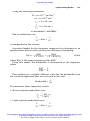
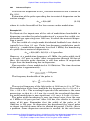
A graph of the energy of a free electron as a function of its momentum, just like that of a baseball, is a parabola (see Fig. 2.3). Remember that a 1 eV photon has =1240 nm.
On the other hand, we know from Maxwell’s equations that photons
do have a momentum that is equal to
hf
E
p= ᎏ = ᎏ
c
c
(2.22)
But, since c = f,
h
p = ᎏ = ßk,
where
2
k= ᎏ
(2.23)
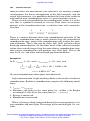
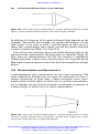
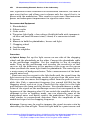
ENERGY
So, photons don’t have mass, but they have momentum.
+
MOMENTUM
–
Figure 2.3. The kinetic energy of a particle with mass, like that of an electron, is proportional to the square of its momentum.
Downloaded from Digital Engineering Library @ McGraw-Hill (www.digitalengineeringlibrary.com)
Copyright © 2004 The McGraw-Hill Companies. All rights reserved.
Any use is subject to the Terms of Use as given at the website.
Electrons and Photons
16
Introductory Concepts
Electrons have momentum, but can they have a wavelength? Well if
your name were Prince Louis-Victor, Duke de Broglie, and the year
was 1924, maybe such an idea would not seem so strange. If this were
the case, then the energy of an electron would be
1
h2
E= ᎏ · ᎏ
2m 2
Using this equation, you could actually calculate the wavelength if
you knew the electron energy. Suppose your electron has an energy of
1 eV. This is the energy of an electron that falls through a potential of
1 V.
1 eV = 1.6 × 10⁻¹⁹ joules
6.6 × 10⁻³⁴ joule-sec
h
= ᎏ = ᎏᎏᎏᎏᎏ
= 12 Å
–19
兹苶
2苶
m苶
E
兹2
苶苶·苶
9苶
×苶
10
苶–3
苶1苶k
苶g
苶苶·苶
1.6
苶苶
×苶
10
苶苶
苶jo
苶u
苶le
苶s苶
In 1929, de Broglie received the Nobel prize for this revolutionary
idea. His reasoning was different from the simple analysis above, and
involved little math, not to mention Maxwell’s equations. His insight
was based on an analogy with his everyday experience and is presented later on in Section 2.6. Nearly ten years later, in 1937, the Nobel
prize was awarded to Clint Davisson for his observation of electron
diffraction, a property of electrons that can be described only by its
fundamental wave-like nature. His lab partner, Lester Germer, got
left out of the prize list, a mystery to this day.
The work of Davisson and Germer led directly to the invention of
the electron microscope, a widely used instrument in all branches of
materials physics and engineering.
For a 1 eV photon, = 12,400 Å
For a 1 eV electron, = 12 Å
photon
At 1 eV energy (only), ᎏ = 1000
electron
This ratio depends on the electron energy. But 1 eV is characteristic of
electrons in solids. What does this mean?
Relative to the electron, the photon has mostly energy, but not very
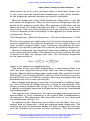
much momentum. We can see this on the diagram of energy and momentum (Fig. 2.4).
Except for the uninteresting case in which E = 0, the energy momentum curves for free electrons and photons do not intersect. That
is: there is no point on the curves where the energy and momentum of
an electron are equal to the energy and momentum of a photon. This
Downloaded from Digital Engineering Library @ McGraw-Hill (www.digitalengineeringlibrary.com)
Copyright © 2004 The McGraw-Hill Companies. All rights reserved.
Any use is subject to the Terms of Use as given at the website.
Electrons and Photons
Electrons and Photons
17
Energy
photon
electron
+
MOMENTUM
–
Figure 2.4. The energy of a photon is linearly proportional to its momentum. When plotted
on the same graph as that for an electron, the energy–momentum relationship for a photon
looks like a vertical line.
means that a free electron and a photon cannot interact with each
other. However, in a solid material the situation is different. Electrons and photons can interact because the host material can supply
the momentum that is missing in the case of a free electron and a photon. This is discussed in more detail in Section 2.7.
Imagine a vapor of single atoms of the same element. Before atomic
bonding occurs, the constituent atoms are “free” to wander around.
They are in an antibonding state. We could take silicon as an example. When two such free silicon atoms meet, they may bond together.
They will do so because the bonding state is at a lower energy than
what existed previously. The valence electrons have thus fallen into
some kind of potential well, and to do so they gave up some of their
energy. This energy that separates the bonding state from the higher
energy antibonding state is called the bonding energy. In silicon, this
energy difference is about 1 eV.
If a photon comes along, or if the thermal energy is large enough,
one of those bonds might happen to break and now there would be an
electron that is promoted from the bonding state to the antibonding
state. Of course, if all the bonds were broken the silicon would melt.
But what does the situation look like for us? At room temperature in
perfect silicon are there any broken bonds? How could you estimate
this?
Downloaded from Digital Engineering Library @ McGraw-Hill (www.digitalengineeringlibrary.com)
Copyright © 2004 The McGraw-Hill Companies. All rights reserved.
Any use is subject to the Terms of Use as given at the website.
Electrons and Photons
18
Introductory Concepts
Exercise 2.5
For each broken bond in a perfect crystal of silicon, an electron is promoted from the valence band to the conduction band. Using Boltzmann statistics you can write:
nantibonding
ᎏᎏ = e–⌬E/kT
nbonding
At room temperature, we will approximate kT by 0.025 eV,
nantibonding
ᎏᎏᎏ
ᎏ = e–1/0.025 = e–40
⬇ 1024 atoms/cm3
nantibonding ⬇ e–40 · 1024 = ??
(2.24)
This is an interesting number. Take the log of both sides:
log10(nantibonding) ⬇ 24 – 40log10(e) = 24 – (40)(0.4) = 24 – 16 = 8
nantibonding ⬇ 108 bonds/cm3
This back of the envelope estimate shows that on the average a
semiconductor whose band gap (= antibonding – bonding energies) = 1
eV will have about 108 broken bonds per cm3. A more detailed calculation for silicon based on the same principles gives ~1010 cm–3 broken
bonds at room temperature.
When the bond is broken, the electron is promoted from the valence
band, or bonding orbitals to the conduction band or antibonding orbitals. Another name of the conduction band is simply the set of unoccupied levels that are closest in energy to the valence band levels.
When the bonds are not broken, they act like springs that hold the
atoms in the crystal at the right distance from each other. These
springs vibrate as a way of storing the thermal energy of the crystal.
The vibrational energy of each atom = 1–2 kT for each degree of freedom,
or 3–2 kT. So the average vibrational energy at room temperature is
about 40 meV. These vibrations have a frequency and a wavelength
that are related by the speed of sound:
vs = f
The speed of sound in solid materials is about 105 cm/sec = 103 m/sec.
Exercise 2.6
What is the ratio of vs to the speed of light?
Downloaded from Digital Engineering Library @ McGraw-Hill (www.digitalengineeringlibrary.com)
Copyright © 2004 The McGraw-Hill Companies. All rights reserved.
Any use is subject to the Terms of Use as given at the website.
Electrons and Photons
Electrons and Photons
19
vs /c ~ 105/1010 ~ 10–5
So for the same frequency f (= same energy),
s
ᎏ = ____________?
What is the frequency of a 40 meV vibration?
(40 × 10–3)(1.6 × 10⁻¹⁹)
E
f = ᎏ = ᎏᎏᎏ
= 9 × 1012 = 1013 Hz
h
6.6 × 10⁻³⁴
(2.27)
What is the wavelength ?
= vs /f = 105/1013 = 10–8 cm
Well, this is only a few times larger than the lattice parameter of Si.
Does this make sense?
The lower limit on the wavelength is the interatomic distance
which is about 0.12 × 10⁻⁸ cm in silicon. So lattice vibrations have a
wavelength that is an integral multiple of the lattice parameter.
These vibrational quanta are called phonons. They are important because they allow the semiconductor to reach equilibrium.
To summarize our story so far:
Wavelength of a 1 eV electron = 12 Å
Wavelength of a 1 eV photon = 1240 nm
= 1000 × electron
(only true around 1 eV!)
So, what is the wavelength of a 1 eV phonon? The answer is, a 1 eV
phonon does not exist. It cannot exist because its wavelength would
be much smaller than the separation between atoms, and the phonon
represents vibrations of atoms. However, the wavelength of a 40 m eV
phonon is about the same as that for the 1 eV electron.
Since momentum = h/, at room temperature, the momentum of a
typical phonon is similar to the momentum of 1 eV electron.
As electrons move around in the semiconductor, they need to conserve energy and momentum. In this never ending struggle, the
phonon acts as a source of momentum that contributes very little energy, whereas the photon can contribute energy with very little momentum. As the electron interacts with light, the electric field, etc.,
both phonons and photons interact with the electron so that both energy and momentum are conserved.
Downloaded from Digital Engineering Library @ McGraw-Hill (www.digitalengineeringlibrary.com)
Copyright © 2004 The McGraw-Hill Companies. All rights reserved.
Any use is subject to the Terms of Use as given at the website.
Electrons and Photons
20
Introductory Concepts
2.5
Some History
The proposition of de Broglie (pronounced duh Broy-yuh) was absolutely revolutionary, but not at all obvious at the time. The principal result of his idea was to open the way for the development of
Schrödinger’s wave equation and the first quantitative description of
the behavior of electrons and atoms. de Broglie had the advantage
that he was a student. He knew a little bit, but not too much. This feature was key, in my opinion, because it allowed him to see the forest
in spite of the trees. Later in life, when he knew more, he was much
less productive, and because of his celebrity, his views took on an importance unsupported by their content alone.
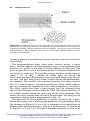
de Broglie defended his thesis in late November of 1924. The cover
page is shown in Fig. 2.5. The thesis is short, about 100 pages in all.
Almost all of the chapters are concerned with the effect of special relativity on the properties of various fundamental particles such as the
energy and phase of a propagating light beam.
In Chapter 3 of the thesis, there is an abrupt change of subject, and
de Broglie addresses hypothesis proposed by Bohr to explain the existence of discrete atomic energy levels. Seven years earlier, Neils Bohr
proposed that the electrons in atoms traveled in stable orbits, thus allowing atoms to have long lifetimes, an experimental truth we all recognize. The condition originally proposed by Bohr was
h
m0R2 = n ᎏ
2
(2.28)
where m is the mass of the electron, the angular frequency of rotation around the atom, and R the radius of its orbit. For a circular orbit, = v/R, and Bohr’s condition becomes
h
m0vR = n ᎏ
2
(2.29)
This has the simple interpretation that the angular momentum of the
electron (= mvR) is quantized in units of
h
ß= ᎏ
2
However, in 1924 there was no idea about why this quantization occurred, or what properties of the electron assured this behavior.
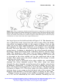
On page 44 of his thesis (Fig. 2.6), de Broglie offered an interpretation that was consistent with his everyday experience: the Bohr condition was similar to the behavior of waves of water in a closed circular
tank. Stable states occur when there are standing waves. The condi-
Downloaded from Digital Engineering Library @ McGraw-Hill (www.digitalengineeringlibrary.com)
Copyright © 2004 The McGraw-Hill Companies. All rights reserved.
Any use is subject to the Terms of Use as given at the website.
Electrons and Photons
Electrons and Photons
21
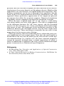
Figure 2.5. Cover page for the doctoral thesis of Louis de Broglie. Each doctoral candidate had to write on two subjects: one chosen by the candidate, and one assigned. The title of his chosen subject is: “Research on the Theory of Quanta.”
Downloaded from Digital Engineering Library @ McGraw-Hill (www.digitalengineeringlibrary.com)
Copyright © 2004 The McGraw-Hill Companies. All rights reserved.
Any use is subject to the Terms of Use as given at the website.
Electrons and Photons
22
Introductory Concepts
Figure 2.6. The proposition by de Broglie in his thesis that the stable orbits of electrons in
atoms are like waves of water in a closed circular tank. Translation of the boxed portion:
“The propagation (of the electron) is therefore analogous to that of a wave of liquid in a
tank that forms a closed path. In order to have a stable condition for the wave, it is physically evident that the length of the tank must be in resonance with the wave. In other
words, the portions of the wave that are located a full length l of the tank behind preceding
portion of the wave must be in phase with the preceding portion. The condition for resonance is l = n.”
tion for the existence of a standing wave is that the length of the circuit be an integral number of wavelengths of the standing wave.
There are only certain fixed lengths of the tank that can support
standing waves. The possible tank lengths are given by the relation L
= n. The argument of de Broglie contains no equations.
If we substitute the resonance condition of de Broglie into Eq. 2.29
(remember that R = 1/2) we get:
冢 冣
l
h
m0v ᎏ = n ᎏ
2
2
m0v(n) = nh
h
m0v = ᎏ
(2.30)
Equation 2.30 says that the electron has a wavelength that is inversely proportional to its momentum. This simple equation does not
appear in de Broglie’s thesis, nor does the extension of this result to
free electrons or other particles like photons. However, de Broglie let
Downloaded from Digital Engineering Library @ McGraw-Hill (www.digitalengineeringlibrary.com)
Copyright © 2004 The McGraw-Hill Companies. All rights reserved.
Any use is subject to the Terms of Use as given at the website.
Electrons and Photons
Electrons and Photons
23
the cat out the bag so to speak, for which he was awarded the Nobel
Prize in 1929. He claimed credit in his thesis for “the first plausible
physical explanation for the condition of stable orbits as proposed by
Bohr and Sommerfeld.”
I find that the most interesting part of de Broglie’s reasoning to be
the notion that because quantization exists, there must be an associated wave behavior.
2.6 Changing Places: How Electrons Behave
in Solids
The energy momentum relationship for an electron is the same as the
energy momentum relationship for a baseball. But, because the electron has a wavelength, we can represent its behavior by a wavefunction:
⌿(k, x) = A sin(kx)
A semiconductor crystal is a periodic arrangement of atoms. The periodicity applies to all the physical properties of the crystal. This means
that the allowed values for energy and momentum have to be periodic, too:
A sin(kx) = A sin[k(x + a)], where a = the period of the crystal lattice
= A sin kx cos ka – A cos kx sin ka
This is true if
ka = 2
or
2
k= ᎏ
a
At these special k values, everything looks the same. Since everything looks the same, we just keep the central zone that has the
unique information between k = –/a and k = /a. This is called the
Brillouin zone. Brillouin was a classmate of de Broglie.
The diagram in Fig. 2.7 has its characteristic shape because of the
periodicity, or to use a more general term, the symmetry of the crystal. There are two essential components of the energy–momentum relationship in crystals of real materials: symmetry and chemistry. The
component added by chemistry is the potential added by the atoms
that make up the crystal. Si atoms have a different potential from Ge
atoms, and the energy–momentum relationship for Si is slightly different from that for Ge.
Downloaded from Digital Engineering Library @ McGraw-Hill (www.digitalengineeringlibrary.com)
Copyright © 2004 The McGraw-Hill Companies. All rights reserved.
Any use is subject to the Terms of Use as given at the website.
Electrons and Photons
24
Introductory Concepts
Figure 2.7. Diagram of electron energy as a function of electron momentum for an electron in a periodic environment. Each period of the structure reflects the same electron behavior, just like a mirror.
The diagram of energy and momentum is a picture that shows
which states are allowed to be occupied by electrons. You need extra
information to know which states actually are occupied. In Fig. 2.8,
we show an analogous diagram for cars: a road map. On this road
map we see some lines indicating roads. These lines tell you what
places (or states) can be occupied by automobiles under normal or
equilibrium conditions. However, you need more information in order
to know which states are actually occupied by automobiles. The road
map does not tell you much about the velocity of the cars, either. In
Fig. 2.8a, we see that the shape of the road map with nice straight
lines gives us some information about the terrain of the region: it is
probably rather flat. In Fig. 2.8b, we show another road map. Here
the lines are not so simple, indicating that there are rises and falls in
the terrain of this region. These changes in terrain are changes in potential. They play the same role in a road map as chemistry plays in
the energy–momentum relationship for electrons.
This energy–momentum map is called the band structure. It tells
you what are the allowed (or stable) states of energy and momentum
for electrons in the outermost band (or valence band) of the semiconductor. It is analogous to a road map that tells you the streets and
highways (allowed or stable states for an electron) that your car can
have when it is freed from the garage. Just like the road map, the
band structure does not tell you where the electron is. Rather, the
band structure tells you what the possible states are, and about the
properties that an electron would have if it occupied a particular
state. For example, from a road map you can tell the difference between a residential street and a superhighway. In addition to the lo-
Downloaded from Digital Engineering Library @ McGraw-Hill (www.digitalengineeringlibrary.com)
Copyright © 2004 The McGraw-Hill Companies. All rights reserved.
Any use is subject to the Terms of Use as given at the website.
Electrons and Photons
Electrons and Photons
25
(a)
H
H O NDA
RK
PA
Cr.
La
LA
ne
Alpi
Cr.
g
Kin
GE
RID
RD.
r.
RD.
sto
n
ADER O A L
P E SC
RD.
C
SAM
EL. 200
SAN MATEO
COUNTY
MEM. PARK
.
RD
1.1
P IN
McDONALD
OAKLAND
Y.M.C.A.
CAMP
n
Mi
E
HERITAGE
GROVE
CO. PARK
Cr.
CO. PARK
N
ES
G ULCH
SAN FRANCISCO
Y.M.C.A. CAMP
EL. 2
MINDEG
JO
d Cr.
PESCADERO
(b)
Cr
6.9
R
D
Hoffman C
r.
h en
ly C
r.
E
LAN
La Honda
EL. 405
r.
Loma
Mar
6.6
Wood
deg
o
ER
Har
r
DE
Bo
g
on
ingt
Figure 2.8. A conventional road map identifies the stable states that automobiles can occupy. The road map does not tell you where the automobiles are or how fast they are moving. The location of the states depends, in general, on the shortest distance between two
points in the context of the barriers imposed by the terrain. In (a) we show a road map of a
flat terrain. There are few potential variations and the roads are straight. (© BP-Amoco;
used by permission.) In (b) we show a road map of a more rugged terrain. This can result in
roads with many curves, or roads that deviate significantly from taking the shortest distance between two points. (© 2002 California State Automobile Association. Used by permission.)
Downloaded from Digital Engineering Library @ McGraw-Hill (www.digitalengineeringlibrary.com)
Copyright © 2004 The McGraw-Hill Companies. All rights reserved.
Any use is subject to the Terms of Use as given at the website.
Electrons and Photons
26
Introductory Concepts
Figure 2.9. The relationship between energy and momentum displays bands of energy
that an electron can have. When the electron is in a crystal, the periodic atomic potential
causes gaps to open up in this structure. The gap means that an electron is not allowed to
have these energies.
cation of these different roads, you know that the velocity of an automobile is limited to a speed of 50 km/h on a residential street, but 100
km/h on the superhighway.
The size of an electron is not well-defined, and so it is not very
meaningful to try to specify its position. A totally free electron behaves like a wave. That means it can exist over all space. Since the location of such a wave is difficult to specify, it is equally difficult to
specify its velocity.
On the other hand, energy and momentum for an electron can be
specified. Furthermore, the conditions that define the interaction of
electrons in solids with photons, phonons, or other electrons are conservation of energy and conservation of momentum. So a “road map”
that summarizes the possible states of electron energy and momentum is particularly useful.
All band structures can be divided into two groups. There are two
bands that form the band gap. If the minimum energy of the upper
band occurs at the same value of momentum as the maximum energy
of the lower band, the corresponding material has a direct band gap.
Such a band structure is shown in Fig. 2.9. For all other situations,
the corresponding material has an indirect band gap.
Whether a material has a direct band gap or an indirect band gap depends entirely on the crystalline potential that splits apart the bands.
Downloaded from Digital Engineering Library @ McGraw-Hill (www.digitalengineeringlibrary.com)
Copyright © 2004 The McGraw-Hill Companies. All rights reserved.
Any use is subject to the Terms of Use as given at the website.
Electrons and Photons
Electrons and Photons
27
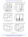
Figure 2.10. In this sequence of calculations, we show how the periodic potential modifies
the energy–momentum relationship for a real three-dimensional semiconductor, GaAs. In
the first frame, you can clearly see the parabolic relationship between energy on the vertical axis and momentum on the horizontal axis. In succeeding frames, we add the periodic
potential due to the actual atoms. This causes the crossings to separate. By the time we
arrive at GaAs, there is a band gap between the valence band and the conduction band.
Because the minimum of the conduction band and the maximum of the valence band occur at the same value of momentum, this is a direct energy gap. GaAs, InP, GaInAsP, and
GaN are examples of direct-gap semiconductors.
This splitting is shown symbolically in Fig. 2.9. In Eqs. 2.10 and 2.11,
we show how the splitting occurs in the real band structures of GaAs
and Ge. The crystalline potential is the direct expression of the atoms
that make up the material. So, the difference between direct band gap
and indirect band gap materials is a matter of chemistry.
The band gap expresses the difference in energy between an electron
in a bonding state and an electron in an antibonding state. In the antiDownloaded from Digital Engineering Library @ McGraw-Hill (www.digitalengineeringlibrary.com)
Copyright © 2004 The McGraw-Hill Companies. All rights reserved.
Any use is subject to the Terms of Use as given at the website.
Electrons and Photons
28
Introductory Concepts
bonding state, the electron is free to carry electrical current. So this upper band, the antibonding state, is also called the conduction band. The
bonding state, or lower band, is also called the valence band.
An electron that occupies a state at the minimum energy of the conduction band can make a transition to the top of the valence band,
presuming this state is not already occupied. These two states have a
negligible difference in momentum. Energy is conserved by the emission of a photon. Since the photon provides very little momentum,
both energy and momentum can be conserved for this transition,
which is called a direct transition.
By comparison, an electron occupying a state at the bottom of the
conduction band in an indirect gap material is in a different situation.
The difference in momentum between these two states is no longer
negligible. The electron can make a transition to a state at the top of
the valence band by the emission of a photon to conserve energy, and
the simultaneous emission of a phonon to conserve momentum. This
is called an indirect transition because two steps are involved.
In the case of Fig. 2.10, there is no difference in momentum between a state at the top of the valence band and a state at the bottom
of the conduction band. In Fig. 2.11, the situation is different.
In this case, the lowest energy state in the conduction band does not
have the same momentum as the highest energy state in the valence
band. At equilibrium and at T = 0 K, all the valence band states are
occupied and none of the conduction band states are occupied. Now let
us break a bond in Ge. That means that one electron has enough extra
energy to go from a bonding state to an antibonding state. The least
amount of extra energy is the band gap energy. In germanium, this is
0.7 eV. (We use eV to measure energy so you do not have to carry
around mind-boggling powers of 10 in your calculations.) For silicon,
the indirect energy gap is 1.1 eV.
You can see from the energy band structure diagram for germanium that the electron needs to get some momentum in addition to energy to make a transition at this least energy near the band gap. So
the transition to the antibonding state is not direct. There are two
steps required: first, obtain the energy, and second, obtain at the
same time the required momentum from a physical vibration of the
crystal lattice. This is called an indirect transition and germanium is
called an indirect band gap semiconductor.
By referring to the band structure of GaAs, you can see that this
transition can be made in one step with little or no change in momentum required. This happens because the maximum valence band energy occurs at the same momentum as the minimum conduction band
energy. Since the photon can convey energy with no momentum, the
electron can absorb a single photon and make the transition across
Downloaded from Digital Engineering Library @ McGraw-Hill (www.digitalengineeringlibrary.com)
Copyright © 2004 The McGraw-Hill Companies. All rights reserved.
Any use is subject to the Terms of Use as given at the website.
Electrons and Photons
Electrons and Photons
29
Figure 2.11. In this sequence of calculations, we show how the periodic potential modifies
the energy–momentum relationship for a different semiconductor, Ge. In the first frame,
you can clearly see the parabolic relationship between energy on the vertical axis and momentum on the horizontal axis. It is identical to the first frame shown in Fig 2.10, because
we start from the same situation, the free electron. In succeeding frames we add the periodic potential due to the actual Ge atoms. This causes the crossings to separate. By the
time we arrive at Ge, there is a band gap between the valence band and the conduction
band. However, the minimum of the conduction band and the maximum of the valence
band do not occur at the same value of momentum. This is an indirect energy gap. Si and
Ge are examples of indirect-gap semiconductors.
the gap in a direct fashion. This is called a direct transition and GaAs
is called a direct gap semiconductor.
The band structure is a visual display of the states of energy and
momentum that can be occupied by an electron. Since the semiconductor crystal is a solid, we know that the states in the valence band
are nearly completely occupied by electrons. Undoped semiconductors
have just enough electrons to complete the bonding. Therefore, even
Downloaded from Digital Engineering Library @ McGraw-Hill (www.digitalengineeringlibrary.com)
Copyright © 2004 The McGraw-Hill Companies. All rights reserved.
Any use is subject to the Terms of Use as given at the website.
Electrons and Photons
30
Introductory Concepts
at room temperature, there are not very many occupied states in the
conduction band compared to the occupied states in the valence band.
Under most conditions, Boltzmann statistics can be used, as we have
done in Eqs. 2.1–2.5, to calculate the number of states in the conduction band that are occupied by electrons, or the number of empty sites
in the valence band. These are called holes.
2.7
Summary
The behavior of electrons in semiconductors at equilibrium is ruled by
the Boltzmann distribution under almost all circumstances. The Boltzmann distribution says that the probability of finding an electron with
energy Ea decreases exponentially as Ea increases. The three fundamental energy excitations in semiconductors are electrons, photons,
and phonons. We treat the indivisible units of these excitations as particles. Each particle has a wavelength that is proportional to the reciprocal of its momentum. Each particle obeys the two basic laws of conservation of energy and momentum. These two laws are the foundation
that determines all the possibilities that photonics has to offer.
The map of allowed electron states is called a band structure. For
semiconductors like GaAs and Si, the electron states are generally
filled up to and including the valence band states or the bonding
states. This is followed by an energy gap that results because there is
an energy difference between the bonding and the antibonding, or
conduction band states. If the highest energy valence band state occurs at the same momentum as the lowest energy conduction band
state, the material is called a direct band gap semiconductor. GaAs
and InP are examples of direct band gap semiconductors. If the minimum energy of the conduction band occurs at a different momentum
than the maximum energy on the valence band, then the material is
known as an indirect band gap semiconductor. Si and Ge are examples of indirect band gap materials.
The thermal energy available from the environment can act to
break bonding states. This action creates vacancies in the occupation
of the valence band called holes, because the electrons that maintained those bonds are absent. The liberated electrons are now in antibonding states in the conduction band. The Boltzmann distribution
is used to keep track of the number of electron states that are occupied in the conduction band as a function of temperature.
Bibliography
C. Cercignani, Ludwig Boltzmann, The Man Who Trusted Atoms, New York,
Oxford Univeristy Press, 1998. Boltzmann’s ideas about the direction of
Downloaded from Digital Engineering Library @ McGraw-Hill (www.digitalengineeringlibrary.com)
Copyright © 2004 The McGraw-Hill Companies. All rights reserved.
Any use is subject to the Terms of Use as given at the website.
Electrons and Photons
Electrons and Photons
31
time and statistical mechanics form the core science of the physics and the
technology semiconductor devices. These ideas were not accepted by his
peers, and this rejection may have been a factor in his suicide by hanging
in 1906. To learn more, read this book!
David Lindley, Boltzmann’s Atom: The Great Debate that Launched a Revolution in Physics, New York, Free Press, 2001.
C. R. Wie, “The Semiconductor Applet Service,” http://jas.eng.buffalo.edu/
applets/. A truly outstanding set of applets on semiconductor physics and
devices has been written by Prof. Chu R. Wie of the University of Buffalo.
Bookmark this Web site!
“The Britney’s Guide to Semiconductor Physics,” http://www.britneyspears.
ac/lasers.htm. Whether or not you are a fan of Ms. Spears, this site is an
excellent introduction to semiconductor optoelectronic devices like lasers
and new directions in photonics such as photonic crystals.
D. Halliday, R. Resnick, and K. Krane, Physics, 4th Edition, Wiley, New York,
1992. See page 883 for a discussion of the relationship E = pc.
E. Hecht, Optics, 2nd Edition, Addison-Wesley, Reading, 1987.
J. Wilson and J. Hawkes, Optoelectronics, 3rd Edition, Prentice-Hall Europe,
London, 1998.
Downloaded from Digital Engineering Library @ McGraw-Hill (www.digitalengineeringlibrary.com)
Copyright © 2004 The McGraw-Hill Companies. All rights reserved.
Any use is subject to the Terms of Use as given at the website.
Electrons and Photons
32
Introductory Concepts
Problems
2.1 A p-n junction is a metallurgical junction between two materials
having different numbers of free electrons in their respective
conduction bands. At equilibrium, Boltzmann statistics can be
applied. Use this information to determine the energy difference
in electron volts between the conduction bands on each side of
the junction if the n-side has 1018 cm–3 free electrons and on the
p-side there are 104 cm–3 electrons. Assume that the junction is
at room temperature.
2.2 We know that a photon cannot interact with a free electron because simultaneous conservation of energy and momentum is
not possible. That is, their energy band structures do not intersect. In a collision between an electron, a photon, and a phonon,
an interaction is possible. This can happen in a solid like Si or
GaAs.
a. Calculate the wavelength, the frequency, and the energy of the
phonon in silicon that will allow a 1 eV photon to transfer all its
energy to an electron. Assume that the electron is initially at
rest (E = 0) (that is, T = 0). The velocity of sound in silicon is
about 8.5 × 10³ meters per second at room temperature.
b. What is the final energy of the electron?
c. If the collision takes place in silicon at room temperature,
what is the likely initial energy of the electron?
2.3 Electrons in a semiconductor have the full electronic charge q,
but often their mass appears to be different from the free electron mass. In GaAs, for example, the effective mass of an electron is equal to 0.065 the value of the free electron mass. The
size of the effective mass depends on both the structure and the
crystalline potential of the semiconductor. Given this information:
a. Calculate the de Broglie wavelength of a conduction band
electron in GaAs, assuming a kinetic energy equal to the thermal energy at room temperature.
b. The wavelength corresponds to how many unit cells of the
crystal?
c. In three dimensions, estimate how many atoms could be
found in a sphere the diameter of which is equal to a de
Broglie wavelength in GaAs.
2.4 Show from first principles that the energy of a photon can be calculated from its wavelength by the following relationship:
Downloaded from Digital Engineering Library @ McGraw-Hill (www.digitalengineeringlibrary.com)
Copyright © 2004 The McGraw-Hill Companies. All rights reserved.
Any use is subject to the Terms of Use as given at the website.
Electrons and Photons
Electrons and Photons
33
124
E(eV) = ᎏ
(nm)
where the energy is given in electron volts and the wavelength in
nanometers.
2.5 Make a graph to scale of wavelength on the lower horizontal axis
and energy on the upper horizontal axis. The wavelength range
should vary from 200 nm to 2000 nm.
a. What is the corresponding energy range?
b. Mark the following regions:
blue light
green light
red light
1550 nm low-loss region for optical fiber telecommunications
c. Which photons have more energy, red or blue?
d. Paste a copy of this graph in your lab notebook
2.6 The energy of an electron is equal to the square of its momentum
divided by 2 times its mass. From de Broglie, we also know that
the electron behaves like a wave.
a. By taking the second derivative with respect to x of the simple
wave function ⌿(x) = A sin(kx), show that you get the following relationship:
d2
⌿(x) = –k2⌿(x)
ᎏ
dx2
b. Multiply both sides of this relationship by the appropriate
constants to derive a formula for the energy of the electron.
This formula is the basis for the Schrödinger equation, the
mathematical foundation of quantum mechanics.
2.7 Silicon has a band gap of 1.1 eV at room temperature. Using a
monochromator, you send a beam of photons with a wavelength
of 1240 nm on the surface of a silicon wafer 0.5 mm thick. Only
three things can happen: absorption, reflection, and transmission of the beam of light. Which things actually happen under
these circumstances?
2.8 When a photon passes from air into glass, its trajectory is
changed according to Snell’s law—n1 sin(1) = n2 sin(2)—and the
velocity of light is reduced by the ratio of the index of refraction
of air (n1 = 1) to that of glass (n2 = 1.5). When the photon travels
in glass it still obeys the relationship: V = f, where V is the
Downloaded from Digital Engineering Library @ McGraw-Hill (www.digitalengineeringlibrary.com)
Copyright © 2004 The McGraw-Hill Companies. All rights reserved.
Any use is subject to the Terms of Use as given at the website.
Electrons and Photons
34
Introductory Concepts
speed of light in glass = c/n2. On the other side of the equation,
the product f must also change to maintain equality. How is
this change accomplished? Does the frequency change, the wavelength change, or some combination of both? Use conservation of
energy to support your argument.
Downloaded from Digital Engineering Library @ McGraw-Hill (www.digitalengineeringlibrary.com)
Copyright © 2004 The McGraw-Hill Companies. All rights reserved.
Any use is subject to the Terms of Use as given at the website.
Source: Photonics Essentials
Part
II
Photonic Devices
Downloaded from Digital Engineering Library @ McGraw-Hill (www.digitalengineeringlibrary.com)
Copyright © 2004 The McGraw-Hill Companies. All rights reserved.
Any use is subject to the Terms of Use as given at the website.
Photonic Devices
Downloaded from Digital Engineering Library @ McGraw-Hill (www.digitalengineeringlibrary.com)
Copyright © 2004 The McGraw-Hill Companies. All rights reserved.
Any use is subject to the Terms of Use as given at the website.
Source: Photonics Essentials
Chapter
3
Photodiodes
3.1
Introduction
There are a number of solid-state devices that can generate an electric signal when they are illuminated. We can divide all these devices into two categories. In one category are the devices that convert the energy in a beam of light into an electric signal. An example
of this is the bolometer. This is really a collection of thermocouples
inside an efficient photon absorber. The energy of the photons is converted to heat, and the rise in temperature is converted by the thermocouples into an electric signal. These devices are energy detectors.
The electrical current is proportional to the energy in the optical
beam. In the second group are quantum threshold detectors. Photons
can be absorbed in these devices if the energy of a photon exceeds a
certain threshold value. All absorbed photons generate the same current, regardless of their energy above the threshold value. Photodiodes fall into this second category. Photons can be absorbed in a
photodiode if their energy exceeds the band gap energy of the photodiode material. In principle, each photon absorbed contributes one
electron to the current. This is a direct exchange of quanta—one
electron for one photon. In most photodiodes, this exchange is nearly 100% efficient.
Photodiode detectors were developed along with the transistor. Silicon is the most common photodiode material for two reasons. Silicon
photodiodes are sensitive to a range of light wavelengths that include
the region of visible light. Silicon photodiode manufacture benefits
from the same advanced processing technology used to make silicon
integrated circuits.
37
Downloaded from Digital Engineering Library @ McGraw-Hill (www.digitalengineeringlibrary.com)
Copyright © 2004 The McGraw-Hill Companies. All rights reserved.
Any use is subject to the Terms of Use as given at the website.
Photodiodes
38
Photonic Devices
In this chapter, we will develop a model for the conversion of light
into electrical current by a photodiode. Along the way, we will also develop a relationship for the current voltage relationship in a p-n junction. The p-n diode is a device that puts the Boltzmann relation to
work. So it is no surprise to find expressions like e–⌬E/kT in the relationship between voltage and current. Without any voltage applied
across the terminals of a p-n junction, there is no current. In the language of Boltzmann, the probability of finding a free electron on the pside of the junction is equal to the probability of finding a free electron
on the n-side. Thus, the energy difference must be zero. When a voltage is applied between the p-side and the n-side, the energy difference
is no longer zero, and so the probabilities are no longer the same. This
difference leads to a current in the diode.
The p-n junction is the basic device structure for all semiconductor optoelectronic devices, for example, lasers, LEDs, modulators, optical
switches, semiconductor optical amplifiers and so on. By characterizing
the electrical and optical properties of the p-n junction, much can be
learned about the internal composition and structure of the device, for
example, the band gap and the level of background impurities in the
material being used. This chapter includes results from suggested laboratory experiments that are given in Chapter 11. The problems are largely based on real data measured at the bench during these experiments.
The chapter reviews the fundamentals of photodiodes and their
electrical and optical properties (current–voltage relationship, quantum efficiency, and spectral response).
3.2
The Current–Voltage Equation for Photodiodes
A silicon photodiode can absorb photons that have an energy greater
than the band gap [Eg(Si) = 1.1 eV at room temperature]. Absorption
creates an electron in the conduction band and a hole in the valence
band. Most of this absorption takes place in neutral material, creating
one majority carrier and one minority carrier. The minority carrier will
diffuse to the p-n junction and be carried to the other side where it becomes a majority carrier, and contributes to the photocurrent. We can
determine the current–voltage relationship for a photodiode if we know
the functional dependence of the excess minority carrier concentration
as a function of position in the p-n junction. This depends on the applied voltage. The current can be obtained directly from the diffusion
equation
d
J = –qD ᎏ n(x)
dx
In order to examine the details, let us consider the energy level dia-
Downloaded from Digital Engineering Library @ McGraw-Hill (www.digitalengineeringlibrary.com)
Copyright © 2004 The McGraw-Hill Companies. All rights reserved.
Any use is subject to the Terms of Use as given at the website.
Photodiodes
Photodiodes
39
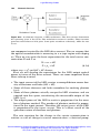
Figure 3.1. The energy-level diagram for a p-n junction at equilibrium. This is a plot of
potential energy versus distance. Note that the Fermi energy is constant, indicating
that the potential for electrons is constant throughout the structure. This means that
the electric current is 0. Note that the direction of distance for holes is opposite to that
for electrons.
gram for a photodiode (Fig. 3.1). In this energy-level diagram we can
plot out the energy levels of electrons and holes in the photodiode as a
function of distance. It is different from the energy-band diagram that
we have used to find the allowed states of energy and momentum for
electrons in semiconductors. The Fermi level is constant, so the photodiode is at equilibrium.
In the absence of illumination, the concentration of electrons on the
p-side, np0, is related to the concentration of electrons on the n-side by
the Boltzmann relation:
np0
ᎏ = e–(qVBi/kT)
nn0
(3.1)
where VBi is the built-in voltage of the diode (refer to the book by G.
W. Neudeck in the bibliography for more details). When a bias voltage
VA is applied, the Boltzmann relation still rules, and
np
np0 + ⌬n
ᎏ = ᎏᎏ = e–q[(VBi–VA)/kT]
nn
nn
(3.2)
Downloaded from Digital Engineering Library @ McGraw-Hill (www.digitalengineeringlibrary.com)
Copyright © 2004 The McGraw-Hill Companies. All rights reserved.
Any use is subject to the Terms of Use as given at the website.
Photodiodes
40
Photonic Devices
In this expression, both np and nn change to accommodate the bias
voltage VA:
np0 씮 np = np0 + ⌬n
and
nn0 씮 nn = nn0 + ⌬n
(3.3)
In the low-injection limit, which is always true for photodiodes, nn0 +
⌬n ⬵ nn0, because nn0 is many orders of magnitude larger than ⌬n. We
can use this approximation to derive the excess minority carrier density that is induced by the bias voltage at the edge of the depletion region:
⌬n = nn{e–[q(VBi–VA)/kT]} – np0 = np0 e–qVBi/kT{e–[q(VBi–VA)/kT]} – np0
⌬n = np0(eqVA/kT – 1)
(3.4)
In Eq. 3.4, note the appearance of the term –np0. This term is required to make the current 0 when the applied voltage is 0, and it is
also the origin of the dark current of the photodiode. Current is carried in the diode by both drift and diffusion. However, at the edge of
the depletion region, for example at xp = 0, the current is carried only
by diffusion. If we calculate the I–V characteristic at this point, we
can work with only one equation, the diffusion equation:
⌬n(x)
⭸
d2
ᎏ ⌬np(x) = De ᎏ
⌬n(x) – ᎏ + GL
2
⭸t
dx
e
(3.5)
This equation says that the time rate of change of the excess carrier
concentration is given by the generation rate inside the diode, less
any recombination, and plus any additional carriers generated by
light. We need to write a similar equation for the excess hole minority
carrier density on the n-side of the diode. That equation is completely
analogous to Eq. 3.4, so we can solve 3.4 and deduce the answer for
the n-side of the diode. Equation 3.4 is a second-order differential
equation for ⌬np, which is a function of distance in the diode. The generation rate of minority carriers from photon absorption is given by
GL, and the minority carrier recombination time is given by e. The
minority carrier diffusion coefficient for electrons in p-type material is
De. We will first look at steady-state conditions, and this means that:
⭸
d2
⌬n(x)
ᎏ ⌬np(x) = 0 = De ᎏ
⌬n(x) – ᎏ + GL
⭸t
dx2
e
d2
⌬n(x)
De ᎏ
⌬n(x) = ᎏ – GL
2
dx
e
d2
⌬n(x)
GL
ᎏ
⌬n(x) = ᎏ – ᎏ
2
dx
Dee
De
(3.6)
Downloaded from Digital Engineering Library @ McGraw-Hill (www.digitalengineeringlibrary.com)
Copyright © 2004 The McGraw-Hill Companies. All rights reserved.
Any use is subject to the Terms of Use as given at the website.
Photodiodes
Photodiodes
41
This is a differential equation of the type
d2f(x)
ᎏ
= kf(x) + M
dx2
where M is a constant driving term. The solution is f(x) = Aex兹k苶 +
Be–x兹k苶 + C, which we will verify presently. The constant k = 1/Dee.
This is just mathematics. The most important part of the solution,
however is the physics of the problem. This is summarized in the
boundary conditions that allow us to solve for A, B, and C.
a. When no light is present, ⌬np at (xp = ⬁) = 0.
b. When light is present, ⌬np at (xp = ⬁) = GLe ⫽ 0. To see that this
must be so, set the second derivative = 0 in Eq. 3.6.
c. At xp = 0, ⌬np (x = 0) = np0(eqVA/kT – 1).
(3.7)
First, note that 兹k
苶 must have units of 1/L, where L is length. Then,
⌬np(x) = Aex/Le + Be–(x/Le) + C
(3.8)
where Le = 兹D
苶苶
ee苶 = diffusion length for electrons
Then apply the boundary condition at xp = ⬁, ⌬np(xp = ⬁) = GLe:
Ae+⬁ + Be–⬁ + C = GLe
If this equation is true, A must be zero. As a result,
C = GLe
(3.9)
However, nothing is learned about B. Next, apply the boundary condition for ⌬np(xp = 0).
⌬np(xp = 0) = 0 + Be–(0/Le) + GLe = np(eqVA/kT – 1)
B = np(eqVA/kT – 1) – GLe
(3.10)
The solution for ⌬np(x) is written:
⌬np(x) = e(–x/Le)[np(eqVA/kT – 1) – GLe] + GLe
B
(3.11)
C
The diffusion current in the photodiode is calculated from the diffusion equation:
De
d
Jn = qDe ᎏ ⌬np(x)|x=0 = –(–1)q ᎏ [np(eqVA/kT – 1) – GLe]
dx
Le
(3.12)
The extra factor of –1 comes from a change of variable from xp to xn.
The derivative is evaluated at x = 0 because at that point all the current is carried by diffusion.
Downloaded from Digital Engineering Library @ McGraw-Hill (www.digitalengineeringlibrary.com)
Copyright © 2004 The McGraw-Hill Companies. All rights reserved.
Any use is subject to the Terms of Use as given at the website.
Photodiodes
42
Photonic Devices
The same procedure can be followed to calculate the current carried
by holes. The total current is obtained by adding together the two expressions. In practice, it is almost always the case that the diode is
doped much more heavily on one side than the other. Low doping on
one side of a photodiode is necessary to keep the capacitance low and
the breakdown voltage suitably large. In this case we will assume
that nn Ⰷ pp. Then it follows that np Ⰷ pn. (Use nnpn = n2i to confirm
this). Therefore,
De
JTOT ⬵ Jn = q ᎏ [np(eqVA/kT – 1) – GLe]
Le
(3.13)
Finally, we can simplify this expression by noting the following relationships:
n2i
n2i
np = ᎏ = ᎏ ;
pp
Na
and
Dee = L 2e
qDen2i
JTOT = ᎏ [eqVA/kT – 1] – qLeGL
LeNa
Regular I–V
Current from photons (3.14)
Illuminating the photodiode with a flux of photons with energy
greater than the band gap will create an excess minority carrier flux
of GLLe. Equation 3.14 shows that the photodiode current will be linearly proportional to this flux. Since no approximations were necessary to derive this result, we can expect the linear relationship to hold
over many orders of magnitude of photon flux. This result is key to
the performance of photodiode detectors. The linear photodetection
response can be compared to the dependence of the photodiode current on an applied voltage. The current–voltage relationship is quite
nonlinear. A second, equally important result is that the photodiode
response to a photon flux is independent of the bias voltage on the photodiode.
Equation 3.14 shows that the photodiode response to a photon flux
is superimposed on the current–voltage equation. When the diode is
forward biased, the forward current will soon exceed the photocurrent. While the photocurrent is independent of the bias voltage, it
may be swamped by the conventional forward diffusion current of the
diode, resulting from the applied bias. On the other hand, in reverse
bias of a few volts, the result is:
Downloaded from Digital Engineering Library @ McGraw-Hill (www.digitalengineeringlibrary.com)
Copyright © 2004 The McGraw-Hill Companies. All rights reserved.
Any use is subject to the Terms of Use as given at the website.
Photodiodes
Photodiodes
qDen2i
J = – ᎏ – qGLLe
Le
Dark
current
43
(3.15)
Photocurrent
The dark current is just the reverse bias leakage current that remains when the level of light is reduced to 0. The photocurrent can
easily exceed the dark current for modest photon fluxes. In this situation, it is much easier to measure the photocurrent.
In Figs. 3.2 and 3.3, we show the result of evaluating Eq. 3.14 for several values of photon flux GL. The photocurrent is easily resolved for all
reverse bias greater than –1 volt. Near 0 volts, the photocurrent is still
resolvable, but the distinction between the various curves disappears
rapidly as the diode becomes forward biased because of the dominance
of the diffusion current imposed by the forward bias voltage.
In Fig. 3.3, we expand these data around the origin. The values of
photon flux are the same as those in Fig. 3.2. Note that the only curve
Figure 3.2. The current–voltage characteristic according to the photodiode model of Eq.
3.14. Note the presence of a dark current equal to –1 × 10–12 amps. The photocurrent increases the negative current in proportion to the photon flux. The photocurrent does
not depend on the reverse bias voltage.
Downloaded from Digital Engineering Library @ McGraw-Hill (www.digitalengineeringlibrary.com)
Copyright © 2004 The McGraw-Hill Companies. All rights reserved.
Any use is subject to the Terms of Use as given at the website.
Photodiodes
44
Photonic Devices
Figure 3.3. The current–voltage characteristic of the photodiode model around V = 0.
Note that the current is 0 when the voltage is 0 only for the case when the photon flux
is also 0. This situation is indicated by the arrow.
that passes through the origin of 0 current, 0 voltage is the result for
0 photon flux. This point is indicated by the arrow in Fig. 3.3. The
presence of the I–V characteristic in the fourth quadrant of the graph
has important physical significance. It means the photodiode is generating useful power. The amount of power is given by the area of the
curve in this quadrant. This feature of all photodiodes is the basis for
the photovoltaic solar cell, which is a photodiode optimized for converting photons (from the sun, for example) into electrical power.
Real photodiodes behave like this. In Fig. 3.4 we show the I–V characteristic of an “off-the-shelf ” silicon photodiode subjected to illumination. The photocurrent is a linear function of light intensity over
many orders of magnitude.
In the laboratory, you can make measurements of the current versus voltage. When you compare your experimental results to the theoretical model, you will find that you can deduce the correct value for
the built-in voltage, but you will also find that the reverse current is
larger than your predictions, and that the forward current is smaller.
The reverse or “dark current” is increased by leakage paths that are
introduced by defects and impurities, as well as by device processing.
The forward current is limited by series resistance introduced by the
resistivity of the neutral p and n regions. Recombination of minority
carriers will also lead to a reduction in current below its expected val-
Downloaded from Digital Engineering Library @ McGraw-Hill (www.digitalengineeringlibrary.com)
Copyright © 2004 The McGraw-Hill Companies. All rights reserved.
Any use is subject to the Terms of Use as given at the website.
Photodiodes
Photodiodes
45
Figure 3.4. Measured current–voltage charateristic of a real photodiode. a) Forward
bias. b) Reverse bias, in the dark, and under illumination.
ue. In practice, the measured forward current is many orders of magnitude less than Eq. 3.13 predicts. This difference is usually modeled
by assuming an ideality factor n (or fudge factor!) in the relationship
between current and voltage:
I = A(eqV/kT – 1) 씮 A(eqV/nkT – 1),
where n is greater than 1 (3.16)
The ideality factor for a perfect diode is 1. This means that there is
perfect transport of electrons and holes across the junction. When n Ⰷ
Downloaded from Digital Engineering Library @ McGraw-Hill (www.digitalengineeringlibrary.com)
Copyright © 2004 The McGraw-Hill Companies. All rights reserved.
Any use is subject to the Terms of Use as given at the website.
Photodiodes
46
Photonic Devices
1, it means that carriers are getting lost due to recombination at traps,
or that there are substantial ohmic losses in the contacts. This is bad
news, of course, but more so for light-emitting diodes and lasers, where
large current densities are present, than for photodiodes.
In Fig. 3.5, we show the current voltage characteristic of a p-n lightemitting diode. The I–V characteristic obeys the same laws as that for
Figure 3.5. Current voltage characteristic of a light-emitting diode. The inset shows
both forward and reverse bias behavior. The graph is a semilog plot of forward current
versus voltage. The slope gives the ideality factor n. In this case, n = 1.38.
Downloaded from Digital Engineering Library @ McGraw-Hill (www.digitalengineeringlibrary.com)
Copyright © 2004 The McGraw-Hill Companies. All rights reserved.
Any use is subject to the Terms of Use as given at the website.
Photodiodes
Photodiodes
47
a photodiode. In fact, light-emitting diodes behave like photodiodes under illumination. In the inset, we show the diode I–V as captured on a
curve tracer. The graph shows the measurement of the forward characteristic on a semilog scale. There is a region near zero bias where the
log of the current is proportional to the bias voltage. The slope of the
curve in this region is used to calculate n. In this case, n = 1.38.
The photocurrent is given accurately by Eq. 3.14, and you should be
able to verify the linear dependence of the photocurrent on the incident light intensity over several orders of magnitude of incident light
intensity.
3.3 Photodiode Operation: The Photocurrent Mode
and the Photovoltage Mode
Photodiodes can be operated in two modes: as a source of photocurrent or as a source of photovoltage. In the photocurrent mode, the
photodiode is given a reverse bias that is large enough to put the
diode in the voltage-independent dark current regime. In Fig. 3.4 you
can see that 0.5 volts would be sufficient. The dependence of photocurrent on photon flux has already been given in Eq. 3.15.
In the photovoltaic mode, the output of the diode is measured with
a high-impedance voltmeter so that the photocurrent is near 0. This
mode of operation has the advantage that it is about the simplest way
to derive a signal from a photodiode. It requires, in principle, no other
circuit elements. In some real applications, this may be all that is
needed. Setting the current = 0 in Eq. 3.14,
qDen2i
qGLLe = ᎏ (eqVA/kT – 1)
LeNA
NAGLL2e
eqVA/kT = ᎏ
+1
Den2i
(3.17)
where VA is the photovoltage generated by the photodiode. Solve for
VA by taking the natural log of both sides:
冢
冣
kT
NAGLL2e
VA = ᎏ ln ᎏ
+1
q
Den2i
(3.18)
This equation shows that the photovoltage is not a linear function of
photon flux. There are some important practical implications of this
result. When used in the photovoltage mode:
a. The photovoltage response is nonlinear.
b. The response is not easy to model for correction.
Downloaded from Digital Engineering Library @ McGraw-Hill (www.digitalengineeringlibrary.com)
Copyright © 2004 The McGraw-Hill Companies. All rights reserved.
Any use is subject to the Terms of Use as given at the website.
Photodiodes
48
Photonic Devices
c. The photovoltage response cannot be larger than VBi, the built-in
voltage, which is always less than the (band gap energy)/q.
This means that the photovoltaic mode can be used to advantage in
situations where circuit simplicity or battery-free operation is an advantage, and where accurate conversion of photon flux to an electrical
signal is not an important requirement. Examples of such an application are optical burglar alarms or solar cells.
An application example where use of the photovoltaic mode will
lead to erroneous results is its use in the measurement of the spectral
line shape of a light-emitting diode or a laser. The lineshape is characterized by its full width at half maximum (FWHM). The nonlinear response of the photovoltaic mode will cause the line shape to appear
broader than it actually is. The amount of the error will depend on the
details of the photodiode I–V characteristic.
3.4
Photodiode Properties
There are four important components of the performance of a photodiode detector:
1. Spectral response: What is the range of optical wavelengths that
the photodiode can convert to electrical current?
2. Quantum efficiency: What is the ratio of the number of electrons
created to the number of incident photons?
3. Response time: What is the shortest optical pulse that the photodiode can detect?
4. Noise: What are the sources of noise, generated by the photodiode,
that limit the minimum detectable signal?
We will consider the first two properties in this chapter. The speed of
response is covered in Chapter 4. The noise generated by the photodiode needs to be considered relative to the amplification system that
follows the photodetector.
3.4.1
Spectral Response
The spectral response of the photodiode is directly related to the optical absorption of the semiconductor materials used to make the
photodiode. Optical absorption occurs in an ideal semiconductor
when an incident photon has enough energy to break a bond in the
valence band, thereby promoting an electron into the conduction
band. Only those photons that have an energy greater than the band
Downloaded from Digital Engineering Library @ McGraw-Hill (www.digitalengineeringlibrary.com)
Copyright © 2004 The McGraw-Hill Companies. All rights reserved.
Any use is subject to the Terms of Use as given at the website.
Photodiodes
Photodiodes
49
gap energy are absorbed. Furthermore, all of these energetic photons
have an equal chance of being absorbed. The photodiode acts therefore as a threshold discriminator: all photons having an energy
greater than or equal to the band gap are absorbed and all the rest
are not absorbed.
We can define a spectral response function S(E). For this simple
model:
S(E) = S() = 1
if E() ⱖ Eg
S(E) = S() = 0
if E() < Eg
(3.19)
When you measure the response in the laboratory, you will find it
more convenient to modify this relationship so that it is expressed in
terms of the photon wavelength. This is because almost all spectrometers continue to be calibrated in terms of optical wavelength rather
than photon energy. The origin of this difference is both historical and
functional, being related to the wavelength interference that is the
basis for the operation of the diffraction grating inside the spectrometer.
Optical absorption, however, is not a phenomenon related to wavelength. It has its physical basis in the quantum nature of light and
conservation of energy. A single photon must have enough energy to
break a single bond. Two photons each having three-quarters the
needed energy will not suffice even though the combined energy of
these two photons would exceed the bond energy. Fortunately, there
is a simple relationship between the energy of a photon and its wavelength in air:
hc
· 2c
Ephoton = = ᎏ = ᎏ
(3.20)
And, as we showed in Chapter 1, the relationship between the photon
energy in eV and the wavelength of the photon in air is expressed as
1.24 eV
Ephoton = ᎏᎏ ,
(microns)
or
1.24 m
= ᎏᎏ
Ephoton(eV)
(3.21)
In the ideal model, we can plot the spectral response as a function
of energy or wavelength as shown in Fig. 3.6. The spectral response
function for real photodiodes is not too different from this model, as
shown in Fig. 3.7.
Photons that are incident on the photodiode continue to propagate
into the diode until they are absorbed. The number of photons, or intensity I(x) – I(x + ⌬x) that is absorbed in the region ⌬x (as diagrammed in Fig. 3.8) is proportional to the incident intensity:
Downloaded from Digital Engineering Library @ McGraw-Hill (www.digitalengineeringlibrary.com)
Copyright © 2004 The McGraw-Hill Companies. All rights reserved.
Any use is subject to the Terms of Use as given at the website.
Photodiodes
50
Photonic Devices
Spectral Response
1
0
1.24
= ᎏᎏ m
Eg
Increasing Wavelength 씮
or
Decreasing Energy 씮
Figure 3.6. Idealized spectral response for a photodiode S(E) = 1 if the photon energy is
greater than the band gap. Otherwise S(E) is 0.
I(x) – I(x + ⌬x) = –␣ · I(x) · ⌬x
d
ᎏ I(x) = –␣ · I(x)
dx
ln[I(x)]x=x
x=x0 = –␣ · (x – x0)
冤
冥
I(x)
ln ᎏ = –␣ · (x)
I(x0)
set x0 = 0, and I(x0) = I0
I(x) = I0e–␣x
(3.22)
The constant of proportionality ␣ is called the absorption coefficient. The absorption coefficient is proportional to the spectral response function. In Si and other indirect band gap materials, ␣ is
about 102 cm–1 at the band gap energy, whereas in GaAs and direct
band gap materials, ␣ is about 104 cm–1, two orders of magnitude
larger. The inverse of the absorption coefficient gives an estimate of
the average distance for absorption of a photon to occur. For example, a photon with the band gap energy will penetrate nearly 100 m
into a silicon photodiode on the average before it gets absorbed.
Wherever a photon is absorbed an electron hole pair is created. The
Downloaded from Digital Engineering Library @ McGraw-Hill (www.digitalengineeringlibrary.com)
Copyright © 2004 The McGraw-Hill Companies. All rights reserved.
Any use is subject to the Terms of Use as given at the website.
Photodiodes
Photodiodes
51
80
External quantum efficiency (%) uncoated detector
60
40
20
Ga0.47In0.53As/InP
T = 295 K
10
absorption edge
of Si filter
4
2
1
1.0
1.2
1.4
1.6
Optical Wavelength (microns)
1.8
Figure 3.7. Measured absorption spectrum of a GaInAs photodiode at room temperature.
Figure 3.8. Light of intensity I(x) is incident on an absorbing medium such as a photodiode. At position x + ⌬x, the intensity is less because some photons have been absorbed.
The number of photons absorbed is proportional to the number of photons present.
Downloaded from Digital Engineering Library @ McGraw-Hill (www.digitalengineeringlibrary.com)
Copyright © 2004 The McGraw-Hill Companies. All rights reserved.
Any use is subject to the Terms of Use as given at the website.
Photodiodes
52
Photonic Devices
minority carrier of this pair will diffuse toward the p-n junction. If
the p-n junction is located more than a minority carrier diffusion
length from the point of absorption, there is a good chance that the
minority carrier will recombine with a majority carrier. If this happens, there will be no contribution to the external current from the
absorption of the photon.
3.4.2
Quantum Efficiency
The ratio of the number of photocarriers to the number of incident
photons is called the quantum efficiency. If the absorption of every
photon resulted in a minority carrier reaching the p-n junction, the
quantum efficiency would be unity. If the p-n junction is too far away
from the point of absorption, then the quantum efficiency could be
considerably less than unity. In a well-designed photodiode, the relationship between the absorption coefficient and the diffusion length is
taken into account so that nearly all photocarriers are collected by the
p-n junction. The resulting quantum efficiency is close to unity.
The photocurrent is just the product of the number of electrons per
second (= ne) and the charge on each electron (= q)
Iphotocurrent = q · ne
so
Iphotocurrent
ne = ᎏᎏ electrons/sec
q
(3.23)
The optical power is the number of photons per second (= n) times
the energy per photon (= ):
Poptical = n ·
so
Poptical
n = ᎏ photons/sec
(3.24)
The quantum efficiency for a photodiode is defined as Q = ne/n. In an
experiment, you will measure Iphotocurrent and Poptical, and not ne or n.
Using Eqs. 3.23 and 3.24,
ne
Iphotocurrent ·
I/q
Quantum efficiency = Q = ᎏ = ᎏ = ᎏᎏ
n
P/
Poptical · q
(3.25)
qPopticalQ
Iphotocurrent = ᎏᎏ
(3.25a)
and
Downloaded from Digital Engineering Library @ McGraw-Hill (www.digitalengineeringlibrary.com)
Copyright © 2004 The McGraw-Hill Companies. All rights reserved.
Any use is subject to the Terms of Use as given at the website.
Photodiodes
Photodiodes
53
Example 3.1
Suppose we measure Iphotocurrent in amperes, in joules, q in coulombs,
and Poptical in watts. In our measurement = 1 eV = 1.6 × 10⁻¹⁹ joules,
and we determine that the quantum efficiency is unity:
Iphotocurrent · (1.6 × 10⁻¹⁹)
Iphotocurrent
Q = ᎏᎏᎏ
= ᎏᎏ = 1
–19
Poptical · (1.6 × 10 )
Poptical
(3.26)
This means that 1 watt of optical power will produce 1 ampere of
photocurrent when the quantum efficiency is 100% and the photon
energy is 1 eV (optical wavelength = 1.24 m in air).
Note that if you measure Iphotocurrent in amperes, in eV, q = 1 electron, and Poptical in watts, the result is the same!
The ratio of the photocurrent to the optical power can be thought of
as the transfer function for the photodiode. The ratio is called the responsivity. The responsivity is not the same thing as the quantum efficiency. What is more important, the two are not proportional:
Iphotocurrent
Q · q
Responsivity = R = ᎏᎏ = ᎏ amps/watt
Poptical
(3.27)
at = 1.24 m, where E = = 1 eV. R = 1 amp/watt implies that Q
= 1.0.
However, please note that at = 0.62 m, where E = = 2 eV,
R = 0.5 amp/watt implies that Q = 1.0
(3.28)
When the photon energy is higher, it takes fewer photons to create
the same optical power. The photocurrent is proportional to the number of photons, and is not related to the energy of the photons (provided the energy is at least greater than the band gap energy).
If you make a plot of the photocurrent versus optical wavelength, you
will find that the photocurrent drops as the wavelength gets shorter,
even though the optical power and the quantum efficiency remain constant (see Fig. 3.9() The responsivity is a parameter of photodiode performance that is commonly found on a photodiode data sheet. It must be
cited for a particular wavelength or the number is meaningless. Some
handy reference points to remember are the following: For 100% quantum efficiency, at = 1.24 m, R = 1 amp/watt. At = 0.62 m, R = 0.5
amp/watt.
The quantum efficiency of a well-designed photodiode is near 100%.
There are two things that can degrade the quantum efficiency:
1. Optical reflection—some photons just do not get in the diode.
2. Recombination—some photocarriers just do not make it to the
junction.
Downloaded from Digital Engineering Library @ McGraw-Hill (www.digitalengineeringlibrary.com)
Copyright © 2004 The McGraw-Hill Companies. All rights reserved.
Any use is subject to the Terms of Use as given at the website.
Photodiodes
54
Photonic Devices
Photocurrent
Quantum efficiency is constant
Optical power is constant
Energy Gap
, Increasing wavelength 씮
Figure 3.9. Responsivity gives the photocurrent that results from a fixed incident optical power. Since it takes more photons to produce 1 watt of optical power as the photon
wavelength increases, the responsivity will also increase as the wavelength increases,
provided, of course, that the quantum efficiency stays constant.
Optical reflection occurs at the photodiode surface because the index
of refraction of the semiconductor (n ⬵ 3.4) is different from the refractive index of air (n = 1). Fresnel’s equation can be used to calculated the required reflection coefficient. Frensel’s equation can be applied if the interface between the semiconductor surface and air is flat
and planar over many wavelengths distance. For light impinging on
the photodiode at normal incidence, the reflection coefficient (Fresnel’s law) is calculated as follows:
ER
n1 – n2
ᎏ = ᎏ
Ei
n1 + n2
(3.29)
where ER and Ei are the amplitudes of the reflected and the incident light beams, respectively. The reflection coefficient is given by
the square of this ratio:
4
(n1 – n2)2
R = ᎏᎏ
⬵ ᎏ = 25%
(n1 + n2)2
16
(3.30)
In the case of a photodiode having a planar surface, the maximum
possible quantum efficiency for any kind of semiconductor detector is
actually only 75%.
If you introduce a third layer, situated in between the semiconduc-
Downloaded from Digital Engineering Library @ McGraw-Hill (www.digitalengineeringlibrary.com)
Copyright © 2004 The McGraw-Hill Companies. All rights reserved.
Any use is subject to the Terms of Use as given at the website.
Photodiodes
Photodiodes
55
tor and the air, Fresnel’s equations show that the reflected light can
be reduced to zero. however this will occur only at one wavelength of
interest. To accomplish this, the intermediate antireflection layer
must have an index of refraction that is equal to the geometric mean
of the air and the semiconductor. That is,
苶苶·苶
3.5
苶 ⬵ 1.9
nAR = 兹1
(3.31)
And the thickness must be equal to one-quarter the optical wavelength in the antireflection layer:
/n
Thickness = t = ᎏ
4
(3.32)
Silicon nitride (n = ~2) is often used for antireflection coatings. If we
wished to make such a coating on a silicon photodiode to minimize reflection at = 1 m, the optimum thickness of the coating would be
about 1200 Å. In practice, the coating may be deposited while the
diode is operating under illumination at the wavelength of interest, so
that the optimum thickness can be determined directly. Bear in mind
that the antireflection coating will reduce reflections only at the design wavelength; they increase reflection loss at other wavelengths
(see Fig. 3.10).
In order to eliminate recombination as an issue, the photons must
all be absorbed within a minority carrier diffusion length of the junction. In addition, it is equally important to eliminate defects that may
act as recombination centers. There is higher density of recombination centers at the semiconductor/air interface. The effect of surface
recombination can be mitigated by passivation of the surface. This
can be accomplished by the same coating used to reduce reflections.
The manufacture of silicon and GaAs has reached such a state of excellence that the presence of defects can be ignored for photodiode applications. In addition, it is straightforward to design the photodiode
device so that all of the photons can be collected.
However, because of the long absorption length for photons in silicon, photocarriers will have to diffuse to the junction over substantial
distances. This feature means that high quantum efficiency can be
achieved in silicon photodiodes at the cost of degradation in the speed
of response. This trade-off is not present in direct band gap photodiodes like GaAs because the speed of response is usually not limited by
photocarrier diffusion.
This discussion of antireflection coatings is pertinent because it applies to the way most commercial photodiodes are manufactured. However, this is not the only way to achieve lower reflection losses. The flat,
shiny surface of a typical semiconductor like silicon or InP is a low-
Downloaded from Digital Engineering Library @ McGraw-Hill (www.digitalengineeringlibrary.com)
Copyright © 2004 The McGraw-Hill Companies. All rights reserved.
Any use is subject to the Terms of Use as given at the website.
Photodiodes
56
Photonic Devices
Responsivity (amps/watt)
Antireflection
coated photodiode
Uncoated photodiode
, Increasing wavelength 씮
Figure 3.10. Quantum efficiency can be improved by reducing or eliminating reflections at the wavelength of interest. This will also result in increasing the reflection
losses at other wavelengths.
emissivity surface. This means that the reflection coefficient is relatively elevated. The emissivity of the surface can be raised by roughening the surface so that it looks more matte, eventually appearing like
black velvet. Such a surface has very low reflectance. If the roughening
is done carefully, the minority carriers that are generated when the
light is absorbed will be collected at the junction, creating a photocurrent. Achieving such surface roughening for a photodetector is not a
simple task. The inverse property, the case of a light-emitting diode, is
easier to implement and is discussed in Chapter 6.
3.5
Summary
A photon can be absorbed by a semiconductor if the energy of the photon exceeds the band gap energy. The absorption of a photon creates
an electron and a hole and increases the nonequilibrium concentration of minority carriers. If this absorption takes place in a p-n junction structure, the minority carriers will diffuse to the junction, creating a photocurrent and a photovoltage at the contacts.
The photocurrent can be calculated using the same approch as that
used to calculate the current–voltage characteristic in a p-n junction.
The results show that the photocurrent varies linearly with the flux of
photons, and is independent of the photon energy as long as the photon energy exceeds the band gap. The photovoltage generated in open
circuit operation does not vary linearly with the flux of photons.
Downloaded from Digital Engineering Library @ McGraw-Hill (www.digitalengineeringlibrary.com)
Copyright © 2004 The McGraw-Hill Companies. All rights reserved.
Any use is subject to the Terms of Use as given at the website.
Photodiodes
Photodiodes
57
The performance of photodiodes is determined by four properties:
quantum efficiency, range of spectral sensitivity, response time, and
noise. We have considered the first two properties in this chapter. The
response time of a photodiode will be determined in most applications
by the product of the photodiode capacitance and the series resistance
of the measuring circuit and is discussed next in Chapter 4. The effect
of detector properties on system noise can be related to the dark current and the capacitance. See the Bibliography of this chapter for a
treatment of the noise generated in photodetection.
The quantum efficiency of a photodiode with a properly designed
structure is close to 100%. Reflections due to the difference in index of
refraction between the semiconductor and air lead to a reduction of
25% in the quantum efficiency. The use of an antireflection coating
can entirely eliminate this effect, but only in a narrow wavelength
range. The spectral sensitivity covers the entire spectral range having
a wavelength shorter than the optical wavelength corresponding to
the band gap energy.
Bibliography
C. R. Wie, “The Semiconductor Applet Service,” http://jas.eng.buffalo.edu/applets/. A truly outstanding set of applets on semiconductor physics and devices has been written by Prof. Chu R. Wie of the University of Buffalo. In
addition, at this URL you will find links to many other related Web sites for
semiconductor device applets. Bookmark this now!
P. K. Bhattacharya, Semiconductor Optoelectronic Devices, Prentice-Hall, Englewood Cliffs, 1994.
G. W. Neudeck, The PN Junction Diode, 2nd ed., Addison-Wesley, Reading,
1989.
A. Rose, Concepts in Photoconductivity and Allied Problems, Wiley-Interscience, New York, 1963). This short book of 168 pages may be the best you
will ever find on photodetection. I emphasize find, because it has been out
of print for years. The cover is an unimposing mousey beige. Keep your
eyes peeled for this at garage sales or in the discard pile of retiring professors. If you find it, buy it. Price should be no object.
W. T. Tsang (Ed.) Lightwave Communications Technology: Photodetectors,
Semiconductors and Semimetals, Vol. 22D, Academic Press, Orlando,
1985.
A. Yariv, Optical Electronics in Modern Communications, Oxford University
Press, New York, 1997.
Downloaded from Digital Engineering Library @ McGraw-Hill (www.digitalengineeringlibrary.com)
Copyright © 2004 The McGraw-Hill Companies. All rights reserved.
Any use is subject to the Terms of Use as given at the website.
Photodiodes
58
Photonic Devices
Problems
(Refer to Chapter 11, laboratory exercise 11.1.) In the laboratory, you
will measure experimental data that you will compare to the theoretical models developed in this chapter. You will first design and make a
sturdy and reusable mount for diode devices, and next measure the
current–voltage (I–V) characteristic in reverse and forward bias. You
will observe the effect of photons on the I–V characteristic.
3.1
In the figure below you will find the spectrum of a photodiode detector. The light source is an incandescent lamp with a silicon
filter in front.
Photoresponse
Temp = 300 K
Sensitivity = 100 V
Time constant = 300 ms
Slits = 1 mm
Photo volt probe
f = 387 Hz
Tungsten bulb
2000
1900
1800
1700
1600
1500
1400
1300
Photon wavelength (nm)
1200
1100
100
a.
b.
c.
d.
What is the lowest photon energy where detection first occurs?
What is the upper photon energy where detection cuts off?
What causes the detection to cut off?
What effect does second-order transmission of visible light by
the monochromator have on this spectrum?
e. What kind of photodiode is doing the detection, Ge or Si?
3.2
You are working with a silicon photodiode of near unity quantum efficiency (ignoring reflections). To measure the responsivity you illuminate the photodiode with 1 watt of light at 1000
nm. Your measurement of the photocurrent gives 0.65 amps.
Downloaded from Digital Engineering Library @ McGraw-Hill (www.digitalengineeringlibrary.com)
Copyright © 2004 The McGraw-Hill Companies. All rights reserved.
Any use is subject to the Terms of Use as given at the website.
Photodiodes
Photodiodes
3.3
59
a. What is the responsivity of the diode when = 1000 nm?
b. What is the quantum efficiency at = 1000 nm?
c. You would like to use the diode for a free-space optical link
operating at = 600 nm. You decide on an incident power of 1
watt. What do you expect the photocurrent to be?
d. To clarify the issue, you decide to measure the responsivity as
a function of wavelength. Before measurement, you make a
trial calculation of responsivity based on the above information. Please make a graph of your estimate in the range 400
nm < < 1400 nm.
In the lab, you measure the I–V characteristic of a Ge photodiode
using a curve tracer. The result is shown in the figure below.
Current = 5 × 10⁻⁷ A/div
Ge area = 8 × 10⁻³ cm2
Voltage 1 V/div
3.4
3.5
a. Identify and measure the photodiode dark current.
b. Is this dark current larger or smaller than that for other
diodes you have measured?
c. What features of this photodiode contribute to the magnitude
of the measured dark current?
In the laboratory, you measure the following current–voltage
characteristic of a p-n diode in the forward direction (see figure
at the top of the next page).
a. What does the dashed line imply about the relationship between current and voltage?
b. Determine the ideality factor of the diode.
As an engineer, you are designing a free-space optical communications link using a red LED, the peak wavelength of which is
Downloaded from Digital Engineering Library @ McGraw-Hill (www.digitalengineeringlibrary.com)
Copyright © 2004 The McGraw-Hill Companies. All rights reserved.
Any use is subject to the Terms of Use as given at the website.
Photodiodes
60
Photonic Devices
= 0.62 m or 620 nm. The LED is capped with a lens so that the
light is emitted in a circular cone of 20°, as shown in the figure
below. The LED is emitting 10–4 watts. Your detector is a silicon
photodiode with quantum efficiency at = 620 nm = 0.75, and dimensions 0.3 cm × 0.3 cm
a. At 1 meter from the LED, what is the optical power intercepted by the photodiode?
b. What is the responsivity of the photodiode in amps/watt?
c. What is the photocurrent generated by the photodiode? (Assume: RL = 100 ⍀.)
d. What would be the photocurrent 10 meters away?
Downloaded from Digital Engineering Library @ McGraw-Hill (www.digitalengineeringlibrary.com)
Copyright © 2004 The McGraw-Hill Companies. All rights reserved.
Any use is subject to the Terms of Use as given at the website.
Source: Photonics Essentials
Chapter
4
Electrical Response
Time of Diodes
4.1
Introduction
An optoelectronic device is characterized by its I–V characteristics,
spectral response, quantum efficiency, speed of response, and power
consumption. In Chapter 3, we considered the first two features.
There are two important aspects to the speed of response of a diode.
There is an intrinsic response speed associated with optical absorption or emission. There is also an extrinsic response that characterizes the electrical coupling of the diode to an external circuit such as a
driver or amplifier. In this chapter, we will consider the response time
of diode-based devices like photodiodes and light-emitting diodes
(LEDs). The intrinsic response time is related to the minority carrier
mobility in the case of a photodiode, and the minority carrier recombination time in the case of an LED, whereas the extrinsic response
time is related to the device capacitance. The case of the photodiode is
a bit more complicated than that of the LED because the carriers are
initially distributed throughout the diode by the absorption of photons. In the LED, the photons are all generated in a narrow region at
the p-n junction. If we can understand the photodiode response, then
the LED behavior follows as a special case.
In almost every case, the response time of a photodiode or an LED
will be determined by the product of its capacitance and series resistance. Photodiodes are operated in reverse bias, and the diode capacitance in reverse bias is much less than the diode capacitance in forward bias. Therefore, photodiodes tend to operate much faster than
LEDs of the same size.
61
Downloaded from Digital Engineering Library @ McGraw-Hill (www.digitalengineeringlibrary.com)
Copyright © 2004 The McGraw-Hill Companies. All rights reserved.
Any use is subject to the Terms of Use as given at the website.
Electrical Response Time of Diodes
62
Photonic Devices
4.2
Modeling the Response Time of Photodiodes
The response time of a photodiode is determined by three different
factors:
1. The time required for minority carriers, created by the absorption
of a photon, to diffuse to the p-n junction
2. The time required for these carriers to drift across the depletion region
3. The time required for the external circuit to supply the necessary
majority carriers to balance the movement of minority carriers so
that charge neutrality is maintained
In almost every case, the response time will be determined by the
third factor. The rate at which the external circuit supplies the necessary majority carriers is calculated from the capacitance of the photodiode and the series resistance of the circuit. The resistance–capacitance (RC) charging time can be controlled to some degree, because
the capacitance of the diode depends on its bias voltage. The diffusion
and drift times are fixed by the conditions of diode fabrication.
In the following treatment, will evaluate each of these terms with
the objective of understanding their relative contributions. Some of
the results may appear to be counterintuitive. For example: the bias
voltage has very little effect on the intrinsic speed of response of a
photodiode. However, increasing the bias voltage will decrease the capacitance, and this has a significant effect on the extrinsic response
time. Efficient photodiodes can be made from direct band gap materials as well as from indirect band gap materials. However, the intrinsic speed of response of indirect band gap photodiodes is lower because the photo-generated carriers are spread throughout a much
larger spatial extent of the device, and it takes more time to collect
them.
In Fig. 4.1, we show a schematic diagram of a photodiode at 0 bias.
In order to introduce the discussion, we will assume that the diode is
uniformly illuminated on the p and n sides. The built-in electric field
at the junction creates a depletion region of width W. The size of W is
dependent on the carrier concentration. In the case of a silicon photodiode having 1016 cm–3 carriers on the lightly doped side, W is about
0.5 m at 0 applied bias.
Photocurrent in a photodiode is maintained by the motion of minority carriers. First the minority carriers must diffuse (#1 and #3 in Fig.
4.1) from the point of absorption to the depletion region, and then
they are transported by drift across the depletion region where they
become majority carriers (#2 and #4). The external circuit reacts to
Downloaded from Digital Engineering Library @ McGraw-Hill (www.digitalengineeringlibrary.com)
Copyright © 2004 The McGraw-Hill Companies. All rights reserved.
Any use is subject to the Terms of Use as given at the website.
Electrical Response Time of Diodes
Electrical Response Time of Diodes
63
Figure 4.1. A schematic diagram showing the motion of minority carriers created by
photoabsorption in a diode. Minority carriers will diffuse to the junction where they are
collected and transformed into majority carriers. Le is the diffusion length for electrons
and Lh is the diffusion length for holes. In the low-injection limit, the concentration of
majority carriers is constant over distance. Hence, motion of majority carriers by diffusion is negligible.
these new carriers by supplying the appropriate carriers at the contacts in order to maintain charge neutrality.
4.3
Diffusion Time
The time required for minority carriers to diffuse to the junction depends on the minority carrier diffusion length and the diffusion coefficient:
L 2e
e = ᎏ
De
and
L 2h
h = ᎏ
Dh
(4.1)
for electrons and holes, respectively. The diffusion coefficient can be
calculated from the carrier mobility using the Einstein relation:
q
D = ᎏ
kT
(4.2)
From these equations, it is easy to see that the time to diffuse a given distance will be shorter for the minority carrier with the higher mo-
Downloaded from Digital Engineering Library @ McGraw-Hill (www.digitalengineeringlibrary.com)
Copyright © 2004 The McGraw-Hill Companies. All rights reserved.
Any use is subject to the Terms of Use as given at the website.
Electrical Response Time of Diodes
64
Photonic Devices
bility. For example, in a photodiode made from InGaAs (Eg = 0.75 eV,
g = 1.6 m), the electron mobility is about 10,000 cm2/V-sec, whereas
the hole mobility is only 500 cm2/V-sec. Therefore, De = 250 and Dh = 12
at room temperature. The minority carrier diffusion length for electrons and holes is similar: Le ~ Lh = 4 m. If the photodiode is designed
so that most of the light is incident on and absorbed on the n-side, then
the characteristic diffusion time would be about 20 nanoseconds. If we
design the diode so that most of the light is absorbed on the p-side, then
the diffusion time is much shorter: 600 picoseconds. In a well-designed
photodiode made of direct band gap material, most of the light can be
absorbed in the depletion region so that diffusion operates only on the
uppermost part of the diode required for electrical contact. This region
can easily be reduced in thickness to 0.5 m of p-type material. In this
case, the diffusion response time is shorter still: 10 picoseconds!
Note that the diffusion time depends on the square of the diffusion
length. The diffusion length is the average distance a minority carrier
can move before it recombines with a majority carrier. In a direct band
gap material like InGaAs, this distance is a few microns. For an indirect band gap material, this distance is longer, typically by a factor of
100. The diffusion length is longer because recombination also involves
the participation of phonons. Note that increasing L by 100 means that
is now 10,000 times longer, and the response time required to collect
all the diffusing photo-generated carriers is closer to the microsecond
regime than the picosecond regime.
Example 4.1
A silicon photodiode, produced on an n-type substrate, is uniformly illuminated. The diffusion length for minority electrons is 10–2 cm. The
diffusion length for holes is 5 × 10⁻³ cm. The mobility of electrons is
1000 cm2 V–1-sec–1, whereas the mobility of holes is 500 cm2 V–1-sec–1.
Estimate the diffusion-limited response time.
The pn-junction would be formed by diffusion of p dopants into the
n-type substrate. This depth is typically 1 m or less. Since the thickness of the p region is much less than a diffusion length, we can neglect the contribution of diffusing minority carrier electrons compared
to that of the holes.
kT
cm2
Diffusion constant of holes = Dh = ᎏ h = 0.025 × 500 = 12.5 ᎏ
q
sec
Diffusion time = Diffusion time of holes =
(5 × 10⁻³)2
25 × 10–6
= ᎏᎏ = ᎏᎏ = 2 × 10⁻⁶ sec
12.5
12.5
Downloaded from Digital Engineering Library @ McGraw-Hill (www.digitalengineeringlibrary.com)
Copyright © 2004 The McGraw-Hill Companies. All rights reserved.
Any use is subject to the Terms of Use as given at the website.
Electrical Response Time of Diodes
Electrical Response Time of Diodes
4.4
65
Drift
When the minority carrier reaches the depletion region (#2 and #4 in
Fig. 4.1). Then it moves across the depletion region under the action
of the electric field. The carrier velocity is proportional to the electric
field until a velocity saturation is reached. The saturation electric
field is about 3 × 10³ V/cm for common semiconductor materials such
as GaAs, Ge, InGaAs, and Si. The electric field in the depletion region
at 0 bias is much larger than the saturation field. This fact means
that the carriers drift across the depletion region at constant velocity
regardless of the reverse bias voltage. For electrons in Si, this is about
107 cm/sec, whereas for GaAs and InGaAs it is about a factor of two
larger. The saturation velocity for holes in all semiconductors is about
106 cm/sec. The typical value for the depletion width is 1 m = 10–4
cm. Therefore, the drift time for carriers to cross the depletion region
of this size is a few tens of picoseconds for either electrons or holes in
all photodiode materials.
Unlike the diffusion time, the drift time is linearly dependent on
the drift distance. This feature can be used to improve the response
time of indirect band gap photodiodes (i.e., Si or Ge) by replacing diffusion current with drift current. This will be discussed in more detail
shortly. If we refer to the example above, the effect of replacing all the
diffusion by drift current would shorten the intrinsic response time
from 2 × 10⁻⁶ sec to 5 × 10⁻⁹ sec. If the diode were built on a p-type
substrate, then electrons would be the minority carriers. A drift-dominated response time would be closer to 10–9 sec.
To summarize so far, the response time for diffusion depends on the
carrier mobility and the diffusion length. It does not depend on the
size of the diode or on the bias voltage. The diffusion time can be quite
short in photodiodes made from materials in which electrons or holes
have very high mobility. For example, in Fig. 42, we show the time response of an InGaAs photodiode in which electrons have a mobility of
about 10,000 cm2-V–1 sec–1, a factor of 10 greater than that for electrons in silicon.
The response time due to drift current depends on the thickness of
the depletion region and on the saturated drift velocity. The saturated
drift velocity is approximately one order of magnitude higher for electrons than for holes. The velocity is independent of the electric field.
The response time due to drift current does not depend on the size of
the diode, but it can depend on the bias voltage, because an increase
in the bias voltage will make the depletion region wider.
The speed of transport by diffusion cannot be compared directly to
the speed of transport by drift current, since these two mechanisms
do not have the same dependence on distance.
Downloaded from Digital Engineering Library @ McGraw-Hill (www.digitalengineeringlibrary.com)
Copyright © 2004 The McGraw-Hill Companies. All rights reserved.
Any use is subject to the Terms of Use as given at the website.
Electrical Response Time of Diodes
66
Photonic Devices
Laser pulse
duration = 140 psec
Photodiode diffusion
time = 180 psec
Ga0.47In0.53As/InP heterophotodiode, VB = –14 V
Figure 4.2. The measured time response for a GaInAs photodiode. The intrinsic response time for the photodiode is about 200 psec, as measured by the fall time in this
oscillograph. The response time is determined mostly by the diffusion of minority carriers, and by the resistance–capacitance product of the diode, which is discussed in the
next section.
4.5
The Resistance–Capacitance Response Time
The extrinsic response is determined by the time is takes for the photodiode to charge up the first stage of the amplifier that it is driving.
This time is simply the product of the capacitance of the photodiode
times the input resistance of the amplifier:
= RC
(4.4)
The n and p regions of a p-n junction diode form a capacitor. Capacitance is defined as:
A
C = 0 ᎏ
W
(4.5)
Downloaded from Digital Engineering Library @ McGraw-Hill (www.digitalengineeringlibrary.com)
Copyright © 2004 The McGraw-Hill Companies. All rights reserved.
Any use is subject to the Terms of Use as given at the website.
Electrical Response Time of Diodes
Electrical Response Time of Diodes
67
where W, the width of the region separating the charge, is easily calculated by using Poisson’s equation:
20 NA + ND
W = ᎏ ᎏᎏ (VBi – V)
q
NA ND
冤
冢
冣
冥
1/2
(4.6)
The relative dielectric constant of common semiconductors is in the
range of 10–13, and A is the area of the diode. The capacitance is obtained by substitution of Eq. 4.5 into Eq. 4.4. In nearly all diodes, the
concentration of donors, ND is orders of magnitude different from the
concentration of acceptors, NA. For example, if NA is 1019 cm–3, ND
might typically be 1016 cm–3. Assuming that NA Ⰷ ND, we can simplify
the expression for the capacitance further:
A
ᎏᎏᎏ
(V
C = 0
Bi – V) = A
20 ᎏ ᎏ
qND
0qND
ᎏᎏ
2(V – V)
冪莦莦莦莦莦莦莦莦莦莦 冪莦
(4.7)
Bi
In Eqs. 4.6 and 4.7, VBi is the built-in voltage of the diode and ND is
the impurity concentration on the less heavily doped side of the junction.
This relationship shows that the capacitance will be larger if the impurity concentration on the less heavily doped side of the junction, ND,
is increased. Since ND is fixed at the moment of fabrication, there is
nothing you can do about this parameter except to measure it and look
for a photodiode from another source with a lower value for ND. The capacitance also depends directly on the area. That is: size matters. The
capacitance varies inversely with the square root of the bias voltage,
and you can lower the capacitance significantly by increasing the bias
voltage. The reduction of capacitance leads to a corresponding reduction in the extrinsic response time. Furthermore, this is the only postfabrication means of changing the response time of a photodiode.
Example 4.2
Find the capacitance of a silicon photodiode at 0 bias. The diode is a
square chip 1 mm × 1 mm and has a doping concentration of 1 × 10¹⁶
cm–3.
0qND
ᎏᎏ (farads)
冪莦
2(V – V)
C=A
Bi
C=
冪莦莦莦莦
(0.1 × 0.1)(cm2)
9.5 · 8.85 × 10–14(F/cm) · 1.6 × 10⁻¹⁹(C) · 1016(cm–3)
ᎏᎏᎏᎏᎏᎏ
2(0.8 – 0) volts
C = 289 picofarads
Downloaded from Digital Engineering Library @ McGraw-Hill (www.digitalengineeringlibrary.com)
Copyright © 2004 The McGraw-Hill Companies. All rights reserved.
Any use is subject to the Terms of Use as given at the website.
Electrical Response Time of Diodes
68
Photonic Devices
In the laboratory, you can easily measure the capacitance versus
bias voltage. The capacitance will decrease with increasing reverse
bias. The capacitance decreases because the width of the depletion region increases with increasing reverse bias. This effect can easily be
seen in Fig. 4.3. However, there is a more interesting way to plot your
results of capacitance versus reverse bias voltage. To see what this is,
we will square both sides of Eq 4.6:
0qND
= ᎏᎏ
冢ᎏ
A 冣 2(V – V)
C2
2
Bi
冢 冣
2
C
VBi – V = ᎏ
A2
–1
0qND
· ᎏ
2
(4.8)
In most cases, the impurity concentration is constant, so that a graph
of (C2/A2)–1 versus the bias voltage will be a straight line. From the
slope of this line, ND can be directly determined. If the straight line is
extrapolated to the point where (C2/A2)–1 would equal 0, then the value of the corresponding voltage is the built-in voltage of the p-n junc-
Figure 4.3. The capacitance–voltage characteristic for an InP diode. Note that the capacitance decreases with increasing reverse bias voltage. By tuning the capacitance
electrically, it is possible to change the response time of the photodiode.
Downloaded from Digital Engineering Library @ McGraw-Hill (www.digitalengineeringlibrary.com)
Copyright © 2004 The McGraw-Hill Companies. All rights reserved.
Any use is subject to the Terms of Use as given at the website.
Electrical Response Time of Diodes
Electrical Response Time of Diodes
69
tion. This technique is widely used in both industry and the research
laboratory to characterize diodes for all kinds of applications. Such
measurements are shown in Figs. 4.4 and 4.5.
The time to charge the diode capacitance will depend on the resistance in series with the diode. The intrinsic resistance of the diode will
depend inversely on its surface area. For most commercial photodiodes, this area tends to be large enough so that the series resistance
of the diode is negligibly small compared to the load resistance of the
measurement circuit. For a high-speed measurement, the input resistance of the measurement circuit might be chosen to match the line
impedance of the coaxial cable or 50 ⍀. In this case, the RC time constant of the diode in Example 4.2 would be 288 picofarads × 50 ⍀ or
14,400 picoseconds. This is quite a bit longer than either the drift or
diffusion times discussed earlier. In most cases, you will find that the
time response of a photodiode will be limited by the RC time constant.
You can control this time constant over a range that is about a factor
of 2 by adjusting the reverse bias on the diode.
Figure 4.4. Analysis of the capacitance voltage measurement of Fig. 4.3. Here the term
(C2/A2)–1 versus bias voltage is shown. A straight-line dependence is predicted by theory. The intercept V = VBi, (C2/A2)–1 = 0 gives the built-in voltage of the diode. Here the
measurement determines VBi = +0.76 V. The slope of the line gives the net majority carrier concentration on the more lightly doped side of the diode: ND ⬵ 5 × 1016 cm–3.
Downloaded from Digital Engineering Library @ McGraw-Hill (www.digitalengineeringlibrary.com)
Copyright © 2004 The McGraw-Hill Companies. All rights reserved.
Any use is subject to the Terms of Use as given at the website.
Electrical Response Time of Diodes
Photonic Devices
(C/A)–2, 10–10 cm4 pf–2
70
VB, Bias voltage
Figure 4.5. Analysis of the capacitance voltage measurement (C2/A2)–1 versus bias voltage is shown for a GaInAs photodiode. The intercept V = VBi, (C2/A2)–1 = 0 gives a builtin voltage of +0.80 V. The free carrier concentration is ND = 1.3 × 1017 cm–3.
4.6
Capacitance of Diodes in Forward Bias
The expression for the capacitance given in Eq. 4.6 is valid in general
for applied voltages less than 0 volts. In forward bias, the capacitance
does not become infinite at V = VBi, as Eq. 4.6 suggests. The measured
capacitance does however continue to increase in forward bias in a
reasonable fashion even for forward biases greater than VBi. The forward-bias voltage of the diode introduces excess charge densities on
either side of the p-n junction. The ratio of this charge to the applied
bias determines the capacitance in forward bias.
⌬n = n0(eqV/kT – 1)
Q = q⌬n = qn0(eqV/kT – 1)
(4.9)
It is just this excess charge that leads to the diffusion current of the
forward-biased diode. The accompanying capacitance is called aptly
the diffusion capacitance:
d
n0
Cdiff = ᎏ Q = q2 ᎏ (eqV/kT – 1)
dV
kT
(4.10)
Downloaded from Digital Engineering Library @ McGraw-Hill (www.digitalengineeringlibrary.com)
Copyright © 2004 The McGraw-Hill Companies. All rights reserved.
Any use is subject to the Terms of Use as given at the website.
Electrical Response Time of Diodes
72
Photonic Devices
Figure 4.6. The front panel of a capacitance–voltage meter showing a measured value
of 199.2 pF at a diode bias of 100 V. This instrument can measure both conductance
(charge flow in phase with the voltage) and capacitance (charge flow 90° behind the
voltage).
pacitance of the diode leads. This is on the order of a few picofarads. If
the diode capacitance is greater than 100 pF, this stray capacitance
will have a negligible effect on the results, so further precautions are
not necessary. Results for an InP diode in reverse bias and forward
bias are given in Table 4.1. Note the experimental error indicated by
the two measurements of capacitance at 0 bias:
4.8
Application to Light-Emitting Diodes
The speed of response of LEDs is limited by the RC time constant.
The series resistance is usually on the order of a few ohms, being determined by the surface area and quality of the contacts. The capacitance is dominated by the diffusion capacitance and varies with the
current injected in the diode. As the current is modulated, so is the capacitance. This feature makes the modeling of the time response difficult, except under small signal conditions. However, LEDs are rarely
used in the small-signal regime. This important point is examined in
full detail in Chapter 6. The result is that typical commercial LED
has a frequency cut-off in forward bias on the order of a few megahertz. The same diode operating in reverse bias as a detector might
have a bandwidth of 1 GHz.
Downloaded from Digital Engineering Library @ McGraw-Hill (www.digitalengineeringlibrary.com)
Copyright © 2004 The McGraw-Hill Companies. All rights reserved.
Any use is subject to the Terms of Use as given at the website.
Electrical Response Time of Diodes
Electrical Response Time of Diodes
73
Table 4.1 Capacitance–voltage data for an InP p-n junction diode
Reverse bias (V)
Capacitance (pF)
Forward bias (V)
Capacitance (pF)
0.00
–0.05
–0.1
–0.15
–0.2
–0.25
–0.3
–0.35
–0.4
–0.45
–0.5
–0.55
–0.6
–0.65
–0.7
–0.75
–0.8
–0.85
–0.9
–0.95
–1.00
48.64
47.20
45.78
44.46
43.21
42.07
41.03
40.06
39.15
38.32
37.58
36.87
36.18
35.53
34.93
34.38
33.83
33.37
32.88
32.43
32.00
+.8
+.75
+.7
+.65
+.6
+.55
+.5
+.45
+.4
+.35
+.3
+.25
+.2
+.15
+.1
+0.05
0.00
73.84
72.97
71.88
70.48
68.90
67.01
64.96
62.80
60.71
58.65
56.87
55.29
53.89
52.72
51.54
50.25
48.83
4.9
Summary
The speed of response of semiconductor devices such as photodiodes
or LEDs determines their usefulness in communications applications.
LEDs are now being considered for application in display screens or
as light bulbs for illumination. In these applications, the response
time of an LED is so short compared to other characteristic times
(such as the response time of the brain) that it is not a limitation on
system performance. On the other hand, the bandwidth of an optical
communication channel is several gigahertz. This is well beyond the
capability of currently known LEDs.
The response time of almost all photodiodes is determined by the
resistance–capacitance product. The dominant resistance is that of
the resistance of the following amplifier, which is usually tens to hundreds of ohms depending on the bandwidth of the detection electronics. Thus, the relevant resistance is external to the photodiode. The
capacitance of a photodiode that is in reverse bias is much smaller
than the capacitance of the same diode in forward bias. In this sense,
photodiodes are intrinsically “faster” than light-emitting diodes.
There is much that can be learned about a diode from its capacitance–voltage characteristic: built-in voltage, doping concentration,
and, of course, its capacitance. The detection efficiency of a photodiode
Downloaded from Digital Engineering Library @ McGraw-Hill (www.digitalengineeringlibrary.com)
Copyright © 2004 The McGraw-Hill Companies. All rights reserved.
Any use is subject to the Terms of Use as given at the website.
Electrical Response Time of Diodes
74
Photonic Devices
does not depend on its reverse-bias voltage, but the time of response
does. In fact, the response time can be adjusted by tuning the reversebias voltage.
Bibliography
R. F. Pierret, Semiconductor Device Fundamentals, Addison-Wesley, Reading, 1996.
Downloaded from Digital Engineering Library @ McGraw-Hill (www.digitalengineeringlibrary.com)
Copyright © 2004 The McGraw-Hill Companies. All rights reserved.
Any use is subject to the Terms of Use as given at the website.
Electrical Response Time of Diodes
Electrical Response Time of Diodes
75
Problems
(Refer to Chapter 11, laboratory exercise 11.2.) In the laboratory, you
will use lenses (consult Chapter 10, Sections 10.1 and 10.2) to control
the incident light beam and a lock-in amplifier to detect a modulated
light beam that is incident on the photodiode. The lock-in amplifier allows you to make reliable measurments even when the room lights
are on. (Consult Chapter 10, Sections 10.6, 10.7, and 10.8 for more information.)
4.1 You are responsible for the design of a photodetector for an optical fiber telecommunications link at the = 1300 nm low-loss region for optical fiber transmission.
a. You have the choice between silicon or germanium photodiodes. Which is the better choice? Explain your answer?
b. Your circuit must be fast enough to detect signals up to 4
MHz. You are required to use a 50 ⍀ load resistor. You have
measured the capacitance of the diode and the results are
shown in the figure below. How would you design the detection circuit to meet the bandwidth requirement? [Assume
that = 1/(bandwidth · ).]
CAPACITANCE–VOLTAGE PLOT
4.2 Using Eq. 4.7, calculate the capacitance per square centimeter
for a silicon p-n junction diode as a function of carrier concentration and bias voltage. Assume that the carrier concentration of
the heavily doped side of the diode is at least 1019 cm–3. Let the
carrier concentration on the less-doped side vary by powers of 10
between 1015 cm–3 and 1018 cm–3. Choose voltages of 0, 1, 5, and
10 V.
Downloaded from Digital Engineering Library @ McGraw-Hill (www.digitalengineeringlibrary.com)
Copyright © 2004 The McGraw-Hill Companies. All rights reserved.
Any use is subject to the Terms of Use as given at the website.
Electrical Response Time of Diodes
76
Photonic Devices
Make a plot of capacitance versus carrier concentration using
a log-log scale. There will be four curves corresponding to the
four voltages. Put a copy of this graph in your lab book.
4.3 Using the data in Table 4.1, make a plot of (C2/A2)–1 versus bias
voltage. Determine the built-in voltage using this plot.
4.4 The series resistance of a p-n diode and its capacitance are both
determined primarily by the characteristics of the lightly doped
side of the junction.
a. Show that the RC time constant of a p-n junction photodiode
in reverse bias is independent of the diode area.
b. Why is it generally true that a diode with a smaller surface
area will have a faster time response? (Hint: There are two
resistances: the diode resistance and the circuit resistance.
What determines the overall resistance?)
Downloaded from Digital Engineering Library @ McGraw-Hill (www.digitalengineeringlibrary.com)
Copyright © 2004 The McGraw-Hill Companies. All rights reserved.
Any use is subject to the Terms of Use as given at the website.
Source: Photonics Essentials
Chapter
5
Photoconductivity
5.1
Introduction
Photons that are incident on a semiconductor material can be absorbed if their energy lies above the band gap energy. Energy is conserved by the breaking of a bond: that is, the promotion of an electron
from the valence band to the conduction band. The presence of these
additional charge carriers, one electron and one hole, increases the
conductivity of the semiconductor. This is photoconductivity. If the
semiconductor has been processed with ohmic contacts and is placed
in a circuit, it will behave like a light-controlled resistor. Ingenious
implementations of photoconductivity have been devised by both
mankind and by nature. Detection of light by photoconductivity differs from the detection of light by a photodiode in one significant way.
The photoconductive detector can be designed to have built-in gain.
That is, the absorption of a photon can lead to the generation of many
electrons in the resulting photocurrent, whereas a photodiode has a
gain that is less than or equal to unity under normal operating conditions.
5.2
Conductivity and Mobility
The electrical conductivity of a semiconductor material is the product
of the density of free charge carriers N, the charge on the electron,
and the mobility of the charge carrier, :
= Nq (⍀-cm)–1
(5.1)
The mobility, , is a measure of how “easily” an electronic charge can
propagate through the semiconductor structure. The mobility of an
77
Downloaded from Digital Engineering Library @ McGraw-Hill (www.digitalengineeringlibrary.com)
Copyright © 2004 The McGraw-Hill Companies. All rights reserved.
Any use is subject to the Terms of Use as given at the website.
Photoconductivity
78
Photonic Devices
electron is different from the mobility of holes, and for the vast majority of semiconductors, it turns out that e > h. The mobilities for electrons and holes are different for each semiconductor material. For example, in silicon,
e = 1500 cm2-V–1-sec–1
and
h = 600 cm2-V–1-sec–1
and
h = 600 cm2-V–1-sec–1
whereas for GaAs,
e = 8000 cm2-V–1-sec–1
The mobilities in any given material will depend also on the temperature and on the level of impurities, and this feature can be exploited
to optimize the performance of a photoconductive device. For simplicity, however, we will concentrate first on the behavior of undoped
semiconductor materials at room temperature.
The mobility is a key parameter for charge transport. It relates the
velocity of charge propagation to the electric field:
v = · Ᏹ cm-sec–1
(5.2)
Equation 5.2 implies some important assumptions. A free electron in
a vacuum is accelerated by an electric field, which provides a constant force. In Eq. 5.2, the application of a constant force produces a
constant velocity. This kind of relationship is typically used to describe resistive or viscous fluid flow. Skydivers speak of terminal velocity in free-fall conditions. This is the velocity produced by gravitational acceleration opposed by air resistance. In analogy, a constant
“terminal” drift velocity of an electric charge is the result of the opposing forces of acceleration by an electric field and the resistive
force of the semiconductor material. The mobility is the constant of
proportionality, reducing to a single number the complex movement
of electronic charge through the semiconductor material. The unusual units attributed to the mobility are needed to relate electric field
to velocity.
Example 5.1
Determine the transit time of an electron and a hole across a photoconductive detector made of GaAs with an electrode separation of 10
microns, and a bias voltage of 1 V.
The photoconductive device structure is often an interdigitated array, as shown in Fig. 5.1.
First, determine the drift velocity:
1
= 8 × 106 cm-sec–1 for electrons
v = · Ᏹ = ve = 8000 · ᎏᎏ
10 × 10–4
Downloaded from Digital Engineering Library @ McGraw-Hill (www.digitalengineeringlibrary.com)
Copyright © 2004 The McGraw-Hill Companies. All rights reserved.
Any use is subject to the Terms of Use as given at the website.
Photoconductivity
Photoconductivity
79
and
1
vh = 600 · ᎏᎏ
= 6 × 105 cm-sec–1 for holes
10 × 10–4
(The linear relationship between drift velocity and electric field no
longer holds for GaAs when the electric field is larger than 103 V-cm–1.)
The transit time is:
10 × 10–4
= 1.25 × 10⁻¹⁰ sec for electrons
te = ᎏᎏ
8 × 10⁶
and
10 × 10–4
= 1.67 × 10⁻⁹ sec for holes.
th = ᎏᎏ
6 × 10⁵
This example shows that the transit time of electrons and holes can
be quite different. This difference plays a very important role in determining the device properties of photoconductive detectors.
5.3
Gain and Bandwidth
A frequently used photoconductor design consists of a semiconductor
material with ohmic contacts across which a voltage is maintained, as
10 microns
Figure 5.1. Schematic diagram of a GaAs photoconductive detector created by depositing two ohmic contacts in an interdigitated array on a GaAs wafer.
Downloaded from Digital Engineering Library @ McGraw-Hill (www.digitalengineeringlibrary.com)
Copyright © 2004 The McGraw-Hill Companies. All rights reserved.
Any use is subject to the Terms of Use as given at the website.
Photoconductivity
80
Photonic Devices
Figure 5.2. Energy-level diagram for a simple GaAs photoconductor based on interband
absorption of light.
shown in Figure 5.1. Photoconductivity occurs when incident light
with an energy greater than the band gap is absorbed. The electron
hole pairs that are thus created increase the conductivity by increasing the number of charge carriers. A schematic energy level diagram
of this structure is shown in Fig. 5.2.
The absorption of a photon having at least the band gap energy
creates an electron–hole pair, as shown in Fig. 5.3. In the example
that follows, we will use GaAs for the semiconductor material. In
Figure 5.3. A photon is absorbed by GaAs, creating an electron–hole pair. The conductivity of the GaAs is increased because there are more charge carriers.
Downloaded from Digital Engineering Library @ McGraw-Hill (www.digitalengineeringlibrary.com)
Copyright © 2004 The McGraw-Hill Companies. All rights reserved.
Any use is subject to the Terms of Use as given at the website.
Photoconductivity
Photoconductivity
81
Figure 5.4. The applied electric field separates the electron–hole pair. The electron is
moving 12 times faster than the hole.
this case, the electron velocity is about 12 times greater than the
hole velocity.
In Fig. 5.4, the electric field created by the applied voltage separates the electron–hole pair spatially. The electron, which has a higher mobility moves toward the positive contact faster than the hole
moves toward the negative contact.
The electron will reach the positive contact first and exit the semiconductor, as shown in Fig. 5.5. This creates a net positive charge in
the semiconductor, which is compensated by the introduction of an
electron by the negatively biased ohmic contact.
Figure 5.5. The electron reaches the positive contact and is detected in the external circuit. In order to maintain charge neutrality in GaAs, the negative ohmic contact introduces an additional electron.
Downloaded from Digital Engineering Library @ McGraw-Hill (www.digitalengineeringlibrary.com)
Copyright © 2004 The McGraw-Hill Companies. All rights reserved.
Any use is subject to the Terms of Use as given at the website.
Photoconductivity
82
Photonic Devices
The action of the electric field continues. The electron, with a velocity more than 10 times greater than the hole, traverses the semiconductor and is collected on the positive contact, causing yet another electron to be introduced at the negative contact. The hole, meanwhile, is
still trying to reach the negative contact. This is shown in Fig. 5.6.
Finally, the hole reaches the negative contact and is collected in the
external circuit. The photoconductivity stops because there are no extra
charge carriers. The length of the photoconductivity event is determined by the transit time of the slower carrier, the hole. From this time,
we can determine the bandwidth of the detector. During this time, 12
electrons have traversed the sample and the external circuit in order to
maintain charge neutrality. The current due to these 12 electrons was
initiated by the absorption of one photon. The ratio of the number of
electrons collected per incident photon is the photoconductive gain.
The sequence of events illustrated in Figs. 5.2 through 5.7 illustrates the origin of photoconductive gain and bandwidth. The bandwidth is determined by the transit time of the slower charge carrier.
In the discussion that follows, we will assume that this is the hole.
L
L
th = ᎏ = ᎏ
v
hᏱ
where L is the electrode separation and Ᏹ = V/L is the electric field.
The bandwidth of the photoconductive detector is
1
hV
B= ᎏ = ᎏ
th
L2
(5.3)
Figure 5.6. The electron traverses the space between the contacts, and is about to be
collected by the positive contact. Meanwhile, the hole is still moving more slowly toward the negative contact.
Downloaded from Digital Engineering Library @ McGraw-Hill (www.digitalengineeringlibrary.com)
Copyright © 2004 The McGraw-Hill Companies. All rights reserved.
Any use is subject to the Terms of Use as given at the website.
Photoconductivity
Photoconductivity
83
Figure 5.7. Finally, the hole reaches the negative contact. The sample is now back to its
condition before the absorption of the photon. At this point, the photoconductivity
stops. Assuming that the sample was uniformly illuminated, 12 electrons will flow in
the external circuit for every incident photon absorbed.
The gain of the photoconductor is the ratio of the transit time of the
slower charge carrier to the faster charge carrier:
th
e
G= ᎏ = ᎏ
te
h
(5.4)
The gain and the bandwidth are interrelated, and this relationship
is expressed by the gain–bandwidth product:
th
1
1
eV
G·B= ᎏ · ᎏ = ᎏ = ᎏ
te th
te
L2
(5.5)
It will be helpful to think about the following two cases:
1. The incoming signal has a duration in time much less that the
transit time of the slower charge carrier. In this case, the action of
photoconductive gain will be to increase the signal amplitude by
elongating the signal in time to the transit time for the slower carrier. In this case, signal bandwidth is exchanged for signal amplitude.
2. The incoming signal has a time duration that is longer than the
transit time of the slower charge carrier. In this case, the photoconductive gain will increase the signal amplitude with only a minor degradation in the bandwidth of the signal.
Note that in both cases the full photoconductive gain, given by the ratio of the carrier mobilities, is obtained.
Downloaded from Digital Engineering Library @ McGraw-Hill (www.digitalengineeringlibrary.com)
Copyright © 2004 The McGraw-Hill Companies. All rights reserved.
Any use is subject to the Terms of Use as given at the website.
Photoconductivity
84
Photonic Devices
The signal bandwidth will also depend on the RC product of the detector. The RC product is the time required to charge or discharge the
photoconductor electrodes. In many cases, it is the RC product that
determines the bandwidth, not carrier transport properties. Once the
RC product has been determined by measurement or by calculation, it
can be compared to the photoconductor bandwidth. For example, if
the RC charging time is much longer than the transit time of the
slower charge carrier, then photoconductive gain can be exploited
with minor bandwidth degradation.
5.4
Engineering Photoconductivity
In the previous section, we considered the photoconductive effect that
occurs when an electron is excited by the absorption of a photon and
moves from the valence band to the conduction band. This is the
mechanism exploited in many photoconductive detectors, but it is not
the only one. Photoconductivity will result whenever light acts to
move a charge carrier from a relatively immobile state to one in which
the carrier can be transported by the drift of an applied electric field.
The current density in the sample can be written as
J = qᏱ(Nee + Nhh)
(5.6)
For the case of photon absorption across the band gap, the number of
excess electrons created is equal to the number of photons created and
the mobilities remain constant:
Jphot = qᏱ [(Ne + ⌬n)e + (Nh + ⌬n)h]
(5.7)
A photoconductive detector made from silicon and based on this
mechanism would have a useful sensitivity to photon wavelengths
up to 1100 nm, corresponding to the silicon band gap energy. However, we can dope silicon with an impurity element. The presence of
this impurity creates an impurity level that lies inside the band gap.
The impurity level acts like a trap and attracts electronic charges in
the same way that potholes in the road collect water after a rainstorm.
The basic function of the semiconductor in this case is two-fold. It
acts as a host for the impurity, and it assures the transport of ionized
charge carriers into to the conduction band or valence band. The photon energy required to create a charge carrier is now a fraction of the
band gap energy. For example, the energy required to ionize an electron of gold-doped silicon is about 0.15 eV. Each impurity element has
its own particular energy level, so that doping introduces the possibility of tuning the spectral response. The maximum doping level that
can be introduced depends on the element involved, but remains
Downloaded from Digital Engineering Library @ McGraw-Hill (www.digitalengineeringlibrary.com)
Copyright © 2004 The McGraw-Hill Companies. All rights reserved.
Any use is subject to the Terms of Use as given at the website.
Photoconductivity
Photoconductivity
85
much less than 1%. Since photon absorption by an impurity occurs in
the physical vicinity of the impurity, the quantum efficiency of this
kind of photoconductive detector is usually much less than unity. This
may be an acceptable trade-off for the access to spectral response at a
particular photon energy, and the technological advantage of working
with a well-known host material like silicon. On the other hand, the
photoconductivity continues until an electron is trapped on the ionized center. This can be a long time. Consequently, the gain, which is
given by the ratio of the time to trap an electron on the center divided
by the electron transit time, can be quite large. There are even some
kinds of devices that exhibit “persistent photoconductivity.” This
means that one exposure to light raises the conductivity of the material indefinitely, for hours or even days.
The engineering of photoconductivity is based on the intentional introduction of impurity atoms or molecules in order to modify the lifetime of the photoexcited charge carriers. There are a number of variations on this theme, and we will discuss here only two of the
important applications: photographic film and sensitization.
The photo-excited electron in Fig. 5.8 has a lifetime in the conduction band of e seconds. Under steady-state illumination, the number
of additional electrons in the conduction band is given by
⌬Ne = Ne
(5.8)
where N is the number of photons absorbed per second. The photocurrent is
q
I = ⌬Ne ᎏ
Tr
(5.9)
Figure 5.8. Schematic representation of photoconductivity resulting from photo-ionization of an electron trapped on an impurity site.
Downloaded from Digital Engineering Library @ McGraw-Hill (www.digitalengineeringlibrary.com)
Copyright © 2004 The McGraw-Hill Companies. All rights reserved.
Any use is subject to the Terms of Use as given at the website.
Photoconductivity
86
Photonic Devices
where Tr is the transit time between the contacts. If the contacts are
ohmic, then this photocurrent will continue until the photo-excited
electrons are trapped on the impurity sites. If this trapping time is
longer than the transit time, then more than one electron will flow in
the external circuit per absorbed photon. This ratio between the trapping time and the transit time defines the photoconductive gain G:
e
I = qN ᎏ = qNG
Tr
(5.10)
The transit time across the device is
L
L
Tr = ᎏ = ᎏ
v
Ᏹ
and the photocurrent is
eᏱ
eV
I = qN ᎏ = qN ᎏ
L
L2
(5.11)
The photoconductive gain is seen to be
eV
G= ᎏ
L2
(5.12)
where V is the voltage between the contacts. The gain–bandwidth
product is still given by Eq. 5.5.
The first step in engineering photoconductivity is to separate the
trapping sites from the recombination sites by adding a set of shallow
trapping levels, as shown in Fig. 5.9. The transit time for carriers remains unchanged by this addition. The ratio of carriers in the traps to
the carriers in the conduction band is maintained by the Boltzmann
relation. When light is incident on the structure, additional mobile
carriers in the conduction band are balanced by a proportional increase in carriers in the traps. The traps act as an overflow reservoir,
allowing the gain to be increased without proportionately diminishing
the bandwidth. The gain bandwidth product of this configuration can
be written as
(G · B)new = M(G · B)old,
Ntraps + Pempty
where M = ᎏᎏ
ᎏ ⱖ 1 (5.13)
Ntraps
The gain–bandwidth product is increased by the sum of the number of
trapped electrons plus the number of empty recombination sites divided by the number of trapped electrons. In general, this increase is
not very large, so the ratio M is close to unity. This illustrates that the
addition of energy levels in the gap opens the way to store and manip-
Downloaded from Digital Engineering Library @ McGraw-Hill (www.digitalengineeringlibrary.com)
Copyright © 2004 The McGraw-Hill Companies. All rights reserved.
Any use is subject to the Terms of Use as given at the website.
Photoconductivity
Photoconductivity
87
Figure 5.9. Engineering of photoconductivity by introduction of shallow trapping centers. The number of centers is designed to be much larger than the number of free carriers in the conduction band.
ulate photo-excited carriers during photoconductivity. We will consider this important engineering tool in more detail in Section 5.6 when
we discuss the principle of sensitization.
5.5
Photographic Film and Photoconductivity
Photoconductivity is the principle that underlies the operation of photographic film. This is by far the most extensive use of the photoconductive effect. Unlike the examples we have discussed so far, there
are no contacts and no external bias voltage needed to exploit photoconductivity in film.
Photographic film consists of a gelatin coating on some kind of plastic or polymer support. For larger view cameras, the gelatin is deposited on glass plates. Inside the gelatin are dispersed grains of a
photosensitive material (Fig. 5.10).
Film is a digital medium. The photosensitive grain can respond in
only two ways; either it absorbs a photon, or it does not. If it absorbs a
photon, the exposure and development process will render the entire
grain black. Otherwise, the grain is dissolved and washed out of the
gelatin leaving a transparent region behind. For a fixed level of illumination, the chance that a grain absorbs a photon depends quite obviously on its size. Thus, to make the film more sensitive to light, you
need only make the grain size larger.
The resolution of the image also depends on the grain size. As the
grain size increases, the resolution of the image decreases. Thus there
is a direct trade-off between film sensitivity or speed and the resolution or graininess of the image. An important part of the film manu-
Downloaded from Digital Engineering Library @ McGraw-Hill (www.digitalengineeringlibrary.com)
Copyright © 2004 The McGraw-Hill Companies. All rights reserved.
Any use is subject to the Terms of Use as given at the website.
Photoconductivity
88
Photonic Devices
Figure 5.10. A schematic diagram of the structure of photographic film. Grains of silver
bromide with a well-controlled size are dispersed in a gelatin solution and coated on a
transparent backing. During exposure and development, each grain location becomes
either all-black or all-transparent. The resolution of the film is determined by the grain
size during manufacture.
facturing process is maintaining control over the grain size in the gelatin coating.
The photoconductive effect takes place entirely within a single
grain. During exposure and development, there is no communication
between the grains in the film of either photons or electrons. The
grain is typically a crystal of silver bromide, an ionically bonded crystal similar to table salt. The bonding energy of silver and bromine is
about 1 eV, so that a photon of visible light can break the
silver–bromine bond. The bromine ions are much larger than the silver ions, and they tend to stay fixed in place during the photoconductive process. The smaller silver atoms, however, can move around.
This is a crucial feature. During manufacture, silver sulfide impurities are intentionally introduced in the silver bromide crystal grains.
The silver sulfide sites have a lower energy level for electrons than
the level for electrons in silver bromide. Thus the electron level for silver sulfide resides inside the band gap of the silver bromide. This
makes the silver sulfide sites attractive for electrons. The energy level
situation is similar to that diagrammed in Fig. 5.8.
The behavior of these molecules is worthy material for a play.
Shelly Errington, now a distinguised professor of anthropology, drew
the cartoons in Figures 5.11 to 5.13 to accompany the explanation of
photographic photoconductivity. The cast of characters is introduced
in Figures 5.11 and 5.12. The silver bromide molecule is seen to be
Downloaded from Digital Engineering Library @ McGraw-Hill (www.digitalengineeringlibrary.com)
Copyright © 2004 The McGraw-Hill Companies. All rights reserved.
Any use is subject to the Terms of Use as given at the website.
Photoconductivity
Photoconductivity
89
Figure 5.11. Prior to exposure, the photosensitive grain is composed of a silver bromide
single crystal with silver sulfide impurities or sensitive spots introduced during manufacture. The bromine atoms are so large that they stay fixed in place, but the silver
atoms are smaller and much more mobile. Professor Shelly Errington of the University
of California at Santa Cruz drew this original illustration.
the large figure on the left-hand side of Figure 5.11. The bromine anion is physically much larger than the silver cation. This size difference plays an important role in the events to follow. Over on the
right, we see the silver sulfide molecule. This molecule gives the film
its sensitivity to light. This molecule is so sensitive, it is speaking
French! Two new characters are introduced in Figure 5.12, and the
action begins. A photon is absorbed by the silver bromide molecule,
breaking a bond and freeing both a bonding electron and the silver
atom. The molecule is split apart into its atomic components. The
newly liberated electron moves very quickly through the crystal and
is attracted to the silver sulfide site on the right-hand side of the
cartoon. This action gives the silver sulfide site the charge it needs
to attract the silver atom.
The silver atom is attracted to the silver sulfide site, and diffuses
through the silver bromide crystal. The silver atom can move
through the silver bromide crystal because of its smaller size relative
to bromine. Eventually, it reaches the silver sulfide site that has
been activated by the presence of an extra electron. The dénouement
is shown in Figure 5.13. The silver atom, the silver sulfide, and the
electron form a new group on the left-hand side of the cartoon. The
bromine atom becomes a stand-alone figure as shown on the right.
Photons having an energy in the visible wavelength range (~ 2 eV
to 4 eV) can be absorbed by the silver bromide, breaking the silDownloaded from Digital Engineering Library @ McGraw-Hill (www.digitalengineeringlibrary.com)
Copyright © 2004 The McGraw-Hill Companies. All rights reserved.
Any use is subject to the Terms of Use as given at the website.
Photoconductivity
90
Photonic Devices
Figure 5.12. Upon exposure to light, a photon is absorbed by the silver bromide, breaking the atomic bond and liberating an electron to the conduction band. The electron is
attracted to the silver sulfide because of the latter’s positive charge. The silver atom is
also mobile, but moves more slowly than the electron. Professor Shelly Errington of the
University of California at Santa Cruz drew this original illustration.
Figure 5.13. The camera shutter closes, ending exposure to light. This stops the generation of electrons and movement of silver atoms, ending the photoconductive process.
The internal physical structure of the silver bromide crystal has changed. Professor
Shelly Errington of the University of California at Santa Cruz drew this original illustration.
Downloaded from Digital Engineering Library @ McGraw-Hill (www.digitalengineeringlibrary.com)
Copyright © 2004 The McGraw-Hill Companies. All rights reserved.
Any use is subject to the Terms of Use as given at the website.
Photoconductivity
Photoconductivity
91
ver–bromine bond. The bonding electron contributed by the silver
atom is promoted to the conduction band of the silver bromide crystal. This electron is highly mobile and is attracted to the silver sulfide site, which has a lower energy level for electrons (see Fig. 5.8).
The lower energy level acts like the positive terminal of a battery.
This movement of charge constitutes photoconductivity. In less than
a microsecond, the electron will be trapped on a silver sulfide site,
which now has a net negative charge. The ionized silver atom has a
net positive charge and is also mobile, but much less so than the
electron. It will diffuse through the crystal looking for a region with
a net negative charge. It is attracted to the silver sulfide site. The
bromine atom stays put because of its larger size and its neutral
charge (Fig. 5.12).
In the context of photography, the flux of photons from an object
that you are trying to image is quite high. A silver bromide crystal
that is exposed will receive 106 to 108 photons. The photoconductivity
process does not have to be 100% efficient in order to produce an image.
In the final step (Fig. 5.13), the liberated silver atom diffuses
through the lattice and finds the silver sulfide site, neutralizing its
negative charge. This motion of silver atoms is also part of the photoconductive process. This means that the site can capture another electron and subsequently another silver atom. This “regeneration” of the
silver sulfide center means that each such center may eventually attract many silver atoms. The agglomeration of silver atoms forms a
latent image. The image cannot yet be visualized, but it is physically
present in the film.
Development of the photographic film fixes the latent image and
renders it visible. The development consists of three steps: amplification, desensitization to light, and stabilization. The initial step of amplification consists of a chemical reaction that causes all the silver
atoms in an exposed silver bromide crystal to be separated from the
bromine atoms and attached to the silver sulfide sites, thus amplifying the exposure to light. In the next step, the bromine atoms and the
silver bromide molecules are dissolved, leaving behind only the silver
atoms in the exposed grains. At this point, there are no more silver
bromide atoms. The film is no longer light sensitive, so it can be
viewed, and the image is now apparent. Finally, the film is stabilized
or fixed.
5.6
Sensitization
In Section 5.4, we showed that the introduction of shallow trapping
centers can change the response time of a photoconductive detector so
that it is different from the carrier lifetime. This change occurs beDownloaded from Digital Engineering Library @ McGraw-Hill (www.digitalengineeringlibrary.com)
Copyright © 2004 The McGraw-Hill Companies. All rights reserved.
Any use is subject to the Terms of Use as given at the website.
Photoconductivity
92
Photonic Devices
cause the traps act like reservoirs for carriers that are excited and
move into the conduction band or the valence band. Electrons can recombine with holes at recombination centers, and they need to be free
to move in space to find the recombination center. A carrier in a trap
does not have this mobility, and it can recombine only by being thermally excited and moving into the conduction or valence band. The response time is associated with the time it takes for this movement
into a band plus the subsequent relaxation time. For electrons, this
can be expressed as
冢
冣
nt
Tres = 1 + ᎏ n
n
(5.14)
where nt is the density of shallow electron traps, and n is the density
of excited carriers moving into the conduction band. There is an analogous expression for holes. Equation 5.14 makes it explicit that the
response time of a photoconductor will depend on the excitation level,
even though the carrier lifetime remains unchanged. In this section
we will take this idea one step further and show how the carrier lifetime can be manipulated, and, in particular, how the carrier lifetime
can be increased, thereby increasing the sensitivity of the photodetector.
The density of excited carriers is determined by the absorption rate
of photons and the carrier lifetime:
n = f cm–3
And the photocurrent is given by
n
f
I = qᎏ = qᎏ
Ttransit
Ttransit
We take the absorption rate of photons to be equal to the generation
Figure 5.14. Schematic energy level diagram for a photoconductor with one type of recombination level.
Downloaded from Digital Engineering Library @ McGraw-Hill (www.digitalengineeringlibrary.com)
Copyright © 2004 The McGraw-Hill Companies. All rights reserved.
Any use is subject to the Terms of Use as given at the website.
Photoconductivity
Photoconductivity
93
rate of electrons = f, where f has units of cm–3-sec–1. In the steady
state, the generation rate and the recombination rate must be the
same.
The treatment that follows is based on the description of sensitization given by Rose in Concepts in Photoconductivity (see Bibliography). In Fig. 5.14, we show an energy level diagram for a typical photoconductor material such as CdS.
A recombination level is formed by addition of a single type of impurity that forms a level near the center of the band gap. The Fermi level will fall in the center of these levels, as shown in the figure. Suppose that the density of the recombination sites is N. We can now
define some parameters that we will need for the discussion of sensitization:
1. nr = the density of centers occupied by electrons
2. pr = the density of centers unoccupied by electrons
When an electron recombines on an unoccupied site, pr, the site
changes to an occupied site and counts as part of nr. At all times, nr +
pr = Nr.
The chance that an electron recombines on an unoccupied site is
measured by the cross-section of the site, sn, which has units of cm2.
The capture cross section for holes by a site occupied by an electron is
sp. In the steady state:
n = fn Ⰶ nr
p = fp Ⰶ pr
(5.15)
A charge carrier moving with a velocity v will travel a distance = v
on the average before it recombines. The product of the capture cross
section with this distance gives the effective volume of the recombination center, as shown in Fig. 5.15
The density of unoccupied centers for electrons, pr, is just the inverse of this volume. Thus,
1
ᎏ = volume of a center = nvsn
pr
(5.16)
f
n = fn = ᎏ
pr vsn
(5.17)
and
To appreciate what these equations mean, we give some typical values for these parameters in Table 5.1 for electrons in silicon.
Since recombination centers promote recombination, their presence
in general shortens the carrier lifetime. It is always true that increasDownloaded from Digital Engineering Library @ McGraw-Hill (www.digitalengineeringlibrary.com)
Copyright © 2004 The McGraw-Hill Companies. All rights reserved.
Any use is subject to the Terms of Use as given at the website.
Photoconductivity
94
Photonic Devices
Area = Capture
Cross section
Figure 5.15. The volume of a recombination center is given by the capture cross section,
s, times the recombination length, v.
ing the density of recombination centers of the same type will always
reduce the lifetime and reduce the sensitivity. However, if we add recombination centers of a different type, it becomes possible to lengthen the lifetime of one carrier while decreasing the lifetime of the other. Under the right conditions, these new centers deactivate the first
type of centers, causing all the recombination to pass through the second type of centers. The result can be a dramatic increase in sensitivity of the photoconductive material. This is the principle of sensitization.
Cadmium sulfide is a semiconductor that is widely used as a photoconductive cell in light meters. In its undoped state, the residual impurity level is about 1015 cm–3 and the recombination level lies in the
middle of the band gap as diagrammed in Fig. 5.15. We will call these
recombination centers type 1. The electron and hole lifetimes are
about 10–7 seconds. To sensitize this material, we will add cadmium
vacancies to the level of 1016 cm–3. This new recombination level is
slightly lower in energy than the type 1 level and we will call it type 2.
The capture cross section for electrons by the type 2 center is much
smaller than the capture cross section for electrons by the type 1 center. As a result, the electron recombination time is longer, n2 = 10–2
seconds, and the hole lifetime is shorter, p2 < 10–8 seconds. Following
the addition of these vacancies, the new energy level diagram is
Table 5.1
Parameter
Density of recombination centers
Drift velocity
Capture cross section
Photon absorption rate
Lifetime
Symbol
Value
Nr
v
sn, sp
f
n, p
1016 cm–3
107 cm-sec–1
10–20 to 10–15 cm2
1011 cm–3-sec–1
10–6 sec
Downloaded from Digital Engineering Library @ McGraw-Hill (www.digitalengineeringlibrary.com)
Copyright © 2004 The McGraw-Hill Companies. All rights reserved.
Any use is subject to the Terms of Use as given at the website.
Photoconductivity
Photoconductivity
95
Figure 5.16. To sensitize the photoconductor, a second recombination level is introduced. To be effective, its concentration of centers must be larger than the density of
centers of the type 1 level.
shown in Fig. 5.16. In the absence of illumination, the Fermi level lies
at the class 1 level. All the class 2 centers are filled, and some of the
class 1 centers are empty. Under illumination by photons having an
energy greater than the band gap, electrons are promoted to the conduction band. These recombine preferentially on the type 1 sites,
which have the higher capture cross section. The type 1 centers are
less numerous than the type 2 centers and are saturated by electrons.
On the type 2 sites, the shorter lifetime for holes relative to lifetime
for holes on the type 1 centers means that most of the holes will be
drawn to the type 2 sites. As a result, electrons will fill the type 1 sites
and holes will mostly be attracted to type 2 sites. This situation is diagrammed in Fig. 5.17.
We can calculate how the addition of type 2 centers affects the lifetime of electrons and holes and the sensitivity using the parameters
given in Table 5.2.
Figure 5.17. Energy level diagram of the sensitized photoconductor under illumination.
In effect, the electrons are preferentially attracted to type 1 sites and the holes to type 2
sites.
Downloaded from Digital Engineering Library @ McGraw-Hill (www.digitalengineeringlibrary.com)
Copyright © 2004 The McGraw-Hill Companies. All rights reserved.
Any use is subject to the Terms of Use as given at the website.
Photoconductivity
96
Photonic Devices
Table 5.2
Parameter
Type 1
Density of recombination
centers
Drift velocity
Capture cross-section
Value
Type 2
Value
Nr1
2 × 10
–3
Nr2
2 × 1016 cm–3
v
sn1
sp1
107 cm-sec–1
10–15 cm2
10–15 cm2
v
sn2
sp2
107 cm-sec–1
10–20 cm2
10–15 cm2
15
cm
First we calculate the carrier lifetime in the absence of the type 2
recombination level. We assume that nr1 = pr1 = 1015 cm–3 and that sn1
= sp1 = 10–15 cm2. Then it follows that
n1 = p1 = (pn1vsn1) = (pn2vsn2) = 10–7 sec
(5.18)
Now we add 2 × 1016 cm–3 impurity states having a small cross section
for electrons of 10–20 cm2 and a normal cross section for holes of 10–15
cm2.
Under illumination, f = (n/n) = (p/p) is satisfied by each recombination level. That is,
class 1:
n(pr1vsn1) = p(nr1vsp1)
(5.19)
class 2:
n(pr2vsn2) = p(nr2vsp2)
(5.20)
and
Next,
p
pr1vsn1
pr2vsn2
ᎏ = ᎏ = ᎏ
n
nr1vsp1
nr2vsp2
and
ᎏ = p 冢 ᎏ 冣冢 ᎏ 冣
冢 冣冢 ᎏ
s 冣冢 s 冣
n
s
nr1
pr1 = pr2 ᎏ
nr2
sn2
sn1
nr1
sn2
r2
p2
r2
p2
p1
(5.21)
Under high enough illumination, electron recombination will fill nearly all of the type 1 centers so that nr1 ⬇ Nr1. The holes will occupy the
type 2 sites so that pr2 ⬇ Nr1.
Since Nr1 < Nr2, the vast majority of the type 2 sites will be occupied
by electrons, giving nr2 ⬇ Nr2. Using these approximations, Eq. 5.21
can be rewritten:
pr2nr1 sn1
Nr1 sn1
pr1 = ᎏ · ᎏ ⬵ Nr1 ᎏ · ᎏ = Nr1 · 10–1 · 10–5 = 10–6Nr1
nr2
sn2
Nr2 sn2
(5.22)
Before sensitization we assumed equal occupancy of the type 1 centers by electrons and holes. Equation 5.22 shows how sensitization
Downloaded from Digital Engineering Library @ McGraw-Hill (www.digitalengineeringlibrary.com)
Copyright © 2004 The McGraw-Hill Companies. All rights reserved.
Any use is subject to the Terms of Use as given at the website.
Photoconductivity
Photoconductivity
97
has changed this situation. Recombination takes place when a hole
meets an electron on a recombination site. Sensitization has reduced
the hole occupancy of the type 1 sites by six orders of magnitude in
this example. The main result is that all recombination through the
type 1 centers has been cut off. Recombination now takes place almost
entirely on the type 2 sites, where there are both electron and hole
sites available.
Our objective is to calculate the electron lifetime for the sensitized
material. Since generation equals recombination in the steady state,
we can write
n
f = ᎏ = n(pr1vsn1 + pr2vsn2)
n
1
1
n = ᎏᎏ = ᎏᎏᎏᎏᎏ
–6
7
–15
pr1vsn1 + pr2vsn2
10 Nr1 · 10 · 10 + Nr1 · 107 · 10–20
1013
1
1
= ᎏ ᎏᎏ
⬵
sec = 10–2 sec
ᎏ
Nr1 10–14 + 10–13
Nr1
(5.23)
In analyzing Eq. 5.3, it can be seen that the longer lifetime for electrons reflects the recombination properties of the type 2 centers. The
electron lifetime has been increased by five orders of magnitude from
10–7 seconds to 10–2 seconds, and the sensitivity of the photoconductor
is increased by this amount.
The calculation of the hole lifetime for the sensitized material is left
as an exercise at the end of the chapter.
This example shows that it is possible to increase the lifetime of one
of the carriers by addition of an appropriate impurity (or vacancy)
into a photoconductor. The requirements for sensitization are:
앫 The density of the type 2 centers is greater than that of the type 1
centers.
앫 The recombination properties of the type 2 centers are different
from those of the type 1 centers.
앫 The level of illumination is high enough to saturate the type 1 centers with one type of carrier.
5.7
Summary
Photoconductivity occurs when the absorption of light creates electron
hole pairs that are mobile in an electric field. Photoconductive detectors differ from photodiodes in several important ways. Photoconductive detectors can be made from a wide variety of materials including
those in which it is not possible to form a p-n junction. This range inDownloaded from Digital Engineering Library @ McGraw-Hill (www.digitalengineeringlibrary.com)
Copyright © 2004 The McGraw-Hill Companies. All rights reserved.
Any use is subject to the Terms of Use as given at the website.
Photoconductivity
98
Photonic Devices
cludes all the materials from which photodiodes can be made plus insulators and organic materials. As a result, there is a much wider variety of applications for photoconductors than for photodiodes. These
applications include light and motion sensors, photographic film, photocopiers, and television camera sensors.
Photoconductivity occurs in most materials because the number of
mobile charge carriers is increased upon illumination. The increase in
conductivity is linearly proportional to the photon flux. In some materials, the absorption of photons increases the number of carriers and
their mobility at the same time. Noncrystalline semiconductors such
as amorphous silicon are examples of this kind of behavior. Equation
5.7 shows that the photocurrent will be nonlinearly proportional to
the photon flux because of its dependence on both the carrier concentration and the mobility. This nonlinear behavior is well suited for
threshold detection. Since amorphous silicon is inexpensive to deposit
and to process compared to crystalline silicon, it is widely used to
make the photoconductive detector elements in motion sensors.
The photoconductive response depends on the ratio of the carrier
lifetime to the transit time between the electrodes. The sensitivity of
the photoconductor is proportional to the carrier lifetime. The quantum efficiency is defined by the number of electrons collected per incident photon, and it is straightforward to design a photoconductor
with a quantum efficiency much greater than unity. The gain is given
by the ratio of the lifetime to the transit time. Over a considerable
range of applied bias, the transit time will decrease in proportion to
the applied voltage. Thus, the quantum efficiency of a photoconductor
can be tuned by the bias voltage. In comparison, a quantum efficiency
of unity is the best that can be achieved using a photodiode. In addition, the response of the photodiode does not depend on the bias voltage. Photoconductive gain is achieved at the expense of bandwidth.
Photoconductors and photodiodes of the same material can be compared under unity gain conditions, and their performance is quite
similar.
The response of a photoconductor can be engineered. Using a single
material, for example silicon, it is possible to engineer the spectral response from the visible to the far infrared. The spectral response is
tuned by the introduction of specific impurities having a well-defined
level with an energy in the band gap that corresponds to the spectral
region of interest.
The sensitivity and the bandwidth can be engineered through both
the geometry of the electrodes and the introduction of specific levels.
The lifetime can be engineered to match the bandwidth of the events
one is detecting, and the resulting gain acts like a built-in amplifier.
This feature has made photoconductive detectors the element of
Downloaded from Digital Engineering Library @ McGraw-Hill (www.digitalengineeringlibrary.com)
Copyright © 2004 The McGraw-Hill Companies. All rights reserved.
Any use is subject to the Terms of Use as given at the website.
Photoconductivity
Photoconductivity
99
choice in television recording. The vidicon tube is a photoconductive
detector that has been designed using a variety of photoconducting
materials including silicon, lead oxide, and antimony.
In conclusion, photoconductors are not “better” than photodiodes,
but they are far more versatile.
Bibliography
Albert Rose, Concepts in Photoconductivity and Allied Problems, New York,
Wiley, 1963.
R. E. Simon (Ed.), RCA Electro-optics Handbook, RCA Commercial Engineering, 1974. RCA is now a trademark of Thomson Multimedia, but in the
past, RCA made many fundamental contributions to the development of
television, including photoconducting television tubes. This book is a gold
mine of information.
R. K. Willardson and A. C. Beer (Eds.), Semiconductors and Semimetals, Volume 5, Infrared Detectors, New York, Academic Press, 1970.
Downloaded from Digital Engineering Library @ McGraw-Hill (www.digitalengineeringlibrary.com)
Copyright © 2004 The McGraw-Hill Companies. All rights reserved.
Any use is subject to the Terms of Use as given at the website.
Photoconductivity
100
Photonic Devices
Problems
5.1 A light pulse from a laser ( = 600 nm) with a duration of 1
nanosecond and an intensity of 10–7 W is absorbed by a Si photoconductor having an area of 1 cm2. How many electron hole pairs
are created?
5.2 Using energy-level diagrams, explain why the maximum photoconductive gain is unity in a photodiode.
5.3 A Si photoconductor having an area of 1 cm2 and a thickness of 2
microns is uniformly illuminated by a steady state beam of photons with energy 2 eV. The intensity of the light beam is 1 microwatt. Consider that all the light is absorbed. If the lifetime of
electron hole pairs is 1 microsecond, determine the steady-state
photo-excited carrier concentration.
5.4 Illustrate the photoconductive process in photography by using
energy level diagrams to describe the three steps shown in Figs.
5.10 through 5.12.
5.5 Following the example in Eqs. 5.18 through 5.23, calculate the
hole lifetime as modified by sensitization.
5.6 Consider the sensitization of the photoconductor discussed in the
text with a level having the property that sn2 = 10–15 cm2, and sp2
= 10–17 cm2. Consider that all other parameters remain the
same. Calculate the electron lifetime and the hole lifetimes of
the sensitized photoconductor.
Downloaded from Digital Engineering Library @ McGraw-Hill (www.digitalengineeringlibrary.com)
Copyright © 2004 The McGraw-Hill Companies. All rights reserved.
Any use is subject to the Terms of Use as given at the website.
Source: Photonics Essentials
Chapter
6
Light-Emitting Diodes
6.1
Introduction
Light-emitting diodes (LEDs) can be used for displays, for signals
such as traffic lights, or for sending information at very high frequencies. Of course, all of these applications could be grouped under the
heading of communications. LEDs have been made and sold for
decades. Recent innovative research has led to dramatic improvements in LED output power and efficiency. The situation has evolved
to the point that it is now clear that LEDs will be used in some lighting applications by displacing the tungsten light bulb. The commercial stakes in this industry are very high; in my opinion, even higher
than those in the communications industry. This application of LEDs
may solve an important problem faced by engineers in optoelectronics, a marketing problem: how to achieve product sales volumes that
grow faster than product prices decline. This is a requirement for the
existence of a business.
The circumstances imposed by the communications industry have
led to the simultaneous development of high-reliability lasers with
continuously improving bandwidth and, at the same time, optical
fibers with reduced loss and dispersion. Initially, a result of this
progress was to reduce the need for large numbers of optoelectronic
devices in optical fiber telecommunications systems. As a result, making a growing business out of the design and manufacture of optoelectronic components like detectors, LEDs, and lasers for telecommunications has not been a simple task. During the past few years, the
explosive growth of the Internet has prompted network equipment installers to develop wavelength-division multiplexing. Basically, this
101
Downloaded from Digital Engineering Library @ McGraw-Hill (www.digitalengineeringlibrary.com)
Copyright © 2004 The McGraw-Hill Companies. All rights reserved.
Any use is subject to the Terms of Use as given at the website.
Light-Emitting Diodes
102
Photonic Devices
means that where there was once one laser, now there are about fifty.
This has produced a windfall for component manufacturers. But once
these systems are installed, what next? A business needs to grow
every year in the world of semiconductor devices, because prices of individual devices are continually declining.
When we were working in the laboratory developing new LED
structures, we would often ask each other what we would have to do
so that everyone in the world would own at least one LED, hopefully
under circumstances that would require periodic replacement. At the
beginning of the 1990s, the best that had been achieved along these
lines was that almost everyone owned an LED in the form of a red
lamp that shows that the television is on. The more fortunate had
LED displays in microwave ovens or CD players. However, the presence of LEDs in lighting means that everyone will own thousands of
these devices in perhaps the not too distant future.
In the beginning, a light-emitting diode was a p-n junction made
from a semiconductor with a direct band gap. Most of these devices
emitted light at wavelengths invisible to the human eye. These LEDs
have found a home in the remote control of televisions and other electronic devices. Red, green, and blue (RGB) emitters are needed in order to produce a light source capable of displaying all the visible colors and, of course, white light. In the 1970s it was widely accepted by
intelligent scientists that a blue LED was probably not possible to
make because of fundamental physical arguments about the difficulty
of obtaining useful levels of p-type doping in wide band gap semiconductors. Fortunately, many of these scientists retired after becoming
managers and deciding to stop research on blue LEDs. An unintended
benefit of stopping research on blue LEDs was that people also
stopped remarking that such a device was impossible. The quiescence
in this discussion has permitted a few innovative device engineers to
look at the challenge with fresh ideas and energy. The first commercial blue LEDs made from SiC were demonstrated by Cree Research
in the latter part of the 1980s. At the beginning of the 1990s, new experiments from the group of Isamu Akasaki, then at Nagoya University, showed that efficient blue LEDs and eventually lasers could be
made from GaN. This work is recognized as the critical step that allowed Shuji Nakamura of the Nichia Corporation to move GaN optoelectronic devices from the list of unobtainable effects to commercial
reality. Now there are blue and ultraviolet semiconductor lasers and
LEDs made from GaN and related compounds.
The new age of LEDs is made possible by more than p-n junctions of
semiconductors like GaAs and InP. Efficient, bright emission is also
achieved using organic crystals and polymers. It is now evident that
polymer LEDs will be formidable competitors of semiconductor LEDs.
Downloaded from Digital Engineering Library @ McGraw-Hill (www.digitalengineeringlibrary.com)
Copyright © 2004 The McGraw-Hill Companies. All rights reserved.
Any use is subject to the Terms of Use as given at the website.
Light-Emitting Diodes
Light-Emitting Diodes
103
The range of colors and the level of efficiency are similar, but the processing of polymers is much less complicated and much less expensive. Direct screen printing is a leading technology for making polymer circuits. The substrate can be a flexible sheet of plastic, instead of
a more expensive single crystal substrate. There is still a large but
slowly disappearing body of thought that claims that polymers will
never be used for commercial electronic applications because they are
unstable or unreliable, or perhaps another other excuse. Be careful of
such pessimism!
The history of progress in optoelectronics is clear on a couple of
points: this is a field that is marked with dramatic advances by engineers and scientists who do not accept preconceptions of what is not
possible, a field with exciting possibilities for both commercial and
fundamental scientific developments that will define the kind of
world we live in.
LEDs built from semiconductor diodes operate on the principle of
minority carrier injection that occurs in forward bias. Operating conditions for a polymer-based LED are somewhat different: hot carriers
are injected over a barrier where they can recombine with carriers of
the opposite type in order to produce luminescence. All LEDs have the
feature that the emitted light comes from the recombination of electrons and holes. The excess carrier concentrations are created in different ways, but the recombination of excess carriers leads directly to
light emission. Although some of the operating conditions vary from
semiconductor to polymers, the methods of experimental analysis remain the same. In this chapter, we will investigate the performance
characteristics of LEDs from an analytical and experimental viewpoint. In order to maintain continuity with the presentation on detectors in Chapter 3, we present LEDs in the framework of p-n junctions.
The operating characteristics of primary concern are output optical
power, optical wavelength, efficiency, and modulation bandwidth. The
LED output intensity is proportional to the drive current. It is a direct
quantum conversion of electrons to photons. The optical wavelength
of emission is located near the band gap energy. A primary concern in
high bit rate communications applications is the modulation bandwidth of the emitter and the detector. The bandwidth of all electronic
devices depends on both circuit factors [i.e., the resistance–capacitance (RC) product] and intrinsic factors such as carrier transit time
and carrier lifetime. The structure of detectors—low-doping, low-capacitance diodes—has the result that detector diodes have a natural
advantage over LEDs in terms of the RC time constant. LEDs are by
design highly doped diodes, and they are operated in forward bias,
further increasing capacitance, which will limit the modulation bandwidth.
Downloaded from Digital Engineering Library @ McGraw-Hill (www.digitalengineeringlibrary.com)
Copyright © 2004 The McGraw-Hill Companies. All rights reserved.
Any use is subject to the Terms of Use as given at the website.
Light-Emitting Diodes
104
Photonic Devices
6.2 Recombination of Excess Carriers—Direct
Generation of Light
LEDs made from semiconductors generate light via the same mechanism as do LEDs made from polymers: by recombination of excess
concentrations of electrons and holes. The wavelength of the emitted
light results from conservation of energy; that is, the energy difference between the hole state and the electron state before recombination is the energy of the photon emitted. The usual conversion, =
1240 nm/Energy (eV), gives the corresponding wavelength. In this
chapter, we will describe light emission principles for semiconductor
LEDs, since they are commercially available, whereas polymer LEDs
are still in the laboratory stage.
The forward bias voltage on a p-n junction creates excess minority
carrier concentrations near the edge of the depletion region. The energy versus distance diagram is shown in Fig. 6.1.
The excess carrier density is maintained at a constant value by a
balance between the carrier generation caused by the bias voltage and
recombination of the excess minority carriers and majority carriers in
the same spatial region. The balance means that the generation rate
and recombination rates must be equal. The current in the diode is
np(x = 0) = np0(eqVA/kT – 1)
Ef
Energy
qVA
Ef
pn(x = 0) = pn0(eqVA/kT – 1)
Figure 6.1. Energy–distance diagram of a p-n junction in forward bias. The applied
voltage, VA, induces excess concentrations of holes and electrons and also reduces the
spatial separation between holes and electrons. The steady-state is maintained by recombination of electrons and holes in proportion to the excess carrier densities. Direct
electron–hole recombination causes light emission.
Downloaded from Digital Engineering Library @ McGraw-Hill (www.digitalengineeringlibrary.com)
Copyright © 2004 The McGraw-Hill Companies. All rights reserved.
Any use is subject to the Terms of Use as given at the website.
Light-Emitting Diodes
Light-Emitting Diodes
105
proportional to (np + pn), as shown in Chapter 3. In order to maintain a steady-state value of the minority carrier concentration, the recombination rate is also proportional to (np + pn), and thus proportional to the current.
The excess carrier density is localized near the p-n junction and
falls off exponentially away from the junction: np(x) = np(0)e–(x/Le),
D苶
where Le = 兹苶
e and = the recombination time.
Since light emission is caused by recombination, the light intensity
is proportional to the radiative recombination rate. The current in the
diode is proportional to the total recombination rate. If radiative recombination dominates, then it follows that the light intensity is linearly proportional to the current. In experiments, the light intensity
is seen to be linearly proportional to the current over some range. In
Fig. 6.2 we show some results measured in the laboratory for an inexpensive visible red LED. The light–current characteristic is linear up
to about 80 mA, after which the intensity appears to saturate. As the
current increases, the radiative recombination rate stays relatively
Figure 6.2. A basic characterization measurement for a LED is the light–current characteristic. This measurement shows the region where the light intensity is proportional
to the forward current. The saturation observed here is a general feature of all LEDs,
and has its origin in the relative resistance of the active region of the LED and the surrounding contact regions. At even higher levels of current, ohmic heating becomes important, and this causes the light intensity to decrease.
Downloaded from Digital Engineering Library @ McGraw-Hill (www.digitalengineeringlibrary.com)
Copyright © 2004 The McGraw-Hill Companies. All rights reserved.
Any use is subject to the Terms of Use as given at the website.
Light-Emitting Diodes
106
Photonic Devices
constant while the nonradiative rate increases. By forming a simple
ratio between the linear extrapolation of the light intensity and the
actual light intensity, it is possible to deduce the ratio of the radiative
and nonradiative recombination rates at a given injection current.
There are only two possibilities for recombination: either it is radiative, that is, a photon is emitted, or it is not. Thus, there are two components to the recombination time: a radiative time and a nonradiative time:
1
1
1
= + total
radiative
nonradiative
There is a contest between these two recombination channels. If the
radiative recombination time is much shorter than the nonradiative
recombination time, most of the recombination will involve the emission of photons. This is the case for GaAs, InP, GaN, and other direct
band gap semiconductors. On the other hand, if the radiative recombination time is much longer than the nonradiative recombination time,
then carrier recombination will produce very little light. This is the
case for Si, Ge, and other indirect band gap semiconductors.
Example 6.1
In Si, radiative (⬇ 10–3 sec) nonradiative (⬇ 10–7 sec), and
1
1
1
+ = 103 + 107 = 1.0001 × 107
= –3
total
10
10–7
total = 0.999 × 10⁻⁷ sec
So, most recombination takes place nonradiatively.
Light emission from a light-emitting diodes is the result of radiative
recombination. Radiative recombination requires the following conditions:
1. radiative nonradiative
2. Electrons and holes in the same place [i.e., within a de Broglie
wavelength (~100 Å)] at the same time (i.e., ~ radiative).
3. Energy is conserved.
4. Momentum is conserved.
When a GaAs p-n diode is forward-biased, the excess minority carriers recombine and emit light. The energy of the emitted light, , satisfies
Downloaded from Digital Engineering Library @ McGraw-Hill (www.digitalengineeringlibrary.com)
Copyright © 2004 The McGraw-Hill Companies. All rights reserved.
Any use is subject to the Terms of Use as given at the website.
Light-Emitting Diodes
Light-Emitting Diodes
107
= Ec – Ev,
where Ec is the energy of the electron in the conduction band and Ev is
the energy of the hole in the valence band. At room temperature, the
momentum change of the electron in radiative transition is negligible.
The three most important performance characteristics of a lightemitting diode are:
1. Spectral lineshape
What is the wavelength/energy of the emission peak?
What is the width of the emission spectrum in energy at one-half
the maximum emission?
2. Quantum efficiency
What is the internal quantum efficiency?
What is the external quantum efficiency?
3. Modulation bandwidth
What is the frequency at which the direct current modulation of
the output is half its low frequency (<1 kHz) value?
6.3
The Energy Spectrum of Light
The intensity of the emitted light is proportional to the number of
states in the conduction band that are occupied by an electron multiplied by the number of empty states in the valence band with the
same momentum. This can be expressed as an integral over all possible transition energies:
I() = 兰(energy density of states at E = ) ×
(probability that a conduction band state is occupied) ×
(probability that a valence band state is unoccupied) ×
(probability that a rediative transition will occur)dE
(6.3)
The energy density of states is the total number of states between E
and E + E. The form of the density of states can be directly determined from the electronic bandstructure. There are two electron
states for each value of momentum, k. The energy of an electron near
the edge of the conduction band can be expressed as
2k2
E(k) = + EG
2m
(6.4)
In three dimensions, the number of k-states having energy less
than E(k) is the volume of k-space. That is, one electron spin-up plus
one electron spin-down equals two electrons times the volume in k-
Downloaded from Digital Engineering Library @ McGraw-Hill (www.digitalengineeringlibrary.com)
Copyright © 2004 The McGraw-Hill Companies. All rights reserved.
Any use is subject to the Terms of Use as given at the website.
Light-Emitting Diodes
108
Photonic Devices
space = 2 · 4–3k3. The number of k-states between k and k + dk is the
surface area = (d/dk)E(k) = 8k2dk. So the density of states in k-space
is dN = 8k2dk. Starting with Eq. 6.4, we can derive the energy density of states:
2m
[E(k) – Eg]
k2 = 2
冢 冣
2m
k = [E – Eg]1/2
冢 冣
m
dk = 22
1/2
[E(k) – Eg]–1/2dE
(6.5)
So the density of states can be written as
冢 冣
冢 冣
m
2m
(E – Eg) · dN = 8k2dk = 8 2
22
1/2
(E – Eg)1/2dE
dN
苶
8m3/2兹2
= (E – Eg)1/2
3
dE
(6.6)
Thus, the density of states is proportional to (E – Eg)1/2.
Photon Energy (E/Eg)
Figure 6.3. Equation 6.6 is a simple physical model of the LED electroluminescence
spectrum. This model predicts that the peak intensity occurs at an energy slightly
above the band gap energy, and that the shape of the luminescence spectrum is not
symmetric about the peak energy.
Downloaded from Digital Engineering Library @ McGraw-Hill (www.digitalengineeringlibrary.com)
Copyright © 2004 The McGraw-Hill Companies. All rights reserved.
Any use is subject to the Terms of Use as given at the website.
Light-Emitting Diodes
Light-Emitting Diodes
109
The probability that a state is occupied is given by Boltzmann statistics, that is,
Pr = const · e–(E–Eg)/kT
The probability that an optical transition takes place is the square
of the optical matrix element M. It is a constant with a weak dependence on energy, and its value is written as M2. We can assemble all
these elements to derive an expression for the energy spectrum of the
emitted radiation I(E):
I(E) = K0 · (E – Eg)1/2 · e–(E–Eg)/kT
(6.7)
where K0 is a constant, and E is the energy of the emitted photon.
The spectra of real light-emitting diodes are not well described by
this model. In Figs. 6.4 and Fig. 6.5, we show the spectra for some
commercial diodes that are used in display applications. In common
with the model, the spectra of real light-emitting diodes are not symmetric about the peak in the luminescence. In both spectra, it can be
Figure 6.4. The emission spectrum of a red LED. The peak intensity occurs at 700 nm,
already outside the range of normal human vision. Thus, only about half of the emitted
light can be seen, and this occurs in the red part of the visible spectrum. The energy
width at half maximum is 240 meV, much larger than expected from the thermal
broadening given by the Boltzmann distribution.
Downloaded from Digital Engineering Library @ McGraw-Hill (www.digitalengineeringlibrary.com)
Copyright © 2004 The McGraw-Hill Companies. All rights reserved.
Any use is subject to the Terms of Use as given at the website.
Light-Emitting Diodes
110
Photonic Devices
Figure 6.5. The emission spectrum of a SiC LED. The peak intensity occurs at 490 nm
and corresponds to the blue region of the visible spectrum. The energy width at half
maximum is 375 meV, much larger than expected from the thermal broadening given
by the Boltzmann distribution. There is a considerable emitted intensity across the
green (530 nm) and yellow (550 nm) spectral regions. The LED appears to be emitting a
combination of blue and white light.
seen that the spectrum dies out much faster for energies above the
peak than for energies below the peak, just the contrary of the prediction of the model. The model predicts that the spectra of all
diodes falls off as e–(E–Eg/kT) above the energy for the peak in intensity; this is independent of material properties, and the model spectrum could be fit to determine the value of temperature. It is quite
clear that the high-energy side of the room temperature spectra
varies from one diode to another, so that a fit to the experiment will
not yield the temperature.
The simple model is not “wrong,” but it does not include all the
things that are going on. An important additional feature that we did
not take into account is the absorption of the light by the very semiconductor that is emitting the light.
You can easily verify in the laboratory that the emission spectrum
of an LED does not depend on the bias voltage or the current over the
whole range of useful operating conditions. This may come as a surprise, since the electron gets its energy from the bias voltage. Howev-
Downloaded from Digital Engineering Library @ McGraw-Hill (www.digitalengineeringlibrary.com)
Copyright © 2004 The McGraw-Hill Companies. All rights reserved.
Any use is subject to the Terms of Use as given at the website.
Light-Emitting Diodes
Light-Emitting Diodes
111
er, the energy of the emitted photon is determined primarily by the
energy band gap of the semiconductor. Electrons that are injected into
the conduction band by a bias voltage that exceeds the band gap will
have energy in two forms: kinetic and potential energy. The potential
energy is represented by the band gap. The kinetic energy is the difference between the energy imparted by the bias voltage, qVB, and the
band gap energy. This kinetic energy is rapidly dissipated in the form
of heat until the electron is sitting at the bottom of the conduction
band, where it waits for a hole to appear in the vicinity so that radiative recombination can take place.
In most cases, the luminescence at room temperature from a real
LED peaks at an energy slightly less than the band gap energy, indicating that the luminescence has its origin in recombination from
electrons and holes lying in impurity levels formed by the p-type and
n-type doping. Further evidence of impurity-based recombination
comes from the extended tail of luminescence at energies well into
the forbidden gap. In addition to the effect of Boltzmann statistics,
the intensity emitted by the LED falls off above the band gap energy because the emitting material is also a strong absorber of these
higher-energy photons.
The width of the luminescence curve at half maximum value or
FWHM (Full Width at Half Maximum) is slightly less than 3/2 kT at
room temperature from the model. This is about 40 meV. The experimental values for this parameter are invariably larger, on the order of
150 to 300 meV. This result further supports the picture of recombination from impurity levels that are distributed in energy near the
edges of the conduction and valence bands.
The model behavior predicted in Eq. 6.7 treats only the spectrum
of the light at emission, without considering either the presence of
impurities or the effects of absorption of this light by the surrounding material. It is possible to minimize these two effects. For example, self absorption, which is responsible for cutting off the highenergy end of the external emission spectrum, can be nearly eliminated by using a thin active region (that is, less than a wavelength
in thickness) and by surrounding the active region with window layers having a higher band gap. This is called a heterostructure LED,
and its emission spectrum conforms much more closely to the expectations of the model, as can be seen in Fig. 6.6. Note in particular
that there is now an extended spectral region above the band gap on
the high-energy side, in harmony with the simple model introduced
in Eq. 6.7.
The radiative efficiency of a light-emitting diode can be expressed
as a ratio of the radiative and nonradiative recombination lifetimes:
Downloaded from Digital Engineering Library @ McGraw-Hill (www.digitalengineeringlibrary.com)
Copyright © 2004 The McGraw-Hill Companies. All rights reserved.
Any use is subject to the Terms of Use as given at the website.
Light-Emitting Diodes
112
Photonic Devices
Figure 6.6. The emission spectrum of a heterostructure LED with a peak emission
wavelength near 1600 nm. This diode is a laboratory specimen, and is not commercially
available. The active region is approximately one-half wavelength in thickness, and is
surrounded by wider-band gap window materials. This allows the light to escape without being absorbed. Note that the emission spectrum corresponds more closely to that
predicted by our simple model. Careful control over impurities has limited the longer
wavelength tail. The half width of the emission is 60 eV, which is significantly narrower than that measured for the diodes in Figs. 6.4 and 6.5.
1
probability of radiative recombination
rr
= = 1
1
probability for all kinds of recombination
+ rr nr
(6.8)
There is no straightforward way to estimate the radiative recombination time and the nonradiative recombination times from fundamental parameters. In particular, the nonradiative recombination
time usually depends on the density of defects in the material, which
is not related to fundamental materials characteristics.
Downloaded from Digital Engineering Library @ McGraw-Hill (www.digitalengineeringlibrary.com)
Copyright © 2004 The McGraw-Hill Companies. All rights reserved.
Any use is subject to the Terms of Use as given at the website.
Light-Emitting Diodes
Light-Emitting Diodes
113
The external efficiency of the LED, which is based on the actual
light that gets emitted, can be optimized by placing the light emission
region close to the physical surface. The minority carrier injection efficiency for electrons, which we will call e in order to distinguish it
from the quantum efficiency, is given in Eq 6.9.
Denp
Le
e = Denp Dhpn
+ Le
Lh
Using the Einstein relation D = (kT/q) and nppp = n2i ,
hnnLe
e = 1 + eppLh
冢
冣
–1
(6.9)
In III–V direct-gap semiconductors, Le and Lh are similar, and it is
always the case that e h. The only design parameter available to
the device engineer is the majority-carrier doping ratio. It can be
seen in Eq. 6.9 that the injection efficiency is improved by heavy ptype doping, i.e., pp nn. The majority of the direct recombination
leading to light emission will take place in the heavily doped p-layer. If we design the LED so that this layer is also the emitting surface, with the n-layer confined to the diode interior, we will have optimized the external emission efficiency by minimizing absorption.
LEDs are typically produced on a heavily doped n-type substrate in
order to minimize series resistance. Doping on the n-side is typically
mid-1016 cm–3 and mid-1019 cm–3 on the p-side. Because of the relative
p-type to n-type doping ratio, most of the radiative recombination occurs on the p-side where the injection efficiency is higher. The high
concentration of impurities results in a density of states that extends
into the forbidden gap. This density of states enables optical recombination at energies below the band gap, and determines the shape of
the luminescence spectrum.
The LED material is relatively transparent below the band gap energy, and relatively absorbing above. In the case of a homostructure
LED, where the same material is used throughout, the LED emission
is filtered by the material itself. For this reason the spectrum of the
light that exits the homostructure LED lies principally below the
band gap energy. The absorption spectrum, lies principally above the
band gap energy. Thus the region of the spectrum that is common to
both light absorption and emission is rather narrow and is located
near the band gap energy.
Downloaded from Digital Engineering Library @ McGraw-Hill (www.digitalengineeringlibrary.com)
Copyright © 2004 The McGraw-Hill Companies. All rights reserved.
Any use is subject to the Terms of Use as given at the website.
Light-Emitting Diodes
Photonic Devices
PHOTOCURRENT
114
PHOTODIODE
EMITTED INTENSITY
absorption edge
LIGHT-EMITTING DIODE
Eg
PHOTON ENERGY
Figure 6.7. The emission spectrum of a real LED peaks below the band gap energy,
whereas the peak in the response of a photodetector using the same material occurs at
an energy above the band gap. There is some overlap in energy between the two devices. Thus, a LED is a poor detector of the radiation emitted by another LED made
from the same material.
6.4
Quantum Efficiency
The quantum efficiency, Q of an LED is
number of photons emitted
n
= number of electrons injected
ne
Popt/
Q = I/q
(6.10)
Downloaded from Digital Engineering Library @ McGraw-Hill (www.digitalengineeringlibrary.com)
Copyright © 2004 The McGraw-Hill Companies. All rights reserved.
Any use is subject to the Terms of Use as given at the website.
Light-Emitting Diodes
Light-Emitting Diodes
115
To estimate the efficiency of an LED, we can start out with the assumption that the internal quantum efficiency is unity. That is, that
for every electron injected there is a photon created. However, the efficiency measured in the laboratory is the external efficiency, and this
depends on the number of photons that manage to exit from the LED
into free space. This external efficiency is much less than unity.
In an LED structure having the same composition throughout,
called a homostructure, a good assumption is that about half the photons are emitted with energy above the band gap and are absorbed before exiting the LED. The unabsorbed light will be reflected at the interface between the LED and the air according to Fresnel’s equations.
Example 6.2
Calculate the reflection coefficient for light exiting a light-emitting
diode perpendicular to the surface. Fresnel’s equations give the reflection of light from a surface for a given angle of incidence and polarization. For the case of light incident perpendicular to the surface, these
equations take on the same simple form, independent of the polarization:
(n1 – n2)2
R = = 0.32
(n1 + n2)2
(n1 = 1, n2 = 3.6)
(6.11)
From the example above, about 70% of the light can exit perpendicular to the surface. However, not all the light that reaches the surface can exit, because its angle of incidence is different from 90°. For
light hitting the surface at an angle, Snell’s law comes into play (refer
to Figure 6.8):
n1 sin(1) = n2 sin(2)
(Snell’s Law)
1
n1
sin(2) = sin(1) = sin(1)
n2
3.6
The maximum value for 1 is 90°. At this condition,
1
sin(2) = = 0.28
3.6
2 = 16°
(6.12)
Only light that intercepts the planar interface between a semiconductor and air with an angle less than 16° can be transmitted from the
semiconductor LED into free space. The percentage transmitted is
given by Fresnel’s equation. We refer to this light as lying within the
escape cone of the structure. Any light intercepting the surface at a
Downloaded from Digital Engineering Library @ McGraw-Hill (www.digitalengineeringlibrary.com)
Copyright © 2004 The McGraw-Hill Companies. All rights reserved.
Any use is subject to the Terms of Use as given at the website.
Light-Emitting Diodes
116
Photonic Devices
Figure 6.8. An interface between two materials having different indices of refraction.
Light traveling from the GaAs toward the air will be partially transmitted and partially reflected at the interface.
greater angle has no chance of transmission and is reflected back into
the semiconductor structure. If we assume that the diode is emitting
with equal intensity through 4 steradians, the fraction of the emission that can escape the diode is 4%. We can estimate the fraction of
the intensity that reaches the outside world as follows:
Ioutside = Iinside · 1–2 · 0.75 · 0.04 = 0.02 · Iinside
(6.13)
This estimate shows that the external efficiency of a semiconductor
LED is small, about 2%. Specific improvements to the geometry and
the surface of the LED can improve this figure to about 30% under optimum conditions. Some of these changes are discussed below. However, before going into these modifications, it is worthwhile to recall that
the index of refraction of a typical polymer material is about 1.5. This
means that the escape cone will be much larger for light in a polymer
LED than for light in a semiconductor LED. The comparative advantage of polymer LEDs is the subject of Problem 6.6.
6.5 Beating the Experts: New Thinking Creates a
Pathway to Increased Efficiency
The relatively low level of emission efficiency of LEDs that is summarized in Eq. 6.13 is based on two important assumptions: a) the sur-
Downloaded from Digital Engineering Library @ McGraw-Hill (www.digitalengineeringlibrary.com)
Copyright © 2004 The McGraw-Hill Companies. All rights reserved.
Any use is subject to the Terms of Use as given at the website.
Light-Emitting Diodes
Light-Emitting Diodes
117
face of an LED structure is planar, and b) the light from recombination is emitted uniformly over 4 steradians. It is clear that we could
improve the external efficiency of LEDs if we could find a way to replace these assumptions. In this section, we explore ways to a) defeat
the restrictions seemingly imposed by Fresnel’s equations and b)
change the angular distribution of light.
Fresnel’s equation is straightforward to apply to a simple, flat interface between two materials. Under these circumstances, it is quite
accurate. Analysis of reflection and transmission for rough interfaces
is a more difficult case, particularly when the roughness has dimensions similar to the wavelength of light. Then Fresnel’s equations can
no longer be used, because it becomes impossible to define the angle
between the light ray and the interface. So, examination of this case
has been largely ignored. As we will see shortly, this was a mistake.
New thinking has shown that exploitation of this situation is the back
door that allows you to beat the limits of Fresnel’s equations.
The escape angle of the LED can be enlarged by capping the diode
with a transparent material such as an acrylic plastic, the refractive
index of which will be greater than 1, typically 1.5. This improves the
fraction of light that can escape by nearly a factor of two. The interface between the plastic and the air can be shaped into a hemisphere.
This geometry allows almost all the light to exit normal to the surface
with only 5% losses. The hemispherical cap acts like a lens and more
of the light is focussed in the forward direction, as shown in Fig 6.9.
The example of Fig. 6.9 shows that it is possible to recover and use
some of the emitted light that is not propagating in the forward direc-
Figure 6.9. The amount of light emitted in the forward direction can be increased during the packaging operation by deposition of a hemispherical lens on the LED surface.
This tends to project more of the emitted light in the forward direction.
Downloaded from Digital Engineering Library @ McGraw-Hill (www.digitalengineeringlibrary.com)
Copyright © 2004 The McGraw-Hill Companies. All rights reserved.
Any use is subject to the Terms of Use as given at the website.
Light-Emitting Diodes
118
Photonic Devices
tion. Precise analysis is complicated since the actual path of the light
depends on where it is emitted within the LED structure, as illustrated in Fig. 6.9. This technique is widely used in LED fabrication. This
modification does not help to increase the amount of light emitted.
However, it gives an important clue about how to proceed.
The application of Fresnel’s equation (Eq. 6.11) shows that 68% of
the light that is incident perpendicular to the surface of an LED made
from materials with a strong index contrast relative to air, (i.e., 3.3 to
1), can escape. One way to improve the percentage of light that can escape from an LED is to make the angle of incidence look more like 90°
for all the light. One could machine the surface of the LED so it looks
like a hemisphere. This is a complicated and expensive procedure.
There is a simpler version of this idea that is just as effective, and
much less expensive to implement.
A highly textured emitting surface of an LED, one characterized by
peaks and valleys, is rather the opposite of the smooth planar interface between the semiconductor and air. The optical reflection of this
surface is much more difficult to model using Eq. 6.11 than the
smooth interface. However, as can be seen in Fig 6.10, this interface
offers some significant advantages for improving light emission. To
understand how such a surface can be used to advantage, imagine for
a moment the possibilities for a photon that reaches the surface. The
first encounter with the interface probably results in reflection because of the oblique angle of incidence. However, the photon is not re-
Figure 6.10. This is a schematic diagram of a highly textured emitting surface. Light
intercepting the surface from below is initially reflected, but will pass through the interface on the second or third bounce because it lies inside the escape cone. For the
semiconductor/air interface with an index contrast of 3.4 to 1, this cone has an angle of
about 16°.
Downloaded from Digital Engineering Library @ McGraw-Hill (www.digitalengineeringlibrary.com)
Copyright © 2004 The McGraw-Hill Companies. All rights reserved.
Any use is subject to the Terms of Use as given at the website.
Light-Emitting Diodes
Light-Emitting Diodes
119
flected back into the interior of the LED because of the textured nature of the interface. On the second or third encounter, the photon will
find itself in the escape cone and be emitted. By texturing the surface,
we can increase its emissivity, which is a measure of how easy it is for
light to cross an interface. This idea of using a textured surface to localize the emitted photons near the interface until they can cross the
interface within the escape cone dictated by the index contrast has
been applied to LED design. Using this method, LEDs with external
emitting efficiencies greater than 30% have been measured.
A bright, shiny, smooth surface such as polished metal has lower
emissivity than a rough surface of the same material. The typical
semiconductor wafer used as a substrate for a LED is highly planar
and polished, and consequently has a low-emissivity surface. Emissivity is proportional to absorbance. Light incident on a semiconductor
with a highly textured surface is more likely to be absorbed than if
the surface is a smooth low-emissivity structure. High-emissivity surface treatment is also used to prepare solar cells with absorption better than that presented by a smooth, planar surface.
Schnitzer and coworkers at UCLA have shown how this concept can
be turned into reality. They covered the surface of an LED with glass
spheres, and then they sandblasted the surface, using the spheres as
a mask. The result was to transfer the pattern of the spheres into the
surface of the LED. The result of this is shown in Fig. 6.11. The effect
of texturing the surface triples (!) the external efficiency. The invention of this technique is a key event that has changed thinking about
the application of LEDs to lighting applications.
Light is an electromagnetic wave, just like a radio wave. Radio engineers have long understood that the most efficient way to emit radio
waves is to use an antenna. Radio antennas do not have flat polished
surfaces like the top surface of most semiconductor wafers from which
LEDs are made. The external emission efficiency of LEDs could be
further improved by implementing a photon antenna on the surface of
the LED, using principles learned from radio antenna design.
The interest in improving the external emission efficiency of LEDs
is motivated in large part by the challenge of demonstrating a light
source more efficient than a tungsten light bulb, the overall power efficiency of which is about 10%. There is an active area of research to
improve the performance of LEDs by modifying the matrix element
(defined as the probability that a radiative transition will occur) in
Eq. 6.3 in a way that increases the radiative recombination rate. The
improvement in the quantum efficiency by such a change can be estimated from Eq. 6.8. The improvement is achieved by building a microresonant cavity around the emitting region. The dimensions of the
cavity are chosen to be a fixed multiple of the light for which one
Downloaded from Digital Engineering Library @ McGraw-Hill (www.digitalengineeringlibrary.com)
Copyright © 2004 The McGraw-Hill Companies. All rights reserved.
Any use is subject to the Terms of Use as given at the website.
Light-Emitting Diodes
120
Photonic Devices
Figure 6.11. Roughening the surface of an LED in order to improve external emission
efficiency. Glass spheres are sprinkled on the surface. The spheres are used as a mask
for sandblasting the surface. Taken from I. Schnitzer et al., Applied Physics Letters 63,
2174 (1993). Reproduced by permission from the American Institute of Physics.
would like to enhance the emission probability. The microcavity effect
was first discussed by Purcell in the context of decay of radioactive
atoms. This effect is based on the coupling between the probability of
recombination and the availability of optical modes that can carry
away the emission. Theoretical descriptions of this effect use the
framework of advanced quantum mechanics to estimate the improvement in the matrix element. The effort to understand and optimize
this effect is a current research topic in the many advanced opto-electronics laboratories around the world.
Example 6.3. Traffic Lights—An Engineering Estimate
Suppose you are working as a traffic engineer for a metropolitan area
(Manhattan), and you are considering using LEDs instead of incandescent light bulbs for traffic lights. Could you make an initial estimate to help you judge the conditions that would make this change
beneficial to taxpayers? There are three parts to this problem.
1. Properties of the lightbulbs and LEDs
Incandescent light bulbs
Power consumed = 100 W
Power efficiency = 15%
Downloaded from Digital Engineering Library @ McGraw-Hill (www.digitalengineeringlibrary.com)
Copyright © 2004 The McGraw-Hill Companies. All rights reserved.
Any use is subject to the Terms of Use as given at the website.
Light-Emitting Diodes
Light-Emitting Diodes
121
Figure 6.12. The reason why texturing the surface is an interesting idea can be appreciated from the results that compare the external efficiency before and after the operation. Texturing more than triples the external efficiency. Taken from I. Schnitzer et al.,
Applied Physics Letters 63, 2174 (1993). Reproduced by permission from the American
Institute of Physics.
Emission band = assume to be uniform from 400 nm to 1900 nm
Bulb replacement once per year, half hour labor for two men @
$40/hour loaded salary
Red light diameter = 200 mm
Passband for filter used to generate red light = 100 nm
The red filter allows 1 part in 15 of the emitted optical radiation
through. The bulb is 15% efficient to begin with.
Total emitted optical power = 15 W
Total emitted red light = 15 × 1/15 = 1 W
Light-emitting diodes
Assume each LED emits 1 mW of optical power in the red
Quantum efficiency = 4%
Downloaded from Digital Engineering Library @ McGraw-Hill (www.digitalengineeringlibrary.com)
Copyright © 2004 The McGraw-Hill Companies. All rights reserved.
Any use is subject to the Terms of Use as given at the website.
Light-Emitting Diodes
122
Photonic Devices
Responsivity of a red LED is 2 W per ampere times the quantum efficiency, or 0.08
Current needed = optical output power/responsivity = 12.5 mA
electrical power needed = 2 volts × 12.5 mA = 25 mW
Each LED has a diameter of 5 mm, so 20 LEDs = radius of the
red stoplight
Total number of LEDs to fill space = · 202 ⬇ 1250. Actually,
it is about 10% less because the LEDs are circular, and do
not entirely fill the space. To be safe, we will use only 1000
LEDs.
Total emitted red light = 1000 × 1 mW = 1 W
This is the end of part one. We conclude that there can be a
reasonable balance between the light emitted from a light
bulb and the light emitted from an array of LEDs. However,
the light bulb consumes 100 Watts of electrical power and
the LED light consumes only 25 Watts.
2. Cost of electrical power
Assume electricity costs 5 cents/kW-h
Stoplights run 24 hours a day, 365 days a year: 24 · 365 ⬇ 9000
hours
Number of kW-hours for lightbulb = 900 kW-h = $45.00 per year
Number of kW-hours for LED = 225 kW-h = $12.00 per year
Manhattan is an island approximately 10 avenues wide and 200
streets long. There are 2000 intersections. There are on the
average 10 stoplights at each intersection, so we estimate
20,000 stoplights.
The cost of running an incandescent stoplight per year is a combination of electricity ($45.00) plus maintenance ($40.00)
The cost of running an LED light is only electricity = $12.00.
Cost of operating 20,000 red lights per year:
incandescent = $1,700,000
LED = $240,000
Savings by using LEDs = $1,460,000 per year.
Savings per light = $73.00
3. How much should you pay for the changeover?
Assume that an LED light lasts 10 years. (It should last forever.
Furthermore, 10% of the LEDS can fail, but the lamp will still be
usable.) You would like for the savings to pay for the cost of the
Downloaded from Digital Engineering Library @ McGraw-Hill (www.digitalengineeringlibrary.com)
Copyright © 2004 The McGraw-Hill Companies. All rights reserved.
Any use is subject to the Terms of Use as given at the website.
Light-Emitting Diodes
Light-Emitting Diodes
123
changeover. If you aim to recover your costs in 8 years, you can
pay $480 per LED light and still face your voters. This represents the net present value of the cash flows of $73 each year for
the next 8 years, discounted at 5%.
6.6
Response Time
The light-emitting diode is based on two considerations: the intrinsic
recombination lifetime of injected excess carriers, and the extrinsic
RC time calculated from the diode capacitance in forward bias and its
series resistance. This RC time, representing the time necessary to
charge the diode capacitance is usually the dominant factor determining the modulation speed of LEDs.
The series resistance of an LED is determined by the majority carrier doping and the conductivity of the substrate on one hand, and processing-related features, such as ohmic contact resistance on the other. The typical series resistance found in commercial LEDs is a few
ohms. The capacitance is the diffusion capacitance. Simple models for
this capacitance are too inaccurate to be used even for estimates. Both
parameters should be measured. For the high-brightness red LED
shown in Fig. 6.4, this capacitance is 250 pF under operating conditions. The RC time constant is 1.25 · 10–9 sec, giving a modulation
bandwidth of about 120 MHz.
In the following sections, we will formulate a model of the LED
based on rate equations that describe the transient behavior of the excess carrier concentration. This approach is an important stepping
stone toward the description of the response time and modulation rate
of semiconductor lasers. To make a long story short, the intrinsic
modulation bandwidth of LEDs depends on the carrier concentration
of electrons and holes in the region where recombination takes place.
6.7 Steady-State Input Electrical Current and
Output LED Optical Power
Light output cannot respond simultaneously to the electrical input
signal. There are delays associated with the buildup of the nonequilibrium carrier concentration that is in competition with recombination. Both nonradiative and radiative recombination are important.
Our treatment is based on the rate equation that shows how the number of charge carriers changes with time.
The modulation rate for the LED reflects the rate at which the carrier concentration can be changed. The carrier concentration consists
of an equilibrium component, created by doping, and a nonequilibri-
Downloaded from Digital Engineering Library @ McGraw-Hill (www.digitalengineeringlibrary.com)
Copyright © 2004 The McGraw-Hill Companies. All rights reserved.
Any use is subject to the Terms of Use as given at the website.
Light-Emitting Diodes
124
Photonic Devices
Figure 6.13. A schematic diagram of LED modulation. The drive current determines
the operating point of the diode. The modulation current is smaller. These currents
generate excess electron–hole pairs. Some pairs recombine radiatively, while the rest
do not.
um component created by the LED drive current. We can assume that
the optical recombination is occurring in a n-type region with doping
nD. Then we can write the basic expressions for the total carrier concentration N and P as
N = nD + N
P = p0 + P
(6.14)
where nDp0 =
and N = P always.
First we will develop the expressions for the LED output optical
power in terms of the drive current. There are some important basic
ideas to keep in mind.
n2i
앫 The input current of the LED creates a nonequilibrium excess density of electrons and holes (N = P).
앫 Some of these electrons and holes recombine by emitting photons
(int).
앫 Some of these photons actually escape the LED structure and are
emitted into free space, constituting the measurable output of the
LED (ext).
앫 The output power of the LED in watts is proportional to the number of photons emitted. The number of photons emitted is proportional to the input current. Therefore the output power of the LED
is proportional to the input current. This is a direct result of the
quantum nature of electrons and photons.
The rate equation for the change in the carrier concentration is
written as rate of change in carrier concentration = electrical pump-
Downloaded from Digital Engineering Library @ McGraw-Hill (www.digitalengineeringlibrary.com)
Copyright © 2004 The McGraw-Hill Companies. All rights reserved.
Any use is subject to the Terms of Use as given at the website.
Light-Emitting Diodes
Light-Emitting Diodes
125
ing rate – radiative recombination rate – nonradiative recombination
rate, or
N – nD
J
dN
= – B(NP – n2i ) – dt
qd
n–r
(6.15)
where:
dN/dt = the rate of change in the electron density at the p-n
junction
B(NP – n2i ) = the net change in electron–hole concentration due to
radiative recombination
(N – nD)/n–r = the change in the carrier concentration due to nonradiative recombination.
In these expressions, the majority carrier doping density, nD, and the
intrinsic carrier concentration, ni, are written in lower case to remind
us that these quantities remain constant during the LED operation.
The optical output comes from the net electron–hole recombination
rate. The output power can be written as
Pout = Nphotons/sec × photon
= ext · volume · B(NP – n2i ) · (6.16)
In this expression, ext is the external quantum efficiency and is the
fraction of photons created that actually are emitted in free space. Because of the large index of refraction of semiconductor materials, we recall from Section 6.4 that most of the photons emitted are trapped by
total internal reflection inside the LED. A typical value for ext is 0.02.
In steady state, dN/dt = 0 and
J
N – nD
= B(NP – n2i ) + qd
n–r
(6.17)
We would like to rewrite this equation in terms of N – nD. This will allow us to combine the two terms on the right-hand side of the equation, and to compare the recombination rates for radiant recombination to those for nonradiant recombination. This comparison gives the
internal quantum efficiency.
We can use the charge neutrality condition to write
NP = N(p0 + P) and P = N = N – nD
冢
冣
n2i
= N = N – nD
nD
= N2 – nD N + (~n2i )
(6.18)
Note that B(NP – n2i ) = BN(N – nD).
Downloaded from Digital Engineering Library @ McGraw-Hill (www.digitalengineeringlibrary.com)
Copyright © 2004 The McGraw-Hill Companies. All rights reserved.
Any use is subject to the Terms of Use as given at the website.
Light-Emitting Diodes
126
Photonic Devices
Here we have assumed that N/nD ⬇ 1. Note that N2 and nDN are
each much greater than n2i . The next step is to substitute the result of
Eq. 6.18 in Eq. (6.17):
J
N – nD
N – nD
= B(N2 – nDN + n2i – n2i ) + = BN(N – nD) + qd
n–r
n–r
(6.19)
By comparing the two terms in Eq. (6.19), you can see that BN looks
like a reciprocal relaxation time. Since this term is associated with
the radiative recombination rate, we can define
1
BN ⬅ r–r
(6.20)
where r–r is the radiative recombination time. So
冢
冣
J
1
1
= + (N – nD)
qd
r–r
n–r
The total recombination time can be calculated by combining the
rates from the two recombination channels, radiative and nonradiative:
1
1
1
1
= + = BN + r
r–r
n–r
n–r
(6.21)
J
N – nD
= qd
r
(6.22)
and
The ratio of the radiative recombination rate to the total recombination rate:
冢 冣
1
1
r–r
r
r–r
= = = int
1
r–r
1
1
+ r
r–r r
冢
冣
(6.23)
gives the fraction of photons created with respect to the total number
of electron–hole recombination events. This ratio is the internal quantum efficiency, or int.
From Eq. (6.22), we have: N – nD = r · J/qd. Rearranging Eq. (6.15)
gives
冢 冣
J
N – nD
1
J
B(NP – n2i ) = = · r · · int · r–r
r–r
qd
qd
(6.24)
Downloaded from Digital Engineering Library @ McGraw-Hill (www.digitalengineeringlibrary.com)
Copyright © 2004 The McGraw-Hill Companies. All rights reserved.
Any use is subject to the Terms of Use as given at the website.
Light-Emitting Diodes
Light-Emitting Diodes
127
Using this equation, we can now simplify the expression for the LED
output power in Eq. (6.15) so that the optical output power is expressed in terms of the drive current:
Pout = ext · V · B(NP – n2i ) · J
= ext · V · int qd
冢 冣
I
I
= ext · int · · = q
q
(6.25)
The overall quantum efficiency of the LED is defined as:
number of photons out
⬅ number of electrons in
Popt · q
Popt
= = (I/q)
· I
(6.26)
Example 6.4. Steady-State Analysis of an LED
A light-emitting diode with a length of 100 m having an emitting
stripe width of 1 m is driven by a current step of 50 mA. The thickness of the emission region is 0.1 m. Some of the other properties of
the diode are listed below (see Fig. 6.14):
I = 50 mA
= 1.35 m
ext = 0.1
n–r = 2 × 10⁻⁹ sec
B = 8 × 10–11 cm3/sec
nD = 5 × 1017 cm–3
Find the excess carrier density, the radiative recombination rate, the
internal quantum efficiency and the steady-state output power of the
LED.
First, write down the expression for the steady state electrical
pumping rate:
1
J
= BN(N – nD) + (N – nD)
qd
n–r
Next, rewrite this equation in terms of the excess carrier density,
N = N – nD:
Downloaded from Digital Engineering Library @ McGraw-Hill (www.digitalengineeringlibrary.com)
Copyright © 2004 The McGraw-Hill Companies. All rights reserved.
Any use is subject to the Terms of Use as given at the website.
Light-Emitting Diodes
128
Photonic Devices
1.0 m
0.1 m
100 m
emitted light
Figure 6.14. A schematic diagram of an edge-emitting LED showing some typical physical dimensions.
J
N
= B(N + nD)N + n–r
qd
N
= BN2 + BNnD + n–r
This is a quadratic equation for N:
冢
冣
J
1
BN2 + N BnD + – = 0
n–r
qd
⬖
冢
冣 冪冢莦莦莦莦 莦莦莦冣莦莦莦莦 莦
1
1 2
J
– BnD + +
BnD + + 4B
n–r
n–r
qd
N = 2B
Substitute values and solve for N:
N = 1.67 × 1019 cm–3
(N > nD)
N = N + nD = 1.67 × 10¹⁹ + 5 × 10¹⁷ ⬵ 1.7 × 1019 cm–3
Downloaded from Digital Engineering Library @ McGraw-Hill (www.digitalengineeringlibrary.com)
Copyright © 2004 The McGraw-Hill Companies. All rights reserved.
Any use is subject to the Terms of Use as given at the website.
Light-Emitting Diodes
Light-Emitting Diodes
129
1
= BN 1.41 × 10⁹ sec–1
r–r
1.41 × 10⁻⁹
int = = 0.74
1.41 × 10⁻⁹ + 0.5 × 10⁻⁹
1.24
Power = 0.1 · 0.74 · · 50 mA = 3.4 mW
1.35
In the example above we found the steady-state output after an increase in the current from 0 to 50 mA. In the next section, we will consider the dynamic response of the LED to this step. The step response
time, or the rise time, step, can be used to determine the modulation
bandwidth directly:
1
Bandwidth = · step
(6.27)
Summarizing some of the important results so far:
앫 N = P
(Excess electron concentration = excess hole concentration)
앫 B(NP – n2i ) = BN(N – nD)
앫 BN = 1/r–r
(Radiative recombination rate)
앫 Pout = (I/q)
(Optical power is proportional to electric current)
6.8
Rise Time of the Light-Emitting Diode
The basic signal in a digital optical communications link is a pulse of
photons. The pulse is created by increasing the bias current from
some initial value I1 to I2 and then from I2 to I1. Although the current
through the LED can be increased as fast as the RC time constant of
the diode will permit, there is an additional delay associated with the
appearance of additional light emission. The pulse of photons appears
only after the excess carrier density starts to recombine. We will describe this transition using the rate equation. The current pulse creates excess carriers, just as we saw in the steady-state analysis in the
previous section. There are only two possibilities: either this excess
carrier density is greater than the majority carrier density created by
doping, or it is not. In the first case, called the high-injection or lowdoping limit, it is not possible to solve the rate equation explicitly. Numerical modeling can be used to map out the LED time response. Despite this difficulty, we can still determine a functional form for the
Downloaded from Digital Engineering Library @ McGraw-Hill (www.digitalengineeringlibrary.com)
Copyright © 2004 The McGraw-Hill Companies. All rights reserved.
Any use is subject to the Terms of Use as given at the website.
Light-Emitting Diodes
130
Photonic Devices
rise time. In the second case, known as the low-injection limit or the
high-doping limit, the rate equation can be solved explicitly to give
the time response of the LED to a current pulse, as well as the rise
time. We will treat this second case first.
We will analyze the response of the LED to a step increase in the
drive current. At time t 0, the LED is operating at steady state at
current density J2. First let us look at the steady state current before
and after the current step:
冤
N1 – nD
J(t = 0) = J1 = qd B(N1P1 – n2i ) – n–r
冥
At t > 0, the current density is raised to J2, where it remains:
冤
N2 – nD
J(t = ) = J2 = qd B(N2P2 – n2i ) – n–r
冥
The key to the transient analysis is the excess current density,
which is now a function of time:
N(t) = N(t) – N1 = P(t) – P1
The rate equation for t > 0 can be written as
N – nD
J2
d
d
d
N(t) = [N1 + N(t)] = N(t) = – B(NP – n2i ) – (6.28)
dt
dt
dt
qd
n–r
Next, we substitute for N and P:
N1 + N – nD
J2
d
N(t) = – B[(N1 + N)(P1 + P) – n2i ] – dt
qd
n–r
In this last equation, we can identify the current density before the
current pulse was applied:
N
J2
N1 – nD
d
N = – B[N1P1 – n2i] – – B[NP1 + PN1 – PN] – dt
qd
n–r
n–r
N
J2 – J1
= – BN[P1 + N1 + P] – qd
n–r
冤
J2 – J1
1
= – N B(P1 + N1 + N) + qd
n–r
冥
(6.29)
As we have done before, we recognize in the second term a relaxation
time. This is the transient response term that we are looking for:
冤
1
1
⬅ B(P1 + N1 + N) + step
n–r
冥
(6.30)
Downloaded from Digital Engineering Library @ McGraw-Hill (www.digitalengineeringlibrary.com)
Copyright © 2004 The McGraw-Hill Companies. All rights reserved.
Any use is subject to the Terms of Use as given at the website.
Light-Emitting Diodes
Light-Emitting Diodes
131
Equation (6.30) shows the basic physics of the situation. In a good
LED, we can neglect the nonradiative term compared to the radiative
term. Thus, the transient response time, step, is inversely proportional to the carrier concentration. This could be the carrier concentration
due to doping or induced by the current pulse.
The rate equation can now be expressed as
N
J2 – J1
d
N = – dt
qd
step
(6.31)
This is a simple (in appearance!) differential equation in N. However, since 1/step also depends on N, a closed-form solution will be possible only under special circumstances. If N N1, we can treat step
as a constant. This condition corresponds to the limit of high doping
or low injection. Then Eq. (6.31) can be solved analytically. Otherwise,
only a numerical solution is possible.
Case 1. Low-Injection Limit
In the low-injection limit, step is treated as a constant. Eq. (6.31) is a
first-order differential equation with a driving term N/step. The solution is written as
N(t) = Ae–t/step + Be–t/step + C
where A, B, and C are constants to be determined by the boundary
conditions.
Boundary conditions
1. At time t = 0, N = 0.
2. At time t = , N = [(J2 – J1)/qd] · step.
Applying boundary condition (1), A + B + C = 0.
Applying boundary condition (2), it follows that B = 0, and
(J2 – J1)
C = · step = –A
qd
So the particular solution is expressed:
(J2 – J1)
(J2 – J1)
N(t) = – · stepe–t/step + · step
qd
qd
(J2 – J1)
= · step(1 – e–t/step)
qd
Downloaded from Digital Engineering Library @ McGraw-Hill (www.digitalengineeringlibrary.com)
Copyright © 2004 The McGraw-Hill Companies. All rights reserved.
Any use is subject to the Terms of Use as given at the website.
Light-Emitting Diodes
132
Photonic Devices
In the low-injection limit, the rise time, step, is equal to the recombination time, r:
1
1
1
1
= B(N1 + P1 + N) + = BnD + = step
n–r
n–r
r
Basically, the level of injection remains low enough that the recombination processes in the diode are still governed by the doping levels,
which, of course, are not dependent on time or current.
The output power of the light-emitting diode during the step input
can be calculated using Eq. (6.15):
Pout(t) = extVB[NP – n2i ] = [(N1 + N)(P1 + N) – n2i ]
= extVB[N1N + N1P1 – n2i ]
(6.32)
where smaller terms have been neglected. This result can be separated into two terms, one representing the diode behavior before the current pulse and the other being the transient response:
Pout(t) = extVB[N1P1 – n2i ] + extVB(N1N)
冢
冣
冢 冣
J1
1
= extV int + extV N
qd
r–r
(6.33)
step
= I1 + ext [(I2 – I1)(1 – e–t/step)]
r–r
冢
冣
= [(I2 – I1)(1 – e–t/step) + I1]
(6.34)
Note that
1
1
1
1
= B(N1 + P1 + N) + = BnD + = step
n–r
n–r
r
is identical to the total recombination rate determined earlier in Eq.
6.21 for an LED operating in steady state. This result is obtained because the current does not induce an excess carrier concentration as
large as the carrier concentration from the doping. Recombination dynamics are therefore determined by the doping and not by the smaller
amount of nonequilibrium carriers induced by current injection.
Case 2. The High-Injection Limit. In this analysis we will consider the
case where the excess carrier density, injected during the current
pulse, is comparable to the equilibrium carrier density introduced by
doping. We start from the same expression for the response time:
1
1
= B(N1 + P1 + N) + step
n–r
Downloaded from Digital Engineering Library @ McGraw-Hill (www.digitalengineeringlibrary.com)
Copyright © 2004 The McGraw-Hill Companies. All rights reserved.
Any use is subject to the Terms of Use as given at the website.
Light-Emitting Diodes
Light-Emitting Diodes
133
which is no longer constant. The rate equation is
J2 – J1
N
d
N = – BN(N1 + P1 + N) – dt
qd
n–r
Since we cannot solve the rate equation explicitly, we will develop
an expression for the rise time of the LED in response to a current
pulse. To carry out this analysis, we will focus on the variables that
are changing with time. To simplify the rate equation, we will assume
that the current at time t = 0 is also 0.
J1 = 0
Define a relaxation time, r–0:
1
= B(N1 + P1)
r–0
The simplified rate equation is expressed as
N
J2
N
d
N = – – – BN2
dt
qd
r–0
n–r
(6.35)
Note from the rate equation that the presence of a quadratic term
means that the transient behavior of the diode during turn-on will not
be the same as its behavior during turn-off. That is, the rise time will
no longer equal the fall time.
In the heavy-injection limit, the excess carrier density N = N –
nD ⬇ N. We assume that the LED has been turned on at current
density J2. After the LED has reached steady state, we apply a small
ac modulation around the steady-state current. The LED bandwidth
can be determined for this small modulation in the approximation
that d/dtN = 0. The rate equation under these conditions is expressed as
J2
N
d
N = – B(N + P + N)N – = 0
dt
qd
n–r
(6.36)
N ⬇ P ⬇ N
(6.36)
We will further assume that the LED is a good device so that nonradiative recombination is negligible. This means that n–r r–r.
N
J
– 3BN2 – = 0
qd
n–r
冢 冣
J
3
3 1
⬇ 3BN2 = (BN)2 = qd
B
B ac
2
(6.37)
Downloaded from Digital Engineering Library @ McGraw-Hill (www.digitalengineeringlibrary.com)
Copyright © 2004 The McGraw-Hill Companies. All rights reserved.
Any use is subject to the Terms of Use as given at the website.
Light-Emitting Diodes
134
Photonic Devices
where we have defined a response time for ac modulation around a
steady-state operating current as ac = 1/BN. Solving Eq. (6.37) for the
modulation rate,
冢
BJ
1
= ac
3qd
冣
1/2
(6.38)
Under these conditions, the modulation bandwidth will be proportional to the square root of the dc drive current around which the ac modulation is taking place.
Example 6.5. Calculate the ac Modulation Bandwidth
of an LED in the High-Injection Limit
Using the same parameters as before, the ac modulation bandwidth
can be calculated:
50 × 10–3
J = · 1 × 10–4 = 5 × 10³ A-cm–2
100 × 10–4
B = 8 × 10–11 cm3 sec–1
d = 10–5 cm
1
= 2.9 × 10⁸ sec–1
ac
ac bandwidth = 90 MHz
Example 6.6. Calculate the ac Modulation Bandwidth
of an LED in the Low-Injection Limit
In this case, the excess carrier density introduced by the current remains much less than the doping density, therefore N = nD. As before,
we assume that the LED is being modulated around a steady-state
operating point:
N
J
d
N = – B(N + P + N)N – = 0
dt
qd
n–r
J
N
= BNN + qd
n–r
冢
冣
1
= BnD + N
n–r
冢 冣
1
= N
ac
(6.39)
Downloaded from Digital Engineering Library @ McGraw-Hill (www.digitalengineeringlibrary.com)
Copyright © 2004 The McGraw-Hill Companies. All rights reserved.
Any use is subject to the Terms of Use as given at the website.
Light-Emitting Diodes
Light-Emitting Diodes
135
Using the following parameters:
B = 8 × 10–11 cm3/sec–1
nD = 5 × 1018 cm–3
n–r = 2 × 10⁻⁹ sec
1
= 9 × 10⁸ sec–1
ac
ac bandwidth = 286 MHz
The ac modulation rate,
1
1
= BnD + ac
n–r
is independent of the current.
A practical model for the frequency response of an electronic or an
optoelectronic device can be given by the following relationship:
R(0)
R(0)
R(f) = = 2 2
兹1
苶苶
+苶
苶
苶 兹1
苶苶
+苶
4
苶2苶f 2苶
2苶
(6.40)
where R(f) is the output response of the LED.
Using this model, the bandwidth is determined at the frequency
where
1
R(f)
= R(0)
2
This model gives a slightly different value for the bandwidth than
the standard expression that we have used in this text:
1
Bandwidth = To summarize these important results:
앫 Heavy-injection modulation rate:
冢
BJ
1
= ac
3qd
冣
1/2
앫 Light-injection modulation rate:
1
1
= BnD + ac
n–r
Downloaded from Digital Engineering Library @ McGraw-Hill (www.digitalengineeringlibrary.com)
Copyright © 2004 The McGraw-Hill Companies. All rights reserved.
Any use is subject to the Terms of Use as given at the website.
Light-Emitting Diodes
136
Photonic Devices
Figure 6.15. A simple model for the frequency dependence of an electronic device is
based on the idea that its response is frequency-independent up to a certain limit that
defines the bandwidth. Here we plot Eq. 6.40 as a function of frequency. The bandwidth
is defined as the frequency at which the response is one-half its original value.
6.9
Summary
The transient response of light-emitting diodes depends on the relationship of the injected excess carrier density to carrier concentration
introduced by doping. If the excess carrier density is less than the
doping level, the LED response time is independent of drive current,
and the rate equation can be solved explicitly for the light output as a
function of time. In this limit, the modulation of the carrier density by
the drive current has a negligible effect on equilibrium conditions in
the diode. The near-equilibrium carrier recombination time is the
equivalent to the LED rise time.
When the drive current introduces an excess carrier density comparable to the doping concentration, the transient response of the LED
depends on the drive current, with the response time becoming shorter
as the drive current is increased. Under these conditions, the LED rate
equation can be solved only by numerical methods to give the output
power as a function of time for a step change in the drive current. Under
the assumption of a small ac modulation amplitude around a dc operating point, we were able to derive a simple expression for the modulation
bandwidth. This expression shows that the ac modulation bandwidth
increases as the square root of the dc operating point current.
6.10
Review of Important Concepts
Efficient LEDs are commercially available in red, green, and blue for
full-color (RGB) visual displays and for lighting applications. LEDs
Downloaded from Digital Engineering Library @ McGraw-Hill (www.digitalengineeringlibrary.com)
Copyright © 2004 The McGraw-Hill Companies. All rights reserved.
Any use is subject to the Terms of Use as given at the website.
Light-Emitting Diodes
Light-Emitting Diodes
137
are currently being made from both semiconductor p-n diodes and
polymer structures. The light emission principle for LEDs is the recombination of excess concentrations of electrons and holes. Semiconductor LEDs and polymer LEDs differ primarily in the physics of how
the excess carrier concentrations are created.
Measurement and device characterization methods of LEDs are
largely independent of the materials used to fabricate the devices.
The principal performance specifications are spectral response, efficiency, and modulation bandwidth. Brightness, which we have not
discussed in this chapter, is a measure of the light intensity generated per unit area. High brightness is not particularly useful for display applications. A very high brightness LED may begin to resemble a point source. The light from such an LED could be coupled
more efficiently into an optical fiber with core dimensions comparable to the wavelength of light, such as a single-mode fiber.
The light intensity emitted from an LED is peaked at an energy
that is closely related to the band gap of the material. The spectral
shape of the emission is affected at higher energies through selfabsorption by the emitting material and secondarily through Boltzmann statistics that remind us that the number of higher energy electrons and holes that are available to recombine falls off exponentially
with increasing energy.
Fresnel’s law of reflection and refraction at the interface between
two materials—in this case between a semiconductor and air—shows
that only 2% of the total emitted light can escape through one surface
of a diode structure that has smooth faces. However, semiconductor
wafers with smooth faces are also low-emissivity structures. Two
structures were discussed that have been shown to improve the external quantum efficiency. One structure is a lens. The other structure
increases the emissivity of the surface.
Modulation bandwidth is determined by limitations of the external
circuit and the internal response of the LED recombination process.
In most cases, the bandwidth of an LED will be determined by external factors, namely the series resistance of the LED and its capacitance in forward bias. The bandwidth due to the diode materials
properties depends principally on the carrier concentration. There
are two ways to increase this concentration: high injection or high
doping. The easiest way to determine which situation holds is to
measure the rise time or fall time of the LED as a function of the
drive current. If the rise time is independent of the drive current,
then the diode is in the high-doping regime. If the rise time gets
shorter as the drive current increases, then the diode is in the highinjection regime.
Downloaded from Digital Engineering Library @ McGraw-Hill (www.digitalengineeringlibrary.com)
Copyright © 2004 The McGraw-Hill Companies. All rights reserved.
Any use is subject to the Terms of Use as given at the website.
Light-Emitting Diodes
138
Photonic Devices
References
A. A. Bergh and P. J. Dean, Light-Emitting Diodes, Clarendon Press, Oxford,
1976. This book gives a good picture of light-emitting diodes according to
“old wisdom” and “old technology.” The book is strong on the physics of optical properties and electronic transport, but short on concepts of device
engineering that have led to dramatic advances in LED performance.
The next three texts each give a good short tutorial on LED operation, but the
old preconceptions about limits to LED efficiency are still present.
R. F. Pierret, Semiconductor Device Fundamentals, Addison-Wesley, Reading, 1996.
J. Wilson and J. Hawkes, Optoelectronics, 3rd Edition, Prentice-Hall Europe,
London, 1998.
P. K. Bhattacharya, Semiconductor Optoelectronic Devices, Prentice-Hall, Englewood Cliffs, 1994.
Exciting research articles:
I. Schnitzer, E. Yablonovitch, C. Caneau, T. J. Gmitter, and A. Scherer, “30%
External Quantum Efficiency from Surface Textured, Thin-Film LightEmitting Diodes,” Applied Physics Letters, 63, 2174–2176, 1993.
P. K. H. Ho, D. S. Thomas, R. H. Friend, and N. Tessler, “All-polymer Optoelectronic Devices,” Science, 285, 5425 233–236, 1999. Polymer semiconductors will replace inorganic crystalline semiconductors in many important applications. It is a certainty. This article will bring you up to date on
a new, important field.
Downloaded from Digital Engineering Library @ McGraw-Hill (www.digitalengineeringlibrary.com)
Copyright © 2004 The McGraw-Hill Companies. All rights reserved.
Any use is subject to the Terms of Use as given at the website.
Light-Emitting Diodes
Light-Emitting Diodes
139
Problems
6.1 In Fig. 6.4 we showed the emission spectrum of a red LED. We
also measured the intensity of visible light emission as a function of the applied voltage across the LED. This result is shown
in the figure below.
a) Calculate the photon energy corresponding to the emission
peak.
b) Note from the experimental result obtained in the figure that
the first visible emission is seen when the forward voltage
across the diode is 1.4 V. Given that the light is produced by
the recombination of a single electron that can gain at most
1.4 eV from the applied voltage, explain how it is possible to
obtain emission of photons with the energy measured in (a).
c) What would you expect to see if you repeated the voltage–
light curve measurement at a lower temperature, say 77 K?
6.2 What are the two most important reasons why efficient light
emission from p-n junctions occurs only in forward bias. Note
that the answer is not current. This is a result of light emission.
6.3 Right on time, you receive an expected shipment of 500,000 red
LEDs for your company’s bar-code reader production. You have
specified a quantum efficiency greater than 0.001 (= 0.1%). The
cost of the shipment is $75,000. It is your job to inspect and approve the shipment. You assign the task to a new recruit who
Downloaded from Digital Engineering Library @ McGraw-Hill (www.digitalengineeringlibrary.com)
Copyright © 2004 The McGraw-Hill Companies. All rights reserved.
Any use is subject to the Terms of Use as given at the website.
Light-Emitting Diodes
140
Photonic Devices
runs a spectrum on a sample diode, which is shown in the figure
below.
0.10
Optical power (mW)
0.08
Drive current = 20 mA
0.06
0.04
0.02
0
400
450
500
550
600
Wavelength, (nm)
650
a) What is the energy width at half-maximum?
b) What is the quantum efficiency at the wavelength of maximum output?
c) Do you accept the shipment?
6.4 Perform an engineering estimate for the profitability of LEDbased traffic lights in your city. Try to improve on the estimate
procedure given in the text. For example, you may be able to
learn the maintenance cost per light from your city engineer’s office. The savings will depend on the price the city pays for electricity, etc. Compare your conclusions to those given in Example
6.3.
6.5 Referring to Eq. 6.40,
a) Show that the bandwidth is given by: f = 兹3
苶/2.
b) Derive corresponding expressions for the dependence of the
bandwidth on the recombination coefficient for the high-injection and the low-injection cases.
Downloaded from Digital Engineering Library @ McGraw-Hill (www.digitalengineeringlibrary.com)
Copyright © 2004 The McGraw-Hill Companies. All rights reserved.
Any use is subject to the Terms of Use as given at the website.
Light-Emitting Diodes
Light-Emitting Diodes
141
6.6 It is now common to find traffic lights with the red light composed of LEDs and a red filter instead of an incandescent light
bulb. However, it is less common to find a traffic light with a
green LED signal, and even less common to find a traffic light
with an amber LED signal.
a) Explain the rarity of green LED signals. Is this a technological or an economic problem? Is the economic issue related
more to the cost of the LED light or the difficulty of saving
money during operation?
b) Explain the even greater rarity of amber LED traffic lights by
answering the same questions as in Problem 6.6a. Are there
other applications in which amber LEDs could be used?
Downloaded from Digital Engineering Library @ McGraw-Hill (www.digitalengineeringlibrary.com)
Copyright © 2004 The McGraw-Hill Companies. All rights reserved.
Any use is subject to the Terms of Use as given at the website.
Light-Emitting Diodes
Downloaded from Digital Engineering Library @ McGraw-Hill (www.digitalengineeringlibrary.com)
Copyright © 2004 The McGraw-Hill Companies. All rights reserved.
Any use is subject to the Terms of Use as given at the website.
Source: Photonics Essentials
Chapter
7
Lasers
The word laser is an acronym for Light Amplification by Stimulated
Emission of Radiation. Laser action is most commonly used to generate light. However, a laser can also be used to amplify light generated
by an external source. An excellent example of this application is the
erbium-doped fiber amplifier that is used in optical fiber communications to amplify light signals at 1550 nm. There is no battery hooked
up to an erbium-doped fiber amplifier. It gets its power from an excitation light beam at one wavelength, and it uses this power to amplify
light at another wavelength. Laser action is a general principal of the
behavior of light absorption and emission by matter. As a result, lasing has been observed in a wide range of conditions and materials
where luminescence is generated, including chemical reactions, antifreeze, gases, solids, liquids, and semiconductor p-n junctions. Even
water can be made to support lasing in the far infrared. It is probably
true that any material that can be made to emit light can also be
made to lase under some conditions. It is thus not a surprise that
these conditions are more easily achieved for some materials than for
others. Semiconductor p-n junctions are among the materials in
which we can achieve laser action most easily.
Semiconductor lasers cover a very wide range of optical wavelengths. Lasers can be built that span a range from less than 400 nm
to more than 10,000 nm. No other materials system has this flexibility. Semiconductor lasers are relatively inexpensive. The cheapest examples sell for less than a dollar, and the most expensive for less than
$10,000. This is a lot less than you would pay for a TiAlO3 (Ti-sapphire) laser that sells for $60,000 or a tunable dye laser that sells for
$150,000. As a result of these and other considerations, the semicon143
Downloaded from Digital Engineering Library @ McGraw-Hill (www.digitalengineeringlibrary.com)
Copyright © 2004 The McGraw-Hill Companies. All rights reserved.
Any use is subject to the Terms of Use as given at the website.
Lasers
144
Photonic Devices
ductor laser is by far the industry leader in terms both of the number
of units sold and the volume of revenues. Semiconductor laser diodes
are the key component in a number of common devices such as a CDplayers, scanners, printers, and DVD readers. They are also the key
components in optical fiber telecommunications for generating the
light waves that travel down the fiber.
In this chapter, we will discuss the principles of laser action, starting first with a short example of an electronic amplifier that you can
build in a few minutes in the lab. The physical principles that cause
laser action to occur are analogous to those that cause oscillation to
occur in electronic circuits. We will build on this analogy to develop a
model for the level of current required to induce lasing in a p-n diode,
and how this current depends on the parameters of the laser structure. The laser is a special kind of LED. You already know about
many of the measurements, such as the I–V characteristic and the
light–current characteristic of these devices.
7.1
Amplifiers and Feedback
If you were to imagine the simplest amplifier circuit you could think
of, it might resemble the circuit in Fig. 7.1. This shows an NPN transistor with an input on the base, a bias on the collector, and the emitter shorted to ground. This amplifier works as follows. When the potential of the gate is close to common, the transistor is turned off, and
Figure 7.1. A circuit diagram of a simple class A transistor amplifier.
Downloaded from Digital Engineering Library @ McGraw-Hill (www.digitalengineeringlibrary.com)
Copyright © 2004 The McGraw-Hill Companies. All rights reserved.
Any use is subject to the Terms of Use as given at the website.
Lasers
Lasers
145
its resistance to common between the output and common is very high
compared to the 10 kW resistor in the collector circuit. The voltage at
the output relative to common is very close to the bias voltage of 5 V.
On the other hand, if the bias on the gate is raised so it is close to 5 V,
the transistor will turn on and its resistance will now be low compared to 10 kW. So the voltage at the output will be close to common
or 0 V. The output voltage is thus essentially the opposite of the input
voltage. In fact, if we vary the input voltage sinusoidally between 0
and 5 V, the output voltage will also vary sinusoidally between 0 and
5 V, but 180° out of phase with the input. The input current that accompanies the input voltage is smaller than the output current, so
there is amplification given by the ratio of the output current to the
input current.
In the next step, we would like to introduce some feedback from the
output to the input in order to see what happens.
The simplest feedback element is a direct connection between the
output and the input. Since the output is essentially 180° out of phase
with the input, the effect of the feedback on the small-signal gain will
be to oppose any changes in the input at the base. This is a negative
feedback circuit. The result will be that the transistor will operate in
a stable state that is midway between being totally on and totally off,
with the output pegged at V+/2. More moderate degrees of negative
feedback can be achieved by putting resistance in the feedback circuit.
This approach is commonly used to stabilize the amplifier, and to improve its frequency bandwidth at the expense of peak gain.
Now suppose that the goal is not to obtain a wide amplifier bandwidth, but rather the opposite extreme: that is, an amplifier with all
the gain peaked around one frequency. This could be achieved by applying positive feedback from the output to the input. The result is a
circuit that amplifies only one frequency. This is a way to define an
oscillator. A simple positive feedback circuit element is a RC combination that produces a 180° phase shift in the output signal for the particular frequency. Such a circuit is shown in Fig. 7.2.
The feedback circuit transmits a wide band of frequencies to the input, but the 180° phase shift leading to positive feedback is obtained
for only a narrow band of frequencies. Only these frequencies are amplified strongly, and soon these frequencies dominate the transistor
output spectrum, leading to oscillation. This band of frequencies is
called the gain spectrum of the circuit. Note that no independent signal on the base is necessary to start oscillation. The oscillation builds
up from the noise components having the same frequency as the highly peaked gain spectrum.
Note that the single-frequency characteristic of the oscillator is determined largely by the elements of the feedback circuit. Indeed, you
Downloaded from Digital Engineering Library @ McGraw-Hill (www.digitalengineeringlibrary.com)
Copyright © 2004 The McGraw-Hill Companies. All rights reserved.
Any use is subject to the Terms of Use as given at the website.
Lasers
146
Photonic Devices
Figure 7.2. A circuit diagram of a class A amplifier with feedback. The RC circuit creates a time delay in the signal output. When the delay time is sufficient to induce a
180° shift in the phase relative to the output, the circuit will begin to oscillate. Since
the feedback is positive, the frequency with the highest gain dominates. This frequency
is determined by the characteristics of the transistor and of the feedback circuit.
can select the frequency of the oscillator by changing the resistance or
the capacitance.
This circuit is called, appropriately, a phase-shift oscillator. You
can easily build and test this circuit in a few minutes. If one of the
feedback resistors has a variable component (for example, a potentiometer in series with a resistor), you will be able to tune the output
frequency by scanning the resonant frequency of the feedback circuit
across the gain spectrum of the transistor amplifier. The operating
principles of this circuit are closely analogous to those of a laser, as we
shall see in the following sections.
7.2
Spontaneous and Stimulated Emission
A laser consists of two components: a photon amplifier and a positive
feedback circuit. In Chapter 6 we discussed the idea of optical gain or
amplification. The gain spectrum is the range of optical wavelengths
(frequencies) over which light emission exceeds absorption. Positive
feedback is achieved by two mechanisms. One of these is external and
Downloaded from Digital Engineering Library @ McGraw-Hill (www.digitalengineeringlibrary.com)
Copyright © 2004 The McGraw-Hill Companies. All rights reserved.
Any use is subject to the Terms of Use as given at the website.
Lasers
Lasers
147
consists of a pair of mirrors so that light exiting the laser amplifier is
returned back to the amplifier medium. The other mechanism is the
principle of stimulated emission, which says that the probability for
photon emission is proportional to the number of photons already
present. In this section, we will develop a relationship between the
amount of stimulated emission and the amount of spontaneous emission.
A popularly recognized feature of a laser is the emission of a wellcollimated beam of monochromatic light. This characteristic is determined entirely by the properties of the feedback element, just as in
the case of the phase-shift oscillator circuit. The principle of stimulated emission says that an emission of a photon that accompanies the
transition of an electron to a lower energy state depends on the number of similar photons already present within a space determined by
the wavelength of the electron. These photons encourage the electron
to make the transition, with the probability increasing linearly with
the density of photons. This process of stimulated emission is the reverse of the property of stimulated absorption, in which the probability that an electron makes a transition to a higher energy state depends on the number of photons present that have the energy
corresponding to the energy difference between the initial and final
states.
There is a third process, called spontaneous emission. In this case,
an electron can make a transition to a lower energy state by emitting
a photon in order to conserve energy. This process can occur in the absence of other photons. Notice that there is no reverse process for absorption; that is, an electron cannot make a transition from the valence band to the conduction band without absorbing a photon. To
understand better how a laser works, we need to develop some ideas
concerning the absorption and emission of light.
In Figure 7.3, we diagram in a very schematic way the three possible transitions that can take place in the absorption or emission of
light. We choose a simple two-level system having N2 states in the upper energy level occupied by electrons and N1 states in the lower energy level occupied by electrons. In equilibrium, N2 < N1 and the ratio
between the two occupation numbers is given by Boltzmann statistics
N2
ᎏ = e–(⌬E/kBT)
N1
The probability that an electron can make a transition from the lower
energy state to the upper energy state by stimulated absorption (Fig.
7.3b) is equal to B12. Because stimulated absorption is the reverse of
stimulated emission, the probability for stimulated emission to occur
Downloaded from Digital Engineering Library @ McGraw-Hill (www.digitalengineeringlibrary.com)
Copyright © 2004 The McGraw-Hill Companies. All rights reserved.
Any use is subject to the Terms of Use as given at the website.
Lasers
148
Photonic Devices
N2
Stimulated
Emission
N1
(a)
N1
Stimulated
Absorption
N1
(b)
N1
Spontaneous
Emission
N1
(c)
Figure 7.3. Diagram of the three possible electron–photon interactions. Stimulated
emission and stimulated absorption refer to the fact that the probability for absorption
or emission depends on how many other photons having the energy difference of the
transition are already present. In a spontaneous emission process shown in (c), the
probability of emission does not depend on the presence of other photons.
(Fig. 7.3a) is given by B21. The probability for spontaneous emission is
different, and we will call this A21. We would like to compare the number of absorption transitions to the number of emission transitions, in
order to calculate the gain.
The number of spontaneous transitions is given by the number of
occupied states N2 multiplied by the probability of a transition: N2A21.
The number of stimulated transitions also depends on the number of
photons present with an energy equal to the transition energy. We
will call this number (). The number of transitions from stimulated
emission is N2B21(). The total number of transitions in which a photon is emitted is just the sum of these two terms. The number of absorbing transitions depends on the number of occupied states in the
lower level N1 and the number of photons present having the right energy, (): N1B12(). Under steady-state conditions, the number of
Downloaded from Digital Engineering Library @ McGraw-Hill (www.digitalengineeringlibrary.com)
Copyright © 2004 The McGraw-Hill Companies. All rights reserved.
Any use is subject to the Terms of Use as given at the website.
Lasers
Lasers
149
absorbing transitions equals the number of emitting transitions. We
can summarize the discussion so far in a set of simple equations:
Emission rate = W21 = B21() + A21
Absorption rate = W12 = B12()
N1B12() = N2B21() + N2 A21
(7.1)
This allows us to solve for the photon density at the energy of the
transition:
A21
ᎏᎏ
B21
N2A21
() = ᎏᎏ =
N1B12 – N2B21
N1 B12
ᎏᎏ ᎏ ᎏ – 1
N2 B21
(7.2)
Now we will compare this expression for () to another one based
on the Planck radiation law. We discussed Planck’s experiments in
Chapter 1. The result of his work was to derive an expression for the
energy density of photons. We recall that Planck discovered that the
energy density depends on the temperature and on the color, or energy, of an individual photon. Planck’s radiation law states
冢
1
16 2
() = ᎏ
ᎏᎏ
3
e/kBT –1
冣
(7.3)
In comparing Eqs. 7.2. and 7.3, we can see some similarities. For
example, we know from Boltzmann statistics that N2/N1 = e⌬E/kBT.
Therefore, it follows that N1/N2 = e⌬E/kBT = e/kBT. We can see that
the two equations are identical when
B12 = B21
and
A21
8n3hf 3
16 2
=
ᎏ = ᎏ
ᎏ
B21
3
c3
(7.4)
The two expressions in Eq. 7.4 are called the Einstein relations, in
which c is the speed of light and n is the index of refraction of the
medium involved. For semiconductors like GaAs or InP, n is about
3.4.
The ratio of the spontaneous emission rate to the stimulated emission rate is:
A21
R = ᎏ = e/kBT –1
()B21
(7.5)
Downloaded from Digital Engineering Library @ McGraw-Hill (www.digitalengineeringlibrary.com)
Copyright © 2004 The McGraw-Hill Companies. All rights reserved.
Any use is subject to the Terms of Use as given at the website.
Lasers
150
Photonic Devices
This ratio is normally much greater than unity; that is, the spontaneous emission rate far exceeds the stimulated emission rate. If we
consider photons with an energy of 1 eV ( = 1240 nm) then /kBT = 40
at room temperature. R, as a result, is a very big number. However, in
order to have laser action, the reverse must be true; that is, the stimulated emission rate must be greater than the spontaneous emission
rate. To see how this can happen, read on through the next section.
7.3
Optical Gain
Optical gain and optical absorption are closely related. We will start
by recalling some ideas about optical absorption that we already have
discussed in Chapter 3. When light is incident on a semiconductor
surface, only two things can happen: reflection or transmission. Normally, both can occur at the same time. Absorption can take place if
the energy of the incident photons is greater than the band gap. Absorption does not occur all in one spot at the surface, but rather progressively as the photons propagate into the semiconductor. At any
point inside the semiconductor, the amount of light that gets absorbed
is proportional to the total intensity that is present. The constant of
proportionality is called the absorption coefficient. The simple model
shown in Fig. 7.4 gives an excellent description of this reality.
We can write down an equation that describes this situation:
I(x + ⌬x) – I(x) = ⌬I(x)
and
⌬I(x) = –␣ · I(x)
∆x
I(x)
I(x + ∆ x)
Figure 7.4. A simple schematic diagram of light passing through a section of material
in which absorption is taking place. Absorption causes the intensity of light to decrease
as a function of distance traveled. The change in the intensity between points x and x +
⌬x is proportional to the intensity at point x.
Downloaded from Digital Engineering Library @ McGraw-Hill (www.digitalengineeringlibrary.com)
Copyright © 2004 The McGraw-Hill Companies. All rights reserved.
Any use is subject to the Terms of Use as given at the website.
Lasers
Lasers
151
By letting ⌬x become small, we can write:
d
ᎏ I(x) = –␣I(x)
dx
⬖ I(x) = I0e–␣x W-cm–2
(7.6)
The value of ␣ depends on the material and on the photon energy. For
example, in the case of GaAs, ␣ is about 104 cm–1 for photons having
an energy greater than the band gap (Eg = 1.43 eV at room temperature). For photons that are less energetic than the band gap energy, ␣
is three orders of magnitude smaller. When the absorption coefficient
is a positive number, the intensity of the beam decreases as the light
propagates through the material. However, suppose that ␣ could be
made to be negative, what would be the result?
Excercise 7.1
A beam of light of monochromatic photons of energy 1.5 eV strikes the
surface of GaAs at normal incidence. What percentage of the original
photon beam penetrates 1 µm beneath the surface? What percentage
penetrates 10 µm beneath the surface?
Solution
There are only two things that can happen to photons incident on an
interface. Either they are reflected or transmitted. Some of the transmitted photons are subsequently absorbed. To answer these questions
you need to find first of all the percentage of light that is transmitted,
and then find out what fraction of those photons are absorbed.
The percentage of light reflected is calculated from Fresnel’s equation at normal incidence:
(n – 1)2
(2.4)2
R = ᎏᎏ2 = ᎏ
= 0.25
(n + 1)
(4.4)2
T = 1 – R = 0.75. So, 75% of the light is transmitted, and I0 = 0.75 × incident intensity. To calculate the intensity:
I = I0e–␣x
I = I0e–(104 cm–1)x
I = I0e–1 for 1 m penetration, so
I = I0(0.37) = 0.75 · 0.37 = 0.28 × incident intensity
For 10 m penetration,
I = 0.75 · 4.6 · 10–5 = 3.4 · 10–5 × incident intensity
Downloaded from Digital Engineering Library @ McGraw-Hill (www.digitalengineeringlibrary.com)
Copyright © 2004 The McGraw-Hill Companies. All rights reserved.
Any use is subject to the Terms of Use as given at the website.
Lasers
152
Photonic Devices
To continue our discussion of absorption, consider what happens to
the number of photons N, per unit volume, or the photon density, as a
function of time. The photon density will decrease as the number of
electron transitions from level 1 to level 2 increases. The density will
increase when the number of transitions from state 2 to state 1 increases:
d
ᎏ N = –N1(hf )B12 + N2(hf )B21
dt
= (N2 – N1)(hf )B21
(7.7)
The photon density is closely related to the energy density: (hf ) = N ·
hf. Similarly, the intensity is related to the energy density:
c
hfc
I = (hf ) · ᎏ = N ᎏ
n
n
In Eq. 7.6 we derived a relationship between the intensity and the
distance. Because of the relationship between the intensity and the
photon density, we can write another expression for the gradient:
冢
dt
d
hfc d
hfc d
ᎏ I(x) = ᎏ ᎏ N = ᎏ ᎏ N · ᎏ
dx
n dx
n dt
dx
冣
(7.8)
For the case of light, dx/dt = c/n. Since this is a simple constant, the
inverse expression that we would like to substitute in Eq. 7.8 is the
arithmetic inverse; that is: dt/dx = n/c.
Using these results we can determine the condition for generating
optical gain:
c
␣
d
1 d
1
ᎏ N = ᎏ ᎏ I = ᎏ I(x) · (–␣) = – ᎏ (hf ) ᎏ
dt
hf dx
hf
hf
n
Using Eq. 7.7,
c
␣
d
ᎏ N = (N2 – N1)(hf)B21 = – ᎏ (hf ) ᎏ
dt
hf
n
nhf
⬖ ␣ = (N1 – N2)B21 ᎏ
c
(7.9)
So ␣ is positive, and absorption occurs when N1 > N2. On the other
hand, ␣ is negative and amplification occurs when N2 > N1. This simple condition is called population inversion. You may notice that although simple, it appears to violate the requirements of Boltzmann
statistics. The art of making a laser is understanding how this condition can be achieved in real materials.
Downloaded from Digital Engineering Library @ McGraw-Hill (www.digitalengineeringlibrary.com)
Copyright © 2004 The McGraw-Hill Companies. All rights reserved.
Any use is subject to the Terms of Use as given at the website.
Lasers
Lasers
153
When ␣ is negative, you get gain rather than loss, and instead of using ␣ to describe this condition, we should define a gain coefficient k,
where
Gain coefficient = k = –␣
nhf
⬖ k = (N2 – N1)P21 ᎏ
c
7.4
(7.10)
Obtaining Population Inversion
So far we have considered light emission from a system of electrons
having two energy levels, E1 and E2. Looking at Fig. 7.3 again, you
can see that there is one way for electrons to get pumped into the upper level: by stimulated absorption. We know that this rate is equal to
the stimulated emission rate. However, there is a second way for electrons to be de-excited from the upper level: by spontaneous emission.
In addition, we know that this rate is much bigger than the stimulated absorption rate. The result is that there is no way you can obtain a
population inversion in a two-level system.
Of course, you might be able to get an inversion if electrons were
somehow fed into the upper level by another source: a third level. This
turns out to be the road to the solution. In general, lasing is easiest to
obtain in a four-level arrangement, this is diagrammed schematically
in Fig. 7.5.
At the beginning of the cycle, all the electrons are in the ground
Excited State
E
2
2
E4
3
1
Lasing transition
E
3
4
E1
Ground State
Figure 7.5. Population inversion can be obtained in a four-level system, in this case, between level 4 and level 3. The excitation and recombination cycle is given in sequence
by the numbers in the figure. There are four steps to the complete cycle.
Downloaded from Digital Engineering Library @ McGraw-Hill (www.digitalengineeringlibrary.com)
Copyright © 2004 The McGraw-Hill Companies. All rights reserved.
Any use is subject to the Terms of Use as given at the website.
Lasers
154
Photonic Devices
state. If level E3 is a few kBT above level E1, it will be nearly empty by
Boltzmann statistics. The cycle starts when a high-energy photon
with energy hf = E2 – E1 excites an electron from the ground state to
the excited state (step 1). The photon is a particle, so all its energy
must be absorbed, making a direct transition to E3 or E4 impossible.
After excitation, the electron can be scattered into state E4 during a
collision (step 2). Electrons are more likely to end up in state E4 than
state E3 or state E1 because the energy difference is smaller, and
therefore easier to make up by phonon emission. After step 2, there
are electrons in state E4 but not in state E3. Thus, a population inversion between these two levels now exists. The recombination that follows is an example of optical gain, since emission between these levels
far exceeds absorption, which is practically zero (step 3). This transition can be a lasing transition if suitable feedback is provided. Finally, electrons that reach level E3 are recycled to level E1, leaving state
E3 empty again (step 4). In this example, the number of photons absorbed is still equal to the number of photons emitted. However, there
is now one set of levels that does most of the absorption, and another
set that generates most of the emission. Optical amplification occurs
if the emission rate exceeds the absorption rate, and this is the case
for emission between states 4 and 3.
A semiconductor laser is a good example of a four-level system, and
this can be understood quickly from a simple band structure diagram
such as that in Fig. 7.6. Optical stimulation of lasing is relatively easy
to demonstrate in a direct gap material, and it proceeds following the
cycle outlined above. However, the cycle for obtaining gain by electrical excitation is quite different. In this case, the behavior of the p-n
junction is used to create a population inversion.
The pumping cycle in Fig. 7.6 is different from the cycle in Fig. 7.5.
Initially, level E3 is fully occupied by electrons. Optical excitation proceeds by the absorption of a photon (step 1) In order to conserve energy and momentum, the electron that is excited to the conduction band
must originate deep in the valence band as shown. Then nearly simultaneously, the excited electron in the conduction band relaxes to state
E4 and the electron in state E3 relaxes to state E1, leaving a hole behind (step 2). Relaxation takes place by emission of phonons, and is
completed in 10–12 sec. Now there is an electron in state E4 and a hole
in state E3, creating a population inversion. This situation can persist
for about 10–9 sec. That is three orders of magnitude longer than the
relaxation process. Finally, recombination occurs across the gap (step
3). This transition can be used to make a laser if suitable feedback is
provided.
In a semiconductor material, both spontaneous and stimulated
emission proceed by this “four-step” process. No matter what the energy of the optical excitation above the band gap, the energy of the
Downloaded from Digital Engineering Library @ McGraw-Hill (www.digitalengineeringlibrary.com)
Copyright © 2004 The McGraw-Hill Companies. All rights reserved.
Any use is subject to the Terms of Use as given at the website.
Lasers
Lasers
155
Conduction Band
E2
2
ENERGY
E4
Emission
3
1
Excitation
2
E3
E1
Valence Band
MOMENTUM
Figure 7.6. A direct band gap semiconductor is a good example of a four-level medium
for laser action. There is a significant difference in the pumping scheme, because level
E3 is initially fully occupied by electrons. However, as soon as a photon is absorbed,
electrons leave this level to fill the hole in the valence band that is created by the excitation.
photons emitted during recombination is always close to the band gap
energy. Optical gain only occurs in this range of energies, which we
can denote by a distribution function, g(f ), called the optical gain
spectrum. This is always the situation because the lifetime for optical
recombination is orders of magnitude longer than the time for phonon
emission. Typical values for the energy width of the gain spectrum lie
in the range of 0.01 to 0.02 eV. In order to take account of this feature,
we will modify the equation for the gain coefficient:
Downloaded from Digital Engineering Library @ McGraw-Hill (www.digitalengineeringlibrary.com)
Copyright © 2004 The McGraw-Hill Companies. All rights reserved.
Any use is subject to the Terms of Use as given at the website.
Lasers
156
Photonic Devices
nhfg(f )
k = (N2 – N1)P21 ᎏ
c
(7.11)
An optically excited semiconductor can be used to make a laser, but
the really interesting application of semiconductors is the use electrical
current to turn the laser on. You know that current injection into a p-n
junction diode creates light. In order to turn this light into laser light,
we need gain, and to get gain, we need a population inversion. In order
to see how this can be achieved, we show in Fig. 7.7 the energy level diagram for a p-n junction. This p-n junction is different from others we
have looked at. It is heavily doped on both the p-side and the n-side so
that the Fermi level actually lies in the conduction band on the n-side
and in the valence band on the p-side. This is called degenerate doping.
It is not a requirement, but it does make lasing easier to obtain.
From the work you have done to characterize diodes, you know that
there are two important things that happen when a diode is subjected
to forward bias. One is that the energy difference between the conduction band on the p-side and the conduction band on the n-side becomes smaller. The other thing that occurs is that the width of the de-
CB
ENERGY
Electrons
VB
Fermi Level
Holes
DISTANCE
Figure 7.7. Energy level diagram for a p-n junction with degenerate doping on both the
p- and the n-sides. VB refers to the valence band and CB refers to the conduction band.
The Fermi level is constant throughout, so no bias is applied to the diode and there is
no current.
Downloaded from Digital Engineering Library @ McGraw-Hill (www.digitalengineeringlibrary.com)
Copyright © 2004 The McGraw-Hill Companies. All rights reserved.
Any use is subject to the Terms of Use as given at the website.
Lasers
Lasers
157
pletion region decreases. There are other important changes, to be
sure. The nonequilibrium carrier density at the edge of the depletion
region rises exponentially, and there is current in the diode. However,
for a moment, concentrate on the first two changes.
In forward bias, the Fermi level on the n-side of the diode is at higher energy than the Fermi level on the p-side. Electrons will move from
the n-side to p-side in an attempt to redress this difference, and there
will be current in the diode. In Fig. 7.8 we show the situation as the
applied voltage is close to the magnitude of the built-in potential.
The effect of forward bias in the diode is to create a population inversion in a four-level system. It does this by bringing the populations of
electrons and holes into physical spatial overlap. Recombination of
electrons and holes requires that the electrons and holes be “in the
same place at the same time,” that is, within a de Broglie wavelength
of each other at the same time. This is a distance of about 10 nm. Of
course, energy and momentum must be conserved. This condition is assured by choosing a diode made from direct band gap materials such as
GaAs, InP, or direct bandgap alloys made from these materials.
Electrons
ENERGY
CB
,w
VB
Holes
DISTANCE
Figure 7.8. Energy level diagram of a degenerately doped p-n junction diode in forward
bias. Note that the concentration of electrons in the conduction band lies higher in energy than the concentration of holes in the valence band. Note also that the distance ⌬w
becomes smaller and smaller as the bias voltage increases. This feature brings the concentrations of electrons and holes into spatial overlap.
Downloaded from Digital Engineering Library @ McGraw-Hill (www.digitalengineeringlibrary.com)
Copyright © 2004 The McGraw-Hill Companies. All rights reserved.
Any use is subject to the Terms of Use as given at the website.
Lasers
158
Photonic Devices
Laser diodes operate normally at higher forward bias voltages than
that shown in Fig. 7.8. Of course, the appropriate variable is not voltage, but current. This situation is shown schematically in Fig. 7.9.
There are some important features to note in this diagram. The most
important is that the physical overlap of occupied conduction and valence band states is even more complete. This improves optical gain.
There is now a perceptible electric field in the contact regions, which
we have up to now presumed to have negligible resistance. The width
of the space–charge region does not go to zero when the bias voltage
equals the built-in voltage as implied by Eq. 4.5. This indicates that
the depletion model breaks down in forward bias. On the other hand,
the only region where the electric field remains zero is at the edges of
the depletion region (where the slope of the energy level versus distance is zero). That is, at the edges of the depletion region, the current
is carried entirely by diffusion, justifying the all-important boundary
conditions we used to develop the I–V model for the p-n junction diode
even in strong forward bias.
To summarize, a laser is an amplifier with positive feedback. We
have determined that the condition necessary for amplification to occur is a population inversion, and we have described how this can be
Electrons
CB
ENERGY
,w
VB
Holes
Region of
Population Inversion
DISTANCE
Figure 7.9. Energy level diagram in a degenerately doped p-n junction diode in strong
forward bias (V > VBI). The depletion region is increasingly more narrow but does not
decrease to zero.
Downloaded from Digital Engineering Library @ McGraw-Hill (www.digitalengineeringlibrary.com)
Copyright © 2004 The McGraw-Hill Companies. All rights reserved.
Any use is subject to the Terms of Use as given at the website.
Lasers
Lasers
159
achieved in a p-n junction. The other half of the requirement is to create optical feedback. This is easy; it’s all done with mirrors.
7.5
Optical Feedback—Making a Laser
The simplest kind of optical resonator that you could think of is
formed by two parallel mirrors. In fact, the first lasers were made in
this way with metallized front-surface, flat mirrors. Improvements on
this simple beginning were to give the mirrors a concave surface so
that the light intensity would be focused to a maximum in the center
of the gain region. Replacing one of the metallized mirrors by a multiple-coating interference reflector introduces improved wavelength selectivity, so that only the wavelength range of interest is subject to
feedback. These features have all been applied to semiconductor
structures in order to make laser diodes. The majority of semiconductor lasers are fabricated using two plane, parallel mirrors formed by
cleaving the laser chip along parallel crystal planes. The mirror reflectivity is determined by the index difference between the semiconductor material (n ⬵ 3.4) and air (n = 1.0).
The good news about semiconductor lasers is the gain coefficient is
very large compared to that of gas lasers like He–Ne or solid state
laser materials like Nd–YAG. As a result, the mirrors at each end of
the cavity do not need to be as efficient as those required for other
kinds of laser materials. There are two big performance benefits: one
is that more power can be extracted from a semiconductor laser at
modest input power levels, and the other is that there is a much larger tolerance in the design of the resonator needed to make a working
device. There is also a big space savings, too. This is why you can hold
a semiconductor laser in the palm of your hand, but you need a table
top to hold a gas laser or a YAG laser. These two features are important reasons why semiconductor laser technology dominates the market, a trend that is likely to accelerate.
The role of the resonator is easy to understand. A forward bias voltage applied to the diode creates excess concentrations of electron–hole
pairs. Electron–hole recombination generates photons that depart in
all directions by spontaneous emission. Some of these photons will
travel along the line that is perpendicular to the reflecting surface of
the two parallel mirrors. These photons will be reflected and will travel back into the diode along the same path. Of course, there will be
some loss in this process. Some photons will be absorbed by impurities along the way. Others will be scattered out of alignment by defects in the optical path. These events constitute the losses. Most important of all, some will traverse the mirror and be emitted into free
space. This “loss” constitutes the useful output of the device. At the
same time, the photons that traverse the gain region will stimulate
Downloaded from Digital Engineering Library @ McGraw-Hill (www.digitalengineeringlibrary.com)
Copyright © 2004 The McGraw-Hill Companies. All rights reserved.
Any use is subject to the Terms of Use as given at the website.
Lasers
160
Photonic Devices
the emission of other photons. These stimulated photons contribute to
the electromagnetic field, creating gain. That is, they must have the
same wavelength and the same phase as the stimulating photon. If it
were otherwise, these photons would interfere destructively with the
electromagnetic field. In order for lasing to occur, the gain initiated by
a photon during one round trip circuit must be greater than the losses
incurred during the same circuit plus the fraction of the intensity that
is emitted through the reflecting mirrors. The lasing threshold is defined as the point when the gain is equal to the loss.
We can treat any loss along the optical path by an effective absorption coefficient that we will denote by ␥. The gain coefficient k behaves just like a loss with the opposite sign. The net laser gain can be
expressed as
R1R2e(k–␥)L
(7.12)
R1 and R2 are the reflectivities of the mirrors at either end of the gain
region, and L is the cavity length. In the case of a semiconductor
laser, R1 and R2 are usually the same. During laser operation, the
only variable in this expression is the gain coefficient, which depends
ultimately on the forward current in the diode. Everything else remains constant.
The laser threshold is reached when the net gain is unity. This also
defines the threshold gain:
Threshold gain = 1 = R1R2e(kth–␥)2L
and
冢
1
1
kth = ␥ + ᎏ ln ᎏ
2L
R1R2
冣
In the case where R1 and R2 are the same
冢 冣
1
1
kth = ␥ + ᎏ ln ᎏ
L
R
(7.13)
Example 7.2
You can determine the necessary gain coefficient in order for laser action to occur. A typical length for a semiconductor laser cavity is 400
m. Suppose that cavity losses are 30 cm–1 and the reflectivity of the
cleaved laser facet is 30%. The estimated gain coefficient needed to
reach threshold will be
冢 冣
1
1
kth = 30 + ᎏ ln ᎏ = 60 cm–1
0.04
0.3
Downloaded from Digital Engineering Library @ McGraw-Hill (www.digitalengineeringlibrary.com)
Copyright © 2004 The McGraw-Hill Companies. All rights reserved.
Any use is subject to the Terms of Use as given at the website.
Lasers
Lasers
161
The two parallel mirrors of a semiconductor laser are formed by
cleaving facets along a set of well-defined crystal planes. The fact that
the mirror surfaces are directly related to atomic planes guarantees
that the cleaved surfaces at either end of the laser device are parallel.
The reflectivity of the mirrors is given by the Frensel equation (Eq.
6.11) and is equal to about 30%. So 70% of the photons are transmitted to the outside world. The rest are reflected and continue to provoke stimulated emission inside the structure.
The two mirrors form a resonant cavity around the gain region. The
length of the gain region is many times longer than the wavelength of
light. Only selected wavelengths of light can exist in such a cavity, exactly the same condition that de Broglie cited for his proposal that
electrons have a wavelength. That is, the lightwave must retrace the
same path in amplitude and phase for each round-trip circuit in the
cavity. The round-trip distance, 2L, must therefore be an integral
number of wavelengths, p, where p is an integer. This is the condition for constructive interference to occur. All other wavelengths are
excluded because they lead to destructive interference.
The eligible wavelengths inside the cavity are separated from each
other by a constant increment of frequency of the lightwave:
c
f = ᎏ
n
pc
f= ᎏ
2Ln
and
Therefore,
2L
= ᎏ
p
c
⌬f = ᎏ
2Ln
(7.14)
where n is the index of refraction. (For example nInP = 3.4.)
Example 7.3
Find the mode index of laser emission in a cavity of GaInAsP at 1500
nm.
This is equivalent to finding the number of wavelengths that can fit
in a cavity. The mode index is equal to 1 when one round-trip in the
cavity equals one wavelength. Assume that the cavity length is 400
m.
The refractive index of GaInAsP at = 1500 nm is about 3.5. Note
that the wavelength inside the cavity is only 1500/3.5 = 429 nm.
800 m
2L
mode index = p = ᎏ = ᎏ = 1864
0.429
p
The cavity length in number of wavelengths = ᎏ = 466.
2
Downloaded from Digital Engineering Library @ McGraw-Hill (www.digitalengineeringlibrary.com)
Copyright © 2004 The McGraw-Hill Companies. All rights reserved.
Any use is subject to the Terms of Use as given at the website.
Lasers
162
Photonic Devices
The mode spacing of the laser cavity is determined by the cavity
length. As the cavity length is reduced, the modes are spaced further
and further apart in frequency, and also in wavelength. The cavity
modes tell you which wavelengths (energies) will be reflected efficiently in the cavity. The gain spectrum of the laser is independent
of the cavity modes. If you superpose the gain spectrum on the
spectrum of cavity modes, there should be a region of overlap.
This is diagrammed schematically in Fig. 7.10. These are the wavelengths at which amplification by stimulated emission will occur.
That is, laser action can occur at the wavelength of those cavity
modes that lie within the gain spectrum of the laser medium. Photons that have the wavelength of one of the cavity modes will be
reflected back into the cavity, provoking more emission at that wavelength, creating more photons that will be reflected back into the
cavity, stimulating more emission, and so forth. Almost all the
photons in a cavity mode are the result of stimulated emission,
because the spontaneous emission occurs in all directions, but the
photons are stimulated only along the directions defined by the
cavity modes. Therefore, there is strong optical gain for the modes
of the resonant cavity, and very little gain for other directions or
wavelengths of light composing the spontaneous emission. Although
spontaneous emission diverts light from lasing modes, reducing
the laser efficiency, its presence is absolutely required to make the
laser work in the first place. The spontaneous emission “primes
the pump” in the beginning by filling all possible radiation modes
with photons. Gain and laser action then builds up out of the noise
in the much smaller number of modes that overlap in energy with
the gain spectrum and which are resonant modes of the reflecting
cavity.
In general, there are a number of modes that lie in the gain spectrum. The exact number can always be calculated if you know the
width of the gain spectrum, the cavity length, and the wavelength.
Because the gain of semiconductor materials is so large, lasing action
often occurs at several modes simultaneously. If you were trying to
design an audio oscillator, you would call this effect harmonic distortion. In laser design, one often tries to design for single-mode oscillation also. It is easy to see that this could be achieved by making the
cavity much more wavelength selective, so that only one mode is present in the gain spectrum.
At this point, we have assembled all the elements of a laser: gain,
population inversion, and a resonant cavity for feedback. It remains
only to determine the level of current injection into the diode that is
required in order to achieve laser action.
Downloaded from Digital Engineering Library @ McGraw-Hill (www.digitalengineeringlibrary.com)
Copyright © 2004 The McGraw-Hill Companies. All rights reserved.
Any use is subject to the Terms of Use as given at the website.
Lasers
163
Gain spectrum
Lasers
Cavity reflectivity
Frequency
c
␦f = ᎏᎏ
2Ln
Reflectivity + gain
Frequency
Frequency
Figure 7.10. The resonant wavelengths of a laser cavity are those select wavelengths
for which a standing wave can be established between the two mirrors at either end of
the cavity. The special wavelengths are called modes and are equally spaced in frequency. There are many such modes. Only the few that happen to occur in the gain
spectrum of the semiconductor material will participate in the necessary positive photon feedback.
Downloaded from Digital Engineering Library @ McGraw-Hill (www.digitalengineeringlibrary.com)
Copyright © 2004 The McGraw-Hill Companies. All rights reserved.
Any use is subject to the Terms of Use as given at the website.
Lasers
164
7.6
Photonic Devices
Threshold—Going Over the Edge
You are sitting at the lab bench. The laser is mounted in a test socket,
and you are ready to increase the forward current. The question you
would really like to answer before beginning the test is, “How much
current will I have to supply in order for the laser to reach threshold?”
The answer is that the threshold current is attained when the number of electrons per second being injected into the diode is equal to the
threshold population density, taking into account that some of the
electrons will be lost to recombination before a suitable population inversion is built up.
The number of electrons injected per second per square cm into the
diode is just the current density divided by the electronic charge: J/q.
If we consider the rate of electrons per second in the recombination region, we need to divide this expression by the thickness t (= ⌬w in
Figs. 7.8 and 7.9) of the recombination region:
J
Pumping rate = ᎏ (electrons-sec–1-cm–3)
qt
(7.15)
What goes in must come out, so to speak, and so the recombination
rate must equal the pumping rate. This is the optoelectronic equivalent of the principle that absorption must be equal to emission. The
recombination rate is the population inversion necessary to achieve
threshold divided by the recombination rate:
Nth
Recombination rate = ᎏ (electrons-sec–1-cm–3)
r
(7.16)
We have already developed an expression for the population inversion in Eq. 7.10.
nhfg(f )
kth = (N2 – N1)th = B21 ᎏ
c
Therefore,
c
kth
Nth = (N2 – N1)th = ᎏ · ᎏ
B21 nhfg(f )
(7.17)
where B21 is the stimulated emission coefficient. In Eq. 7.4, we related
B21 to the spontaneous recombination rate. This is a useful relationship to know because you can measure this rate directly:
8n3hf 3
· B21
A21 = ᎏ
c3
c3
B21 = A21 ᎏᎏ
8n3hf 3
(7.18)
Downloaded from Digital Engineering Library @ McGraw-Hill (www.digitalengineeringlibrary.com)
Copyright © 2004 The McGraw-Hill Companies. All rights reserved.
Any use is subject to the Terms of Use as given at the website.
Lasers
Lasers
165
Substituting (7.19) into (7.18),
kth 8n2f 2
Nth = ᎏ · ᎏ
A21
c2g(f )
(7.19)
The spontaneous emission rate A21 is determined by the inverse of
the spontaneous emission lifetime 21. This lifetime can be measured
by exciting the laser material with a light pulse from an external
laser emitting photons with energy above the band gap of the semiconductor. The semiconductor will emit photoluminescence that dies
out with the spontaneous emission lifetime. Typical values for 21 are
several nanoseconds. Although this may seem short, it is easily measured with conventional equipment.
The threshold current density can be expressed by combining Eqs.
7.15, 7.16, and 7.19:
qtNth
21 kthn2f 2
Jth = ᎏ = qt ᎏ ᎏ
A-cm–2
r
r c2g(f )
冢 冣
(7.20)
You would prefer to have a lower threshold current. There are some
variables in this expression that are under the control of the laser designer. The thickness of the recombination region can be reduced
physically. This was first done by making a heterostructure, and has
been developed into the currently used quantum well design, where
the recombination is restricted to a potential well of thickness comparable to the de Broglie wavelength; that is, about 10 nm. The quantum well laser design has a second equally important effect of lowering the threshold current. This structure narrows the gain spectrum,
increasing g(f ).
In a semiconductor laser having a band structure similar to that
shown in Fig. 7.6, the gain function can be adequately represented by
a Gaussian distribution. The value of the distribution at its maximum
value can be expressed in terms of its full width at half maximum
(usually abbreviated FWHM).
2
g(fmax) = ᎏ
⌬f
(Gaussian gain distribution)
(7.21)
The exact form of the gain distribution function is almost never
known. It can be adequately approximated by
1
g(fmax) ⬇ ᎏ
⌬f
(7.22)
The fundamental nature of stimulated emission dictates that the
laser will want to emit light whose frequency lies as close as possible
Downloaded from Digital Engineering Library @ McGraw-Hill (www.digitalengineeringlibrary.com)
Copyright © 2004 The McGraw-Hill Companies. All rights reserved.
Any use is subject to the Terms of Use as given at the website.
Lasers
166
Photonic Devices
to the peak of the gain distribution. We can use this approximation to
make a practical estimate of the threshold current density:
2
qtNth
21 kthn2f max
⌬f
A-cm–2
Jth = ᎏ = qt ᎏ ᎏᎏ
2
r
r
c
冢 冣
or
qtNth
21 kthn2⌬f
A-cm–2
Jth = ᎏ = qt ᎏ ᎏ
r
r
2max
冢 冣
(7.23)
All the variables in this expression are easily accessible. The width of
the recombination region, t, is controlled during fabrication. In a heterostructure laser, this is typically about 10–5 cm, and in a quantum
well laser, about one order of magnitude less, or ~ 10–6 cm. We estimated kth in Exercise 7.2. The width of the gain spectrum in energy is
about 0.02 eV, and can be estimated from the emission spectrum in
the middle frame of Fig. 7.11. The peak of the gain curve occurs at an
energy close to the band gap energy. The ratio of the luminescence
time to the recombination time is always greater than 1 because the
recombination time includes both radiative and nonradiative recombination modes, as you will recall from the discussion of light-emitting
diode rise time in Chapter 6. However, in a reasonably good laser, this
ratio is close to 1.
The equation we developed for the threshold current can be used
as a model to show the dependence of the threshold current on material parameters. This model does a good job of estimating the
threshold current in semiconductor laser materials based on GaAs
and InP. A typical value for the threshold current of GaAs-based
heterostructure lasers is about 3 kA-cm–2. A GaAs laser with a
threshold twice this high will not work in continuous operation at
room temperature.
Figure 7.11. Light emission from a GaAs/AlGaAs laser structure at room temperature.
In (a), the laser device is operating in the LED mode. The emission line width is determined by the density of states and the relative transparency of the diode for photon energies higher than the band gap. In (b), the first effects of gain can be seen. The emission linewidth narrows and centers on the energy region where the gain is highest,
which occurs at a slightly lower energy. In (c), the current is above threshold, and light
emission occurs in only a few resonant cavity modes where the gain is highest. A wavelength marker shows the linewidth (~ 1.5 Å) and the spacing (~ 3 Å) of these modes.
This is close to the resolution (~ 0.5 Å) of a 0.25 m spectrometer at this wavelength. (Reproduced with permission from H. C. Casey, Jr. and M. B. Panish, Heterostructure
Lasers, Part A, p. 179, Academic Press, New York, 1978.)
Downloaded from Digital Engineering Library @ McGraw-Hill (www.digitalengineeringlibrary.com)
Copyright © 2004 The McGraw-Hill Companies. All rights reserved.
Any use is subject to the Terms of Use as given at the website.
Lasers
Lasers
167
RELATIVE INTENSITY
1.0
0.8
T = 297 K
I = 0.01 A
0.6
0.4
0.2
0
1.30
1.32
1.34
1.36 1.38 1.40
ENERGY, E (eV)
(a)
1.42
1.44
1.46
1.36 1.38 1.40
ENERGY, E (eV)
(b)
1.42
1.44
1.46
RELATIVE INTENSITY
1.0
T = 297 K
I = 0.40 A
0.8
0.6
0.4
0.2
0
1.30
1.32
1.34
RELATIVE INTENSITY
1.0
0.8
T = 297 K
I = 0.48 A
0.6
0.4
0.2
0
1.389
1.391
1.393
ENERGY, E (eV)
(c)
1.395
1.397
Downloaded from Digital Engineering Library @ McGraw-Hill (www.digitalengineeringlibrary.com)
Copyright © 2004 The McGraw-Hill Companies. All rights reserved.
Any use is subject to the Terms of Use as given at the website.
Lasers
168
Photonic Devices
A prominent feature of this model is the wavelength dependence of
the threshold current. GaAs-based lasers emit around 920 nm. A
laser emitting at half this wavelength would be deep blue in color
and have a threshold current four times higher. The wisdom based
on our model might argue that such a laser could not be made to operate continuously at room temperature. I learned this argument in
class. It was used in the 1960s and 1970s by the managers at the
best research laboratories in the world to justify stopping laser device research on larger-band gap materials such as GaN (Eg = 3.48
eV).
7.7
A True Story
In the 1980’s Professor Isamu Akasaki at Nagoya University set his
sights on the growth of GaN materials for optoelectronics. Although
this material was known to have a direct band gap and to emit light
in the blue region of the spectrum, researchers had only been able to
make n-type material. Without p-type material, there could be no p-n
diode and no LEDs or lasers.
Twenty years earlier, a thorough research of possible techniques
had failed to produce p-type GaN, and some scientists published papers to explain why it would not be possible, ever. However, during
the intervening time many technology changes occurred, including
semiconductor synthesis under ultrahigh purity conditions. These
conditions were developed to solve problems with another material,
AlAs-GaAs alloys, in which residual concentrations of oxygen in the
reactor would combine with Al, rendering it inert. As it turns out, oxygen was part of the problem with GaN, too. Akasaki was able to show
in 1989 that magnesium, which also readily oxidizes, could be used to
make GaN p-type material under conditions of high-purity synthesis.
It was a difficult battle, but this breakthrough set the stage for GaN
optoelectronic devices.
Akasaki and his team knew about Eq. 7.25 and realized that a different kind of laser structure would be necessary to achieve laser operation with practical values of threshold current. The quantum well
laser principle, developed only a few years earlier, was the second important key that was needed to unlock the door to blue light. The
Akasaki design uses an active region only 2 to 3 nm thick, a 100-fold
reduction over that for the laser shown in Fig. 7.11.
Akasaki took a third crucial step: he encouraged others to work on
these developments in GaN. This was not an easy idea to sell because
Downloaded from Digital Engineering Library @ McGraw-Hill (www.digitalengineeringlibrary.com)
Copyright © 2004 The McGraw-Hill Companies. All rights reserved.
Any use is subject to the Terms of Use as given at the website.
Lasers
Lasers
169
many people believed that GaN was a hopeless material, and many
more were interested in another semiconductor, ZnSe, in which p-n
junctions could be made easily, and which emits blue-green light.
Akasaki’s message reached the ears of Shuji Nakamura, a student at
Tokushima University on Shikoku Island. Mr. Nakamura was a student of Prof. Sakai, one of Akasaki’s students. Professor Sakai put
Nakamura in touch with Prof. Akasaki and thus he began to work on
GaN, too. Nakamura successfully made GaN blue LEDs for his master’s thesis.
Nakamura got a job at Nichia Chemical Company. Nichia is a big
manufacturer of phosphors for color TV, and so they have a lot of experience in luminescent materials. There he successfully convinced
his management to invest significant resources in GaN materials
preparation and device fabrication to make optoelectronic diodes. In
1994, Nichia introduced a commercial blue LED based on GaN. Three
years later, Nakamura demonstrated a blue laser based on GaN operating continuously at room temperature with a threshold current density of 3.6 kA-cm–2, very close to that for the GaAs-based laser mentioned above.
Akasaki, now in “retirement,” continues to develop and demonstrate new laser devices, including an ultraviolet laser that has a
wavelength so short that it is invisible. The emission color can also be
bent in the other direction to make bright green emitters. These
achievements are regarded by many of my colleagues as among the
most important developments in laser device technology. Both Akasaki and Nakamura have received numerous awards for their work, the
results of which can be seen on your local street corner in the form of
the green LED lamp in the stoplight.
In Fig. 7.12 we show the optical output spectrum of a GaN laser
made by Nakamura and his team. The evolution of the laser spectrum
with increasing current is shown in four stages starting at 1 mA,
which is well below threshold, to 53 mA, which is just above threshold.
What can we learn from this wonderful story? Models are useful,
but they have limits. Sometimes, as in this case, the limits are not always easy to see. However, predictions of failure or impossibility are
often proved incorrect. As a postscript, I would like to mention that a
somewhat similar situation exists today in the field of polymer-based
optoelectronics. There is resistance to using optoelectronic polymers.
Devices to date are not very bright, and they tend to degrade during
operation. An obstacle to obtaining bright and long-lived polymerbased optoelectronic devices is the poor purity of the starting materials. Do you suppose you could solve this problem?
Downloaded from Digital Engineering Library @ McGraw-Hill (www.digitalengineeringlibrary.com)
Copyright © 2004 The McGraw-Hill Companies. All rights reserved.
Any use is subject to the Terms of Use as given at the website.
Lasers
170
Photonic Devices
Downloaded from Digital Engineering Library @ McGraw-Hill (www.digitalengineeringlibrary.com)
Copyright © 2004 The McGraw-Hill Companies. All rights reserved.
Any use is subject to the Terms of Use as given at the website.
Lasers
Lasers
7.8
171
Summary
A laser is an amplifier with positive feedback. Amplification is generated by simulated emission of photons, and positive feedback is
achieved using mirrors. In a laser that is optically excited, the absorption rate of photons is equal to the emission rate. The emission rate is
composed of both spontaneous and stimulated emission. The absorption rate is due only to stimulated absorption. Optical gain will occur
if the stimulated emission rate exceeds the stimulated absorption
rate. Such a situation cannot occur in a two-level system because the
same two levels are responsible both for absorption and emission of
photons. In a three- or four-level system, the equilibrium between absorption and emission is maintained, but the absorption takes place
between one set of levels and the emission takes place between a different set.
Semiconductor lasers represent the largest class of lasers on the
market because of their low cost, small size, high efficiency and power, ease of use, and wide range of output wavelengths. A semiconductor laser is an example of a four-level system. Putting a forward current through the diode causes recombination to occur, generating
photons. Some of these photons will be emitted into the resonant
modes of the cavity created by the mirrors. Only these photons will be
amplified by stimulated emission. As the current is increased, these
amplified modes will account for a greater percentage of the total recombination. Threshold is reached when the amplification per round
trip in the cavity exceeds the absorption and scattering losses for the
same round trip.
Bibliography
G. P. Agrawal and N. K. Dutta, Long Wavelength Semiconductor Lasers, Van
Nostrand Reinhold, New York, 1986.
Figure 7.12. This figure show a sequence of optical spectra taken at increasing levels of
current in a blue laser based on GaN. The threshold current density is 3 kA/cm2, only
slightly larger than that measured in a typical GaAs-based laser at 920 nm. In the bottom frame of the figure, the spontaneous emission is seen to be filtered by the many
longitudinal modes of the reflecting cavity. As the current is raised, the gain begins to
increase, and this results in a concentration of the emitted intensity in the modes
where the gain is largest, as well as a global increase of the light emitted. This process
continues until threshold is reached, as shown in the top frame. At threshold, all the
gain is concentrated in a few modes only. (Reproduced with permission from S. Nakamura, MRS Internet J. Nitride Semicond. Res. 4S1, G1.1, 1999.)
Downloaded from Digital Engineering Library @ McGraw-Hill (www.digitalengineeringlibrary.com)
Copyright © 2004 The McGraw-Hill Companies. All rights reserved.
Any use is subject to the Terms of Use as given at the website.
Lasers
172
Photonic Devices
P. K. Bhattacharya, Semiconductor Optoelectronic Devices, Prentice-Hall, Englewood Cliffs, 1994.
H. C. Casey, Jr. and M. B. Panish, Heterostructure Lasers, Academic Press,
New York, 1978.
A. Yariv, Optical Electronics in Modern Communications, 5th Edition, Oxford
University Press, New York, 1997.
Downloaded from Digital Engineering Library @ McGraw-Hill (www.digitalengineeringlibrary.com)
Copyright © 2004 The McGraw-Hill Companies. All rights reserved.
Any use is subject to the Terms of Use as given at the website.
Lasers
Lasers
173
Problems and Exercises
7.1 Build and test the circuit shown in Fig. 7.2. Any general-purpose
transistor with a current  gain greater than 50 will be satisfactory. Include a potentiometer in series with one of the feedback
resistors. The oscillation frequency using the components shown
should lie close to the audio range. Attach an oscilloscope lead to
the output to measure the oscillation amplitude.
a) Measure the range of frequencies over which oscillation occurs. Plot the amplitude of the oscillation as a function of frequency.
b) How does the oscillation frequency depend on the bias voltage?
c) Use a soldering iron to locally heat a feedback resistor. Do not
touch the iron to the resistor, just hold it nearby. What happens to the frequency of the oscillation?
Record the circuit diagram, components used, and account of the
measurement in your lab book.
7.2 Laser action can occur when the stimulated emission rate exceeds the spontaneous emission rate (see Eq. 7.5). What would
happen if you reduced the spontaneous emission rate to zero?
Would you have a threshold-less laser? Explain your answer.
7.3 Estimate the threshold current density in A-cm–2 of a GaAsbased laser with the following properties:
Emission wavelength = 850 nm
Line width of the gain spectrum = 1.5 × 10¹³ Hz
Internal losses = 30 cm–1
Index of refraction = 3.5
Cavity length = 400 m
Thickness of the recombination region = 200 nm
Downloaded from Digital Engineering Library @ McGraw-Hill (www.digitalengineeringlibrary.com)
Copyright © 2004 The McGraw-Hill Companies. All rights reserved.
Any use is subject to the Terms of Use as given at the website.
Lasers
Downloaded from Digital Engineering Library @ McGraw-Hill (www.digitalengineeringlibrary.com)
Copyright © 2004 The McGraw-Hill Companies. All rights reserved.
Any use is subject to the Terms of Use as given at the website.
Source: Photonics Essentials
Part
III
Advanced Topics
Downloaded from Digital Engineering Library @ McGraw-Hill (www.digitalengineeringlibrary.com)
Copyright © 2004 The McGraw-Hill Companies. All rights reserved.
Any use is subject to the Terms of Use as given at the website.
Advanced Topics
Downloaded from Digital Engineering Library @ McGraw-Hill (www.digitalengineeringlibrary.com)
Copyright © 2004 The McGraw-Hill Companies. All rights reserved.
Any use is subject to the Terms of Use as given at the website.
Source: Photonics Essentials
Chapter
8
Direct Modulation
of Laser Diodes
8.1
Introduction
Information can be carried by an optical beam only if the beam is
modulated. There are many ways to modulate the laser emission: output wavelength, frequency, intensity, etc. Intensity modulation is
used most often because it is well adapted to digital communications
and relatively simple to implement. The two forms of intensity modulation are external modulation and internal modulation. External
modulation can be achieved by a mechanical wheel such as a compact
disc, or by an electro-optic modulator that changes the optical density
or index of refraction of the propagation path, to mention two possibilities. In some applications, the laser beam is not optically modulated
at all, internally or externally. An important example of this use is
the laser pump at 980 nm for Er3+ optical fiber amplifiers in optical
communications.
Internal modulation is accomplished by modulating the drive current of the laser. Current modulation has the advantage that it is
both simple and economical to implement. The disadvantages of current modulation are related primarily to transient effects associated
with turning on or turning off the laser. Some of the main difficulties
are chirping and self-pulsations. The laser chirp refers to the change
of the laser output wavelength with time as the laser is being pulsed
on or off. The chirp may be large enough to increase the communications error rate beyond acceptable limits. Self-pulsations are the result of a resonant coupling between the population of photons and the
177
Downloaded from Digital Engineering Library @ McGraw-Hill (www.digitalengineeringlibrary.com)
Copyright © 2004 The McGraw-Hill Companies. All rights reserved.
Any use is subject to the Terms of Use as given at the website.
Direct Modulation of Laser Diodes
178
Advanced Topics
population of excited carriers in the laser structure. The presence of
self-pulsations or relaxation oscillations puts a limit on the modulation bandwidth of the laser.
This chapter is somewhat different from the others in this book.
There are no suggested laboratory experiments because they are
sometimes difficult to set up and involve specialized equipment. In
addition, the ultimate bandwidth that can be obtained by direct modulation of laser emission is a subject of current research. Less than a
decade ago, it was felt that modulation rates above 2 GHz would be
quite difficult to achieve based on the theoretical understanding of
laser dynamics. At the time of this writing, the state of the art modulation bandwidth exceeds 10 GHz. Existing understanding is based
entirely on the properties of the materials used to make these lasers.
Yet, knowledge about the electronic properties of these materials has
not changed during this time. Clearly, there is room for improvement
in the theory, and perhaps one of you will bring this contribution to
the field soon.
Like the case of the LED, laser modulation properties are based on
the change in the carrier concentration that is caused by a change in
the drive current. An increase in the carrier concentration will cause
an increase in the photon density. However, in the case of the laser,
this increase in the photon density will cause a decrease in the free
carrier density by stimulating recombination of excess carriers. The
most significant difference between the transient properties of a laser
and the properties of the LED is directly related to this coupling between the carrier density and the photon density that is fundamental
to laser action.
Our approach in this chapter will be to examine this coupled interaction. The coupled equations that describe the electron density and
the photon density can be solved only numerically. However, we will
be able to extract the delay time for light emission and the frequency
of the self-pulsations of the light emission. The materials parameter
that plays a determining role in the model of rise time is the carrier
lifetime, r. This is the amount of time an excess electron can last in
the conduction band before recombining. In our treatment, we assume
that this is a constant in order to proceed toward a solution of the
equations describing the time dependence of light emission. This assumption is convenient, but not realistic. It would be more realistic to
recognize that the relaxation time will be a function of both the excess
carrier density and the coupling between the photon density and the
excess carrier density.
The current models for modulation rate of laser diodes have been
developed during the last decade by looking for closed-form solutions
to the modulation rate equations, so that the role of physical parame-
Downloaded from Digital Engineering Library @ McGraw-Hill (www.digitalengineeringlibrary.com)
Copyright © 2004 The McGraw-Hill Companies. All rights reserved.
Any use is subject to the Terms of Use as given at the website.
Direct Modulation of Laser Diodes
Direct Modulation of Laser Diodes
179
ters on the modulation rate could be appreciated and used in design.
Finding closed-form solutions was an important consideration because few people had access to supercomputers that might better
model the situation. But now that we all have supercomputers sitting
on our desktops, the door is wide open for development of a new model that is both more accurate and more useful.
8.2 Time-Dependent Behavior of Laser Diodes
during Current Modulation
When you turn on a laser by a pulse of current, there are three things
that happen. First there is a time delay while the population inversion builds up to the threshold level. Next the laser begins stimulated
emission of light at energy E1. As time goes on, this energy decreases,
and the wavelength of emission increases. The emission of light depletes the level of carrier inversion, and causes the light intensity to
decrease. When the recombination decreases, the level of inversion increases, completing the cycle. These events are diagrammed schematically in Fig. 8.1.
To put these events in perspective, consider the current systems
specification for optical fiber telecommunications. In order to carry
the maximum amount of information in an optical fiber, communication channels are assigned on the basis of wavelength. This is called
wavelength-division multiplexing, or WDM. The useful amplification
band of Er3+ amplifiers is 30 nm. The current specification calls for
100 channels in this band. This means that the spacing in wavelength between each channel is 0.3 nm. This is called dense wavelength division multiplexing, or DWDM. If the wavelength of a laser
changes by more that 0.2 nm during modulation, clearly there will
be a problem.
In Fig. 8.2, we show a flow diagram for laser emission. This figure is
somewhat more complicated than the corresponding diagram for
LEDs shown in Fig. 6.13. The photon density is increased by both increases in the carrier density and the optical gain. We will use this
schematic diagram to build a model of the time dependence of laser
action.
The laser modulation properties are based on
dN
ᎏ = change in the electron–hole concentration
dt
and
dN
ᎏ = change in the photon population.
dt
Downloaded from Digital Engineering Library @ McGraw-Hill (www.digitalengineeringlibrary.com)
Copyright © 2004 The McGraw-Hill Companies. All rights reserved.
Any use is subject to the Terms of Use as given at the website.
Direct Modulation of Laser Diodes
Advanced Topics
CURRENT
LASER WAVELENGTH
CURRENT
180
Figure 8.1. A schematic representation of the behavior of laser output wavelength and
amplitude as a function of time when the laser is subjected to a current pulse.
Downloaded from Digital Engineering Library @ McGraw-Hill (www.digitalengineeringlibrary.com)
Copyright © 2004 The McGraw-Hill Companies. All rights reserved.
Any use is subject to the Terms of Use as given at the website.
Direct Modulation of Laser Diodes
Direct Modulation of Laser Diodes
181
Figure 8.2. There are interactions between the drive current and the carrier concentration, and between the photon density and the carrier concentration. These interactions
act to increase or decrease the population of carriers and the population of photons. The
photon and carrier concentrations interact to produce stimulated emission.
An increase in the carrier concentration leads to an increased rate of
photon emission. An increase in the photon emission increases the
rate of stimulated emission, which decreases the carrier concentration.
The equations for dN/dt and dN /dt are coupled:
(N – nD)
J
dN
ᎏ = ᎏ – B(NP – n 2i ) – ᎏ
dt
qd
(8.1)
For this discussion, let us rewrite this simply as
J
dN
ᎏ = ᎏ – recombination rate
dt
qd
N
Recombination rate = B21N fKth + ᎏ
r
(8.2)
Downloaded from Digital Engineering Library @ McGraw-Hill (www.digitalengineeringlibrary.com)
Copyright © 2004 The McGraw-Hill Companies. All rights reserved.
Any use is subject to the Terms of Use as given at the website.
Direct Modulation of Laser Diodes
182
Advanced Topics
where
B21 = stimulated recombination rate
N = photon density
f = photon frequency
Kth = optical gain coefficient ⬇ a⌬N
r = effective recombination time
In this equation, we have isolated the stimulated recombination rate,
which depends on the photon density from the spontaneous and nonradiative parts, which depend only on N. They have been grouped together with an effective recombination time, r.
We assume that NP Ⰷ n 2i , and N Ⰷ nD.
N
J
dN
ᎏ = ᎏ – B21N · f · Kth – ᎏ
dt
qd
r
gain due to
electrical pumping
loss due to
stimulated emission
(8.3)
loss due to all other
recombination
On the other hand, the equation for the photon density can be written as
冢
冣
N
dN
ᎏ = +B21N · f · Kth – ᎏ – spont N2A21
dt
gain due to
loss due to
stimulated emission emission from cavity
and absorption
(8.4)
gain due to fraction
of spontaneous
emission that falls in
the laser mode
These equations are complicated to solve, and we will not attempt a
comprehensive solution. Instead, we will look at some of the features
that appear in transient behavior.
Part 1. Before the laser reaches threshold: 0 < t < d
First, let us suppose that the laser is “off.” This means that there may
be some spontaneous emission coming out of the laser, but that the
stimulated term is turned off. In this state, the current density is J1
and the carrier density is N1. Then we will turn the laser on by stepping the current to J2, which is well above the threshold current. At
some time, d, after the current is stepped, the laser will turn on.
However, before this time the stimulated emission is zero, even
though the current is already at J2. Setting the stimulated emission
term = 0 in Eq. 8.3 gives
Downloaded from Digital Engineering Library @ McGraw-Hill (www.digitalengineeringlibrary.com)
Copyright © 2004 The McGraw-Hill Companies. All rights reserved.
Any use is subject to the Terms of Use as given at the website.
Direct Modulation of Laser Diodes
Direct Modulation of Laser Diodes
J2
N
dN
ᎏ = ᎏ – ᎏ
dt
qd
r
183
(8.5)
During the time 0 < t < d, we will assume that r remains constant.
This is probably not an accurate assumption, but it is necessary in order to obtain an analytic solution. This equation is now the same as
Eq. 6.18, and we can write down the solution right away:
J2r
N(t) = ᎏ · (1 – e–t/r) + N1e–t/r
qd
(8.6)
At time d, the laser turns on because threshold has been reached, so,
by definition, the carrier concentration at threshold is
J2r
Nth(d) = ᎏ · (1 – e–d/r) + N1e–d/r
qd
Combining terms:
J2r
– N 冣e
冢ᎏ
qd
1
–d/r
J2r
= ᎏ – Nth
qd
Solving for d:
冢 冣
J2 N1
ᎏ ᎏ – ᎏᎏ
qd
r
d = r · ln ᎏᎏ
J2 Nth
ᎏᎏ – ᎏ ᎏ
qd
r
(8.7)
Remember that we can write
J1
N1
ᎏ = ᎏ
r
qd
and
Jth
Nth
ᎏ = ᎏ
r
qd
so,
冢
J2 – J1
d = r · ln ᎏ
J2 – Jth
冣
(8.8)
where J2 > Jth > J1.
This result is an estimate that shows that there is a time delay between the electrical pulse and the appearance of light. This delay limits the maximum bit rate for the laser when it is used in a communication system, even though the ac modulation bandwidth of the laser
may be higher. The delay is caused by the time needed to build up the
carrier concentration to threshold. The delay time can be reduced by
prebiasing the laser closer to threshold.
The space of time between the build-up of the carrier concentration
Downloaded from Digital Engineering Library @ McGraw-Hill (www.digitalengineeringlibrary.com)
Copyright © 2004 The McGraw-Hill Companies. All rights reserved.
Any use is subject to the Terms of Use as given at the website.
Direct Modulation of Laser Diodes
184
Advanced Topics
caused by the current step and the emission of light is shown schematically in Fig. 8.1. What happens to the carriers during this time? They
are filling hole and electron states near the band gap. Carriers that
continue to arrive must seek unoccupied states at higher energy. We
call this effect band-filling. Electrons and holes in these higher energy
states will have a shorter lifetime and thus a higher recombination rate
than electrons and holes near the band edge. Spontaneous optical recombination will be dominated by these higher energy states, seeding
stimulated emission at photon energies above the band gap energy.
The onset of stimulated emission will deplete this excess carrier concentration, proceeding from the higher energy states to the band edge
states in an orderly progression. The energy of the emitted photons reflects this process, starting at higher energy and progressing toward
the band gap energy. This effect is called wavelength chirp. The degree
of chirp increases as the laser is driven over the threshold. If the wavelength shift is large enough to modulate the laser emission wavelength
by a nanometer, then significant crosstalk interference between adjacent channels will occur in today’s wavelength division multiplexing
communications systems.
A meaningful physical model of chirp will require detailed knowledge of the semiconductor band structure, and the procedure needed
to calculate the chirp effect is too complicated for presentation here.
There are possible remedies.
In order to minimize turn-on delay and, as we will see shortly, in order minimize the effects of relaxation oscillations, you would like to
drive the laser well above threshold. This is not good news as far as
chirp is concerned. One approach that has been used with some success is wavelength stabilization. In the lasers we have discussed so
far, the output wavelength is determined by the process of stimulated
emission, which chooses the wavelength where the gain is maximum.
To force the laser operation to occur at one specific wavelength, an additional optical resonator having only one mode in the entire laser
gain spectrum can be imposed on the laser structure. This is achieved
by cutting a periodic grating into the laser, close to the gain region.
The grating acts like a narrow-band optical interference filter. The device is called a distributed Bragg reflector laser. The presence of this
grating significantly extends the region of laser drive current over
which single-wavelength, chirp-free emission can be obtained under
pulsed operation.
Part 2. After the laser has reached threshold: d < t < T0
where T0 is the bit period
Now the laser is “on.” The drive current density is constant, and the
equations for the photon and carrier densities are
Downloaded from Digital Engineering Library @ McGraw-Hill (www.digitalengineeringlibrary.com)
Copyright © 2004 The McGraw-Hill Companies. All rights reserved.
Any use is subject to the Terms of Use as given at the website.
Direct Modulation of Laser Diodes
Direct Modulation of Laser Diodes
冢
冣
185
dN
N
ᎏ = +B21N · f · Kth – ᎏ – spontN2A21
dt
(8.9)
J
dN
N
ᎏ = ᎏ – B21N · f · Kth – ᎏ
dt
qd
r
(8.10)
As we have already noted, these equations are coupled by the stimulated optical emission term that appears in both equations. However,
this term appears with the opposite sign, and so an increase in the
photon density causes a decrease in the carrier density, which leads to
a decrease in the photon density, which leads to an increase in the
carrier density. The response of the system is not immediate. There is
a delay that is governed by the recombination time r between the
stimulus and the response. We can imagine the process in the diagram shown in Fig 3. The resulting effect of bringing the laser above
Figure 8.3. Schematic diagram of the relaxation oscillation cycle in a semiconductor
laser.
Downloaded from Digital Engineering Library @ McGraw-Hill (www.digitalengineeringlibrary.com)
Copyright © 2004 The McGraw-Hill Companies. All rights reserved.
Any use is subject to the Terms of Use as given at the website.
Direct Modulation of Laser Diodes
186
Advanced Topics
threshold is to set in motion this cycle, which leads quite naturally to
oscillations in both the carrier density and the photon density. In this
section, we will make an estimate of the two important parameters
that define this dynamic process: the frequency of the self-pulsations
or relaxation oscillations, and the decay time of these oscillations.
The approach we will use will be to decouple the equations to the
extent that we obtain a single equation that shows how the nonequilibrium carrier concentration changes with time. To do this we will
have to make some approximations in order to discard some terms
that are smaller than others. Since the objective is not to solve for the
time dependence of the carrier concentrations, the errors introduced
by these approximations do not play an important role in the result
we are seeking.
Start with the photon equation:
冢
冣
dN
N
ᎏ = +B21N · f · Kth – ᎏ – spont N2A21
dt
(8.11)
We presume that the fraction of spontaneous emission in the laser
mode is so small it can be neglected.
Next we separate the photon density into a constant term plus a
small change:
N = n + ⌬N
Finally, we parametrize the gain coefficient :
Kth = a⌬N
(8.12)
With these conditions, we can write
d
n
ᎏ ⌬N ⬇ B21 · f · a · ⌬N · n + ᎏ
dt
(8.13)
where the remaining terms are small by comparison and will be neglected. This equation is solved for ⌬N:
冢
1
d
1
⌬N = ᎏ ᎏ ⌬N + ᎏ
B21an dt
冣
(8.14)
The equation for the carrier density is
J
dN
N
ᎏ = ᎏ – B21N · f · Kth – ᎏ
dt
qd
r
(8.15)
By substituting N = n + ⌬N and N = n + ⌬N, this equation becomes
⌬N
d
ᎏ ⌬N = –B21 fKth⌬N – ᎏ
dt
r
(8.16)
Downloaded from Digital Engineering Library @ McGraw-Hill (www.digitalengineeringlibrary.com)
Copyright © 2004 The McGraw-Hill Companies. All rights reserved.
Any use is subject to the Terms of Use as given at the website.
Direct Modulation of Laser Diodes
Direct Modulation of Laser Diodes
187
Now insert the expression for ⌬N in this equation:
冤
冢
dn
dn
1
1
ᎏ ᎏ ᎏ ⌬N + ᎏ
dt B21fan dt
ᎏ ⌬N
冣冥 = –冢 ᎏ 冣 ᎏ
B fan 冢 dt
1
r
dn
1
21
1
+ ᎏ
冣
– B21fKth⌬N
d2
1
1 d
2
ᎏ
⌬N + ᎏ ᎏ ⌬N + B 21
f 2aKthn⌬N + ᎏ = 0
2
dt
r dt
r
(8.17)
This is a second order differential equation that describes a damped
oscillation with an angular frequency:
2
R = 兹B
苶21
苶f苶2苶K
a苶苶n
th苶苶
(8.18)
and a decay time of 2r.
The solution will be of the form:
⌬N(t) ~ e–t/2r sin(Rt + ⌽)
(8.19)
We have obtained some results that we would like to use to direct
modulation of semiconductor lasers in communications applications:
1. The relaxation oscillation dies out in a time ~ 2r. This would put a
limit on the bit rate, which must be low enough to allow the optical
output power to come to steady state. A typical value for the free
carrier recombination time in GaAs is about 2 nanoseconds. If the
relaxation oscillation dies out in 5 nanoseconds, the corresponding
modulation bandwidth would be estimated at ⌬f = 1/(5 × 10–9) =
60 MHz. However, modulation rates of 10 GHz in semiconductor
lasers can be obtained experimentally. This would imply a much
shorter carrier lifetime, on the order of 30 picoseconds. Such a comparison suggests that the recombination time is not constant, but
in fact depends strongly on the injection rate. This is an understandable result. Photon emission must be balanced with the
pumping rate. So, the recombination rate must increase in order to
maintain equilibrium at high carrier injection rates.
2. In order to reach higher modulation rates you would want to push
the relaxation oscillation frequency well above the modulation
rate. The relaxation oscillation frequency will depend on the stimulated emission rate B21 and the band gap of the material (Eg = hf).
Whereas the band gap will not change, there is no physical reason
why the stimulated emission rate could not increase as the photon
density increases. The frequency also depends through n and Kth
on the amount by which the laser is driven beyond threshold in order to send a “1.”
Downloaded from Digital Engineering Library @ McGraw-Hill (www.digitalengineeringlibrary.com)
Copyright © 2004 The McGraw-Hill Companies. All rights reserved.
Any use is subject to the Terms of Use as given at the website.
Direct Modulation of Laser Diodes
188
Advanced Topics
3. The principal assumption that we used to obtain results in closed
form was to presume that the radiative recombination time remains constant. as a function of carrier density. The results in Eq.
8.8 and 8.19 should not be used to make quantitative calculations.
They can be used to understand the systematic behavior of the
turn-on delay and the relaxation oscillations. Prebiasing the laser
close to threshold and driving it on well beyond threshold will minimize the turn-on delay. This action will also increase the average
photon density with the result that the relaxation oscillation frequency will go up, and the decay rate of the oscillations will become
shorter. Current semiconductor laser engineering is following this
path.
An alternative approach to controlling relaxation oscillations is to
illuminate the active region with an independent constant light
source. The intensity of this light source is not coupled to the electron
density and its presence interferes with the resonant oscillation between the electron density and the photon density, diminishing the
amplitude of the relaxation oscillations, but probably not having a
strong an effect on the decay time.
These considerations show that the current model for laser modulation is incomplete. Development of a more realistic model could be
made possible by allowing the important parameters to vary with the
electrical pumping rate and the photon density. These changes will
generate differential equations that cannot be solved in closed form.
This is an inconvenience, the importance of which will continue to diminish as computer power continues to increase.
A decade ago, the current model was used to predict that the limit
to direct modulation of semiconductor lasers was about 5 GHz. Many
experiments showed this to be incorrect, and 10 GHz lasers are now
commercially available. Today’s systems engineers would like to have
lasers that can be driven at 40 GHz. There is debate about whether or
not this is possible. Having a better model for predicting the time response would be a big help in designing these components. An alternative solution is to run the laser at dc and use an external modulator. This is a more costly solution, but one that can provide the
required performance.
8.3
Summary
Semiconductor lasers are used in communication systems where the
light output is modulated directly by changes in drive current. The
transient response of laser to a change in drive current is more com-
Downloaded from Digital Engineering Library @ McGraw-Hill (www.digitalengineeringlibrary.com)
Copyright © 2004 The McGraw-Hill Companies. All rights reserved.
Any use is subject to the Terms of Use as given at the website.
Direct Modulation of Laser Diodes
Direct Modulation of Laser Diodes
189
plicated than the transient response of LEDs because of the interaction between the carrier density and the photon density. Models of the
modulation rate lead directly to coupled differential equations. Simplifying assumptions can be use to decouple these equations, but the
result leads to an underestimation of the laser modulation rate. This
approach allows qualitative appreciation of the important physical
parameters that affect the transient response. Numerical simulation
is probably a better approach if quantitative prediction is sought.
When the laser is pulsed from “off” to “on,” there is a time delay
that occurs before any laser light appears. This delay is proportional
to the difference between the “off”-state current and the threshold
current. As the laser turns “on,” there is oscillation of the light output
that occurs in time. The frequency of this oscillation increases as the
difference between the threshold current and the final steady-state
current increases. These oscillations eventually die out with a time
proportional to the excess carrier lifetime.
These parameters limit the bandwidth that is achievable using current modulation of laser output power. Note that the small-signal ac
bandwidth of the laser may by much greater than the bit rate for digital communications. In a similar vein, the laser transient properties
cannot be correctly deduced from a simple experiment in which a
small ac modulation is applied to the laser, and the modulated output
power is measured as a function of signal frequency.
Bibliography
1. M. Ming-Kang Liu, Principles and Applications of Optical Communications, Irwin, New York, 1996.
2. A. Yariv, Optical Electronics in Modern Communications, 5th Edition Oxford University Press, New York, 1997.
Downloaded from Digital Engineering Library @ McGraw-Hill (www.digitalengineeringlibrary.com)
Copyright © 2004 The McGraw-Hill Companies. All rights reserved.
Any use is subject to the Terms of Use as given at the website.
Direct Modulation of Laser Diodes
190
Advanced Topics
Problems and Exercises
8.1. Using a sequence in time of energy band diagrams for a direct
band gap semiconductor, show how application to a laser diode of
an electrical pulse that is shorter than the recombination time
will lead to band filling, and once recombination begins, why the
wavelength of emission modulates from shorter toward longer
wavelengths.
8.2. Develop a set of design curves for turn-on delay using the following parameters:
r = 10–10 sec
J1 = 0.9 Jth
J2 = 1.1 Jth, 5 Jth, 10 Jth, 20 Jth
8.2. Repeat for J1 = 0.1 and 0.5 Jth. Plot your results. Comment on the
optimum practical conditions for obtaining a negligible turn-on
time for the laser.
Downloaded from Digital Engineering Library @ McGraw-Hill (www.digitalengineeringlibrary.com)
Copyright © 2004 The McGraw-Hill Companies. All rights reserved.
Any use is subject to the Terms of Use as given at the website.
Source: Photonics Essentials
Chapter
9
Optical Fibers and
Optical Fiber Amplifiers
9.1
Introduction
It has been known and understood from at least the time of Isaac
Newton that light beams could be trapped and guided in a medium of
higher index of refraction material surrounded by lower index of refraction material. Newton’s demonstration consisted of trapping a
light beam inside a stream of water (Fig. 9.1). Three hundred years
later we figured out how to use this observation and revolutionized
the telecommunications industry. How did it happen?
It was also known in Newton’s time that glass was transparent to
visible light and that it could be fashioned into prisms and lenses that
could be used to bend light beams through fixed angles. Glass technology was already thousands of years old at that time. However, the
telephone was still 200 years in the future. About 50 years ago, well
after the telephone was in widespread use, interest developed in using optical fiber bundles as a way to transmit images from one place
to another. The principal applications were in the medical field for imaging inside the body, particularly during surgery. This work let the
cat out of the bag. One of the pioneers of fiber bundle imaging was a
young British medical student named Narinder Kapany. He soon left
medicine to promote the use of optical fibers for telecommunications
and is still working in the field. In 1966, Charles Kao at Standard
Telephone and Cable in England obtained the first results that
showed that practical communications using optical fibers might be
possible when he demonstrated an optical fiber with losses on the or191
Downloaded from Digital Engineering Library @ McGraw-Hill (www.digitalengineeringlibrary.com)
Copyright © 2004 The McGraw-Hill Companies. All rights reserved.
Any use is subject to the Terms of Use as given at the website.
Optical Fibers and Optical Fiber Amplifiers
192
Advanced Topics
Figure 9.1. A schematic diagram of the experimental demonstration by Newton that
light can be guided in a stream of water.
der of 20 dB per km. In the early 1970s, the team of Maurer, Keck,
and Schultz at Corning used the wizardry of glass chemistry to show
that the losses could be as low as 2 dB/km. This discovery heralded
the beginning of serious work on optical fiber telecommunications.
Corning fiber still dominates the world market, but we shall see that
this involves a lot more than lowering the loss, which today is typically about 0.2 dB/km, making glass fiber more transparent than air (in
most places).
In the 1950s, the telecommunications world was dominated by engineers who had worked on radio and radar during the Second World
War. The vision was that telecommunications would continue to improve by building higher and higher bandwidth transmitters, eventually using radio and even microwaves to send messages. These engineers were not wrong. The mobile telephone network that everyone
uses is proof that radio has a place in modern communications. These
engineers did lack vision, however.
In the 1960s, engineers had developed optical fibers with relatively
low losses, but there were no convenient sources of light. The semiconductor laser was a curiosity existing in a few laboratories, and it
operated at 77 K. Lasers made from Nd-doped glass could be bought
commercially. These emit light at 1060 nm, and are a good match to a
local minimum of the fiber attenuation. On the other hand, these
lasers had to be pumped with flash lamps and they emitted about 10
Downloaded from Digital Engineering Library @ McGraw-Hill (www.digitalengineeringlibrary.com)
Copyright © 2004 The McGraw-Hill Companies. All rights reserved.
Any use is subject to the Terms of Use as given at the website.
Optical Fibers and Optical Fiber Amplifiers
Optical Fibers and Optical FIber Amplifiers
193
pulses/sec, hardly the stuff of high-bandwidth telecommunications.
The telephone companies were still focused on communications via
copper cables.
In 1970, almost all telephone conversations were carried by electrons moving in wires. For high-speed transmission, coaxial cable was
used. There were some point-to-point radio links to relay signals over
long distances, but only wire cable was capable of going around corners, passing through ducts, and connecting people living or working
in buildings with their counterparts around the world. The difficulty
with this technology is fundamentally related to electrons. Electrons
have mass, and they become harder to move as the frequency increases. Eventually, only the outer skin of a wire can carry the current, and
the resistance of the wire is much higher than it was at lower frequencies. Resistance means loss, and loss means that the signal cannot travel as far.
Photons, on the other hand, have no mass. There is no analogous
loss mechanism for photons when the frequency is increased. Optical
fibers are ideally adapted to carry very high bandwidth communications, right up to the frequency of the light beam itself. Coaxial electric cable can be used to transmit electrical signals at high frequency.
However, “high” means perhaps 1 GHz for distances of a few meters.
Optical fibers can carry signals with three more orders of bandwidth,
in the terahertz regime, over distances of hundreds of kilometers. An
easy way to appreciate the limits of coaxial cable is to look around
your neighborhood for the boxes where the cable TV vendor has to install amplifiers to boost the TV signals, which are sent at approximately 10 MHz. There are lots of these boxes, because the signals
have to be amplified every few hundred meters. Basically, transmission of a modulated electrical current becomes more and more difficult as the frequency of modulation goes up. On the other hand, sending more information means going to higher frequencies. Using
electrons to accomplish this is a losing battle. Transmission of optically modulated signals does not have this problem. The introduction of
optical fiber communications changed the rules (see Fig. 1.1). This is
what we call a “killer technology.” Since 1980, telephone companies
around the world have been mining copper as they pull thousands of
kilometers of copper cable out of the ground in order to replace it with
optical fiber.
Two components of optical fibers that distinguish this technology
from the other options are the ability to carry very high bandwidth
communications and the ability to confine the communication in a fiber
cable so that lines can be installed in buildings or passed under the
ocean. This latter feature is what distinguishes optical fiber communications from radio communications. A good comparison can be made by
Downloaded from Digital Engineering Library @ McGraw-Hill (www.digitalengineeringlibrary.com)
Copyright © 2004 The McGraw-Hill Companies. All rights reserved.
Any use is subject to the Terms of Use as given at the website.
Optical Fibers and Optical Fiber Amplifiers
194
Advanced Topics
considering the Teledesic satellite communications system. This company proposed to launch satellites, several hundred in all, in low earth
orbit. Telephone conversations could then be relayed to any point on
the globe. The capacity of satellite network was large, in the hundreds
of gigabits per second. However, this is still less than the capacity of a
single optical fiber, which is in the terabit per second regime. You can
imagine that it would be very expensive to launch and maintain all
these satellites. The entire communications network would have the
same capacity as one optical fiber, but real telephone companies work
with millions of fiber optic links. Teledesic was not a financial success.
9.2
Glass
Optical fibers are made from glass. Glass is made from silicon and
oxygen in the form of silicon dioxide (SiO2). Silicon dioxide is sand. It
is far the most plentiful compound in the earth’s crust. Glass is an astonishing material, a true gift from nature to the human race. Some
properties of glass are:
It is chemically inert
It is transparent to light over a broad wavelength range
It can be blown into arbitrary shapes
It can be colored to make beautiful artwork
It can be molded
It holds liquids without leaking
It can hold nuclear waste without leaking
It is stronger than steel
It is an excellent electrical insulator
It is a heat insulator
It is the key element in the SiO2/Si MOSFET, which makes the integrated circuit possible
It is the basis of optical fibers, making the telecommunications revolution possible
Clearly, so to speak, glass should be worth much more than gold.
But, on top of everything else, glass is one of the cheapest primary
materials there is. Basically, glass is a miracle.
Glass engineering has a lot to do with introducing desired impurities into SiO2 and suppressing unwanted elements. An important unwanted impurity is water. There is already oxygen in glass. Hydrogen
can easily diffuse into glass and form water-like complexes of O–H
molecules. Understanding how to keep water out of glass has been an
important part of optical fiber research since 1970.
Downloaded from Digital Engineering Library @ McGraw-Hill (www.digitalengineeringlibrary.com)
Copyright © 2004 The McGraw-Hill Companies. All rights reserved.
Any use is subject to the Terms of Use as given at the website.
Optical Fibers and Optical Fiber Amplifiers
Optical Fibers and Optical FIber Amplifiers
195
{
To appreciate the role of water, we can start by examining a spectrum of the air we breathe (Fig. 9.2). The transmittance spectrum of
glass is similar to that of air. The fundamental absorption occurs at
2730 nm. This wavelength has a frequency that corresponds exactly
to the molecular vibration frequency of H2O. The first overtone, one
octave higher, occurs at 1370 nm. Both of these absorption bands can
be seen in Fig. 9.2. It is easy to detect the band at 1370 nm by taking
a spectrum of a tungsten lightbulb on a moderately humid day. If you
need to make measurements in this region on a humid day, you can
get rid of the absorption by purging the spectrometer with dry nitrogen gas. The high-transparency region around 1550 nm is a kind of island in between regions where the water absorption is high. In glass,
this high-transparency region occurs at the same wavelength: 1550
nm.
The wavelength where minimum attenuation occurs is also influenced by scattering due to random fluctuations in the glass itself.
Glass is amorphous. This means that the atoms of silicon and oxygen
are not arranged in a regular periodic pattern. On the local molecular
level each silicon atom is attached to two oxygen atoms, but the overall network of SiO2 molecules is irregular, as shown in Fig. 9.4. The
fluctuations are frozen into the glass fiber during the fiber drawing
process at high temperature. The SiO2 molecules are about a thousand times smaller than the wavelength of visible light. Scattering or
diffusion of light by objects much smaller than the wavelength is
called Rayleigh scattering. This same phenomenon is responsible for
the blue color of the sky. Rayleigh scattering strength depends in-
Optical Wavelength (m)
Low-loss region
1.530 m < < 1.700 m
Figure 9.2. Transmittance of air as a function of wavelength. Note that most of the absorption bands can be related to the presence of water and carbon dioxide. Note that
the transmission is close to 100% at wavelengths around 1550 nm.
Downloaded from Digital Engineering Library @ McGraw-Hill (www.digitalengineeringlibrary.com)
Copyright © 2004 The McGraw-Hill Companies. All rights reserved.
Any use is subject to the Terms of Use as given at the website.
Optical Fibers and Optical Fiber Amplifiers
196
Advanced Topics
Figure 9.3. Attenuation of optical fiber as a function of wavelength. Absorption peaks
from residual O–H groups can be seen at 1230 nm and 1370 nm. The letters OVD, IVD,
and VAD refer to different styles of vapor deposition used to make the glass preform
from which the fiber is drawn. (Adapted from Wilson and Hawkes, Optoelectronics,
Prentice-Hall, 1998, reproduced with permission.)
Figure 9.4. A schematic diagram of the SiO2 network. The silicon atoms (dark circles)
are not located in a regular pattern. The atomic potential associated with the silicon
atoms is also irregular. The fluctuations from regularity act to scatter light, causing attenuation in optical fibers.
Downloaded from Digital Engineering Library @ McGraw-Hill (www.digitalengineeringlibrary.com)
Copyright © 2004 The McGraw-Hill Companies. All rights reserved.
Any use is subject to the Terms of Use as given at the website.
Optical Fibers and Optical Fiber Amplifiers
Optical Fibers and Optical FIber Amplifiers
197
versely on the fourth power of the wavelength. This means that light
having a wavelength of 750 nm will suffer 16 times more attenuation
than light having a wavelength of 1500 nm. You can verify from Fig.
9.3 that the Rayleigh law is at work. As we have already seen, attenuation at longer wavelengths is limited by residual water molecules in
the glass. The best compromise in today’s technology occurs at 1550
nm. Glass engineers continue to experiment with ways to lower the
attenuation further. One approach is to introduce impurities that reduce the equilibrium water vapor content. Another is to fabricate
glass compositions that can be drawn at lower temperatures, reducing
the amplitude of structural fluctuations in the glass. However, attenuation is only part of the story that explains why glass optical fibers
are a commercial success.
9.3
Optical Fiber Engineering
In the previous section, we discussed the importance of low optical attenuation. This is certainly the feature that made optical fibers look
attractive to telecommunications engineers. But it is a long way from
a piece of glass with low absorption to an optical fiber product that
can be made to the same specifications day after day and sold as a
product.
A commonly used process to make optical fiber starts with a hollow
tube of high-purity fused silica. A soot of silica, doped with germanium is deposited by chemical vapor deposition on the inside of the
tube. This is called inside vapor deposition or IVD. The tube and soot
are heated so that the soot turns to glass. The tube is pulled at high
temperature like taffy along its long axis until the hollow region in
the center disappears, creating a preform. The germanium dopant
gives the core region an index of refraction n1 that is higher than that
of the cladding n2. This assures that the fiber will act as a waveguide.
The index difference between n1 and n2 is controlled carefully. If there
is too much germanium in the core, the fiber will still act as a waveguide, but the difference in thermal expansion between the core and
the cladding will result in stress that will cause cracks that will lead
to mechanical failure of the fiber.
The preform is heated again in a fiber drawing tower and the fiber
is pulled from the preform. The outer diameter of the fiber is about
125 microns and the core diameter is about 9 microns. The core and
the diameters are very carefully controlled. As we will show presently, the core diameter is determined by the index difference. Careful
control of the core diameter and its position inside the fiber are crucial for obtaining low-loss splicing of one fiber to another.
Careful control of the cladding diameter is required to present a
Downloaded from Digital Engineering Library @ McGraw-Hill (www.digitalengineeringlibrary.com)
Copyright © 2004 The McGraw-Hill Companies. All rights reserved.
Any use is subject to the Terms of Use as given at the website.
Optical Fibers and Optical Fiber Amplifiers
198
Advanced Topics
well-defined mechanical structure for automated assembly and splicing of optical fibers. Splicing of fibers is needed to produce spools of
fiber that are sold to fiber optic cable manufacturers. To splice two
fibers, the ends to be joined are cleaved. This is a special process of
breaking a fiber so that its end face is flat. This can be done in the
laboratory by trial and error. If you want to make money, however,
this process must be automatic, and this means that the mechanical
properties of the fiber are consistent from one fiber to another. The
fiber ends are held together and fused by heating. Note that it is the
fiber cores that need to be aligned. Again, you could do this in the
laboratory by sending light down one of the fibers and adjusting the
position of the second fiber for maximum transmission. However, in
a commercial manufacturing process, one relies on the mechanical
alignment of the exteriors of the fibers, and depends on the control
of the core position at the center of the fiber. Control of the fiber core
position to better than 0.5 micron for a 125 micron fiber is now routine.
These manufacturing processes have made it possible to produce
high volumes of glass fiber with carefully controlled optical, physical,
thermal, and mechanical properties. It is the mastery of these processes that have made exploitation of optical fiber telecommunication
a commercial reality.
9.4
Waveguiding in Optical Fibers
Many of the important photonic properties of optical fibers can be understood knowing only the core diameter and the index difference between the core and the cladding. In Fig. 9.5, we show a cross section of
an optical fiber taken along its length. The condition that must be satisfied in order for waveguiding to occur is given by Snell’s law.
Figure 9.5. A simple schematic diagram of an optical fiber. For waveguiding to occur,
n1 must be greater than n2.
Downloaded from Digital Engineering Library @ McGraw-Hill (www.digitalengineeringlibrary.com)
Copyright © 2004 The McGraw-Hill Companies. All rights reserved.
Any use is subject to the Terms of Use as given at the website.
Optical Fibers and Optical Fiber Amplifiers
Optical Fibers and Optical FIber Amplifiers
199
Figure 9.6. Schematic diagram of an optical fiber in cross section along its length. The
core diameter d and the indexes of the core and cladding are shown. The index of the
core is greater than the index of the cladding. Different light paths are shown. On the
far left, the angle of incidence is nearly perpendicular to the core–cladding interface.
This path is not guided by the fiber. When the angle of incidence is much less abrupt,
total internal reflection can assure low-loss guiding in the fiber. This is shown for the
two cases on the right. The light path in the middle illustrates the critical angle for total internal reflection. This is analyzed in more detail Fig. 9.7.
Applying Snell’s law to this light path:
n1 sin(1) = n2 sin(2)
2 = 90°;
1 = c
n2
sin(c) = n1
(9.1)
It is also helpful to have the cosine of the critical angle:
苶苶
–苶in
s苶2苶(苶苶
cos(c) = 兹1
c) =
冢 冣莦
冪莦莦莦莦
n2
1– n1
2
(9.2)
The complement of the critical angle (90° – c) represents the largest
angle with respect to the longitudinal axis that can propagate in a
fiber. In communications fibers it is usually less than 10°, as we will
show shortly, because n1 is less than 1% larger than n2. This means
that light rays are nearly axial (Fig. 9.7).
In the next step, we will look at the angle that the light cone makes
when it exits the fiber. To apply Snell’s law to this situation, note that
we need to take the sine of the complement of the critical angle:
n2 cos(c) = 1 · sin(a)
sin(a) = 兹n
苶2苶–
n2苶2
1 苶苶
(9.3)
Downloaded from Digital Engineering Library @ McGraw-Hill (www.digitalengineeringlibrary.com)
Copyright © 2004 The McGraw-Hill Companies. All rights reserved.
Any use is subject to the Terms of Use as given at the website.
Optical Fibers and Optical Fiber Amplifiers
200
Advanced Topics
Figure 9.7. Schematic diagram showing a light path incident on the core–cladding interface at the critical angle.
The quantity sin(a) is called the numerical aperture or NA of the
fiber (Fig. 9.8). The NA of a fiber having an index difference of 1% is
about 0.2. This corresponds to an angle of about 2 × 11° , or 22°. A typical optical fiber for telecommunications has a numerical aperture of
0.1. This implies a much smaller index step than 1%.
Example 9.1
Calculate the index difference between the core and the cladding of a
fiber with an NA of 0.1. We will solve this in two ways. First we will
make an estimate:
苶2苶–
n2苶2 = NA = 0.1
sin(a) = 兹n
1 苶苶
n12 – n22 = 0.01
(n1 – n2)(n1 + n2) = 0.01
(n1 + n2) = 0.01
0.01
0.01
= ⬵ = 0.003448
n1 + n2
2.90
In this case, we assume that n1 ⬵ n2 = 1.45
Downloaded from Digital Engineering Library @ McGraw-Hill (www.digitalengineeringlibrary.com)
Copyright © 2004 The McGraw-Hill Companies. All rights reserved.
Any use is subject to the Terms of Use as given at the website.
Optical Fibers and Optical Fiber Amplifiers
Optical Fibers and Optical FIber Amplifiers
201
Figure 9.8. The angle of aperture of the fiber depends on the ratio of n2 to n1.
In the second case we will evaluate the approximation made above,
taking the index of the cladding to be 1.45:
(n1 + n2) = 0.01
(n1 – 2n2 + 2n2 + n2) = 2 + 2n2 = 0.01
–2n2 ± 兹4
苶n
苶22苶+
苶苶.0
0苶4
苶
= = –1.45 + 1.453445 = 0.003444
2
The index difference is less much less the 1%. The accuracy of the approximation is better than three significant figures.
The propagation of light in an optical fiber is completely and accurately described by Maxwell’s equations. For example, to solve for the
electrical field,
2n2
E(r, t) = 0
2E(r, t) + c2
(9.4)
An optical fiber has cylindrical symmetry, so an intelligent choice of
coordinates is cylindrical coordinates using r, the radius, the angle
Downloaded from Digital Engineering Library @ McGraw-Hill (www.digitalengineeringlibrary.com)
Copyright © 2004 The McGraw-Hill Companies. All rights reserved.
Any use is subject to the Terms of Use as given at the website.
Optical Fibers and Optical Fiber Amplifiers
202
Advanced Topics
around the central axis, and z the length of the fiber. The Laplacian
operator has the following form in cylindrical coordinates:
2
1 2
2
1 +
+
+
2 = r2
r r
r2 2
z2
(9.5)
We can deal with the z dependence of the problem by substituting a
trial solution for the z component that looks like a simple sinusoidal
wave. That is,
E(z, t) = Ae(jt–it)
(9.6)
This leaves us with an equation in r and that describes the behavior
of the electric field in the circular cross section of the fiber:
2
l2
1 2
2
)
+
E(r,
)
+
k
–
–
E(r, ) = 0
E(r,
r2
r r
r2
冢
冣
(9.7)
A similar equation can be written down for the magnetic field.
Because the fiber has a circular cross section, the variable is
quantized following the same reasoning as that of de Broglie in Chapter 2. The number l can only be an integer indicating how many periods of the wave are found when you complete a full circle around the
fiber cross section.
This equation has been solved by many people, and the solutions
are Bessel functions. Bessel functions are specially designed to describe waves constrained by circular geometries, like the vibrations of
a drum, for instance. Although they do not appear on your calculator
keyboard like the sine and cosine functions, they make life much easier for describing these kinds of situations. In the radial direction, they
oscillate with declining amplitude. We will not solve the equation, because what you would really like to know is not what the electric field
looks like, but rather the relationship between k, , and l. This relationship is determined by the boundary conditions.
The boundary conditions are determined by conditions of continuity of the electric and magnetic fields at the interface between the
core and the cladding where there is a discontinuity in the index of
refraction. This leads to a somewhat tedious exercise in algebra, the
chief benefit of which is to bring the core diameter of the fiber into
the problem, for the discontinuity in the index of refraction occurs
when r = d/2. An important parameter involves the ratio of the fiber
core diameter to the wavelength of light. This is called the V parameter:
d
V = = NA
冢
冪1莦莦–莦莦
n 冣莦
n2
2
d
(9.8)
1
Downloaded from Digital Engineering Library @ McGraw-Hill (www.digitalengineeringlibrary.com)
Copyright © 2004 The McGraw-Hill Companies. All rights reserved.
Any use is subject to the Terms of Use as given at the website.
Optical Fibers and Optical Fiber Amplifiers
Optical Fibers and Optical FIber Amplifiers
203
In Fig. 9.9 we show a plot of the V parameter on the horizontal axis
and the propagation constant of the propagating wave on the vertical axis. The V parameter is determined by structural parameters of
the fiber and the wavelength you would like to work at. These are all
under the engineer’s control. If you have a V parameter of 2, you can
see that there is only one mode that can propagate. If you have a V
parameter of 3, there are two modes that can propagate. If you had
such a fiber but you wanted single mode operation, you could make a
new fiber with a smaller core diameter, or you could work at a longer
wavelength. Single-mode fibers are the only practical fibers for modern high-bandwidth communications. The condition on V that assures
single-mode operation is
V < 2.4
(9.9)
The V parameter ties together much of what you would like to know
about making an optical fiber. To assure single-mode operation, we
might fix V to be 2.0 at the wavelength we would like to operate near,
e.g., 1550 nm. We conclude that
d · NA = 9.87 × 10² ⬵ 103 nm
(9.10)
Fiber V parameter = d/ NA
Figure 9.9. Normalized propagation constant, b/k, plotted as a function of fiber V parameter. It is easy to see that single-mode operation is obtained when V is less than 2.4.
Downloaded from Digital Engineering Library @ McGraw-Hill (www.digitalengineeringlibrary.com)
Copyright © 2004 The McGraw-Hill Companies. All rights reserved.
Any use is subject to the Terms of Use as given at the website.
Optical Fibers and Optical Fiber Amplifiers
204
Advanced Topics
If the numerical aperture of the fiber happens to be 0.1, then we
know immediately that the core diameter of the fiber is 9.87 × 10³ nm
or 9.87 microns. As it turns out, this is not too different from the parameters for commercial optical fibers. An important consideration
comes from fiber manufacturing. There are fluctuations that must occur in the position of the fiber core and its diameter during the drawing process. For example, Corning, Samsung, and Alcatel control the
position of the core inside the cladding to 0.5 microns. These fluctuations do not depend strongly on the fiber core diameter. So increasing
the core diameter makes these fluctuations less important overall. At
the same time, increasing the core diameter means that the fiber numerical aperture must be reduced, and this means that the index of
refraction difference needs to be reduced also. The index of the core is
differentiated from that of the cladding by Ge doping. There are also
fluctuations in the doping level that naturally occur during manufacture. As the intentional Ge doping is decreased in order to reduce the
NA, these fluctuations tend to become more important. Hence, you
would prefer to make the index difference larger. Thus, there are competing tendencies in manufacturing both to raise the index difference
and to increase the fiber core diameter. A compromise solution is a
core diameter of about 9 microns and a numerical aperture of about
0.1.
The lowest-order HE11 mode propagates alone under single-mode
conditions. It has a simple spatial structure, having circular symmetry, and maximum intensity in the center of the core. The radial mode
field amplitude is described by a Bessel function, but it can be well approximated by a simple Gaussian function:
2/r2)
0
I(r) = I0e–(2r
(9.11)
The mode field diameter is defined as 2r0. The mode field diameter
depends on the fiber V parameter, and it can be either larger than or
smaller than the fiber core physical diameter d. A convenient and accurate empirical expression developed by Jeunhomme (see Bibliography) can be used to determine r0:
2r0
= 0.65 + 1.619V–1.5 + 2.879V–6
d
9.5
(9.12)
More Capacity
Cables of optical fiber with low losses were installed in the ground
and under the ocean during the 1980s. Simultaneously, engineers
were developing the semiconductor lasers for the transmitters. There
was general agreement in the industry that the wavelength of choice
Downloaded from Digital Engineering Library @ McGraw-Hill (www.digitalengineeringlibrary.com)
Copyright © 2004 The McGraw-Hill Companies. All rights reserved.
Any use is subject to the Terms of Use as given at the website.
Optical Fibers and Optical Fiber Amplifiers
Optical Fibers and Optical FIber Amplifiers
205
was 1550 nm, at which losses are at a minimum. The maximum modulation rate of these lasers was initially 565 megabits/sec. In longhaul networks, signals could be carried for 70 to 100 km before they
needed to be regenerated. This means cutting the fiber and coupling it
to a photodiode followed by an amplifier and a lot of electronics to recondition the signal, and using it to drive another laser that launches
the signal back into the fiber. This kind of repeater was the exact analog of electrical repeaters that the telecommunications companies
used in the days of transmission by copper cables.
In only a few years after the first installations, progress in laser development led to the direct modulation laser at 2.5 Gbit/sec, more
than four times faster than 565 megabits. That means that four times
as much information could be carried over the same fiber. However,
the change meant replacing all the repeater amplifiers. This could be
done in principle for a long-haul terrestrial link, but is totally impractical for submarine optical cable. Soon thereafter, fiber optical engineers began to propose transmission systems that could carry several
wavelengths of light simultaneously. This was a way to boost the capacity of the optical fiber, but it meant redesigning the repeater so
that there is a complete detection and using reconditioning electronics
for each wavelength of light. This wavelength-division multiplexing
sounded like a great idea, but no practical solutions were in sight. In
1987, laser light amplifiers were rediscovered. Using this technique,
the light wave signals could be amplified optically without having to
use detectors or electronic amplifiers. Just like optical fibers, this amplification is completely independent of the modulation frequency. It
can also be used over a significant range of wavelengths. This “just-intime” solution meant that the operator could install such an amplifier, even under the ocean, and it would continue to perform in just the
same way, even if more wavelengths were added or if the bit rate were
upgraded. A short history of this discovery has been written by Jeff
Hecht (see Bibliography).
This development occurred during the same time as the birth of the
internet. Telecommunications network companies asked for more and
more capacity to meet the demand. There are basically two ways to
increase capacity:
1. Increase the modulation rate of the channel
2. Increase the number of channels
Raising the modulation rate means creating optical pulses that are
shorter, so that more of them can be sent per second. However, it was
immediately discovered that short pulses launched into an optical
fiber do not stay short. They spread out in time. This is called disper-
Downloaded from Digital Engineering Library @ McGraw-Hill (www.digitalengineeringlibrary.com)
Copyright © 2004 The McGraw-Hill Companies. All rights reserved.
Any use is subject to the Terms of Use as given at the website.
Optical Fibers and Optical Fiber Amplifiers
206
Advanced Topics
sion. Dispersion can come from several sources, but the result is the
same. If the pulse spreads out into the bit period, then it acts as if
noise has been added to the signal. The signal needs to be reconditioned. As the modulation rate is increased, the distance that a signal
can propagate before it must be reconditioned gets shorter. Today, it
is often the case that dispersion, and not loss, limits the propagation
distance in an optical fiber.
Pulse dispersion in single-mode optical fibers can be divided into
two categories: structural dispersion and polarization-mode dispersion. Both kinds are important. Structural dispersion refers to effects
that are frozen into the fiber. It can be measured in the factory. This
makes the effect straightforward to characterize and correct. Polarization mode dispersion changes over time, with temperature fluctuations and changes in stress on the fiber. To correct for polarization
dispersion, continuous monitoring of the fiber performance is required
while it is being used.
The group velocity of an optical pulse is defined as the change in its
frequency with respect to its wavevector k:
d
vg = dk
(9.13)
where = 2
f and k = 2
/. For light propagating in air, vg is a constant, c. For light traveling in glass, vg is no longer a constant because
the index n varies with wavelength.
df
df
vg = = –2 1
d
d (9.14)
冢冣
where is the wavelength of light inside the fiber.
The wavelength of light inside the fiber is related to the free-space
wavelength by the index of refraction: = 0/n. It is more convenient
to continue in terms of the free-space wavelength, because this is
what you measure:
df
df
d0
0 dn
df 1
= · = – d
d0
d
d0 n
n2 d0
冢
–n2c
–1
2
0
c
vg = dn
n – 0
d0
冢
0 dn
– 冣
冣 = 冢
冣冢 n
n d
冣
1
2
–1
0
(9.15)
The quantity in the denominator of Eq. 9.15 acts like an effective
index, and it is called the material group index. This equation shows
that different wavelengths travel in general with different velocities.
Downloaded from Digital Engineering Library @ McGraw-Hill (www.digitalengineeringlibrary.com)
Copyright © 2004 The McGraw-Hill Companies. All rights reserved.
Any use is subject to the Terms of Use as given at the website.
Optical Fibers and Optical Fiber Amplifiers
Optical Fibers and Optical FIber Amplifiers
207
This is not discouraging for sending signals on different wavelengths
down the fiber. These signals may travel at different speeds, but they
can be easily distinguished from each other. A problem occurs because
a laser emits light over a finite range of wavelengths, typically about
0.1 nm. Although this is small, it is not zero. This leads to a spread in
the arrival time of a laser pulse that grows with the transmission distance. For a fiber of length L, the transmission time of the peak of a
light pulse is
冢
L
dn
L
= = n – 0 vg
c
d0
冣
(9.16)
If the laser source has a linewidth of , then we can estimate the
range of the pulse spreading in time as
L
d2n
d
= 0 = 20 d0
c
d02
冢
冣冢 冣
(9.17)
0
The material dispersion is defined as
冢
冣
1
d2n
M ⬅ 2 ps/nm-km
c
d2
(9.18)
35
Material dispersion (ps/nm-km)
30
25
20
15
10
5
0
–5
–10
–15
1200
1300
1400
1500
Wavelength (nm)
1600
1700
Figure 9.10. The material dispersion of light by SiO2. The material dispersion becomes
negligible near 1280 nm.
Downloaded from Digital Engineering Library @ McGraw-Hill (www.digitalengineeringlibrary.com)
Copyright © 2004 The McGraw-Hill Companies. All rights reserved.
Any use is subject to the Terms of Use as given at the website.
Optical Fibers and Optical Fiber Amplifiers
208
Advanced Topics
The material dispersion of SiO2 has been measured and is shown in
Fig. 9.10.
Estimation of the pulse spreading due to material dispersion can be
written simply:
M = L()M
(9.19)
where is the linewidth of the laser source under modulation.
Example 9.2
To illustrate the importance of the role of modulation bandwidth in
dispersion, consider the pulse broadening of a narrow-line width, single-mode laser operating near 1300 nm, at which the material dispersion is small.
The line width of a single-mode distributed feedback laser diode is
typically less than 0.1 nm. Under low-frequency modulation conditions (e.g., a modulation frequency less than 1 MHz), the broadening
of a pulse due to material dispersion is
M = L()M = L(0.1)3 = 0.3 psec/km
However, at a modulation frequency of 1 MHz, the pulse width itself
is already ~106 psec in width. After transmission through 100 km of
fiber, the intrinsic pulse duration is still four orders of magnitude
larger than the broadening due to dispersion.
Now consider a laser modulated at 10 Gbits/sec. The time duration
of this pulse is approximately :
1
t = = 100 psec
(10 × 109)
The frequency bandwidth of the pulse is
2
f ⬇ = 2 × 10¹⁰ Hz
t
The central frequency of the light pulse at 1300 nm is 2.3 × 10¹⁴ Hz.
The modulation of the laser broadens the frequency by 2 × 10¹⁰/2.3 ×
1014 ⬇ 0.9 × 10⁻⁴. The wavelength spread of the emission is the same
percentage, so that = 0.1 nm. As a result the wavelength broadening under modulation is now significant = 0.1 nm + 0.1 nm = 0.2 nm.
The pulse width broadening is now two times larger than the case
at 1 MHz or 0.6 psec per km. After 100 km, this results in a broadening of 60 psec. Remember that the width of the pulse at 10
Gbits/sec is 100 psec. So dispersion has broadened the signal pulse
to almost two-thirds more than its allotted bit period. Clearly, this is
a problem. Some dispersion correction is needed. At the next lower
Downloaded from Digital Engineering Library @ McGraw-Hill (www.digitalengineeringlibrary.com)
Copyright © 2004 The McGraw-Hill Companies. All rights reserved.
Any use is subject to the Terms of Use as given at the website.
Optical Fibers and Optical Fiber Amplifiers
Optical Fibers and Optical FIber Amplifiers
209
modulation rate of 2.5 GHz, the pulse width is four times longer and,
at the same time the modulation broadening is four times smaller,
so the dispersion problem becomes practically negligible.
Material dispersion (also called chromatic dispersion) is not the
only source of dispersion. There is also structural dispersion that depends on the geometry of the fiber. The geometry of the fiber and the
index contrast are linked through the fiber V number, as we have
seen earlier. The very interesting feature of the structural dispersion
is that it depends on the wavelength in the opposite way from material dispersion. That is,
Total dispersion = Material dispersion – Structural dispersion (9.20)
This has the important implication that structural dispersion can be
used to compensate for material dispersion. In real optical fiber systems, lengths of special fiber, with a structure designed for just this
purpose, are spliced in periodically to correct for material dispersion.
Material dispersion and structural dispersion combine to form the
static dispersion of the fiber. This dispersion is built-in when the fiber
is drawn and does not change with time. The structural dispersion
can be represented as
n
dn
S() = A V = A NA
c
c2
冢 冣
冢
冣
(9.21)
where A is a constant of proportionality.
The effect of the structural dispersion in a conventional fiber is to
shift the zero dispersion point from 1280 nm toward longer wavelengths. Popular high-performance, single-mode fiber made by Alcatel
(Teralight©) and Corning (LEAF©) use this trick to shift the zero dispersion all the way to 1550 nm, thereby achieving zero dispersion and
minimum loss at the same wavelength.
More complicated designs involving an intermediate cladding layer
are used to flatten the dispersion over a range of wavelengths. This
design is shown schematically in Fig. 9.11. Design rules for achieving
a specific wavelength spectrum of dispersion are given by Jeunhomme
(see Bibliography).
The engineering control over the optical propagation properties of
optical fibers is a key technology in the optical fiber telecommunication business. The dispersion characteristics that we have discussed
are summarized in Fig. 9.12
In addition to the dispersion that is built into the fiber, there is a
second kind of dispersion, called polarization-mode dispersion. The
calculation of the transmission modes of a fiber assumes that the core
and the cladding have perfect circular symmetry. The lowest-order
Downloaded from Digital Engineering Library @ McGraw-Hill (www.digitalengineeringlibrary.com)
Copyright © 2004 The McGraw-Hill Companies. All rights reserved.
Any use is subject to the Terms of Use as given at the website.
Optical Fibers and Optical Fiber Amplifiers
210
Advanced Topics
Figure 9.11. By varying the structure of the fiber cladding as illustrated here, a dispersion-flattened fiber is obtained.
Figure 9.12. Typical fiber dispersion properties. Intelligent structural design is used to
shift dispersion to the desired wavelength region or to modify the spectral appearance
of dispersion.
Downloaded from Digital Engineering Library @ McGraw-Hill (www.digitalengineeringlibrary.com)
Copyright © 2004 The McGraw-Hill Companies. All rights reserved.
Any use is subject to the Terms of Use as given at the website.
Optical Fibers and Optical Fiber Amplifiers
Optical Fibers and Optical FIber Amplifiers
211
HE11 mode (see Fig. 9.9) has two propagation vectors that are absolutely identical for a symmetric fiber. If the fiber loses its circular
symmetry, these two modes separate, which means that they will
have different characteristic group velocities. A light pulse coupled
into a fiber will split its power between these two modes. The effect of
the difference in group velocities is that the part of the light pulse in
one polarization mode will travel faster than the remainder of the
light pulse in the other mode. At the end of the fiber, the pulse will appear smeared out in time. Just like chromatic dispersion, this effect
becomes more important as the modulation frequency increases.
The circular symmetry of an optical fiber can be changed by many
things. To be sure, there are imperfections in manufacture. However,
strains induced by cabling the fiber, a truck passing over a buried cable, local heating during the day, in fact, almost any kind of perturbation, will distinguish the two modes, and thus also change the orientation of their principal axes in the fiber. Polarization-mode dispersion
is not static but rather unpredictable, and, in fact, is quite insidious.
To be able to send signals at bit rates above 20 GHz, polarizationmode dispersion must be compensated for. This means that you have
to monitor the channel performance continuously and compensate for
the measured pulse broadening by inducing a polarization mode dispersion of the opposite sign. Achieving this compensation in a compact and efficient way poses a significant challenge to today’s optical
fiber engineers.
In summary, the demand for more capacity in the optical fiber
telecommunications system can be answered in two ways: sending the
information at higher and higher bit rates or sending multiple wavelengths over the same fiber. When the bit rate is increased, dispersion
effects, in which the pulse width broadens as it propagates down the
fiber, also become more important. At 20 GHz and above, it is dispersion and not loss that will determine the maximum transmission distance before the signal needs to be reconditioned. One solution to the
dispersion problem is to send more information using multiple wavelengths of light for each channel rather than raising the bit rate. A
number of problems associated with this approach appear: the need
for separate receivers to detect and to recondition each signal channel, the need to replace each such repeater unit every time the bit rate
is changed, and intractably large and complicated switching and signal processing circuits. In 1986, an idea that was 25 years old was rediscovered: the all-optical amplifier. In an instant, all of these problems vanished as it was demonstrated that the laser (remember that
laser stands for Light Amplification by Stimulated Emission of Radiation) was capable of amplifying simultaneously a signal consisting of
many wavelengths without having to do any detection or demodula-
Downloaded from Digital Engineering Library @ McGraw-Hill (www.digitalengineeringlibrary.com)
Copyright © 2004 The McGraw-Hill Companies. All rights reserved.
Any use is subject to the Terms of Use as given at the website.
Optical Fibers and Optical Fiber Amplifiers
212
Advanced Topics
tion; that is, one simple device could replace literally thousands of different components: detectors, transistors, power supplies, lasers, and
modulators. Needless to say, the introduction of laser amplifier technology caused a quantum leap in the growth of telecommunications
networks, and was instrumental in enabling the worldwide installation of the Internet.
9.6
Optical Amplifiers
The laser was originally proposed as a “maser,” with the M standing
for microwave. It was first used as a microwave amplifier for radio astronomy, and was based on atomic transitions in ammonia gas. The
big advantage of the maser amplifier was its lower noise compared to
conventional electronic amplification (via vacuum tubes). Shortly afterward, it was shown that the maser could be made to work at shorter wavelengths, in the optical regime. The first solid-state lasers were
made by introducing isolated impurities in a transparent host, for example, chromium in aluminum oxide (known as ruby). In order to
function, these lasers needed to be pumped by an external light
source, typically a flashlamp. With the addition of mirrors to form an
optical cavity, the amplifier could be made into a source of light rather
than just an amplifier. About this time, in 1961, Elias Snitzer, now a
professor emeritus at Rutgers, introduced the idea of putting rareearth ions like erbium in a glass host, and developed an optical amplifier. He showed that a large number of these rare-earth ions could be
used, each having a characteristic wavelength. One in particular,
neodymium (Nd), was developed into a high-powered laser source at
1060 nm and is still a workhorse of the laser industry. Laser engineers for the next twenty years focussed on making sources of light
with higher output power. When the room-temperature semiconductor laser was developed in 1970, people began to think about smaller
devices that could be pumped electrically instead of by a flashlamp.
With this background, Julian Stone, working in my department Bell
Labs, demonstrated an optical fiber laser based on Nd-doping of a
glass fiber in 1973. Shortly afterward, he was able to show that a
GaAs laser diode could be used to pump the fiber laser. His discovery
was treated as a big nonevent because optically pumped lasers were
old technology; everyone else was concentrating on new compact
semiconductor laser diode sources. As we shall see shortly, his invention was key to the commercial success of optical communications.
About 15 years later, in 1987, research temas in the U.K. and at
Bell Labs in the U.S. rediscovered the fiber-based optical amplifier.
They were using erbium-doped glass, because Snitzer had shown that
erbium was the rare-earth element to use if you were interested in
Downloaded from Digital Engineering Library @ McGraw-Hill (www.digitalengineeringlibrary.com)
Copyright © 2004 The McGraw-Hill Companies. All rights reserved.
Any use is subject to the Terms of Use as given at the website.
Optical Fibers and Optical Fiber Amplifiers
Optical Fibers and Optical FIber Amplifiers
213
communications at 1550 nm. They were benefiting from semiconductor laser diodes that emitted hundreds of milliwatts of optical power,
instead of those used by Julian Stone that emitted only hundreds of
microwatts of optical power. They saw that the amplification of light
by the fiber introduced very little additional noise compared to conventional electronic amplification, but the big benefits are that the optical amplifier does not care what the electronic modulation rate is,
and it does not care what the wavelength is (at least over the range of
wavelengths where erbium shows gain) So you can send simultaneously different wavelengths and different bit rates through the same
fiber. The combined signals emerge from the erbium-doped fiber amplifier with a gain that is significant (typically 30 dB) and independent of the modulation rate.
The erbium-doped glass amplifier functions like every other laser.
The luminescence spectrum of erbium in glass is shown in Fig. 9.13.
The gain spectrum is very similar to the luminescence spectrum. It is
easy to see that the gain spectrum is not very flat. This creates the
need for gain equalization, which is performed after the light passes
through the amplifier section. The useful part of the gain is centered
in a 30 nm window around the peak, as indicated in Fig. 9.13. The optical gain associated with erbium luminescence can be used to make a
laser source at 1540 nm by putting the gain region in between two
mirrors. The primary interest for optical communication is not to
make a laser source, but rather a laser amplifier. Amplification by
0.8
0.7
Amplitude (au)
0.6
0.5
0.4
0.3
0.2
0.1
0
1400
1450
1500
1550
1600
1650
1700
Wavelength (nm)
Figure 9.13. Luminescence spectrum of erbium-doped glass. The erbium-doped glass is
incorporated in a single-mode optical fiber having the same dimensions as a transmission fiber. The luminescence leads to laser amplification, the magnitude of which depends on the length of the gain section. An erbium-doped section several meters long
can produce a gain of 30 dB.
Downloaded from Digital Engineering Library @ McGraw-Hill (www.digitalengineeringlibrary.com)
Copyright © 2004 The McGraw-Hill Companies. All rights reserved.
Any use is subject to the Terms of Use as given at the website.
Optical Fibers and Optical Fiber Amplifiers
214
Advanced Topics
Fast, (10–13 sec)
nonradiative transition
Long-lifetime (10–9 sec)
laser transition at = 1535 nm
Figure 9.14. The energy level scheme for Er3+ ions dissolved in glass. The crystal electric field of the glass splits the energy levels of the electrons in the erbium ion into various values. A semiconductor laser operating at 9800 nm is used to excite electrons to
the upper state N3 where they relax to the upper laser level N2. The laser transition exists because the optical transition lifetime for spontaneous transitions to the ground
state is relatively long compared with the thermalization time between adjacent levels.
stimulated emission introduces a minimum of additional noise, just
as the original inventors of the maser discovered, when operated under high-gain conditions.
The erbium-doped glass laser can be represented by a three-level
system that is diagrammed in Fig. 9.14. Erbium doping of the glass is
rather dilute, much less than a percent. In order for the ions to emit
light efficiently, the individual ions need to be completely surrounded
by glass molecules so that they are well isolated each other. Under
these conditions, the local electric field of the glass molecules will
modify the levels of the erbium ions. The notation for these levels was
developed by specialists in atomic spectroscopy.*
*These states are identified as ABC. In this scheme, B refers to the total angular momentum or shell of the electrons. In this case it is indicated by the letter I, corresponding to an angular momentum of 6 (S = 0, P = 1, D = 2, F = 3, G = 4, H = 5, and I = 6).
Each electron has its own magnetic moment, and the term A gives the number of possible combinations of the magnetic moments of the electrons in the sixth shell. This is
equal to 2s + 1 = 4, so s is equal to 3/2. The term C identifies the actual state involved. C
can vary between 6 (= I) – s to 6 + s, or (9/2 < C < 15/2) in steps of 1, that is 9/2, 11/2,
13/2, and 15/2. These are the four states as indicated by the letter A.
Downloaded from Digital Engineering Library @ McGraw-Hill (www.digitalengineeringlibrary.com)
Copyright © 2004 The McGraw-Hill Companies. All rights reserved.
Any use is subject to the Terms of Use as given at the website.
Optical Fibers and Optical Fiber Amplifiers
Optical Fibers and Optical FIber Amplifiers
215
Many rare-earth elements can be dissolved in glass to make optical
amplifiers. Some common examples are neodymium, praseodymium,
holmium, and erbium. However, the laser transition in erbium-doped
glass occurs at a wavelength that is very close to the wavelength of
minimum attenuation of glass fibers, and this gives erbium special
importance.
The relatively long spontaneous lifetime of the 13/2 state compared
to other transitions in this schematic means that it is possible to build
up a substantial electron population in this state, and this feature facilitates the population inversion that is required for laser action. As
indicated in Fig. 9.14, this state is not characterized by a single welldefined energy level, but rather a distribution of energy levels resulting from variations in the local environment of glass molecules that
surround the erbium ions. This distribution is advantageous because
it makes amplification possible over a relatively large band of wavelengths.
Pumping excitation of the state is achieved by coupling the light
from a GaAs-based laser into the optical fiber, as shown in Fig. 9.15.
The pump light ( = 980 nm) and the signal light ( = 1550 nm) propagate in the same fiber core. The pump power is typically hundreds of
milliwatts, whereas the entering signal is typically in the microwatt
regime. The two light beams do not interfere with each other in the
amplifier section to any significant degree. The erbium-doped fiber is
spooled into a coil and pumped from both ends.
The passage of the signal through the pumped erbium-doped fiber
provokes stimulated emission that amplifies the signal. This occurs at
the speed of light, that is to say, nearly instantaneously. The amplification is thus independent of the modulation rate. A signal consisting
of different wavelengths can be amplified using one erbium-doped
fiber amplifier because the amplifier does not mix or change the wavelength. These are the two key features of optical amplification. In the
case of electronic amplification, the situation is different. Electronic
amplification starts by optical detection. This conversion erases all
Figure 9.15. Schematic diagram of an erbium-doped fiber amplifier. The pump light is
coupled into the erbium-doped section where it is strongly absorbed, preparing the erbium ions in the 13/2 state. The signal travels through the same section and is amplified by laser action, causing a transition by electrons from the 13/2 state to the ground
state.
Downloaded from Digital Engineering Library @ McGraw-Hill (www.digitalengineeringlibrary.com)
Copyright © 2004 The McGraw-Hill Companies. All rights reserved.
Any use is subject to the Terms of Use as given at the website.
Optical Fibers and Optical Fiber Amplifiers
216
Advanced Topics
wavelength-related information. So a different detector and electronic
channel are required for each wavelength. Electronic amplifiers must
be specially designed for the modulation rate that they are intended
to amplify.
The optical amplifier was exactly the right solution to launch the
new age of high-capacity optical communications using wavelengthdivision multiplexing. There is now much research activity directed at
achieving all-optical signal processing: transmission, amplification,
adding dropping channels, dispersion compensation, and even signal
retiming and reshaping. It is an ambitious but worthy goal.
The optical amplifier has revolutionized the architecture of optical
communications systems. Its impact was first seen in undersea fiber
optic cables. Instead of having to bury complex electronics under the
ocean, one now installs erbium-doped optical amplifiers. The amplifiers automatically handle whatever combination of wavelengths and
modulation rates that the operator wishes to feed in at the transmission station. These can be changed at will with no effect on the cable
performance.
Optical gain will also introduce noise. Spontaneous emission still
occurs in the background. Without a resonator, it is no longer possible to single out a specific mode. These spontaneous photons get amplified along with the signal. This is called amplified spontaneous
emission (ASE). When the gain is greater than 20 dB, this form of
noise dominates, and since it is proportional to the signal, further
levels of gain do not really improve the signal-to-noise ratio (SNR)
further. An excellent analysis of this noise has been given by Yariv
(see Bibliography). The basic elements of this analysis are given
below. The signal-to-noise ratio of the amplified signal is expressed
as
SNRoutput =
Amplified signal power
(9.22)
Shot noise power + Amplified spontaneous emission power
To detect the amplified signal power at the output, you would use a
photodiode; the photocurrent has been given in Eq. 3.25a. The output
power is proportional to the square of this photocurrent:
冢
qGSinput
i 2output = hf
冣
2
(9.23)
where G is the gain of the amplifier, and Sinput is the signal entering the
amplifier. The shot noise power is proportional to the square root of the
Downloaded from Digital Engineering Library @ McGraw-Hill (www.digitalengineeringlibrary.com)
Copyright © 2004 The McGraw-Hill Companies. All rights reserved.
Any use is subject to the Terms of Use as given at the website.
Optical Fibers and Optical Fiber Amplifiers
Optical Fibers and Optical FIber Amplifiers
217
average of the square of the photocurrent power (rms), and so it is proportional only to GSinput. Similarly, the ASE power can be expressed as
Bq2SinputG(G – 1)f
2
i ASE
= hf · m
(9.24)
where B is a constant and m is the fraction of the population inversion
between states N2 and N1:
N2 – N1
m= N2
Note that m 1.
Under conditions of high gain, that is G > 100,
4q2SinputG2f
2
⬇ i ASE
hf · m
(9.25)
The SNR at the output is approximated by
Sinput· m
Soutput = 4hff
(9.26)
whereas the SNR at the input is the signal power divided by the shot
noise:
冢h
f 冣
qSinput
2
Sinput
SNRinput = = 2hff
2qSinputf
hf
(9.27)
Now we can compare the SNR at the output to the SNR at the input:
SNRoutput
m
= SNRinput
2
(9.28)
Under the very best conditions, 100% of the population is inverted,
and the SNR at the output is reduced by 3 dB compared to the SNR at
the input after passage through each amplifier. This situation, however has been obtained so far only in the laboratory. In typical commercial amplifiers, the signal-to-noise ratio is degraded by a factor of
about 3 (~ 5 dB). The actual noise penalty is comprised of additional,
but less important contributions. It is furnished by the vendor with
the specifications of the optical amplifier package. If one starts from a
transmitter with an excellent signal-to-noise ratio (typically on the or-
Downloaded from Digital Engineering Library @ McGraw-Hill (www.digitalengineeringlibrary.com)
Copyright © 2004 The McGraw-Hill Companies. All rights reserved.
Any use is subject to the Terms of Use as given at the website.
Optical Fibers and Optical Fiber Amplifiers
218
Advanced Topics
der of 50 dB), passage though several amplifier stages is possible before signal regeneration is required.
An optical amplifier can also be made out of a semiconductor laser
simply by removing the mirrors on each end. This is achieved by putting on antireflection coatings and tilting the propagation path relative to the coated laser facets. A semiconductor optical amplifier 100
microns in length can achieve the same gain as an erbium-doped optical fiber that is several meters long. Furthermore, the SOA is electrically pumped by current, so no additional pump lasers are needed.
The usable gain spectrum at 1550 nm is typically larger—about 50
nm instead of 30 nm. The gain spectrum can be tuned at will by
changing the material composition of the SOA. With all these additional advantages, semiconductor lasers have not replaced erbiumdoped fiber amplifiers. This is not due to oversight.
There are three important differences between these two kinds of
optical amplifiers (Fig. 9.16). Both of the differences lead to a higher
contribution to the noise of the SOA compared to the Er-doped fiber
amplifier.
The first important factor has to do with coupling loss between the
semiconductor optical amplifier and an optical fiber. The mode diameter of the optical fiber is about 9 microns. The mode diameter of a
semiconductor laser is much smaller, about 1 micron. The mode mismatch can be appreciated by comparing the ratio of the area of each
mode: ~ 80 to 1. This mismatch in size leads to coupling losses going
from the fiber to the SOA and from the SOA to the fiber. Special mode
adapters are used to reduce the mode–size mismatch , and antireflection coatings are used to eliminate Fresnel reflection losses between
Figure 9.16. An erbium-doped fiber amplifier (on the left) and a semiconductor optical
amplifier on the right. Both components shown here are made by the same company.
The semiconductor optical amplifier is much more compact. (© JDS Uniphase, reproduced by permission.)
Downloaded from Digital Engineering Library @ McGraw-Hill (www.digitalengineeringlibrary.com)
Copyright © 2004 The McGraw-Hill Companies. All rights reserved.
Any use is subject to the Terms of Use as given at the website.
Optical Fibers and Optical Fiber Amplifiers
Optical Fibers and Optical FIber Amplifiers
219
the semiconductor with an index of refraction of about 3.5 and the optical fiber having an index of refraction of 1.45. In a typical SOA, the
coupling losses are about 2 dB. In the case of an Er-doped fiber, the
losses due to coupling are much less than 1 dB. With further engineering, the coupling loss in SOAs may be further reduced
The second important factor is the result of the excited state lifetime in a semiconductor amplifier. The lifetime of an electron in an
excited state in the conduction band is several nanoseconds. This is
three orders of magnitude less than the excited state lifetime for Er in
glass. The shorter lifetime makes it much harder to reach 100% population inversion. The rate of spontaneous recombination will be much
higher in an SOA compared to an Er-glass amplifier. The higher rate
of spontaneous recombination leads to an increase in the ASE noise.
The ASE noise is not increased by 1000 times, fortunately, but there
is a difference of about 1 to 2 dB more ASE noise for the SOA compared to the Er-doped amplifier.
The third important factor is the output power. The gain of Erdoped fiber amplifiers is comparable to the gain of a SOA, i.e., about
30 dB. In an SOA, this level of gain is achievable only for relatively
low input power, on the order of –20 to –30 dBm, that is, 10 to 1 microwatts. When the input power is larger, the gain falls off. Typical
output power from a SOA is limited to 15 mW at the present time.
With further engineering, this figure may improve. However, an Erdoped fiber amplifier can deliver much higher absolute levels of power. This enables cascading of Er-doped fiber amplifiers for boosting
power in transmission applications.
The short lifetime of the excited state of electrons in a SOA increases the level of ASE noise, as presented above. On the other hand there
is an advantage associated with this situation, and that is that the
gain in an SOA can be switched on and off rapidly. This can be done
electrically by modulating the electrical pumping current. However, it
can also be accomplished optically by coupling an additional optical
beam into the SOA at a different wavelength from the signal and
thereby reducing the gain by depleting the excited-state carrier density. This kind of high-speed modulation of the gain is a way to modulate one light beam by another. The SOA has a significant advantage
over the Er-doped fiber amplifier because of this functionality. It is an
important element in the implementation of all-optical signal processing, such as switching, wavelength conversion, and all-optical signal
regeneration. Because of its small size, SOA chips are starting to be
incorporated into other optical devices such as filters and modulators
so that there is no net loss in signal power. Of course, there will always be a degradation in the SNR that accompanies the use of a SOA
as an amplifier.
Downloaded from Digital Engineering Library @ McGraw-Hill (www.digitalengineeringlibrary.com)
Copyright © 2004 The McGraw-Hill Companies. All rights reserved.
Any use is subject to the Terms of Use as given at the website.
Optical Fibers and Optical Fiber Amplifiers
220
9.7
Advanced Topics
Summary
The optical fiber is a key element in the telecommunications revolution that has changed the lives of people around the world during
the last 15 years. The possibility of using optical fibers to transmit
signal over long distances had to wait until low-loss fibers were
demonstrated in the early 1970s. Realistic widespread deployment of
optical fibers had to wait until a compact optical source was available. Coincidentally, room-temperature continuous operation of
GaAs laser diodes was demonstrated at the same time. Shortly afterward, a whole new class of laser diode materials—GaInAsP—was
developed to permit transmission at the low-loss window for optical
fibers at 1550 nm. After this innovation, further development of
GaAs lasers for communications applications was largely abandoned.
By 1990, optical fiber telecommunications links were installed under
the ocean using GaInAsP lasers and electronic repeater amplifiers.
Signal modulation was accomplished by direct-current modulation of
the gain. The Er-doped optical amplifier was rediscovered. This amplifier is pumped by GaAs-based lasers, which reentered the optical
communications industry after a 10 year absence. The explosive
growth of the Internet put huge pressure on network operators to increase capacity. This could be accomplished by raising the modulation rate of the laser and by multiplexing many wavelengths into
one fiber. These two improvements were only possible because of the
Er-doped fiber amplifier. Increasing the modulation rate of lasers
has proved to be difficult because of chirp, which we discussed in
Chapter 8. The optical wavelength of the emission changes in time
when the laser is switched on. Since this feature is fundamental to
laser operation; modulation is now being achieved by an external
waveguide modulator that is independent from the laser—a kind of
very fast chopper. The emphasis in transmission laser development
is no longer modulation speed but on spectral purity and output
power.
This brief history illustrates that the technology in this field has
not developed in a straight line path over the years. Optical amplifiers were developed before people had any ideas about optical fiber
communications. GaAs lasers have gone in and out of style. Electronic
signal regeneration has fallen out of favor because of optical amplification. However, we should all keep our eyes on the silicon VLSI industry, which is starting to take optical fiber communications seriously. The power of VLSI is legendary and it is not hard to imagine new
VLSI chips with some optical functionality hybridized with advanced
fast signal-processing circuits. Such developments may reintroduce
electronic signal processing as the technology of choice for optical
Downloaded from Digital Engineering Library @ McGraw-Hill (www.digitalengineeringlibrary.com)
Copyright © 2004 The McGraw-Hill Companies. All rights reserved.
Any use is subject to the Terms of Use as given at the website.
Optical Fibers and Optical Fiber Amplifiers
Optical Fibers and Optical FIber Amplifiers
221
fiber communications. Such a development might well constitute the
next technology breakthrough.
What everyone knows is that the demand for increased communication capacity will continue for many years to come. There is much invention and ingenuity that will be needed to implement this growth.
Bibliography
J. Wilson and J. Hawkes, Optoelectronics, an Introduction, 3rd Edition (London, Prentice-Hall, 1998.
L. B. Jeunhomme, Single-Mode Fiber Optics, Principles and Applications,
New York, Marcel Dekker, 1983. This is a truly excellent book both for
learning the fundamentals of optical fibers and as a reference for engineering optical fibers and optical fiber communications systems. Its treatment
is both rigorous and clear. Especially valuable are the engineering models
and approximations that allow you to design and use optical fibers for real
systems with quantitative accuracy.
J. M. Senior, Optical Fiber Communications, Principles and Practice, Englewood Cliffs, Prentice-Hall, 1985.
A. Yariv, Optical Electronics in Modern Communications, 5th Edition, New
York, Oxford University Press, 1997.
G. van den Hoven and L. Spiekmann, “InP-based Alloys in Optical Amplifiers
and Lasers,” In Properties, Processing and Applications of Indium Phosphide, T. P. Pearsall (Ed.), London, INSPEC, 2000.
J. Hecht, “The Evolution of Optical Amplifiers,” Optics and Photonics News,
13, 8, 36, 2002.
Downloaded from Digital Engineering Library @ McGraw-Hill (www.digitalengineeringlibrary.com)
Copyright © 2004 The McGraw-Hill Companies. All rights reserved.
Any use is subject to the Terms of Use as given at the website.
Optical Fibers and Optical Fiber Amplifiers
222
Advanced Topics
Problems
9.1
The data sheet for Corning single-mode fiber SMF-28 shows the
following characteristics:
Attenuation
1310 nm
< 0.34 dB/km
1550 nm
< 0.20 dB/km
Mode-field diameter
1310 nm
9.2 microns
1550 nm
10.4 microns
Effective group index
1310 nm
1.4677
1550 nm
1.4682
Cladding diameter
125 microns
Core diameter
8.2 microns
Core-cladding concentricity < 0.5 microns
Numerical aperture
1310 nm
0.14
From these data, determine the following:
9.2
a) The fiber V-number
b) The index contrast between the core and the cladding
c) The shortest wavelength at which the fiber is still single
mode
Determine the limits on transmission distance imposed by material dispersion, assuming a laser source with a zero-modulation
linewidth of 0.3 nm and a transmission wavelength of 1550 nm.
Remember to use the appropriate group velocity.
a) Determine the time duration of a single bit at 2.5 Gbit/sec, 10
Gbit/sec, and 40 Gbit/sec.
b) Using the data in Fig. 9.10, determine the material dispersion coefficient, and perform a linear fit to determine an expression for the dispersion as a function of wavelength
around 1550 nm.
c) Calculate the total wavelength broadening due to laser line
width plus modulation rate at modulation rates of at 2.5
Gbit/sec, 10 Gbit/sec, and 40 Gbit/sec.
d) Calculate the time needed for the pulse broadening due to
dispersion to cause overlap of adjacent bits at 2.5 Gbit/sec, 10
Gbit/sec, and 40 Gbit/sec. This occurs when the combined
width at half maximum of the two broadened pulses is equal
to 1 bit period, or when the width of 1 pulse at half maximum
is broadened by 50%.
e) Determine the dispersion-limited transmission distance at
these three bit rates.
Downloaded from Digital Engineering Library @ McGraw-Hill (www.digitalengineeringlibrary.com)
Copyright © 2004 The McGraw-Hill Companies. All rights reserved.
Any use is subject to the Terms of Use as given at the website.
Optical Fibers and Optical Fiber Amplifiers
Optical Fibers and Optical FIber Amplifiers
9.3
223
Below are some of the specifications for Samsung single-mode
optical fiber:
Attenuation
@1310 nm
0.35 dB/km
@1550 nm
0.21 dB/km
Attenuation versus Wavelength
The attenuation for the wavelength region 1285~1330 nm
does not exceed the attenuation at 1310 nm by more than
0.03 dB/km.
The attenuation for the wavelength region 1525~1575 nm
does not exceed the attenuation at 1550 nm by more than
0.03 dB/km.
Dispersion
@1285~1330 nm
3.5 ps/nm-km
@1550 nm
18 ps/nm-km
Zero dispersion wavelength
1300 ~ 1320 nm
Zero dispersion slope
0.092 psec-nm2-km
Effective group index of refraction
1.4690 at 1310 nm
(typical)
1.4695 at 1550 nm
Refractive index difference (typical) 0.34 %
Mode field diameter
9.3 microns at 1310 nm
10.5 microns at 1550 nm
Cladding diameter
1251
Cladding noncircularity
1.5%
Core diameter
??? (not given)
Core/cladding concentricity error
0.6
a) Using available data, estimate the numerical aperture (assume that the index of the core is equal to the effective group
index).
b) Samsung has carefully avoided giving the core diameter in
its specifications. Show that 8.5 microns is a reasonable value. What V number do you determine? What mode field diameters do you determine at 1310 and 1550 nm? Would 9 microns be a better guess? What would be the longest
wavelength for which the fiber still behaves as single mode?
c) Write and demonstrate a simple computer routine for calculating the core diameter of the fiber using only the data given.
d) Calculate the time needed for the pulse broadening due to
dispersion to cause overlap of adjacent bits at 2.5 Gbit/sec, 10
Gbit/sec, and 40 Gbit/sec. This occurs when the combined
width at half maximum of the two broadened pulses is equal
Downloaded from Digital Engineering Library @ McGraw-Hill (www.digitalengineeringlibrary.com)
Copyright © 2004 The McGraw-Hill Companies. All rights reserved.
Any use is subject to the Terms of Use as given at the website.
Optical Fibers and Optical Fiber Amplifiers
224
9.4
Advanced Topics
to 1 bit period, or when the width of 1 pulse at half maximum
is broadened by 50%.
e) Determine the dispersion-limited transmission distance at
these three bit rates.
Calculate the total information-carrying bandwidth of an optical
fiber in a telecommunications network. Assume that communications are being sent at the low-loss window between 1530 and
1560 nm, where Er-doped fiber amplifiers can be used.
a) Estimate the channel bandwidth in wavelength (or frequency) required for modulation at 10 Gbit/sec.
b) If each channel is separated by 1.5 times the modulation
bandwidth, how many channels can be accommodated in the
30 nm transmission window?
c) What is the total amount of information bandwidth that can
be supported by the fiber?
d) Repeat calculations a, b, and c for 40 Gbits/sec.
e) Compare your results with the standard established by the
International Telecommunications Union (called the ITU
Grid). Comment on the differences.
Downloaded from Digital Engineering Library @ McGraw-Hill (www.digitalengineeringlibrary.com)
Copyright © 2004 The McGraw-Hill Companies. All rights reserved.
Any use is subject to the Terms of Use as given at the website.
Source: Photonics Essentials
Part
IV
Characterizing Photonic
Devices in the Laboratory
Downloaded from Digital Engineering Library @ McGraw-Hill (www.digitalengineeringlibrary.com)
Copyright © 2004 The McGraw-Hill Companies. All rights reserved.
Any use is subject to the Terms of Use as given at the website.
Characterizing Photonic Devices in the Laboratory
Downloaded from Digital Engineering Library @ McGraw-Hill (www.digitalengineeringlibrary.com)
Copyright © 2004 The McGraw-Hill Companies. All rights reserved.
Any use is subject to the Terms of Use as given at the website.
Source: Photonics Essentials
Chapter
10
Measurements in Photonics
10.1
Introduction
Characterization of photonic devices and materials most often involves optical spectroscopy. A typical example is the measurement of
the emission spectrum of a light-emitting diode. One of the most important measurements one can make is the dependence of the intensity of light that is emitted as a function of photon energy while the
diode is forward biased electrically. Since the emission spectrum may
depend on the level of operating current, you can see that measurements in photonics involve simultaneous electrical and optical characterization.
In this chapter, we present a brief introduction to the instruments
that you are most likely to use in characterization of photonic devices.
Some of these you have seen already, like lenses or curve-tracers.
Others you have probably not seen: such as a lock-in amplifier. Measurement techniques specific to certain devices will be introduced in
subsequent chapters. In the spirit of experimentation, we will try to
present enough information for you to get started and leave you to develop the know-how to use these instruments to their full capacity.
There is an excellent shortcut that you can use to develop highly effective laboratory measurements. Surprising as it may seem, this
shortcut is not used very often. It is called the operator’s manual. It is
full of valuable information, such as suggested set-ups and programs
for computer automation. Take the time to read the operator’s manual for each piece of equipment, and keep it handy while experiments
are going on.
227
Downloaded from Digital Engineering Library @ McGraw-Hill (www.digitalengineeringlibrary.com)
Copyright © 2004 The McGraw-Hill Companies. All rights reserved.
Any use is subject to the Terms of Use as given at the website.
Measurements in Photonics
228
Characterizing Photonic Devices in the Laboratory
There are many kinds of photonic devices, and only a few of these
are specifically covered in this book. The elements of characterization
are basically the same for all of these components:
1. Spectral response, that is, the response of the device to different
wavelengths of light, or the analysis of the wavelengths of light
that a device can generate.
2. Current–voltage relationship: that is, the amount of power (and
possibly noise) that a device will consume when it is operating.
3. Capacitance–voltage characteristic: that is, the response time of
the device to the generation or detection of light.
4. Light–current characteristic: that is, the conversion of electrons
into photons by a light-emitting diode or laser.
Your technique in the laboratory will improve from week to week as
you learn how to obtain repeatable spectra from optoelectronic devices. The ultimate characterization you will make in the laboratory
is the measurement of the output spectrum for a semiconductor laser
diode. These measurements are a real test of your skills in the laboratory
10.2
Lenses
A lens is a piece of glass that has been shaped to focus light in a particular way. Lenses are either converging (convex) or diverging (concave). You will work mostly with converging or convex lenses. The
performance of a lens is determined by:
1.
2.
3.
4.
Focal length
Diameter
Absorption of the glass
Aberrations (spherical and chromatic)
For the work presented in this book, you need to be concerned only
with the first two items. The ratio of the focal length to the diameter
of the lens is the f-number. A lens with a smaller f-number is said to
have a larger aperture or opening. For example, if you have an f/1.4
lens and an f/2 lens and the focal lengths are the same, the area of the
f/1.4 lens will be twice that of the f/2 lens, i.e.,
1
1
ᎏ
=2· ᎏ
2
· 1.4
· 22
Downloaded from Digital Engineering Library @ McGraw-Hill (www.digitalengineeringlibrary.com)
Copyright © 2004 The McGraw-Hill Companies. All rights reserved.
Any use is subject to the Terms of Use as given at the website.
Measurements in Photonics
Measurements in Photonics
229
Figure 10.1. A convex lens will focus a parallel beam of light to a point at a distance
from the lens that is equal to the focal length of the lens.
To use a convex lens in the context of optical characterization, there
are only two simple rules to remember:
1. A parallel beam of light is focused to a point by a convex lens at a
distance equal to the focal length (Fig. 10.1).
2. A point source of light at distance 2 times the focal length from a
convex lens is focused to a point at 2 times the focal length on the
other side of the lens (Fig. 10.2).
These features are conveniently summarized in the lens equation:
1
1
1
ᎏ + ᎏ = ᎏᎏ
xobject
ximage
focal length
(10.1)
Figure 10.2. A convex lens will focus a point source to a point of the same size when the
lens is placed at a distance equal to twice the focal length, as shown. The image is
formed on the other side of the lens at twice the focal length.
Downloaded from Digital Engineering Library @ McGraw-Hill (www.digitalengineeringlibrary.com)
Copyright © 2004 The McGraw-Hill Companies. All rights reserved.
Any use is subject to the Terms of Use as given at the website.
Measurements in Photonics
230
Characterizing Photonic Devices in the Laboratory
Figure 10.3. A lens with a lower f-number (that is, a larger aperture) will focus parallel
light to a point of smaller dimensions than a lens with a larger f-number.
In addition, the diameter of the point of focused light depends on the
f-number. The smaller the f-number, the smaller the diameter. On the
other hand, if you want to make a parallel beam of light out of a
source that is much bigger than a point, you will have better luck with
a larger f-number lens (Figs. 10.3 and 10.4).
You will run into situations where you will be focusing light on the
entrance slit of a spectrometer (focusing down to a point) or taking the
light from the monochromator exit slit and steering it somewhere
(taking light from a point source and turning it into a parallel beam)
Most optical measurements involve this kind of manipulation of light
beams.
10.3
Monochromators and Spectrometers
A monochromator and a spectrometer are the same instrument. The
name depends on whether you are using the instrument to select a
certain wavelength of light from a beam containing many wavelengths (such as white light), in which case it is called a monochromator, or whether you are trying to tell what wavelengths are present in
a beam of light, in which case it is called a spectrometer.
Figure 10.4. A lens with a larger f-number (that is, a smaller aperture) will do a better
job than a smaller f-number lens of producing a parallel beam of light from a point
source with a finite size such as a light bulb filament.
Downloaded from Digital Engineering Library @ McGraw-Hill (www.digitalengineeringlibrary.com)
Copyright © 2004 The McGraw-Hill Companies. All rights reserved.
Any use is subject to the Terms of Use as given at the website.
Measurements in Photonics
Measurements in Photonics
231
The monochromator consists of focussing mirrors and a wavelength-dispersive element. This is usually a grating scribed into a
piece of soft glass. The grating spatially separates light of different
wavelengths, similar to the way that Newton’s prism works (Fig.
10.5).
The mirrors are curved so that they act as convex lenses. The entrance slit is treated as a point source and the light is focused into a
parallel beam and directed to the grating. In a good instrument, the
grating is uniformly illuminated by the light. When the light leaves
the grating, it is still parallel and the process is reversed so that light
is now focused on the exit slit.
You can see that the size of the grating and the length that the light
travels to reach the grating define an angle of acceptance for light
that enters the monochromator. If the angle of the entering light
beam lies within this angle, it will strike the grating. If it lies outside,
then it can still enter the monochromator, but some of the light will
not hit the grating and will be scattered around inside the monochromator, generating background noise. The length of this path divided
by the width of the grating defines the f-number of the monochromator. In a well-designed optical system, all the light from the device is
focused into the instrument and the grating is fully illuminated, leading to maximum usage of available light. This happens when the fnumber of the lens you choose to focus light into the monochromator
matches the f-number of the monochromator.
10.4
Gratings
Gratings are made by scribing a series of closely spaced lines on a
sheet of glass. To make it easy to do the scribing, the glass is soft but,
as a result, very easily scratched. When the grating is doing its job in
a spectrometer, it is completely illuminated or filled. That means that
each part of the grating is contributing an equal part to the total signal. So it is easy to understand that if there is a piece of dust, a spot,
or even a small scratch in one part of the grating, the basic performance will not be affected.
For example, if you are looking at the grating and an eyelash falls out
and lands on the grating, leave it alone. Above all do not ever try any of
the following: touch the grating, wipe the grating with tissue, rinse the
grating with water or alcohol, blow on the grating, or rub the grating
with your finger or any other instrument. All of these actions affect the
entire grating and thus may ruin it forever. You can easily scratch a
grating by rubbing it with your finger or a piece of lens tissue, and you
will scratch the grating over a sizable fraction of it surface.
A grating is characterized by two numbers: one is the number of
Downloaded from Digital Engineering Library @ McGraw-Hill (www.digitalengineeringlibrary.com)
Copyright © 2004 The McGraw-Hill Companies. All rights reserved.
Any use is subject to the Terms of Use as given at the website.
Measurements in Photonics
232
Characterizing Photonic Devices in the Laboratory
Focussing
mirrors
(a)
(b)
Figure 10.5. (a) A schematic diagram of the light path through a grating monochromator. Light focused on the input slit is analyzed for wavelength by the grating and refocused on the exit slit. (b) A demonstration of how light that enters a spectrometer is dispersed in wavelength by the grating so that the exit slit selects only a narrow range of
wavelengths that can exit the spectrometer.
Downloaded from Digital Engineering Library @ McGraw-Hill (www.digitalengineeringlibrary.com)
Copyright © 2004 The McGraw-Hill Companies. All rights reserved.
Any use is subject to the Terms of Use as given at the website.
Measurements in Photonics
Measurements in Photonics
233
grooves per millimeter and the second is the blaze wavelength. The
number of grooves per millimeter gives an indication of the possible
wavelength resolution of the grating. All other things being constant,
a grating having 1200 grooves per millimeter will have a higher resolution than a grating having 600 grooves per millimeter.
The blaze wavelength is the wavelength for which the grating has
the highest diffraction efficiency. This can be determined from the angle of the grooves relative to the grating surface. A specification of a
grating typically used in the characterization of GaAs lasers has a
blaze wavelength of 600 nm and 1200 grooves/mm.
The output spectrum of the grating depends on the wavelength. The
output spectrum of a light bulb depends on wavelength. When you use
a light bulb and a monochromator to create a tunable source of light,
the wavelength dependence of the output will be a combination of the
output of the light bulb and the grating in the monochromator. Most
measurements in optoelectronics are concerned with relative response
of a component as a function of wavelength. If the absolute optical power is required, a careful calibration of the light source and monochromator must be made over the entire optical range of interest.
Typical transmission spectra of some gratings are shown in Fig.
10.6. These graphs are not a substitute for your own calibration, if
needed. They are useful to help in understanding that there are peaks
and valleys in the optical spectrum that are due to features of every
grating.
The grating shown in Figure 10.6a has a blaze wavelength of 300
nm, so it is designed to be used in the blue to ultraviolet part of the
spectrum. Note that if you were to use this grating to make a measurement near 1200 nm, you would have to deal with a huge peak in
the transmission of the grating. You might mistake this transmission
artifact for something real.
10.5
Mirrors
The mirrors that we use for everyday applications are sheets of glass
coated with metal. The reflecting surface is protected by the glass
from possible damage during use, such as scratching, etc. There are
two reflections from such a mirror. One comes from the metal surface
and the other, which is somewhat weaker, comes from the front surface of the glass. The mirrors used in optics experiments, including
the mirrors inside a monochromator, are front-surface mirrors. That
is, the metal, usually aluminum is coated on the front surface of the
glass. This procedure eliminates the second reflection. Front coating
comes at the price of having an exposed metal surface that is soft, easily scratched, and difficult to clean. To avoid leaving your fingerprints
Downloaded from Digital Engineering Library @ McGraw-Hill (www.digitalengineeringlibrary.com)
Copyright © 2004 The McGraw-Hill Companies. All rights reserved.
Any use is subject to the Terms of Use as given at the website.
Measurements in Photonics
234
Characterizing Photonic Devices in the Laboratory
Replicas made from classically ruled masters measured under near Littrow conditions
with 8° between incident and diffracted beams—relative to reflectance of aluminum.
Polarized
Polarized
to grooves (S-Plane)
to grooves (P-Plane)
100
Reflecta
nce of A
90
luminum
80
BLAZE ANGLE
5.2°
BLAZE WAVELENGTH
300 nm
GROOVES/mm
600
Efficiency, %
70
60
50
40
DIFFRACTION GRATING
EFFICIENCY FOR RELATIVE
COMPARISON ONLY
10
0
0.1 0.2
0.3
0.4
0.5
0.6
0.7
0.8
0.9 1.0 1.2
Wavelength, m
1.4
1.6
1.8
2.0
2.2
2.4 2.6
(a)
100
Reflecta
nce of A
90
luminum
80
BLAZE ANGLE
8.6°
BLAZE WAVELENGTH
500 nm
GROOVES/mm
600
Efficiency, %
70
60
50
40
30
20
10
0
0.1 0.2
0.3
0.4
0.5
0.6
0.7
0.8 0.9 1.0 1.2
Wavelength, m
1.4
1.6
1.8
2.0
2.2
2.4
2.6
(b)
Figure 10.6. Grating efficiency curves for three different grating structures. (a) Blaze
wavelength 300 nm, 600 grooves/mm. (b) Blaze wavelength 500 nm, 600 grooves/mm.
Downloaded from Digital Engineering Library @ McGraw-Hill (www.digitalengineeringlibrary.com)
Copyright © 2004 The McGraw-Hill Companies. All rights reserved.
Any use is subject to the Terms of Use as given at the website.
Measurements in Photonics
Measurements in Photonics
235
Polarized at 45°
100
Reflecta
nce of A
90
luminum
80
DIFFRACTION GRATING
EFFICIENCY FOR RELATIVE
COMPARISON ONLY
Efficiency, %
70
60
50
40
30
20
10
0
0.1 0.2
0.3
0.4
0.5
0.6
0.7
0.8
0.9 1.0 1.2
Wavelength, m
1.4
1.6
1.8
2.0
2.2
2.4
2.6
1st Order
Cat. No.
Serial No.
Grooves/mm
Remarks
35-53-15-280
2855-42-1
1200
Date
Blaze Angle
Blaze Wavelength
8-22-87
17°27’
5000
(c)
Figure 10.6. (c) Blaze wavelength 500 nm, 1200grooves/mm.
on the mirror surface, always wear gloves while handling mirrors.
During use, the mirror surface will naturally attract dust particles
from the air. Attempting to clean this dust from the mirror by blowing
or scrubbing the mirror will result most often in damage to the mirror
by grating scratches or leaving behind debris on the metal surface. In
most cases you will not improve the quality of the measurement.
Thus, it is recommended that you keep the monochromator closed,
and that you do not attempt to improve your measurements by cleaning the components.
10.6
The Spectrometer/Monochromator System
In Figs. 10.7 and 10.8 you can see the interior of two typical designs
for these instruments. Figure 10.7 is called a Czerny–Turner grating
monochromator. It corresponds closely to the diagram shown in Fig.
Downloaded from Digital Engineering Library @ McGraw-Hill (www.digitalengineeringlibrary.com)
Copyright © 2004 The McGraw-Hill Companies. All rights reserved.
Any use is subject to the Terms of Use as given at the website.
Measurements in Photonics
236
Characterizing Photonic Devices in the Laboratory
Grating
Entrance slit
Mirrors
Figure 10.7. Photograph of the interior of a grating monochromator/spectrometer
showing the various elements: slits, mirrors, and grating. (Courtesy of the Acton Corp.,
reproduced by permission.)
10.5. The wavelength of light that passes through the exit slit is determined by the angle of the grating relative to that of the light beam.
This angle can be changed by rotation of the grating about an axis
perpendicular to the surface of this page, permitting a continuous
range of wavelengths to be selected.
In Fig. 10.8, we show a fixed-grating spectrometer that uses a detector array to detect and analyze the wavelengths present in an optical beam. In this instrument, the complete dispersion of the grating is
imaged on the detector array so that the entire spectrum of the light
is obtained at the same time instead of requiring the grating to scan
through a range of wavelengths. A spectrometer with this capability
is called a spectrograph.
The fixed-grating spectrograph actually is a variation on the very
first spectrometer designs in which film was used at the exit plane instead of a detector array. The current design offers great advantages
in speed of detection and alignment of the optical components in a
measurement. This convenience is achieved at the expense of some
sensitivity in the detector that can be easily achieved using a grating
Downloaded from Digital Engineering Library @ McGraw-Hill (www.digitalengineeringlibrary.com)
Copyright © 2004 The McGraw-Hill Companies. All rights reserved.
Any use is subject to the Terms of Use as given at the website.
Measurements in Photonics
Measurements in Photonics
237
Figure 10.8. Interior of a fixed-grating spectrograph with a detector array. The detector
array replaces the exit slit of Fig. 10.7, and all components of the spectrum to be analyzed are detected simultaneously.
monochromator. Detector arrays that operate in the visible region of
the optical spectrum are much more sensitive and inexpensive than
detector arrays that can operate in the infrared ( > 1 m).
10.7
Lock-in Amplifier
A lock-in amplifier is a kind of electronic strobe for measuring periodic signals that might be too weak to be seen under ordinary amplification. The signal to be measured is compared to a reference signal for
both its frequency and relative phase difference. In the optical characterization measurements discussed here, the reference signal is provided by an optical chopping wheel, which interrupts the optical beam
periodically. The reference signal and the signal to be measured are
combined to generate a difference and a sum frequency (Fig. 10.9).
In the example shown in Fig. 10.9, the light from the LED is periodically interrupted by a chopping wheel. The frequency of the modulation provides the reference frequency, and we are interested in measuring signals from the detector that have the same frequency, so r =
s. The signals entering the mixer are A cos(st + ) and B cos(rt).
The signal exiting the mixer is
AB
AB
AB cos(st + )cos(rt) = ᎏ cos[(s + r)t + ] + ᎏ cos[(s – r)t + ]
2
2
Downloaded from Digital Engineering Library @ McGraw-Hill (www.digitalengineeringlibrary.com)
Copyright © 2004 The McGraw-Hill Companies. All rights reserved.
Any use is subject to the Terms of Use as given at the website.
Measurements in Photonics
238
Characterizing Photonic Devices in the Laboratory
Figure 10.9. The lock-in amplifier circuit combines a signal, A cos(st + f), with a reference, B cos(rt), to generate outputs at the sum and difference of the frequencies. The
higher-frequency output is eliminated by the low-pass filter, and the remainder is a dc
signal, since r = s.
The phase difference between reference and signal can be adjusted to
zero, and the low pass filter eliminates the sum frequency term. The
resulting signal is dc, since r = s.
10.8
Chopping Wheel or Chopper
This is essentially an electric fan. It is smaller and turns faster, with
a rotation rate up to about 5,000 rpm. The modulation frequency of he
light depends on the rotation rate of the chopping blade and the number of slots in the blade. The chopping wheel is a blade whose slots are
arranged about the circumference so that the openings are exactly as
wide as the closed parts (Fig. 10.10).
The lock-in amplifier (Fig. 10.11) looks for signals at the input that
have the same frequency as the chopping wheel, and the same phase.
This is what makes a lock-in amplifier work like a strobe. When the
signal is present, the lock-in amplifies it, but when the signal is ab-
Downloaded from Digital Engineering Library @ McGraw-Hill (www.digitalengineeringlibrary.com)
Copyright © 2004 The McGraw-Hill Companies. All rights reserved.
Any use is subject to the Terms of Use as given at the website.
Measurements in Photonics
Measurements in Photonics
239
Figure 10.10. An example of a chopping-wheel design having two slots and two closed
sections. The modulation frequency of this wheel will be twice the actual rotation rate.
sent, the lock-in measures the noise at the input and subtracts this
from the signal when the signal comes around again.
Most lock-in amplifiers can function from 10 Hz to 100 kHz. The
usual range, especially with a mechanical chopping wheel as a modulator, is 100 Hz to 1000 Hz. Lock-in amplifiers are used to measure
weak signals in the range of 100 nanovolts to 100 millivolts. Their reference signal range is anywhere between 0.5 V and 5 V.
Example 10.1
In the laboratory, you can use the lock-in amplifier to measure the
spectrum of a light-emitting diode as a function of wavelength. In this
case, the diode could be modulated by an ac drive current or it could
be modulated using a chopping wheel. The output from the spectrometer will be quite small at any given wavelength, but the lock-in amplifier will be able to pick it up the modulated signal easily.
Figure 10.11. A photo of the front panel of an analog lock-in amplifier. The most important keys define the amplifier gain and the low-pass filter time constant. (Photo courtesy of Stanford Research Systems, reproduced by permission.)
Downloaded from Digital Engineering Library @ McGraw-Hill (www.digitalengineeringlibrary.com)
Copyright © 2004 The McGraw-Hill Companies. All rights reserved.
Any use is subject to the Terms of Use as given at the website.
Measurements in Photonics
240
Characterizing Photonic Devices in the Laboratory
10.9
Photon Detectors
There is a choice of device for light detection: photodiodes, chargecoupled devices (CCDs), photomultiplier tubes, etc. We will limit our
discussion to photodiode detectors, the most widely-used devices for
detecting light. Photodiode detector circuits can be used in two ways:
1. Photovoltaic mode. This means that you plug the leads into a voltmeter, such as the lock-in amplifier, and measure the voltage developed by absorbing photons. No power supply is needed.
2. Photocurrent mode. In this case, you connect the photodiode so
that it is reverse-biased in a circuit with a load resistor. The voltage drop across the load resistor is then measured by a voltmeter.
The photocurrent is the voltage divided by the load resistance
(Fig. 10.12). You choose the load resistor. It must be less than the
input impedance of the lock-in amplifier, or 100 M⍀. On the other hand if you are working at f = 1000 Hz, the RL · C product
must be smaller than 1/f. If C = 1000pF, then RL must be less
than 100 k⍀. However, the larger RL, the larger the signal at the
lock-in. This is the case because the photodiode drives a certain
current through the circuit that is proportional to the number of
photons detected. So the larger the resistance, the larger the voltage generated across the resistor. In most cases, 10 k⍀ to 100 k⍀
is a good choice for RL.
10.10
Curve Tracer
The curve tracer allows you to get a current voltage trace of your devices. This will enable you to determine the cathode and anode of a
photodiode, light-emitting diode, or laser. This is important because
you can burn out your laser instantly by putting it into substantial reverse bias.
Figure 10.12. Photodiode detector circuit—Photocurrent mode.
Downloaded from Digital Engineering Library @ McGraw-Hill (www.digitalengineeringlibrary.com)
Copyright © 2004 The McGraw-Hill Companies. All rights reserved.
Any use is subject to the Terms of Use as given at the website.
Measurements in Photonics
Measurements in Photonics
241
Take some time to experiment with the curve tracer, using a resistor instead of your device. When you turn on the tracer, note that the
current scale is 2 A and the voltage scale is 2 V per division. These
values are very large. You should adjust the curve tracer to the appropriate scales for both current and voltage before applying any voltage
to the device to be tested. Typical values of voltage are –5 V to +2 V.
Typical values of current are 10 A to 100 mA in forward bias, and
only 10 A in reverse bias. Be aware at all times which lead is the anode and which lead is the cathode of your diodes. In forward bias, the
anode is biased positive with respect to the cathode.
10.11
Summary
Basic optoelectronic device characterization is easy to learn but it
takes skill and patience to make high-precision measurements. You
will be able to note your own progress in setting up experiments and
obtaining measurements as you use this book. Although experience is
a great teacher, you can often learn even more by reading the owner’s
manual of your instruments carefully. There you will often find enlightening details of the principles of operation and suggested experimental set-up schematic diagrams.
A critical detail in most experiments is mounting the sample so that
it can be characterized. The most important concern is stabilizing the
device so that it does not move during the measurement. The time you
spend initially to mount a device socket so that it can be attached to a
x-y-z manipulator will pay back big dividends in the validity of your
measurements and also in reduced mechanical strain on the device
electrical leads.
Bibliography
R. F. Pierret, Semiconductor Device Fundamentals, Reading, Addison-Wesley, 1996. This book is rich in techniques and set-ups for experimental
characterization of electronic devices.
J. Wilson and J. Hawkes, Optoelectronics, 3rd Edition, London, Prentice-Hall
Europe, 1998.
E. Hecht, Optics, 2nd edition, Reading, Addison-Wesley, 1987.
Also see the User’s Manual of each instrument.
Downloaded from Digital Engineering Library @ McGraw-Hill (www.digitalengineeringlibrary.com)
Copyright © 2004 The McGraw-Hill Companies. All rights reserved.
Any use is subject to the Terms of Use as given at the website.
Measurements in Photonics
242
Characterizing Photonic Devices in the Laboratory
Problems
10.1 Measure the basic behavior of a lock-in amplifier. (Equipment
needed: Si photodiode, chopping wheel, lock-in amplifier, visible
light source such as a flashlight. Optional equipment: an oscilloscope.)
Prepare a socket for the photodiode by soldering to the socket
two leads that are compatible with the signal entry port of the
lock-in amplifier.
Construct a stable mount for the photodiode socket.
Connect the two leads of the photodiode into the socket.
Plug the socket leads into the signal entry of the lock-in amplifier.
Place the chopping wheel between the light source and the photodiode socket. Synchronize the lock-in amplifier to the chopping wheel.
Observe: Phase at which the maximum signal is detected
Dependence of the phase on the movement of the light
source
Effect of the chopping frequency on the measurement
Effect of other external light sources
Repeat these observations using the oscilloscope instead of the
lock-in amplifier. Compare the effects of external electrical
and optical signals (and noise!) in the two cases.
10.2 The f-number of a lens is another way of expressing its focusing
angle for parallel light. This is also known as the aperture of the
lens.
(a) Determine this angle for the following cases: f/2, f/5.6, and f/8.
(b) Make a graph showing the angle of aperture as a function of
f-number. Paste a copy of this graph in your lab book.
10.3 A beam of parallel light is incident from the left as shown in the
figure below. Your objective is to use a lens to completely illumi-
Downloaded from Digital Engineering Library @ McGraw-Hill (www.digitalengineeringlibrary.com)
Copyright © 2004 The McGraw-Hill Companies. All rights reserved.
Any use is subject to the Terms of Use as given at the website.
Measurements in Photonics
Measurements in Photonics
243
nate the screen behind the slit. You are free to place the lens
wherever you wish. For simplicity, consider this to be a one-dimensional problem. Show, using diagrams, how much of the
screen is illuminated when the lens is
(a) f/2
(b) f/4
(c) f/8
What is the f-number that exactly fills the screen?
Downloaded from Digital Engineering Library @ McGraw-Hill (www.digitalengineeringlibrary.com)
Copyright © 2004 The McGraw-Hill Companies. All rights reserved.
Any use is subject to the Terms of Use as given at the website.
Measurements in Photonics
Downloaded from Digital Engineering Library @ McGraw-Hill (www.digitalengineeringlibrary.com)
Copyright © 2004 The McGraw-Hill Companies. All rights reserved.
Any use is subject to the Terms of Use as given at the website.
Source: Photonics Essentials
Chapter
11
Experimental Photonics:
Device Characterization
in the Laboratory
Introduction
Experimental measurement is an important key to understanding
photonic devices. Although there are many kinds of devices, there are
relatively few measurements, and the laboratory exercises proposed
in this chapter will help you to understand the mathematical presentations in the previous chapters, their accuracy, and their limitations.
The aim of this work is to help you acquire the basic experimental
skills you will need for further investigations.
There are four important objectives of the laboratory exercises:
1. Safety. Always maintain safe working conditions in the laboratory.
2. Technique. Develop techniques for obtaining reproducible data in
an efficient manner.
3. Record keeping. Learn to use a lab notebook as a tool to help you
and your supervisor understand what works and what does not
work in the laboratory.
4. Relationship to theory. Learn to apply judgment to evaluate the
expectations of theory.
The exercises can be started after the first week and are most effective if the laboratory work is assigned in the week following the corre245
Downloaded from Digital Engineering Library @ McGraw-Hill (www.digitalengineeringlibrary.com)
Copyright © 2004 The McGraw-Hill Companies. All rights reserved.
Any use is subject to the Terms of Use as given at the website.
Experimental Photonics: Device Characterization in the Laboratory
246
Characterizing Photonic Devices in the Laboratory
sponding course work. There are six activities covering I–V characteristics, lock-in detection, the monochromator/spectrometer, light-emitting diodes, capacitance, and lock-in detection. The information in
this chapter is intended as a guideline because the actual details of
the experimental program will depend on the resources that are available, as well as on the objectives of your instructor.
11.1 Current–Voltage Characteristics of
Photodiodes and LEDs
Objectives
1. Using a curve tracer to study the electrical properties of diodes
2. Understanding the effect of light on current–voltage characteristics
3. Measuring the relationship between the light emitted from an
LED and the bias voltage and current.
Background
The mathematical model of the current–voltage relationship for the
photodiode from Chapter 3 gives a good overall account of the behavior you will encounter in the laboratory. There are some exceptions,
however, and you should aim to identify the experiments in which the
correspondence between the model and the experiment are satisfactory. You should also identify the cases in which the correspondence is
not so good and suggest how the model could be improved. In the following measurements, you will learn to determine the polarity of the
diode and to measure the photoresponse in both photocurrent modes.
Recommended Equipment
1.
2.
3.
4.
Silicon photodiode
Germanium photodiode or GaInAs photodiode
A device socket
Curve tracer
Procedure
a) Build a Mount for the Photodiode. A photodiode is typically packaged
with two pliable metal leads. These are often long enough so that alligator clips can be attached directly to the diode. This procedure, although tempting, usually results in the leads being broken off where
they enter the photodiode package. Thus, the first step consists of
Downloaded from Digital Engineering Library @ McGraw-Hill (www.digitalengineeringlibrary.com)
Copyright © 2004 The McGraw-Hill Companies. All rights reserved.
Any use is subject to the Terms of Use as given at the website.
Experimental Photonics: Device Characterization in the Laboratory
Experimental Photonics: Device Characterization in the Laboratory
247
building a mount for the diode. A transistor socket can be soldered
onto one end of a BNC cable in a few minutes. The cable consists of
two conductors, one for each terminal of the diode. The diode can then
be held in place for measurements by applying a clamp to the cable,
not the device.
b) I–V Measurements Using the Curve Tracer. The curve tracer is the
most reliable instrument you can use to determine which lead connects to the p-side of the diode. This instrument comes in many different varieties. A quick reading of the instruction manual will save both
time and burned-out diodes. The initial conditions for measurement
require modest values of voltage—that is –1 volt to +1 volt—and low
values of current—10 microamps full scale. Insert the photodiode into
the socket that you have prepared. The center conductor of the BNC
should be connected to the positive voltage terminal of the curve tracer. You will get one of two possible results, as shown in Fig. 11.1.
In the curve on the left (a), the n-side of the diode is connected to
the center conductor of the BNC cable. In the curve on the right (b), it
is the p-side that is connected to the center conductor. Although either orientation will work for all experiments, the usual configuration
is the case on the right, with the p-side connected to the center conductor. Forward bias means placing a positive bias on the p-side of
the diode relative to the n-side, and negative bias means placing a
positive bias on the n-side of the diode relative to the p-side. If your
II
I
III
IV
Current
+
–
–
0
Voltage
+
–
0
Voltage
+
Figure 11.1. The current–voltage characteristic that you see on the screen of the curve
tracer depends on how you hook up the diode. In (a), the positive connection to the
curve tracer is connected to the n-side of the diode. In (b), the positive connection is connected to the p-side of the diode. Although both measurements are “correct,” (b) shows
the way that the I–V characteristic is conventionally displayed. Roman numerals I to
IV mark the different quadrants of the I–V curve.
Downloaded from Digital Engineering Library @ McGraw-Hill (www.digitalengineeringlibrary.com)
Copyright © 2004 The McGraw-Hill Companies. All rights reserved.
Any use is subject to the Terms of Use as given at the website.
Experimental Photonics: Device Characterization in the Laboratory
248
Characterizing Photonic Devices in the Laboratory
orientation looks like the one on the right, simply remove the diode
from the socket and reinsert it with the lead positions exchanged. In
any case, mark the p-side lead with red nail polish for future reference.
Take some I–V characteristics of the p-n diode. In reverse bias, you
can usually apply several volts before the current increases beyond 1
microamp. It is good practice to keep the reverse current below this
level. In forward bias, the diode can handle several milliamps, usually
at a forward bias of less than 2 volts. Because of the very different
conditions between forward bias and reverse bias, you will want to
measure them separately. In order to keep light from affecting the
measurements, place a cover, such as a cardboard box, over the diode.
Measure the forward current–voltage relationship starting from the
minimum detectable current over as many decades of current as possible until 1 milliamp is reached.
In reverse bias, you may have difficulty measuring any current in
the range from 0 to –10 volts, particularly for the case of the Si photodiode. In this case, you can only place an upper limit on the reverse
current dictated by the sensitivity of your instrument.
Remove the cover from the photodiode and record the change in the
reverse current. This is photocurrent resulting from the absorption of
the photons that make up the room light. If you have a desk lamp or
flashlight nearby, use this to change the light intensity on the diode.
Note the results.
Reduce the bias voltage to 0 volts and place the cover over the
diode. Adjust the curve tracer so the current voltage spot is centered
in the viewing screen. Change the voltage sensitivity to 100 millivolts
per division.
Remove the cover from the photodiode and notice how the spot
moves along both the current and voltage axes. The effect of the light
is to put a bias voltage on the diode. Use another light source to vary
this bias voltage.
Using the voltage control on the curve tracer, slowly increase the
bias voltage in both the positive and negative directions until the current in the positive direction crosses the zero-current axis. Note the
voltage intercept. This voltage is the open-circuit photovoltage.
Analysis
Plot the forward I–V characteristic as log current versus voltage. Determine the ideality factor of the diode using Eq. 3.16. Then determine the converted electrical power and the maximum value of the
photovoltage.
Answer these questions in your write-up:
Downloaded from Digital Engineering Library @ McGraw-Hill (www.digitalengineeringlibrary.com)
Copyright © 2004 The McGraw-Hill Companies. All rights reserved.
Any use is subject to the Terms of Use as given at the website.
Experimental Photonics: Device Characterization in the Laboratory
Experimental Photonics: Device Characterization in the Laboratory
249
1. The presence of light creates a current in the diode, and therefore
creates a bias voltage. Does the presence of light drive the diode toward forward bias or reverse bias?
2. What is the maximum value of the photovoltage that you were able
to measure?
3. The photodiode is an energy conversion device. The electrical power generated by the photodiode is equal to the area that the I–V
characteristic creates in the 4th quadrant of the I–V curve. This
can be approximated by the product of the voltage at zero current
and the current at zero voltage. What level of electrical power does
the photodiode generate in your measurements?
4. Compare the diode I–V characteristic to that calculated by the
model equation (Eq. 3.14). The theory we developed says that the
current is proportional to the exponent of the voltage. What about
the experimental result? Is it true? If so, over what range of voltage and current does this relationship apply? Where do the largest
differences between theory and experiment occur, in forward bias
or reverse bias? Why does theory fail to give a good account? Is the
theory wrong, or are there external influences to the p-n junction
that need to be considered? What are the physical sources of these
influences? Why might this be the case?
11.2
Detection Using the Lock-in Amplifier
Objectives
In these experiments we provide an introduction to lock-in amplifier
operation and observe the optical absorption properties of various
semiconductors.
Background
Your experiments in the laboratory will be made in the presence of
many sources of noise. You would probably like to take data with the
room lights on, so you can see what is going on. However, you have already observed in Section 11.1 that stray light from a lamp changes
the photocurrent. Stray light is a source of noise. There is also electrical noise to deal with. The ac line frequency varies widely. The lock-in
amplifier is designed to handle these problems. When used correctly,
you can reduce the level of noise by many orders of magnitude.
The principles of lock-in operation are explained in Section 10.7.
You need to modulate your signal at a frequency that is different from
that where noise occurs. This is called narrow-band amplification. Depending on the filter characteristics and on the quality of the modula-
Downloaded from Digital Engineering Library @ McGraw-Hill (www.digitalengineeringlibrary.com)
Copyright © 2004 The McGraw-Hill Companies. All rights reserved.
Any use is subject to the Terms of Use as given at the website.
Experimental Photonics: Device Characterization in the Laboratory
250
Characterizing Photonic Devices in the Laboratory
tion, significant noise reduction can be obtained. However, the lock-in
goes even further and allows you to choose only the signal that is in
phase with the modulation. This results in even more discrimination
power and subsequent improvement in signal-to-noise ratio.
Recommended Equipment
1.
2.
3.
4.
5.
6.
7.
8.
9.
Photodiode(s)
Silicon wafer
GaAs wafer
Tungsten light bulb, a low voltage flashlight bulb with incorporated lens and small filament size (< 2mm) is a convenient choice
Lenses
Mounts to hold the photodiodes, lenses and light.
Chopping wheel
Oscilloscope
Lock-in amplifier
Procedure
a) Optical Setup. Set up the light source on one side of the chopping
wheel and the photodiode on the other. Connect the photodiode cable
to the oscilloscope amplifier. Set the amplifier to the dc coupling
mode. Turn on the oscilloscope and increase the sensitivity so that
you can tell the difference in the position of the trace on the screen
when you block the room light from the photodiode. The room light is
a major source of background noise. Take a measurement of the background noise level.
Next increase the current to the light bulb until the signal from the
light source on the oscilloscope screen is greater than the noise level.
You may need to remove the chopping wheel from the path to accomplish this. Pick a convenient frequency (try around 200 Hz) for the
chopping wheel, and start it up. Check that the wheel is in the light
path between the lamp and the detector. You should observe a modulation of the signal on the oscilloscope screen that corresponds to the
frequency of the chopping wheel. If you switch the amplifier of the oscilloscope to the ac coupling mode, you can eliminate some of the
background noise and better resolve the modulation. This is somewhat similar to narrow-band detection. Note the amplitude of the
modulated signal at the chopping frequency.
b) Lenses. Lenses may be used to improve the signal-to-noise ratio by
controlling the flow of light. Treat the light bulb as a point source and
Downloaded from Digital Engineering Library @ McGraw-Hill (www.digitalengineeringlibrary.com)
Copyright © 2004 The McGraw-Hill Companies. All rights reserved.
Any use is subject to the Terms of Use as given at the website.
Experimental Photonics: Device Characterization in the Laboratory
Experimental Photonics: Device Characterization in the Laboratory
251
place the lens at 2f distance from the light bulb. Place the chopping
wheel at 2f on the other side of the lens so that the light is focused entirely in the wheel opening, if possible. Use another lens to focus this
light on the detector.
c) Lock-in Amplifier. The lock-in amplifier is your friend; learn to use it
well. Instruments vary from one manufacturer to another. However,
no matter who makes the unit that you are using, there are three settings that must be made: (1) the sensitivity, (2) the time constant, and
(3) the frequency. Fig. 11.2 is a photograph of a common lock-in amplifier made by Stanford Research Systems. We have identified the location on the front panel of the basic controls. It is now usually the
case that the correct frequency and phase are detected and set automatically by the amplifier. In your measurements, you will want to
explore the effects of changing the frequency and the time constant, in
order to optimize performance.
d) Absorption by GaAs and Si. GaAs and Si each have an optical absorption edge. At wavelengths shorter than the edge, all photons are absorbed. For wavelengths longer than the edge, each material is relatively transparent. The energy of the absorption edge gives the
fundamental band gap. Place a wafer of GaAs between an incandescent light source and the detector. What happens? Repeat using a Si
wafer. Repeat the same experiment using a Ge or GaInAs photodiode
detector. Develop an explanation for what you measure.
Analog output
Numeric output
Frequency
Amplifier sensitivity
Time constant
Figure 11.2. Diagram of the front panel of a typical lock-in amplifier. The amplifier was
introduced in Chapter 10. The principal adjustments for sensitivity and time constant
are made by the buttons on either side of the output displays. (Courtesy of Stanford Research Systems, reproduced by permission.)
Downloaded from Digital Engineering Library @ McGraw-Hill (www.digitalengineeringlibrary.com)
Copyright © 2004 The McGraw-Hill Companies. All rights reserved.
Any use is subject to the Terms of Use as given at the website.
Experimental Photonics: Device Characterization in the Laboratory
252
Characterizing Photonic Devices in the Laboratory
Analysis
Compare lock-in detection to narrow-band detection. Could you propose and carry out an experiment that would measure the difference
in sensitivity?
You have made measurements with the lamp on one side of the
chopping wheel and the photodiode on the other. Which gives a bigger
signal, a) using lenses to focus the light from the lamp on the photodiode, or b) putting the photodiode as close as possible to the lamp with
the chopping wheel in between? Analyze and explain your result.
Which gives a stronger signal, a) using lenses to focus the light from
the LED on to the detector, or b) placing the LED and detector diode
as close together as possible?
Some chopping wheel frequencies do not work as well as others,
leading to high levels of noise. Which frequencies are these? What is
their origin?
Explain how to pick the right time constant. What happens if the
constant is too short? What happens if it is too long?
11.3 Optical Measurements Using the
Monochromator and Spectrometer
Objectives
In the following experiments we will learn how to
1. Set the slits and control the scan rate and scan wavelength range
of a spectrometer
2. Measure the output spectrum of a tungsten lamp in the spectrometer mode using a Ge photodiode as a detector
3. Compare the diffraction spectrum of different gratings
4. Measure the absorption edge of several different kinds of detectors
in the monochromator mode
5. Observe second-order transmission in the monochromator mode
Background
The monochromator/spectrometer is the key instrument for many optoelectronic measurements. Typically, measurements are made by coupling a light beam into and out of the instrument while scanning between two limits of wavelength. The slits at the entrance and the exit
of the instrument both play a role in determining the resolution and
the throughput: as the slit-width is decreased, the resolution improves
and the throughput drops. Exactly the same thing happens when you
squint your eyes to see more clearly. Despite their similar functions,
Downloaded from Digital Engineering Library @ McGraw-Hill (www.digitalengineeringlibrary.com)
Copyright © 2004 The McGraw-Hill Companies. All rights reserved.
Any use is subject to the Terms of Use as given at the website.
Experimental Photonics: Device Characterization in the Laboratory
Experimental Photonics: Device Characterization in the Laboratory
253
the entrance slit plays a greater role in determining throughput,
whereas the output slit has a greater effect on the resolution.
The monochromator/spectrometer is traditionally calibrated in
terms of wavelength. There is an unfortunate tendency to report optoelectronic properties as a function of wavelength, simply because the
spectrometer is calibrated in these units. On the other hand, the optical properties of optoelectronic devices are interpreted in terms of photon energy, and not wavelength. For example, the half width of LED
emission at room temperature is typically 100 meV, independent of the
peak emission wavelength. For an LED emitting in the infrared spectrum at 1300 nm with an energy half width of 100 meV, the half width,
expressed in wavelength, would be 170 nm. An LED emitting in the
visible spectrum at 650 nm, having the same energy half width as that
above, will have a halfwidth expressed in wavelength of only 85 nm.
However, these two LEDs are displaying the same physical performance.
The monochromator/spectrometer does not have a flat passband.
That is, some wavelengths are transmitted with greater efficiency
than others. Sometimes the effect can be dramatic. These differences
are the result of the optical properties of gratings and also the result
of the absorption by our atmosphere, especially evident around 1400
nm on a muggy day. Photodetectors do not have an ideal flat spectral
response either. As a result, your measured spectrum in an optical
measurement will depend on several factors:
앫 The spectral content of the light source (for example, tungsten light
bulb versus LED)
앫 The characteristics of the grating used in the monochromator/spectrometer
앫 Spectral absorption by the medium along the optical path (for example, air is a strong absorber around 1400 nm on humid days)
앫 The spectral characteristics of the device under test (for example a
filter)
앫 The spectral characteristics of the detector
Each of these responses can be probed individually by keeping everything else constant. In this laboratory exercise, a principal objective is
to probe the spectral properties of diffraction gratings.
Recommended Equipment
1. Light source: tungsten light bulb with power supply
2. Detectors: a germanium or GaInAs photodiode and a silicon photodiode
Downloaded from Digital Engineering Library @ McGraw-Hill (www.digitalengineeringlibrary.com)
Copyright © 2004 The McGraw-Hill Companies. All rights reserved.
Any use is subject to the Terms of Use as given at the website.
Experimental Photonics: Device Characterization in the Laboratory
254
Characterizing Photonic Devices in the Laboratory
3. Lenses: optional, as needed
4. Monochromator with more than one grating installed, or two
monochromators having different gratings
5. Lock-in amplifier and chopping wheel
6. Data acquisition device, either a strip chart recorder or a computer
7. Cables, connectors, and optical mounts
Procedure
Most monochromators and spectrometers are built so that different
gratings can be installed easily. In fact, you can purchase a monochromator with several gratings already installed. There is usually a wide
selection of gratings with different blaze angles and grooves per mm.
In most cases, you can change gratings at the push of a button. In the
following Figs. 11.3 to 11.5 we show the representative characteristics
Replicas made from classically ruled masters measured under near Littrow conditions
with 8° between incident and diffracted beams—relative to reflectance of aluminum.
Polarized
Polarized
to grooves (S-Plane)
to grooves (P-Plane)
100
Reflecta
nce of A
90
luminum
80
BLAZE ANGLE
5.2°
BLAZE WAVELENGTH
300 nm
GROOVES/mm
600
Efficiency, %
70
60
50
40
DIFFRACTION GRATING
EFFICIENCY FOR RELATIVE
COMPARISON ONLY
10
0
0.1 0.2
0.3
0.4
0.5
0.6
0.7
0.8
0.9 1.0 1.2
Wavelength, m
1.4
1.6
1.8
2.0
2.2
2.4 2.6
Figure 11.3. The spectral response of this grating shows a spectacular anomaly near
1200 nm. The grating is blazed at 300 nm and is intended for use in the ultraviolet region (200 to 400 nm). The anomaly at 1200 nm is the result of the grating design. That
is, it is not due to damage or some other mistake.
Downloaded from Digital Engineering Library @ McGraw-Hill (www.digitalengineeringlibrary.com)
Copyright © 2004 The McGraw-Hill Companies. All rights reserved.
Any use is subject to the Terms of Use as given at the website.
Experimental Photonics: Device Characterization in the Laboratory
Experimental Photonics: Device Characterization in the Laboratory
255
Photocurrent (a.u.)
8
6
4
2
0
Second-order
transmission
600 800 1000 1200 1400 1600 1800 2000 2200
Wavelength (nm)
Figure 11.4. Spectrum of the response of a Ge photodiode to light from a tungsten light
bulb. This spectrum was obtained using a monochromator having a grating with a 300
nm blaze and 600 grooves/mm, similar to the type used to obtain the spectrum shown in
Fig. 11.3. You can see that the grating anomaly can be seen in the spectrum, giving a
false impression of the actual photodiode response, which shows no peak in this region.
The abbreviation a.u. on the y-axis stands for arbitrary units. It is used to signify that
the measurement shows only relative changes in photocurrent.
of a grating that you might choose in order to work from the near UV
through the visible part of the optical spectrum.
The blaze wavelength is the wavelength at which the grating efficiency is maximum. A larger number of grooves gives a higher resolution, but narrows the range of the wavelength where the grating efficiency is close to the maximum.
Figures 10.3 and 10.4 show that the response of the gratings is not
uniform. Some gratings, notably the UV grating in Fig. 11.3, show
sharp peaks in the response. These anomalies appear in all ruled gratings and are the result of multiple diffraction paths for specific conditions of wavelength and angle of the grating relative to the incoming
beam of light. Although you cannot do anything about these peaks, you
can appreciate that it is a good idea to know where they are. A few initial measurements to characterize the grating will save you the embarrassment of confusing a grating anomaly for a lasing mode.
The tungsten lightbulb is a nearly ideal light source for this measurement. It has a peak intensity near 1000 nm and usable spectral
output between 400 and 2000 nm. The spectrum is very smooth with
no noticeable peaks, characteristic of a thermal radiation source.
Start with the grating having the shortest blaze wavelength. Start
Downloaded from Digital Engineering Library @ McGraw-Hill (www.digitalengineeringlibrary.com)
Copyright © 2004 The McGraw-Hill Companies. All rights reserved.
Any use is subject to the Terms of Use as given at the website.
Experimental Photonics: Device Characterization in the Laboratory
256
Characterizing Photonic Devices in the Laboratory
Convex lens with f-number that
matches that of the monochromator
Figure 11.5. Schematic diagram for measurement of grating properties. A tungsten
light source is used because of its broad and featureless spectrum. The lamp is placed
at two times the focal length from the lens, as is the monochromator. The f-number of
the lens matches that of the spectrometer. The chopper is placed at the exit slit so that
only light passing through the monochromator is modulated. Both the detector and the
tungsten light source are placed in mounts that allow you to adjust their position in a
controlled way.
the scan at 400 nm, the wavelength output limit of the tungsten lamp.
Use the silicon photodiode first.
If you take the scan from 400 to 800 nm, the resulting spectrum will
be a first-order transmission spectrum. In the next range, from 800
nm to 1600 nm, both first-order and second-order diffraction components will be in the spectrum. However, since silicon is no longer sensitive beyond 1100 nm, any detected signal that appears beyond a
wavelength of 1100 nm is definitely from second-order transmission
of shorter wavelengths through the monochromator.
Repeat these measurements using the other available gratings. For
example, you can try two gratings blazed at the same wavelength, but
with different numbers of grooves per millimeter. Try to gain a practical sense of what happens to your measured spectrum when you
change either the blaze wavelength or the number of grooves per millimeter. Try to test the gratings over the widest range of wavelengths
possible.
Repeat the same measurements using a Ge or a GaInAs photodiode.
These diodes generally have little or no response in the visible region
Downloaded from Digital Engineering Library @ McGraw-Hill (www.digitalengineeringlibrary.com)
Copyright © 2004 The McGraw-Hill Companies. All rights reserved.
Any use is subject to the Terms of Use as given at the website.
Experimental Photonics: Device Characterization in the Laboratory
Experimental Photonics: Device Characterization in the Laboratory
257
of the spectrum. Therefore, they can be used to probe the infrared
grating response in the first order.
Compare your measurements. Here are some questions to think
about:
1. Which condition gives the most throughput, first-order or secondorder transmission?
2. Which gratings show anomalies. Where are these located?
3. Where is the wavelength region, relative to the blaze wavelength,
in which the grating response seems to be most uniform?
Analysis
Write an evaluation of the characteristics of each grating you have
tested in your lab book. You should try to identify the spectral region
in which each grating works best, and spectral regions where the
grating should not be used at all. Be sure to identify the criteria you
have selected for this evaluation.
Try measuring the optical response of a silicon or germanium photodetector using different gratings. You can use either the photoconductive mode or the photocurrent mode.
Demonstrate and explain second-order transmission. Using a tungsten source for illumination and the monochromator set at 1100 nm,
what are the characteristics of the light you can see exiting the monochromator?
11.4
Optical Properties of Light-Emitting Diodes
Objectives
The experiments in this section will explore the following areas:
1. Current–voltage measurements—determination of the minimum
voltage at which light emission can be observed
2. Light–current measurements—region of linearity, region of saturation
3. Emission spectrum—peak emission wavelength, photon energy,
emission half width
4. The LED as a detector—absorption edge, comparison of the absorption spectrum with the emission spectrum
Background
The LED is a quantum electron-to-photon transducer. Electrons entering the depletion region are converted into photons. This conver-
Downloaded from Digital Engineering Library @ McGraw-Hill (www.digitalengineeringlibrary.com)
Copyright © 2004 The McGraw-Hill Companies. All rights reserved.
Any use is subject to the Terms of Use as given at the website.
Experimental Photonics: Device Characterization in the Laboratory
258
Characterizing Photonic Devices in the Laboratory
sion is the physical manifestation of the laws of conservation of energy and conservation of momentum. By recombination with a hole, the
electron completes a chemical bond and gives up the bonding energy.
This energy appears as a photon. The law of momentum conservation
ensures that the energy appears entirely as one photon and not as
heat, which would be the creation of a large number of phonons, converving energy but not momentum. In the typical commercial LED,
the efficiency of this conversion is close to 100%.
The amount of light emitted is proportional to the number of electrons or the current. In theory, the LED is a linear transducer of current to light. An important measurement to make is the determination of the range over which the emitted light intensity is actually
linearly proportional to the current.
The LED current is also related to the applied voltage. The maximum energy that an electron can gain from the applied bias is therefore limited by the voltage. If the bias is 2 V, each electron cannot gain
more than 2 eV in traversing the diode.
The emission spectrum of the LED is determined primarily by the
bandgap energy: the energy difference between an antibonding state
an a bonding state. The width of the emission spectrum at half of its
maximum output, often referred to as FWHM or full width at half
maximum, is a characteristic of LED quality. LEDs with a FWHM
close to the thermal limit of 3–2 kT eV are considered superior to those
having a broader emission spectrum. However, we recall from Chapter 6 that the emission linewidth can be distorted by absorption.
The LED is a diode, and like all p-n diodes, the LED will function as
a photodetector. The absorption spectrum can be compared to the
emission spectrum.
Procedure
a) Measure the Current–Voltage Characteristic. Using a curve tracer,
measure the current–voltage characteristic over several orders of
magnitude of current. Carefully determine the value of current and
voltage at which you can first see light emission.
b) Measure the Light–Current Characteristic. Using the lock-in, measure
the light–current characteristic. Increase the current until output saturation is reached. Continue to raise the current 10% beyond this limit. What do you observe? Is this reversible?
c) Measure the Output Spectrum. Using the lock-in amplifier and the
spectrometer, measure the output spectrum of your LED. Determine
the peak energy of emission and spectral half width. Repeat this
measurement at different values of drive current. Demonstrate secDownloaded from Digital Engineering Library @ McGraw-Hill (www.digitalengineeringlibrary.com)
Copyright © 2004 The McGraw-Hill Companies. All rights reserved.
Any use is subject to the Terms of Use as given at the website.
Experimental Photonics: Device Characterization in the Laboratory
Experimental Photonics: Device Characterization in the Laboratory
259
ond-order transmission by setting the spectrometer at a wavelength
twice as long as that corresponding to the peak emission, and repeating a measurement of the emission spectrum.
d) Measure the Photoresponse of Your Light-Emitting Diodes. You will
probably want to experiment with various gratings to see which one
works best. The sensitive area of these diodes is quite a bit smaller
than that of the photodetectors (about a factor of 100), so the signal is
likely to be smaller. Taking this into account, how do the LEDs compare to the photodiodes?
Analysis
Determine the ideality factor of your LED from the I–V characteristic.
Determine the region of linearity between current and light intensity.
Compare the minimum voltage at which light emission is observed
with the peak photon energy. Reconcile your result by invoking conservation of energy.
What is the half width of emission? How do the peak energy of
emission and the half width vary with drive current?
Compare the width of the absorption edge to the half width of the
emission spectrum. Explain the differences in these two spectra.
11.5
Device Capacitance
Objective
This section covers measurement of diode capacitance in both reverse
bias and forward bias and the use of capacitance to determine the
built-in voltage and majority carrier concentration.
Background
The diode capacitance is a major factor in determining the response
time of both photodiodes and LEDs. Knowing both the capacitance
and its dependence on bias voltage is a key element in circuit design
involving optoelectronic devices. The capacitance of a photodiode can
be tuned by changing the bias voltage without any adverse effect on
its sensitivity.
Capacitance determines the ac noise power generated by a photodiode. Higher capacitance means more noise.
Analysis of the capacitance versus voltage curve can be used to determine the doping concentration of diodes. The depletion model covered in Chapter 4 gives an excellent quantitative account of the diode
capacitance throughout the low-injection regime in both forward and
Downloaded from Digital Engineering Library @ McGraw-Hill (www.digitalengineeringlibrary.com)
Copyright © 2004 The McGraw-Hill Companies. All rights reserved.
Any use is subject to the Terms of Use as given at the website.
Experimental Photonics: Device Characterization in the Laboratory
260
Characterizing Photonic Devices in the Laboratory
reverse bias. Capacitance measurements are nondestructive. They
can even be made is a straightforward way on unprocessed semiconductor wafers, yielding the majority carrier type, the built-in voltage
of diodes that could be made in this material, the carrier concentration, and the variation of carrier concentration as a function of depth
in the wafer. This is a wide range of information for a measurement
that takes only a few minutes to make.
Recommended Equipment
1. Selection of diodes made from different materials, both photodiodes and LEDs
2. Device socket
3. Capacitance meter
Procedure
The operating principles of a capacitance meter were introduced in
Section 4.6. The meter gives a direct reading of the device capacitance
and contains an internal dc power supply that permits direct biasing
of the diode. In place of the internal supply, an external dc supply can
also be used, provided that it is connected in series with the diode and
that the voltage drop across the diode is measured directly and independently of the capacitance. The capacitance meter manual probably
has excellent suggestions for external biasing circuits.
In the experiments that follow, it pays to take data intelligently.
You will want to take data on a number of diodes over a range of bias
voltages. The objective is to take as much useful data as possible
without getting so bored you quit before you get all the data you need
to do reasonable analysis. In this measurement, you have three choices:
1. Measure capacitance at evenly spaced values of bias voltages
2. Measure capacitance with small intervals of bias voltage around 0
V and increasingly larger intervals as you proceed toward large
values of reverse bias
3. Measure capacitance with large intervals of bias voltage around 0
V and increasingly smaller intervals as you proceed toward larger
values of reverse bias.
Which choice is the best?
The approach I use is to try to choose voltage increments so that the
values of measured capacitance are more or less equally spaced. Let
us examine Eq. 4.7:
Downloaded from Digital Engineering Library @ McGraw-Hill (www.digitalengineeringlibrary.com)
Copyright © 2004 The McGraw-Hill Companies. All rights reserved.
Any use is subject to the Terms of Use as given at the website.
Experimental Photonics: Device Characterization in the Laboratory
Experimental Photonics: Device Characterization in the Laboratory
A
C = 0 = A
(VBI – V)
20
qND
冪莦莦莦莦莦莦莦莦莦莦
0qND
2(VBI – V)
冪莦
261
(4.7)
You can see from Eq. 4.7 that the capacitance will change rapidly for
small changes in the bias voltage if the forward bias close to VBI. At
the other extreme, as the reverse bias gets larger, the capacitance
gets closer to zero, but only as the square root of the bias voltage. So
increasing the bias by a factor of four will only change the capacitance
by a factor of two.
So Eq. 4.7 tells you to take more data for small values of bias than
for large values of reverse bias. In most cases, there is not much to
learn beyond a reverse bias of 10 V. In order to explore the capacitance in the forward-bias regime where the capacitance increases dramatically, you may have an interest in take capacitance readings at
increasingly smaller intervals of bias, probably less than 0.05 V.
Read the instruction manual for the capacitance meter. Check
that you are measuring capacitance and parallel conductance (G) or
capacitance and parallel dissipation factor (D). Then go through the
procedure for correcting for short-circuit and open-circuit conditions.
This will require you to disconnect your diode from the meter for a
moment. When you have finished and you have reconnected your
diode into the meter, note the difference in the capacitance reading,
if any.
As you know from your work with the curve tracer, the diode can be
biased either in forward or reverse bias. Therefore, it is not necessary
to determine the polarity of the device before you begin. You will observe that increasing the reverse bias decreases the capacitance and
increasing the forward bias increases the capacitance. If you observe
the opposite behavior, reverse the leads of your diode.
Now measure the capacitance versus voltage from 0 to –5 V. Take
at least 10 readings. You should get a result that looks like the curve
in Fig. 11.6.
In forward bias, you can make the same measurement, but you
need to be careful not to burn out the diode. Basically, you want to
stay below the forward knee of the diode. This means only 1 V of bias
or so. For the light-emitting diodes, you can increase the bias until
light starts being emitted. Try to take 10 measurements.
For the silicon and germanium photodiodes, no light will be emitted
at any bias, so you have to take a different approach. For these materials, do not exceed the band gap potential:
Si: 1.1 V
Ge: 0.6 V
Downloaded from Digital Engineering Library @ McGraw-Hill (www.digitalengineeringlibrary.com)
Copyright © 2004 The McGraw-Hill Companies. All rights reserved.
Any use is subject to the Terms of Use as given at the website.
Experimental Photonics: Device Characterization in the Laboratory
262
Characterizing Photonic Devices in the Laboratory
50
45
40
Capacitance, pF
35
30
25
20
15
10
5
0
0
0.5
1
1.5
2
2.5
3
3.5
4
4.5
5
Reverse-bias voltage, V
Figure 11.6. A plot of the capacitance of a p-n diode versus voltage. This shows a typical experimental result. The capacitance decreases as the reverse bias is increased.
Analysis
For reverse-bias data the capacitance is defined as C = 0(A/W). W
equals the depletion width of the junction. We would like to know A,
the diode area. This parameter may be included in the specification
sheet. For LEDs, you can usually make a measurement because the
chip can be seen.
Determine the built-in voltage of each of your diodes by plotting
(C2/A2)–1 versus the reverse-bias voltage. The plot should be a straight
line if the majority carrier concentration is constant (see Fig. 4.5). The
intercept with the voltage axis gives the built-in voltage. The slope of
this line gives the majority carrier concentration. Do a least squares
fit to the data to determine the majority carrier concentration. If you
are unable to determine the area, obtain the built-in voltage, but not
the carrier concentration.
Suppose the plot is not a straight line. In Fig. 11.7, we show such a
result. The corresponding capacitance–voltage data shows a relatively
high capacitance near zero bias that rapidly decreases as the diode is
put into reverse bias. What would this result tell you about the structure of the diode?
The capacitance in forward bias is determined by different physics,
so the analysis is different, too. It is called diffusion capacitance to
distinguish it from the capacitance in reverse bias, which is called depletion capacitance.
Downloaded from Digital Engineering Library @ McGraw-Hill (www.digitalengineeringlibrary.com)
Copyright © 2004 The McGraw-Hill Companies. All rights reserved.
Any use is subject to the Terms of Use as given at the website.
Experimental Photonics: Device Characterization in the Laboratory
Experimental Photonics: Device Characterization in the Laboratory
263
3.5 E + 23
3 E + 23
2.5 E + 23
1/C2
2 E + 23
1.5 E + 23
1 E + 23
5 E + 22
0
0
5
10
15
20
25
30
35
Bias voltage
Figure 11.7. 1/C2 versus reverse-bias voltage plot for a silicon p-n diode. The result
does not give a straight line, as predicted by theory. However, the curve is well behaved
and gives important information about the doping concentration in the diode interior.
e
冢 冣冢 2 冣
Cdiff
q
= A
kT
qLppn
–q(VBI–VA/kT)
(11.1)
It is not easy to measure all the parameters in this equation. The good
news is that you do not have to know all the parameters. The only
variable in the equation is the bias voltage. This equation says that
the capacitance in forward bias depends exponentially on the bias
voltage in the same way that the current depends on the voltage. That
is, the capacitance divided by the current should be some constant
number. You can therefore easily test this model in the laboratory.
Do your results appear to be consistent with this model?
11.6
Characterization of Lasers
Objectives
In this section, we will learn how to
1. Correctly bias and turn on the laser
2. Determine the laser threshold current
3. Resolve laser emission modes
Background
The basic properties of laser diodes to be measured are simple:
threshold current, emission wavelength, and mode structure. You will
Downloaded from Digital Engineering Library @ McGraw-Hill (www.digitalengineeringlibrary.com)
Copyright © 2004 The McGraw-Hill Companies. All rights reserved.
Any use is subject to the Terms of Use as given at the website.
Experimental Photonics: Device Characterization in the Laboratory
264
Characterizing Photonic Devices in the Laboratory
be able to measure the first two performance parameters easily. Resolving the mode structure will be a good test of your skills in device
characterization.
The threshold current tells a lot about the quality of the device. It is
a basic indication of efficiency, since the current required to reach
threshold is largely converted to heat. Above threshold, one is often
interested in the differential quantum efficiency; that is, what percentage of injected electrons are converted to laser photons. In highquality commercial devices, this efficiency approaches 80%.
The emission wavelength is key for many important applications.
Fiber optic telecommunications takes place in a band of wavelengths
30 nm wide. Inside this band, one would like to have 100 different
wavelengths. That means one communications band every 0.3 nm!
These wavelengths have been fixed by the International Telecommunications Union in a specification called the ITU grid. Thirty years
ago, lasers were like the original Model-T Ford. They came in only one
color: 820 nm. Measuring the emission wavelength was not so exciting. Development of new laser materials has made it possible to design lasers across much of the optical spectrum from 400 nm to 10,000
nm. Measuring the emission spectrum is obviously essential. In this
laboratory exercise, you will discover that the peak emission wavelength can be tuned by varying the temperature, and also by varying
the drive current. In order to be useful for telecommunications applications, the emission wavelength needs to be stabilized, usually by a
temperature-insensitive, passive external filter. This filter is typically
formed by a periodic stack of two materials having different indices of
refraction.
The longitudinal mode spacing of the laser is determined by the
cavity length: the longer the cavity, the closer the modes are spaced. A
typical semiconductor laser has four or five modes with a mode spacing equal to about 0.3 nm. (see Eq. 7.14 and the related discussion).
Getting a good measurement will depend on your care in mechanically stabilizing of the laser, optimizing the scan rate of the spectrometer, and choosing the right settings for the lock-in amplifier.
Lasers can be forced to emit in a single mode, and this is a requirement for fiber optic telecommunications lasers. This is often accomplished by using the same external filter described above.
Recommended Equipment
1.
2.
3.
4.
Regulated power supply
Current source
Voltage source
Spectrometer
Downloaded from Digital Engineering Library @ McGraw-Hill (www.digitalengineeringlibrary.com)
Copyright © 2004 The McGraw-Hill Companies. All rights reserved.
Any use is subject to the Terms of Use as given at the website.
Experimental Photonics: Device Characterization in the Laboratory
Experimental Photonics: Device Characterization in the Laboratory
5.
6.
7.
8.
9.
10.
11.
265
Diode lasers
Laser pointer
He–Ne laser
Lock-in
Si photodiode
Chopping wheel
Lenses
Procedure
Safety. A laser light source presents a potential safety hazard when
the power of the light beam is sufficiently strong that it can overheat
and burn the surface it strikes. If this surface is the eye, laser damage
can cause permanent damage or even blindness. Lasers can be made
with a wide range of output power from a milliwatt to many watts of
output power. Pulsed lasers present the additional danger that
whereas the average power may seem moderate, the output power in
the pulse itself can be quite high. Damage to the human organism is
the most serious consideration, but a high-power laser beam can ignite the surface it strikes, causing an unintended fire. Fortunately, it
is always possible to work safely with a laser.
To help the user appreciate the safety issues, lasers are divided
into four classes depending on the output power, visibility, and other characteristics. Class I lasers present minimum hazards and
Class IV lasers present the most serious dangers. In the table below
we give a summary of theses classifications. The lasers that are intended for the lab experiments that follow fall into Class III-a. They
are continuously emitting visible lasers with an output power of 5
milliwatts or less. Such lasers will not cause skin burns. Reflected
beams are too weak to cause eye damage. The principal hazard results from looking straight into the laser beam. If your laser diode is
properly mounted, you can eliminate the possibility of looking directly into the beam.
It is possible to go on for many pages about the importance of working safely. Laser accidents do happen. They are usually the result of
an improbable sequence of events and a failure of the experimenter to
think through all the consequences beforehand. These accidents can
result in permanent damage. Instead of a long discussion, I would like
to share with you a short description of a real accident that caused
real damage.
Three researchers were working on a laser experiment involving a
pulsed Nd–YAG laser with an average output power of 10 W. This is
a Class IV laser, which means that it can cause instant eye damage,
Downloaded from Digital Engineering Library @ McGraw-Hill (www.digitalengineeringlibrary.com)
Copyright © 2004 The McGraw-Hill Companies. All rights reserved.
Any use is subject to the Terms of Use as given at the website.
Experimental Photonics: Device Characterization in the Laboratory
266
Characterizing Photonic Devices in the Laboratory
Table 11.1 Résumé of classes for continuously emitting lasers*
Output
power
Spectral
regime
Danger to
eyes
Skin
burns
Fire
hazard
I
< 0.005 W
< 0.000001W
IR Visible
Minimal
No
No
II
< 0.001 W
Visible
No if less
than 0.25 sec
No
No
III-a
< 0.5 W
UV, Visible, IR
Yes
Yes
No
Class
III-b
< 0.5 W
UV, Visible, IR
Yes
Yes
No
IV
> 0.5 W
UV, Visible, IR
Yes
Yes
Yes
*This table gives an approximate idea of the different laser safety classes. Class I lasers present
limited hazard even if the beam enters the eye. However, there are not very many of these lasers
around. Class IV represents lasers that cause immediate injury even from reflections. CO2 lasers,
used to cut steel, are a good example of Class IV devices. Most lasers fall into Class III. Damage to
the eye will happen if the beam of a Class III laser is viewed directly. Many types of IR lasers,
which are invisible, fall into this class. They are particularly dangerous because there is no natural
defensive reflex to help protect you. Most semiconductor lasers are Class III-a. Class III-a lasers
represent a danger only if viewed directly. Class III-b lasers can be harmful if a diffuse reflection
enters the eye.
skin burns, and can start a fire. This laser emits light at 1060 nm,
which is in the infrared region, and therefore invisible to the eye.
Two of the people were working to align the laser beam, and they
were wearing special glasses to protect their eyes from the laser
beam. The third person was monitoring the measurement using
some electronic equipment in another part of the room. The laser
beam was oriented so that its path was shielded from the third person. One of the two people working on the laser was wearing a ring.
By accident he slipped his hand into the beam. He burned his hand.
When he pulled his hand out of the beam, the beam struck his ring.
The beam was deflected out its path and straight into the eyes of the
third person who turned his head toward his injured lab partner, but
who was not wearing protective glasses because he was working on
the electronics far out of the beam path. Result: one hand with a
skin burn that is not permanent, and one eye with permanent retinal damage.
The great difficulty of working with infrared lasers is that they are
invisible and often very powerful. Because you cannot see the light,
your body provides you with no defenses. Eye damage occurs silently
and painlessly. Laser burns on your retina do not usually cause instant blindness, but if you accumulate a number of such injuries your
vision will get increasingly fuzzy.
Several weeks after writing this text, I was reading Optics and Photonics News, the official monthly magazine of the American Optical
Society. On page 19 of the October, 2000 issue you can find a full-color
Downloaded from Digital Engineering Library @ McGraw-Hill (www.digitalengineeringlibrary.com)
Copyright © 2004 The McGraw-Hill Companies. All rights reserved.
Any use is subject to the Terms of Use as given at the website.
Experimental Photonics: Device Characterization in the Laboratory
Experimental Photonics: Device Characterization in the Laboratory
267
photograph of a trained optical scientist from NIST, making measurements with an 8 W green laser. He is wearing no safety glasses, and
he is wearing a ring. The hand with the ring is only a few centimeters
above the beam. Never put yourself in this situation.
I have worked with lasers for 30 years with no accidents, and so can
you. Safety in optical experiments means continual awareness of the
situation and strict attention to the rules. These skills take time to
develop, so these experiments are designed using lasers that are unlikely to cause permanent damage, even if an accident occurs.
Handling the Laser. Getting good laser measurements depends on fixing the laser in a stable mechanical mount with easy-to-use electrical
connections. This is also an essential part of safe operating practice.
You must spend the time first to make certain that this detail is taken
care of before beginning measurements.
Semiconductor lasers are easy to burn out. This is the number-one
difficulty you will face in these laboratory experiments. In this regard,
lasers are very different from LEDs, which are practically indestructible. Most lasers cannot stand up to reverse bias beyond 1 V, and few
will survive forward bias current greater than 1.2 times the threshold
current. Thus, you have a strong interest in knowing the current–
voltage relationship for your device.
In the data sheet shown in Fig. 11.8, you can find the important information you will need to operate the laser safely and effectively. Referring to part d of the figure, we can see that the class of the laser is
indicated in the fine print at the bottom of the sign marked “DANGER.” This device, which is a GaAs/AlGaAs laser emitting in the infrared at 820 nm is identified as a Class III-b laser with an output of
30 mW under pulsed conditions.
In part a of the figure, there is a diagram of the pin-out showing the
correct polarity and the output lead for the monitor photodiode. The
pin-out is essential, because it is not recommended to measure the
current voltage characteristic on a curve tracer. This measurement
might burn out the laser.
Part b shows the threshold current. The threshold current in the
data sheet is a typical value, and you can expect to measure a threshold current that is within 10% of this value. You can find the output
wavelength. This value should be accurate to within a few nanometers.
If you are making measurements on a He–Ne laser or a laser
pointer, you probably will not have the benefit of referring to a data
sheet. On the other hand, you will not have to know how to hook up
the power supply or measure the threshold current with these lasers
either.
Downloaded from Digital Engineering Library @ McGraw-Hill (www.digitalengineeringlibrary.com)
Copyright © 2004 The McGraw-Hill Companies. All rights reserved.
Any use is subject to the Terms of Use as given at the website.
Experimental Photonics: Device Characterization in the Laboratory
ABSOLUTE MAXIMUM RATINGS
Symbol
Parameter
PO
Light output
VRL
VRD
IPD
TC
Tmg
Reverse voltage (Laser diode)
Reverse voltage (Photodiode)
Forward current (Photodiode)
Case temperature
Storage temperature
Conditions
Ratings
CW
Pulse (Note 1)
—
—
—
—
Unit
3.5
6
3
15
10
–40 ~ +60
–55 ~ +100
mW
V
V
mA
°C
°C
Note 1: Duty less than 50%, pulse width less than 1 s.
ELECTRICAL/OPTICAL CHARACTERISTICS (TC = 25 °C)
Limits
Symbol
Parameter
Test conditions
Min.
Typ.
Max.
Unit
Ith
IOP
VOP
PO
P
Threshold current
Operating current
Operating voltage (Laser diode)
Light output
Lasing wavelength
CW
CW, PO = 3 mW
CW, PO = 3 mW
CW, IF = Ith + 10 mA
CW, PO = 3 mW
Full angle at half maximum
CW, PO = 3 mW
—
—
—
—
795
8
20
20
30
1.6
3
815
11
30
40
50
2.5
—
905
18
50
mA
mA
V
mW
nm
deg.
deg.
Im
Monitoring output current
0.1
0.3
0.7
mA
IO
Ct
Dark current (Photodiode)
Capacitance (Photodiode)
—
—
—
7
0.5
—
a
pF
CW, PO = 3 mW
VRD = 1 V
RL = 10 (Note 2)
VRD = 10 V
VR = 0 V, f = 1 MHz
Note 2: RL is load resistance of the photodiode
(a)
Figure 11.8. A data sheet for a AlGaAs/GaAs laser, emitting in the infra-red at 820 nm.
This data sheet gives the electrical connections, the operating conditions, and a typical
output spectrum. The vendor identifies the laser as a class III-b device because of its
output power, and the fact that the emission from this laser is invisible.
Downloaded from Digital Engineering Library @ McGraw-Hill (www.digitalengineeringlibrary.com)
Copyright © 2004 The McGraw-Hill Companies. All rights reserved.
Any use is subject to the Terms of Use as given at the website.
Experimental Photonics: Device Characterization in the Laboratory
269
Forward current IF (mA)
Light output P0 (mW)
Experimental Photonics: Device Characterization in the Laboratory
Forward current IF (mA)
Forward voltage VF (V)
Rotational intensity (a.u.)
Threshold current (mA)
Fig 2 Temperature dependence of threshold current
Wavelength (nm)
Peak wavelength p (nm)
Slope efficiency 0 (mW/mA)
Case temperature c (°C)
Case temperature c (°C)
Case temperature c (°C)
(b)
Figure 11.8. continued
Downloaded from Digital Engineering Library @ McGraw-Hill (www.digitalengineeringlibrary.com)
Copyright © 2004 The McGraw-Hill Companies. All rights reserved.
Any use is subject to the Terms of Use as given at the website.
Experimental Photonics: Device Characterization in the Laboratory
270
Characterizing Photonic Devices in the Laboratory
(c)
Figure 11.8. continued
Downloaded from Digital Engineering Library @ McGraw-Hill (www.digitalengineeringlibrary.com)
Copyright © 2004 The McGraw-Hill Companies. All rights reserved.
Any use is subject to the Terms of Use as given at the website.
Experimental Photonics: Device Characterization in the Laboratory
(d)
Figure 11.8. continued
271
Downloaded from Digital Engineering Library @ McGraw-Hill (www.digitalengineeringlibrary.com)
Copyright © 2004 The McGraw-Hill Companies. All rights reserved.
Any use is subject to the Terms of Use as given at the website.
Experimental Photonics: Device Characterization in the Laboratory
272
Characterizing Photonic Devices in the Laboratory
Measurements to Make
1. The light–current characteristic
2. The peak wavelength of the laser output spectrum
3. Dependence of the laser peak wavelength on drive current from Ith
to 1.2 × Ith
4. Resolution of the mode spectrum of a semiconductor laser
Light–Current Characteristic. In this measurement, you increase the
drive current while monitoring the light output using a photodiode. A
lock-in amplifier is helpful in order to get good quantitative data. The
measurement is identical to the light–current characteristic that you
have already measured for the LED. When you exceed the threshold
current, the light output will increase dramatically due to laser action. The resulting plot of light output versus current will resemble in
its shape the forward I–V characteristic for a p-n junction diode. The
current value of the “knee” in the curve determines the threshold current.
Laser Output Spectrum. Measuring the output spectrum is a story of
good news and bad news. The good news is that all the output power is concentrated in a narrow wavelength range that is given in the
specification sheet, so finding the right spectral range is easy. The
difficulties arise in measurements of the longitudinal mode spectrum.
A Short Review of Laser Mode Spacing. The longitudinal modes of laser
emission wavelength are determined by the physical cavity length. In
the gain spectrum of the laser, there are certain values of wavelength
that fit exactly in the cavity. Since a typical semiconductor cavity is
about 400 microns long, it takes many complete periods to traverse
the cavity. For visible red semiconductor lasers with an output wavelength of 600 nm, there are about 1000 periods. If we suppose that a
mode exists at 600 nm (that is, that an integral number of wavelengths n at 600 nm is equal to the cavity length) then the nearest
mode will occur when n + 1 wavelengths equal the same cavity length.
To fit n + 1 wavelengths in the same physical space, you must decrease the wavelength. Using the information given in Example 7.3,
show that the mode spacing is given by = 2L/p( p + 1), which is approximately 2L/p2 for a semiconductor laser in which the typical mode
spacing is about 0.3 nm.
A He–Ne laser, which emits visible red light at 632.8 nm, has a cavity that is about one order of magnitude longer than that of a semi-
Downloaded from Digital Engineering Library @ McGraw-Hill (www.digitalengineeringlibrary.com)
Copyright © 2004 The McGraw-Hill Companies. All rights reserved.
Any use is subject to the Terms of Use as given at the website.
Experimental Photonics: Device Characterization in the Laboratory
Experimental Photonics: Device Characterization in the Laboratory
273
conductor laser. Will the longitudinal modes be spaced closer together
or farther apart?
Spectrometer Resolution. Measuring the mode spacing with a spectrometer is a good demonstration of your skill as an experimental scientist. A key parameter in this measurement is the resolution of the
spectrometer. The resolution depends on the length of the spectrometer and the size of the grating. If you are using a 0.25 m spectrometer,
the wavelength resolution in the visible region is about 0.05 nm. The
mode spacing of a semiconductor laser is about 10 times larger. The
measurement of mode spacing under these conditions is challenging,
but possible.
There is not much that you can do to change the length of the spectrometer in the lab, but you will be surprised to learn that you can
change the size of the grating. By “making the grating larger,” you
can increase the resolution of your measurement.
If you are making a measurement of a He–Ne laser, or a laser pointer consisting of a semiconductor laser and a collimating lens, you will
notice the well-controlled beam of light that is easy to steer into the
entrance slits of the spectrometer. However, let us look at what happens once this beam of light enters the spectrometer. The well-collimated beam of light may have a diameter of about 1 mm and show little divergence. As it enters the spectrometer, this beam is reduced to
the size of the entrance slits, set to 1 mm, leaving the divergence unchanged. It reflects off the input mirror, strikes the parabolic mirror
at one spot, and is sent to the grating. This trajectory is shown
schematically in Fig. 11.9.
The near absence of divergence in the beam means that it arrives at
the grating with approximately the same diameter as the entrance
slit opening, or about 1 mm. The grating has 600 grooves per millimeter, and so 600 periods of the grating participate in dispersing the
light. It is this dispersion that determines the resolution of the grating, that is, the spatial separation of different wavelengths. Although
this may sound like a large number of periods, a grating having a size
of 10 cm has 60,000 periods. In this case, you would be using only 1%
of the resolving power of the grating. In other words, the diagram
shown in Fig. 11.9 illustrates that a nondivergent laser beam may
sample only a small percentage of the grating area. This is equivalent
to using a very small grating, with a corresponding degradation of
resolution. If you look at this situation from another point of view,
which we have already discussed in Chapter 10, the grating is not
filled by the light.
If we can devise a way to fill the grating, we will, in a very real
Downloaded from Digital Engineering Library @ McGraw-Hill (www.digitalengineeringlibrary.com)
Copyright © 2004 The McGraw-Hill Companies. All rights reserved.
Any use is subject to the Terms of Use as given at the website.
Experimental Photonics: Device Characterization in the Laboratory
274
Characterizing Photonic Devices in the Laboratory
Figure 11.9. Path of a collimated laser beam through a spectrometer. A laser pointer
and He–Ne lasers are examples of lasers with a collimated output. The angular spread
or divergence in the beam is low, and so very little of the grating is illuminated by the
laser beam. The result is the same as if the grating were quite small, on the order of a
few millimeters.
Downloaded from Digital Engineering Library @ McGraw-Hill (www.digitalengineeringlibrary.com)
Copyright © 2004 The McGraw-Hill Companies. All rights reserved.
Any use is subject to the Terms of Use as given at the website.
Experimental Photonics: Device Characterization in the Laboratory
Experimental Photonics: Device Characterization in the Laboratory
275
sense, also find a way to increase the effective size of the grating.
Beam divergence is the key to this. To get a better measurement, we
need to find a way to increase the beam divergence so that we can fill
the grating. A simple and effective solution is to direct the laser beam
toward a rough reflecting surface. White filter paper works well. The
light beam scattered from this surface has a large divergence. This
light should then be focussed on the entrance slit using a lens with an
f-number equal to that of the spectrometer.
Measuring the Mode Spectrum. You should now be confident that you
are getting the best performance possible from your spectrometer.
Having set the entrance and exit slits to 1 mm, you should be able to
measure the laser output spectrum. The procedure that follows describes iterative measurements in which you first determine the scan
range of interest of the spectrometer. For a semiconductor laser, this
will be a range of 2 to 3 nm around the wavelength of peak emission
intensity. Next the scan rate needs to be adjusted so that this range is
scanned in 1 minute. Then successive scans should be taken while reducing the exit slit width. Some improvement in resolution can be obtained by also reducing the exit slit width as well.
You will notice that the signal strength on the lock-in amplifier
will decrease during this iteration. However, since the scan time is
slow, you can compensate to some degree by increasing the averaging time of the lock-in in order to maintain an acceptable signal-tonoise ratio. You will want to be sure that the alignment of the optical elements is maintained so that you optimize the signal as you
decrease the slit openings. Using a 0.25 m spectrometer you should
begin to resolve the longitudinal modes of a semiconductor laser
with a slit opening of about 100 microns. A successful measurement
will combine your knowledge and experience with both the spectrometer and the lock-in amplifier. Getting the results will be an exciting and rewarding experience!
Questions to Think About
Why does the laser output spectrum depend on current?
What role does the slit width play in resolving laser modes? Based
on your lab experience, which slit is more important, the entrance or
the exit slit?
Suppose that you had a photodiode detector linear array, calibrated
in wavelength, instead of a single photodiode detector. How could you
use this to make the measurement of the mode spectrum? Would this
lead to simplifications in the measurement?
Downloaded from Digital Engineering Library @ McGraw-Hill (www.digitalengineeringlibrary.com)
Copyright © 2004 The McGraw-Hill Companies. All rights reserved.
Any use is subject to the Terms of Use as given at the website.
Experimental Photonics: Device Characterization in the Laboratory
276
Characterizing Photonic Devices in the Laboratory
Figure 11.10. Page from a student’s lab book showing measurement of the mode spectrum of an infrared GaAs/AlGaAs laser using a 0.25 m spectrometer. Note the setup
and the measurement of laser threshold. You can follow the procedure used by the student, Julie O. Cross, in successively narrowing the slit width and homing in on the
peak. (Courtesy of J. O. Cross, reprduced by permission.)
Downloaded from Digital Engineering Library @ McGraw-Hill (www.digitalengineeringlibrary.com)
Copyright © 2004 The McGraw-Hill Companies. All rights reserved.
Any use is subject to the Terms of Use as given at the website.
Experimental Photonics: Device Characterization in the Laboratory
Experimental Photonics: Device Characterization in the Laboratory
277
Figure 11.11. Continuation of the experiment in Fig. 11.10. Successful resolution of the
laser mode spectrum is obtained by reducing the spectrometer scan rate and narrowing
the slits. The student has obtained the ultimate resolution of the spectrometer. A good
measurement like this one takes patience and time. (Courtesy of J. O. Cross, reprduced
by permission.)
Downloaded from Digital Engineering Library @ McGraw-Hill (www.digitalengineeringlibrary.com)
Copyright © 2004 The McGraw-Hill Companies. All rights reserved.
Any use is subject to the Terms of Use as given at the website.
Experimental Photonics: Device Characterization in the Laboratory
278
Characterizing Photonic Devices in the Laboratory
Analysis
Determine the laser threshold current by graphic analysis of the
light–current curve. Compare your value to that measured by your
colleagues on other diodes of the same type.
Determine the relationship between current and spectral output
peak wavelength. What steps could you take to stabilize the output
wavelength?
Analyze the mode spacing. How long is the laser cavity? Measure
the half width of a mode in energy. Is this greater or less than kT? If
you find a value less than kT, explain how this might occur.
Downloaded from Digital Engineering Library @ McGraw-Hill (www.digitalengineeringlibrary.com)
Copyright © 2004 The McGraw-Hill Companies. All rights reserved.
Any use is subject to the Terms of Use as given at the website.