1
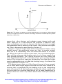
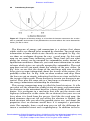
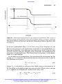
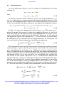
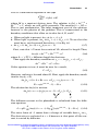
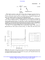
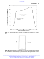
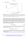
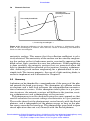
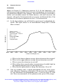
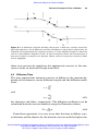
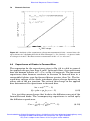
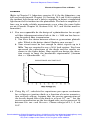
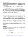
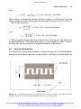
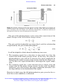
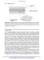
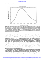
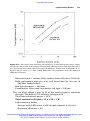
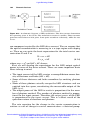
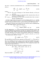
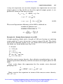
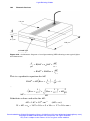
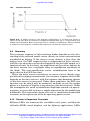
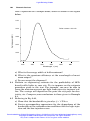
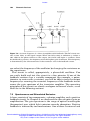
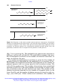
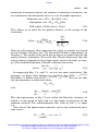
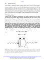
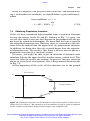
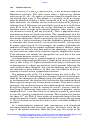
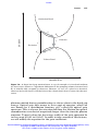
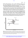
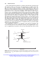
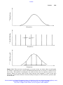
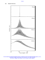
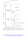
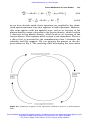
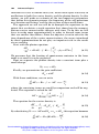
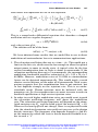
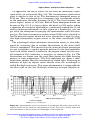
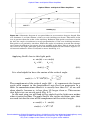
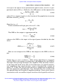
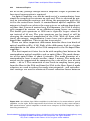
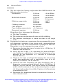
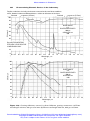
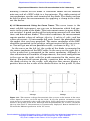
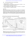
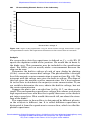
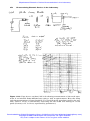
Electrical Response Time of Diodes Electrical Response Time of Diodes 4.4 65 Drift When the minority carrier reaches the depletion region (#2 and #4 in Fig. 4.1). Then it moves across the depletion region under the action of the electric field. The carrier velocity is proportional to the electric field until a velocity saturation is reached. The saturation electric field is about 3 × 10³ V/cm for common semiconductor materials such as GaAs, Ge, InGaAs, and Si. The electric field in the depletion region at 0 bias is much larger than the saturation field. This fact means that the carriers drift across the depletion region at constant velocity regardless of the reverse bias voltage. For electrons in Si, this is about 107 cm/sec, whereas for GaAs and InGaAs it is about a factor of two larger. The saturation velocity for holes in all semiconductors is about 106 cm/sec. The typical value for the depletion width is 1 m = 10–4 cm. Therefore, the drift time for carriers to cross the depletion region of this size is a few tens of picoseconds for either electrons or holes in all photodiode materials. Unlike the diffusion time, the drift time is linearly dependent on the drift distance. This feature can be used to improve the response time of indirect band gap photodiodes (i.e., Si or Ge) by replacing diffusion current with drift current. This will be discussed in more detail shortly. If we refer to the example above, the effect of replacing all the diffusion by drift current would shorten the intrinsic response time from 2 × 10⁻⁶ sec to 5 × 10⁻⁹ sec. If the diode were built on a p-type substrate, then electrons would be the minority carriers. A drift-dominated response time would be closer to 10–9 sec. To summarize so far, the response time for diffusion depends on the carrier mobility and the diffusion length. It does not depend on the size of the diode or on the bias voltage. The diffusion time can be quite short in photodiodes made from materials in which electrons or holes have very high mobility. For example, in Fig. 42, we show the time response of an InGaAs photodiode in which electrons have a mobility of about 10,000 cm2-V–1 sec–1, a factor of 10 greater than that for electrons in silicon. The response time due to drift current depends on the thickness of the depletion region and on the saturated drift velocity. The saturated drift velocity is approximately one order of magnitude higher for electrons than for holes. The velocity is independent of the electric field. The response time due to drift current does not depend on the size of the diode, but it can depend on the bias voltage, because an increase in the bias voltage will make the depletion region wider. The speed of transport by diffusion cannot be compared directly to the speed of transport by drift current, since these two mechanisms do not have the same dependence on distance. Downloaded from Digital Engineering Library @ McGraw-Hill (www.digitalengineeringlibrary.com) Copyright © 2004 The McGraw-Hill Companies. All rights reserved. Any use is subject to the Terms of Use as given at the website.