1
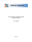
ENDCAP Alignment
CMS CCD OPTICAL POSITION SENSOR
READOUT BOARD
User’s Manual
FNAL – PNPI
2003
COPS Readout Board
User’s manual
Contents
1. Introduction
3
2. Construction
3
3. Circuit Diagram
4
4. Application Notes
9
5. Functioning
9
6. CPLD Programming
14
7. Flash Memory Programming
16
8. Debugging and Testing
19
9. Troubleshooting and Maintenance
26
10. Specification
30
Appendix 1. Command Description
32
Appendix 2. CPLD Firmware Description
39
Appendix 3. Brief List of Commands
43
Page 2 of 43
COPS Readout Board
User’s manual
1. Introduction
The readout board provides the CCD optical position sensor (COPS) with two voltages
and three clock signals, receives analog data from it, converts data to a digital form,
processes digital data to decrease information flow (DCOPS), and transfers requested
digital data to a host computer. It provides a measurement of the board temperature also.
The readout board has two programmed components (Xilinx CPLD and Atmel flash
memory) that must be programmed before using it. The CPLD is mounted to the printed
circuit board; it can be programmed through the input connector P2. The flash memory
must be programmed externally and then inserted into the socket.
The readout board has its own unique number (address) defined by set of eight shunts at
SW1 8x2 pin strip. This number must be set before using.
Data exchange is performed using serial protocol 8N1 (8 bits, Non-parity, 1 stop bit) with
LVDS levels at 115,200 bps baud rate. Baud rate is fixed and cannot be changed.
The readout board is ready to use after turning of a power. No action is performed until a
command is received; the readout board is always in a state of waiting for commands.
2. Construction
The readout board is printed-circuit board assembled with all its surface mount
components apart from flash memory AT29LV010A. The flash memory chip is inserted
into a socket after its programming. There are three 3M 10x2 headers (connectors) on the
board:
P1 – for connection with COPS, marked as “SENSOR”,
P2 – input data exchange connector (upstream), marked as “IN”,
P3 – output data exchange connector (downstream), marked as “OUT”.
The readout board has a 2 x 8 pin strip marked as SW1 BOARD NUMBER with eight
shunts. It is used to set the unique board number. Non-used shunts should be set to a
single pin.
Hardware reset is available. Press-button SW2 marked as RESET is arranged on the
printed circuit board. Power cycling also provides a reset and initialize.
Page 3 of 43
COPS Readout Board
User’s manual
3. Circuit Diagram
The readout board consists of the following basic parts (see Fig. 1):
◊ Front-end electronics (FE)
◊ Analog-to-Digital Converter (ADC)
◊ Level converter circuits (not shown)
◊ Timer
◊ Digital signal processor (DSP)
◊ Universal asynchronous receiver/transmitter (UART)
◊ LVDS interface
◊ DC-DC converters
Front-end electronics (FE) (see scheme, page 1) performs the function of correlated
double sampling (CDS) of input signals. It includes the analog switches 74HC4066 (U1,
U2), followers AD823 (U3 – U6), operational amplifiers OP463 (U8A – U8D), a voltage
reference LM4041 (V1) and a digital-to-analog converter (DAC) LTC1451 (U7) used to
correct pedestal.
The analog switches U1, U2 are controlled by two signals BASE5V and PEAK5V
produced by the timer and converted to a high voltage level by U29.
The DAC is loaded by the DSP through a 3-wire serial port: DACS5V provides the DAC
chip select and DACD5V presents serial DAC data in. The general periphery clock
SCLK5V is used for synchronization of the DAC, ADC and serial ports of DSP. It is
provided by the timer. All signals need to be level converted between 3.3V and 5V logic.
The default value loaded to DAC during initialization is 0.
The front-end electronics (FE) is powered by a +5V DC-DC converter that is switched
on during a conversion only.
Analog-to-Digital Converter (ADC) (U9, see scheme, page 1) converts four analog
input signals into digital form using +4.096V (V2) as a reference voltage. The ADC is
controlled by DSP through a 4-wire serial port: ADCS5V provides ADC chip select,
ADCD5V presents serial ADC data in used for conversion control, ADCO5V presents
ADC data output as a result of conversion. The general periphery clock SCLK5V
provided by the timer is used for synchronization of the DAC, ADC and serial ports of
DSP.
Apart from these, the ADC produces the ready flag signal ADCF5V to inform DSP about
its readiness to conversion. All signals need a conversion of level between 3.3V and 5V
logic.
The ADC is powered by a +5V DC-DC converter that is switched on during a conversion
only.
Page 4 of 43
+9 V
Front-end
DCOPS
READOUT BOARD
Sensor
connector
Page 5 of 43
+5 V
DC-DC
converters
Board
Number
Switch
Fig. 1. Structure of the DCOPS readout board
ADC
UART
DSP
Timer
(CPLD)
Power
Monitor
Flash
Memory
Temperature
Sensor
Downstream
connector
+3.3 V
LVDS
Interface
Upstream
connector
COPS Readout Board
User’s manual
+(10...15) V
COPS Readout Board
User’s manual
Level converter circuits (U21, U29, see scheme, page 3) convert 3.3V logic levels to 5V
levels for the DAC, ADC, analog switches, and CCD sensors. U22 is used for reverse
level conversion, as it is tolerant to 5V levels.
U21, U29 are powered by the +5V DC-DC converter that is switched on during a
conversion only. U22 is powered by a +3.3V DC-DC converter.
Timer (see scheme, page 3) is established in the Xilinx CPLD (U26). It produces the
general periphery clock SCLK by continuously dividing the input 20Mhz clock by 10.
Also it produces the control sequence 0CLK, 0RS, 0ROG for CCD sensors, BASE and
PEAK for correlated double sampling circuitry, 0ADCCS for analog-to-digital converter,
and start of conversion TF0 for DSP conditionally. The DSP produces a command
addressed to the timer as a periphery device with address 16 that enables this control
sequence to perform the reading of CCD sensor and conversion of received data. The
integrated circuit 74HCT365 (U29) converts these 3.3V level signals to 5V level.
In addition, the CPLD performs decoding of the DSP command to control the timer,
UART, and the board number gates. Any DSP command addressed to a periphery device
is defined by an input/output memory select signal IOMS, transfer direction 0RD (read)
or 0WR (write), and address A0…A4. The DSP uses higher addresses internally and for
operations with the flash memory. The timer operates with the single data bit D0 defining
start and prolongation of the sensor data conversion.
The DSP commands addressed to UART are converted by the CPLD to a chip select
signal 0PCIA and read or write signals 0PCIRD, 0PCIWR. The used address field of
UART is 0…7.
The CPLD converts the DSP periphery read command with address 18 to a 0RDADR
signal that enables gates U30 to read the board number switch SW1.
Finally, the CPLD inverts the interrupt request IRQA to 0IRQA for the DSP and the
active board flag ACTIVE to 0ACTIVE for the LVDS interface. In addition, the CPLD
produces a DSP reset signal uPRST caused by the hard reset signal PWRST or soft reset
DSP command with address 17.
Programming of the CPLD is performed through JTAG loop after PCB assembly. Four
signals are used for this purpose: TMS (Test Mode Select), TCK (Test Clock), TDI (Test
Data In), and TDO (Test Data Out). The TMS, TCK, and TDI signals come from the P2
input connector through the LVDS/CMOS interface. Also, TMS and TCK are translated
to the P3 output connector through the CMOS/LVDS interface for use by the next
readout boards. The TDI signal comes to the input of CPLD; the TDO signal goes from
the CPLD to the P3 output connector through the CMOS/LVDS interface and returns to
host through a reverse chain.
See details in the CPLD firmware description.
Page 6 of 43
COPS Readout Board
User’s manual
Digital signal processor (DSP) (U24, see scheme, page 3) performs general control and
data processing. It has a data bus (D0…D10) and an address bus (A0…A13) used for
data exchange with flash memory and the periphery devices: board number switch (SW1,
U30), UART (U28), and CPLD (U26). The DSP produces 0WR (Write) and 0RD (Read)
signals defining direction of data exchange and 0BMS, 0IOMS (Boot Memory Select and
I/O Memory Select respectively) signals to define the address field.
The DSP runs at double the crystal frequency; that is 20 MHz. The timer uses this output
clock signal also.
The DSP controls ADC and DAC through dedicated serial ports 0 and 1 respectively and
the level converters (U21, U22A, U22B). The digital thermometer (U20) is connected to
the DSP through a programmable serial port using I/O pins. The flash memory is
connected to the DSP through parallel data and address bus. Any operation with the flash
memory is accompanied by the boot memory select signal 0BMS. All other periphery
devices (timer, UART, the board number switch) are connected to the same data and
address bus; operation with them is accompanied by the input/output memory select
signal 0IOMS.
DSP commands addressed to the UART have the address field 0…7; they are converted
by the CPLD to 0PCIA, 0PCIRD, and 0PCIWR signals. The timer has address 16.
Address 17 is used by the CPLD to produce a soft reset of DSP. The DSP reads the board
number and loads it to the random access memory (RAM) during initialization caused by
the turning on power, hard or soft reset. To enable the gates U30 of the board number
switch SW1, the DSP produces the read command to the periphery device with address
18.
Programmable flags 9VRUN and 5VRUN are produced by the DSP to control the +5V
and +9V DC-DC converters. The DSP confirms its activity periodically by a HRTBT
signal that comes to the power monitor (U27). The power monitor produces a PWRST
(Power Reset) signal if it does not receive a HRTBT signal during certain time (about 1.2
s). The power monitor produces a PWRST signal on power-up or by pressing the reset
press-button (SW2). This signal initializes the UART and DSP. The DSP needs an
inverted reset signal; therefore, PWRST is inverted in the CPLD and comes into the DSP
as uPRST. Initialization of the DSP is a preset of its mode and loading of the program
code from the first page of flash memory to the random access memory (RAM) of DSP.
Universal asynchronous receiver/transmitter (UART) (U28, see scheme, page 3)
works under DSP control and provides data exchange between the DSP and host through
a LVDS interface. DSP commands addressed to UART are converted by the CPLD to the
chip select signal 0PCIA and read or write signals 0PCIRD, 0PCIWR. The used address
field of UART is 0…7. UART provides serial data transfer at 115,200 bps baud rate
using 8N1 format, that is 8 bits, Non-parity, 1 stop bit.
LVDS interface (see scheme, page 2) provides LVDS/CMOS and reverse level
conversion for received/transmitted data and JTAG signals. It includes LVDS receivers
Page 7 of 43
COPS Readout Board
User’s manual
(U10, U11, U15) and LVDS drivers (U12, U13, U14). Connector P2 is upstream, and
connector P3 is downstream.
Data from the host through U11A comes to the UART data input RX and U14A driver
also, so the same data exists at the downstream connector P3. Output data TX from the
UART comes to the P2 connector through the U16 gates and U12B driver if the current
board is active. Otherwise, data from the next board in a chain comes through the P3
connector, the U15B receiver, U16 gates, U12B driver to the upstream P2 connector and
further on to the host. The DSP selects a source of transmitted data by means of
0ACTIVE signal that controls the U16 gates.
JTAG signals include TMS (Test Mode Select), TCK (Test Clock), TDI (Test Data In),
and TDO (Test Data Out). The TMS, TCK, and TDI signals come from the P2 input
connector through U10A, U10B, and U11B, respectively, to the corresponding inputs of
the CPLD. Also, the TMS and TCK signals are translated to the P3 output connector
through U13A, U13B for use by the next readout board. The TDI signal comes to the
input of the CPLD; the TDO signal goes from the CPLD to the P3 output connector
through U14B forming a daisy chain of CPLDs arranged on different readout boards. The
last daisy-chained readout board returns the TDO signal to the host through a terminator
inserted into the P3 connector, U15A, U12A, P2, and previous readout boards.
DC-DC converters (see scheme, page 2) provide three voltages:
+3.3V to supply digital circuitry,
+5V to supply analog front-end, ADC, and CCD sensors,
+9V to supply CCD sensors only
They operate in the same scheme using the LTC1474 step-down converter (U17, U18,
U19). Using air core inductors permits them to work in a strong magnetic field. The
+3.3V converter is switched on always. The +5V and +9V converters have program
control from the DSP by means of 5VRUN and 9VRUN signals.
Page 8 of 43
COPS Readout Board
User’s manual
4. Application Notes
1. The readout board has three connectors used for both signal transmitting and power
connections. Therefore, it is very important to be sure that the power voltage is OFF
before connecting or disconnecting any cable.
2. Only one board can be active at a given time. Set the unique board number for each
board before it is included into the system. Binary code is used for the board number.
Non-used shunts should be placed on to a single pin as shown in Fig. 2.
Installed
shunts
SW1
Non-used
shunts
BOARD NUMBER:
7
6
5
4
3
2
1
0
Fig. 2. Sample of the board number setting (#19)
5. Functioning
The readout board is a passive device for a host. It performs commands and transfers data
as a response to commands from the host.
Each readout board has its unique board number, used as an address. The board number
is set by shunts at SW1. The permissible range of numbers is from 0 to 229. Numbers
230 to 255 are reserved for group operations. Installed shunt means logical “1” in the
corresponding binary bit. The board number 0 is used by firmware for testing and
debugging purposes only.
Host commands come through the serial LVDS inputs P2:13, P2:14, receiver U11A to
UART U28 and extends through the transmitter U14A and serial output P3:13, P3:14 to
the next readout board. The UART produces an IRQA interrupt signal (U28:30) which is
inverted by the CPLD U26 to 0IRQA. The DSP U24 receives the inverted interrupt
signal, reads the UART, decodes the received command, and performs it. All acceptable
commands can be separated into two groups: commands executed by DSP itself and
commands executed by the DSP with its periphery devices (timer, DAC, ADC, board
Page 9 of 43
COPS Readout Board
User’s manual
number switch). The UART as a periphery device is used by any command in both
receiving and response.
Commands listed below are executed inside of digital signal processor (DSP) including
flash memory.
CB
– Load the CCD background for calculations
CD
– Read CCD data from the DSP memory
CE
– Read the calculated meaning and RMS with subtracted background
CG
– Read CCD data with subtracted background from the DSP memory
CR
– Load the conversion repeat number
CS
– Read the calculated meaning and RMS
DD
– Display contents of the mentioned data memory location
DI
– Display contents of the mentioned IO memory location
DP
– Display contents of the mentioned program memory location
GD
– Display groups of the readout boards
GO
– Go to the mentioned memory location
GR
– Load default values for the groups
GS
– Load board numbers for the mentioned group
HE
– Display brief description of commands
LC
– Load the firmware code into the DSP program memory directly
OF
– Load the firmware code from the flash memory into the DSP internal
program memory
PC
– Display the board number and contents of the memory error counters
SC
– Test a checksum, display results for program, data, and flash memories
V5
– Load delay value (ms) between +5V switching on and start of
conversion
V9
– Load delay value (ms) between +9V and +5V DC-DC converters
switching on
VD
– Load default values of the switching on delays
WD – Write a value to the mentioned data memory location
WF
– Load the firmware code into the flash memory
WI
– Write a value to the mentioned IO memory location
WP
– Write a value to the mentioned program memory location
The following commands initiate execution with the board peripheral devices:
AP
– Turn On/Off +5V and +9V DC-DC converters
CC
– Start of the CCD data conversion
RT
– Reliability test
SD
– Load DAC
TT
– Read a temperature of the board
See Appendix 1 for full description of commands.
An execution of the above commands using peripheral devices must be considered more
carefully.
Page 10 of 43
COPS Readout Board
User’s manual
AP
– Turn On/Off +5V and +9V DC-DC converters
The DSP produces 5VRUN and 9VRUN signals in a certain sequence (see Fig. 3). These
continuous signals enable the corresponding DC-DC converters. A three second default
delay is necessary for proper functioning of the CCDs. It can be changed by V9 and VD
commands. Switching off occurs in the reverse order.
AP command
9VRUN
5VRUN
3 s (default)
Fig. 3. Sequence of turning on for +9V and +5V DC-DC converters
CC
– Start of the CCD data conversion
This command generates the most complicated execution:
1. The DSP switches on the +9V DC-DC converter.
2. After a delay defined as default or by the V9, VD commands the DSP switches on the
+5V DC-DC converter.
3. After a delay defined as default or by the V5, VD commands the DSP starts a series
of CCD conversions. This series consists of a number of flush cycles and one or
several useful data conversions. The flush cycle represents a data conversion cycle
when the DSP ignores any digital data produced by the ADC. The number of flush
cycles is equal to 10 as default and it can be changed by a parameter of the CC
command. The number of useful data conversions is defined by the CR command to
provide necessary statistic calculations. The default number is 1. Both delays are
necessary to set in the +9V and +5V voltages.
4. Each conversion cycle (both flush and useful) is executed by the timer synchronizing
a work of the CCDs, FE, ADC, and serial ports of the DSP. The DSP starts the
conversion cycle by means of addressing the timer (IOMS, address = 16, data = 0).
Four CCD sensors are examined in parallel; pixels are examined sequentially. The
timer established at the CPLD U26 completely defines the timing diagram of the
conversion as following.
• The addressed timer changes its internal state from Idle to Gate (see Appendix 2,
CPLD firmware) and produces the register output gate signal 0ROG to prepare
CCD sensors for reading. Then the timer changes its state to Scan.
Page 11 of 43
COPS Readout Board
•
User’s manual
The timer begins to produce a sequence of signals (see Fig. 4) controlling the
CCD sensors, correlated double sampling (CDS) circuitry, and ADC:
0RS
– Reset CCD sensor (ILX503A only),
0CLK – CCD clock,
BASE – Enable black level capture,
PEAK – Enable CCD data capture,
0ADCS – ADC chip select,
TF0
– Transfer flag starting the DSP operation with the ADC
Note. The system clock SCLK used by the ADC is produced by the timer continuously.
•
The timer sequentially examines 2087 pixels including 2048 real pixels and 39
dummy ones during the conversion cycle. The ADC converts the input data to a
digital form. The DSP reads the ADC output data and puts it into the data memory
of the DSP. In case of the flush cycle, the DSP ignores these data. Reading of the
last pixel returns the timer to the initial (Idle) state.
5. The DSP switches off the +5V DC-DC converter.
6. The DSP switches off +9V DC-DC converter
7. The captured data are processed by the DSP and can be read with CD or CS
commands from the data memory of the DSP.
SCLK
0
1
2
3 4
5
6
7
8
9
0
10 11 12 13 14 0
0RS
0CLK
BASE
PEAK
0ADCS
TF0
Fig. 4. Sequence of signals during the CCD data conversion
Page 12 of 43
COPS Readout Board
RT
User’s manual
– Reliability test
This command is intended for the test purposes only. On receiving the RT command, the
DSP switches on the +9V and +5V DC-DC converters once only, staying them in this
state. Then the DSP performs conversions like as for the CC command and displays two
lines of data. The first line contains means of four CCDs, the second one contains RMS
of four CCDs, the readout board number, the number of conversion, a count of reboots, a
count of the program memory errors, and a count of the flash memory errors. The RT
command is cycling until any key is pressed.
SD
– Load DAC
The DSP produces DACS (DAC Select) and DACD (DAC Data) signals to load the
mentioned value to the DAC. The SCLK signal (2 MHz) produced by the CPLD is used
for synchronization of both the DSP serial port and the DAC. These three signals come to
the DAC through the level converter U21.
TT
– Read a temperature of the board
The DSP reads the temperature sensor U20 through the 3-wire serial link. To control and
read the temperature sensor, the DSP produces the 0RST signal used as a frame, the clock
signal, and the control byte transferred as a data. The output data of the temperature
sensor are transmitted to the DSP using the same wire as the control byte.
Page 13 of 43
COPS Readout Board
User’s manual
6. CPLD Programming
Necessary equipment:
Computer running under Windows (9x, NT, 2000)
JTAG parallel download cable
Power cable for JTAG adapter
20-conductor ribbon cable for connection of the readout board to the interface
board
o 10 – 15 V power supply
o Digital voltmeter
o
o
o
o
Software to be used:
o XPLA PC-ISP Programmer 4.13 application
Warning:
Before programming of the CPLD, check +3.3V on the board.
Connect the JTAG download cable to the parallel port of a computer and to a power
supply. Connect an output connector of the JTAG download cable to the P2 connector of
the readout board, as shown in Fig. 5. Switch on a power and check presence of +3.3V
voltage on the readout board.
Run XPLA PC-ISP Programmer 4.04 application. Software must find out the download
cable and CPLD.
PC
Parallel Port Cable
Power Cable
Power
Supply
JTAG adapter
P2
Readout board
Terminator
Fig. 5. Programming of the CPLD
Page 14 of 43
COPS Readout Board
User’s manual
Fig. 6. XPLA PC-ISP Programmer window
Select the device name (XCR3064XL), operation (Program), and design file name
(Cops_New.jed), then press Execute button. Change operation to Verify and press
Execute button. In case of positive result, switch off power and disconnect the readout
board from the download cable.
Page 15 of 43
COPS Readout Board
User’s manual
7. Flash Memory Programming
Necessary equipment:
o Universal programmer “DATA I/O UNISITE” with its TaskLink software.
The code image file intended for the programming of the AT29LV010A flash memory
has *.bnm extension. To program the flash memory follow the next instructions:
1. Insert diskette #7 into the right (B) floppy drive of the DATA I/O UNISITE device.
2. Run the TaskLink application.
3. Select type of a chip to be programmed. For that sequentially select:
Setup > Select Device > ATMEL > 29LV010A-PLCC (see Fig. 7).
4. Select a source of data. For that sequentially select:
Data > Load RAM from PC/Network File.
Fig. 7. TaskLink. Select Device procedure
Page 16 of 43
COPS Readout Board
User’s manual
Fig. 8. TaskLink. Load RAM procedure
5. Enter the actual file name (a:\pcops-e.bnm) and select a translation format:
(82) Motorola EXORciser (see Fig. 8).
6. Select a mode:
Program > Program/Verify.
7. Select Process Devices.
8. Select OK in the Process Devices window (see Fig. 9).
9. Insert a chip and select the Start button (see Fig. 10).
Page 17 of 43
COPS Readout Board
User’s manual
Fig. 9. TaskLink. Process Devices procedure
Fig. 10. TaskLink. Program/Verify Start procedure
Page 18 of 43
COPS Readout Board
User’s manual
8. Debugging and Testing
Necessary equipment:
Computer running under Windows (9x, NT, 2000)
RS-232/RS-422 adapter
Interface board #1
Reference readout board
RS-232 serial link DB9/DB9 cable
RS-422 serial link RJ11/RJ11 cable
Power cable for RS-232/RS-422 adapter
Power cable for the interface board
Three 20-conductor ribbon cables for connection of the readout board to the
interface board, reference sensor, and reference readout board
o 10 – 15 V power supply
o Digital voltmeter
o
o
o
o
o
o
o
o
o
Software to be used:
o Hyper Terminal application
Properly manufactured readout boards do not require any adjustments. They should work
at once after programming of the CPLD and flash memory. This procedure is planned for
the worst case. If you have any problem, it is recommended to perform all operations
sequentially. The Quick-Fit male terminal P4 can be used as a ground pin during
measurements.
1. Check the assembled board visually. It must not have visible damages. All
components and their values must be in accordance with documents.
2. Program the CPLD as described in a chapter 6.
3. Program the flash memory chip AT29LV010A as described in a chapter 7. Turn off
power; insert the programmed flash memory chip into the socket on the board.
4. Set the board number; acceptable range is 1…229.
5. Connect the readout board under test to the interface board as shown in Fig. 11 and
switch on power. Check +3.3V output voltage of the corresponding DC-DC
converter. A test point marked as “3.3V” is arranged in area of the DC-DC converter.
6. Run Hyper Terminal application.
7. Select the serial port COM1 or another if COM1 port is occupied as shown in Fig. 12.
Page 19 of 43
COPS Readout Board
User’s manual
8. Press button “Configure…”
RS-232
RS-232/RS-422
Adapter
RS-422
PC
Interface
Board # 1
Adapter Power Cable
9. Select proper features as shown in Fig. 13:
115200 bps
8 bit
None parity
1 stop bit
None flow control
Power Cable
Power
Supply
P2
Reference
CCD
Sensor
P1
Readout Board Under Test
P3
P2
P1
Reference Readout Board
P3
Fig. 11. Diagram of connections
Page 20 of 43
COPS Readout Board
User’s manual
Fig. 12. Hyper Terminal. Select a serial port
10. Turn on power; input the board number followed by “Enter”. You should receive a
prompt containing the board number as a response. If response is not received, try
once more in the following sequence: “Enter”, the board number, “Enter” (you could
input illegal character). If response is not received again, see chapter 9.
11. Check execution of the TT command. Input the board number (12, for instance), TT,
“Enter”. As a response you should receive a current temperature in degrees of
centigrade:
<012> 12TT
<012> 24.6 C
Bolded characters belong to the input command; italic is used for a response of the
readout board. “Enter” is not shown.
If response is not received or it is wrong, see chapter 9.
Page 21 of 43
COPS Readout Board
User’s manual
Fig. 13. Hyper Terminal. Port settings
12. Check the LVDS interface at the downstream connector. Connect the reference
readout board to the downstream connector P3. Check execution of the TT command
for the reference readout board (with another board number).
If response is not received or it is wrong, see chapter 9.
Warning:
All reconnections must be performed with power turned OFF
13. Check the board number switch SW1. For that change the board number to 1, 2, 4, 8,
16, 32, 64, 128 (one shunt is set only), and 0. Perform this test in the following
sequence:
o Set the board number
o Press “Reset” button SW2
o Try the TT command with this board number
If any board number does not answer, see chapter 9.
Page 22 of 43
COPS Readout Board
User’s manual
14. Check execution of the CD command. As a response you should receive 2048 lines
containing data separated with semicolon:
<012> 12CD
0000;0000;0000;0000;
0001;0001;0001;0001;
0002;0002;0002;0002;
0003;0003;0003;0003;
…
081E;081E;081E;081E;
081F;081F;081F;081F;
0820;0820;0820;0820;
<012>
These data are written to the data memory during an initialization. Pay attention to
permanent length of lines.
If response is not received or it is wrong, see chapter 9.
15. It is not necessary to check all commands because their execution is provided by the
DSP firmware. Mentioned above tests check LVDS receivers and drivers, UART,
DSP, flash memory, and operation of the DSP with flash memory and periphery
devices (the temperature sensor).
Warning:
Do not use the following commands:
V5
V9
WI
WP
They are intended for an investigation only. Wrong use of these
commands can break a proper work of the board. To restore an initial
code perform one of the following actions:
− Enter OF command,
− Press the Reset button on the board,
− Perform cycling of power.
Warning:
Using of the LC command with a wrong code file can break a proper
work of the board. To restore an initial code perform one of the
following actions:
− Enter OF command,
− Press the Reset button on the board,
− Perform cycling of power.
Warning:
Using of the WF command with a wrong code file can break a proper
work of the board. To restore an initial code perform one of the
following actions:
− Use the WF command with the proper code file,
− Reprogram the flash memory (see chapter 7).
Page 23 of 43
COPS Readout Board
User’s manual
16. Check a power control. Input command AP with parameter 1 (turn on):
CC
– Start of the CCD data conversion
This command has a delay of execution about 3 seconds. Check voltages at the test
points marked as “+9V” and “+5V” by means of a digital voltmeter. The voltages
must be equal to the mentioned values with 5% tolerance. Turn off DC-DC
converters:
<012> 12AP 0
Analog power is OFF
<012>
If the DC-DC converters cannot be turned on by AP command or their output
voltages are wrong, see chapter 9.
17. Check a load of the DAC. The DAC is set to 0 as default during an initialization.
Load various values to the DAC (U7) and check its output voltage at the pin 7:
<012> 12SD 1000
DAC is set to 1000 - output voltage must be 1.00 V
<012> 12SD 2000
DAC is set to 1000 - output voltage must be 2.00 V
<012> 12SD 4000
DAC is set to 1000 - output voltage must be 4.00 V
<012> 12SD 0
DAC is set to 1000 - output voltage must be 0 V
<012>
If the DAC output voltage does not change, see chapter 9.
18. Check the CCD data conversion. Input command CC:
<012> 12CC
Flushes: 10 Repeats (exp2/val): 0/1
<012>
Time of execution is about 3 seconds. Check data received during a conversion:
<012> 12CD
000A;0009;000B;0010;
000A;0009;000B;0010;
000B;0009;000B;0010;
000A;0009;000B;0010;
…
081A;0010;000B;000F;
081A;0009;000B;0010;
082A;0009;000B;0010;
<012>
Pay attention to data values. Data received with disconnected CCD sensor must not
exceed 20 hexadecimal.
If data are wrong, see chapter 9.
Page 24 of 43
COPS Readout Board
User’s manual
19. Complete test of the readout board with the reference sensor. Turn off power.
Connect the reference CCD sensor to the connector P1 and turn on power. Execute
CC and then CD commands:
<012> 12CC
Flushes: 10 Repeats (exp2/val): 0/1
<012> 12CD
0060;006A;0070;0100;
0062;006A;006F;0100;
0061;006B;006F;00FF;
0062;006A;0070;0100;
…
0060;006B;0070;0100;
0061;006A;006F;0101;
0060;006A;006E;0100;
<012>
Data of each sensor have a peak. If you cannot discover these peaks, process the
received data with Excel or similar application.
If data are wrong, see chapter 9.
This is a complete set of tests to find any malfunction of the DCOPS readout board. The
board fulfils requirements if all results are positive.
Page 25 of 43
COPS Readout Board
User’s manual
9. Troubleshooting and Maintenance
Necessary equipment:
o Computer running under Windows (9x, NT, 2000)
o RS-232/RS-422 adapter
o Interface board #1
o RS-232 serial link DB9/DB9 cable
o RS-422 serial link RJ11/RJ11 cable
o Power cable for RS-232/RS-422 adapter
o Power cable for the interface board
o 20-conductor ribbon cable for connection of the readout board to the interface
board
o 20-conductor ribbon cable for connection of the reference sensor to the readout
board
o 10 – 15 V power supply
o Digital voltmeter
o Oscilloscope
Software to be used:
o Hyper Terminal application
Check a readout board in an order mentioned in chapter 8, then follow to the next
recommendations.
Warning:
All reconnections must be performed with power turned OFF
1. Output voltage of the +3.3V DC-DC converter is wrong.
•
•
•
•
•
•
Check an input voltage; it must be 10 to 15 V.
Check soldering points.
Check values of the R45 and R46 resistors.
Check polarity of the V3 diode (a silver band marks a negative pad).
Check polarity of the C11 and C17 tantalum capacitors (a white band marks a
positive pad).
If the previous checks do not discover a reason of failure, replace the U17
LTC1474 integrated circuit.
2. Output voltage of the +5V or +9V DC-DC converter is wrong.
•
•
•
•
Check a communication between the readout board and a host by the TT
command; if a communication failed, begin with points 3 and 4 of this
chapter.
Input the AP 1 command. (Do not forget the leading board number).
Check the 9VRUN and 5VRUN signals at pin 8 of U18, U19; they must be
high.
If the 9VRUN and 5VRUN signals are high, perform actions listed in point 1
of this chapter.
Page 26 of 43
COPS Readout Board
•
•
•
User’s manual
If the 9VRUN and 5VRUN signals are low, check these signals at outputs of
DSP (pins 86 and 85 respectively).
If the 9VRUN and 5VRUN signals are high at outputs of DSP, restore a
damaged conductor.
If the 9VRUN and 5VRUN signals are low at outputs of DSP, reprogram the
flash memory.
3. There is no response (prompt) to the entered board number.
•
•
•
•
•
•
•
•
Connect the reference readout board to the downstream connector P3.
Set the reference board number to 0, press the Reset button. The readout
board produces the continuous prompt until any key pressed.
Input the 0TT command for the reference readout board. If there is no
response from it, the LVDS interface circuitry of the board under test is
invalid. Check the following path:
o U15 pins 3, 4, 6
o U16 pins 12, 11, 10, 8
o A high level must be at the U16 pin 13; it is determined by the
0ACTIVE signal produced by the DSP. If 0ACTIVE is low, check the
shortened conductors and then reprogram the flash memory. The last
action is the replacing of the DSP.
o U12 pins 3, 6, 5
o Replace found invalid components.
If there is a proper response from the reference readout board, the LVDS
interface circuitry of the board under test is valid. Then it is necessary to
check the DSP, CPLD and UART.
Disconnect the reference readout board from the downstream connector P3.
Set the board under test number to 0, press the Reset button. The readout
board produces the continuous prompt until any key pressed.
Using an oscilloscope, check oscillators of the DSP and UART.
Check a presence of output signals in the following path:
o U24 pins 19, 20, 24 (0WR, 0RD, 0IOMS respectively). If there are no
signals, make sure that there is no shortened conductors, then
reprogram the flash memory. In case of the same result after
reprogramming memory, replace the DSP.
o U24 pins 97, 98, 99, 100, 1 are used to address the UART (A0…A4).
o U24 pins 13 - 15, 17 - 21 are used for data exchange (D0…D7).
o Check a presence of the 0WR, 0RD, 0IOMS, and A0…A4 at inputs of
the CPLD U26 (pins 38, 39, 44, 3, 5, 6, 8, 10 respectively).
o The CPLD decodes these signals and produces 0PCIWR, 0PCIRD,
0PCIA (pins 28, 25, 27) to control the UART. If there are no signals,
make sure that there is no shortened conductors, then reprogram the
CPLD.
o The UART receives 0PCIWR, 0PCIRD, 0PCIA (pins 15, 19, 10) from
the CPLD, address A0…A2 and data directly from the DSP. Check
these signals at inputs of the UART.
Page 27 of 43
COPS Readout Board
•
•
•
•
•
•
•
•
•
User’s manual
o Check the output signal TX of the UART. If all input signals of the
UART are valid, and there is no TX, replace the UART.
In case of presence the TX signal, check the LVDS interface circuitry
following TX:
o U16B pins 5, 6, 9, 8. A high level must be at the pin 4; it is determined
by the 0ACTIVE signal produced by the DSP and inverted by U16A.
If 0ACTIVE is high:
Check the shortened conductors.
Check an absence of the PWRST signal at the power monitor
U27 output; it must be low. If PWRST is high, check for:
Shortened conductors,
Latched up SW2 press-button,
Presence of the HRTBT signal confirming an activity of
the DSP.
Reprogram the flash memory.
Replace the DSP.
o Follow TX further: U12 pins 3, 6, 5.
Eliminate defects and try the 0TT command once more. If there is no
response follow the next instructions.
Set the board number to 1, press the Reset button.
Press and hold key 1 on a keyboard. You can use any enough heavy object for
this purpose to have hands free.
Using an oscilloscope, check a presence of an input signal at pins 1 and 2 of
the U11A receiver. Take a synchronization of oscilloscope from the pin 2.
Using another probe, check an input signal path:
o U11A pin 7
o U14A pin 2
o U14A pins 7, 8
o U28 pin 5
The UART U28 must produce an interrupt signal IRQA; follow it:
o U28 pin 30
o U26 pin 15
o U26 pin 43
o U24 pin 26
The DSP U24 must read data from the UART and send an echo to it:
o U24 pins 20, 19, 24
o U26 pins 39, 38, 44
o U26 pins 25, 28, 27
o U28 pins 19, 15, 10
Address bits A0…A4 are used for decoding of the DSP command also. Data
exchange between the UART and DSP occurs through the data bus D0…D7.
Replace the found failed component. If the found failed part is the CPLD U26,
reprogram it.
Restore the initial board number.
Page 28 of 43
COPS Readout Board
User’s manual
4. Response to the entered TT or CD commands has a distortion.
Check a configuration of the serial port used for communication.
Check the used serial port with the reference readout board.
Check all cable connections.
If all external staff is valid, follow point 3 of this chapter.
5. Operation with some board numbers has no response; other board numbers are
valid.
Find shortened conductor or component and eliminate defect.
6. The DAC cannot be loaded.
Input the AP 1 command (+9V and +5V turning on).
Input command SD 1000 1 (loading of the DAC in loop).
Check communication of the DAC and DSP with oscilloscope.
Eliminate found defects.
7. Data received with disconnected CCD sensor exceed 20 hexadecimal.
Check output voltage of the DAC; it must be zero. Otherwise, see point 6 of
this chapter.
Check values of all resistors in the front-end circuitry.
Input command CC 3 1 (CCD data conversion in loop).
Check +9V and +5V voltages; they must be turn on before a conversion and
turn off after it.
Check all output signals produced by the timer to control the CCD sensor
(0RS, 0ROG, 0CLK), the front-end (BASE, PEAK), the ADC (SCLK, ADCS,
ADCD), and their timing. Follow these signals from the timer CPLD to
targets.
Check communication between the ADC and DSP.
Eliminate found defects and check the readout board once more.
8. Data received with the connected reference sensor has no peak
Check a cable connection between the CCD sensor and the readout board.
Follow the CCD sensor output signals from the sensor connector P1 to the
ADC.
Eliminate found defects and check the readout board once more.
Page 29 of 43
COPS Readout Board
User’s manual
10. Specification
General
Dimensions of the board
Sensor connector P1
Input connector P2
Output connector P3
Board number switch SW1
Board number format
Board number range
Warning:
6.7” x 2.9”
10 x 2 header 3M 3428-6002
10 x 2 header 3M 3428-6002
10 x 2 header 3M 3428-6002
8 x 2 double raw strip
3M 929665-09-36-I (modified)
with shunts 3M 929957-08
binary
1…229
The board number must be set before mounting of the readout board to its
proper place.
Power characteristics
Minimum input voltage
+10 V
Maximum input voltage
+15 V
Power consumption:
Idle mode
300 mW
Conversion mode without sensor
355 mW
Conversion mode with connected sensor 725 mW
Current consumption:
Idle mode
30 mA @ 10.0 V
21 mA @ 14.2 V
20 mA @ 15.0 V
Conversion mode without sensor
36 mA @ 10.0 V
25 mA @ 14.2 V
24 mA @ 15.0 V
Conversion mode with connected sensor 73 mA @ 10.0 V
51 mA @ 14.2 V
48 mA @ 15.0 V
On board power protection:
Fuse
0.5 A
Each DC-DC converter limits its output current
Output current threshold
0.4 A
Communication features
Protocol
Transfer format
Signal levels
Baud rate
Termination
asynchronous serial
8N1 (8 bits, Non-parity, 1 stop bit)
LVDS
115,200 bps
118 Ohm
Page 30 of 43
COPS Readout Board
User’s manual
Specification of connectors
Sensor connector P1:
Name
+5V output
GND
GND
GND
GND
GND
0ROG5V output
0CLK5V output
0RS5V output
+9V output
Pin
1
3
5
7
9
11
13
15
17
19
Pin
2
4
6
8
10
12
14
16
18
20
Name
+5V output
CCD1 input
CCD2 input
CCD3 input
CCD4 input
Pin
1
3
5
7
9
11
13
15
17
19
Pin
2
4
6
8
10
12
14
16
18
20
Name
TCK- input
TDO- output
TMS- input
GND
TDI- input
GND
RX- input
TX- output
GND
+12V input
Pin
1
3
5
7
9
11
13
15
17
19
Pin
2
4
6
8
10
12
14
16
18
20
Name
TCK- output
TDO- input
TMS- output
GND
TDI- output
GND
TX- output
RX- input
GND
+12V output
GND
GND
GND
GND
+9V output
Input connector P2:
Name
TCK+ input
TDO+ output
TMS+ input
Non used
TDI+ input
GND
RX+ input
TX+ output
GND
+12V input
Output connector P3:
Name
TCK+ output
TDO+ input
TMS+ output
Non used
TDI+ output
GND
TX+ output
RX+ input
GND
+12V output
Warning:
The 20-contact terminator must be installed into the output connector P3
if this board is last in a chain.
Page 31 of 43
COPS Readout Board
User’s manual
Appendix 1. Command Description
Command Format
Format of any command for the readout board is the following:
ddd [ NM [p1 [p2]] ]
Where:
ddd
NM
p1, p2 ...
- the decimal board number in a range of 0 to 255
(leading zeros can be omitted),
- an abbreviation of the command name (two letters),
- admissible command parameters (can be omitted).
Any command must begin with a decimal board number.
A decimal card number is omitted in a description of commands; but it is implied.
Parameters in square brackets can be omitted.
Warning:
Absence of the prompt and echo is possible in the following cases:
The first character is not a decimal digit. Press ENTER and begin
a new command with a digit.
The mentioned board number does not exist. Press ENTER and
input an existing board number.
The board number can represent a unique board number or group number assigned to
some range of board numbers. A group number allows simultaneous execution of a
current command by all boards included into the mentioned range of numbers.
The latest command containing an individual board number makes this board active. The
active board produces both a prompt and an echo. A prompt is the decimal board number
enclosed in angle brackets <ddd>. A group command does not affect to the active board
number.
Numbers 0 to 229 are allocated for physical boards. The board number 0 is dedicated for
a debugging purpose only. On power-up or reset, the board with number 0 becomes
active and produces a continuous prompt until any key pressed. Numbers 230 to 255 are
allocated for group numbers. By default, the following ranges of numbers are assigned to
group numbers:
Group
230
231
…
251
252
Board number range
0-9
10 - 19
…
210 - 219
220 - 229
Page 32 of 43
COPS Readout Board
User’s manual
253
0 - 229
254
0 - 229
255
0 - 229
A group range can be reassigned by the GS command, except for the group 255.
Basic Commands
HE
– Transfer a brief description of commands
CC [N [L]]
– Execute the CCD data conversion, put the received data into the memory
N is a decimal number defining number of CCD flush cycles; default N is
equal to 10.
Data are sampled RN (Repeat Number) times; sum and average values are
calculated for each pixel. The repeat number RN is defined by the CR
command:
RN = 2E.
L is any decimal number except for zero. It defines a continuous execution
of the command for a debugging purpose. L = 0 does not affect to an
execution.
CR E
– Set the conversion repeat number RN
E is an exponent of 2 (0, 1, 2, 3) that corresponds to numbers 1, 2, 4, 8.
The CR command defines the repeat number (RN) of the CCD data
samples during execution of the CC command to calculate sum and
average values for each pixel:
RN = 2E.
CD [N]
– Transfer CCD data from the DSP memory
Output data are hexadecimal; each line contains data of four CCDs in
ADC counts.
N defines a kind of statistic calculation:
N = 1: a sum of values for each pixel (see CC and CR commands);
N = 2: an average value for each pixel with subtracted an average value
for all pixels;
N = 3: a sum of values for each pixel with subtracted an average value
for all pixels;
N is omitted or equal to any other decimal number: an average value for
each pixel.
Page 33 of 43
COPS Readout Board
CS [N]
User’s manual
– Transfer the CCD data statistics values, that is mean and RMS
The first lines contains means of four CCDs in pixels, the second line
contains RMS in pixels (decimal numbers).
N defines a kind of statistic calculation:
N = 1: a sum of values for each pixel (see CC and CR commands);
N = 2: an average value for each pixel with subtracted an average value
for all pixels;
N = 3: a sum of values for each pixel with subtracted an average value
for all pixels;
N is omitted or equal to any other decimal number: an average value for
each pixel.
CG [N]
– Transfer CCD data with the subtracted background value
If the background is set to zero by the CB command, result is the same as
for a CD command. Output data are hexadecimal; each line contains data
of four CCDs in ADC counts.
N defines a kind of statistic calculation:
N = 1: a sum of values for each pixel (see CC and CR);
N = 2: an average value for each pixel with subtracted an average value
for all pixels;
N = 3: a sum of values for each pixel with subtracted an average value
for all pixels;
N is omitted or equal to any other decimal number: an average value for
each pixel.
CE [N]
– Transfer the CCD data statistics values, that is mean and RMS, with the
subtracted background value
If the background is set to zero by the CB command, result is the same as
for a CS command. The first lines contains means of four CCDs in pixels,
the second line contains RMS in pixels (decimal numbers).
N defines a kind of statistic calculation:
N = 1: a sum of values for each pixel (see CC and CR commands);
N = 2: an average value for each pixel with subtracted an average value
for all pixels;
N = 3: a sum of values for each pixel with subtracted an average value
for all pixels;
N is omitted or equal to any other decimal number: an average value for
each pixel.
Page 34 of 43
COPS Readout Board
CB [N]
User’s manual
– Set the CCD background value
This background value is used by CG and CE commands.
N is the decimal number defining a background value used by the CG and
CE commands. If N is specified, it defines the background value as N for
an average calculation and as N*RN for a sum calculation, where RN is a
repeat number parameter of the CG or CE command. If N is omitted, the
background value is defined by the average and sum calculated from the
latest CCD data.
The default background value is zero.
TT [L]
– Capture and transfer a current temperature of the readout board in
degrees of centigrade.
L is any decimal number except for zero. It defines a continuous execution
of the command for a debugging purpose. L = 0 does not affect to an
execution.
GR
– Set the board number ranges for all groups to the default values:
Group
230
231
…
251
252
253
254
255
Board number range
0-9
10 - 19
…
210 - 219
220 - 229
0 - 229
0 - 229
0 - 229
GD [M [N]] – Transfer the board number range for groups M to N
If N is omitted, information about the group M is transferred; if both
parameters are omitted, all groups are transferred. The group containing
the active board is marked by asterisk.
GS G M N
– Assign the boards with numbers M to N to the group number G.
The group number 255 cannot be changed.
Page 35 of 43
COPS Readout Board
SD [D [L]]
User’s manual
– Set the DAC offset value to the decimal number D
Acceptable range of D is 0 to 4095; its value will be truncated to 4095, if
D > 4095. The default offset value is zero. If both parameters are omitted,
the board transfers a current offset value.
This code will be loaded into the DAC in the following cases:
o By CC command
o By AP command, with the nonzero first and second parameters
o By this command, if +9V, +5V power is turned on (by the AP
command) and if L > 0 is entered. In this case the loading of the
DAC is looped with L (ms) interval until any key pressed
PC
– Transfer the board number and contents of the reboot counter, DSP
program memory error counter, and flash memory error counter
MC
– Test checksums of the DSP program memory, DSP data memory, and
flash memory; transfer results.
OF PP
– Load the firmware code from the flash memory (page PP) into the DSP
program memory
PP is a hexadecimal number.
WF PP
– Load the firmware code into the flash memory (page PP)
The board waits for loading of Motorola S-file.
PP is a hexadecimal number.
Maintenance Commands
AP [N [D]]
– Turn on/off +9V and +5V DC-DC converters
D is a decimal number defining the DAC offset value
N is a decimal number defining on/off and debugging modes:
N = 0 - turn off +9V and +5V DC-DC converters
N > 0 - turn on +9V and +5V DC-DC converters if they are turned off
N = 0 - turn off +9V and +5V DC-DC converters
N > 0 and D > 0 - turn on +9V and +5V DC-DC converters and load the
DAC with the D offset value after voltages set in.
N = 99, D > 0 and +9V, +5V DC-DC are turned off turning on the DC-DC converters, loading of the DAC with the D
offset value, and turning off the converters are looped until any key
pressed
Page 36 of 43
COPS Readout Board
User’s manual
The board transfers current state of DC-DC converters in a case of AP
command without parameters.
During an execution of the CC command, +9V and +5V DC-DC
converters are switched on at the beginning and switched off at the end of
conversion by the DSP; no external command is required.
RT [N [D]]
– Reliability test
+9V and +5V DC-DC converters are turned on permanently. The DSP
performs the CCD data conversion, processing of the received data,
transfer means, RMS (for each CCD), the board number, contents of the
reboot counter, DSP program memory error counter, and flash memory
error counter in cycle until any key pressed.
Commands for Research Purpose
V9 [D [S]]
– Set the delay value after the +9V turning on
D is a decimal number defining the delay value.
S > 0 defines an order of turning on DC-DC converters as +9V then +5V.
Turning off occurs in a reverse order.
The board transfers current settings in a case of V9 command without
parameters.
V5 [D [S]]
– Set the delay value after the +5V turning on
D is a decimal number defining the delay value.
S > 0 defines an order of turning on DC-DC converters as +5V then +9V.
Turning off occurs in a reverse order.
The board transfers current settings in a case of V9 command without
parameters.
VD
– Restore the default delay values and an order of turning on DC-DC
converters as +9V then +5V.
Turning off occurs in a reverse order.
The default delay after the +9V turning on is 100 ms.
The default delay after the +5V turning on is 3 s.
Page 37 of 43
COPS Readout Board
DD aaaa bbbb
User’s manual
– Transfer a contents of data memory locations aaaa to bbbb
Parameters must be hexadecimal numbers.
If bbbb is omitted, the board transfers a contents of the location
aaaa only.
WD aaaa dddd [[eeee] …] – Write 16-bit data word(s) dddd, [eeee] and so on to the
data memory locations starting from the address aaaa
Parameters must be hexadecimal numbers.
DI aaaa bbbb – Transfer a contents of I/O memory locations aaaa to bbbb
Parameters must be hexadecimal numbers.
If nnnn is omitted, the board transfers a contents of the location
mmmm only.
WI aaaa dddd
– Write 16-bit data word dddd to the I/O memory location aaaa
Parameters must be hexadecimal numbers.
DP aaaa bbbb
– Transfer a contents of program memory locations aaaa to bbbb
Parameters must be hexadecimal numbers.
If bbbb is omitted, the board transfers a contents of the location
aaaa only.
WP aaaa dddddd [[eeeeee] …]
– Write 24-bit instruction word(s) dddddd, [eeeeee]
and so on to the program memory locations
starting from the address aaaa
Parameters must be hexadecimal numbers.
GO aaaa
– Jump to the memory location aaaa
Parameter must be a hexadecimal number.
LC
– Load the firmware code directly into the DSP program memory
The board waits for loading of Motorola S-file.
Page 38 of 43
COPS Readout Board
User’s manual
Appendix 2. CPLD Firmware Description
This firmware is written using Xilinx hardware description language (HDL), compiled
with Xilinx WebPack, and prepared to be downloaded with XPLA PC-ISP Programmer.
module Cops_New;
title 'COPS timebase generator for CCD, CDS. DSP address decoder.
Sten Hansen
Fermilab
06-06-01'
"
Modified 7-31-98 for use with second version of board S.H.
"
Added inversion for UARTB IRQ line.
"
Corrected CSADC clocking for 20 MHz clock
"
Added status bit to check state of conversion sequencer
"
Updated to layout as of 12-15-99
"
Changed timing to accommodate new UART
"
* Modified 3-29-00 by Vladimir Sknar
"
*** Modified 6-06-01 for use with the third version of board S.H.
"
*** Pin assignment is changed to correspond to the new layout
" Inputs
CLK20, PWRST
nWR, nRD, nIOMS
D0
A0..A4
TXENB, IRQA
" Outputs
nCLK, nRS, nROG
BASE, PEAK
SCLK, nADCCS, TF0
nPCIRD, nPCIWRT
nPCIA, nIRQA, nPRST
RDADR, nRDADR, nTXENB
UDly1, UDly0
Q3..Q0
PS2, PS1, PS0
R1, R0
DL1, DL0
pin 37,31;
pin 38,39,44;
pin 2
istype 'buffer';
pin 3,5,6,8,10;
pin 14,15;
pin 18,19,20
pin 21,22
pin 35,23,42
pin 25,28
pin 27,43,34
pin 30, 33,13
istype 'reg_T';
istype 'reg_T';
istype 'reg_T';
istype 'reg';
istype 'buffer';
istype 'buffer';
node
node
node
node
node
istype 'reg';
istype 'reg';
istype 'reg';
istype 'reg';
istype 'reg_T';
H,L,C,X = 1,0,.C.,.X.;
Page 39 of 43
COPS Readout Board
User’s manual
" Define State Machine states..
Run = [R1,R0];
Idle
= [ 0,0 ];
Gate = [ 0,1 ];
Scan = [ 1,1 ];
Finish = [ 1,0 ];
Udly
Didle
Wait1
Wait2
Wait3
= [UDly1,UDly0];
= [ 0 , 0 ];
= [ 0 , 1 ];
= [ 1 , 1 ];
= [ 1 , 0 ];
" Group signals into sets..
Addr = [A4..A0];
PS
= [PS2..PS0];
Count = [Q3..Q0];
Timing = [BASE, PEAK, nRS, nCLK];
DLROG = [DL1,DL0];
Equations
" Registers Clock and Preset
[Count.C, Timing.C, nADCCS.C, nPCIRD.C, nPCIWRT.C]
[Run.C, UDly.C, PS.C, SCLK.C, TF0.C, nROG.C, DLROG.C]
= CLK20;
= CLK20;
[Count.AP, Timing.AP, nADCCS.AP, nPCIRD.AP, nPCIWRT.AP] = PWRST;
[Run.AR, UDly.AR, PS.AR, SCLK.AR, TF0.AR]
= PWRST;
nROG.AP = PWRST # (Run != Gate);
DLROG.AR = PWRST # (Run != Gate);
" D0=1 from DSP: Enable Idle -> Gate transition
" D0=0 from DSP: Enable Scan -> Finish transition
" D0 = 1 is selfholding in all states excepting Idle
D0.oe = !nIOMS & !nRD & (Addr == ^h10);
D0
= !(Run == Idle);
" Select lines for UART chip
!nIRQA
= IRQA;
!nPCIA
= !nIOMS & (Addr < ^h8);
!nPCIWRT := (!nPCIA # (UDly != DIdle)) & !nWR;
!nPCIRD := (!nPCIA # (UDly != DIdle)) & !nRD;
" DSP reset line
!nPRST = PWRST # !nIOMS & !nWR & (Addr == ^h11);
Page 40 of 43
COPS Readout Board
User’s manual
" Reading of the Board Number
RDADR = !nIOMS & !nRD & (Addr == ^h12);
!nRDADR = RDADR;
" Enable Transfer
!nTXENB
= TXENB;
" Prescale by 5 synchronously
when (PS != 4) then { PS := PS + 1; }
else { PS := 0; }
" Divide CLK20 by 10 for SCLK (2 MHz)
SCLK.T = (PS == 4);
" Time onset of ADC Chip Select such that Sampling is done after Hold portion of Sample/Hold
nADCCS.T = (PS == 4) & !SCLK
&
( nADCCS & (Run == Scan) & (Count == 7)
" Set nADCCS active (Low)
# !nADCCS & (Count == 14) & !TF0);
" Reset nADCCS (High)
" Start conversion by sending setup word..
TF0.T
= (PS == 4) & !SCLK &
(!TF0 & (Run == Scan) & (Count == 7)
# TF0 & (Count == 0));
" Set term
" Reset term
" Conversion is 15 cycles long. Set modulo 15 counter
when (((Run == Scan) # (Run == Finish)) & (Count != 14) & (PS == 4) & !SCLK)
then { Count := Count + 1; }
else when ((Run == Idle) # (Run == Gate) # (Count == 14)&(PS == 4) & !SCLK)
then { Count := 0; }
else { Count := Count; }
" Define timing generator outputs in terms of counter
BASE.T = (PS == 4) & !SCLK &
(!BASE & (Count == 0)
# BASE & (Run == Scan) & (Count == 4));
" Set term
" Reset term
PEAK.T = (PS == 4) & !SCLK &
(!PEAK & (Count == 0)
# PEAK & (Run == Scan) & (Count == 10));
" Set term
" Reset term
nRS.T = (PS == 4) & !SCLK &
( nRS & (Run == Scan) & (Count == 0)
# !nRS & ((Count == 1) # nADCCS));
" Set nRS active (Low)
" Reset nRS (High)
nCLK.T = (PS == 4) & !SCLK &
( nCLK & (Run == Scan) & nROG & (Count == 0)
" Set nCLK active (Low)
# !nCLK & ((Count == 4) # (Run != Scan) & nADCCS)); " Reset nCLK (High)
Page 41 of 43
COPS Readout Board
User’s manual
State_Diagram Run;
"=================
state Idle:
if !nIOMS & !nWR & (Addr == ^h10) & D0
state Gate:
then Gate
else Idle;
{ nROG.T = (PS == 4) & !SCLK & nROG & !DL1 & !DL0
# (PS == 4) & !SCLK & !nROG & !DL1 & DL0;
DL0.T = (PS == 4) & !SCLK & !nROG & !DL1 & !DL0
# (PS == 4) & !SCLK & nROG & DL1 & DL0;
DL1.T = (PS == 4) & !SCLK & nROG & !DL1 & DL0; }
if nROG & !SCLK & nROG & DL1 & !DL0
then Scan
else Gate;
state Scan:
if !nIOMS & !nWR & (Addr == ^h10) & !D0
then Finish
else Scan;
state Finish:
if (Count == 0) & nADCCS
then Idle
else Finish;
State_Diagram UDly;
"==================
state DIdle:
if !nPCIA & (!nRD # !nWR)
state Wait1:
goto Wait2;
state Wait2:
goto Wait3;
state Wait3:
if nPCIA
then DIdle
then Wait1
else Wait3;
end Cops_New
Page 42 of 43
else DIdle;
COPS Readout Board
User’s manual
Appendix 3. Brief List of Commands
Commands are listed alphabetically.
AP
CB
CC
CD
CE
CG
CR
CS
DD
DI
DP
GD
GO
GR
GS
HE
LC
MC
OF
PC
RT
SD
TT
V5
V9
VD
WD
WF
WI
WP
– Turn On/Off +5V and +9V DC-DC converters
– Load the CCD background for calculations
– Start of the CCD data conversion
– Read CCD data from the DSP memory
– Read the calculated meaning and RMS with subtracted background
– Read CCD data with subtracted background from the DSP memory
– Load the conversion repeat number
– Read the calculated meaning and RMS
– Display contents of the mentioned data memory location
– Display contents of the mentioned IO memory location
– Display contents of the mentioned program memory location
– Display groups of the readout boards
– Go to the mentioned memory location
– Load default values for the groups
– Load board numbers for the mentioned group
– Display brief description of commands
– Load the firmware code into the DSP program memory directly
– Test checksums, display results for program, data, and flash memories
– Load the firmware code from the flash memory into the DSP internal
program memory
– Display the board number and contents of the memory error counters
– Reliability test
– Load DAC
– Read a temperature of the board
– Load delay value (ms) between +5V switching on and start of
conversion
– Load delay value (ms) between +9V and +5V DC-DC converters
switching on
– Load default values of the switching on delays
– Write a value to the mentioned data memory location
– Load the firmware code into the flash memory
– Write a value to the mentioned IO memory location
– Write a value to the mentioned program memory location
See Appendix 1 for full description of commands.
Page 43 of 43