1
User’s Manual
QB-V850MINI, QB-V850MINIL
On-Chip Debug Emulator
User’s Manual
All information contained in these materials, including products and product specifications,
represents information on the product at the time of publication and is subject to change by
Renesas Electronics Corp. without notice. Please review the latest information published by
Renesas Electronics Corp. through various means, including the Renesas Electronics Corp.
website (http://www.renesas.com).
www.renesas.com
Rev.3.01
Aug, 2010
Notice
1.
2.
3.
4.
5.
6.
7.
All information included in this document is current as of the date this document is issued. Such information, however, is
subject to change without any prior notice. Before purchasing or using any Renesas Electronics products listed herein, please
confirm the latest product information with a Renesas Electronics sales office. Also, please pay regular and careful attention to
additional and different information to be disclosed by Renesas Electronics such as that disclosed through our website.
Renesas Electronics does not assume any liability for infringement of patents, copyrights, or other intellectual property rights
of third parties by or arising from the use of Renesas Electronics products or technical information described in this document.
No license, express, implied or otherwise, is granted hereby under any patents, copyrights or other intellectual property rights
of Renesas Electronics or others.
You should not alter, modify, copy, or otherwise misappropriate any Renesas Electronics product, whether in whole or in part.
Descriptions of circuits, software and other related information in this document are provided only to illustrate the operation of
semiconductor products and application examples. You are fully responsible for the incorporation of these circuits, software,
and information in the design of your equipment. Renesas Electronics assumes no responsibility for any losses incurred by
you or third parties arising from the use of these circuits, software, or information.
When exporting the products or technology described in this document, you should comply with the applicable export control
laws and regulations and follow the procedures required by such laws and regulations. You should not use Renesas
Electronics products or the technology described in this document for any purpose relating to military applications or use by
the military, including but not limited to the development of weapons of mass destruction. Renesas Electronics products and
technology may not be used for or incorporated into any products or systems whose manufacture, use, or sale is prohibited
under any applicable domestic or foreign laws or regulations.
Renesas Electronics has used reasonable care in preparing the information included in this document, but Renesas Electronics
does not warrant that such information is error free. Renesas Electronics assumes no liability whatsoever for any damages
incurred by you resulting from errors in or omissions from the information included herein.
Renesas Electronics products are classified according to the following three quality grades: Standard , Hig
h Quality , and
Specific . The recommended applications for each Renesas Electronics product depends on the product s quality grade, as
indicated below. You must check the quality grade of each Renesas Electronics product before using it in a particular
application. You may not use any Renesas Electronics product for any application categorized as Specific without the prior
written consent of Renesas Electronics. Further, you may not use any Renesas Electronics product for any application for
which it is not intended without the prior written consent of Renesas Electronics. Renesas Electronics shall not be in any way
liable for any damages or losses incurred by you or third parties arising from the use of any Renesas Electronics product for an
application categorized as Specific or for which the product is not intended where you have failed to obtain the prior written
consent of Renesas Electronics. The quality grade of each Renesas Electronics product is Standard unless otherwise
expressly specified in a Renesas Electronics data sheets or data books, etc.
Standard :
8.
9.
10.
11.
12.
Computers; office equipment; communications equipment; test and measurement equipment; audio and visual
equipment; home electronic appliances; machine tools; personal electronic equipment; and industrial robots.
High Quality : Transportation equipment (automobiles, trains, ships, etc.); traffic control systems; anti-disaster systems; anticrime systems; safety equipment; and medical equipment not specifically designed for life support.
Specific :
Aircraft; aerospace equipment; submersible repeaters; nuclear reactor control systems; medical equipment or
systems for life support (e.g. artificial life support devices or systems), surgical implantations, or healthcare
intervention (e.g. excision, etc.), and any other applications or purposes that pose a direct threat to human life.
You should use the Renesas Electronics products described in this document within the range specified by Renesas Electronics,
especially with respect to the maximum rating, operating supply voltage range, movement power voltage range, heat radiation
characteristics, installation and other product characteristics. Renesas Electronics shall have no liability for malfunctions or
damages arising out of the use of Renesas Electronics products beyond such specified ranges.
Although Renesas Electronics endeavors to improve the quality and reliability of its products, semiconductor products have
specific characteristics such as the occurrence of failure at a certain rate and malfunctions under certain use conditions. Further,
Renesas Electronics products are not subject to radiation resistance design. Please be sure to implement safety measures to
guard them against the possibility of physical injury, and injury or damage caused by fire in the event of the failure of a
Renesas Electronics product, such as safety design for hardware and software including but not limited to redundancy, fire
control and malfunction prevention, appropriate treatment for aging degradation or any other appropriate measures. Because
the evaluation of microcomputer software alone is very difficult, please evaluate the safety of the final products or system
manufactured by you.
Please contact a Renesas Electronics sales office for details as to environmental matters such as the environmental
compatibility of each Renesas Electronics product. Please use Renesas Electronics products in compliance with all applicable
laws and regulations that regulate the inclusion or use of controlled substances, including without limitation, the EU RoHS
Directive. Renesas Electronics assumes no liability for damages or losses occurring as a result of your noncompliance with
applicable laws and regulations.
This document may not be reproduced or duplicated, in any form, in whole or in part, without prior written consent of Renesas
Electronics.
Please contact a Renesas Electronics sales office if you have any questions regarding the information contained in this
document or Renesas Electronics products, or if you have any other inquiries.
(Note 1)
Renesas Electronics as used in this document means Renesas Electronics Corporation and also includes its majorityowned subsidiaries.
(Note 2) Renesas Electronics product(s) means any product developed or manufactured by or for Renesas Electronics.
2
User’s Manual R20UT0221EJ0301
General Precautions for Handling This Product
1. Circumstances not covered by product guarantee
• If the product was disassembled, altered, or repaired by the customer.
• If it was dropped, broken, or given another strong shock.
• Use at overvoltage, use outside guaranteed temperature range, storing outside guaranteed
temperature range.
• If power was turned on while connection to the USB interface cable or target system was in an
unsatisfactory state.
• If the USB interface cable, the connection cable, or the like was bent or pulled excessively.
• If the product got wet.
• If this product is connected to the target system when there is a potential difference between the
GND of this product and GND of the target system.
• If the connectors or cables are plugged/unplugged while this product is in the power-on state.
• If excessive load is applied to the connectors or sockets.
2. Safety precautions
• If used for a long time, the product may become hot (50°C to 60°C). Be careful of low temperature
burns and other dangers due to the product becoming hot.
• Be careful of electrical shock. There is a danger of electrical shock if the product is used as
described above in 1. Circumstances not covered by product guarantee.
User’s Manual R20UT0221EJ0301
3
[MEMO]
4
User’s Manual R20UT0221EJ0301
INTRODUCTION
Readers
This manual is intended for users who wish to perform debugging using the QBV850MINI and QB-V850MINIL (hereafter collectively referred to as MINICUBE).
The readers of this manual are assumed to be familiar with the device functions and
usage, and to have knowledge of debuggers.
Purpose
This manual is intended to give users an understanding of the basic specifications and
correct usage of the MINICUBE.
Organization
This manual is divided into the following sections.
• Overview
• Names and functions of hardware
• On-chip debugging
• Debugging with in-circuit method
• Self-testing
• Cautions
How to Read This Manual
It is assumed that the readers of this manual have general knowledge in the fields of
electrical engineering, logic circuits, and microcontrollers.
This manual describes the basic setup procedures and how to set switches.
To understand the overall functions and usages of the QB-V850MINI
→ Read this manual according to the CONTENTS.
The mark <R> shows major
revised points. The revised points can be easily searched by copying an “<R>” in
the PDF file and specifying it in the “Find what:” field.
To know the manipulations, command functions, and other software-related settings
of the MINICUBE.
→See the user’s manual of the debugger (supplied with the QB-V850MINI) to be used.
Conventions
Note:
Footnote for item marked with Note in the text
Caution:
Information requiring particular attention
Remark:
Supplementary information
Numeric representation:
Binary ... xxxx or xxxxB
Decimal ... xxxx
Hexadecimal ... xxxxH
Prefix indicating power of 2
(address space, memory
capacity):
K (kilo): 210 = 1,024
M (mega): 220 = 1,0242
User’s Manual R20UT0221EJ0301
5
Terminology
The meanings of the terms used in this manual are described in the table below.
Term
Target device
Target system
Meaning
This is the device to be emulated.
This is the system to be debugged (system provided by the user).
This includes the target program and the hardware provided by the
user.
On-chip debug unit
OCD
This is a circuit in the device that is used for on-chip debugging.
An acronym that stands for on-chip debug.
This is the debugging that is performed with the real device mounted
on the target system.
DCU
An acronym that stands for debug control unit.
This is a unit in the microcontroller that is used for on-chip
debugging.
MINICUBE®
Generic name for Renesas Electronics’ high-performance/compact
in-circuit emulator.
Used in reference to both QB-V850MINI and QB-V850MINIL.
V850MINI
This means the self-check board included with the QB-V850MINI.
self-check board
V850MINIL
This means the self-check board included with the QB-V850MINIL.
self-check board
Self-check board
General term used for both the V850MINI self-check board and the
V850MINIL self-check board.
Related Documents
Please use the following documents in combination with this manual.
The related documents listed below may include preliminary versions. However,
preliminary versions are not marked as such.
6
User’s Manual R20UT0221EJ0301
<R>
{ Documents Related to Development Tools (User’s Manuals)
Document Name
Document Number
QB-V850MINI, QB-V850MINIL On-Chip Debug Emulator
This manual
CA850 Ver. 3.20 C Compiler Package
Operation
U18512E
C Language
U18513E
Assembly Language
U18514E
Link Directives
U18515E
ID850QB Ver. 3.40 Integrated Debugger
Operation
U18604E
SM+ System Simulator
Operation
U18601E
User Open Interface
U18212E
Basics
U13430E
Installation
U17419E
Technical
U13431E
Task Debugger
U17420E
Basics
U13773E
Installation
U17421E
Technical
U13772E
Task Debugger
U17422E
RX850 Ver. 3.20 Real-Time OS
RX850 Pro Ver. 3.20 Real-Time OS
AZ850 Ver. 3.30 System Performance Analyzer
U17423E
PM+ Ver. 6.00 Project Manager
U17178E
Caution
The related documents listed above are subject to change without
notice.
Be sure to use the latest version of each document for
designing, etc.
MINICUBE is a registered trademark of Renesas Electronics Corporation in Japan and Germany.
Windows is either a registered trademark or a trademark of Microsoft Corporation in the United States and/or
other countries.
PC/AT is a trademark of International Business Machines Corporation.
User’s Manual R20UT0221EJ0301
7
CONTENTS
CHAPTER 1 OVERVIEW......................................................................................................................... 10
1.1 Features.............................................................................................................................................................10
1.2 Before Using QB-V850MINI..............................................................................................................................11
1.2.1 Package contents ...................................................................................................................................11
1.2.2 Checking purpose for using QB-V850MINI .............................................................................................12
1.3 Supported Devices ............................................................................................................................................12
1.4 Specifications ...................................................................................................................................................13
CHAPTER 2 NAMES AND FUNCTIONS OF HARDWARE................................................................ 14
2.1 Names of Parts in Main Unit ............................................................................................................................15
2.2 Self-Check Board..............................................................................................................................................17
2.2.1
850MINI self-check board...................................................................................................................17
2.2.2
V850MINIL self-check board. .............................................................................................................18
CHAPTER 3 ON-CHIP DEBUGGING..................................................................................................... 19
3.1 System Configuration ......................................................................................................................................20
3.1.1 System configuration in V850EM environment .......................................................................................20
3.1.2 System configuration in V850E2, V850E1, or V850ES environment ......................................................21
3.2 Setup Procedure ...............................................................................................................................................22
3.2.1 Installation of software ............................................................................................................................23
3.2.2 Switch settings........................................................................................................................................23
3.2.3 Connection and startup of system ..........................................................................................................24
3.2.4 System shutdown ...................................................................................................................................25
3.3 Default Setting ..................................................................................................................................................25
3.4 Designing Target System Circuits when Using V850E2M.............................................................................26
3.4.1 Example of circuit design (for V850E2M only) ........................................................................................26
3.4.2 Cautions on target system design (for V850E2M only)...........................................................................27
3.4.3 Connecting the FLMD0 signal (for V850E2M only)..................................................................................28
3.4.4 Connecting the RESET signal (for V850E2M only)..................................................................................30
3.5 Designing Target System Circuits When Using V850E2, V850E1, or V850ES.............................................31
3.5.1 Example of circuit design (for V850E2, V850E1, or V850ES).................................................................31
3.5.2 Cautions on target system design (for V850E2, V850E1, or V850ES) ...................................................32
3.5.3 Connecting the FLMD0 signal (for V850E2, V850E1, or V850ES) ..........................................................33
3.5.4 Connecting the RESET signal (for V850E2, V850E1, or V850ES) ..........................................................35
3.6 Target Connectors for OCD .............................................................................................................................37
3.6.1 KEL connector (for V850E2, V850E1, or V850ES) .................................................................................38
3.6.2 Mictor connector .....................................................................................................................................40
3.6.3 SICA connector.......................................................................................................................................43
3.6.4 2.54 mm pitch 20-pin general-purpose connector (for V850E2M only) ...................................................46
3.6.5 2.54 mm pitch 20-pin general-purpose connector...................................................................................48
CHAPTER 4 DEBUGGING WITH IN-CIRCUIT METHOD ................................................................... 51
4.1 Target Devices ..................................................................................................................................................51
8
User’s Manual R20UT0221EJ0301
4.2 System Configuration ......................................................................................................................................52
4.2.1 Minimum system configuration ...............................................................................................................52
4.2.2 System configuration when using optional products...............................................................................53
4.2.3 List of optional product names................................................................................................................54
4.3 Setup Procedure...............................................................................................................................................55
4.3.1 Installation of software............................................................................................................................56
4.3.2 Setting of MINICUBE..............................................................................................................................56
4.3.3 Clock settings .........................................................................................................................................56
4.3.4 Switch settings .......................................................................................................................................57
4.3.5 Mounting target connector......................................................................................................................58
4.3.6 Connection and startup of system ..........................................................................................................59
4.3.7 System shutdown ...................................................................................................................................60
4.4 Default Settings (V850MINI Self-check board) ...............................................................................................60
4.5 Cautions on Using Sockets .............................................................................................................................61
4.5.1 Cautions on inserting/removing sockets .................................................................................................61
4.5.2 Causes of faulty contact of connectors and countermeasures for them .................................................61
4.6 Recovery of Security ID ...................................................................................................................................62
CHAPTER 5 SELF-TESTING ...................................................................................................................64
5.1 System Configuration ......................................................................................................................................64
5.2 Setup Procedure...............................................................................................................................................65
5.2.1 Installation of software............................................................................................................................66
5.2.2 Setting of MINICUBE..............................................................................................................................66
5.2.3 Setting of self-check board .....................................................................................................................66
5.2.4 Connection and startup of system ..........................................................................................................66
5.2.5 System shutdown ...................................................................................................................................67
CHAPTER 6 CAUTIONS ..........................................................................................................................68
APPENDIX A V850MINI SELF-CHECK BOARD CIRCUIT DIAGRAMS .............................................71
APPENDIX B EXTERNAL DIMENSIONS ...............................................................................................72
B.1 MINICUBE .........................................................................................................................................................72
B.2 V850MINI self-Check Board ............................................................................................................................72
B.3 Target Connectors (for OCD)..........................................................................................................................73
APPENDIX C REVISION HISTORY .........................................................................................................75
User’s Manual R20UT0221EJ0301
9
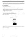
CHAPTER 1 OVERVIEW
The MINICUBE is an emulator to be connected to a target device with an on-chip debug unit to efficiently debug
hardware and software.
1.1 Features
{ USB connection
The MINICUBE can be connected to the host machine via the USB interface (1.1/2.0).
Since it operates on power supplied via USB, an external power supply is unnecessary.
{ On-chip debugging
Debugging is possible with the target microcontroller mounted on the target system.
Programs can be downloaded (programming) to the flash memory by using the flash self programming function
of the microcontroller.
{ N-Wire interface, Nexus interface
<R>
Using a JTAG- and Nexus-compliant and Nexus interface, the QB-V850MINI can be used generally for
V850E2M, V850E2, V850E1 and V850ES microcontrollers with the on-chip debug unit.
The MINICUBE is a successor of the IE-V850E1-CD-NW (PCMCIA type), so that the debugging environment for
the IE-V850E1-CD-NW can be ported as is to the QB-V850MINI.
Note that the IE-V850E1-CD-NW cannot be used with V850E2M microcontrollers.
{ Inclusion of self-check board
Using the self-check board that is supplied with the MINICUBE can perform self-testing for faults.
The self-check board can also be used as the debug adapter for the V850ES/KJ1(+), V850ES/KG1(+),
V850ES/KF1(+), and V850ES/KE1(+).
10
User’s Manual R20UT0221EJ0301
CHAPTER 1 OVERVIEW
1.2 Before Using QB-V850MINI
Be sure to confirm the package contents listed in this chapter before using the MINICUBE.
To utilize this document effectively, familiarize yourself with the usage purposes of the MINICUBE described in this
chapter.
1.2.1 Package contents
When purchasing MINICUBE, be sure to check that all the items listed in the packing specifications are included.
These items may differ depending on the region, but the MINICUBE package usually contains the items shown below.
If there are missing or damaged items, please contact a Renesas Electronics sales representative or a Renesas
Electronics distributor. Note that the items in the QB-V850MINI package differ from those in the QB-V850MINIL
package.
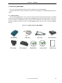
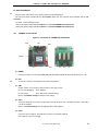
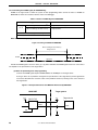
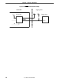
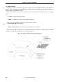
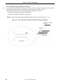
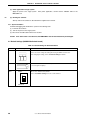
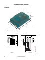
Figure 1-1. Package Contents of QB-V850MINI
QB-V850MINI
KEL adapter
USB cable
KEL connector
OCD cable
ID850QB Disk
User’s Manual R20UT0221EJ0301
Accessory Disk
Self check board
Setup manual
11
CHAPTER 1 OVERVIEW
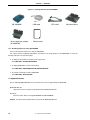
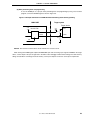
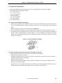
Figure 1-2. Package Contents of QB-V850MINIL
QB-V850MINI
USB cable
16-pin conversion adaptor
(for V850E2M)
OCD cable
Self check board
Setup manual
1.2.2 Checking purpose for using QB-V850MINI
There are mainly three purposes for using the MINICUBE.
The system must be configured appropriately according to each usage purpose of the MINICUBE, so check the
following and refer to the relevant chapter.
{ To debug the target device mounted on the target system
See CHAPTER 3 ON-CHIP DEBUGGING.
{ To debug V850ES/Kx1+ with in-circuit method
See CHAPTER 4 DEBUGGING WITH IN-CIRCUIT METHOD.
{ To perform self-testing for faults in MINICUBE
See CHAPTER 5 SELF-TESTING.
1.3 Supported Devices
See the following MINICUBE Web site or document for the devices supported by the MINICUBE.
MINICUBE Web site:
http://www2.renesas.com/micro/en/development/asia/v850/minicube.html
Document:
Document name: Notes on Using QB-V850MINI and QB-V850MINIL.
Remark The above-mentioned document is posted on the MINICUBE Web site.
12
User’s Manual R20UT0221EJ0301
CHAPTER 1 OVERVIEW
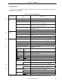
1.4 Specifications
This section describes MINICUBE hardware specifications and specifications for the debug function when using
the ID850QB integrated debugger.
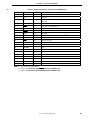
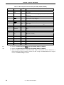
Table 1-1. Hardware Specifications
Classification
<R>
<R>
<R>
<R>
MINICUBE main
unit
Host machine
interface
Target interface
Item
5 V (USB-bus powered type) 500 mA (Max.)
Operating clock
Clock mounted in MINICUBE
Operating environment
Temperature: 0 to +40°C
Humidity: 10 to 80% RH (no condensation)
Storage environment
Temperature: −15 to +40°C
Humidity: 10 to 80% RH (no condensation)
External dimensions
88.5 × 56.5 × 26.1 mm (see APPENDIX B EXTERNAL
DIMENSIONS for details)
Weight
Approximately 90 g
Target host machine
PC98-NX Series, IBM PC/AT
Target OS
Windows 2000, Windows XP, Windows Vista
TM
compatibles
USB
1.1, 2.0
USB cable length
2,000 mm max.
Current consumption
Approximately 350 mm
Target device
Microcontroller with V850E2M, V850E2, V850E1, V850ES Series
on-chip debug unit and microcontroller with Nx85ET core
OCD cable length
200 mm
Clock frequency
Equivalent to specifications supported by the target device
Voltage range
2.0 to 5.5 V
Number of signals occupied for
debugging
V850E2, V850E1, V850ES: 5
V850E2M: 6
V850E2M
signals
DCK
TCK
Clock input
DMS
TMS
Mode select input signal
DDI
TDI
Data input signal
DDO
TDO
Data output signal
DRST
DRST
On-chip debug mode setting signal
-
<R>
Note
Operating power supply
V850E2/V850E1/
V850ES signals
<R>
Specifications
RDY
Synchronous signals
Number of signals used for flash
1
memory writing
Signal for writing to the flash memory
Used when writing to the flash memory from the ID850QB
FLMD0
Number of signals for target power
1
supply detection
Power supply to the target system
Used for monitoring power supplied to the target system
VDD
− (depends on the target connector for OCD)
Number of GND signal lines
GND
GND signal
Number of signals for reset interface
RESET
1
Used for system reset
Note Not all hardware combinations of host machine, USB device, and USB hub are guaranteed to work.
User’s Manual R20UT0221EJ0301
13
CHAPTER 2 NAMES AND FUNCTIONS OF HARDWARE
This chapter describes the part names and functions of the MINICUBE and the self-check board.
The part names described in this chapter are used throughout this document. This chapter provides an overview
of the various functions. Reading it through, the reader will gain a basic grasp of the MINICUBE and the self-check
board that will facilitate reading of subsequent chapters. Also check the hardware while reading this chapter: This
way you may detect damage, if any, and this prevents adverse effects on the system.
14
User’s Manual R20UT0221EJ0301
CHAPTER 2 NAMES AND FUNCTIONS OF HARDWARE
2.1 Names of Parts in Main Unit
The part names and functions of the MINICUBE are described below.
Figure 2-1. Names of Parts in MINICUBE
(a) Main unit (top view)
ON
12345678
SW1
(inside the unit)
OCD connector
USB connector
S
ET
U
AT
ST
G
R
TA
ER
W
PO
Screw
LED
(b) Left side
USB connector
(c) Right side
Screw
User’s Manual R20UT0221EJ0301
OCD connector for MINICUBE
15
CHAPTER 2 NAMES AND FUNCTIONS OF HARDWARE
(1) SW1
Switches used for performing the initial settings for the MINICUBE. They are set to OFF by default.
Refer to 3.2.2 Switch settings for details on the settings.
(2) USB connector
A connector used for connecting the USB interface cable.
(3) OCD connector
A connector used for connecting the OCD cable.
(4) Screw
A screw used for fixing the MINICUBE main unit.
(5) LED
The meanings of each LED are listed below.
Display Name
Lit/Extinguished
Meaning
POWER
Lit
The power supply to the MINICUBE is on.
Extinguished
The power supply to the MINICUBE is off.
TARGET
Lit
The power supply to the target system is on.
Extinguished
The power supply to the target system is off, or the target system is not
connected to QB-V850MINI.
STATUS
<R>
16
Lit
The QB-V850MINI is running.
Extinguished
The QB-V850MINI is in the break state, or the debugger is not active.
OVER VOLTAGE
Lit
Overvoltage of 6.5 V or higher is being applied from the target system.
(QB-V850MINIL only)
Extinguished
Voltage is being applied normally from the target system.
User’s Manual R20UT0221EJ0301
CHAPTER 2 NAMES AND FUNCTIONS OF HARDWARE
2.2 Self-Check Board
<R>
The part names and functions of the self-check board are described below.
The self-check board included with the QB-V850MINI differs from the self-check board included with the QBV850MINIL.
For details, see the following sections.
• Self-check board included with QB-V850MINI: See 2.2.1 QB-V850MINI self-check board.
• Self-check board included with QB-V850MINI: See 2.2.2 QB-V850MINI self-check board.
2.2.1
V850MINI self-check board
Figure 2-2. Part Names of V850MINI Self-Check Board
FW1
OSC2
OSC1
NWIRE1
SW1
U1
CN3
CN2
CN1
(1) NWIRE1
A connector used for connecting the MINICUBE (HIF3FC-20PA-2.54DSA: made by Hirose Electric Co., Ltd).
(2) FW1
<R>
A connector used for connecting the flash memory programmer.
(3) SW1
A switch used to set connection or disconnection of the target system.
For in-circuit debugging:
Set to “Adapter”.
For self-testing:
Set to “Self Check”. (Default setting)
Refer to 4.3.4 Switch settings for details on the settings.
(4) OSC1
A resonator board for the ceramic resonator that is used for the main clock. An 8 MHz resonator is mounted in
a socket at shipment.
Refer to 4.3.3 Clock settings when changing the main clock frequency.
(5) OSC2
A resonator for the subclock. A 32.768 kHz resonator is mounted at shipment.
The frequency cannot be changed.
User’s Manual R20UT0221EJ0301
17
CHAPTER 2 NAMES AND FUNCTIONS OF HARDWARE
(6) U1
V850ES/KJ1+ (The μPD70F3318YGJ) is mounted.
(7) CN1, CN2, CN3
Connectors used for connecting the MINICUBE to the target system.
An exchange adapter and a target connector are required separately.
<R>
2.2.2
V850MINIL self-check board
Figure 2-2. Part Names of V850MINIL Self-Check Board
FW1
X1
U1
NWIRE1
(1) NWIRE1
A connector used for connecting the MINICUBE.
(2) FW1
A connector used for connecting the flash memory programmer.
(3) X1
The main clock. A 5 kHz resonator is mounted at shipment.
(6) U1
V850ES/JF3-L (The μPD70F3736GK) is mounted.
18
User’s Manual R20UT0221EJ0301
CHAPTER 3 ON-CHIP DEBUGGING
This chapter describes how to use the QB-V850MINI when performing on-chip debugging (OCD).
On-chip debugging is a method to debug a microcontroller mounted on the target system. Since debugging is
performed with the real device operating on the board, this method is suitable for field debugging.
<R>
On the other hand, on-chip debugging takes up five or six function pins for communication with the host machine.
Moreover, communication circuits must be mounted on the target system.
Refer to 3.4 Designing Target System Circuits for information on designing target system circuits. Also refer to
the user’s manual for the target device.
Refer to 3.5 Target Connectors for OCD for the target connectors for OCD that can be mounted on the target
board.
User’s Manual R20UT0221EJ0301
19
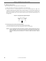
CHAPTER 3 ON-CHIP DEBUGGING
3.1 System Configuration
This section describes the system configuration for performing on-chip debugging.
The system configuration differs depending on whether debugging is being performed in a V850E2M environment
<R>
or in a V850E2, V850E1, or V850ES environment. For the former, see 3.1.1 System configuration in V850EM
environment, and for the latter, see 3.1.2 System configuration in V850E2, V850E1, or V850ES environment.
<R>
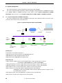
3.1.1 System configuration in V850EM environment
The system configuration when using the V850E2M is shown below. The components used for connection can be
selected to suit the features of the system being used.
Figure 3-1. System Configuration When Using V850E2M
OCD cable
MINICUBE
USB cable
Host macnine
16-pin
Mictor
adapter
conversion
adapter
16-pin
20-pin
general-purpose
connector
general-purpose
connector
Mictor connector
SICA
adapter
SICA connector
Common parts
• Host machine: For software tool operation
• USB cable: Connects the host machine to the MINICUBE main unit.
• MINICUBE main unit: On-chip debug emulator main unit.
• OCD cable: Connects MINICUBE to the target system.
Connection parts
• 16-pin conversion adapter: Used to connect the OCD cable to a 16-pin general-purpose connector.
Included with the QB-V850MINIL but not with the QB-V850MINI.
• 16-pin general-purpose connector: A 16-pin male connector with a pitch of 2.54 mm. Sold separately.
• 20-pin general-purpose connector: A 20-pin male connector with a pitch of 2.54 mm. Sold separately.
• Mictor adapter: Used to connect the OCD cable to a Mictor connector. Sold separately.
• Mictor connector: A connector that supports a high-speed interface. Sold separately.
A debugging tool with tracing capability sold by a Renesas Electronics partner company can also
be connected to this connector.
• SICA adapter: Used to connect the OCD cable to an SICA connector. Sold separately.
• SICA connector: A small, space-saving connector. Sold separately.
20
User’s Manual R20UT0221EJ0301
CHAPTER 3 ON-CHIP DEBUGGING
<R>
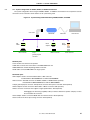
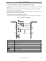
3.1.2 System configuration in V850E2, V850E1, or V850ES environment
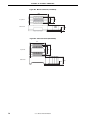
The system configuration when using the V850E2, V850E1, or V850ES is shown below. The components used for
connection can be selected to suit the features of the system being used.
Figure 3-2. System Configuration When Using V850E2, V850E1, or V850ES
OCD cable
MINICUBE
KEL
adater
USB cable
SICA
adapter
Mictor
adapter
KEL connector
20-pin
Host machine
Mictor connector
SICA connector
general-purpose
connector
Common parts
• Host machine: For software tool operation
• USB cable: Connects the host machine to the MINICUBE main unit.
• MINICUBE main unit: On-chip debug emulator main unit.
• OCD cable: Connects MINICUBE to the target system.
Connection parts
• KEL adapter: Used to connect the OCD cable to a KEL connector.
Included with the QB-V850MINI but not with the QB-V850MINIL.
• KEL connector: Standard connector for V850E2, V850E1, or V850ES. Sold separately.
Included with the QB-V850MINI but not with the QB-V850MINIL.
• 20-pin general-purpose connector: A 20-pin male connector with a pitch of 2.54 mm. Sold separately.
• Mictor adapter: Used to connect the OCD cable to a Mictor connector. Sold separately.
• Mictor connector: A connector that supports a high-speed interface. Sold separately.
A debugging tool with tracing capability sold by a Renesas Electronics partner company can also
be connected to this connector.
• SICA adapter: Used to connect the OCD cable to an SICA connector. Sold separately.
• SICA connector: A small, space-saving connector. Sold separately.
User’s Manual R20UT0221EJ0301
21
CHAPTER 3 ON-CHIP DEBUGGING
3.2 Setup Procedure
This section describes the MINICUBE setup procedure to operate the MINICUBE normally. Perform setup using
the following procedure.
Installation of software
<R>
Install the USB driver, software tool, etc., in the host machine.
See 3.2.1 Installation of software.
Proceed to the next step if installation of software has already been completed.
Setting of switch
Set SW1.
This step is not necessary when using a connector other than the MIictor connector as the target connector.
See 3.2.2 Switch settings to perform setting in the correct order.
Connection and startup of system
Connect the host machine, MINICUBE, and target system and start the entire system.
See 3.2.3 Connection and startup of system to perform setting in the correct order.
System shutdown
Shut down the system to terminate debugging.
See 3.2.4 System shutdown.
22
User’s Manual R20UT0221EJ0301
CHAPTER 3 ON-CHIP DEBUGGING
3.2.1 Installation of software
<R>
Install the following software tool in the host machine before setting up the hardware. Refer to the “Setup manual”
supplied with the MINICUBE for the procedures.
• USB driver
• Debugger
• Device file
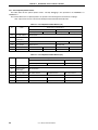
3.2.2 Switch settings
Set SW1. SW1 is mounted inside the MINICUBE main unit. Loosen the screw, open the cover, and then set SW1.
Change the SW1 setting only when all the following conditions are satisfied; otherwise, use the MINICUBE with the
default setting (all “OFF”).
• A Mictor connector is used as the target connector.
• A Renesas Electronics partner company’s emulator that supports the trace interface is used together with the
MINICUBE.
• Pin 20 of the Mictor connector is used as TRCCE (trace compression enable input).
When all the above conditions are satisfied, set SW1 as follows.
Table 3-1. SW1 Setting (When Conditions Are Satisfied)
SW1 Number
Setting
Remark
1 to 7
OFF
Default setting. Any other settings are prohibited.
8
ON
Setting to turn off the power supply to the self-check board
User’s Manual R20UT0221EJ0301
23
CHAPTER 3 ON-CHIP DEBUGGING
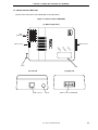
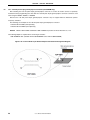
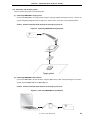
3.2.3 Connection and startup of system
Connect and start the system in the following order.
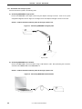
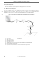
(1) Connecting MINICUBE to target system
Connect the MINICUBE to the target system using the adapter and target connector. Refer to the system
configuration diagrams shown in Figure 3-1 and Figure 3-2 for the adapter and target connector to be used.
Caution Perform connection while the power to the target system is off.
Figure 3-3. Connecting MINICUBE to Target System
Target system
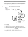
(2) Connecting MINICUBE to host machine
Connect the MINICUBE to the host machine using a USB interface cable. After performing this connection,
confirm that the POWER LED on the MINICUBE is lit.
Caution Perform connection while the power to the target system is off.
Figure 3-4. Connecting MINICUBE to Host Machine
24
User’s Manual R20UT0221EJ0301
CHAPTER 3 ON-CHIP DEBUGGING
(3) Power application to target system
Apply the power to the target system.
After power application, confirm that the TARGET LED on the
MINICUBE is lit.
When using the QB-V850MINIL, if the yellow LED is on, it means that an overvoltage may be being applied.
<R>
Check the target system's power supply and make sure that an appropriate voltage is being applied.
<R>
(4) Running the software
Start up and run the software as described in the supplied user's manual.
3.2.4 System shutdown
Terminate debugging and shutdown the system in the following order.
<R>
(1) Terminate the the software tool.
(2) Turn off the power to the target system.
(3) Disconnect the USB cable from the host machine.
3.3 Default Setting
Item
SW1
Setting
Description
All of switches 1 to 8 are set to OFF by default.
Refer to 3.2.2 Switch settings for how to set the switches.
User’s Manual R20UT0221EJ0301
25
CHAPTER 3 ON-CHIP DEBUGGING
<R>
3.4 Designing Target System Circuits when Using V850E2M
To debug the target system with the MINICUBE connected, a circuit to connect the MINICUBE is required on the
target system.
This section presents information required for circuit design. Read this information together with the information
described in the user’s manual of the target device.
Note that circuit design information when the target device is the V850E2, V850E1, or V850ES is described in 3.5
Designing Target System Circuits When Using V850E2, V850E1, or V850ES.
3.4.1 Example of circuit design (for V850E2M only)
Figure 3-5 illustrates an example of the design of a target system circuit that is used to connect the MINICUBE.
To determine the resistance of the resistors in the circuit, see the user’s manual of the target device.
Figure 3-5. Circuit Connection Example
On-chip debug
emulator
Microcontoroler
EVDD
VDD
TRST
TRST
<R>
TCK
TCK
TMS
TMS
TDI
TDI
TDO
TDO
RDY
RDY
RESET
FLMD0
FLMD0
GND
VSS
Signal Name
26
Outline of Signal
TCK
Clock for the debug control unit (DCU) in the target device
TMS
DCU mode selection signal
TDI
Data signal transmitted to DCU
TDO
Data signal transmitted from DCU
TRST
DCU reset signal
RDY
Synchronous signals
FLMD0
Flash programming mode setting signal
RESET
System reset input signal
VDD
Power supply (The QB-V850MINI uses this signal for detection of target system power supply)
GND
GND
User’s Manual R20UT0221EJ0301
CHAPTER 3 ON-CHIP DEBUGGING
<R>
3.4.2 Cautions on target system design (for V850E2M only)
Note the following points when designing the target system circuits and the board.
(1) Keep the pattern length as short as possible.
(2) If VDD is between 2.0 and 5.5 V, it is judged that target system power is being supplied, and the signals switch
to being used as debug signals. If VDD is not between 2.0 and 5.5 V, it is judged that the system has not been
configured correctly, regardless of whether target system power is being supplied or not. In this case, the
DRST, DCK, DMS, DDI, FLMD0, and RESET pins become high impedance, regardless of the operating status
of the debugger. To avoid this, be sure to input the voltage from the power supply pin on the target device
directly to VDD.
(3) The circuit for connecting FLMD0 varies when using flash self programming or using microcontrollers that do
not have an on-chip flash memory. See 3.4.3 Connecting the FLMD0 signal (for V850E2M only) for details.
(4) To reset the target device while the target system power supply is on, connect the RESET signal.
See 3. 4. 4 Connecting RESET (for V850E2M only) for details.
User’s Manual R20UT0221EJ0301
27
CHAPTER 3 ON-CHIP DEBUGGING
3.4.3 Connecting the FLMD0 signal (for V850E2M only)
FLMD0 is the signal used to switch the system to flash programming mode. Control the status of FLMD0 on
MINICUBE as follows in accordance with the status of the debugger.
Table 3-2. Status of FLMD0 Signal on MINICUBE
Status of FLMD0
Debugger Status
During
When writing to the flash memory
a break
Note
When not writing to the flash memory
High-level (CMOS output)
High impedance
While the user-created program is executing
Terminated
Note When downloading a program or when writing in the Assemble or Memory window.
Figure 3-6. Timing of FLMD0 on MINICUBE
When rewriting the flash memory
during a break
FLMD0
Hi-Z
High level
Hi-Z
Handle the FLMD0 signal as shown in either (a) or (b) below. Whether the FLMD0 signal needs to be connected or
not depends on the specifications of the target device.
(a) When not performing flash self programming
Connect the FLMD0 signal output from MINICUBE to the FLMD0 pin on the target device.
As long as there are no problems arising from the specifications of the target device, pull the signal down
to low level. Determine the resistance value of the pull-down resistor by referring to the user's manual of
the target device.
Figure 3-7. Example Connection of FLMD0 Pin When Used by MINICUBE
MINICUBE
3.3 V
Target system
VDD
74LVC1T45
FLMD0
DIR
28
User’s Manual R20UT0221EJ0301
Target device
FLMD0
CHAPTER 3 ON-CHIP DEBUGGING
(b) When performing flash self programming
To use the FLMD0 pin as a port pin when performing flash self programming by using a user-created
program, connect the FLMD0 signal as shown in Figure 3-8.
Figure 3-8. Example Connection of FLMD0 Pin When Performing Flash Self Programming
Target system
MINICUBE
Target device
3.3V
VDD
74LVC1T45
PORT
R1
FLMD0
FLMD0
R2
DIR
Remark The resistance of R2 must be at least 10 times the resistance of R1.
When leaving the FLMD0 signal output from MINICUBE open and connecting a port signal to FLMD0 on the target
device, set the output of the port to high level in the SFR or other debugger window when writing to the flash memory
during a break. When not writing to the flash memory, set the port output to low level or set the port to input mode.
User’s Manual R20UT0221EJ0301
29
CHAPTER 3 ON-CHIP DEBUGGING
3.4.4 Connecting the RESET signal (for V850E2M only)
To reset the target device while the target system power supply is on, connect the reset signal output from
MINICUBE to the RESET pin on the target device. The RESET signal timing and an example connection circuit are
shown below.
Figure 3-9. Timing of RESET on MINICUBE
Target system power turned on
Software starts up (debugger starts running))
Software terminates (debugger stops running)
Target system power turned off
RESET
Low level
Hi-Z
Hi-Z
Low level
Hi-Z
Figure 3-10. RESET Pin Connection Example
MINICUBE
Target system
VDD
3.3 V
Target device
74LVC1T45
RESET
DIR
30
VDD
User’s Manual R20UT0221EJ0301
RESET
CHAPTER 3 ON-CHIP DEBUGGING
3.5 Designing Target System Circuits When Using V850E2, V850E1, or V850ES
To debug the target system with the MINICUBE connected, a circuit to connect the MINICUBE is required on the
target system.
This section presents information required for circuit design. Read this information together with the information
described in the user’s manual of the target device.
Note that circuit design information when the target device is the V850E2, V850E1, or V850ES is described in 3.4
Designing Target System Circuits When Using V850E2M.
3.5.1 Example of circuit design (for V850E2, V850E1, or V850ES)
Figure 3-11 illustrates an example of the design of a target system circuit that is used to connect the MINICUBE.
Figure 3-11. Circuit Connection Example
VDD
Target device
MINICUBE
DCK
DCK
DMS
DMS
DDI
DDI
DDO
DDO
DRST
DRST
FLMD0
FLMD0
VDD
RESET
RESET
VDD
VDD
GND
Signal Name
Outline of Signal
DCK
Clock for the debug control unit (DCU) in the target device
DMS
DCU mode selection signal
DDI
Data signal transmitted to DCU
DDO
Data signal transmitted from DCU
DRST
DCU reset signal
FLMD0
Flash programming mode setting signal
RESET
System reset input signal
VDD
Power supply (The QB-V850MINI uses this signal for detection of target system power supply)
GND
GND
User’s Manual R20UT0221EJ0301
31
CHAPTER 3 ON-CHIP DEBUGGING
3.5.2 Cautions on target system design (for V850E2, V850E1, or V850ES)
Note the following points when designing the target system circuits and the board.
(1) Keep the pattern length as short as possible.
(2) If VDD is between 2.0 and 5.5 V, it is judged that target system power is being supplied, and the signals switch
to being used as debug signals. If VDD is not between 2.0 and 5.5 V, it is judged that the system has not been
configured correctly, regardless of whether target system power is being supplied or not. In this case, the
DRST, DCK, DMS, DDI, FLMD0, and RESET pins become high impedance, regardless of the operating status
of the debugger. To avoid this, be sure to input the voltage from the power supply pin on the target device
directly to VDD.
(3) The circuit for connecting FLMD0 varies when using flash self programming or using microcontrollers that do
not have an on-chip flash memory. See 3.5.3 (7) FLMD0 for details.
(4) To reset the target device while the target system power supply is on, connect the RESET signal. See 3. 5. 4
Connecting RESET for details.
32
User’s Manual R20UT0221EJ0301
CHAPTER 3 ON-CHIP DEBUGGING
3.5.3 Connecting the FLMD0 signal (for V850E2, V850E1, or V850ES)
FLMD0 is the signal used to switch the system to flash programming mode. Control the status of FLMD0 on
MINICUBE as follows in accordance with the status of the debugger.
Table 3-3. Status of FLMD0 Signal on MINICUBE
Status of FLMD0
Debugger Status
During
When writing to the flash memory
a break
Note
When not writing to the flash memory
High-level (CMOS output)
High impedance
While the user-created program is executing
Terminated
Note When downloading a program or when writing in the Assemble or Memory window.
Figure 3-12. Timing of FLMD0 on MINICUBE
When rewriting the flash memory
during a break
FLMD0
Hi-Z
High level
Hi-Z
Handle the FLMD0 signal as shown in either (a) or (b) or (C) below. Whether the FLMD0 signal needs to be
connected or not depends on the specifications of the target device.
(a) When not performing flash self programming
Connect the FLMD0 signal output from MINICUBE to the FLMD0 pin on the target device.
As long as there are no problems arising from the specifications of the target device, pull the signal down
to low level. Determine the resistance value of the pull-down resistor by referring to the user's manual of
the target device.
Figure 3-13. Example Connection of FLMD0 Pin When Used by MINICUBE
MINICUBE
3.3 V
Target system
VDD
74LVC1T45
FLMD0
Target device
FLMD0
DIR
User’s Manual R20UT0221EJ0301
33
CHAPTER 3 ON-CHIP DEBUGGING
(b) When performing flash self programming
To use the FLMD0 pin as a port pin when performing flash self programming by using a user-created
program, connect the FLMD0 signal as shown in Figure 3-8.
Figure 3-14. Example Connection of FLMD0 Pin When Performing Flash Self Programming
Target system
MINICUBE
Target device
3.3V
VDD
74LVC1T45
PORT
R1
FLMD0
FLMD0
R2
DIR
Remark The resistance of R2 must be at least 10 times the resistance of R1.
When leaving the FLMD0 signal output from MINICUBE open and connecting a port signal to FLMD0 on
the target device, set the output of the port to high level in the SFR or other debugger window when
writing to the flash memory during a break. When not writing to the flash memory, set the port output to
low level or set the port to input mode.
(c) When performing flash self programming
The FLMD0 pin is not required to be connected.
34
User’s Manual R20UT0221EJ0301
CHAPTER 3 ON-CHIP DEBUGGING
3.5.4 Connecting the RESET signal (for V850E2, V850E1, or V850ES)
This is the system reset input signal. The MINICUBE controls the RESET signal as follows.
Figure 3-15. Timing of RESET on MINICUBE
Target system power turned on
Software starts up (debugger starts running))
Software terminates (debugger stops running)
Target system power turned off
RESET
Hi-Z
Hi-Z
Low level
Low level
Hi-Z
Connect the RESET signal as shown in Figure 3-13 if any of the conditions listed below is satisfied. At this
time, make sure that the RESET signal does not conflict with the RESET signal generated on the target
system. When none of the following conditions are satisfied, leave open the pin for the RESET signal that is
output from the MINICUBE.
• The target device should be kept in the reset state before debugger startup or after debugger termination.
• The OCD signal pins (DCK, DDI, DDO, DMS, and DRST) are alternate-function pins in the specifications of
the target device, the OCD signal becomes inactive due to a reset by other than the RESET pin, and the
OCD signals are not set to active in the startup routine.
For example, when using a device in which the pins that alternately function as the OCD signal pins are
controlled by the OCDM0 register as shown below, the OCDM0 register is cleared to 0 upon reset by POC,
so the OCD signals are not specified and as a result, on-chip debugging cannot be performed normally.
OCDM
7
6
5
4
3
2
1
0
0
0
0
0
0
0
0
OCDM0
OCDM0
Specification of alternate-function pin for on-chip debug function
0
Use as port/peripheral function pin
1
Use as on-chip debug function pin
Remark
Initial value
At RESET pin input: OCDM0 = 1
After reset by POC: OCDM0 = 0
After internal reset (other than POC): The OCDM register holds the value before reset
User’s Manual R20UT0221EJ0301
35
CHAPTER 3 ON-CHIP DEBUGGING
Figure 3-16. RESET Pin Connection Example
MINICUBE
Target system
VDD
3.3 V
Target device
74LVC1T45
RESET
DIR
36
VDD
User’s Manual R20UT0221EJ0301
RESET
CHAPTER 3 ON-CHIP DEBUGGING
3.6 Target Connectors for OCD
A target connector for OCD must be mounted on the target system in order to connect the MINICUBE to the target
system. The target connector for OCD can be selected from the target connectors listed in the table below. The
features of each target connector are described in the following sections.
<R>
Table 3-4. List of Target Connectors for OCD (Part Number and Manufacturer)
Target Connector Name
Part Number
KEL connector (cannot be used
8830E-026-170S (included with QB-V850MINI)
when using V850E2M)
8830E-026-170L
Adapter
Manufacturer
KEL Corporation
QB-V850MINIL-AK1 (included with QB-V850MINI)
Renesas Electronics Corporation
2-767004-2
Tyco Electronics AMP K.K.
QB-V850MINIL-AM1
Renesas Electronics Corporation
SICA2P20S05 (5 set)
Tokyo Eletech Corporation
SICA2012P (included with SICA2P20S)
Tokyo Eletech Corporation
2.54 mm pitch 16-pin general-
HIF3FC-16PA-2.54DS
Hirose Electronic Co., Ltd.
purpose connector (cannot be used
HIF3FC-16PA-2.54DSA
(for example)
QB-V850MINIL-AG1 (inclued with QB-V850MINIL)
Renesas Electronics Corporation
2.54 mm pitch 20-pin general-
HIF3FC-20PA-2.54DS
Hirose Electronic Co., Ltd.
purpose connector
HIF3FC-20PA-2.54DSA
(for example)
Mictor connector
Adapter
SICA connector
Adapter
when using V850E2, V850E1, or
V850ES)
Adapter
Adapter
Not required
User’s Manual R20UT0221EJ0301
−
37
CHAPTER 3 ON-CHIP DEBUGGING
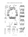
3.6.1 KEL connector (for V850E2, V850E1, or V850ES)
<R>
A KEL connector is a target connector included with the QB-V850MINI but not with the QB-V850MINIL.
Note that the KEL connector cannot be used when using the V850E2M.
When using the KEL connector as the target connector for OCD, mount either of the following connectors on the
target system.
• 8830E-026-170S: 26-pin straight type (included with QB-V850MINI)
<R>
• 8830E-026-170L: 26-pin right-angle type (sold separately)
Remark
8830E-026-170S and 8830E-026-170L are products of KEL Corporation.
A conversion adapter is
included with the QB-V850MINI.
Figure 3-17 and Table 3-5 show the pin assignment and the pin functions of the KEL connector, respectively.
Input/output is indicated as seen from the target device.
Figure 3-17. KEL Connector Pin Assignment Diagram
Target system
38
User’s Manual R20UT0221EJ0301
CHAPTER 3 ON-CHIP DEBUGGING
Table 3-5. KEL Connector Pin Functions (for V850E2, V850E1, or V850ES)
Pin No.
A1 to A6
Note 1
Signal Name
I/O
−
GND
Description
Connect to GND
A7
DDI
IN
Data input
A8
DCK
IN
Clock input
A9
DMS
IN
Transfer mode selection input
A10
DDO
OUT
Data output
A11
DRST
IN
Reset input to on-chip debug unit
A12
RESET
IN
System reset input (leave open when not used)
A13
FLMD0
IN
Flash mode input (leave open when not used)
B1 to B10
GND
−
Connect to GND
B11
PORT0_IN
−
Connect to GND
B12
PORT1_IN
−
Connect to GND
B13
VDD
−
Connect to VDD for on-chip debugging (for target system power ON
Note 2
Note 3
monitoring)
Notes 1. As seen from the target device
<R>
2. Refer to 3.5.4 Connecting the RESET signal (for V850E2, V850E1, or V850ES).
<R>
3. Refer to 3.5.3 Connecting the FLMD0 signal (for V850E2, V850E1, or V850ES).
User’s Manual R20UT0221EJ0301
39
CHAPTER 3 ON-CHIP DEBUGGING
3.6.2 Mictor connector
The Mictor connector is conventionally supported as a target connector for OCD that supports the high-speed trace
<R>
interface. When combining use of MINICUBE and an emulator with tracing capability sold by Renesas Eloctronics
partner company, use the Mictor connector.
When using the Mictor connector as the target connector for OCD, mount the following connector on the target
system.
• 2-767004-2: 38-pin type (sold separately)
Remark
2-767004-2 is a product of Tyco Electronics AMP K.K.
Either of the following adapter is required for connection with the emulator.
• QB-V850MINIL-AM1 (sold separately)
<R>
Remark
QB-V850MINIL-AM1 is products of Renesas Electronics Corporation
Figure 3-18 and Table 3-6 show the pin assignment and the pin functions of a target connector for OCD,
respectively. Input/output is indicated as seen from the target device.
Figure 3-18. Mictor Connector Pin Assignment Diagram
Target system
40
User’s Manual R20UT0221EJ0301
CHAPTER 3 ON-CHIP DEBUGGING
Table 3-6. Mictor Connector Pin Functions (for V850E2M only)
<R>
Pin No.
Note 1
Signal Name
1 and 2
GND
3
TCK
4
VDD
I/O
Description
−
Connect to GND
−
Connect to VDD for on-chip debugging (for target system power ON
IN
Clock input
monitoring)
5
TMS
IN
Transfer mode selection input
6
TRST
IN
Reset input to on-chip debug unit
7
TDI
IN
Data input
8
RESET
IN
System reset input (leave open when not used)
9
TDO
OUT
Data output
10
FLMD0
IN
Flash mode input (leave open when not used)
−
11
RESERVE
12
RDY
13
RESERVE
−
Open
14
RESERVE
−
Open
15
RESERVE
−
Open
16
RESERVE
−
Open
17
RESERVE
−
Open
18
RESERVE
−
Open
19
RESERVE
−
Open
20
RESERVE
−
Open
21 to 36
RESERVE
−
Open
37, 38
GND
−
Connect to GND
Note 2
Note 3
Open
OUT
Synchronous signals
Notes 1. As seen from the target device.
2. Refer to 3.4.4 Connecting the RESET signal (for V850E2M only).
3. Refer to 3.4.3 Connecting the FLMD0 signal (for V850E2M only).
User’s Manual R20UT0221EJ0301
41
CHAPTER 3 ON-CHIP DEBUGGING
Table 3-7. Mictor Connector Pin Functions (for V850E2, V850E1, V850ES)
Pin No.
Note 1
Signal Name
1 and 2
GND
3
DCK
4
VDD
I/O
Description
−
Connect to GND
IN
Clock input
−
Connect to VDD for on-chip debugging (for target system power ON
monitoring)
5
DMS
IN
Transfer mode selection input
6
DRST
IN
Reset input to on-chip debug unit
7
DDI
IN
Data input
8
RESET
IN
System reset input (leave open when not used)
9
DDO
OUT
Data output
10
FLMD0
IN
Flash mode input (leave open when not used)
11
N.C
−
Open (not connected)
12
RESERVE
−
Open
13
N.C
−
Open (not connected)
14
PORT0_IN
−
Connect to GND
15
N.C
−
Open (not connected)
16
PORT1_IN
−
Connect to GND
17
GND
−
Connect to GND
18
PORT2_IN
−
Connect to GND
19
GND
−
Connect to GND
20
POWER
−
Open
21 to 38
GND
−
Connect to GND
Note 2
Note 3
Note 4
Notes 1. As seen from the target device.
<R>
2. Refer to 3.5.4 Connecting the RESET signal (for V850E2, V850E1, or V850ES).
<R>
3. Refer to 3.5.3 Connecting the FLMD0 signal (for V850E2, V850E1, or V850ES).
4. When the TRCCE signal (trace compression enable input) is connected as the trace interface for a
Renesas Electronics partner company’s emulator, the SW1 settings in the MINICUBE must be changed.
Refer to 3.2.2 Switch settings for details.
42
User’s Manual R20UT0221EJ0301
CHAPTER 3 ON-CHIP DEBUGGING
3.6.3 SICA connector
The SICA connector is a compact target connector. Use of this connector is effective in cases such as when a
mounting area cannot be secured on the target system. Note that the SICA connector may not support Renesas
Electronics partner company’s emulators.
When using the SICA connector as the target connector for OCD, mount the following connector on the target
system.
• SICA2P20S: 20-pin type (sold separately)
Remark
SICA2P20S is a product of Tokyo Eletech Corporation. The ordering code is “SICA2P20S05”, which
is for a set of five units. Contact Tokyo Eletech Corporation to purchase this product.
The following adapter is required for connection with the emulator.
• SICA20I2P (sold separately)
Remark
SICA20I2P is a product of Tokyo Eletech Corporation.
Figure 3-19. SICA Connector Pin Assignment Diagram
Pin 19
Pin 1
SICA2P20S
TOP VIEW
Target system
(TOP VIEW)
Pin 20
Pin 2
User’s Manual R20UT0221EJ0301
43
CHAPTER 3 ON-CHIP DEBUGGING
<R>
Table 3-8. SICA Connector Pin Functions (for V850E2M only)
Pin No.
1
Note 1
Signal Name
I/O
GND
Description
−
Connect to GND
−
Connect to GND
2
TCK
3
GND
IN
Clock input
4
TMS
5
GND
6
TDI
7
GND
8
TRST
9
GND
−
Connect to GND
10
POWER
−
Open
11
GND
−
Connect to GND
12
RESET
13
GND
14
FLMD0
15
GND
−
Connect to GND
16
RDY
−
Synchronous signals
17
GND
−
Connect to GND
18
DDO
19
GND
−
Connect to GND
20
VDD
−
IN
Transfer mode selection input
−
GND
IN
Data input
−
Connect to GND
IN
Reset input to on-chip debug unit
IN
System reset input (leave open when not used)
−
Connect to GND
IN
Flash mode input (leave open when not used)
OUT
Note 3
Data output
Connect to VDD for on-chip debugging (for target system power ON
monitoring)
Notes 1. As seen from the target device.
2. Refer to 3.4.4 Connecting the RESET signal (for V850E2M only).
3. Refer to 3.4.3 Connecting the FLMD0 signal (for V850E2M only).
44
Note 2
User’s Manual R20UT0221EJ0301
CHAPTER 3 ON-CHIP DEBUGGING
Table 3-9. SICA Connector Pin Functions (for V850E2, V850E1, V850ES).
Pin No.
1
Note 1
Signal Name
I/O
Description
−
GND
Connect to GND
2
DCK
3
GND
IN
Clock input
4
DMS
5
GND
6
DDI
7
GND
8
DRST
9
GND
−
Connect to GND
10
RESERVE
−
Open
11
GND
−
Connect to GND
12
RESET
13
GND
14
FLMD0
15
GND
−
Connect to GND
16
RESERVE
−
Open
17
GND
−
Connect to GND
18
DDO
19
GND
−
Connect to GND
20
VDD
−
−
Connect to GND
IN
Transfer mode selection input
−
GND
IN
Data input
−
Connect to GND
IN
Reset input to on-chip debug unit
IN
System reset input (leave open when not used)
−
Note 2
Connect to GND
IN
Flash mode input (leave open when not used)
OUT
Note 3
Data output
Connect to VDD for on-chip debugging (for target system power ON
monitoring)
Notes 1. As seen from the target device.
<R>
2. Refer to 3.5.4 Connecting the RESET signal (for V850E2, V850E1, or V850ES).
<R>
3. Refer to 3.5.3 Connecting the FLMD0 signal (for V850E2, V850E1, or V850ES).
User’s Manual R20UT0221EJ0301
45
CHAPTER 3 ON-CHIP DEBUGGING
<R>
3.6.4 2.54 mm pitch 16-pin general-purpose connector (for V850E2M only)
After attaching the 2.54 mm pitch 16-pin general-purpose connector, it can also be used to connect a separately
sold flash memory programming tool. Note that the 2.54 mm pitch 16-pin general-purpose connector cannot be used
when using the V850E2, V850E1, or V850ES.
Note that the 2.54 mm pitch 16-pin general-purpose connector may not support Renesas Electronics partner
company’s emulators.
The followings are examples of the 2.54 mm pitch 16-pin general-purpose connector.
• HIF3FC-16PA-2.54DS (sold separately)
• HIF3FC-16PA-2.54DSA (sold separately)
Remark
HIF3FC-16PA-2.54DS and HIF3FC-16PA-2.54DSA are products of Hirose Electronic Co., Ltd.
The following adapter is required when connecting an emulator:
• QB-V850MINIL-AG1 (included with the QB-V850MINIL but not with the QB-V850MINI)
Figure 3-20. 2.54 mm Pitch 16-pin General-Purpose Connector Pin Assignment Diagram
46
User’s Manual R20UT0221EJ0301
CHAPTER 3 ON-CHIP DEBUGGING
<R>
Table 3-10. 2.54 mm Pitch 16-pin General-Purpose Connector Pin Functions (for V850E2M only)
Pin No.
Note 1
Signal Name
I/O
Description
−
1
GND
Connect to GND
2
RESET
IN
System reset input (leave open when not used)
3
TDO
OUT
Data output
4
VDD
−
Note 2
Connect to VDD for on-chip debugging (for target system power ON
monitoring)
5
TDI
6
RESERVE
7
TCK
8
RDY
9
TRST
IN
Data input
−
Open
IN
Clock input
−
Synchronous signals
IN
Reset input to on-chip debug unit
10
RESERVE
−
Open
11
RESERVE
−
Open
12
TMS
13
RESERVE
14
FLMD0
IN
Flash mode input (leave open when not used)
15
For MINICUBE2
OUT
Signal of a separately sold QB-MINI2 (MINICUBE2)
16
POWER
IN
Transfer mode selection input
−
Open
−
Note 3
Note 4
Open
Notes 1. As seen from the target device.
2. Refer to 3.4.4 Connecting the RESET signal (for V850E2M only).
3. Refer to 3.4.3 Connecting the FLMD0 signal (for V850E2M only).
4. When using a separately sold QB-MINI2 (MINICUBE2) as the debug tool, connect this signal to the
MINICUBE2. Refer to the MINICUBE2 User's Manual for detail on the connection. When using a
MINICUBE2 as the programming tool, this signal is not required to be connected.
User’s Manual R20UT0221EJ0301
47
CHAPTER 3 ON-CHIP DEBUGGING
3.6.5 2.54 mm pitch 20-pin general-purpose connector
<R>
A 2.54 mm pitch general-purpose connector do not need connection of adaptor. Note that 2.54 mm pitch 20-pin
general-purpose connectors may not support Renesas Electronics partner company’s emulators.
The followings are examples of the 2.54 mm pitch 20-pin general-purpose connector.
• HIF3FC-20PA-2.54DS (sold separately, right-angle type)
• HIF3FC-20PA-2.54DSA (sold separately, straight type)
Remark
HIF3FC-20PA-2.54DS and HIF3FC-20PA-2.54DSA are products of Hirose Electronic Co., Ltd.
Figure 3-21. 2.54 mm Pitch General-Purpose Connector Pin Assignment Diagram
20-pin general purpose
20-pin general-purpose
connector
connector
Target system
Target system
48
User’s Manual R20UT0221EJ0301
CHAPTER 3 ON-CHIP DEBUGGING
Table 3-11. 2.54 mm Pitch General-Purpose Connector Pin Functions (for V850E2M only)
<R>
Pin No.
1
Note 1
Signal Name
I/O
GND
Description
−
Connect to GND
−
Connect to GND
2
TCK
3
GND
IN
Clock input
4
TMS
5
GND
6
TDI
7
GND
8
TRST
9
GND
−
Connect to GND
10
POWER
−
Open
11
GND
−
Connect to GND
12
RESET
13
GND
14
FLMD0
15
GND
−
Connect to GND
16
RDY
−
Synchronous signal
17
GND
−
Connect to GND
18
TDO
19
GND
−
Connect to GND
20
VDD
−
Connect to VDD for on-chip debugging (for target system power ON
IN
Transfer mode selection input
−
GND
IN
Data input
−
Connect to GND
IN
Reset input to on-chip debug unit
IN
System reset input (leave open when not used)
−
Note 2
Connect to GND
IN
Flash mode input (leave open when not used)
OUT
Note 3
Data output
monitoring)
Notes 1. As seen from the target device.
2. Refer to 3.4.4 Connecting the RESET signal (for V850E2M only).
3. Refer to 3.4.3 Connecting the FLMD0 signal (for V850E2M only).
User’s Manual R20UT0221EJ0301
49
CHAPTER 3 ON-CHIP DEBUGGING
Table 3-12. 2.54 mm Pitch General-Purpose Connector Pin Functions (for V850E2, V850E1, V850ES)
Pin No.
1
Note 1
Signal Name
I/O
Description
−
GND
Connect to GND
2
DCK
3
GND
IN
Clock input
4
DMS
5
GND
6
DDI
7
GND
8
DRST
9
GND
−
Connect to GND
10
RESERVE
−
Open
11
GND
−
Connect to GND
12
RESET
13
GND
14
FLMD0
15
GND
−
Connect to GND
16
RESERVE
−
Open
17
GND
−
Connect to GND
18
DDO
19
GND
−
Connect to GND
20
VDD
−
Connect to VDD for on-chip debugging (for target system power ON
−
Connect to GND
IN
Transfer mode selection input
−
GND
IN
Data input
−
Connect to GND
IN
Reset input to on-chip debug unit
IN
System reset input (leave open when not used)
−
Note 2
Connect to GND
IN
Flash mode input (leave open when not used)
OUT
Note 3
Data output
monitoring)
Notes 1. As seen from the target device.
<R>
2. Refer to 3.5.4 Connecting the RESET signal (for V850E2, V850E1, or V850ES).
<R>
3. Refer to 3.5.3 Connecting the FLMD0 signal (for V850E2, V850E1, or V850ES).
50
User’s Manual R20UT0221EJ0301
CHAPTER 4 DEBUGGING WITH IN-CIRCUIT METHOD
This chapter describes how to use the QB-V850MINI for debugging with the in-circuit method.
In the in-circuit method, an emulator is connected in the position where the device is to be mounted.
<R>
<R>
By using the V850MINI self-check board included with the QB-V850MINI or the separately sold QB-V850ESKX1HDA, MINICUBE can be used to debug the target devices shown in 4.1 below. Note that the V850MINIL self-check
board included with the QB-V850MINIL cannot be used for in-circuit emulation.
4.1 Target Devices
Debugging with the in-circuit method can be performed using the MINICUBE for the following target devices.
V850ES/KE1+, V850ES/KF1+, V850ES/KG1+, V850ES/KJ1+
V850ES/KE1Note, V850ES/KF1Note, V850ES/KG1Note, V850ES/KJ1Note
Note
One caution applies to debugging using the V850MINI self-check board included with the QB-V850MINI.
See No. 23 in Table 6-1 for details.
This caution item is not applicable when using the QB-V850ESKX1-DA (sold separately).
Refer to the technical document for the QB-V850ESKX1-DA (ZUD-CD-04-0120) for details.
Consult a Renesas Electronics sales representative or distributor for how to obtain this document.
User’s Manual R20UT0221EJ0301
51
CHAPTER 4 DEBUGGING WITH IN-CIRCUIT METHOD
4.2 System Configuration
This section describes the system configuration for debugging with the in-circuit method.
4.2.1 Minimum system configuration
The system configuration shown in the following figure illustrates the minimum system configuration required for
<R>
debugging with the in-circuit method. Note that items <6> and <7> in Figure 4-1 are not included with the QBV850MINI. Note also that item <5> is included with the QB-V850MINI but not with the QB-V850MINIL.
Figure 4-1. Minimum System Configuration for Debugging with In-Circuit Method
<R>
<1>
<2>
<3>
<4>
<5>
<6>
<7>
Target system
<1> Host machine:
With USB ports
<2> USB cable (accessory)
<3> MINICUBE (this product)
<4> OCD cable (accessory)
<5> V850MINI Self-check board (included with the QB-V850MINI) or QB-V850ESKX1H-DA
<6> Exchange adapter (sold separately)
<7> Target connector (sold separately): A connector mounted on the target system.
52
User’s Manual R20UT0221EJ0301
CHAPTER 4 DEBUGGING WITH IN-CIRCUIT METHOD
4.2.2 System configuration when using optional products
The figure shown below illustrates the system configuration when using optional products. The items enclosed by
dotted lines are the optional products. Applications of the optional products are described on this page. Refer to 4.2.3
List of optional product names for the corresponding product names.
Figure 4-2. System Configuration with Optional Products
<R>
<1>
<2>
<3>
<4>
<5>
<6>
<7>
<10>
Device
<8>
<9>
<11>
Target system
<1> Host machine:
With USB ports
<2> USB (accessory)
<3> MINICUBE (this product)
<4> OCD cable (accessory)
<5> V850MINI Self-check board (accessory) (included with the QB-V850MINI) or QB-V850ESKX1H-DA
<6> Check pin adapter (sold separately): An adapter used for monitoring waveforms with an oscilloscope, etc.
<7> Coaxial type extension probe (sold separately):
A cable used to extend the distance between the emulator
and target system.
<8> Exchange adapter (sold separately)
<9> Space adapter (sold separately):
An adapter used to adjust the height.
<10> Mount adapter (sold separately):
An adapter used to mount the device in the socket.
<11> Target connector (sold separately):
A connector mounted on the target system.
User’s Manual R20UT0221EJ0301
53
CHAPTER 4 DEBUGGING WITH IN-CIRCUIT METHOD
4.2.3 List of optional product names
The tables below list the optional product names. On-chip debugging is also possible for the V850ES/KJ1 or
V850ES/KJ1+.
The external dimensions of optional products are posted on the following Renesas Electronics webpage.
URL: http://www2.renesas.com/micro/en/development/asia/Emulator/IE/iecube.html
Table 4-1. List of Optional Product Names (1/2)
No.
Name
Target Device to Be Emulated
V850ES/KE1, V850ES/KE1+
64-pin GB
<6>
Check pin adapter
QB-144-CA-01
<7>
Extension probe
QB-144-EP-01S
V850ES/KF1, V850ES/KF1+
64-pin GK
80-pin GC
80-pin GK
(coaxial type)
<8>
Exchange adapter
QB-64-EA-01S
QB-80GC-EA-02S
QB-80GK-EA-01S
<9>
Space adapter
QB-64-SA-01S
QB-80-SA-01S
<10>
Mount adapter
QB-64GB-MA-01S
QB-64GK-MA-01S
QB-80GC-MA-01S
QB-80GK-MA-01S
<11>
Target connector
QB-64GB-TC-01S
QB-64GK-TC-01S
QB-80GC-TC-01S
QB-80GK-TC-01S
Table 4-1. List of Optional Product Names (2/2)
No.
Name
Target Device to Be Emulated
V850ES/KG1, V850ES/KG1+
100-pin GC
<6>
Check pin adapter
QB-144-CA-01
<7>
Extension probe
QB-144-EP-01S
100-pin GF
V850ES/KJ1, V850ES/KJ1+
144-pin GJ
(coaxial type)
<8>
Exchange adapter
QB-100GC-EA-01S
<9>
Space adapter
QB-100-SA-01S
<10>
Mount adapter
QB-100GC-MA-01S
QB-100GF-MA-01S
QB-144GJ-MA-01S
<11>
Target connector
QB-100GC-TC-01S
QB-100GF-TC-01S
QB-144GJ-TC-01S
54
QB-100GF-EA-01S
QB-144GJ-EA-02S
QB-144-SA-01S
User’s Manual R20UT0221EJ0301
CHAPTER 4 DEBUGGING WITH IN-CIRCUIT METHOD
4.3 Setup Procedure
This section describes the MINICUBE setup procedure to operate the QB-V850MINI normally. Perform setup
using the following procedure.
Installation of software
Install the USB driver, software tool, etc., in the host machine.
See 4.3.1 Installation of software.
Proceed to the next step if installation of software has already been completed.
Setting of MINICUBE
Set the MINICUBE’s SW1 to the default setting.
See 3.3 Default Setting for the default settings of the MINICUBE.
Setting of clock
At shipment, an 8 MHz resonator (ceramic resonator) is mounted as the main clock in OSC1 on the V850MINI selfcheck board.
Setting of switch
The SW1 settings vary depending on the purpose of use of the V850MINI self-check board.
At shipment, SW1 is set to perform self-testing (self-check mode).
See 4.3.4 Switch settings for details.
Mounting of target connector
Mount the target connector on the target system.
See 4.3.5 Mounting of target connector.
Proceed to the next step if the target connector is already mounted.
Connection and startup of system
Connect the host machine, MINICUBE, V850MINI, self-check board, and target system and start the entire system.
See 4.3.6 Connection and startup of system to perform setting in the correct order.
System shutdown
Shut down the system to terminate debugging.
See 4.3.7 System shutdown to shut down the system in the correct order.
User’s Manual R20UT0221EJ0301
55
CHAPTER 4 DEBUGGING WITH IN-CIRCUIT METHOD
4.3.1 Installation of software
Install the software tool in the host machine before setting up the hardware. Refer to the Setup Manual supplied
with this product for the procedures.
4.3.2 Setting of MINICUBE
Set the MINICUBE to the default setting.
See 3.3 Default Setting for the default settings of the MINICUBE.
4.3.3 Clock settings
The oscillation clock of the target device is set by the clock settings for the V850MINI self-check board.
Main clock oscillation frequency: The frequency can be changed by replacing the resonator mounted in OSC1.
Subclock oscillation frequency: The frequency is fixed to 32.768 kHz. Do not change the frequency.
This chapter explains how to set the main clock.
The main clock oscillation frequency is determined by the clock mounted in OSC1.
An 8 MHz ceramic resonator is mounted at shipment.
There is no need to change the setting when using an 8 MHz resonator.
When changing the setting, remove the 8 MHz resonator from the parts board of OSC1, and insert the relevant
resonator, as shown in Figure 4-3.
Figure 4-3. OSC1 Setting
Resonator
OSC1
X2
X1
μPD70F3318YGJ
A 3-pin resonator with the capacitor can be inserted easily.
When using a resonator other than the 3-pin resonator, a resonator without the capacitor, or the oscillator, the
oscillator must be configured in OSC1.
Refer to the user’s manual of the target device for details on the oscillator.
56
User’s Manual R20UT0221EJ0301
CHAPTER 4 DEBUGGING WITH IN-CIRCUIT METHOD
4.3.4 Switch settings
For the V850MINI self-check board, two types of mode can be selected by setting SW1.
Set SW1 to “Adapter” when performing emulation with the in-circuit method to set the adapter mode.
Table 4-2. SW1 Setting (Self-Check Board)
SW1 Setting
Adapter
Mode
Adapter mode
Description
A setting to set the mode for performing debugging with in-circuit method.
This is the default setting of SW1.
Self Check
Self-check mode
A setting to set the mode for performing self-testing.
This setting is also used to set the mode for writing to the μPD70F3318YGJ
on the V850MINI self-check board using a flash memory programmer.
This mode is used to erase the on-chip flash memory when the debugger
cannot be activated because the user has skipped setting of the security ID
code.
User’s Manual R20UT0221EJ0301
57
CHAPTER 4 DEBUGGING WITH IN-CIRCUIT METHOD
4.3.5 Mounting target connector
Mount the target connector on the target system in the following order.
(1) Apply cream solder to the foot pattern for mounting the IC on the target system.
(2) The target connector has a cylindrical projection in the center of the underside (Figure 4-4). Apply a twocomponent hardening type epoxy adhesive agent (a type that hardens in 15 to 30 minutes) sparingly to the
underside of the projection to temporarily secure the connector at the specified location on the target system.
Make sure that the position of pin 1 of the connector (where the corner is cut) matches the position of pin 1 on
the target board.
Figure 4-4. Target Connector Projection Diagram
(3) Mount the target connector under the following conditions.
a. To mount the target connector by reflow: 245°C within 20 seconds (heating)
b. To mount the target connector by manual soldering: 320°C within 5 seconds (per pin)
Caution The flux splashing that takes place while the connector is being mounted often results in
defective conduction. Be sure to cover the upper part of the connector with aluminum foil.
Avoid flux cleaning since the connector has a structure in which flux solvent is likely to
remain.
58
User’s Manual R20UT0221EJ0301
CHAPTER 4 DEBUGGING WITH IN-CIRCUIT METHOD
4.3.6 Connection and startup of system
Connect and start the system in the following order.
(1) Connecting MINICUBE to target system
Connect the MINICUBE to the target system using the exchange adapter and target connector. Refer to the
system configuration diagrams shown in Figures 4-1 and 4-2 for the connection of other optional products.
Caution Perform connection while the power to the target system is off.
Figure 4-5. Connecting MINICUBE to Target System
Target system
(2) Connecting MINICUBE to host machine
Connect the MINICUBE to the host machine using the USB interface cable. After performing this connection,
confirm that the POWER LED on the MINICUBE is lit.
Caution Perform connection while the power to the target system is off.
Figure 4-6. Connecting MINICUBE to Host Machine
User’s Manual R20UT0221EJ0301
59
CHAPTER 4 DEBUGGING WITH IN-CIRCUIT METHOD
(3) Power application to target system
Apply the power to the target system.
After power application, confirm that the TARGET LED on the
MINICUBE is lit.
(4) Running the software
<R>
Start up and run the software as described in the supplied user's manual.
4.3.7 System shutdown
Terminate debugging and shutdown the system in the following order.
(1) Terminate the software.
(2) Turn off the power to the target system.
(3) Disconnect the USB cable from the host machine.
Caution If the above order is not observed, the MINICUBE or the self-check board may be damaged.
4.4 Default Settings (V850MINI Self-check board)
Table 4-3. Default Settings of Self-Check Board
Item
Setting
Description
An 8 MHz resonator is mounted at shipment.
OSC1
There is no need to change the setting when using an 8 MHz resonator as is.
When changing the setting, refer to 4.3.3 Clock settings for details.
A 32.768 kHz resonator is mounted at shipment.
OSC2
Do not change the frequency.
SW1
Adapter
SW1 is set to “Self Check” by default.
Refer to 4.3.4 Switch settings for how to set the switches.
Self Check
60
User’s Manual R20UT0221EJ0301
CHAPTER 4 DEBUGGING WITH IN-CIRCUIT METHOD
4.5 Cautions on Using Sockets
This section describes cautions on using sockets such as the target connector and exchange adapter.
The following symbols are used in this section.
• TC: Target connector
• EA: Exchange adapter
• MA: Mount adapter
• CA: Check pin adapter
• SA: Space adapter
• EP: Extension probe
4.5.1 Cautions on inserting/removing sockets
• When inserting an adapter such as EA, MA, or SA in TC, insert it so that the position of pin 1 (where the corner
is cut) on each adapter matches. Be sure to insert the connectors in the correct direction (so that the positions
match).
• Remove or insert the sockets in the correct direction (see Figure 4-7).
• Be sure to hold the lower (mating) connector or board with your fingers when inserting or removing a socket.
• Use a bamboo spit or similar object as a tool to remove the connector. Insert the tool between TC and EA and
remove TC in the correction direction as shown in Figure 4-7. If force is applied to the connector in the wrong
direction, the connector will be damaged. If only a metallic object such as a screwdriver is available as leverage,
wrap its tip in a soft cloth.
Figure 4-7. How to Insert/Remove a Socket
4.5.2 Causes of faulty contact of connectors and countermeasures for them
Possible causes of faulty connector contact and countermeasures are listed below.
• If flux gets inside TC when it is mounted
Thoroughly clean the flux with a solvent such as alcohol. Cleaning must be performed at least 5 to 6 times. If
conduction is still not stable, repeat cleaning.
• If dirt gets inside the connector
If dirt, such as threads, gets inside the connector, defective conduction occurs. Remove any dirt with a brush.
• Cautions on using CA, SA, and EP
When CA, SA, or EP is inserted, a very small amount of delay in the signal propagation and capacitance occur.
Thoroughly evaluate these points after CA, SA, or EP is connected to the target system.
User’s Manual R20UT0221EJ0301
61
CHAPTER 4 DEBUGGING WITH IN-CIRCUIT METHOD
4.6 Recovery of Security ID
This section describes how to recover from the case where the software tool cannot be activated because the user
forgot the ID code or has skipped setting of the ID code, when using the V850MINI self-check board.
Perform the following steps to recover from the above cases.
(1) Remove the V850MINI self-check board from the target system.
(2) Set SW1 on the V850MINI self-check board to “Self Check”.
(3) Connect the flash memory programmer to the FW1 connector on the self-check board.
Caution To avoid signal conflicts, do not connect the MINICUBE to the self-check board when the
flash memory programmer is connected.
Do not supply the clock from the flash memory programmer during writing/erasure.
(Use OSC1 on the self-check board as a clock for writing.)
(4) Enter the settings for the flash memory programmer.
Figure 4-8 shows setting examples when using the PG-FPL as the flash memory programmer.
(5) Perform a chip erase operation.
After the chip erasure, the security ID is set to “0xFFFFFFFFFFFFFFFFFFFF”.
Figure 4-8. Example of Settings for PG-FPL (1/2)
62
User’s Manual R20UT0221EJ0301
CHAPTER 4 DEBUGGING WITH IN-CIRCUIT METHOD
Figure 4-8. Example of Settings for PG-FPL (2/2)
User’s Manual R20UT0221EJ0301
63
CHAPTER 5 SELF-TESTING
This chapter describes how to perform self-testing of the MINICUBE.
When the debugger does not operate normally, this function can be used to determine whether the cause lies in
the MINICUBE, or in other hardware.
<R>
5.1 System Configuration
Figure 5-1 illustrates the system configuration for performing self-testing.
Figure 5-1. System Configuration for Self-Testing
<1>
<2>
<3>
<4>
<5>
<1> Host machine:
With USB ports
<2> USB interface cable (accessory)
<3> MINICUBE (this product)
<4> OCD cable (accessory)
<5> Self-check board (accessory)
64
User’s Manual R20UT0221EJ0301
CHAPTER 5 SELF-TESTING
5.2 Setup Procedure
This section describes the MINICUBE setup procedure to operate the MINICUBE normally. Perform setup using
the following procedure.
Installation of software
<R>
Install the USB driver, software tool, etc., in the host machine.
See 5.2.1 Installation of software.
Proceed to the next step if installation of software has already been completed.
Setting of MINICUBE
Set the MINICUBE’s SW1 to the default setting.
See 3.3 Default Setting for the default settings of the MINICUBE.
Setting of self-check board
Set the self-check board to the default setting.
See 4.4 Default Settings for the default settings of the V850MINI self-check board.
Connection and startup of system
Connect the host machine, MINICUBE, and target system and start the entire system.
See 5.2.4 Connection and startup of system to perform setting in the correct order.
System shutdown
Terminate self-testing and shut down the system.
See 5.2.5 System shutdown.
User’s Manual R20UT0221EJ0301
65
CHAPTER 5 SELF-TESTING
5.2.1 Installation of software
Install the following software in the host machine before setting up the hardware. Refer to the “Setup manual”
supplied with the QB-V850MINI for the procedures.
<R>
When using the ID850QB,MULTI(made by Green hills software Co., Ltd).,
The required device file is shown below. This file differs depending on which self-check board is being used. A device
file does not have to be installed when using CubeSuite.
• V850MINIL self-check board: DF703736
• V850MINI self-check board: DF703318
The device file can be downloaded from the following website:
http://www2.renesas.com/micro/en/ods/
5.2.2 Setting of MINICUBE
Set the MINICUBE to the default setting when performing self-testing.
See 3.3 Default Setting for the default settings of the MINICUBE.
5.2.3 Setting of self-check board
Set the self-check board to the default setting when performing self-testing.
See 4.4 Default Settings (V850MINI Self-check board) for the default settings.
5.2.4 Connection and startup of system
Connect and start the system in the following order.
(1) Connecting MINICUBE to self-check board
Connect the MINICUBE to the V850MINI self-check board using the OCD cable.
Caution Do not connect the MINICUBE to the host machine at this time.
Figure 5-2. Connecting MINICUBE to Self-Check Board
66
User’s Manual R20UT0221EJ0301
CHAPTER 5 SELF-TESTING
(2) Connecting MINICUBE to host machine
Connect the MINICUBE to the host machine using the USB interface cable. After performing this connection,
confirm that LEDs (POWER and TARGET) on the MINICUBE are lit.
Figure 5-3. Connecting MINICUBE to Host Machine
(3) Startup of N-Wire Checker
<R>
If CubeSuite has been installed, N-Wire Checker can be started up by clicking Start Æ NEC Electronics
CubeSuite Æ Emulator Utilities Æ V850 Æ N-Wire Checker.
Refer to the following table for the settings to be specified in the main dialog box.
After specifying these settings, proceed according to the instructions in the N-Wire Checker user's manual.
When using
Specify DF3736.800
V850MINIL
Select 5.000 for Main OSC.
self-check
board
Select the ID code check box and input the security code specified at addresses 0x70 to 0x79.
Select IE-V850E1-CD-NW/QB-V850MINI (DCK=20 MHz).
When using
Specify DF3318Y.800
V850MINI
Select 8.000 for Main OSC.
self-check
board
Select the ID code check box and input the security code specified at addresses 0x70 to 0x79.
At shipment, the debugger can be activated by inputting “FFFFFFFFFFFFFFFFFFFF”.Select IEV850E1-CD-NW/QB-V850MINI (DCK=10 MHz).
5.2.5 System shutdown
Terminate self-testing and shutdown the system in the following order.
(1) Terminate the N-Wire Checker.
(2) Disconnect the USB cable from the host machine.
Caution If the above order is not observed, the MINICUBE or the self-check board may be damaged.
User’s Manual R20UT0221EJ0301
67
CHAPTER 6 CAUTIONS
This chapter lists cautions on using the MINICUBE.
Caution items are classified in the following three categories, so refer to the relevant items.
[OCD]
Cautions for performing on-chip debugging
[IE]
Cautions for performing debugging with in-circuit method
[SC]
Cautions for performing self-testing
Table 6-1. List of Cautions (1/2)
No.
1
Classification
[OCD]
Caution
Use of target devices used for on-chip debugging as mass production products is not guaranteed.
Guarantee for the case where only downloading of a program is performed but debugging is not
performed is planned.
2
[OCD]
In a target device that incorporates an OCD unit, some of the target interface signal pins for OCD
may have alternate functions. The alternate functions of these pins cannot be used during on-chip
debugging.
3
[OCD], [IE]
When erasure and write are prohibited by setting the security flag for the flash memory, programs
cannot be downloaded via the debugger.
4
[OCD], [IE]
If DMA transfer to the internal RAM is performed while a program is being downloaded to the flash
memory, downloading of the program may not be performed normally because the integrated
debugger uses the internal RAM during program downloading.
5
[OCD], [IE]
Do not use the ROM correction function or else unexpected breaks will occur.
6
[OCD]
Since the initial value of the ASID register in the V850E1 Series is undefined, set the ASID register
to 00H via the reset routine. Initialization of the V850ES Series is not required.
7
[OCD]
The current consumption in the target device increases during debugging compared with that in
normal operation mode, because the OCD unit of the target device operates during debugging.
8
[OCD]
The break function may malfunctions when a reset occurs during RUN (program execution),
depending on the target device. See the documents of the target device (user’s manual, restriction
notification, etc.).
9
[OCD]
The I/O buffer (port pin) may enter the reset status depending on the target device when a reset is
input from the pin, even if reset is masked by the mask function. See the documents of the target
device (user’s manual, restriction notification, etc.).
10
[OCD]
No break occurs in an interrupt service routine for an interrupt acknowledged during self
programming, even if an event breakpoint has been set.
11
[OCD], [IE]
When using the self programming function, set the debugger so that the clock for the peripheral
macros does not stop during breaks; otherwise, the flash memory may be damaged.
12
[OCD], [IE]
When using the self programming function, do not set software breaks to the ROM area; otherwise,
an unexpected break may occur.
13
[OCD]
With the V850E1 Series, a forced break may be executed via the debugger operation during flash
self writing. After a forced break, reexecute the program via the debugger or reset the CPU.
68
User’s Manual R20UT0221EJ0301
CHAPTER 6 CAUTIONS
Table 6-1. List of Cautions (2/2)
No.
Classification
Caution
14
[IE]
VDD and EVDD are shorted on the self-check board.
Therefore, be sure to input the same voltage level to VDD and EVDD.
15
[IE]
The P05, P52, P53, P54, and P55 pins are used for connecting the on-chip debug emulator, so
these ports cannot be used.
16
[IE]
The X1, X2, XT1, and XT2 pins are not connected to the target system.
Consequently, the oscillation circuit in the target system cannot be used.
17
[IE]
Do not apply a high voltage (5.5 V or higher) to the VPP pin; otherwise, the MINICUBE may be
damaged.
18
[IE]
The REGC pin is not connected to the target system.
The REGC pin is connected to VDD inside the emulator.
19
[IE]
The MINICUBE and the flash memory programmer cannot be connected at the same time.
20
[IE]
The MINICUBE outputs a high-level signal to the FLMD0 pin while a program is being downloaded.
(The MINICUBE output becomes the high-impedance state when no program is being
downloaded.)
Note the FLMD0 pin connection on the target system side.
21
[IE]
When the flash memory programmer is connected, no clock can be supplied from the programmer.
Use a clock on the self-check board (8 MHz at shipment) for writing or erasing data from the flash
memory programmer.
22
[IE]
Note the following points concerning the settings in the Configuration screen when the debugger is
activated.
• “Chip” area
Select the device to be used.
• “Clock” area
Set as follows.
- Main OSC:
Input a frequency of the resonator mounted in OSC1 with the socket
(Input “8” when using OSC1 with the default setting).
- Multiply rate: Input the maximum multiplication rate of the frequency used for the
resonator mounted in OSC1 with the socket.
- Sub OSC:
Input “32.768”.
• “ID Code” area
Input the security code that has been set at addresses 0x70 to 0x79.
At shipment, the debugger can be activated by inputting “FFFFFFFFFFFFFFFFFFFF”.
• “N-Wire I/F” area
Be sure to select “DCK=10MHz”.
The debugger may not operate if “DCK=20MHz” is selected.
Figure 6-1 shows the screen image for the above settings.
23
[IE]
The P00 pin outputs a low-level signal during a reset.
Exercise care when performing emulation of the V850ES/KE1, V850ES/KF1, V850ES/KG1, or
V850ES/KJ1.
24
[SC]
Do not connect the target system when performing self-testing.
User’s Manual R20UT0221EJ0301
69
CHAPTER 6 CAUTIONS
Figure 6-1. Image of Configuration Screen for Caution No. 22
70
User’s Manual R20UT0221EJ0301
APPENDIX A V850MINI SELF-CHECK BOARD CIRCUIT DIAGRAMS
User’s Manual R20UT0221EJ0301
71
APPENDIX B EXTERNAL DIMENSIONS
B.1 MINICUBE
Figure B-1. MINICUBE
26.1 mm
84.5 mm (88.5 mm including screw)
56.5 mm
B.2 V850MINI Self-Check Board
Figure B-2. V850MINI Self-Check Board
FW1
OSC1
48
CN3
16.15
Self
Check
31.85
SW1
U1
Adapter
NWIRE1
NWIRE1
OSC2
FW1
CN2
CN1
10.65
14.85
21.2
25.8
31.95
36.55
47
Top View
Bottom View
(Unit: mm)
72
User’s Manual R20UT0221EJ0301
APPENDIX B EXTERNAL DIMENSIONS
B.3 Target Connectors (for OCD)
The external dimensions described in this section are the dimensions required for the target connector (for OCD)
(unit: mm). Refer to the dimension diagrams supplied by each connector manufacturer when designing boards.
The external dimension diagrams of optional products to be used for emulation with the in-circuit method are
posted on the following Renesas Electronics webpage.
URL: http://www2.renesas.com/micro/en/development/asia/Emulator/IE/iecube.html
Figure B-3. KEL Connector (8830E-026-170S)
31.64
Top View
7
13.7
Side View
3
Figure B-4. KEL Connector (8830E-026-170L)
31.64
17.4
Top View
Side View
10
3
User’s Manual R20UT0221EJ0301
73
APPENDIX B EXTERNAL DIMENSIONS
Figure B-5. Mictor Connector (2-767004-2)
25.4
Top View
6.91
8.72
Side View
1.35 7.34
Figure B-6. SICA Connector (SICA2P20S)
8.2
Top View
4.6
5.4
Side View
3.95
0.45
74
User’s Manual R20UT0221EJ0301
APPENDIX C REVISION HISTORY
<R>
Revisions up to the previous edition are shown below. The “Applied to” column indicates the chapter in each
edition to which the revision was applied.
Edition
2nd
edition
Description
Applied to
Change of Documents Related to Development Tools (User’s Manuals) in
INTRODUCTION
INTRODUCTION
Addition of 1.3 Supported Devices
CHAPTER 1 OVERVIEW
Change of Table 1-2 Debug Function Specifications in 1.4 Specifications
Change of 3.4.2 Cautions on target system design
CHAPTER 3 ON-CHIP
Change of 3.4.3 (1) DCK
DEBUGGING
Change of 3.4.3 (7) (a) When not performing flash self programming
Change of 3.4.3 (7) (b) When performing flash self programming
Addition of 3.4.3 (7) (c) When the target device is not provided with an
on-chip flash memory
Change of Table 3-3. List of Target Connectors for OCD (Part Number and
Manufacturer) in 3.5 Target Connectors for OCD
Addition of APPENDIX D REVISION HISTORY
APPENDIX D REVISION
HISTORY
3rd
edition
Addition of 1.1 Features
CHAPTER 1 OVERVIEW
Change of 1.4 Specifications
Change of 2.1 Names of Parts in Main Unit
CHAPTER 2 NAMES AND
Change of 2.2 Self-Check Board
FUNCTIONS OF HARDWARE
Addition of 2.2.2 V850MINIL self-check board
Change of CHAPTER 3 ON-CHIP DEBUGGING
CHAPTER 3 ON-CHIP
Change of 3.1 System Configuration
DEBUGGING
Change of 3.2 Setup Procedure
Addition of 3.4 Designing Target System Circuits when Using V850E2M
Change of 3.5 Designing Target System Circuits When Using V850E2,
V850E1, or V850ES
Change of 3.6 Target Connectors for OCD
Change of CHAPTER 4 DEBUGGING WITH IN-CIRCUIT METHOD
CHAPTER 4 DEBUGGING
Change of 4.2 System Configuration
WITH IN-CIRCUIT METHOD
Change of 4.3.6 Connection and startup of system
Change of 5.1 System Configuration
CHAPTER 5 SELF-TESTING
Change of 5.2 Setup Procedure
Change of CHAPTER 6 CAUTIONS (Deletion of No.25)
Deletion APPENDIX C INTERNAL
FUNCTION of the previous edition
ROM/FLASH
CHAPTER 6 CAUTIONS
MEMORY
SECURITY
APPENDIX C INTERNAL
ROM/FLASH MEMORY
SECURITY FUNCTION of the
previous edition
3rd edition
Change of Figure 3-5. Circuit Connection Example
CHAPTER 3 ON-CHIP
DEBUGGING
(Modified
version)
User’s Manual R20UT0221EJ0301
75
QB-V850MINI, QB-V850MINIL User’s Manual
Publication Date:
Rev.1.00
Rev.3.01
Oct 20, 2005
Aug 31, 2010
Published by:
Renesas Electronics Corporation
http://www.renesas.com
SALES OFFICES
Refer to "http://www.renesas.com/" for the latest and detailed information.
Renesas Electronics America Inc.
2880 Scott Boulevard Santa Clara, CA 95050-2554, U.S.A.
Tel: +1-408-588-6000, Fax: +1-408-588-6130
Renesas Electronics Canada Limited
1101 Nicholson Road, Newmarket, Ontario L3Y 9C3, Canada
Tel: +1-905-898-5441, Fax: +1-905-898-3220
Renesas Electronics Europe Limited
Dukes Meadow, Millboard Road, Bourne End, Buckinghamshire, SL8 5FH, U.K
Tel: +44-1628-585-100, Fax: +44-1628-585-900
Renesas Electronics Europe GmbH
Arcadiastrasse 10, 40472 Düsseldorf, Germany
Tel: +49-211-65030, Fax: +49-211-6503-1327
Renesas Electronics (China) Co., Ltd.
7th Floor, Quantum Plaza, No.27 ZhiChunLu Haidian District, Beijing 100083, P.R.China
Tel: +86-10-8235-1155, Fax: +86-10-8235-7679
Renesas Electronics (Shanghai) Co., Ltd.
Unit 204, 205, AZIA Center, No.1233 Lujiazui Ring Rd., Pudong District, Shanghai 200120, China
Tel: +86-21-5877-1818, Fax: +86-21-6887-7858 / -7898
Renesas Electronics Hong Kong Limited
Unit 1601-1613, 16/F., Tower 2, Grand Century Place, 193 Prince Edward Road West, Mongkok, Kowloon, Hong Kong
Tel: +852-2886-9318, Fax: +852 2886-9022/9044
Renesas Electronics Taiwan Co., Ltd.
7F, No. 363 Fu Shing North Road Taipei, Taiwan
Tel: +886-2-8175-9600, Fax: +886 2-8175-9670
Renesas Electronics Singapore Pte. Ltd.
1 harbourFront Avenue, #06-10, keppel Bay Tower, Singapore 098632
Tel: +65-6213-0200, Fax: +65-6278-8001
Renesas Electronics Malaysia Sdn.Bhd.
Unit 906, Block B, Menara Amcorp, Amcorp Trade Centre, No. 18, Jln Persiaran Barat, 46050 Petaling Jaya, Selangor Darul Ehsan, Malaysia
Tel: +60-3-7955-9390, Fax: +60-3-7955-9510
Renesas Electronics Korea Co., Ltd.
11F., Samik Lavied' or Bldg., 720-2 Yeoksam-Dong, Kangnam-Ku, Seoul 135-080, Korea
Tel: +82-2-558-3737, Fax: +82-2-558-5141
© 2010 Renesas Electronics Corporation. All rights reserved.
Colophon 1.0
QB-V850MINI, QB-V850MINIL
R20UT0221EJ0301