1
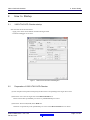
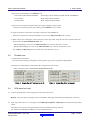
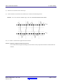
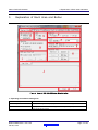
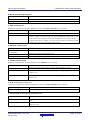
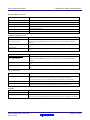
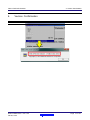
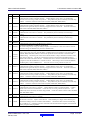
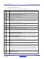
V850 JTAG OCD Checker
User’s Manual
Supported Devices:
V850 Family
All information contained in these materials, including products and product specifications,
represents information on the product at the time of publication and is subject to change by
Renesas Electronics Corp. without notice. Please review the latest information published by
Renesas Electronics Corp. through various means, including the Renesas Electronics Corp.
website (http://www.renesas.com).
Rev.1.00 Feb 2013
Notice
1.
Descriptions of circuits, software and other related information in this document are provided only to illustrate the operation of
semiconductor products and application examples. You are fully responsible for the incorporation of these circuits, software,
and information in the design of your equipment. Renesas Electronics assumes no responsibility for any losses incurred by you
or third parties arising from the use of these circuits, software, or information.
2.
Renesas Electronics has used reasonable care in preparing the information included in this document, but Renesas Electronics
does not warrant that such information is error free. Renesas Electronics assumes no liability whatsoever for any damages
incurred by you resulting from errors in or omissions from the information included herein.
3.
Renesas Electronics does not assume any liability for infringement of patents, copyrights, or other intellectual property rights of
third parties by or arising from the use of Renesas Electronics products or technical information described in this document. No
license, express, implied or otherwise, is granted hereby under any patents, copyrights or other intellectual property rights of
Renesas Electronics or others.
4.
You should not alter, modify, copy, or otherwise misappropriate any Renesas Electronics product, whether in whole or in part.
Renesas Electronics assumes no responsibility for any losses incurred by you or third parties arising from such alteration,
modification, copy or otherwise misappropriation of Renesas Electronics product.
5.
Renesas Electronics products are classified according to the following two quality grades: “Standard” and “High Quality”. The
recommended applications for each Renesas Electronics product depends on the product’s quality grade, as indicated below.
“Standard”:
Computers; office equipment; communications equipment; test and measurement equipment; audio and visual
equipment; home electronic appliances; machine tools; personal electronic equipment; and industrial robots etc.
“High Quality”: Transportation equipment (automobiles, trains, ships, etc.); traffic control systems; anti-disaster systems; anticrime systems; and safety equipment etc.
Renesas Electronics products are neither intended nor authorized for use in products or systems that may pose a direct threat to
human life or bodily injury (artificial life support devices or systems, surgical implantations etc.), or may cause serious property
damages (nuclear reactor control systems, military equipment etc.). You must check the quality grade of each Renesas
Electronics product before using it in a particular application. You may not use any Renesas Electronics product for any
application for which it is not intended. Renesas Electronics shall not be in any way liable for any damages or losses incurred
by you or third parties arising from the use of any Renesas Electronics product for which the product is not intended by Renesas
Electronics.
6.
You should use the Renesas Electronics products described in this document within the range specified by Renesas Electronics,
especially with respect to the maximum rating, operating supply voltage range, movement power voltage range, heat radiation
characteristics, installation and other product characteristics. Renesas Electronics shall have no liability for malfunctions or
damages arising out of the use of Renesas Electronics products beyond such specified ranges.
7.
Although Renesas Electronics endeavors to improve the quality and reliability of its products, semiconductor products have
specific characteristics such as the occurrence of failure at a certain rate and malfunctions under certain use conditions. Further,
Renesas Electronics products are not subject to radiation resistance design. Please be sure to implement safety measures to
guard them against the possibility of physical injury, and injury or damage caused by fire in the event of the failure of a Renesas
Electronics product, such as safety design for hardware and software including but not limited to redundancy, fire control and
malfunction prevention, appropriate treatment for aging degradation or any other appropriate measures. Because the evaluation
of microcomputer software alone is very difficult, please evaluate the safety of the final products or systems manufactured by
you.
8.
Please contact a Renesas Electronics sales office for details as to environmental matters such as the environmental compatibility
of each Renesas Electronics product. Please use Renesas Electronics products in compliance with all applicable laws and
regulations that regulate the inclusion or use of controlled substances, including without limitation, the EU RoHS Directive.
Renesas Electronics assumes no liability for damages or losses occurring as a result of your noncompliance with applicable laws
and regulations.
9.
Renesas Electronics products and technology may not be used for or incorporated into any products or systems whose
manufacture, use, or sale is prohibited under any applicable domestic or foreign laws or regulations. You should not use
Renesas Electronics products or technology described in this document for any purpose relating to military applications or use
by the military, including but not limited to the development of weapons of mass destruction. When exporting the Renesas
Electronics products or technology described in this document, you should comply with the applicable export control laws and
regulations and follow the procedures required by such laws and regulations.
10. It is the responsibility of the buyer or distributor of Renesas Electronics products, who distributes, disposes of, or otherwise
places the product with a third party, to notify such third party in advance of the contents and conditions set forth in this
document, Renesas Electronics assumes no responsibility for any losses incurred by you or third parties as a result of
unauthorized use of Renesas Electronics products.
11. This document may not be reproduced or duplicated in any form, in whole or in part, without prior written consent of Renesas
Electronics.
12. Please contact a Renesas Electronics sales office if you have any questions regarding the information contained in this document
or Renesas Electronics products, or if you have any other inquiries.
(Note 1) “Renesas Electronics” as used in this document means Renesas Electronics Corporation and also includes its majorityowned subsidiaries.
(Note 2) “Renesas Electronics product(s)” means any product developed or manufactured by or for Renesas Electronics.
(2012.4)
V850 JTAG OCD Checker
Contents
Contents
1.
Overview .........................................................................................................................................................................................4
1.1
Details of tested items ..................................................................................................................................................................................... 4
1.2
Test result ....................................................................................................................................................................................................... 4
1.3
Operating Environment................................................................................................................................................................................... 5
2.
How to Startup ................................................................................................................................................................................. 6
2.1
V850 JTAG OCD Checker startup ................................................................................................................................................................. 6
2.2
Preparation of V850 JTAG OCD Checker ...................................................................................................................................................... 6
2.3
Emulator test ................................................................................................................................................................................................... 7
2.4
DCK wave form test ....................................................................................................................................................................................... 7
3.
Explanation of Each Area and Button .............................................................................................................................................. 9
4.
Version Confirmation ..................................................................................................................................................................... 12
5.
Corrective Actions in Case of NG................................................................................................................................................... 13
5.1
V850 JTAG OCD emulator test .................................................................................................................................................................... 13
5.1.1
When V850 E/V850ES is chosen ..........................................................................................................................................................13
5.1.2
When V850E2M/V850E2S is chosen ....................................................................................................................................................16
6.
Changes from N-Wire Checker V1.30/V2.10 .................................................................................................................................. 19
7.
Restrictions .................................................................................................................................................................................... 20
R20UT2462EJ0100
Feb 20, 2013
Rev.1.00
Page 3 of 23
V850 JTAG OCD Checker
1.
1. Overview
Overview
V850 JTAG OCD Checker is Emulator Utility software for V850 for simply testing the PC-connected OCD emulator
(QB-V850MINI(L) , IE-V850E1-CD-NW, E1 Emulator, E20 Emulator) and the target CPU operation.
1.1
Details of tested items
This section describes the test items that are performed by the V850 JTAG OCD Checker.
♦ Emulator test
OCD Emulator connection, initialization, and target CPU register read/write are checked.
The test results can be output to the log viewer and a log file.
• Connect Test
OCD Emulator is started up and the connection with the target CPU is tested.
• DCU Reg Test
0x00000000, 0xFFFFFFFF, 0x55555555, 0xAAAAAAAA, 0x33333333, and 0xCCCCCCCC are written in that
order to the monitor register in the on-chip debug unit and the values are read to check if they have been
read/written normally.
• CPU Reg Test
A target CPU register read/write test is performed using the monitor program.
(Target CPU registers: r1, r2, r3/sp, r4/gp, r5, r6, r7, r8, r9, r10, r11, r12, r13, r14, r15, r16, r17, r18, r19, r20, r21,
r22, r23, r24, r25, r26, r27, r28, r29, r30/ep, r31/lp, eipc, eipsw, fepc, fepsw, psw, ctpc, ctpsw, dbpc, dbpsw, ctbp,
asid, DIR, BPC0, BPAV0, BPAM0, BPDV0, BPDM0, BPC1, BPAV1,BPAM1, BPDV1, BPDM1, and pc)
Release the security setting using the ID code before accessing a register, if necessary.
• Test All
Connect Test, DCU Reg Test, and CPU Reg Test is performed in that order.
♦ DCK waveform test
The data set from OCD Emulator is output to the DDI signal in order to check the waveform of the DCK signal on the
target system with an oscilloscope.
1.2
Test result
The results of the tests in Emulator Test are output to the log viewer and a log file.
If the test results are NG, refer to
5. Corrective Actions in Case of NG for general causes and corrective actions.
R20UT2462EJ0100
Feb 20, 2013
Rev.1.00
Page 4 of 23
V850 JTAG OCD Checker
1.3
1. Overview
Operating Environment
- Windows XP (Only 32-bit OS)
- Windows Vista (32-bit OS, 64-bit OS)
- Windows 7 (32-bit OS, 64-bit OS)
- Windows 8 (32-bit OS, 64-bit OS)
R20UT2462EJ0100
Feb 20, 2013
Rev.1.00
Page 5 of 23
V850 JTAG OCD Checker
2. How to Setup
2.
How to Startup
2.1
V850 JTAG OCD Checker startup
Start the V850 JTAG OCD Checker.
- Apply power to the OCD emulator and then the target board.
- Terminate Debugger if it is active.
Figure 1. V850 JTAG OCD Checker Main Dialog Box
2.2
Preparation of V850 JTAG OCD Checker
(1) Click the [Device file] button and specify the device file corresponding to the target device used.
(2) Select the core series for target CPU in the Microcontroller area.
Please choose either [V850E/ES] core series or [V880E2M/E2S] core series.
(3) Select the JTAG Clock(DCK) in the DCK area.
Selection is required only when [V850E/ES] core series in the Microcontroller area is chosen.
R20UT2462EJ0100
Feb 20, 2013
Rev.1.00
Page 6 of 23
V850 JTAG OCD Checker
2. How to Setup
(4) Select the OCD Emulator in the Emulator area.
• IE-V850E1-CD-NW/QB-V850MINI
: When using with IE-V850E1-CD-NW and QB-V850MINI(L)
• E1 Emulator
: When using with E1 Emulator
• E20 Emulator
: When using with E20 Emulator
(5) Please choose from OCD Emulator the power supply supplied to target system.
Selection is required only when [E1 Emulator] in the Emulator area is chosen.
(6) Input the frequency of the main clock input to the device in the Clock area.
Selection is required only when [V850E/ES] core series in the Microcontroller area is chosen.
(7) When using a device having the security function in single-chip mode, check the “ID code” checkbox and input
the ID code in the Internal ROM Security area.
When [V850E/ES] core series in the Microcontroller area is chosen: ID code is 10 bytes
When [V850E2M/E2S] core series in the Microcontroller area is chosen: ID code is 12 bytes
The Connect and DCU Reg tests are possible even if the ID code is not set.
2.3
Emulator test
(1) Click the [Test All] button.
Each item can be tested by clicking the [Connect], [DCU reg], or [CPU reg] button independently.
(2) When the test has finished, confirm that OK is displayed for each test item.
If NG is displayed, refer to 5 Corrective Actions in Case of NG.
Figure 2. Display When All Test Results are OK
2.4
Figure 3. Display When Error Is Detected
DCK wave form test
(1) Connect the DCK signal of the target board to the oscilloscope probe.
Remark Switch off the power supply of the OCD emulator and target system before performing this connection.
(2) Input 4-byte data (0xcccccccc at shipment) in the DDI output signal for oscilloscope area and then click the [Start]
button.
This function can be used, when [V850 E/ES] is chosen in [Microcontroller] area and
[IE-V850E1-CD-NW/QB-V850MINI] is chosen in [Emulator] area.
R20UT2462EJ0100
Feb 20, 2013
Rev.1.00
Page 7 of 23
V850 JTAG OCD Checker
2. How to Setup
(3) Monitor the waveform on the oscilloscope.
(4) Check whether the waveform noise (reflection) is within the standard range below.
Remark If it is not within the standard range, refer to 5. Corrective Actions in Case of NG.
VOH
VOL
VOH, VOL: Refer to the data sheet supplied with the emulator.
Caution The data is output from the lowermost bit.
Even if data from the target board changes, the same data is always output because data is shifted inside the
emulator.
R20UT2462EJ0100
Feb 20, 2013
Rev.1.00
Page 8 of 23
V850 JTAG OCD Checker
3.
3. Explanetion of Each Area and Button
Explanation of Each Area and Button
Figure 4. Areas in V850 JTAG OCD Checker Main Dialog Box
A. Operating environment setting area
Object
Function
[Device file] button
Displays the dialog box for specifying the device file name of the target CPU.
Text area
Displays the device file name of the target CPU and its path.
JTAG OCD Checker startup.
R20UT2462EJ0100
Feb 20, 2013
Rev.1.00
Specify this at V850
Page 9 of 23
V850 JTAG OCD Checker
3. Explanetion of Each Area and Button
B. Microcontroller selecting area
Object
Function
V850E/ES
Select this item when V850E/ES core series is used.
V850E2M/E2S
Select this item when V850E2M/E2S core series is used.
C. DCK selecting area
(Selection is required only when [V850E/ES] core series in the Microcontroller area is chosen.)
Object
Function
20MHz
Select this item when DCK = 20 MHz is set via the debugger.
10MHz
Select this item when DCK = 10 MHz is set via the debugger.
(“DCK = 10 MHz” is the setting for the case where the V850 JTAG OCD Checker is used
for the self-check board (supplied with the QB-V850MINI(L)) or for a device that does
not operate unless DCK = 10 MHz, or for cases where the operation is unstable with DCK
= 20 MHz, like when a long (2 m) N-Wire cable is used.)
D. Emulator selecting area
Object
Function
IE-V850E1-CD-NW/
QB-V850MINI
E1 Emulator
Select this item when the IE-V850E1-CD-NW or QB-V850MINI(L) is used.
E20 Emulator
Select this item when the E20 Emulator is used.
Select this item when the E1 Emulator is used.
E. Vdd Out selecting area
(Selection is required only when [E1 Emulator] in the Emulator area is chosen.)
Object
Function
Disable
Select this item when the IE-V850E1-CD-NW or QB-V850MINI(L) is used.
3.3V Out
Select this item when from OCD Emulator the power supply supplied to target
system.(3.3V)
Select this item when from OCD Emulator the power supply supplied to target
5V Out
system.(5V)
F. Main clock frequency setting area
(Selection is required only when [V850E/ES] core series in the Microcontroller area is chosen.)
Object
Function
Frequency setting area
Input the frequency of the main clock input to the device.
G. Internal ROM Security ID code specification area
Object
Function
ID code setting box
Check the check box when a device with the security function is used in the single-chip
mode.
Input an ID code when a product device with the security function is used in the
single-chip mode.
ID code setting area
R20UT2462EJ0100
Feb 20, 2013
Rev.1.00
Page 10 of 23
V850 JTAG OCD Checker
3. Explanetion of Each Area and Button
H. OCD emulator test area
Object
Function
[Test All] button
Executes Connect, DCR Reg, and CPU Reg tests in sequence.
[Pause] button
[Stop] button
[Connect] button
Pauses the test. (Testing resumes when this button is clicked again.)
Stops the test.
Starts up the N-Wire emulator, opens communication with the target, and executes
testing for initialization.
Performs testing for DCU register read/write.
Performs testing for CPU register read/write.
[DCU Reg] button
[CPU Reg] button
I. DCK waveform test area
Object
Function
Sets the data of the DDI signal output from the OCD emulator.
When a value of 0xffffffff or greater is set, an error occurs when the [Start] button is
pressed.
Outputs the value (0 to 0xffffffff) specified in the DDI output signal for oscilloscope text
area.
Stops the signal for value testing specified in the DDI output signal for oscilloscope text
area.
DDI output signal
for oscilloscope area
[Start] button
[Stop] button
J. Log viewer area
Object
Function
[Log file] button
Displays the dialog box for specifying the test result log file name.
The log file is overwritten when the V850 JTAG OCD Checker is started up.
A log file is created in the current folder when the file path name is not specified.
Displays the log file name and its path.
Displays the test results as a log (up to approx. 21,000 characters).
The same contents are output to the log file specified in the log file text area.
Text area
Log viewer area
K. Other
Object
[Exit] button
[Clear] button
R20UT2462EJ0100
Feb 20, 2013
Function
Terminates V850 JTAG OCD Checker.
Clears the log viewer display.
If a log file name is specified in the log file text area, the log file contents are not cleared.
Rev.1.00
Page 11 of 23
V850 JTAG OCD Checker
4.
4. Version Confirmation
Version Confirmation
Select the “V850 JTAG OCD Checker version information” menu on the system menu.
R20UT2462EJ0100
Feb 20, 2013
Rev.1.00
Page 12 of 23
V850 JTAG OCD Checker
5. Corrective Actions in Case of NG
5.
Corrective Actions in Case of NG
5.1
V850 JTAG OCD emulator test
The corrective actions for errors and corresponding error numbers are shown below.
Note that errors may occur due to causes other than those below.
5.1.1
Note
When V850 E/V850ES is chosen
*1: Selection is required only when [E1 Emulator] in the Emulator area is chosen.
Italic font: Selection is required only when [IE-V850E1-CD-NW/QB-V850MINI] in the Emulator area is chosen.
No.
Error No.
Error Messages and Corrective Action
1
0x0100
[Driver couldn't be opened.]
The PC and Emulator may be not connected. The PC may be not able to recognize after it has entered
suspend mode, so restart the PC. The device driver may be not installed. Install the driver.
2
0x0105
[Failed in reading device file (dxxxx.800).]
The necessary file may be damaged. Reinstall the device file.
3
0x0109
[USB access failed.]
Exit this utility and re-connect up Emulator.
4
0x010a
0x01a6
[EXEC already work.]
Exit the debugger.
5
0x01a0
[Processing of a monitor was not completed to within a time.]
Confirm that the resonator oscillates normally. Confirm that the correct value is set to MainOSC.
Check the noise level using a DCK waveform test. The problem may also be caused by an internal chip
problem. Check the connection of the N-Wire I/F(DCK, DMS, DDI, DDO, DRST).
6
0x03a0
[The Power supply of target is OFF.]
Check the target power supply. Check the cable connecting the Emulator and target board.
that the VDD signal is input to the connector of the target board.
7
0x0400
[Incorrect value of MainOSC.]
MainOSC can't be set to 0.
8
0x0B04
[Although the power supply of target is ON, Vdd Out is set Enable.] (*1)
Set Vdd Out as Disable, or shut off the power supply of the target.
0x0c01
[During access of register, CPU did timeout.]
Confirm that the resonator oscillates normally. Confirm that the correct value is set to MainOSC.
Check the noise level using a DCK waveform test. The problem may also be caused by an internal chip
problem. Check the connection of the N-Wire I/F(DCK, DMS, DDI, DDO, DRST).
0x0c02
[During access of memory, CPU did timeout.]
Confirm that the resonator oscillates normally. Confirm that the correct value is set to MainOSC.
Check the noise level using a DCK waveform test. The problem may also be caused by an internal chip
problem. Check the connection of the N-Wire I/F(DCK, DMS, DDI, DDO, DRST).
0x0c03
[During access of I/O register, CPU did timeout.]
Confirm that the resonator oscillates normally. Confirm that the correct value is set to MainOSC.
Check the noise level using a DCK waveform test. The problem may also be caused by an internal chip
problem. Check the connection of the N-Wire I/F(DCK, DMS, DDI, DDO, DRST).
9
10
11
R20UT2462EJ0100
Feb 20, 2013
Rev.1.00
Check
Page 13 of 23
V850 JTAG OCD Checker
No.
Error No.
5. Corrective Actions in Case of NG
Error Messages and Corrective Action
0x0c23
[Bus hold under continuation.]
Confirm that the resonator oscillates normally. Confirm that the correct value is set to MainOSC.
Check the noise level using a DCK waveform test. The problem may also be caused by an internal chip
problem. Check the connection of the N-Wire I/F(DCK, DMS, DDI, DDO, DRST).
13
0x0c24
[It couldn't shift to debug mode.]
Confirm that the resonator oscillates normally. Confirm that the correct value is set to MainOSC.
Check the clock signal. This may be caused by a stopped clock or a slow clock. Check the connection
of the N-Wire I/F(DCK, DMS, DDI, DDO, DRST).
14
0x0c2e
[During access of flash memory information, CPU did timeout.]
Confirm that the correct device is selected. The problem may also be caused by an internal chip
problem.
15
0x0c2f
[During access of flash memory information, the response from CPU was not right.]
Confirm that the correct device is selected. The problem may also be caused by an internal chip
problem.
16
0x0c35
[IRAM cannot be accessed.]
Confirm that the correct device file(IRAM size) is selected.
17
0x0c43
[Connection of Emulator couldn't be performed.]
The switch setting may be wrong if a desktop computer is used and two or more PC cards are inserted.
Check the setting. The Emulator may also have malfunctioned.
0x0c70
0x0c76
0x0c77
[It has not accessed to DCU.]
A DCU access error may occur when the DCK = 20 MHz setting is selected due to noise in the N-Wire
I/F(DCK, DMS, DDI, DDO, DRST) or because the specification is not satisfied, so select the DCK =
10 MHz setting. Check the power to the device and the interface voltage. Check the connection of the
signal lines (N-Wire I/F). The device executes the program in user mode until the [Start] button is
clicked in the V850 JTAG OCD Checker. Therefore, the device cannot be connected to the Emulator if
a program to clear the OCDM0 bit to 0 is under execution. When using a device with the OCDM0 bit
(OCDM register), set the OCDM0 bit to 1. Check the noise level using a DCK waveform test.
12
18
19
0x0c71
20
0x0c72
[Reset couldn't be performed.]
Confirm that the resonator oscillates normally. Confirm that the correct value is set to MainOSC.
Check the clock signal. This may be caused by a stopped clock or a slow clock. Check the connection
of the N-Wire I/F(DCK, DMS, DDI, DDO, DRST).
[Monitor memory couldn't be accessed.]
Confirm that the resonator oscillates normally. Confirm that the correct value is set to MainOSC.
Check the noise level using a DCK waveform test. The problem may also be caused by an internal chip
problem. Check the connection of the N-Wire I/F(DCK, DMS, DDI, DDO, DRST).
0x0c73
[Monitor execution couldn't be performed.]
Confirm that the resonator oscillates normally. Confirm that the correct value is set to MainOSC.
Check the noise level using a DCK waveform test. The problem may also be caused by an internal chip
problem. Check the connection of the N-Wire I/F(DCK, DMS, DDI, DDO, DRST).
22
0x0c74
[CPU register cannot be accessed.]
Confirm that the correct device is selected. Confirm that the resonator oscillates normally. Confirm
that the correct value is set to MainOSC. Check the noise level using a DCK waveform test. The
problem may also be caused by an internal chip problem. Check the connection of the N-Wire I/F(DCK,
DMS, DDI, DDO, DRST).
23
0x0ca2
0x0ca3
[Incorrect selection of a device file]
Confirm that the correct device is selected.
0xf603
[Incorrect ID Code.]
The ID code is incorrect. Input a correct ID code. If the FLMD0 pin is High, confirm that the pin is
connected according to the user’s manual of the Emulator. Check the N-Wire connection enable flag
(bit 7 at address 79). If this flag cannot be connected or the ID code has been forgotten, erase the flash
memory using the flash programmer.
21
24
R20UT2462EJ0100
Feb 20, 2013
Rev.1.00
Page 14 of 23
V850 JTAG OCD Checker
No.
Error No.
5. Corrective Actions in Case of NG
Error Messages and Corrective Action
25
0xf604
[Incorrect ID Code. Abort the V850 JTAG OCD Checker.]
The ID code is incorrect. Re-start the V850 JTAG OCD Checker and input a correct ID code. If the
FLMD0 pin is High, confirm that the pin is connected according to the user’s manual of the Emulator.
Check the N-Wire connection enable flag (bit 7 at address 79). If this flag cannot be connected or the ID
code has been forgotten, erase the flash memory using the flash programmer.
26
0xf605
[The ID code input setup is required.]
Check the ID code check box and input the ID code.
27
0xf606
[IECUBE is connected.]
Remove IECUBE.
R20UT2462EJ0100
Feb 20, 2013
Rev.1.00
Page 15 of 23
V850 JTAG OCD Checker
5.1.2
Note
5. Corrective Actions in Case of NG
When V850E2M/V850E2S is chosen
*1: Selection is required only when [E1 Emulator] in the Emulator area is chosen.
No.
Error No.
1
0x0100
[Driver couldn't be opened.]
The PC and Emulator may be not connected. The PC may be not recognized after it has entered
suspend mode, so restart the PC. The device driver may be not installed. Install the driver.
2
0x0105
[Failed in reading device file (dxxxx.800).]
The necessary file may be damaged. Reinstall the device file.
3
0x0109
[USB access failed.]
Exit this utility and re-connect up Emulator.
4
0x010a
0x01a6
[EXEC already work.]
Exit the debugger.
5
0x01a0
[Processing of a monitor was not completed to within a time.]
Confirm that the resonator oscillates normally. Confirm that the correct value is set to MainOSC.
The problem may also be caused by an internal chip problem. Check the connection of the NEXUS
I/F(TCK, TMS, TDI, TDO, TRST, RDY).
6
0x03a0
[The Power supply of target is OFF.]
Check the target power supply. Check the cable connecting the Emulator and target board.
that the VDD signal is input to the connector of the target board.
7
0x0400
[Incorrect value of MainOSC.]
MainOSC can't be set to 0.
8
0x0B04
[Although the power supply of target is ON, Vdd Out is set Enable.] (*1)
Set Vdd Out as Disable, or shut off the power supply of the target.
0x0c01
[During access of register, CPU did timeout.]
Confirm that the resonator oscillates normally. Confirm that the correct value is set to MainOSC.
The problem may also be caused by an internal chip problem. Check the connection of the NEXUS
I/F(TCK, TMS, TDI, TDO, TRST, RDY).
0x0c02
[During access of memory, CPU did timeout.]
Confirm that the resonator oscillates normally. Confirm that the correct value is set to MainOSC.
The problem may also be caused by an internal chip problem. Check the connection of the NEXUS
I/F(TCK, TMS, TDI, TDO, TRST, RDY).
11
0x0c24
[It couldn't shift to debug mode.]
Confirm that the resonator oscillates normally. Confirm that the correct value is set to MainOSC.
Check the clock signal. This may be caused by a stopped clock or a slow clock. Check the connection
of the NEXUS I/F(TCK, TMS, TDI, TDO, TRST, RDY).
12
0x0c2e
[During access of flash memory information, CPU did timeout.]
Confirm that the correct device is selected. The problem may also be caused by an internal chip
problem.
13
0x0c2f
14
0x0c43
15
0x0c70
0x0c77
9
10
Error Messages and Corrective Action
Check
[During access of flash memory information, the response from CPU was not right.]
Confirm that the correct device is selected. The problem may also be caused by an internal chip
problem.
[Connection of Emulator couldn't be performed.]
Confirm that the resonator oscillates normally. Check the OPJTAG bit of OPBT0. If OPJTAG bit is set to
1 (JTAG I/F is enable), Emulator can connect to the device. Confirm the RESET circuit on the target
board. It might have been unable to shift to a debug mode, because the device was during RESET. Set the
OPBT0 to stop the Watchdog timer using the flash programmer. It might have been unable to shift to a
debug mode, because often generating RESET by the Watchdog timer. The Emulator may also have
malfunctioned.
[It has not accessed to DCU.]
Check the power to the device and the interface voltage. Check the connection of the NEXUS I/F(TCK,
TMS, TDI, TDO, TRST, RDY).
R20UT2462EJ0100
Feb 20, 2013
Rev.1.00
Page 16 of 23
V850 JTAG OCD Checker
No.
Error No.
16
0x0c71
17
0x0c72
5. Corrective Actions in Case of NG
Error Messages and Corrective Action
[Reset couldn't be performed.]
Confirm that the resonator oscillates normally. Confirm that the correct value is set to MainOSC.
Check the clock signal. This may be caused by a stopped clock or a slow clock. Check the connection
of the NEXUS I/F(TCK, TMS, TDI, TDO, TRST, RDY).
[Monitor memory couldn't be accessed.]
Confirm that the resonator oscillates normally. Confirm that the correct value is set to MainOSC.
The problem may also be caused by an internal chip problem. Check the connection of the NEXUS
I/F(TCK, TMS, TDI, TDO, TRST, RDY).
0x0c73
[Monitor execution couldn't be performed.]
Confirm that the resonator oscillates normally. Confirm that the correct value is set to MainOSC.
The problem may also be caused by an internal chip problem. Check the connection of the NEXUS
I/F(TCK, TMS, TDI, TDO, TRST, RDY).
19
0x0c74
[CPU register cannot be accessed.]
Confirm that the correct device is selected. Confirm that the resonator oscillates normally. Confirm
that the correct value is set to MainOSC. The problem may also be caused by an internal chip problem.
Check the connection of the NEXUS I/F(TCK, TMS, TDI, TDO, TRST, RDY).
20
0x0ca3
[Incorrect selection of a device file]
Confirm that the correct device is selected.
0xf603
[Incorrect ID Code.]
The ID code is incorrect. Input a correct ID code. If the FLMD0 pin is High, confirm that the pin is
connected according to the user’s manual of the Emulator. Check the On-chip Debug enable flag (bit 7
at address 79). If this flag is set to disable or the ID code has been forgotten, erase the flash memory
using the flash programmer.
22
0xf604
[Incorrect ID Code. Abort the V850 JTAG OCD Checker.]
The ID code is incorrect. Re-start the V850 JTAG OCD Checker and input a correct ID code. If the
FLMD0 pin is High, confirm that the pin is connected according to the user’s manual of the Emulator.
Check the On-chip Debug enable flag (bit 7 at address 79). If this flag is set to disable or the ID code
has been forgotten, erase the flash memory using the flash programmer.
23
0xf605
[The ID code input setup is required.]
Check the ID code check box and input the ID code.
24
0xf606
[IECUBE is connected.]
Remove IECUBE.
18
21
R20UT2462EJ0100
Feb 20, 2013
Rev.1.00
Page 17 of 23
V850 JTAG OCD Checker
If data access by
5. Corrective Actions in Case of NG
[DCU Reg] test results in NG
Normal access to the DCU register is impossible.
Perform a DCK waveform test.
If no anomaly is found with the DCK waveform test, the register may be damaged, so try again with a different chip.
If data access by
[CPU Reg] test results in NG
Normal access to the CPU register is impossible.
Perform a DCK waveform test.
If no anomaly is found with the DCK waveform test, the register may be damaged, so try again with a different chip.
5.2
DCK waveform test
Check the following items regarding the design of the target board, in accordance with the user's Manual.
CHAPTER 4 NOTES ON TARGET SYSTEM DESIGN in the IE-V850E1-CD-NW User’s Manual or 3.4
Designing Target System Circuits in the QB-V850MINI(L) User's Manual.
IE-V850E1-CD-NW/QB-V850MINI
• Is the pattern of the N-Wire interface signal 100 mm or less?
• Is the DCK signal shielded by a pull-up resistorNote + GND?
• Is a pull-up resistorNote connected to the DMS, DDI, and DDO signals?
• Is a pull-down resistorNote connected to the _DRSTZ signal (or DRST signal)?
Note The resistance of the resistor must be as specified for each device.
pull-up/down resistors.
Some devices have on-chip
With these devices, an external resistor is not necessary.
Also check the following items regarding the power supply capacity of the target board.
• Is a power supply with a sufficient capacity used?
• Are sufficient capacitors provided on the target board?
• Is a bypass capacitor connected to all the power supply pins of the CPU?
• Is the GND plane on the target board sufficiently large?
R20UT2462EJ0100
Feb 20, 2013
Rev.1.00
Page 18 of 23
V850 JTAG OCD Checker
6.
6. Changes from N-Wire Checker V1.30/V2.10
Changes from N-Wire Checker V1.30/V2.10
The following point has been changed from N-Wire Checker V1.30 and V2.10 to V850 JTAG OCD Checker V1.00.
• The V850E2M core and V850E2S core are now supported.
• The E1 Emulator and E20 Emulator are now supported.
R20UT2462EJ0100
Feb 20, 2013
Rev.1.00
Page 19 of 23
V850 JTAG OCD Checker
7.
7. Restrictions
Restrictions
• Up to 21,000 characters can be displayed in the log viewer area.
• If the number of characters exceeds the displayable limit, the oldest data will be overwritten.
In this case, refer to the
log file as all the data is recorded there.
• In cases when there is a severe shortage of system resources, output to the log viewer area will stop.
In this case, even
though screen output has stopped, data will continue to be recorded in the log file and can be referenced from there.
(The log file is overwritten when the V850 JTAG OCD Checker is started up.)
R20UT2462EJ0100
Feb 20, 2013
Rev.1.00
Page 20 of 23
V850 JTAG OCD Checker
User's Manual
Publication Date:
Feb 20, 2013
Rev.1.00
Published by:
Renesas Electronics Corporation
http://www.renesas.com
SALES OFFICES
Refer to "http://www.renesas.com/" for the latest and detailed information.
Renesas Electronics America Inc.
2880 Scott Boulevard Santa Clara, CA 95050-2554, U.S.A.
Tel: +1-408-588-6000, Fax: +1-408-588-6130
Renesas Electronics Canada Limited
1101 Nicholson Road, Newmarket, Ontario L3Y 9C3, Canada
Tel: +1-905-898-5441, Fax: +1-905-898-3220
Renesas Electronics Europe Limited
Dukes Meadow, Millboard Road, Bourne End, Buckinghamshire, SL8 5FH, U.K
Tel: +44-1628-651-700, Fax: +44-1628-651-804
Renesas Electronics Europe GmbH
Arcadiastrasse 10, 40472 Düsseldorf, Germany
Tel: +49-211-65030, Fax: +49-211-6503-1327
Renesas Electronics (China) Co., Ltd.
7th Floor, Quantum Plaza, No.27 ZhiChunLu Haidian District, Beijing 100083, P.R.China
Tel: +86-10-8235-1155, Fax: +86-10-8235-7679
Renesas Electronics (Shanghai) Co., Ltd.
Unit 204, 205, AZIA Center, No.1233 Lujiazui Ring Rd., Pudong District, Shanghai 200120, China
Tel: +86-21-5877-1818, Fax: +86-21-6887-7858 / -7898
Renesas Electronics Hong Kong Limited
Unit 1601-1613, 16/F., Tower 2, Grand Century Place, 193 Prince Edward Road West, Mongkok, Kowloon, Hong Kong
Tel: +852-2886-9318, Fax: +852 2886-9022/9044
Renesas Electronics Taiwan Co., Ltd.
13F, No. 363, Fu Shing North Road, Taipei, Taiwan
Tel: +886-2-8175-9600, Fax: +886 2-8175-9670
Renesas Electronics Singapore Pte. Ltd.
80 Bendemeer Road, Unit #06-02 Hyflux Innovation Centre Singapore 339949
Tel: +65-6213-0200, Fax: +65-6213-0300
Renesas Electronics Malaysia Sdn.Bhd.
Unit 906, Block B, Menara Amcorp, Amcorp Trade Centre, No. 18, Jln Persiaran Barat, 46050 Petaling Jaya, Selangor Darul Ehsan, Malaysia
Tel: +60-3-7955-9390, Fax: +60-3-7955-9510
Renesas Electronics Korea Co., Ltd.
11F., Samik Lavied' or Bldg., 720-2 Yeoksam-Dong, Kangnam-Ku, Seoul 135-080, Korea
Tel: +82-2-558-3737, Fax: +82-2-558-5141
© 2012 Renesas Electronics Corporation. All rights reserved.
Colophon 1.3
© 2012 Renesas Electronics Corporation and Renesas Solutions Corp.
Colophon 1.3
V850 JTAG OCD Checker
User’s Manual
R20UT2462EJ0100