1
To our customers,
Old Company Name in Catalogs and Other Documents
On April 1st, 2010, NEC Electronics Corporation merged with Renesas Technology
Corporation, and Renesas Electronics Corporation took over all the business of both
companies. Therefore, although the old company name remains in this document, it is a valid
Renesas Electronics document. We appreciate your understanding.
Renesas Electronics website: http://www.renesas.com
April 1st, 2010
Renesas Electronics Corporation
Issued by: Renesas Electronics Corporation (http://www.renesas.com)
Send any inquiries to http://www.renesas.com/inquiry.
Notice
1.
2.
3.
4.
5.
6.
7.
All information included in this document is current as of the date this document is issued. Such information, however, is
subject to change without any prior notice. Before purchasing or using any Renesas Electronics products listed herein, please
confirm the latest product information with a Renesas Electronics sales office. Also, please pay regular and careful attention to
additional and different information to be disclosed by Renesas Electronics such as that disclosed through our website.
Renesas Electronics does not assume any liability for infringement of patents, copyrights, or other intellectual property rights
of third parties by or arising from the use of Renesas Electronics products or technical information described in this document.
No license, express, implied or otherwise, is granted hereby under any patents, copyrights or other intellectual property rights
of Renesas Electronics or others.
You should not alter, modify, copy, or otherwise misappropriate any Renesas Electronics product, whether in whole or in part.
Descriptions of circuits, software and other related information in this document are provided only to illustrate the operation of
semiconductor products and application examples. You are fully responsible for the incorporation of these circuits, software,
and information in the design of your equipment. Renesas Electronics assumes no responsibility for any losses incurred by
you or third parties arising from the use of these circuits, software, or information.
When exporting the products or technology described in this document, you should comply with the applicable export control
laws and regulations and follow the procedures required by such laws and regulations. You should not use Renesas
Electronics products or the technology described in this document for any purpose relating to military applications or use by
the military, including but not limited to the development of weapons of mass destruction. Renesas Electronics products and
technology may not be used for or incorporated into any products or systems whose manufacture, use, or sale is prohibited
under any applicable domestic or foreign laws or regulations.
Renesas Electronics has used reasonable care in preparing the information included in this document, but Renesas Electronics
does not warrant that such information is error free. Renesas Electronics assumes no liability whatsoever for any damages
incurred by you resulting from errors in or omissions from the information included herein.
Renesas Electronics products are classified according to the following three quality grades: “Standard”, “High Quality”, and
“Specific”. The recommended applications for each Renesas Electronics product depends on the product’s quality grade, as
indicated below. You must check the quality grade of each Renesas Electronics product before using it in a particular
application. You may not use any Renesas Electronics product for any application categorized as “Specific” without the prior
written consent of Renesas Electronics. Further, you may not use any Renesas Electronics product for any application for
which it is not intended without the prior written consent of Renesas Electronics. Renesas Electronics shall not be in any way
liable for any damages or losses incurred by you or third parties arising from the use of any Renesas Electronics product for an
application categorized as “Specific” or for which the product is not intended where you have failed to obtain the prior written
consent of Renesas Electronics. The quality grade of each Renesas Electronics product is “Standard” unless otherwise
expressly specified in a Renesas Electronics data sheets or data books, etc.
“Standard”:
8.
9.
10.
11.
12.
Computers; office equipment; communications equipment; test and measurement equipment; audio and visual
equipment; home electronic appliances; machine tools; personal electronic equipment; and industrial robots.
“High Quality”: Transportation equipment (automobiles, trains, ships, etc.); traffic control systems; anti-disaster systems; anticrime systems; safety equipment; and medical equipment not specifically designed for life support.
“Specific”:
Aircraft; aerospace equipment; submersible repeaters; nuclear reactor control systems; medical equipment or
systems for life support (e.g. artificial life support devices or systems), surgical implantations, or healthcare
intervention (e.g. excision, etc.), and any other applications or purposes that pose a direct threat to human life.
You should use the Renesas Electronics products described in this document within the range specified by Renesas Electronics,
especially with respect to the maximum rating, operating supply voltage range, movement power voltage range, heat radiation
characteristics, installation and other product characteristics. Renesas Electronics shall have no liability for malfunctions or
damages arising out of the use of Renesas Electronics products beyond such specified ranges.
Although Renesas Electronics endeavors to improve the quality and reliability of its products, semiconductor products have
specific characteristics such as the occurrence of failure at a certain rate and malfunctions under certain use conditions. Further,
Renesas Electronics products are not subject to radiation resistance design. Please be sure to implement safety measures to
guard them against the possibility of physical injury, and injury or damage caused by fire in the event of the failure of a
Renesas Electronics product, such as safety design for hardware and software including but not limited to redundancy, fire
control and malfunction prevention, appropriate treatment for aging degradation or any other appropriate measures. Because
the evaluation of microcomputer software alone is very difficult, please evaluate the safety of the final products or system
manufactured by you.
Please contact a Renesas Electronics sales office for details as to environmental matters such as the environmental
compatibility of each Renesas Electronics product. Please use Renesas Electronics products in compliance with all applicable
laws and regulations that regulate the inclusion or use of controlled substances, including without limitation, the EU RoHS
Directive. Renesas Electronics assumes no liability for damages or losses occurring as a result of your noncompliance with
applicable laws and regulations.
This document may not be reproduced or duplicated, in any form, in whole or in part, without prior written consent of Renesas
Electronics.
Please contact a Renesas Electronics sales office if you have any questions regarding the information contained in this
document or Renesas Electronics products, or if you have any other inquiries.
(Note 1) “Renesas Electronics” as used in this document means Renesas Electronics Corporation and also includes its majorityowned subsidiaries.
(Note 2) “Renesas Electronics product(s)” means any product developed or manufactured by or for Renesas Electronics.
APPLICATION NOTE
M32C/80 Series
Using DMACII (Chained Transfer)
1.
Abstract
This application note describes how to use DMACII in chained transfer.
2.
Introduction
The explanation of this issue is applied to the following condition:
Applicable MCU: M32C/80 Series
This program can also be used when operating other microcomputers within the M16C family, provided they
have DMACII function. However, some functions may have been modified.
Refer to the User’s Manual for details. Use functions covered in this Application Note only after careful
evaluation.
3.
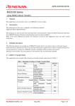
Detailed description
The following explains an example use of DMACII transfer for the case where each time an interrupt request
which has had its priority level set to 7 occurs, data is transferred from memory to memory by a DMACII
transfer and when a specified number of transfers has finished, the transfer mode, transfer count, source of
transfer address, and destination of transfer address are changed.
Figure 1 shows a typical operation of a chained transfer mode.
REJ05B0640-0100/Rev.1.00
May 2005
Page 1 of 11
M32C/80 Series
Using DMACII (Chained Transfer)
Typical operation of a chain transfer in cases where the INT0 interrupt is used as the cause of DMACII
(2) When first DMACII request (INT0 interrupt) occurs
0086h MOD
400h
0001h COUNT After a DMACII transfer,
the COUNT value is
2001h SADR
decremented by 1.
2800h DADR
0800h CADR0 Furthermore, if the source
0000h CADR1 of transfer and the
(1) When initialized
400h
0086h
0002h
2000h
2800h
0800h
0000h
MOD
0086h
0002h
3000h
3800h
0C00h
0000h
MOD
COUNT
SADR
DADR
CADR0
CADR1
destination of transfer are
800h
2000h
2001h
XXh
3000h
3001h
FFh
EEh
3800h
XXh
INT0 interrupt vector (28th entry
COUNT
SADR
DADR
CADR0
CADR1
At the start of a DMACII
transfer, the DMACII
11h
22h
2800h
800h
index located at the
address 0400h
determines the
operation of the transfer
performed.
0400h
2000h
2001h
11h
22h
2800h
11h
3000h
3001h
FFh
EEh
3800h
XXh
INT0 interrupt vector (28th entry
of a relocatable vector table)
0086h
0002h
3000h
3800h
0C00h
0000h
MOD
variable, the SADR and
COUNT
SADR
DADR
CADR0
CADR1
DADR values are
incremented by 1 for 8-bit
transfers or incremented by
2 for 16-bit transfers.
DMACII
transfer
0400h
of a relocatable vector table)
(4) When third DMACII request (INT0 interrupt) occurs
(3) When second DMACII request (INT0 interrupt) occurs
400h
800h
0086h
0000h
2002h
2800h
0800h
0000h
0086h
0002h
3000h
3800h
0C00h
0000h
2000h
2001h
11h
22h
2800h
MOD
COUNT
SADR
DADR
CADR0
CADR1
400h
When COUNT reached 0,
the interrupt vector value
for the cause of a DMACII
transfer is rewritten to the
0086h
0000h
2002h
2800h
0800h
0000h
MOD
0086h
0001h
3001h
3800h
0C00h
0000h
MOD
value of CADR1-CADR0.
MOD
800h
COUNT
SADR
DADR
CADR0
CADR1
DMACII
transfer
2000h
2001h
11h
22h
22h
2800h
11h
3000h
3001h
FFh
EEh
3000h
3001h
FFh
EEh
3800h
XXh
3800h
FFh
COUNT
SADR
DADR
CADR0
CADR1
COUNT
SADR
DADR
CADR0
CADR1
DMACII transfer
The DMACII index located
at the address 800h
determines the operation
INT0 interrupt vector (28th entry
of a relocatable vector table)
0800h
INT0 interrupt vector (28th
entry of a relocatable vector
0800h
of the transfer performed.
table)
The above applies to the following settings:
• SIZE bit = “1” (8 bits transfer)
• OPER bit = “0” (without calculation transfer)
• UPDS bit = “1” (transfer source direction: forward address) • BRST bit = “0” (single transfer)
• UPDD bit = “0” (transfer destination direction: fixed address) • NTE bit = “0” (interrupt no used)
Figure 1. Typical Operation of a DMACII Chained Transfer Mode
REJ05B0640-0100/Rev.1.00
May 2005
Page 2 of 11
M32C/80 Series
Using DMACII (Chained Transfer)
3.1 DMAC II Transfer Mode
This application note example offers functions of chained transfer mode shown in Table 1.
Table 1. Selectable Functions in Chained Transfer Mode
Item
Definition
8 bits
Transfer Block
16 bits
Selection
Yes
Immediate data
Data in memory
Fixed address
Source Direction
Forward address
Fixed address
Destination Direction
Forward address
Calculation
Transfer Without Calculation Transfer
Function
Function
With
Calculation
Transfer
Function
Single transfer
Burst Transfer
Burst transfer
Interrupts not used
End-of-Transfer Interrupt
Interrupts used
Transfer Data
Yes
Yes
Yes
Yes
Yes
Yes
3.2 DMAC II Index
When chain transfers are used, the DMACII index has 4 bytes of CADR1–CADR0 (chain transfer addresses)
added. The total number of bytes that comprise the DMACII index is 12 unless end-of-transfer interrupt is
used.
Be sure to create as many DMACII indices as the number of times a chain transfer is to be performed.
The DMAC II index must be located on the RAM area.
Beginning address of DMACII index (BASE)
MOD
Transfer mode
BASE+2
COUNT
Transfer counter
BASE+4
SADR
Transfer source address
DADR
Transfer destination address
BASE+6
BASE+8
CADR0
BASE+10
Chained transfer address
CADR1
Figure 2.DMAC II Index
REJ05B0640-0100/Rev.1.00
May 2005
Page 3 of 11
M32C/80 Series
Using DMACII (Chained Transfer)
3.3 DMAC II Transfer
The interrupt requests from all peripheral functions whose ILVL2–ILVL0 bits in the interrupt control
register have been set to “111b” constitute the cause of requests to DMAC II. In this application note, the
INT0 interrupt is used for the cause of DMAC II request.
3.4 Setting Up the Relocatable Vector Table
The relocatable vector tables must be located on the RAM area.
During a chain transfer, when COUNT (transfer counter) reaches “0”, the peripheral function interrupt
vector that constitutes the cause of a DMACII request changes to the CADR1–CADR0 value of the DMACII
index.
REJ05B0640-0100/Rev.1.00
May 2005
Page 4 of 11
M32C/80 Series
Using DMACII (Chained Transfer)
3.5 Register Setting
To enable the operation defined in "Section 3. Detailed description", the following register settings must be
taken place step by step. For detail configuration of each register, please refer to M32C/80 Series
HARDWARE MANUAL.
(1) Interrupt disable
Set I flag to “0”.
(2) Create a relocatable vector table
Create a relocatable vector table in the RAM.
(3) Interrupt table register
Set the beginning address of the relocatable vector table located in the RAM.
(4) Transfer mode (MOD)
b15
b8 b7
For (4) through (8), create as many DMACII indices as the
b0
0 0 0 0 0 0 0 0 1 0 0 0 0 1 1 0
number of times a chain transfer is to be performed.
SIZE
Transfer Unit Select Bit
0: 8 bits
1: 16 bits
IMM
Transfer Data Select Bit
0: Immediate data
1: Memory
UPDS
Transfer Source Direction Select Bit
0: Fixed address
1: Forward address
UPDD
Transfer Destination Direction Select Bit
0: Fixed address
1: Forward address
OPER
Calculation Transfer Function Select Bit
0: Not used
BRST
Burst Transfer Select Bit
0: Single transfer
INTE
End-of-Transfer Interrupt Select Bit
0: Interrupt not used
CHAIN
Chained Transfer Select Bit
1: Use chained transfer
-
Nothing is assigned.
Set to “0000000b”
MULT
Multiple Transfer Select Bit
0: Multiple transfer not used
(5) Transfer count (COUNT)
b15
b0
16 bits
Set the number of times transferred.
REJ05B0640-0100/Rev.1.00
May 2005
Page 5 of 11
M32C/80 Series
Using DMACII (Chained Transfer)
(6) Transfer source address (SADR)
b15
b0
16 bits
Set the source address of transfer.
(7) Transfer destination address (DADR)
b15
b0
16 bits
Set the destination address of transfer.
When COUNT reaches “0”, the peripheral
function interrupt vector that constitutes the
(8) Chained transfer address (CADR)
b31
b0
cause of a DMACII request changes to the
CADR value.
32 bits
Set the beginning address of the DMACII index to which the transfer is chained.
(9) RLVL register
b7
b0
0 0 1 0 0 *
*
*
RLVL2 to RLVL0
FSIT
Stop/Wait Mode Exit Minimum Interrupt Priority Level Control Bit
High-Speed Interrupt Set Bit
Set to “0”
-
DMAC II and high-speed interrupts cannot be
Nothing is assigned.
used at the same time.
Set to “0”
DMAII
DMAC II Select Bit
Set to “1”
-
Nothing is assigned.
Set to “00b”
(10) Interrupt Control Register
b7
0 0 *
Set all interrupt request registers for the
interrupts to be used as the cause of DMAC II
requests.
b0
* 0 1 1 1
ILVL2 to ILVL0
Interrupt Priority Level Select Bit
Set to “111b”
IR
Set the priority level of the interrupt used as
Interrupt Request Bit
the cause of DMAC II request to 7.
Set to “0”
POL
Polarity Switch Bit (INT0IC to INT5IC)
0: Selects falling edge or “L”
1: Selects rising edge or “H”
LVS
Level Sensitive/Edge Sensitive Switch Bit (INT0IC to INT5IC)
0: Edge sensitive
1: Level sensitive
-
Nothing is assigned.
Set to “00b”
REJ05B0640-0100/Rev.1.00
The POL and LVS bits are accommodated in the INT0ICINT5IC registers. In other interrupt request registers, set it
to “0”.
May 2005
Page 6 of 11
M32C/80 Series
Using DMACII (Chained Transfer)
4.
Example of a Sample Program
4.1 C language source
/****************************************************************************
/* FILENAME: rej05b0640_src.c
*
/* Ver : 1.00
*
/* FUNCTION: DMACII(Chained transfer)
*
/****************************************************************************/
/*******************************/
/*
include file
*/
/*******************************/
#include <stdio.h>
#include <string.h>
#include "sfr32c83.h"
/*******************************/
/*
DMACII
*/
/*******************************/
struct DMACII_INDEX{
union
{
struct{
char
size:1;
/* Transfer Unit Select Bit */
char
imm:1;
/* Transfer Data Select Bit */
char
upds:1;
/* Transfer Source Direction Select Bit */
char
updd:1;
/* Transfer Destination Direction Select Bit */
char
oper:1;
/* Calculation Transfer Function Select Bit */
char
brst:1;
/* Burst Transfer Select Bit */
char
inte:1;
/* End-of-Transfer Interrupt Select Bit */
char
chain:1;
/* Chained Transfer Select Bit */
char
reserve:7;
char
mult:1;
/* Multiple Transfer Select Bit */
}mod_bit;
unsigned short mod_word;
}mod;
unsigned short count;
/* Transfer count */
unsigned char near *sadr;
/* Transfer source address */
char near *dadr;
/* Transfer destination address */
struct DMACII_INDEX far *cadr; /* Chained transfer address */
}dm_index[2];
long ram_vect[64];
/* Relocatable vector table */
/* Transfer data array */
static unsigned char near data1[5] = {0x11,0x22,0x33,0x44,0x55};
static unsigned char near data2[5] = {0xff,0xee,0xdd,0xcc,0xbb};
/* Transfer destination memory
*/
unsigned char near dest1;
unsigned char near dest2;
#define S_VECTOR
((unsigned long*)0xfefd00)
/* Relocatable vector address */
/*******************************/
/*
main
*/
/*******************************/
void main(void){
asm("
fclr
i
");
/* Interrupt disable */
memcpy(ram_vect,S_VECTOR,64*4);
/* Copy relocatable vector to RAM */
asm("
ldc
#_ram_vect, intb
"); /* Set relocatable vector to RAM */
/* DMACII setting */
dm_index[0].mod.mod_word = 0x0086; /* Transfer Unit:
8bit
*/
/* Transfer Data:
Memory */
/* Transfer Source:
Forward */
/* Transfer Destination:Fixed
*/
/* Calculation Transfer:None
*/
/* Burst Transfer
:Single */
/* Interrupt:
None
*/
/* Chained Transfer:
Have
*/
/* Multiple Transfer:
None
*/
dm_index[0].count = 5;
dm_index[0].sadr = data1;
dm_index[0].dadr = &dest1;
dm_index[0].cadr = &dm_index[1];
REJ05B0640-0100/Rev.1.00
/* number of transfer = 5 */
/* Source of transfer = beginning address of the data array
/* Destination of transfer = dest1 */
May 2005
*/
Page 7 of 11
M32C/80 Series
Using DMACII (Chained Transfer)
dm_index[1].mod.mod_word = 0x0006; /* Transfer Unit:
8bit
/* Transfer Data:
Memory */
/* Transfer Source:
Forward */
/* Transfer Destination:Fixed
*/
/* Calculation Transfer:None
*/
/* Burst Transfer
:Single */
/* Interrupt:
None
*/
/* Chained Transfer:
None
*/
/* Multiple Transfer:
None
*/
*/
dm_index[1].count = 5;
/* number of transfer = 5 */
dm_index[1].sadr = data2;
/* Source of transfer = beginning address of the data array */
dm_index[1].dadr = &dest2;
/* Destination of transfer = dest2 */
dm_index[1].cadr = &dm_index[0];
/* Set the interrupt used for DMAC II */
rlvl = 0x20;
/* Interrupt priority level 7 is used for DMAC II transfers */
int0ic = 0x07;
/* INT0 interrupt level 7 (used for DMACII) */
while(1);
}
4.2 Relocatable Vector Tables
;--------------------------------------------------------------; variable vector section
;--------------------------------------------------------------.section vector,ROMDATA
; variable vector table
.org
VECTOR_ADR
.lword
.lword
.lword
.lword
.lword
.lword
.lword
.lword
.lword
dummy_int
dummy_int
dummy_int
dummy_int
dummy_int
dummy_int
dummy_int
dummy_int
dummy_int
;
;
;
;
;
; BRK (software int 0)
;
;
;
;
;
;
;
; DMA0 (software int 8)
(Omission)
.lword
.lword
.lword
.lword
.lword
.glb
.lword
.lword
dummy_int
dummy_int
dummy_int
dummy_int
dummy_int
_dm_index
_dm_index
dummy_int
;
;
;
;
;
REJ05B0640-0100/Rev.1.00
;
;
;
;
;
INT5
INT4
INT3
INT2
INT1
(software
(software
(software
(software
(software
int
int
int
int
int
26)
27)
28)
29)
30)
; INT0 (software int 31)
; TIMER B5 (software int 32)
(Omission)
May 2005
Page 8 of 11
M32C/80 Series
Using DMACII (Chained Transfer)
5.
Reference
Renesas Technology Corporation Home Page
http://www.renesas.com/
E-mail Support
E-mail: [email protected]
Hardware Manual
M32C/80 Group Hardware Manual
(Use the latest version on the home page: http://www.renesas.com)
TECHNICAL UPDATE/TECHNICAL NEWS
(Use the latest information on the home page: http://www.renesas.com)
REJ05B0640-0100/Rev.1.00
May 2005
Page 9 of 11
M32C/80 Series
Using DMACII (Chained Transfer)
REVISION HISTORY
Rev.
Date
1.00
2005.05.20
REJ05B0640-0100/Rev.1.00
Page
-
Description
Summary
First edition issued
May 2005
Page 10 of 11
M32C/80 Series
Using DMACII (Chained Transfer)
Keep safety first in your circuit designs!
Keep safety first in your circuit designs!
Notes regarding these materials
1. Renesas Technology Corporation puts the maximum effort into making semiconductor products
better and more reliable, but there is always the possibility that trouble may occur with them. Trouble
with semiconductors may lead to personal injury, fire or property damage.
Remember to give due consideration to safety when making your circuit designs, with appropriate
measures such as (i) placement of substitutive, auxiliary circuits, (ii) use of nonflammable material or
(iii) prevention against any malfunction or mishap.
Notes regarding these materials
1. These materials are intended as a reference to assist our customers in the selection of the Renesas
Technology Corporation product best suited to the customer's application; they do not convey any
license under any intellectual property rights, or any other rights, belonging to Renesas Technology
Corporation or a third party.
2. Renesas Technology Corporation assumes no responsibility for any damage, or infringement of any
third-party's rights, originating in the use of any product data, diagrams, charts, programs,
algorithms, or circuit application examples contained in these materials.
3. All information contained in these materials, including product data, diagrams, charts, programs and
algorithms represents information on products at the time of publication of these materials, and are
subject to change by Renesas Technology Corporation without notice due to product improvements
or other reasons. It is therefore recommended that customers contact Renesas Technology
Corporation or an authorized Renesas Technology Corporation product distributor for the latest
product information before purchasing a product listed herein.
The information described here may contain technical inaccuracies or typographical errors.
Renesas Technology Corporation assumes no responsibility for any damage, liability, or other loss
rising from these inaccuracies or errors.
Please also pay attention to information published by Renesas Technology Corporation by various
means, including the Renesas Technology Corporation Semiconductor home page
(http://www.renesas.com).
4. When using any or all of the information contained in these materials, including product data,
diagrams, charts, programs, and algorithms, please be sure to evaluate all information as a total
system before making a final decision on the applicability of the information and products. Renesas
Technology Corporation assumes no responsibility for any damage, liability or other loss resulting
from the information contained herein.
5. Renesas Technology Corporation semiconductors are not designed or manufactured for use in a
device or system that is used under circumstances in which human life is potentially at stake.
Please contact Renesas Technology Corporation or an authorized Renesas Technology Corporation
product distributor when considering the use of a product contained herein for any specific
purposes, such as apparatus or systems for transportation, vehicular, medical, aerospace, nuclear,
or undersea repeater use.
6. The prior written approval of Renesas Technology Corporation is necessary to reprint or reproduce
in whole or in part these materials.
7. If these products or technologies are subject to the Japanese export control restrictions, they must
be exported under a license from the Japanese government and cannot be imported into a country
other than the approved destination.
Any diversion or reexport contrary to the export control laws and regulations of Japan and/or the
country of destination is prohibited.
8. Please contact Renesas Technology Corporation for further details on these materials or the
products contained therein.
REJ05B0640-0100/Rev.1.00
May 2005
Page 11 of 11