1
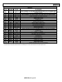
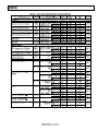
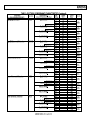
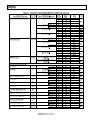
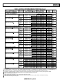
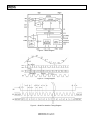
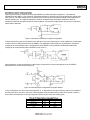
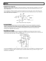
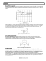
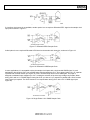
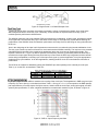
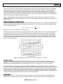
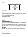
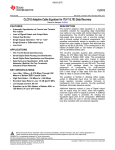
This specification documents the detail requirements for space qualified product manufactured on Analog Devices, Inc.'s QML certified line per MIL-PRF-38535 Level V except as modified herein. The manufacturing flow described in the STANDARD SPACE LEVEL PRODUCTS PROGRAM brochure is to be considered a part of this specification. http://www.analog.com/aeroinfo This data sheet specifically details the space grade version of this product. A more detailed operational description and a complete data sheet for commercial product grades can be found at www.analog.com/AD9254. Part Number AD9254R703F Description Radiation tested to 100K, 1.8V, 14-Bit, 150MSPS Bipolar Ain Range A/D Converter The case outline(s) are as designated in MIL-STD-1835 with package dimensions listed in Section 8 and as follows: Outline letter F Descriptive designator CQCC-F52C Terminals 52 lead Lead Finish Gold Package style Quad Flatpack Figure 1 - Terminal connections. 1 It is required that the exposed paddle be soldered to the AGND plane to achieve the best electrical and thermal performance AVDD to AGND.............................................................................................................................0.3 V to +2.0 V DRVDD to DGND........................................................................................................................−0.3 V to +3.9 V AGND to DGND..........................................................................................................................−0.3 V to +0.3 V AVDD to DRVDD.........................................................................................................................−3.9 V to +2.0 V D0 through D13 to DGND...............................................................................................−0.3 V to DRVDD + 0.3 V DCO to DGND..............................................................................................................−0.3 V to DRVDD + 0.3 V OR to DGND.................................................................................................................−0.3 V to DRVDD + 0.3 V CLK+ to AGND............................................................................................................................−0.3 V to +3.9 V CLK− to AGND............................................................................................................................−0.3 V to +3.9 V VIN+ to AGND.................................................................................................................−0.3 V to AVDD + 0.2 V VIN− to AGND.................................................................................................................−0.3 V to AVDD + 0.2 V VREF to AGND...............................................................................................................−0.3 V to AVDD + 0.2 V SENSE to AGND.............................................................................................................−0.3 V to AVDD + 0.2 V REFT to AGND................................................................................................................−0.3 V to AVDD + 0.2 V REFB to AGND...............................................................................................................−0.3 V to AVDD + 0.2 V SDIO/DCS to DGND.....................................................................................................−0.3 V to DRVDD + 0.3 V PDWN to AGND..........................................................................................................................−0.3 V to +3.9 V CSB to AGND..............................................................................................................................−0.3 V to +3.9 V SCLK/DFS to AGND...................................................................................................................−0.3 V to +3.9 V OEB to AGND.............................................................................................................................−0.3 V to +3.9 V Storage Temperature Range.....................................................................................................–65°C to +125°C Power Dissipation(PD)...........................................................................................................................520mW 2/ Lead Temperature (Soldering 10 Sec)......................................................................................................+300°C Junction Temperature (TJ)...........................................................................................................................125°C Thermal resistance, junction-to-case (JC)...............................................................................................14 C/W Thermal resistance, junction-to-ambient (JA)......................................................................................23 C/W 3/ Analog Supply Voltage (AVDD).......................................................................................................1.7 V to 1.9 V Digital Output Driver Supply voltage (DRVDD)................................................................................1.8 V to 3.3 V Ambient operating temperature range (T A)..................................................................................-55C to +110C Load Regulation @ 1.0mA............................................................................................................................7 mV DC Input Power........................................................................................................................................470 mW Analog Input Capacitance.........................................................................................................................10pF 5/ Differential Analog Input Voltage................................................................................................0.2 Vpp to 6 Vpp Analog Input Voltage range....................................................................................AVDD - 0.3V to AVDD + 1.6 V Clock Input Common Mode Range................................................................................................1.1 V to AVDD Conversion Rate, DCS Enabled......................................................................................20 MSPS to 150 MSPS Conversion Rate, DCS Disabled......................................................................................10 MSPS to 150 MSPS Temperature Drift: Offset Error...........................................................................................................±15 ppm/°C Temperature Drift: Gain Error.............................................................................................................±95 ppm/°C Input Referred Noise (VREF = 1.0V).................................................................................................1.3 LSB rms Reference Input Resistance...........................................................................................................................6 kΩ Differential Clock Input Capacitance..............................................................................................................4 pF Differential Clock Input Resistance...............................................................................................................12kΩ Logic Input Resistance(SCLK/DFS, OEB, PDWN)......................................................................................30 kΩ Logic Input Capacitance(SCLK/DFS, OEB, PDWN)......................................................................................2 pF Logic Input Resistance(CSB).......................................................................................................................26 kΩ Logic Input Capacitance(CSB).......................................................................................................................2 pF Logic Input Resistance(SDIO/DCS).............................................................................................................26 kΩ Logic Input Capacitance (SDIO/DCS)............................................................................................................5 pF DCO Propagation Delay (TDCO)...................................................................................................................4.4 ns Pipeline Delay (Latency)........................................................................................................................12 Cycles Aperture Delay.......................................................................................................................................0.8 ns Aperture Uncertainty (Jitter)............................................................................................................0.1 ps rms Wake-Up Time......................................................................................................................................350 µs Out of Range Recovery Time............................................................................................................3 Cycles NOTES 1/ Stresses above those listed under Absolute Maximum Ratings may cause permanent damage to the device. This is a stress rating only; functional operation of the device at these or any other conditions outside of those indicated in the operation sections of this specification is not implied. Exposure to absolute maximum ratings for extended periods may affect device reliability. 2/Maximum power dissipation is specified so that TJ does not exceed +125°C with TA = +110°C where exposed paddle is soldered to ground. 3/ Measurement taken under absolute worst case condition of still air. Soldering the package exposed paddle to AGND of the customer PCB is required for electrical and thermal performance of the product. 4/ TA = +25C, unless otherwise noted, AVDD = 1.8 V; DRVDD = 2.5 V, maximum sample rate, 2 V p-p differential input, 1.0 V internal reference; AIN = −1.0 dBFS, DCS enabled. See commercial datasheet for details on Ain options, reference and timing modes and diagrams, and other product application details. 5/ Input capacitance refers to the effective capacitance between one differential input pin and AGND. TABLE I NOTES: 1/ Ta = +25C, Ta max = +110C, Ta min = -55C. Unless otherwise noted, AVDD = 1.8 V; DRVDD = 2.5 V, maximum sample rate, 2 V p-p differential input, 1.0 V internal reference; AIN = −1.0 dBFS, DCS enabled. OEB=PWDN = LOW (External) where exposed paddle is soldered to ground. 2/ See Section 7 Application Notes for details on Ain options, reference and timing modes and diagrams, and other product application details. 3/ Parameter is part of device initial characterization which is only repeated after design and process changes or with subsequent wafer lots. 4/ Modes register setting: PWDN bit = FULL, Internal Power -Down bits = STBY 5/ Modes register setting: PWDN bit = STBY, Internal Power -Down bits = Normal Power Up, OE = PWDN = HIGH (External setting) 6/ Parameter verified during Accuracy Tests. Figure 2 – Block Diagram. Figure 3 – Timing Diagram Figure 4 – Serial Port Interface Timing Diagram. Table IIA Notes: 1/ PDA apply to subgroup 1 only. Delta's are not excluded from PDA. 2/ See Table IIB for delta parameters. 3/ Parameters marked with note 3/ in Table I are part of device initial characterization which is only repeated after design and process changes or with subsequent wafer lots. The test conditions and circuit shall be maintained by the manufacturer under document revision level control and shall be made available to the preparing or acquiring activity upon request. The test circuit shall specify the inputs, outputs, biases, and power dissipation, as applicable, in accordance with the intent specified in method 1015 test condition D of MIL-STD-883. Burn-in is performed at TJ ≥ +125°C. HTRB is not applicable for this drawing. The radiation exposure circuit shall be maintained by the manufacturer under document revision level control and shall be made available to the preparing and acquiring activity upon request. Total dose irradiation testing shall be performed in accordance with MIL-STD-883 method 1019, condition A. Wafer fabrication occurs at a MIL-PRF-38535 QML Class Q certified facility. Full WLA per MIL-STD-883 TM 5007 is not available for this product. SEM inspection per MIL-STD-883 TM2018 is not applicable to the AD9254. The wafer fabrication process is manufactured using planarized metallization. Final test temperature range is -55°C – 110°C. No testing at +125°C. 240 hour Burn-in and 1000 hour Group C Life test performed at T J ≥ 125°C (TA = +110°C). The AD9254 architecture consists of a front-end sample-and-hold amplifier (SHA) followed by a pipelined switched capacitor ADC. The quantized outputs from each stage are combined into a final 14-bit result in the digital correction logic. The pipeline architecture permits the first stage to operate on a new input sample, while the remaining stages operate on preceding samples. Sampling occurs on the rising edge of the clock. Each stage of the pipeline, excluding the last, consists of a low resolution flash ADC connected to a switched capacitor DAC and interstage residue amplifier (MDAC). The residue amplifier magnifies the difference between the reconstructed DAC output and the flash input for the next stage in the pipeline. One bit of redundancy is used in each stage to facilitate digital correction of flash errors. The last stage consists only of a flash ADC. The input stage contains a differential SHA that can be ac- or dc-coupled in differential or single-ended modes. The output staging block aligns the data, carries out the error correction, and passes the data to the output buffers. The output buffers are powered from a separate supply, allowing adjustment of the output voltage swing. During powerdown, the output buffers go into a high impedance state. The clock signal alternately switches the SHA between sample mode and hold mode (see Figure 5). When the SHA is switched into sample mode, the signal source must be capable of charging the sample capacitors and settling within one-half of a clock cycle. A small resistor in series with each input can help reduce the peak transient current required from the output stage of the driving source. A shunt capacitor can be placed across the inputs to provide dynamic charging currents. This passive network creates a low-pass filter at the ADC input; therefore, the precise values are dependent upon the application. In IF undersampling applications, any shunt capacitors should be reduced. In combination with the driving source impedance, these capacitors would limit the input bandwidth. For more information, see Application Note AN-742, Frequency Domain Response of Switched-Capacitor ADCs; Application Note AN-827, A Resonant Approach to Interfacing Amplifiers to Switched-Capacitor ADCs; and the Analog Dialogue article, “Transformer-Coupled Front-End for Wideband A/D Converters.” Figure 5. Switched-Capacitor SHA Input For best dynamic performance, the source impedances driving VIN+ and VIN− should match such that common-mode settling errors are symmetrical. These errors are reduced by the common-mode rejection of the ADC. An internal differential reference buffer creates two reference voltages used to define the input span of the ADC core. The span of the ADC core is set by the buffer to be 2 × VREF. The reference voltages are not available to the user. Two bypass points, REFT and REFB, are brought out for decoupling to reduce the noise contributed by the internal reference buffer. It is recommended that REFT be decoupled to REFB by a 0.1 μF capacitor, as described in the Layout Considerations section. The analog inputs of the AD9254 are not internally dc-biased. In ac-coupled applications, the user must provide this bias externally. Setting the device such that VCM = 0.55 × AVDD is recommended for optimum performance; however, the device functions over a wider range with reasonable performance. An on-board common-mode voltage reference is included in the design and is available from the CML pin. Optimum performance is achieved when the common-mode voltage of the analog input is set by the CML pin voltage (typically 0.55 × AVDD). The CML pin must be decoupled to ground by a 0.1μF capacitor, as described in the Layout Considerations section. Optimum performance is achieved by driving the AD9254 in a differential input configuration. For baseband applications where SNR is a key parameter, differential transformer coupling is the recommended input configuration (see Figure 6). The CML voltage can be connected to the center tap of the secondary winding of the transformer to bias the analog input. The signal characteristics must be considered when selecting a transformer. Most RF transformers saturate at frequencies below a few megahertz, and excessive signal power can cause core saturation, which leads to distortion. Figure 6. Differential Transformer-Coupled Configuration At input frequencies in the second Nyquist zone and above, the noise performance of most amplifiers is not adequate to achieve the true SNR performance of the AD9254. For applications where SNR is a key parameter, transformer coupling is the recommended input. For applications where SFDR is a key parameter, differential double balun coupling is the recommended input configuration (see Figure 7). Figure 7. Differential Double Balun Input Configuration As an alternative to using a transformer-coupled input at frequencies in the second Nyquist zone, the AD8351 differential driver can be used (see Figure 8) . Figure 8. Differential Input Configuration Using the AD8351 In any configuration, the value of the shunt capacitor, C, is dependent on the input frequency and source impedance and may need to be reduced or removed. Table III displays recommended values to set the RC network. However, these values are dependent on the input signal and should only be used as a starting guide. Although not recommended, it is possible to operate the AD9254 in a single-ended input configuration, as long as the input voltage swing is within the AVDD supply. Single-ended operation can provide adequate performance in costsensitive applications. In this configuration, SFDR and distortion performance degrade due to the large input common-mode swing. If the source impedances on each input are matched, there should be little effect on SNR performance. Figure 9 details a typical single-ended input configuration. Figure 9. Single-Ended Input Configuration A stable and accurate voltage reference is built into the AD9254. The input range is adjustable by varying the reference voltage applied to the AD9254, using either the internal reference or an externally applied reference voltage. The input span of the ADC tracks reference voltage changes linearly. The various reference modes are summarized in the following sections. The Reference Decoupling section describes the best practices and requirements for PCB layout of the reference. A comparator within the AD9254 detects the potential at the SENSE pin and configures the reference into four possible states, as summarized in Table IV. If SENSE is grounded, the reference amplifier switch is connected to the internal resistor divider (see Figure 10), setting VREF to 1 V. Figure 10. Internal Reference Configuration Connecting the SENSE pin to VREF switches the reference amplifier input to the SENSE pin, completing the loop and providing a 0.5 V reference output. If a resistor divider is connected external to the chip, as shown in Figure 11, the switch sets to the SENSE pin. Figure 11. Programmable Reference Configuration This puts the reference amplifier in a noninverting mode with the VREF output defined as 𝑉𝑅𝐸𝐹 = 0.5(1 + 𝑅2 ) 𝑅1 If the SENSE pin is connected to AVDD, the reference amplifier is disabled, and an external reference voltage can be applied to the VREF pin (see the External Reference Operation section). 𝑅𝐸𝐹 𝑅2 𝑅1 ) The input range of the ADC always equals twice the voltage at the reference pin for either an internal or an external reference. If the internal reference of the AD9254 is used to drive multiple converters to improve gain matching, the loading of the reference by the other converters must be considered. Figure 12 depicts how the internal reference voltage is affected by loading. Figure 12. VREF Accuracy vs. Load The use of an external reference may be necessary to enhance the gain accuracy of the ADC or improve thermal drift characteristics. Figure 13 shows the typical drift characteristics of the internal reference in both 1 V and 0.5 V modes. Figure 13. Typical VREF Drift When the SENSE pin is tied to AVDD, the internal reference is disabled, allowing the use of an external reference. An internal resistor divider loads the external reference with an equivalent 6 kΩ load (see Figure 14). In addition, an internal buffer generates the positive and negative full-scale references for the ADC core. Therefore, the external reference must be limited to a maximum of 1 V. Figure 14. Equivalent VREF Circuit For optimum performance, the AD9254 sample clock inputs (CLK+ and CLK−) should be clocked with a differential signal. The signal is typically ac-coupled into the CLK+ pin and the CLK− pin via a transformer or capacitors. These pins are biased internally (see Figure 15) and require no external bias. Figure 15. Equivalent Clock Input Circuit The AD9254 has a very flexible clock input structure. The clock input can be a CMOS, LVDS, LVPECL, or sine wave signal. Regardless of the type of signal used, the jitter of the clock source is of the most concern, as described in the Jitter Considerations section. Figure 16 shows one preferred method for clocking the AD9254. A low jitter clock source is converted from single- ended to a differential signal using an RF transformer. The backto-back Schottky diodes across the transformer secondary limit clock excursions into the AD9254 to approximately 0.8 V p-p differential. This helps prevent the large voltage swings of the clock from feeding through to other portions of the AD9254, while preserving the fast rise and fall times of the signal, which are critical to a low jitter performance. Figure 16. Transformer Coupled Differential Clock If a low jitter clock source is not available, another option is to ac-couple a differential PECL signal to the sample clock input pins as shown in Figure 17. Figure 17. Differential PECL Sample Clock A third option is to ac-couple a differential LVDS signal to the sample clock input pins, as shown in Figure 18. Figure 18. Differential LVDS Sample Clock In some applications, it is acceptable to drive the sample clock inputs with a single-ended CMOS signal. In such applications, directly drive CLK+ from a CMOS gate, while bypassing the CLK− pin to ground using a 0.1 μF capacitor in parallel with a 39 kΩ resistor (see Figure 19). CLK+ can be directly driven from a CMOS gate. This input is designed to withstand input voltages up to 3.6 V, making the selection of the drive logic voltage very flexible. When driving CLK+ with a 1.8 V CMOS signal, biasing the CLK− pin with a 0.1 μF capacitor in parallel with a 39 kΩ resistor (see Figure19) is required. The 39 kΩ resistor is not required when driving CLK+ with a 3.3 V CMOS signal (see Figure 20). Figure 19. Single-Ended 1.8 V CMOS Sample Clock Figure 20. Single-Ended 3.3 V CMOS Sample Clock Typical high speed ADCs uses both clock edges to generate a variety of internal timing signals. As a result, these ADCs may be sensitive to clock duty cycle. Commonly, a ±5% tolerance is required on the clock duty cycle to maintain dynamic performance characteristics. The AD9254 contains a duty cycle stabilizer (DCS) that retimes the nonsampling, or falling edge, providing an internal clock signal with a nominal 50% duty cycle. This allows a wide range of clock input duty cycles without affecting the performance of the AD9254. Noise and distortion performance are nearly flat for a wide range of duty cycles when the DCS is on. Jitter in the rising edge of the input is still of paramount concern and is not reduced by the internal stabilization circuit. The duty cycle control loop does not function for clock rates less than 20 MHz nominally. The loop has a time constant associated with it that needs to be considered in applications where the clock rate can change dynamically. This requires a wait time of 1.5 μs to 5 μs after a dynamic clock frequency increase (or decrease) before the DCS loop is relocked to the input signal. During the time period the loop is not locked, the DCS loop is bypassed, and the internal device timing is dependent on the duty cycle of the input clock signal. In such an application, it may be appropriate to disable the duty cycle stabilizer. In all other applications, enabling the DCS circuit is recommended to maximize ac performance. The DCS can be enabled or disabled by setting the SDIO/DCS pin when operating in the external pin mode (see Table V), or via the SPI, as described in Table VIII. High speed, high resolution ADCs is sensitive to the quality of the clock input. The degradation in SNR at a given input frequency (fIN) due to jitter (tJ) is calculated as follows: SNR = −20 log (2π × fIN × tJ) In the equation, the RMS aperture jitter represents the root mean square of all jitter sources, which include the clock input, analog input signal, and ADC aperture jitter specification. IF under- sampling applications are particularly sensitive to jitter, as shown in Figure 21. Figure 21. SNR vs. Input Frequency and Jitter Treat the clock input as an analog signal in cases where aperture jitter can affect the dynamic range of the AD9254. Power supplies for clock drivers should be separated from the ADC output driver supplies to avoid modulating the clock signal with digital noise. The power supplies should also not be shared with analog input circuits, such as buffers, to avoid the clock modulating onto the input signal or vice versa. Low jitter, crystal-controlled oscillators make the best clock sources. If the clock is generated from another type of source (by gating, dividing, or other methods), it should be retimed by the original clock at the last step. Refer to Application Notes AN-501, Aperture Uncertainty and ADC System Performance; and AN-756, Sampled Systems and the Effects of Clock Phase Noise and Jitter, for more in-depth information about jitter performance as it relates to ADCs. The power dissipated by the AD9254 is proportional to its sample rate (see Figure 47). The digital power dissipation is determined primarily by the strength of the digital drivers and the load on each output bit. Maximum DRVDD current (IDRVDD) can be calculated as 𝑓𝐶𝐿𝐾 𝐼𝐷𝑅𝑉𝐷𝐷 = 𝑉𝐷𝑅𝑉𝐷𝐷 𝑥 𝐶𝐿𝑂𝐴𝐷 𝑥 𝑥𝑁 2 where N is the number of output bits, 14 in the AD9254. This maximum current occurs when every output bit switches on every clock cycle, that is, a full-scale square wave at the Nyquist frequency, fCLK/2. In practice, the DRVDD current is established by the average number of output bits switching, which is determined by the sample rate and the characteristics of the analog input signal. Reducing the capacitive load presented to the output drivers can minimize digital power consumption. The data in Figure 22 was taken under the same operating conditions as the data for the Typical Performance Characteristics section, with a 5 pF load on each output driver. Figure 22. AD9254 Power and Current vs. Clock Frequency f IN = 30 MHz By asserting the PDWN pin high, the AD9254 is placed in power- down mode. In this state, the ADC typically dissipates 1.8 mW. During power-down, the output drivers are placed in a high impedance state. Reasserting the PDWN pin low returns the AD9254 to its normal operational mode. This pin is both 1.8 V and 3.3 V tolerant. Low power dissipation in power-down mode is achieved by shutting down the reference, reference buffer, biasing networks, and clock. The decoupling capacitors on REFT and REFB are discharged when entering power-down mode and then must be recharged when returning to normal operation. As a result, the wake-up time is related to the time spent in power-down mode; and shorter power-down cycles result in proportionally shorter wake-up times. With the recommended 0.1 μF decoupling capacitors on REFT and REFB, it takes approximately 0.25 ms to fully discharge the reference buffer decoupling capacitors and 0.35 ms to restore full operation. When using the SPI port interface, the user can place the ADC in power-down or standby modes. Standby mode allows the user to keep the internal reference circuitry powered when faster wake-up times are required (see the Memory Map section). The AD9254 output drivers can be configured to interface with 1.8 V to 3.3 V logic families by matching DRVDD to the digital supply of the interfaced logic. The output drivers are sized to provide sufficient output current to drive a wide variety of logic families. However, large drive currents tend to cause current glitches on the supplies that may affect converter performance. Applications requiring the ADC to drive large capacitive loads or large fan-outs may require external buffers or latches. The output data format can be selected for either offset binary or twos complement by setting the SCLK/DFS pin when operating in the external pin mode (see Table V). As detailed in the Interfacing to High Speed ADCs via SPI user manual, the data format can be selected for either offset binary, twos complement, or Gray code when using the SPI control. An out-of-range condition exists when the analog input voltage is beyond the input range of the ADC. OR is a digital output that is updated along with the data output corresponding to the particular sampled input voltage. Thus, OR has the same pipeline latency as the digital data. Figure 23. OR Relation to Input Voltage and Output Data OR is low when the analog input voltage is within the analog input range and high when the analog input voltage exceeds the input range, as shown in Figure 23. OR remains high until the analog input returns to within the input range and another conversion is completed. By logically AND’ing the OR bit with the MSB and its complement, overrange high or underrange low conditions can be detected. Table VI is a truth table for the overrange/underrange circuit in Figure 24, which uses NAND gates. Figure 24. Overrange/Underrange Logic The AD9254 has three-state ability. If the OEB pin is low, the output data drivers are enabled. If the OEB pin is high, the output data drivers are placed in a high impedance state. This is not intended for rapid access to the data bus. Note that OEB is referenced to the digital supplies (DRVDD) and should not exceed that supply voltage. The lowest typical conversion rate of the AD9254 is 10 MSPS. At clock rates below 10 MSPS, dynamic performance can degrade. The AD9254 provides latched data outputs with a pipeline delay of twelve clock cycles. Data outputs are available one propagation delay (tPD) after the rising edge of the clock signal. The length of the output data lines and the loads placed on them should be minimized to reduce transients within the AD9254. These transients can degrade the dynamic performance of the converter. The AD9254 also provides data clock output (DCO) intended for capturing the data in an external register. The data outputs are valid on the rising edge of DCO, unless the DCO clock polarity has been changed via the SPI. See Figure 3 for a graphical timing description. The AD9254 serial port interface (SPI) allows the user to configure the converter for specific functions or operations through a structured register space provided inside the ADC. This provides the user added flexibility and customization depending on the application. Addresses are accessed via the serial port and may be written to or read from via the port. Memory is organized into bytes that are further divided into fields, as documented in the Memory Map section. For detailed operational information, see the Interfacing to High Speed ADCs via SPI user manual. As summarized in Table VIII, three pins define the SPI of this ADC. The SCLK/DFS pin synchronizes the read and write data presented to the ADC. The SDIO/DCS dual-purpose pin allows data to be sent to and read from the internal ADC memory map registers. The CSB pin is an active low control that enables or disables the read and write cycles. The falling edge of the CSB in conjunction with the rising edge of the SCLK determines the start of the framing. Figure 4 and Table IX provide examples of the serial timing and its definitions. Other modes involving the CSB are available. The CSB can be held low indefinitely to permanently enable the device (this is called streaming). The CSB can stall high between bytes to allow for additional external timing. When CSB is tied high, SPI functions are placed in a high impedance mode. This mode turns on any SPI pin secondary functions. During an instruction phase, a 16-bit instruction is transmitted. Data follows the instruction phase and the length is determined by the W0 bit and the W1 bit. All data is composed of 8-bit words. The first bit of each individual byte of serial data indicates whether a read or write command is issued. This allows the serial data input/output (SDIO) pin to change direction from an input to an output. In addition to word length, the instruction phase determines if the serial frame is a read or write operation, allowing the serial port to be used to both program the chip as well as read the contents of the on-chip memory. If the instruction is a readback operation, performing a readback causes the serial data input/output (SDIO) pin to change direction from an input to an output at the appropriate point in the serial frame. Data can be sent in MSB- or in LSB-first mode. MSB first is the default on power-up and can be changed via the configuration register. For more information, see the Interfacing to High Speed ADCs via SPI user manual. The pins described in Table VIII comprise the physical interface between the user’s programming device and the serial port of the AD9254. The SCLK and CSB pins function as inputs when using the SPI interface. The SDIO pin is bidirectional, functioning as an input during write phases and as an output during readback. The SPI interface is flexible enough to be controlled by either PROM or PIC microcontrollers. This provides the user with the ability to use an alternate method to program the ADC. One method is described in detail in Application Note AN-812, Microcontroller-Based Serial Port Interface Boot Circuit. When the SPI interface is not used, some pins serve a dual function. When strapped to AVDD or ground during device power on, the pins are associated with a specific function. n applications that do not interface to the SPI control registers, the SDIO/DCS and SCLK/DFS pins serve as standalone CMOS-compatible control pins. When the device is powered up, it is assumed that the user intends to use the pins as static control lines for the output data format and duty cycle stabilizer (see Table V). In this mode, the CSB chip select should be connected to AVDD, which disables the serial port interface. For more information, see the Interfacing to High Speed ADCs via SPI user manual. Each row in the memory map register table has eight address locations. The memory map is roughly divided into three sections: the chip configuration registers map (Address 0x00 to Address 0x02), the device index and transfer registers map (Address 0xFF), and the ADC functions map (Address 0x08 to Address 0x18). Table X displays the register address number in hexadecimal in the first column. The last column displays the default value for each hexadecimal address. The Bit 7 (MSB) column is the start of the default hexadecimal value given. For example, Hexadecimal Address 0x14, output_phase, has a hexadecimal default value of 0x00. This means Bit 3 = 0, Bit 2 = 0, Bit 1 = 1, and Bit 0 = 1 or 0011 in binary. This setting is the default output clock or DCO phase adjust option. The default value adjusts the DCO phase 90° relative to the nominal DCO edge and 180° relative to the data edge. For more information on this function, consult the Interfacing to High Speed ADCs via SPI user manual. Locations marked as open are currently not supported for this device. When required, these locations should be written with 0s. Writing to these locations is required only when part of an address location is open (for example, Address 0x14). If the entire address location is open (Address 0x13), then the address location does not need to be written. Coming out of reset, critical registers are loaded with default values. The default values for the registers are shown in Table X. An explanation of two registers follows: • “Bit is set” is synonymous with “Bit is set to Logic 1” or “Writing Logic 1 for the bit.” • “Clear a bit” is synonymous with “Bit is set to Logic 0” or “Writing Logic 0 for the bit.” A list of features accessible via the SPI and a brief description of what the user can do with these features follows. These features are described in detail in the Interfacing to High Speed ADCs via SPI user manual. • Modes: Set either power-down or standby mode. • Clock: Access the DCS via the SPI. • Offset: Digitally adjust the converter offset. • Test I/O: Set test modes to have known data on output bits. • Output Mode: Setup outputs, vary the strength of the output drivers. • Output Phase: Set the output clock polarity. • VREF: Set the reference voltage. 1 External output enable (OEB) pin must be high. 1.415 ±0.14 Top View Bottom View Side View Figure 52-Lead Quad Flat Pack [CQCC] 10 mm × 10 mm Body 1 1 It is required that the exposed paddle be soldered to the AGND plane to achieve the best electrical and thermal performance.