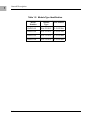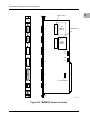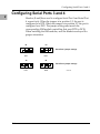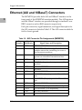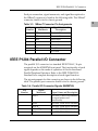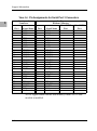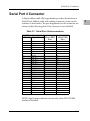
1
MVME760 Transition Module
User’s Manual
VME760A/UM1
Notice
While reasonable efforts have been made to assure the accuracy of this document,
Motorola, Inc. assumes no liability resulting from any omissions in this document,
or from the use of the information obtained therein. Motorola reserves the right to
revise this document and to make changes from time to time in the content hereof
without obligation of Motorola to notify any person of such revision or changes.
No part of this material may be reproduced or copied in any tangible medium, or
stored in a retrieval system, or transmitted in any form, or by any means, radio,
electronic, mechanical, photocopying, recording or facsimile, or otherwise,
without the prior written permission of Motorola, Inc.
It is possible that this publication may contain reference to, or information about
Motorola products (machines and programs), programming, or services that are
not announced in your country. Such references or information must not be
construed to mean that Motorola intends to announce such Motorola products,
programming, or services in your country.
Restricted Rights Legend
If the documentation contained herein is supplied, directly or indirectly, to the U.S.
Government, the following notice shall apply unless otherwise agreed to in
writing by Motorola, Inc.
Use, duplication, or disclosure by the Government is subject to restrictions as set
forth in subparagraph (c)(1)(ii) of the Rights in Technical Data and Computer
Software clause at DFARS 252.227-7013.
Motorola, Inc.
Computer Group
2900 South Diablo Way
Tempe, Arizona 85282
Preface
The MVME760 User’s Manual provides general information, hardware
preparation, installation instructions and support information for the MVME760
Transition Module.
The MVME760 module is used as the interface between host VMEmodules and
various peripheral devices. A ribbon cable is used to connect the MVME760
Transition Module to the host VMEmodule.
This manual is intended for anyone who wants to design OEM systems, supply
additional capability to an existing compatible system, or for use in a lab
environment for experimental purposes.
A basic knowledge of computers and digital logic is assumed.
To use this manual you should be familiar with the publications listed in the
following section: Related Documentation.
Related Documentation
The Motorola publications listed below are referenced in this document. If not
shipped with this product, manuals may be purchased by contacting your local
Motorola sales office.
Document Title
Motorola
Publication
Number
MVME1603/MVME1604 Single Board Computer Installation and Use V1600-1A/IH
MVME1603/MVME1604 Single Board Computer Programmer’s
V1600-1A/PG
Reference Guide
MVME1603/MVME1604 Support Information
V1600-1A/SC
PM603/PM604 Processor/Memory Mezzanine Module User’s Manual PM603A/UM
PPCBug Debugging Package User’s Manual (Parts 1 and 2)
PPCBUGA1/UM
PPCBUGA2/UM
PPC1Bug Diagnostics Manual
PPC1DIAA/UM
SIM705 Serial Interface Module Installation Guide
SIM705A/IH
Note
Although not shown in the above list, each Motorola Computer
Group manual publication number is suffixed with characters
which represent the revision level of the document, such as “/
D2” (the second revision of a manual); a supplement bears the
same number as the manual but has a suffix such as “/A1” (the
first supplement to the manual).
Motorola® and the Motorola symbol are registered trademarks of Motorola, Inc.
AIX™ is a trademarks of IBM.
PowerPC™ is a trademark of IBM, and is used by Motorola with permission.
All other products mentioned in this document are trademarks or registered
trademarks of their respective holders.
© Copyright Motorola 1995
All Rights Reserved
Printed in the United States of America
January 1995
Safety Summary
Safety Depends On You
The following general safety precautions must be observed during all phases of operation, service, and
repair of this equipment. Failure to comply with these precautions or with specific warnings elsewhere in
this manual violates safety standards of design, manufacture, and intended use of the equipment.
Motorola, Inc. assumes no liability for the customer's failure to comply with these requirements.
The safety precautions listed below represent warnings of certain dangers of which Motorola is aware. You,
as the user of the product, should follow these warnings and all other safety precautions necessary for the
safe operation of the equipment in your operating environment.
Ground the Instrument.
To minimize shock hazard, the equipment chassis and enclosure must be connected to an electrical ground.
The equipment is supplied with a three-conductor ac power cable. The power cable must either be plugged
into an approved three-contact electrical outlet or used with a three-contact to two-contact adapter, with
the grounding wire (green) firmly connected to an electrical ground (safety ground) at the power outlet.
The power jack and mating plug of the power cable meet International Electrotechnical Commission (IEC)
safety standards.
Do Not Operate in an Explosive Atmosphere.
Do not operate the equipment in the presence of flammable gases or fumes. Operation of any electrical
equipment in such an environment constitutes a definite safety hazard.
Keep Away From Live Circuits.
Operating personnel must not remove equipment covers. Only Factory Authorized Service Personnel or
other qualified maintenance personnel may remove equipment covers for internal subassembly or
component replacement or any internal adjustment. Do not replace components with power cable
connected. Under certain conditions, dangerous voltages may exist even with the power cable removed. To
avoid injuries, always disconnect power and discharge circuits before touching them.
Do Not Service or Adjust Alone.
Do not attempt internal service or adjustment unless another person capable of rendering first aid and
resuscitation is present.
Use Caution When Exposing or Handling the CRT.
Breakage of the Cathode-Ray Tube (CRT) causes a high-velocity scattering of glass fragments (implosion).
To prevent CRT implosion, avoid rough handling or jarring of the equipment. Handling of the CRT should
be done only by qualified maintenance personnel using approved safety mask and gloves.
Do Not Substitute Parts or Modify Equipment.
Because of the danger of introducing additional hazards, do not install substitute parts or perform any
unauthorized modification of the equipment. Contact your local Motorola representative for service and
repair to ensure that safety features are maintained.
Dangerous Procedure Warnings.
Warnings, such as the example below, precede potentially dangerous procedures throughout this manual.
Instructions contained in the warnings must be followed. You should also employ all other safety
precautions which you deem necessary for the operation of the equipment in your operating environment.
!
WARNING
Dangerous voltages, capable of causing death, are present in
this equipment. Use extreme caution when handling, testing,
and adjusting.
!
WARNING
This equipment generates, uses, and can radiate electromagnetic energy. It may cause or be susceptible to electromagnetic interference (EMI) if not installed and used in a
cabinet with adequate EMI protection.
Contents
CHAPTER 1 General Information
Introduction ..................................................................................................................... 1-1
Features of the MVME760 Module ........................................................................... 1-1
Specifications ................................................................................................................... 1-2
Cooling Requirements .................................................................................................. 1-2
FCC Compliance............................................................................................................. 1-3
General Description ....................................................................................................... 1-3
CHAPTER 2 Hardware Preparation and Installation
Introduction ..................................................................................................................... 2-1
Unpacking Instruction .................................................................................................. 2-1
MVME760 Module Preparation ................................................................................. 2-1
Configuring Serial Ports 3 and 4................................................................................ 2-4
Installation Instructions................................................................................................ 2-5
CHAPTER 3 Support Information
Introduction ..................................................................................................................... 3-1
COM1 and COM2 Serial Ports ................................................................................... 3-3
Serial Ports 3 and 4......................................................................................................... 3-5
P2 Connector.................................................................................................................. 3-10
Ethernet (AUI and 10BaseT) Connectors .............................................................. 3-14
IEEE P1284 Parallel I/O Connector ........................................................................ 3-15
COM1 and COM2 Connectors ................................................................................. 3-16
Serial Port 3 Connectors ............................................................................................. 3-17
Serial Port 4 Connector ............................................................................................... 3-19
Serial I/O Data Rate .................................................................................................... 3-20
Ethernet Data Rate ....................................................................................................... 3-20
Parts Lists and Locations ........................................................................................... 3-20
Schematic Drawings .................................................................................................... 3-24
vii
INDEX
Index ....................................................................................................................IN-1
viii
List of Figures
Figure 2-1.
Figure 2-2.
Figure 2-3.
Figure 3-1.
Figure 3-2.
Figure 3-3.
Figure 3-4.
Figure 3-5.
Figure 3-6.
Figure 3-7.
MVME760 Connector Locations.................................................... 2-2
MVME760 Header Locations......................................................... 2-3
MVME760 Cable Connections ....................................................... 2-6
MVME760 Transition Module Block Diagram ............................ 3-2
COM1 and COM2 Configurations ................................................ 3-4
Ports 3/4 in EIA-232 DCE Configuration .................................... 3-6
Ports 3/4 in EIA-232 DTE Configuration..................................... 3-7
Ports 3/4 in EIA-530 DCE Configuration .................................... 3-8
Ports 3/4 in EIA-530 DTE Configuration..................................... 3-9
MVME760 Parts Location Drawing ............................................ 3-23
ix
x
List of Tables
Table 1-1. MVME760 Specifications................................................................... 1-2
Table 1-2. Module Type Identification............................................................... 1-4
Table 3-1. Connector P2 Interconnect Signals (MVME760).......................... 3-10
Table 3-2. AUI Connector Pin Assignments (MVME760) ............................ 3-14
Table 3-3. 10BaseT Connector Pin Assignments ............................................ 3-15
Table 3-4. Parallel I/O Connector Signals (MVME760)................................ 3-15
Table 3-5. COM1 and COM2 Interconnect Signals (MVME760) ................. 3-16
Table 3-6. Pin Assignments for Serial Port 3 Connectors ............................. 3-18
Table 3-7. Serial Port 4 Interconnections ......................................................... 3-19
Table 3-8. MVME760 Module Parts List.......................................................... 3-20
xi
xii
1General Information
1
Introduction
This manual provides general information, hardware preparation,
installation instructions, and support information for the
MVME760 Transition Module.
The MVME760 module is used as the interface between host
VMEmodules and various peripheral devices. A 64-pin ribbon
cable (P/N 30-W2514B02, 17” length) connects the MVME760
Transition Module to the host VMEmodule.
Features of the MVME760 Module
The features of the MVME760 module include industry-standard
connectors that interface to:
❏
Two EIA-232 asynchronous serial ports
❏
Two synchronous serial ports
❏
One parallel port (IEEE Standard 1284-I compliant)
❏
Ethernet interface (both AUI and 10BaseT)
❏
Two 60-pin connectors are provided to support existing MCG
Serial Interface Modules. Currently, there are four types of
SIMs available: EIA-232 DCE, EIA-232 DTE, EIA-530 DCE,
and EIA-530 DTE. The selection of these modules determines
the functionality of the two synchronous serial ports.
1-1
1
Specifications
Specifications
The MVME760 module specifications are shown in Table 1-1.
Table 1-1. MVME760 Specifications
Characteristics
Power Requirements
I/O Port Connectors Serial
Parallel
Ethernet
Operating temperature
Storage temperature
Relative Humidity
Physical
characteristics
(excluding front
panel)
Specifications
+ 5Vdc, 1A maximum (500 mA
typical)
+12Vdc, 100mA (w/o LAN
transceiver)
-12Vdc, 100mA
Two EIA-232 async serial ports
Two synchronous serial ports
One IEEE Std 1284-I compliant
parallel port
One AUI and One 10BaseT
0 degrees to 55 degrees C at point of
entry of forced air (approximately 5
CFM)
-40 degrees to 85 degrees C
5% to 90% (non-condensing)
Height
9.187 inches(233.35 mm)
Depth
3.200 inches(80.00 mm)
Thickness 0.063 inches (1.60 mm)
Cooling Requirements
The MVME760 module has minimal active circuitry. In general,
convection cooling will suffice. However, care must be taken such
that other system components or other external sources of heat do
not cause the actual operating temperature to exceed the specified
operating temperature.
1-2
General Information
FCC Compliance
The MVME760 module was tested in an FCC-compliant chassis,
and meets the requirements for Class A equipment. FCC
compliance was achieved under the following conditions:
1. Shielded cables on all external I/O ports.
2. Cable shields connected to earth ground via metal shell
connectors bonded to a conductive module front panel.
3. Conductive chassis rails connected to earth ground. This
provides the path for connecting shields to earth ground.
4. Front panel screws properly tightened.
For minimum RF emissions, it is essential that the conditions above
be implemented; failure to do so could compromise the FCC
compliance of the equipment containing the modules.
General Description
The MVME760 Transition Module provides the interface between
standard Ethernet, Parallel Port, and the Serial Port connectors and
the Host board P2 connector. The Ethernet and Parallel Ports
contain passive circuitry only. The I/O controllers themselves
reside in the host board. The Serial Ports contain active circuitry, to
provide multiplexing and buffering functions (reference Figure 3-1,
MVME760 Transition Module Block Diagram). The multiplexing
function is transparent to the user. Two 60-pin headers are
provided to support existing MCG Serial Interface Modules.
Currently, there are four types of Serial Interface modules available
as shown in Table 1-2:
1-3
1
1
General Description
Table 1-2. Module Type Identification
Model
Number
1-4
Module
Type
Part Number
SIM705-001
EIA-232 DCE
01-W3876Bxx
SIM705-002
EIA-232 DTE
01-W3877Bxx
SIM705-003
EIA-530 DCE
01-W3878Bxx
SIM705-004
EIA-530 DTE
01-W3879Bxx
2Hardware Preparation and
Installation
2
Introduction
This chapter provides unpacking instructions, hardware
preparation, and installation instructions for the MVME760
module.
Unpacking Instruction
Note
If the carton is damaged upon receipt, request that the
carrier’s agent be present during unpacking and
inspection of the equipment.
Unpack the equipment from the shipping carton. Refer to the
packing list and verify that all items are present. Save the packing
material for storing and reshipping of the equipment.
MVME760 Module Preparation
No preparation is necessary if Serial ports 3 and 4 are not used.
However, to ensure full functionality of Serial Port 3 and Serial Port
4, the MVME760 Transition Module must be properly configured.
Configuration is accomplished through jumper settings and SIM
module population options. The MVME760 connectors and header
locations are illustrated in Figure 2-1 and Figure 2-2. Note that
Serial Port 3 is available at J7, as well as at J5 on the front panel.
Serial Port 4 is available only via the J2 header
2-1
MVME760 Module Preparation
2
BASE BOARD
TRANSITION MODULE
COM1
P1
COM2
SERIAL
PORT 3
64-PIN 50-MIL
CABLE
P2
P2
PARALLEL
PORT
AUI
10BASET
1544 9410
Figure 2-1. MVME760 Connector Locations
2-2
Hardware Preparation and Installation
2
SERIAL PORT 4
MVME
760-001
COM1
J1
COM2
J3
J2
SIM
MODULE
(PORT 4)
J7
SIM
MODULE
(PORT 3)
SERIAL PORT 3
SERIAL 3
J8
J5
3
DCE
DTE
1
3
DCE
PARALLEL
J10
ETHERNET
J11
DTE
1
J9
F1
P2
1.1A. POLYSWITCH
10BASET
J12
1545 9410
Figure 2-2. MVME760 Header Locations
2-3
Configuring Serial Ports 3 and 4
Configuring Serial Ports 3 and 4
2
Headers J9 and J8 are used to configure Serial Port 3 and Serial Port
4, respectively. When the jumper is in position 1-2, the port is
configured as a DTE. When the jumper is in position 2-3, the port is
configured as a DCE. The jumper setting must match the
corresponding SIM module controlling that port (DTE or DCE).
When installing the SIM modules, note the headers are keyed for
proper orientation.
J9
J9
Serial Port 3 jumper settings
1
2
3
1
2
DTE
DCE
J8
J8
3
Serial Port 4 jumper settings
1
2-4
2
DTE
3
1
2
DCE
3
15446 9410
Hardware Preparation and Installation
Installation Instructions
2
The basic procedure for installation of the MVME760 module is as
follows:
1. Turn all equipment power OFF and disconnect the power
cable from the AC power source.
!
Connecting modules while the power is applied may
result in damage to components on the module.
Caution
!
Warning
Dangerous voltages, capable of causing death, are
present in this equipment. Use extreme caution when
handling, testing, and adjusting.
2. Remove the chassis cover as instructed in the equipment
user’s manual.
3. Remove the filler panel(s) from the appropriate card slot(s) at
the rear of the chassis (if the chassis has a rear card cage).
Other modules in the unit may have to be moved to allow
space for the cables connected to the MVME760 module.
4. Install SIM modules for Serial Ports 3 and 4 (see Figure 2-2 for
location of SIMs).
5. Install MVME760 module in rear card cage.
6. Attach the flat ribbon cable supplied with the MVME760
module from P2 on the host board to P2 on the Transition
Module. Be sure to orient cable pin 1 with connector pin 1 (See
Figure 2-3).
7. After making sure you will not pinch cables with the cover,
reinstall the cover you previously removed.
8. Connect the power cable to the AC power source and turn on
the unit.
2-5
Installation Instructions
2
MVME760
J1
HOST
J3
J5
P1
J10
1
J11
P2
1
J12
P2
P2
ENCLOSURE BOUNDARY
1548 9412
Figure 2-3. MVME760 Cable Connections
2-6
3Support Information
3
Introduction
This chapter provides the interconnection signals, parts lists, parts
location illustrations, and schematic diagrams for the MVME760
Transition Module.
The block diagram for the MVME760 Transition Module is shown
in Figure 3-1.
3-1
10BaseT
AUI
PARALLEL
COM1
COM2
SERIAL 3
RJ45
DB15
HD36
DB9
DB9
HD26
26-PIN 3M
SERIAL 3
SERIAL 4
26-PIN 3M
BUFFERS
EIA-232
BUFFERS
EIA-232
P2MX FUNCTION
CONNECTOR TO SERIAL MODULE
3
CONNECTOR TO SERIAL MODULE
Support Information
64-PIN DIN CONNECTOR
1549 9410
Figure 3-1. MVME760 Transition Module Block Diagram
3-2
COM1 and COM2 Serial Ports
COM1 and COM2 Serial Ports
COM1 and COM2 are the two asynchronous serial ports. These two
ports are configured as shown in Figure 3-2.
3-3
3
Support Information
3
TXD1
C19
3
RTS1_
A20
7
DTR1_
C20
4
RXD1
A17
2
CTS1_
C17
8
DSR1_
A18
6
DCD1_
C18
1
RI1_
A19
9
COM1
5
P2
TXD2
C24
3
RTS2_
A24
7
DTR2_
C25
4
RXD2
A21
2
CTS2_
C22
8
DSR2_
A22
6
DCD2_
C23
1
RI2_
A23
9
COM2
5
BASE
BOARD
MVME760
1550 9410
Figure 3-2. COM1 and COM2 Configurations
3-4
Serial Ports 3 and 4
Serial Ports 3 and 4
Serial Ports 3 and 4 can be individually configured as EIA-232-D
DCE, EIA-232-D DTE, EIA-530 DCE, or EIA-530 DTE by installing
the appropriate Serial Interface Module. Figure 3-3 and Figure 3-4
show the configuration diagrams for Serial Ports 3 and 4 with the
EIA-232 DCE and EIA-232 DTE Serial Interface Modules. Figure 35 and 3-6 show the configuration diagrams for Serial Ports 3 and 4
with the EIA-530 DCE and EIA-530 DTE Serial Interface Modules.
3-5
3
Support Information
Z85230 SCC
P2/P2MX
3M
DB25
(Port 3 only)
TXD
5
3
RXD
RTS_
9
5
CTS
RXD
3
2
TXD
CTS_
7
4
RTS
DCD_
14
20
DTR
3
4
15
TXCI
2
1
8
17
RXCI
22
24
TXCO
DTR_
15
8
DCD
LLB_
24
25
TM
RLB_
18
22
RI
DSR_
11
6
DSR
RI_
16
21
RLB
TM_
10
18
LLB
13
7
GND
3
TRXC
J9, J8
RTXC
Z8536 CIO
EIA232-DCE SIM
1554 9411
Figure 3-3. Ports 3/4 in EIA-232 DCE Configuration
3-6
Serial Ports 3 and 4
Z85230 SCC
P2/P2MX
3M
DB25
(Port 3 only)
TXD
3
2
TXD
RTS_
7
4
RTS
RXD
5
3
RXD
CTS_
9
5
CTS
DCD_
15
8
DCD
3
22
24
TXCO
2
1
4
15
TXCI
8
17
RXCI
DTR_
14
20
DTR
LLB_
10
18
LLB
RLB_
16
21
RLB
DSR_
11
6
DSR
RI_
18
22
RI
TM_
24
25
TM
13
7
GND
TRXC
J9, J8
RTXC
Z8536 CIO
EIA232-DTE SIM
1555 9411
Figure 3-4. Ports 3/4 in EIA-232 DTE Configuration
3-7
3
Support Information
Z85230
SIM08
EIA-530 DCE
P2/P2MX
FRONT PANEL
DB25
(Port 3 only)
3M
PORTS 3, 4
3
NC
TXD
2
D
3
6
5
R
RXD
RTS_
12
D
7
25
CTS _
R
PIN 1
1
9
20
14
TXD_B
TXD_A
RXD_B
RXD_A
PIN 14
PIN 2
PIN 16
PIN 3
RTS_B
RTS_A
CTS_B
CTS_A
PIN 19
PIN 4
PIN 13
PIN 5
DTR_B
DTR_A
PIN 23
PIN 20
R
DCD_
DSR_B
D
18
11
DSR_A
PIN 22
PIN 6
TXC_B
J9, J8
+5V
1
TRXC
D
23
4
TXC_A
PIN 12
PIN 15
RXC_B
2
D
17
8
3
RXC_A
PIN 9
PIN 17
TXCO_B
R
RTXC
21
22
+5V
24
D
TXCO_A
TM_A
PIN 11
PIN 24
PIN 25
LL_A
10
NC
16
PIN 21
13
PIN 7
RL_A
Z8536 CIO
DTR_
PIN 18
NC
D
10
DCB_B
DCD_A
15
PIN 10
PIN 8
1557 9412
Figure 3-5. Ports 3/4 in EIA-530 DCE Configuration
3-8
Serial Ports 3 and 4
Z85230
SIM08
EIA-530 DTE
P2/P2MX
FRONT PANEL
DB25
(Port 3 only)
3M
PORTS 3, 4
NC
3
PIN 1
1
TXD_B
TXD
2
D
TXD_A
PIN 2
3
RXD
6
5
R
RTS_
12
D
7
25
CTS _
R
9
RXD_B
RXD_A
PIN 16
PIN 3
RTS_B
RTS_A
PIN 19
PIN 4
CTS_B
PIN 13
CTS_A
PIN 5
DCD_B
19
15
R
DCD_
PIN 14
DCD_A
PIN 10
PIN 8
DSR_B
18
11
R
NC
J9, J8
1
DSR_A
PIN 22
PIN 6
TXC_B
23
4
R
+5V
TXC_A
PIN 12
PIN 15
RXC_B
2
17
8
R
TRXC
RXC_A
PIN 9
PIN 17
TXCO_B
21
22
D
3
RTXC
NC
24
TXCO_A
TM_A
PIN 11
PIN 24
PIN 25
LL_A
+5V
D
PIN 18
10
RL_A
D
+5V
Z8536 CIO
DTR_
D
16
PIN 21
13
PIN 7
20
DTR_B
DTR_A
14
PIN 23
PIN 20
1558 9412
Figure 3-6. Ports 3/4 in EIA-530 DTE Configuration
3-9
Support Information
P2 Connector
P2 is a 64-pin DIN connector providing power and signaling. The
64-pin ribbon cable P/N is 30-W2514B02. Table 3-1 shows the
interconnect signals. Note Row B is not populated. Power
distribution and signaling are accomplished using rows A and C
only.
3
Table 3-1. Connector P2 Interconnect Signals (MVME760)
Pin
Number
Signal
Mnemonic
Signal Name and Description
P2
C1
C+
COLLISION + (Input) (Ethernet) - a signal to indicate that
multiple stations are contending for access to the
transmission medium.
A1
CCOLLISION - (Input) (Ethernet) - part of a differential pair.
C2
T+
TRANSMIT + (Output) (Ethernet) - this line is intended to
operate into terminated transmission lines.
A2
TTRANSMIT - (Output) (Ethernet) - part of a differential pair.
C3
R+
RECEIVE + (Input) (Ethernet) - a data input sourced by the
MAU.
A3
RRECEIVE - (Input) (Ethernet) - part of a differential pair.
C4
RDRECEIVE DATA A4
RD+
RECEIVE DATA+
C5
TDTRANSMIT DATAA5
TD+
TRANSMIT DATA+
C6
+12V
+12Vdc Power
A6
PRD0
Refer to the IEEE P1284 D2.00 Standard
C7
PRD1
Refer to the IEEE P1284 D2.00 Standard
A7
PRD2
Refer to the IEEE P1284 D2.00 Standard
C8
PRD3
Refer to the IEEE P1284 D2.00 Standard
A8
PRD4
Refer to the IEEE P1284 D2.00 Standard
C9
PRD5
Refer to the IEEE P1284 D2.00 Standard
A9
PRD6
Refer to the IEEE P1284 D2.00 Standard
C10
PRD7
Refer to the IEEE P1284 D2.00 Standard
3-10
P2 Connector
Table 3-1. Connector P2 Interconnect Signals (MVME760) (Continued)
Pin
Number
P2
A10
C11
A11
C12
A12
C13
A13
C14
A14
C15
A15
C16
A16
C17
GND
PRSTB_
PRACK_
GND
PRBSY
PRPE
PRSEL
INPRIME_
PRFAULT_
SELIN_
AUTOFD_
+5V
GND
CTS1
SIGNAL GROUND
Refer to the IEEE P1284 D2.00 Standard
Refer to the IEEE P1284 D2.00 Standard
SIGNAL GROUND
Refer to the IEEE P1284 D2.00 Standard
Refer to the IEEE P1284 D2.00 Standard
Refer to the IEEE P1284 D2.00 Standard
Refer to the IEEE P1284 D2.00 Standard
Refer to the IEEE P1284 D2.00 Standard
Refer to the IEEE P1284 D2.00 Standard
Refer to the IEEE P1284 D2.00 Standard
+5Vdc Power
SIGNAL GROUND
CLEAR TO SEND (serial port 1) - CTS is a function supplied
to the terminal by the modem, and indicates that it is
permissible to begin transmission of a message. When using
a modem, CTS follows the off-to-on transition of RTS after a
time delay.
A17
RXD1
C18
DCD1
A18
DSR1
C19
TXD1
A19
RI1
RECEIVE DATA (serial port 1) - data that is demodulated
from the receive line is presented to the terminal by the
modem.
DATA CARRIER DETECT (serial port 1) - sent by the
modem to the terminal to indicate that a valid carrier is
being received.
DATA SET READY (serial port 1) - a function supplied by
the modem to the terminal to indicate that the modem is
ready to transmit data.
TRANSMIT DATA (serial port 1) - data to be transmitted is
furnished on this line to the modem from the terminal.
RING INDICATOR (serial port 1) - Sent by the modem to
the terminal indicating the ringing signal is present.
Signal
Mnemonic
Signal Name and Description
3
3-11
Support Information
Table 3-1. Connector P2 Interconnect Signals (MVME760) (Continued)
3
Pin
Number
Signal
Mnemonic
Signal Name and Description
P2
C20
DTR1
DATA TERMINAL READY (serial port 1) - a signal from the
terminal to the modem indicating that the terminal is ready
to send or receive data.
A20
RTS1
REQUEST TO SEND (serial port 1) - RTS is supplied by the
terminal to the modem when it is required to transmit a
message. With RTS off, the modem carrier remains off.
When RTS is turned on, the modem immediately turns on
the carrier.
A21
RXD2
RECEIVE DATA (serial port 2) - data that is demodulated
from the receive line is presented to the terminal by the
modem.
C21
GND
SIGNAL GROUND
C22
CTS2
CLEAR TO SEND (serial port 2) - CTS is a function supplied
to the terminal by the modem, and indicates that it is
permissible to begin transmission of a message. When using
a modem, CTS follows the off-to-on transition of RTS after a
time delay.
A22
DSR2
DATA SET READY (serial port 2) - a function supplied by
the modem to the terminal to indicate that the modem is
ready to transmit data.
C23
DCD2
DATA CARRIER DETECT (serial port 2) - sent by the
modem to the terminal to indicate that a valid carrier is
being received.
A23
RI2
RING INDICATOR (serial port 2) - Sent by the modem to
the terminal indicating the ringing signal is present.
C24
TXD2
TRANSMIT DATA (serial port 2) - data to be transmitted is
furnished on this line to the modem from the terminal.
A24
RTS2
REQUEST TO SEND (serial port 2) - RTS is supplied by the
terminal to the modem when it is required to transmit a
message. With RTS off, the modem carrier remains off.
When RTS is turned on, the modem immediately turns on
the carrier.
3-12
P2 Connector
Table 3-1. Connector P2 Interconnect Signals (MVME760) (Continued)
Pin
Number
Signal
Mnemonic
Signal Name and Description
P2
C25
DTR2
DATA TERMINAL READY (serial port 2) - a signal from the
terminal to the modem indicating that the terminal is ready
to send or receive data.
A25
GND
SIGNAL GROUND
C26
RXD3
RECEIVE DATA (serial port 3) - data that is demodulated
from the receive line is presented to the terminal by the
modem.
A26
RTXC3
RECEIVE CLOCK (serial port 3) - this line can be
configured to clock input data from a terminal to a modem.
C27
TXD3
TRANSMIT DATA (serial port 3) - data to be transmitted is
furnished on this line to the modem from the terminal.
A27
TRXC3
TRANSMIT CLOCK (serial port 3) - this line can be
configured to clock output data to the modem from the
terminal.
C28
RXD4
RECEIVE DATA (serial port 4) - data that is demodulated
from the receive line is presented to the terminal by the
modem.
A28
RTXC4
RECEIVE CLOCK (serial port 4) - this line can be
configured to clock input data from a terminal to a modem.
C29
TXD4
TRANSMIT DATA (serial port 4) - data to be transmitted is
furnished on this line to the modem from the terminal.
A29
TRXC4
TRANSMIT CLOCK (serial port 4) - this line can be
configured to clock output data to the modem from the
terminal.
C30
-12V
-12Vdc Power
A30
MXDI
C31
MXDO
A31
C32
A32
MXSYNC_
GND
MXCLK
Serial MULTIPLEXER DATA IN - signal driven to the main
board.
Serial MULTIPLEXER DATA OUT - received from main
board.
MULTIPLEXER SYNC - Serial Multiplexer sync signal.
SIGNAL GROUND
MULTIPLEXER CLOCK - Serial Multiplexer clock signal.
3-13
3
Support Information
Ethernet (AUI and 10BaseT) Connectors
The MVME760 provides both AUI and 10BaseT interface via the
front panel of the MVME760 transition module. The AUI interface
and the 10BaseT interface are provided through a standard 2-row
DB15 connector and an RJ45 connector respectively.
3
Each pin connection, signal mnemonic, and signal description for
the AUI connector is listed in Table 3-2. The AUI connector shield is
tied to chassis ground.
Table 3-2. AUI Connector Pin Assignments (MVME760)
Pin
Number
1
2
3
4
5
6
7
8
9
10
11
12
13
14
15
3-14
Signal
Mnemonic
Signal Name and Description
GND
SIGNAL GROUND.
C+
COLLISION + (Input) - a signal to indicate that
multiple stations are contending for access to
the transmission medium.
T+
TRANSMIT + (Output) - this line is intended to
operate into terminated transmission lines.
GND
SIGNAL GROUND.
R+
RECEIVE + (Input) - a data input sourced by
the MAU.
GND
SIGNAL GROUND.
Not used.
GND
SIGNAL GROUND.
CCOLLISION - (Input) - part of a differential
pair.
TTRANSMIT - (Output) - part of a differential
pair.
GND
SIGNAL GROUND.
RRECEIVE - (Input) - part of a differential pair.
+12VF
+12 Vdc Power -(1.1A Polyswitch)
GND
SIGNAL GROUND.
Not used.
IEEE P1284 Parallel I/O Connector
Each pin connection, signal mnemonic, and signal description for
the 10BaseT connector is listed in the following table. The 10BaseT
connector shield is tied to chassis ground.
3
Table 3-3. 10BaseT Connector Pin Assignments
Pin
Number
1
2
3
4
5
6
7,8
Signal
Mnemonic
TD+
TDRD+
RD-
Signal Name and
Description
Transmit Data+
Transmit DataRead Data+
Not used.
Not used.
Read DataNot used.
IEEE P1284 Parallel I/O Connector
The parallel I/O connector is a standard IEEE P1284-C, 36-pin
receptacle on the MVME760 front panel. The functionality of each
signal depends on the mode of operation of this bi-directional
Parallel Peripheral Interface. Refer to the IEEE P1284 D2.00
Standard for a complete description of each signal function.
The pin assignments for this connector are shown in the following
table. The parallel port connector shield is tied to chassis ground.
Table 3-4. Parallel I/O Connector Signals (MVME760)
Pin
Number
1
Signal
Mnemonic
PRBSY
2
3
4
5
PRSEL
PRACK_
PRFAULT_
PRPE
Signal Name and Description
See IEEE P1284 D2.00 Standard
for signal names and
functionality.
See IEEE P1284 D2.00 Standard
See IEEE P1284 D2.00 Standard
See IEEE P1284 D2.00 Standard
See IEEE P1284 D2.00 Standard
3-15
Support Information
Table 3-4. Parallel I/O Connector Signals (MVME760) (Continued)
Pin
Number
3
6
7
8
9
10
11
12
13
14
15
16
17
18
19-25
Signal
Mnemonic
PRD0
PRD1
PRD2
PRD3
PRD4
PRD5
PRD6
PRD7
INPRIME_
PRSTB_
SELIN_
AUTOFD_
+5V
GND
Signal Name and Description
See IEEE P1284 D2.00 Standard
See IEEE P1284 D2.00 Standard
See IEEE P1284 D2.00 Standard
See IEEE P1284 D2.00 Standard
See IEEE P1284 D2.00 Standard
See IEEE P1284 D2.00 Standard
See IEEE P1284 D2.00 Standard
See IEEE P1284 D2.00 Standard
See IEEE P1284 D2.00 Standard
See IEEE P1284 D2.00 Standard
See IEEE P1284 D2.00 Standard
See IEEE P1284 D2.00 Standard
+5Vdc Power
SIGNAL GROUND
COM1 and COM2 Connectors
Two standard DB9 connectors located on the front panel of the
MVME760 transition module provide the interface to the COM1
and COM2 serial ports. The pin assignments for these connectors
are shown in Table 3-5. The COM1 and COM2 connector shields are
tied to chassis ground.
Table 3-5. COM1 and COM2 Interconnect Signals (MVME760)
Pin
Number
1
3-16
Signal
Mnemonic
Signal Name and Description
DCD
DATA CARRIER DETECT - Sent by the modem to
the terminal to indicate that a valid carrier is being
received. Not used by port 1 (J1).
Serial Port 3 Connectors
Table 3-5. COM1 and COM2 Interconnect Signals (MVME760) (Continued)
Pin
Number
2
3
4
5
6
7
8
9
Signal
Mnemonic
Signal Name and Description
RXD
RECEIVE DATA - data that is demodulated from
the receive line is presented to the terminal by the
modem.
TXD
TRANSMIT DATA - data to be transmitted is
furnished on this line to the modem from the
terminal.
DTR
DATA TERMINAL READY - A signal from the
terminal to the modem indicating that the terminal
is ready to send or receive data.
GND
SIGNAL GROUND
DSR
DATA SET READY - DSR is a function supplied by
the modem to the terminal to indicate that the
modem is ready to transmit data. This signal can be
held high or low through header J8, J9, J13, J14.
RTS
REQUEST TO SEND - RTS is supplied by the
terminal to the modem when it is required to
transmit a message. With RTS off, the modem
carrier remains off. When RTS is turned on, the
modem immediately turns on the carrier.
CTS
CLEAR TO SEND - CTS is a function supplied to
the terminal by the modem, and indicates that it is
permissible to begin transmission of a message.
When using a modem, CTS follows the off-to-on
transition of RTS after a time delay.
RI
RING INDICATOR - Sent by the modem to the
terminal indicating the ringing signal is present.
3
Serial Port 3 Connectors
Two connectors are provided for Serial Port 3: A 26-pin mini delta
ribbon connector located on the front panel of the MVME760
transition module and a 26-pin ribbon-cable (3M-type) header
located on the board itself. The pin assignments for these two
connectors are shown in Table 3-6. The mini delta ribbon connector
shield is tied to chassis ground.
3-17
Support Information
Table 3-6. Pin Assignments for Serial Port 3 Connectors
Front-panel
Connector
3
Pin #
1
2
3
4
5
6
7
8
9
10
11
12
13
14
15
16
17
18
19
20
21
22
23
24
25
26
Signal Name
No Connect
TXD3
RXD3
RTS3
CTS3
DSR3
GND
DCD3
SP3_P9
SP3_P10
SP3_P11
SP3_P12
SP3_P13
SP3_P14
TXCI3
SP3_P16
RXCI3
LLB3
SP3_P19
DTR3
RLB3
RI3
SP3_P23
TXCO3
TM3
No Connect
Pin #
1
3
5
7
9
11
13
15
17
19
21
23
25
2
4
6
8
10
12
14
16
18
20
22
24
26
3m-Type
Ribbon Connector
Mated DB25
Signal Name
Pin #
No Connect
1
TXD3
2
RXD3
3
RTS3
4
CTS3
5
DSR3
6
GND
7
DCD3
8
SP3_P9
9
SP3_P10
10
SP3_P11
11
SP3_P12
12
SP3_P13
13
SP3_P14
14
TXCI3
15
SP3_P16
16
RXCI3
17
LLB3
18
SP3_P19
19
DTR3
20
RLB3
21
RI3
22
SP3_P23
23
TXCO3
24
TM3
25
No Connect
Mated DB26
Pin #
1
2
3
4
5
6
7
8
9
10
11
12
13
14
15
16
17
18
19
20
21
22
23
24
25
26
NOTE: signal names indicate functionality when EIA-232 SIM
module is installed.
3-18
Serial Port 4 Connector
Serial Port 4 Connector
A 26-pin ribbon-cable (3M-type) header provides the interface to
Serial Port 4. Ribbon cable with mating connector can be used to
interface to this header. The pin assignments for this connector are
shown in the following table. This connector is not shielded.
Table 3-7. Serial Port 4 Interconnections
Ribbon Connector
Pin #
Signal Name
1
3
5
7
9
11
13
15
17
19
21
23
25
2
4
6
8
10
12
14
16
18
20
22
24
26
No Connect
TXD4
RXD4
RTS4
CTS4
DSR4
GND
DCD4
SP4_P9
SP4_P10
SP4_P11
SP4_P12
SP4_P13
SP4_P14
TXCI4
SP4_P16
RXCI4
LLB4
SP4_P19
DTR4
RLB4
RI4
SP4_P24
TXCO4
TM4
No Connect
Mated DB25
Pin #
1
2
3
4
5
6
7
8
9
10
11
12
13
14
15
16
17
18
19
20
21
22
23
24
25
Mated DB26
Pin #
1
2
3
4
5
6
7
8
9
10
11
12
13
14
15
16
17
18
19
20
21
22
23
24
25
26
NOTE: Signal names indicate functionality when EIA-232 SIM
module is installed.
3-19
3
Support Information
Serial I/O Data Rate
The serial data rate supported depends on the host board
implementation. Refer to related documentation.
3
Ethernet Data Rate
The Ethernet data rate supported depends on the host board
implementation. Refer to related documentation.
Parts Lists and Locations
The following parts lists and parts location drawings reflect the latest issue of
hardware at the time of printing.
Parts lists are illustrated in Table 3-8. Parts locations are illustrated in Figure 3-7.
Model
MVME760
Parts List
Table 3-8
Parts Location Drawing
Figure 3-7
Table 3-8. MVME760 Module Parts List
Reference
Designation
Motorola
Part Number
84-W8000F01A
CR1,CR2
48NW963A04
C1-12,16,17,23, 21NW9711A02
30,35-40, 42,
43,45,46,49,50,
C13,18
21NW9711A20
C14,19,32-34
21NW9711A21
C15,20-22,2421NW9711A29
26,29
C27,28
C31, 48
3-20
21NW9711A12
23NW9712A04
Description
Printed wiring board (MVME760)
Rectifier, Schottky
Capacitor, fixed,ceramic,100KpF
Capacitor, fixed, ceramic, 220pF
Capacitor, fixed, ceramic, 47pF
Capacitor, fixed, ceramic, 470pF
Capacitor, fixed, ceramic, 680pF
Capacitor, fixed, 10 µF @25 Vdc
Parts Lists and Locations
Table 3-8. MVME760 Module Parts List (Continued)
Reference
Designation
C41
C44,47,51
F1
J1, 3
J2, 7
J4, 6
J5
J8, J9
J10
J11
J12
P2
R1, 2
Motorola
Part Number
23NW9712A06
21NW9711A11
06NW9650A01
28NW9802H73
28NW9802G11
28-W6249B01
28NW9802K30
29NW9805C07
28NW9802K76
28NW9802J64
28NW9802K05
28NW9802E05
51NW9635A28
R3
R4, 11, 12, 14,
15
R5-8
R9, 10, 13
06SW-965A14
06SW965A24
R16
R17
R18, 19
R20, 21
U1-4
U5,6
U7, 8, 10
U9
U11
U12
U13, 16
51NW9635A35
51NW9635A06
06SW-965B62
06SW-965A02
51NW9615Z19
51-W5888B88
51NW9637D11
51NW9615P91
51NW9615P82
51NW9615Y31
51NW9637E49
51NW9635A13
51NW9635A14
Description
Capacitor, fixed, 33 µF @15 Vdc
Capacitor, fixed, ceramic, 22pF
Polyswitch, 1.1A
Connector, 9-pin plug
Connector, 26-pin
Connector, receptacle, SMT2X30
Connector, 26-pin miniature
Pin, square, auto-insert
Connector, 36-pin receptacle
Connector, 15-pin socket
Modular jack, 8-pin, shielded
Connector, 64-pin plug “PWB”
Resistor network, 16-pin, 8-100 ohm,
2%
Resistor, SMD, 1K ohm, 5%, 1/8 W
Resistor, SMD, 22 ohm, 5%, 1/8 W
3
Resistor network, 16-pin, 8-22 ohm, 2%,
Resistor network, 16-pin, 15-10K ohm,
2%
Resistor network, 16-pin, 15-4.7K ohm
Resistor network, 16-pin, 8-33 ohm, 2%
Resistor, SMD, 33 ohm, 1/8W, 5%
Resistor, SMD, 100 ohm, 1/8 W, 5%
I.C. MC145406DW,16-pin
I.C., PAL
I.C., SN74BCT244DB, 20-pin
I.C., N74F04D, 14-pin
I.C., N74F74D, 14-pin
I.C., N74F163AD, 16-pin
I.C., MC74F251D, 16-pin
3-21
Support Information
Table 3-8. MVME760 Module Parts List (Continued)
Reference
Designation
U14, 15
3
3-22
Motorola
Part Number
51NW9637C20
64-W4478C01A
30-W2514B02
Description
I.C., MC74F257AD, 16-pin
Front Panel (MVME760-001)
17” length, 64-pin ribbon cable
Parts Lists and Locations
60
59
C3
U2
C6
C5
2
1
1
2
60
59
C7
C8
J6
U4
C10
C9
J7
25
13
U3
25
26
VR16
5
VR15
6
VR14 VR13
R2
J3
1
2
3
J8
C17
C16
C29
1
2
15
R3
2
1
C12
C11
J5
1
R5
J9
3
U6
1
U5
1
C20
C22
C25
C24
C21
C26
1
C15
R17
R6
36
17
U7
C23
A1
C1
+
C19
R18
C13
R19
C18
R4
J10
C31
U8
C14
C30
1
2
20
PARALLEL
CR1
U10
R22
R23
C36
C32 C35
R20
R21
C28
C34
C33
R8
C27
15
8
F1
P2
C37
C41
C40
C39
C44
1
C42
2
9
C38
J11
ETHERNET
+
C47
C48
R15
CR2
R11
R14
C46
J12
8
7
R12
C43
C45
2
1
10BASET
A32
C32
C51
U16
C50
C49
U15
U13
J4
C4
J2
VR11
VR12
9
1
VR9
5
VR8 VR10
VR7
6
SERIAL 3
R13
U14
C2
U1
25
26
R1
J1
COM2
R10
U9
R9
U12
U11
C1
VR3 VR6
VR2 VR5
VR1 VR4
9
1
COM1
R7
R16
3
MVME
760-001
1551 9410
Figure 3-7. MVME760 Parts Location Drawing
3-23
Support Information
Schematic Drawings
Schematic drawings for the MVME760 Transition Module are
shown on the following pages.
3
3-24
Index
When using this index, keep in mind that a page number indicates only where
referenced material begins. It may extend to the page or pages following the page
referenced.
Numerics
I
10BaseT Connector Pin Assignments
I/O Ports 1-2
IEEE P1284 Parallel I/O Connector 3-15
Installation Instructions 2-5
3-15
A
AUI Connector Pin Assignments 3-14
J
J9 and J8 2-4
B
block diagram 3-1
M
Module Preparation 2-1
C
Cable Connections 2-6
COM1 and COM2 Connectors 3-16
COM1 and COM2 Serial Ports 3-3
Configuring Serial Ports 3 and 4 2-4
Connector P2 Interconnect Signals 3-10
Cooling Requirements 1-2
E
EIA-232D
interconnect signals 3-16
Ethernet (AUI & 10BaseT)Connectors
3-14
Ethernet Data Rate 3-20
F
FCC Compliance 1-3
G
General Description 1-3
O
Operating temperature 1-2
P
P2 Connector 3-10
Parallel I/O Connector Signals 3-15
parts lists 3-20
Parts Lists and Locations 3-20
Ports 3-8
Ports 3/4 in EIA232-DCE Configuration 3-6
Ports 3/4 in EIA232-DTE Configuration 3-7
Ports 3/4 in EIA-530 DCE Configuration 3-8
Ports 3/4 in EIA-530 DTE Configuration 3-9
Power Requirements 1-2
R
RF emissions 1-3
IN-1
Index
S
Schematic Drawings 3-22, 3-24
Serial I/O Data Rate 3-20
Serial Interface Modules 1-3
Serial Port 4 Connector 3-19
Serial Ports 3 and 4 3-5
Specifications 1-2
Storage temperature 1-2
U
Unpacking Instruction 2-1
I
N
D
E
X
IN-2