1
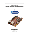
SR-uSOM-MX6 User Manual Freescale i.MX6™ based MicroSOM |Page1 Documentation Revision History Date 18-June-2014 19-June-2014 09-November-2014 Owner Rabeeh Khoury Kossay Omary Ohad Barany Revision 1.0 Notes Initial release 1.1 1.2 Review and slight fixes Change picture, add products description and add ordering information Disclaimer No warranty of accuracy is given concerning the contents of the information contained in this document. To the extent permitted by law no liability (including liability to any person by reason of negligence) will be accepted by SolidRun Ltd. or its employees for any direct or indirect loss or damage caused by omissions from or inaccuracies in this document .SolidRun Ltd. reserves the right to change details in this publication without notice. Product and company names herein may be the trademarks of their respective owners. |Page2 Contents Introduction .................................................................................................................4 Overview .....................................................................................................................4 The SR-uSOM-MX6 Highlighted Features .....................................................................4 The SR-uSOM-MX6 Supporting Products ......................................................................4 The SR-uSOM-MX6 Features Summary ........................................................................4 Block Diagram of the SR-uSOM-MX6 ...........................................................................5 Core System Components ..............................................................................................6 i.MX6 SoC Family.......................................................................................................6 10/100/1000 Mbps Ethernet PHY................................................................................8 Wireless LAN 802.11 b/g/n and Bluetooth 4.0 SiP .........................................................9 SR-uSOM-MX6 Interfaces ............................................................................................ 10 SR-uSOM-MX6 External Interfaces ............................................................................ 10 SR-uSOM-MX6 On Board Functions ........................................................................... 11 10/100/1000 Mbps PHY ....................................................................................... 11 802.11 b/g/n and Bluetooth SiP ............................................................................. 11 SR-uSOM-MX6 External Interfaces Detailed Description .................................................. 12 Main Board to Board Header .................................................................................... 13 Second Board to Board Header ................................................................................. 15 Third Board to Board Header .................................................................................... 17 SR-uSOM-MX6 Integration Manual ............................................................................... 19 SR-uSOM-MX6 Power Up Sequence .......................................................................... 19 SR-uSOM-MX6 Debugging Capability ......................................................................... 20 Differences between SR-uSOM-MX6 Versions ............................................................ 20 SR-uSOM-MX6 Typical Power Consumption ............................................................... 21 SR-uSOM-MX6 Maximum Rating ............................................................................... 22 SR-uSOM-MX6 Mechanical Description...................................................................... 23 Ordering Information .................................................................................................. 24 Notes ..................................................................................................................... 24 Federal Communications Commission (FCC) Statement ................................................ 25 Canadian Compliance .............................................................................................. 25 operation of the device. ........................................................................................... 25 |Page3 Introduction This User Manual relates to SolidRun SR-uSOM-MX6 series which includes the single core ARM A9 (1 GHz) of the i.MX6 SoC:uSOM-i1 (C1000S-D512-FE), the dual lite core ARM A9 (1GHz) of the i.MX6 SoC: uSOM-i2 (C1000DL-D1024-FE), the dual core ARM A9 (1GHz) of the i.MX6 SoC: uSOM-i2eX (C1000DM-D1024-GE-W) and the quad core ARM A9 (1GHz) of the i.MX6 SoC: uSOM-i4 (C1000QM-D2048-GE-W). Overview The SolidRun SR-uSOM-MX6 is a high performance micro system on module that is based on the highly integrated Freescale i.MX6 family of products. The SR-uSOM-MX6 Highlighted Features Ultra small MicroSOM (47x30mm) with 3 board to board connectors. Mating height is carrier board dependent. Freescale i.MX6 SoC (supports solo, dual lite, dual and quad versions) o Up to quad Cortex A9 and up to 1.2GHz o Integrated multi format decoders and encoders, de-interlacing and color conversion functions o Integrated OpenVG, OpenGL ES 2.0 and OpenCL 1.1 EP GPU DDR3 memories in x32 or x64 configurations (either 2 x16 or 4 x16 on a single chip select) Power management devices Gigabit Ethernet phy based on Qualcomm Atheros 8035 (footprint compatible with 8030 fast Ethernet phy) Broadcom BCM4330 based WiFi 11n and Bluetooth 4.0 (2.4GHz) The SR-uSOM-MX6 Supporting Products The following products are provided from SolidRun both as production level platforms and reference examples on how to incorporate the MicroSOM in different levels of integration: CuBox-i – A minicomputer that is only 2"x2"x2" in size that runs Android and Linux with different distribution variants, use cases. HummingBoard – A board computer that incorporates the MicroSOM, retains the same Android and different Linux distributions while adding extra hardware functionalities and access to the hardware. The SR-uSOM-MX6 Features Summary Following is the features summary of the MicroSOM. Notice that some of the features are pinout multiplexed (please refer to the pin muxing below and the Freescale i.MX6 data sheets): Freescale i.MX6 series SoC (Solo/Dual Lite/Dual/Quad ARM® Cortex™ A9 Processor, up to 1.2 GHz) Up to 2GByte (Special 4GByte orders are possible) DDR3 memory HDMI 1.4 interface |Page4 LVDS display interface MIPI DSI MIPI CSI-2 Parallel camera interface Parallel display interface 10/100/1000 Mbps Ethernet PHY Wireless LAN 802.11 b/g/n and Bluetooth 4.0 1 x USB 2.0 host and 1 x USB 2.0 OTG 3 x SD / MMC interfaces Serial interfaces CAN Bus Required power supplies – o One 3.3V to 5.0V interface (called in the doc VIN_5V0) o One 3.3V (called in the doc NVCC_EIM0) o One SNVS and VDDHIGH_IN power supply (called in the doc VSNVS_3V0) Notice how NVCC_EIM0 and VSNVS_3V0 can be combined into one in the HummingBoard design. o Optionally Two SD interface power supplies (NVCC_SD2, NVCC_SD3) can be externally set to either 3.3v or 1.8v for UHS-1 support. Block Diagram of the SR-uSOM-MX6 i.MX6 MicroSOM (SR-uSOM-MX6) Up to 2GByte DDR3 x32 or x64 DDR3 Devices Power Management Freescale i.MX6 32/64 bit DDR3 2D and 3D GPU OpenGL ES2.0 OpenCL 1.0e BCM4330 802.11b/g/n Bluetooth 4.0 1,2 or 4 ARM Cortex-A9 With Neon 32KB I cache 32KB D cache Multi Format Video Decode/Encode 512KB / 1MB Unified L2 CACHE High Speed IO PHYs and SERDES Low Speed IO Timers, WDOG, PLLs, etc… UFL Conn. AR8030/AR8035 Ethernet PHY Other Peripherals 80 pin Board to Board Header (Hirose DF40) Scalable 80 pin Board to Board Header (Hirose DF40) Optional 70 pin Board to |Page5 Board Header (Hirose DF40) Core System Components i.MX6 SoC Family The Freescale i.MX6 SoC is an implementation of the ARM CortexTM-A9 core, which operates at frequencies up to 1.2 GHz. The i.MX6 provides a variety of interfaces and supports the following main features: Single, dual and quad processor ARM Cortex™-A9 SMP configuration. Each processor includes: o 32 Kbyte L1 Instruction Cache o 32 Kbyte L1 Data Cache o Private Timer and Watchdog o Cortex-A9 NEON MPE (Media Processing Engine) Co-processor SIMD Media Processing Architecture NEON register file with 32x64-bit general-purpose registers NEON Integer execute pipeline (ALU, Shift, MAC) NEON dual, single-precision floating point execute pipeline (FADD, FMUL) NEON load/store and permute pipeline Unified L2 cache General Interrupt Controller (GIC) with 128 interrupt support Global Timer Snoop Control Unit (SCU) Integrated Power Management unit: o Die temperature sensor with alarms o Dynamic voltage and frequency scaling for low power modes o Flexible clock gating control scheme Graphics and Multimedia and hardware acceleration engines: o Video Processing Unit (VPU) – A DSP with hardware acceleration engines for video decoding and encoding o Image Processing Unit (IPUv3) – A hardware engine for processing images, frames, de-interlacing and various other tasks o 3D Graphics Processing Engine (3D GPU) – OpenGL ES 2.0 and OpenCL 1.1 EP GPU engine scalable from one shader up to 4 o 2D Graphics Processing Engine (2D GPU) – For BitBlt function etc… o 2D Graphics Processing Engine (OpenVG) – OpenVG compliant GPU o Asynchronous sample rate converters (ASRC) Security: o ARM TrustZone including the TZ architecture (interrupt and memory separation) o CAAM module – cipher acceleration and assurance module including a true pseudo random number generator (NIST certified) o Secure boot (HAB) and central security unit controlled via OTP fuses I/O: o High Speed USB 2.0 OTG (Up to 480 Mbps) with integrated HS USB Phy |Page6 o o o o High Speed USB 2.0 HOST (Up to 480Mbps) with integrated USB phy Single lane PCI-Express 2.0 (includes clock generation) Misc. SD and MMC interface with 3.3v / 1.8v voltage level support (for UHS1 speeds) Misc. serial interfaces (SPI, NOR, I2S, I2C, CAN etc…) Refer to Freescale i.MX6 datasheets with regards to differences between the different devices, number of processors, L2 cache size, GPU supported (i.e. gc880 vs gc2000), etc… |Page7 10/100/1000 Mbps Ethernet PHY The Ethernet PHY is based on Qualcomm / Atheros AR8035 phy and incorporates the following features: 10BASE-Te/100BASE-TX/1000BASE-T IEEE 802.3 compliant 1000BASE-T PCS and auto-negotiation with next page support IEEE 802.3az EEE Green ETHOS power saving modes with internal automatic DSP power-saving scheme SmartEEE Wake on LAN Automatic MDI/MDIX crossover and polarity correction IEEE 802.3u compliant auto negotiation Cable Diagnostic Test (CDT) The phy is connected via the i.MX6 RGMII interface. |Page8 Wireless LAN 802.11 b/g/n and Bluetooth 4.0 SiP The system in package (SiP) is based on AzureWave AW-NH660 module and incorporates the following features: BCM4330 WiFi / BT based WiFi / BT co-existence support WiFi – o Integrated CPU with on-chip memory for complete WLAN subsystem minimizing the need to wake up the application processor o SDIO based interface (connected via the i.MX6 SD1 interface) o Single band 2.4 GHz 802.11 b/g/n o Supports IEEE 802.11d, e, j, I, j, r, k, w o WEP, WPA/WPA2, AES, TKIP, CKIP (SW) based security o WMM/WMM-PS/WMM-SA o Proprietary protocols – CCXv2/CCXv3/CCXv4/CCXv5, WFAEC Bluetooth: o Fully supports Bluetooth 4.0 + EDR (AFH, QoS, eSCO, fast connect, SSP, SSR, EPR, EIR, LST) o High speed UART (max 4Mbps) and PCM for Bluetooth support (connected via i.MX6 UART4 interface and i.MX6 AUD3 audio PCM interface) o HS packet types, class 1 or class 2 transmitter type operation |Page9 SR-uSOM-MX6 Interfaces SR-uSOM-MX6 External Interfaces The MicroSOM incorporates 3 Hirose DF40 board to board headers. The choice of the Hirose DF40 is due to the following: Miniature (0.4m pitch) Highly reliable manufacturer Highly available (worldwide distribution channels) Excellent signal integrity (supports 6Gbps). Contact Hirose or SolidRun for reliability and test result data. 1.5mm to 4.0mm mating height (1.5mm to 3.0mm if using 70-pin Board-to-Board header). SR-uSOM-MX6 headers are fixed and mating height is determined by carrier implementation The different board to board functionality is defined as follows: Main 80pin B2B. Includes the following functionality: o Main supply +3.3v to +5.0v in (5 pins) o I/O supply +3.3V and SD2, SD3 supplies (can be fixed +3.3V or externally switched +3.3V / 1.8V to support UHS-1) o Ethernet MDI (4 differential pairs), LED activity or link (10/100/1000) and Ethernet TCT o SATA TX/RX (2 differential pairs) o USB OTG and HOST (2 differential pairs) o Various GPIOs and pins that can be muxed. By default it is configured to be 2xI2C, PWM1..4, SPI 2, SD2 interface and USB enable. Second 80pin B2B. The board to board exposes the following functionality: o System power on reset o HDMI 1.4 (4 differential pairs), CEC, +5V boosted I2C and HDMI HPD o PCI express 2.0 (3 differential pairs include TX/RX and clock) o USB OTG charge detect and USB OTG ID o MIPI CSI 2 (3 differential pairs for solo / dual lite and 5 differential pairs for dual / quad versions) o MIPI DSI (3 differential pairs) o LVDS 0 (5 differential pairs) o UART1 (typically used for main system debug port) o Various GPIOs and pins that can be muxed. By default it is configured to be AUD5 I2S interface, CCM CLKO1/CLKO2, SD2 voltage select, SPDIF out, USB HOST / OTG over current indication. Third 70pin B2B. This board to board exposes the following functionality: o Power management (EIM_WAIT, TAMPER, PMIC standby, MX6_ONOFF, PMIC_ON_REQ) o Boot mode override | P a g e 10 o o MLB interface (marked as reserved. Contact SolidRun about availability of i.MX6 MicroSOM with MLB interface) Various GPIOs and pins that can be muxed. By default it is configured to be UART3, SPDIF in, Display and camera parallel interface, UART2, Watchdog timer, SD3 and SD4 interfaces) SR-uSOM-MX6 On Board Functions 10/100/1000 Mbps PHY The MicroSOM incorporates a Qualcomm / Atheros AR8035 PHY. The phy connectivity is as follows: Uses 2.5V interface voltage level RGMII (optional AR8030 with RMII) Phy reset function via i.MX6 pad V5 (KEY_ROW4). Active low Default phy address either 0x0 or 0x4 (depends on LED activity reset strap, either pulled down or pulled up) * Note that due to internal i.MX6 buses the 1000Mbps interface speed is limited to 470Mbps. 802.11 b/g/n and Bluetooth SiP The MicroSOM incorporates AzureWave AW-660 system in package (SiP) that is based on BCM4330. The SiP interfaces are: 1. 2. 3. 4. WiFi connectivity via i.MX6 SDIO1 Bluetooth connectivity via i.MX6 UART4 Audio PCM connectivity via i.MX6 AUD3 Antenna via onboard UFL connector | P a g e 11 SR-uSOM-MX6 External Interfaces Detailed Description As previously described, the MicroSOM incorporates three Hirose DF40 based board to board headers. The MicroSOM uses the header of those board to board connectors which is fixed in height, while the mating height is determined by the carrier, by using different Hirose DF40 receptacle mating heights (1.5 to 4.0mm) (1.5mm to 3.0mm if using 70-pin Board-to-Board header). Following is a color legend to be used for the description of the board to board connectors: Color Legend Power GND HDMI PCI Express 2.0 Camera MIPI Display MIPI Display LVDS 0 RS-232 (2.5 or 3.3v voltage level) SATA USB Ethernet Digital I/O (3.3v voltage level) | P a g e 12 Main Board to Board Header This board to board header uses Hirose DF40 DH40C-80DP-0.4V(51) header. The pin description is described below: Notes IC ball number IC pad name Driving IC Pin number Pin number GND 2 Schematics pad Schematics pad Driving IC IC pad name IC ball number Notes 1 MDI_TRXN3 Ethernet PHY MDI_TRXN3 19 Diff 100 Ohm Ethernet PHY MDI_TRXP3 18 Diff 100 Ohm Diff 100 Ohm B14 SATA_RXP i.MX6 SATA_RXP 4 3 MDI_TRXP3 Diff 100 Ohm A14 SATA_RXM i.MX6 SATA_RXN 6 5 GND GND 8 7 MDI_TRXN2 Ethernet PHY MDI_TRXN2 16 Diff 100 Ohm Diff 100 Ohm B12 SATA_TXM i.MX6 SATA_TXN 10 9 MDI_TRXP2 Ethernet PHY MDI_TRXP2 15 Diff 100 Ohm Diff 100 Ohm A12 SATA_TXP i.MX6 SATA_TXP 12 11 GND GND 14 13 MDI_TRXN1 Ethernet PHY MDI_TRXN1 13 Diff 100 Ohm Diff 90 Ohm A6 USB_OTG_DP i.MX6 USB_OTG_DP 16 15 MDI_TRXP1 Ethernet PHY MDI_TRXP1 12 Diff 100 Ohm Diff 90 Ohm B6 USB_OTG_DN i.MX6 USB_OTG_DN 18 17 GND GND 20 19 MDI_TRXN0 Ethernet PHY MDI_TRXN0 10 Diff 100 Ohm Diff 90 Ohm E10 USB_H1_DP i.MX6 USB_HOST_DP 22 21 MDI_TRXP0 Ethernet PHY MDI_TRXP0 9 Diff 100 Ohm Diff 90 Ohm F10 USB_H1_DN i.MX6 USB_HOST_DN 24 23 GND GND 26 25 LED_10_100_1000 Ethernet PHY LED_10_100_1000 22 T5 GPIO_0 i.MX6 USB_H1_PWR_EN 28 27 LED_ACT Ethernet PHY LED_ACT 21 E23 EIM_D22 i.MX6 USB_OTG_PWR_EN 30 29 ETH_TCT Ethernet PHY ETH_TCT N/A K20 EIM_RW i.MX6 ECSPI2_SS0 32 31 I2C3_SCL i.MX6 EIM_D17 F21 4.7kohm NVCC_EIM0 pulled up K22 EIM_LBA i.MX6 ECSPI2_SS1 34 33 I2C3_SDA i.MX6 EIM_D18 D24 4.7kohm NVCC_EIM0 pulled up GND 36 35 GND C21 SD2_CLK i.MX6 SD2_CLK 38 37 SD3_CLK i.MX6 SD3_CLK D14 F19 SD2_CMD i.MX6 SD2_CMD 40 39 SD3_CMD i.MX6 SD3_CMD B13 A22 SD2_DATA0 i.MX6 SD2_DATA0 42 41 PWM2_OUT i.MX6 DISP0_DAT9 T25 E20 SD2_DATA1 i.MX6 SD2_DATA1 44 43 USB_OTG_VBUS i.MX6 USB_OTG_VBUS E9 A23 SD2_DATA2 i.MX6 SD2_DATA2 46 45 ECSPI2_MISO i.MX6 EIM_OE J24 B22 SD2_DATA3 i.MX6 SD2_DATA3 48 47 ECSPI2_MOSI i.MX6 EIM_CS1 J23 R6 GPIO_4 i.MX6 SD2_CD_B 50 49 ECSPI2_SCLK i.MX6 EIM_CS0 H24 | P a g e 13 D10 USB_H1_VBUS i.MX6 USB_H1_VBUS 52 51 I2C1_SDA i.MX6 EIM_D28 G23 4.7kohm NVCC_EIM0 pulled up K25 EIM_DA6 i.MX6 DISP1_DATA03 54 53 I2C1_SCL i.MX6 EIM_D21 H20 4.7kohm NVCC_EIM0 pulled up L25 EIM_DA7 i.MX6 DISP1_DATA02 56 55 PWM3_OUT i.MX6 SD4_DAT1 B19 K24 EIM_DA3 i.MX6 DISP1_DATA06 58 57 PWM4_OUT i.MX6 SD4_DAT2 F17 L24 EIM_DA8 i.MX6 DISP1_DATA01 60 59 __NC__SPDIF_CLK_IN NC L22 EIM_DA4 i.MX6 DISP1_DATA05 62 61 NVCC_SD2 i.MX6 NVCC_SD2 G17 L23 EIM_DA5 i.MX6 DISP1_DATA04 64 63 NVCC_SD3 i.MX6 NVCC_SD3 G14 M21 EIM_DA9 i.MX6 DISP1_DATA00 66 65 NVCC_EIM0 R22 DISP0_DAT8 i.MX6 PWM1_OUT 68 67 NVCC_EIM0 GND 70 69 VSNVS_3V0 GND 72 71 VIN_5V0 GND 74 73 VIN_5V0 GND 76 75 VIN_5V0 GND 78 77 VIN_5V0 GND 80 79 VIN_5V0 Although called NVCC_EIM0, this power rail supplies the i.MX6, Ethernet phy, WiFi / BT and others. Refer to the public schematics for more details. Many i.MX6 Rev 1.1 – VDD_SNVS_IN Rev 1.2 and beyond VDD_SNVS_IN and VDDHIGH_IN Rev 1.1 – G11 Rrev 1.2 G11, H9 and J9 In rev 1.2 and beyond this is VDD_SNVS_IN and VDDHIGH_IN power domains Supply for – 1. Power management. 2. WiFi / BT VBAT 3. I2C Boost | P a g e 14 Second Board to Board Header This board to board header uses Hirose DF40 DH40C-80DP-0.4V(51) header. The pin description is described below: Notes IC ball number IC pad name Driving IC Schematics pad Pin number Diff 85 Ohm B1 PCIE_RXM i.MX6 PCIE_RXM 2 Diff 85 Ohm B2 PCIE_RXP i.MX6 PCIE_RXP 4 GND Pin number Schematics pad Driving IC IC pad name IC ball number Notes 1 CLK1_P i.MX6 CLK1_P D7 Diff 85 Ohm 3 CLK1_N i.MX6 CLK1_N C7 Diff 85 Ohm 6 5 GND 7 PCIE_TXM i.MX6 PCIE_TXM A3 Diff 85 Ohm i.MX6 PCIE_TXP B3 Diff 85 Ohm Diff 100 Ohm E4 CSI_D0M i.MX6 CSI_D0M 8 Diff 100 Ohm E3 CSI_D0P i.MX6 CSI_D0P 10 9 PCIE_TXP GND 12 11 GND Diff 100 Ohm D1 CSI_D1M i.MX6 CSI_D1M 14 13 CSI_CLK0P i.MX6 CSI_CLK0M F3 Diff 100 Ohm Diff 100 Ohm D2 CSI_D1P i.MX6 CSI_D1P 16 15 CSI_CLK0M i.MX6 CSI_CLK0P F4 Diff 100 Ohm GND 18 17 GND Diff 100 Ohm E1 CSI_D2M i.MX6 CSI_D2M 20 19 HDMI_D2P i.MX6 HDMI_D2P K4 Diff 100 Ohm Diff 100 Ohm E2 CSI_D2P i.MX6 CSI_D2P 22 21 HDMI_D2M i.MX6 HDMI_D2M K3 Diff 100 Ohm GND 24 23 GND GND Diff 100 Ohm F2 CSI_D3M i.MX6 CSI_D3M 26 25 HDMI_D1P i.MX6 HDMI_D1P J4 Diff 100 Ohm Diff 100 Ohm F1 CSI_D3P i.MX6 CSI_D3P 28 27 HDMI_D1M i.MX6 HDMI_D1M J3 Diff 100 Ohm GND 30 29 GND GND Diff 100 Ohm H2 DSI_D1M i.MX6 DSI_D1M 32 31 HDMI_D0P i.MX6 HDMI_D0P K6 Diff 100 Ohm Diff 100 Ohm H1 DSI_D1P i.MX6 DSI_D1P 34 33 HDMI_D0M i.MX6 HDMI_D0M K5 Diff 100 Ohm GND 36 35 GND GND Diff 100 Ohm G2 DSI_D0M i.MX6 DSI_D0M 38 37 HDMI_CLKP i.MX6 HDMI_CLKP J6 Diff 100 Ohm Diff 100 Ohm G1 DSI_D0P i.MX6 DSI_D0P 40 39 HDMI_CLKM i.MX6 HDMI_CLKM J5 Diff 100 Ohm GND 42 41 GND Diff 100 Ohm H3 DSI_CLK0M i.MX6 DSI_CLK0M 44 43 HDMI_TX_CEC_LINE i.MX6 KEY_ROW2 W4 Diff 100 Ohm H4 DSI_CLK0P i.MX6 DSI_CLK0P 46 45 HDMI_TX_DDC_SCL i.MX6 KEY_COL3 U5 GND 48 47 HDMI_TX_DDC_SDA i.MX6 KEY_ROW3 T7 R1 GPIO_17 i.MX6 SPDIF_OUT 50 49 HDMI_HPD i.MX6 HDMI_HPD K1 M1 CSI0_DAT10 i.MX6 UART1_TX_DATA 52 51 AUD5_TXC i.MX6 KEY_COL0 W5 Boosted to 5V and 4.7kohm pulled up Level shifted to 3.3v | P a g e 15 M3 CSI0_DAT11 i.MX6 UART1_RX_DATA 54 53 AUD5_TXD i.MX6 KEY_ROW0 V6 T4 GPIO_1 i.MX6 USB_OTG_ID 56 55 AUD5_TXFS i.MX6 KEY_COL1 U7 GND 58 57 AUD5_RXD i.MX6 DISP0_DAT19 U23 i.MX6 GPIO_5 R4 Diff 100 Ohm U2 LVDS0_TX0_N i.MX6 LVDS0_TX0_N 60 59 CCM_CLKO1 Diff 100 Ohm U1 LVDS0_TX0_P i.MX6 LVDS0_TX0_P 62 61 GND GND 64 63 CCM_CLKO2 i.MX6 NANDF_CS2 A17 Diff 100 Ohm U4 LVDS0_TX1_N i.MX6 LVDS0_TX1_N 66 65 POR_B i.MX6 POR_B C11 Diff 100 Ohm U3 LVDS0_TX1_P i.MX6 LVDS0_TX1_P 68 67 USB_OTG_OC i.MX6 KEY_COL4 T6 GND 70 69 USB_H!_OC i.MX6 GPIO_3 R7 Diff 100 Ohm V2 LVDS0_TX2_N i.MX6 LVDS0_TX2_N 72 71 USB_OTG_CHD_B i.MX6 USB_OTG_CHD_B B8 Diff 100 Ohm V1 LVDS0_TX2_P i.MX6 LVDS0_TX2_P 74 73 SD2_VSELECT i.MX6 KEY_ROW1 U6 GND 76 75 GND Diff 100 Ohm V4 LVDS0_CLK_N i.MX6 LVDS0_CLK_N 78 77 LVDS0_TX3_P i.MX6 LVDS0_TX3_P W1 Diff 100 Ohm Diff 100 Ohm V3 LVDS0_CLK_P i.MX6 LVDS0_CLK_P 80 79 LVDS0_TX3_N i.MX6 LVDS0_TX3_N W2 Diff 100 Ohm | P a g e 16 Third Board to Board Header Driving IC IC pad name IC ball number EIM_WAIT i.MX6 EIM_WAIT M25 3 BOOT_MODE0 i.MX6 BOOT_MODE0 C12 6 5 BOOT_MODE1 i.MX6 BOOT_MODE1 F12 SD3_DATA4 8 7 TAMPER i.MX6 TAMPER E11 GND 10 9 PMIC_STBY_REQ i.MX6 PMIC_STBY_REQ F11 NC 12 11 NC NC 14 13 MX6_ONOFF i.MX6 ONOFF D12 GND 16 15 PMIC_ON_REQ i.MX6 PMIC_ON_REQ D11 IC ball number IC pad name Driving IC Schematics pad Pin number Pin number Schematics pad F13 SD3_DAT7 i.MX6 SD3_DATA7 2 1 E13 SD3_DAT6 i.MX6 SD3_DATA6 4 C13 SD3_DAT5 i.MX6 SD3_DATA5 D13 SD3_DAT4 i.MX6 B15 SD3_DAT3 i.MX6 SD3_DATA3 18 17 RSRVD1 i.MX6 MLB_CP B11 A15 SD3_DAT2 i.MX6 SD3_DATA2 20 19 RSRVD2 i.MX6 MLB_CN A11 F14 SD3_DAT1 i.MX6 SD3_DATA1 22 21 RSRVD3 i.MX6 MLB_SP B9 E14 SD3_DAT0 i.MX6 SD3_DATA0 24 23 RSRVD4 i.MX6 MLB_SN A9 D15 SD3_RST i.MX6 SD3_RST 26 25 RSRVD5 i.MX6 MLB_DP A10 P6 GPIO_18 i.MX6 SD3_VSELECT 28 27 RSRVD6 i.MX6 MLB_DN B10 GND 30 29 UART3_TX_DATA i.MX6 EIM_D24 F22 SD4_CLK 32 31 UART3_RX_DATA i.MX6 EIM_D25 G22 E16 SD4_CLK i.MX6 | P a g e 17 B17 SD4_CMD i.MX6 SD4_CMD 34 33 GND D18 SD4_DAT0 i.MX6 SD4_DATA0 36 35 SPDIF_IN i.MX6 A20 SD4_DAT3 i.MX6 SD4_DATA3 38 37 NC i.MX6 J20 EIM_D30 i.MX6 DISP1_DATA21 40 39 NC i.MX6 H21 EIM_D31 i.MX6 WDOG1_B 42 41 DI1_PIN02 E18 SD4_DAT4 i.MX6 UART2_RX_DATA 44 43 D19 SD4_DAT7 i.MX6 UART2_TX_DATA 46 B20 SD4_DAT6 i.MX6 UART2_CTS_B C19 SD4_DAT5 i.MX6 ENET_RX_ER W23 i.MX6 EIM_DA11 M20 DI1_PIN15 i.MX6 EIM_DA10 M22 45 DI1_D0_CS i.MX6 EIM_DA13 M23 48 47 GND UART2_RTS_B 50 49 DI1_D1_CS i.MX6 EIM_DA14 N23 GND 52 51 DI1_PIN03 i.MX6 EIM_DA12 M24 H25 EIM_A16 i.MX6 DI1_DISP_CLK 54 53 DI1_PIN01 i.MX6 EIM_DA15 N24 J21 EIM_A23 i.MX6 DISP1_DATA18 56 55 DISP1_DATA08 i.MX6 EIM_DA1 J25 H21 EIM_D31 i.MX6 DISP1_DATA20 58 57 DISP1_DATA10 i.MX6 EIM_EB1 K23 L20 EIM_DA0 i.MX6 DISP1_DATA09 60 59 DISP1_DATA12 i.MX6 EIM_A17 G24 H22 EIM_A20 i.MX6 DISP1_DATA15 62 61 DISP1_DATA22 i.MX6 EIM_D26 E24 J22 EIM_A18 i.MX6 DISP1_DATA13 64 63 DISP1_DATA14 i.MX6 EIM_A19 G25 H23 EIM_A21 i.MX6 DISP1_DATA16 66 65 DISP1_DATA23 i.MX6 EIM_D27 E25 K21 EIM_EB0 i.MX6 DISP1_DATA11 68 67 DISP1_DATA19 i.MX6 EIM_A24 F25 L21 EIM_DA2 i.MX6 DISP1_DATA07 70 69 DISP1_DATA17 i.MX6 EIM_A22 F24 | P a g e 18 SR-uSOM-MX6 Integration Manual SR-uSOM-MX6 Power Up Sequence Integration with the SR-uSOM-MX6 is easy, power sequencing wise. Note the following requirements: The MicroSOM internal power management contains a soft-start clamp that gradually raises its internally generated power supplies once VIN_5V0 is applied. The soft-start timing is set to be 800us (typ.). SNVS_3V0 must be applied well ahead of the internal power rails. We recommend that SNVS_3V0 be applied no later than 200uS after VIN_5V0. SNVS_3V0 must be applied before NVCC_EIM0, NVCC_SD2 and NVCC_SD3. Alternatively, SNVS_3V0 can be shorted with those power supplies as long as they do not exceed 3.3v (absolute maximum including overvoltage ripples). Notice the HummingBoard design, where there is a single 3.2V power rail generated from the 5V DC IN (either via LDO or external DC-DC), and that rail is directly applied to VSNVS_3V0, NVCC_EIM0 together with the VIN_5V0. | P a g e 19 SR-uSOM-MX6 Debugging Capability The SR-uSOM-MX6 exposes two main debugging interfaces: 1. UART RS-232 interface 2. JTAG interface The UART RS-232 interface is a null modem interface that is internally pulled up to two different voltage levels: 1. NVCC_EIM0 voltage in case AzureWave SiP is not used (typically 3.3V) 2. 2.8v when the AzureWave SiP is used (signals are shared with SDIO interface that is limited to 2.8V) The UART interface is optional to use and mentioned here since most of the software infrastructure used in CuBox-i and HummingBoard uses those two signals for debugging. JTAG interface is on the SR-uSOM-mx6 and is exposed as test pins. Following is a snapshot of the test points and its connectivity traces: Differences between SR-uSOM-MX6 Versions Changes between SR-uSOM-MX6 rev 1.1 to rev 1.2: Moved VDD_HIGH_IN power rail from NVCC_EIM0 power pin to SNVS_3V0 power pin. Changes between SR-uSOM-MX6 rev 1.2 to rev 1.3: Added three mechanical holes for RF cage to cover BRCM4330 based WiFi/BT SiP. | P a g e 20 SR-uSOM-MX6 Typical Power Consumption The following power measurements were performed on a CuBox-i4pro based system, where the main supply is 5V and internally a 5V to 3.3V LDO is being used on the carrier board (refer to CuBox-i rev-1.1 schematics). The CuBox-i4pro incorporates the quad processor at 1GHz, 2GByte of DDR3 memory, gigabit Ethernet phy and the WiFi and Bluetooth chipset. Setup Android idle 5V DC input power consumption 240mA Android idle with Ethernet 340mA Android Nenamark2 benchmark 750mA Full load - Android Nenamark2 benchmark + 4 processors running 100% (dd command memory to memory) Full load - Android Nenamark2 benchmark + 4 processors running 100% (dd command memory to memory) Video 1080p Big Buck Bunny with AC3 audio codec (gstreamer from local SD) Linux idle 1190mA Linux suspend to memory 30mA Notes Performance governor, HDMI is on, USB, eSata, WiFi and Ethernet are off Performance governor, HDMI is on, USB, eSata, WiFi and Ethernet is 1Gbps (note #1) Performance governor, HDMI is on, usb, sata, wifi and Ethernet are off Performance governor, HDMI is on, USB, eSata, WiFi and Ethernet is 1Gbps (note #1). Tj is 55c 1300mA Performance governor, HDMI is on, usb, sata, wifi and Ethernet is 1Gbps (note #1). Tj is 87c (note #2) Varies between 340mA to 410mA Performance governor, HDMI is on, USB, eSata, WiFi and Ethernet are off Performance governor, HDMI, USB, eSata, WiFi and Ethernet are all off. Note #3 170mA Notes: 1. CuBox-i uses an LDO that provides 5V to 3.3V conversion that feeds the Ethernet PHY on the MicroSOM. Due to that, the addition of 100mA on the 3.3V rail when PHY is set to 1Gbps, adds 100mA consumption on the 5.0V power rails. 2. Notice the power difference between the same workload while Tjunction of the die is 55c and 87c (~110mA difference from the 5V power rail). It takes about 60 minutes to reach that stable 87c Tjunction. 3. This is using Linux suspend to memory when the front LED is off. This consumption is mainly due to DDR entering self-refresh (2GByte) and some consumption on the 3.3V LDO and leakage on the processor and SoC digital part rails. | P a g e 21 SR-uSOM-MX6 Maximum Rating Following are the maximum ratings on different power signals and power rails. Parameter Description Supplies VDD_SNVS_IN and VDD_HIGH_IN on i.MX6 starting rev 1.2 eMMC/SD supply voltage Main 3.3v supply voltage for i.MX6, Ethernet phy and other USB OTG and H1 supply voltage Symbol VSNVS_3V0 Min 2.8 Max 3.3 Unit V NVCC_SD2 NVCC_SD3 NVCC_EIM0 1.65 3.6 V 3.2 3.6 V USB_OTG_VBUS USB_H1_VBUS VIN_5V0 4.4 5.25 V DC-DC supplies, HDMI I2C boost and 3.3 6 V WiFi/BT main supply (1) Supplies VDD_SNVS_IN and VSNVS_3V0 250 mA VDD_HIGH_IN on i.MX6 Supplies i.MX6 (GPIO, Parallel display NVCC_EIM0 300 (2) mA interface etc…), AR8030/AR8035 Ethernet phy, part of the AzureWave SiP SD2 I/O NVCC_SD2 22 (3) mA SD3 I/O NVCC_SD3 40 (3) mA Supplies all SR-uSOM-MX6 power VIN_5V0 1500 (4) mA management devices. (1) HDMI I2C is voltage boosted using VIN_5V0 power rail. Due to that VIN_5V0 = 5V is recommended since HDMI EDID requires 5V voltage levels. (2) AR8035 Gigabit Ethernet PHY consumes 150mA out of those in a 100meter cable configuration. This is reduced to 150mA when the AR8035 is not active. (3) Assumes ultra-high speed: 1.8v, 100MHz clock rate and double data rate on data; 4 bit data on SD2 and 8 bit data on SD3. (4) Assumes VIN_5V0 = 5v. When supplying less than 5V, the maximum current increases accordingly; it is recommended to add additional margins on current limit. | P a g e 22 SR-uSOM-MX6 Mechanical Description Following is a diagram of the TOP VIEW of the SR-uSOM-MX6. Notice the following details: The carrier board must use the same footprint as in the above mechanical footprint. J5002 is the main board to board header (bottom side in the diagram). J8004 is the second board to board header (upper side in the diagram). J5001 is the third board to board header (right side in the diagram). CuBox-i design does not use the mechanical holes, since the mating strength of two Hirose DF40 pairs and the internal heat spreader is satisfactory for the design requirements. In case 1.5mm mating height was chosen, then the SR-uSOM-MX6 requirement would be that all area beneath it on the carrier will be all dedicated ONLY for the board to board connectivity; no other components are allowed. In case higher mating is chosen, then 1.5mm should be reserved for the SR-uSOMMX6. For instance, if 3.5mm mating height is chosen, then 1.5mm is dedicated to the MicroSOM print side components and the remaining 2mm for the carrier components underneath the MicroSOM. Refer to SolidRun HummingBoard and CuBox-i design and layout, where there are examples of the main and second 80 pin header board to board usage. | P a g e 23 Ordering Information P/N Name Description usom01 SR-uSOM-MX6-C1000S-D512-FE Single Core ARM A9, 512MB DDR3, w/o WIFI/ Bluetooth usom01w SR-uSOM-MX6-C1000S-D512-FE Single Core ARM A9, 512MB DDR3, with WIFI/ Bluetooth usom01e SR-uSOM-MX6-C1000S-D512-FE Single Core ARM A9, 512MB DDR3,Extended temp. w/o WIFI/ Bluetooth usom01i SR-uSOM-MX6-C1000S-D512-FE usom01a SR-uSOM-MX6-C1000S-D512-FE Single Core ARM A9, 512MB DDR3,Industrial temp. w/o WIFI/ Bluetooth Single Core ARM A9, 512MB DDR3,Automotive temp. w/o WIFI/ Bluetooth usom02 SR-uSOM-MX6-C1000DL-D1024FE Dual- Lite Core ARM A9, 1GB DDR3, w/o WIFI/ Bluetooth usom02w SR-uSOM-MX6-C1000DL-D1024FE usom02e SR-uSOM-MX6-C1000DL-D1024FE Dual- Lite Core ARM A9, 1GB DDR3, with WIFI/ Bluetooth Dual- Lite Core ARM A9, 1GB DDR3, Extended Temperatures, w/o WIFI/ Bluetooth usom02i SR-uSOM-MX6-C1000DL-D1024FE usom02a SR-uSOM-MX6-C1000DL-D1024FE Dual- Lite Core ARM A9, 1GB DDR3,Industrial temp. w/o WIFI/ Bluetooth Dual- Lite Core ARM A9, 1GB DDR3,Automotive temp. w/o WIFI/ Bluetooth usom03 SR-uSOM-MX6-C1000DM-D1024-GE Dual Core ARM A9,1GB DDR3, w/o WIFI/ Bluetooth usom03w SR-uSOM-MX6-C1000DM-D1024-GE Dual Core ARM A9,1GB DDR3, with WIFI/ Bluetooth usom03e SR-uSOM-MX6-C1000DM-D1024-GE Dual Core ARM A9, 1GB DDR3,Extended temp. w/o WIFI/ Bluetooth usom03i SR-uSOM-MX6-C1000DM-D1024-GE Dual Core ARM A9, 1GB DDR3,Industrial temp. w/o WIFI/ Bluetooth usom03a SR-uSOM-MX6-C1000DM-D1024-GE Dual Core ARM A9, 1GB DDR3,Automotive temp. w/o WIFI/ Bluetooth usom04w SR-uSOM-MX6-C1000QM-D2048-GE Quad Core ARM A9,2GB DDR3, with WIFI/ Bluetooth usom04e SR-uSOM-MX6-C1000QM-D2048-GE Quad Core ARM A9, 2GB DDR3,Extended temp. w/o WIFI/ Bluetooth usom04i SR-uSOM-MX6-C1000QM-D2048-GE Quad Core ARM A9, 2GB DDR3,Industrial temp. w/o WIFI/ Bluetooth usom04a SR-uSOM-MX6-C1000QM-D2048-GE Quad Core ARM A9, 2GB DDR3,Automotive temp. w/o WIFI/ Bluetooth Notes 1. The Quad Core uSOM includes WIFI & Bluetooth “built- in” 2. For details about the thermal grades, please refer to the Thermal Application note. 3. Industrial modules do not include WIFI/ Bluetooth | P a g e 24 Federal Communications Commission (FCC) Statement Labelling requirement for small device statement (FCC15.19(3)) This device complies with part 15 of the FCC Rules. Operation is subject to the following two conditions: (1) This device may not cause harmful interference, and (2) this device must accept any interference received, including interference that may cause undesired operation Radio Frequency Interference (RFI) (FCC 15.105) This equipment has been tested and found to comply with the limits for Class B digital devices pursuant to Part 15 of the FCC Rules. These limits are designed to provide reasonable protection against harmful interference in a residential environment. This equipment generates, uses, and can radiate radio frequency energy, and if not installed and used in accordance with the instruction manual, may cause harmful interference to radio communications. However, there is no guarantee that interference will not occur in a particular installation. If this equipment does cause harmful interference to radio or television reception, which can be determined by turning the equipment off and on, the user is encouraged to try and correct the interference by one or more of the following measures: Reorient or relocate the receiving antenna. Increase the separation between the equipment and the receiver. Connect the equipment into an outlet on a circuit different from that to which the receiver is connected. Consult the dealer or an experienced radio/TV technician for help. Modifications (FCC 15.21) Changes or modifications to this equipment not expressly approved by SolidRun Ltd. may void the user’s authority to operate this equipment. RF Exposure info( FCC 2.1093 ) This equipment has been approved for mobile applications where the equipment should be used at distances greater than 20cm from the human body (with the Exception of hands, wrists, feet and ankles). Operation at distances less than 20 cm is strictly prohibited Canadian Compliance This device complies with Industry Canada licence-exempt RSS standard(s). Operation is subject to the following two conditions: (1) this device may not cause interference, and (2) this device must accept any interference, including interference that may cause undesired operation of the device. Le présent appareil est conforme aux CNR d'Industrie Canada applicables aux appareils radio exempts de licence. L'exploitation est autorisée aux deux conditions suivantes: (1) l'appareil ne doit pas produire de brouillage, et (2) l'utilisateur de l'appareil doit accepter tout brouillage radioélectrique subi, même si le brouillage est susceptible d'en compromettre le fonctionnement. The device meets the exemption from the routine evaluation limits in section 2.5 of RSS 102 and compliance with RSS-102 RF exposure, users can obtain Canadian information on RF exposure and compliance. Le dispositif rencontre l'exemption des limites courantes d'évaluation dans la section 2.5 de RSS 102 et la conformité à l'exposition de RSS-102 rf, utilisateurs peut obtenir l'information canadienne sur l'exposition et la conformité de rf. This transmitter must not be co-located or operating in conjunction with any other antenna or transmitter. This equipment should be installed and operated with a minimum distance of 20 centimeters between the radiator and your body. | P a g e 25 Cet émetteur ne doit pas tre Co-placé ou ne fonctionnant en même temps qu'aucune autre antenne ou émetteur. Cet équipement devrait être installé et actionné avec une distance minimum de 20 centimètres entre le radiateur et votre corps. This radio transmitter with model: SR-uSOM-mx6 has been approved by Industry Canada to operate with the antenna type listed below with the maximum permissible gain and required antenna impedance for each antenna type indicated. Antenna type not included in this list, having a gain greater than the maximum gain indicated for that type, are strictly prohibited for use with this device. Le présent émetteur radio with model: SR-uSOM-mx6 a été approuvé par Industrie Canada pour fonctionner avec les types d'antenne énumérés ci-dessous et ayant un gain admissible maximal et l'impédance requise pour chaque type d'antenne. Les types d'antenne non inclus dans cette liste, ou dont le gain est supérieur au gain maximal indiqué, sont strictement interdits pour l'exploitation de l'émetteur. Antenna Manufacture Brand xxxx SRT SRT Module Name SRT2.4GPCB-8 Antenna Type SRT2.4GPCB-8 Connector IPEX Gain (dBi) 3DBI Frequency band 2.4~2.5G RF Exposure info( IC RSS-102 ) “The installer of this radio equipment must ensure that the antenna is located or pointed such that it does not emit RF field in excess of Health Canada limits for the general population; consult Safety Code 6, obtainable from Heath Canada’s website www.hc-sc.gc.ca/rpb.” Class B Notice for Canada This Class B digital apparatus complies with Canadian ICES-003. Cet appareil numérique de la classe B est conforme à la norme NMB-003 du Canada. | P a g e 26


![器具外観図[下の全体図は一部を抽象化した構造図です] 照明器具の](http://vs1.manualzilla.com/store/data/006545767_3-7d4fc72ba83d33f8480d9bdc4b639d5d-150x150.png)