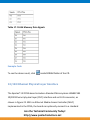
1
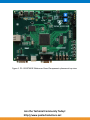
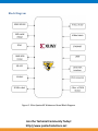
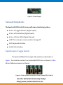
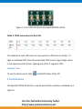
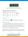
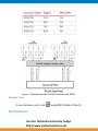
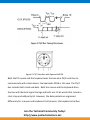
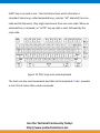
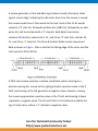
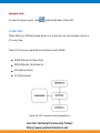
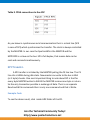
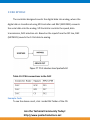
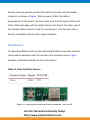
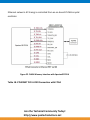
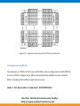
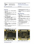
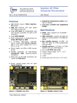
CPLD/FPGA BOARDS
Spartan 3E Webserver
Join the Technical Community Today!
http://www.pantechsolutions.net
Contents
Introduction .................................................................................................................... 3
1. Using Spartan3E FPGA Webserver Kit ....................................................................... 5
2. Learning Xilinx FPGA and ISE Development Software Basics ..................................... 6
Digital Inputs Toggle Switch ....................................................................................... 10
Light Emitting Diodes ................................................................................................. 11
5 Push Buttons ........................................................................................................... 12
RS-232 Serial Port ...................................................................................................... 13
PS/2 Interface ............................................................................................................ 14
VGA Display Port ........................................................................................................ 22
12 Bit ADC .................................................................................................................. 27
SPI Transfer. ............................................................................................................... 28
12 Bit SPI DAC ............................................................................................................ 29
JTAG Programming/Debugging Ports ......................................................................... 30
Clock Source .............................................................................................................. 31
SDRAM....................................................................................................................... 32
SDRAM Connections .................................................................................................. 33
FPGA-to-StrataFlash Connections ........................................................................... 36
10/100 Ethernet Physical Layer Interface .................................................................. 38
Spartan3e FPGA ......................................................................................................... 40
Configuration PROM .................................................................................................. 42
Join the Technical Community Today!
http://www.pantechsolutions.net
Introduction
The Spartan 3E TYRO Board provides a powerful and highly
advanced self-contained development platform for designs targeting the
Spartan 3E FPGA from Xilinx. It features a 500K gate Spartan 3E FPGA with a
32 bit RISC processor, SDRAM and FLASH interfaces. The board is fully
compatible with all versions of the Xilinx ISE tools including the free Web
Pack. The board ships with a power supply and Parallel JTAG cable for
programming, so designs can be implemented immediately with no hidden
costs
The board features:
Xilinx Spartan3E FPGA:
500,000-gate Xilinx Spartan 3E FPGA in a 208-PQFP (XC3S500EPQG208)
10476 logic cell equivalents
360 K-bit block RAMs
Twenty 18x18 hardware multipliers
Four Digital Clock Managers (DCMs)
Up to 158 user-defined I/O signals
Join the Technical Community Today!
http://www.pantechsolutions.net
External Peripherals Modules
4-Nos. General purpose point LEDs
4-Nos of Toggle switches (Digital inputs)
5-Nos of Push Button
PS/2 Keyboard or Mouse Interface
Communication protocols
Full Duplex UART (EIA RS232)
Other Features:
18 bit VGA Interface Connector
On-board 4 MB Platform Flash Memory (PROM)
16 MB On Board SDRAM
16 MB NOR FLASH Memory
JTAG Interface Connector for parallel programming
Spartan3E FPGA
50 MHz crystal oscillator clock source
Join the Technical Community Today!
http://www.pantechsolutions.net
Technical or Customer Support
Post your questions:
Pantech forum:
www.pantechsolutions.net/forum
Website :
www.pantechsolutions.net
1.
Using Spartan3E FPGA Webserver Kit
Package Contents
Xilinx Spartan3E XC3S500E FPGA Kit
Serial Port Cable (DTE)
JTAG Download Cable
Printed User Manual
5V Power AC Adaptor
CD contains
o Software
o Example Programs
o User Manual
o Simple Projects
Join the Technical Community Today!
http://www.pantechsolutions.net
2. Learning Xilinx FPGA and ISE Development
Software Basics
The Spartan-3E Board provides a powerful, self-contained
development platform for designs targeting the new Spartan-3E FPGA from
Xilinx. It features a 500K gate Spartan-3,on-board I/O devices, Ethernet,
16MB FLASH and 16MB SDRAM, making it the perfect platform to
experiment with any new design, from a simple logic circuit to an embedded
processor core. The board also contains a Platform Flash, JTAGprogrammable ROM, so designs can easily be made non-volatile.
Components placement
Join the Technical Community Today!
http://www.pantechsolutions.net
Figure 1. PS –SPARTAN3E Webserver Board Components placement top view
Join the Technical Community Today!
http://www.pantechsolutions.net
Block Diagram
Figure 2. Xilinx Spartan3E Webserver Board Block Diagram
Join the Technical Community Today!
http://www.pantechsolutions.net
Power Distribution
AC Wall Adapter
The Spartan3E FPGA Lab Kit includes an international-ready AC wall adapter
that produces a +5V DC output. Connect the AC wall adapter to the barrel connector
along the left edge of the board, indicated as in Figure 3. To disconnect power, switch
off the power switch. The power indicator LED, as shown in Figure 3, lights up when
power is properly applied to the board. The AC wall adapter operates from 100V to
240V AC input, at 50 or 60 Hz.
Voltage Regulators
There are Overall, the 5V DC switching power adapter that connects to AC
wall power powers the board. A 3.3V regulator, powered by the 5V DC supply,
provides power to the inputs of the 2.5V, 1.8V and 1.2V regulators. Similarly, the 3.3V
regulator feeds all the VCCO voltage supply inputs to the FPGA’s I/O banks and powers
most of the components on the board. The 2.5V regulator supplies power to the
FPGA’s VCCAUX supply inputs. The VCCAUX voltage input supplies power to Digital
Clock Managers (DCMs) within the FPGA and supplies some of the I/O structures. In
specific, all of the FPGA’s dedicated configuration pins, such as DONE, PROG_B, CCLK,
and the FPGA’s JTAG pins, are powered by VCCAUX. The FPGA configuration interface
on the board is powered by 3.3V. Consequently, the 2.5V supply has a current shunt
resistor to prevent reverse current. The supply 1.8V is for core voltage of LAN IC.
Finally, a 1.2V regulator supplies power to the FPGA’s VCCINT voltage inputs, which
power the FPGA’s core logic.
Join the Technical Community Today!
http://www.pantechsolutions.net
Figure 3. Power Supply
On-board Peripherals
The Spartan3E FPGA Lab Kit comes with many interfacing options
4-Nos. of Toggle switches (Digital Inputs)
5-Nos. of Push Button (Digital Inputs)
4-Nos. of Point LED’s (Digital Outputs)
UART for serial port communication through PC
PS/2 keyboard Interface
16-Bit VGA Interface
Digital Inputs Toggle Switch
The Spartan3FPGA Kit has eight slide switches, indicated as in
Figure . The switches connect to an associated FPGA pin, as shown in Table
1Error! Reference source not found.
Figure 4. Slide switches connections from Spartan3FPGA Lab Kit
Join the Technical Community Today!
http://www.pantechsolutions.net
Table 1. FPGA Connections to Slide Switches
When in the UP or ON position, a switch connects the FPGA pin to VCCO, a
logic High. When DOWN or in the OFF position, the switch connects the
FPGA pin to ground, a logic Low. The switches typically exhibit about 2 ms
of mechanical bounce and there is no active debouncing circuitry, although
such circuitry could easily be added to the FPGA design programmed on the
board. A 10KO series resistor provides nominal input protection.
Example Code
To see the demo result, click
inside Digital Input Switch folder of the
CD.
Light Emitting Diodes
Light Emitting Diodes (LEDs) are the most commonly us displaying pin’s
digital states. The Spartan3FPGA Lab K push button switches, indicated by in
Figure .
Join the Technical Community Today!
http://www.pantechsolutions.net
Figure 5. Point LED interface from Spartan3FPGA Lab Kit
Table 2. FPGA connections to the LEDs
The cathode of each LED connects to ground via a 220 ohm O resistor. To
light an individual LED, drive the associated FPGA control signal High, which
is the opposite polarity from lighting one of the 7-segment LEDs.
Example Code
To see the demo result, click
inside LED folder of the CD.
5 Push Buttons
The Spartan3 FPGA Kit has four contact push button switches, indicated as in
Figure 6.
Join the Technical Community Today!
http://www.pantechsolutions.net
Figure 6. Push Button interface from Spartan3 FPGA Kit
Table 3. FPGA Connections to Push Button
Example Code
To see the demo result, click
inside Push Button folder of the CD.
RS-232 Serial Port
The Spartan®-3E FPGA Starter Kit board has two RS-232 serial ports: a
female DB9 connector and a male DTE connector. The DCE-style port
connects directly to the connector available on most personal computers
and workstations via a standard through serial cable.
Table 4. RS232 signals and their pin assignments to the Spartan3e FPGA
Join the Technical Community Today!
http://www.pantechsolutions.net
Figure 7. Detailed schematic of FPGA Interface with RS232
Example Code
To see the demo result, click
inside RS232 folder of the CD.
PS/2 Interface
Join the Technical Community Today!
http://www.pantechsolutions.net
The Spartan3e FPGA Kit includes PS/2 port for mouse/keyboard
interface and it is the standard 6-pin mini-DIN connector, labeled U12 on
the board. Figure shows the PS/2 connector, and Table shows the signals
on the connector. Only pins 1 and 5 of the connector attach to the FPGA.
Table 5. PS/2 Interface with Spartan3eFPGA
Table 6. PS/2 Bus Timing
Join the Technical Community Today!
http://www.pantechsolutions.net
Figure 9. PS/2 Interface with Spartan3eFPGA
Both the PC mouse and the keyboard uses the two-wire PS/2 serial bus to
communicate with a host device, the Spartan3e FPGA in this case. The PS/2
bus includes both clock and data. Both the mouse and the keyboard drive
the bus with identical signal timings and both use 11-bit words that include a
start, stop and odd parity bit. However, the data packets are organized
differently for a mouse and keyboard. Furthermore, the keyboard interface
Join the Technical Community Today!
http://www.pantechsolutions.net
allows bidirectional data transfers so the host device can illuminate state
LEDs on the keyboard.
The PS/2 bus timing appears Table and Figure the clock and data signals
are only driven when data transfers occur; otherwise they are held in the
idle state at logic High. The timing defines signal requirements for mouse-tohost communications and bidirectional keyboard communications. As shown
in Figure , the attached keyboard or mouse writes a bit on the data line
when the clock signal is High, and the host reads the data line when the
clock signal is Low.
Keyboard
The keyboard uses open-collector drivers so that either the keyboard or the
host can drive the two-wire bus. If the host never sends data to the
keyboard, then the host can use simple input pins. A ps/2-style keyboard
uses scan-codes to communicate key press data. Nearly all keyboards in use
today are ps/2 style. Each key has a single, unique scan-code that is sent
whenever the corresponding key is pressed. The scan-codes for most keys
appear in Figure 1. If the key is pressed and held, the keyboard repeatedly
sends the scan-code every 100 ms or so. When a key is released, the
keyboard sends an “f0” key-up code, followed by the scan code of the
released key. The keyboard sends the same scan code, regardless if a key
has different SHIFT and non-SHIFT characters and regardless whether the
Join the Technical Community Today!
http://www.pantechsolutions.net
SHIFT key is pressed or not. The host determines which character is
intended. Some keys, called extended keys, send an “e0” ahead of the scancode and furthermore, they might send more than one scan code. When an
extended key is released, an “e0 f0” key-up code is sent, followed by the
scan code.
Figure 10. PS\2 style scan-code keyboard
The host can also send commands and data to the keyboard. Table provides
a short list of some often-used commands.
Join the Technical Community Today!
http://www.pantechsolutions.net
Table 7. Common PS/2 Keyboard Commands
Command
Description
ED
EE
F3
Turn on/off Num Lock, Caps Lock, and Scroll Lock LEDs
Echo. Upon receiving an echo command, t he keyboard replies
Set scan code repeat r at e. The keyboard acknowledges receipt of
an “F3” by returning an “FA”, after which the host sends a second
byte t o set t he repeat r ate.
Resend. Upon receiving a resend command, the keyboard resends t
he last scan code sent
Reset. Reset s t he keyboard
FE
FF
The keyboard sends commands or data to the host only when both the data
and clock lines are High, the Idle state, because the host is the bus master,
and the keyboard checks whether the host is sending data before driving the
bus. The clock line can be used as a clear to send signal. If the host pulls the
clock line Low, the keyboard must not send any data until the clock is
released. The keyboard sends data to the host in 11-bit words that contain a
‘0’ start bit, followed by eight bits of scan code (LSB first), followed by an
odd parity bit and terminated with a ‘1’ stop bit. When the keyboard sends
data, it generates 11 clock transitions at around 20 to 30 kHz, and data is
valid on the falling edge of the clock as shown in Figure .
Mouse
Join the Technical Community Today!
http://www.pantechsolutions.net
A mouse generates a clock and data signal when moved; otherwise, these
signals remain High, indicating the idle state. Each time the mouse is moved,
the mouse sends three 11-bit words to the host. Each of the 11-bit words
contains a ‘0’ start bit, followed by 8 data bits (LSB first), followed by an odd
parity bit, and terminated with a ‘1’ stop bit. Each data transmission
contains 33 total bits, where bits 0, 11, and 22 are ‘0’ start bits, and bits 10,
21, and 32 are ‘1’ stop bits. The three 8-bit data fields contain movement
data as shown in Figure . Data is valid at the falling edge of the clock, and the
clock period is 20 to 30 kHz.
A PS/2-style mouse employs a relative coordinate system (see Figure ),
wherein moving the mouse to the right generates a positive value in the X
field, and moving to the left generates a negative value. Likewise, moving
the mouse up generates a positive value in the Y field, and moving it down
represents a negative value. The XS and YS bits in the status byte define the
sign of each value, where a ‘1’ indicates a negative value.
Join the Technical Community Today!
http://www.pantechsolutions.net
Figure 13. The Mouse Uses a Relative Coordinate System to Track
Movement The magnitude of the X and Y values represent the rate of
mouse movement. The larger the value, the faster the mouse is moving. The
XV and YV bits in the status byte indicate when the X or Y values exceed
their maximum value, an overflow condition. A ‘1’ indicates when an
overflow occurs. If the mouse moves continuously, the 33-bit transmissions
repeats approximately every 50 ms. The L and R fields in the status byte
indicate Left and Right button presses. A ‘1’ indicates that the associated
mouse button is being pressed.
Example Code
To see the demo result, click inside PS/2 folder of the CD.
Join the Technical Community Today!
http://www.pantechsolutions.net
VGA Display Port
The Spartan3e FPGA Kit includes a VGA display port and DB15
connector, as indicated in Figure . You can connect this port directly to most
PC monitors or flat-panel LCD displays using a standard monitor cable.
As shown in Figure , the Spartan3eFPGA controls five VGA signals: Red
(R) its 1 pin in connector, Green (G) its 2 nd pin, Blue (B) its 3rd pin,
Horizontal Sync (HS) 13 pin, and Vertical Sync (VS) its 14 pin, all available on
the VGA connector. The FPGA pins that drive the VGA port appear in Table
8. A detailed schematic is in Figure 14.th
Join the Technical Community Today!
http://www.pantechsolutions.net
Table 8. FPGA connections to the VGA .
Signal s
Hori zont al Sync (Hs)
Ver t i cal Sync ( Vs)
Red1
Red2
Red3
Red4
Red5
Red6
Gr een1
Gr een2
Gr een3
Gr een4
Gr een5
Bl ue1
Bl ue2
Bl ue3
Bl ue4
Bl ue5
FPGAPIN
P180
P177
P181
P200
P193
P168
P163
P179
P181
P47
P42
P23
P45
P187
P185
P205
P113
P5
Each color line has a series resistor to provide 16-bit color, with six bit each
for Red, Green, and Blue. The series resistor uses the 75 ohm VGA cable
termination to ensure that the color signals remain in the VGA-specified 0V
to 0.7V range. The HS and VS signals are TTL level.
Join the Technical Community Today!
http://www.pantechsolutions.net
VGA signal timing is specified, published, copyrighted, and sold by the Video
Electronics Standards Association (VESA). The following VGA system and
timing information is provided as an example of how the FPGA might drive
VGA monitor in 640 by 480 modes. For more precise information or for
information on higher VGA frequencies, refer to documents available on the
VESA website or other electronics
Websites: Video Electronics Standards Association
http://www.vesa.org
VGA Timing Information
http://www.epanorama.net/documents/pc/vga_timing.html
Signal Timing for a 60Hz, 640x480 VGA Display
CRT-based VGA displays use amplitude-modulated, moving electron beams
to display information on a phosphor-coated screen. LCD displays use an
array of switches that can impose a voltage across a small amount of liquid
crystal, thereby changing light permittivity through the crystal on a pixel bypixel basis. Although the following description is limited to CRT displays, LCD
displays have evolved to use the same signal timings as CRT displays.
Consequently, the following discussion pertains to both CRTs and LCD
displays. Within a CRT display, current waveforms pass through the coils to
Join the Technical Community Today!
http://www.pantechsolutions.net
produce magnetic fields that deflect electron beams to transverse the
display surface in a “raster” pattern, horizontally from left to right and
vertically from top to bottom. As shown in Figure , information is only
displayed when the beam is moving in the “forward” direction—left to right
and top to bottom—and not during the time the beam returns back to the
left or top edge of the display. Much of the potential display time is
therefore lost in “blanking” periods when the beam is reset and stabilized to
begin a new horizontal or vertical display pass.
Figure 15. Illustration of the working of a VGA display
The size of the beams, the frequency at which the beam traces across the
display, and the frequency at which the electron beam is modulated
Join the Technical Community Today!
http://www.pantechsolutions.net
determine the display resolution. Modern VGA displays support multiple
display resolutions, and the VGA controller indicates the resolution by
producing timing signals to control the raster patterns. The controller
produces TTL-level synchronizing pulses that set the frequency at which
current flows through the deflection coils and it ensures that pixel or video
data is applied to the electron guns at the correct time. Video data typically
comes from a video refresh memory with one or more bytes assigned to
each pixel location. The controller indexes into the video data buffer as the
beams move across the display. The controller then retrieves and applies
video data to the display at precisely the time the electron beam is moving
across a given pixel. As shown in Figure , the VGA controller generates the
HS (horizontal sync) and VS (vertical sync) timings signals and coordinates
the delivery of video data on each ixel clock. The pixel clock defines the time
available to display one pixel of information. The VS signal defines the
“refresh” frequency of the display, or the frequency at which all information
on the display is redrawn. The minimum refresh frequency is a function of
the display’s phosphor and electron beam intensity, with practical refresh
frequencies in the 60 Hz to 120 Hz range. The number of horizontal lines
displayed at a given refresh frequency defines the horizontal “retrace”
frequency.
Join the Technical Community Today!
http://www.pantechsolutions.net
Example Code
To see the demo result, click
inside VGA folder of the CD.
12 Bit ADC
These ADCs are SPI Bus based which is a serial bus. So the number of pins in
IC is very low.
Total of 4 lines are required to interface it with FPGA.
MISO (Master In Slave Out)
MOSI (Master Out Slave In)
SCK (Serial Clock)
CS (Chip Select)
Figure 16. ADC interface from Spartan3e kit
Join the Technical Community Today!
http://www.pantechsolutions.net
Table 9. FPGA connections to the ADC
As you know in synchronous serial communication their is a clock line (SCK
in case of SPI) which synchronizes the transfer. The clock is always controlled
by the MASTER. In our case the Spartan3AN is the MASTER and the
MCP3202 is a slave on the bus. SPI is full duplex, that means data can be
sent and received simultaneously.
SPI Transfer.
A SPI transfer is initiated by the MASTER pulling the CS line low. The CS
line sits at HIGH during idle state. Now master can write to the bus in 8bit
(or 1 byte) chunks. One most important thing to note about SPI is that for
every byte MASTER writes to SLAVE the MASTER receives one byte in return.
So the only transaction possible is exchange of data. Their is no separate
Read and Write commands their is only one command and that is Write.
Example Code
To see the demo result, click inside ADC folder of the CD.
Join the Technical Community Today!
http://www.pantechsolutions.net
12 Bit SPI DAC
The controller designed coverts the digital data into analog, where the
digital data is transferred using SPI Controller and DAC (MCP4921) converts
the serial data into the analog. SPI Controller controls the speed, data
transmission, DAC selection etc. Based on the inputs from the SPI line, DAC
(MCP4921) coverts the 12 bit data to analog.
Table 10. FPGA connections to the DAC
Example Code
To see the demo result, click inside DAC folder of the CD.
Join the Technical Community Today!
http://www.pantechsolutions.net
JTAG Programming/Debugging Ports
The Spartan3e FPGA Lab kit includes a JTAG programming and
debugging chain. Additionally, there are two JTAG headers for driving the
JTAG signals from various supported JTAG download and debugging cables.
A PANTECH JTAG3 low-cost parallel to JTAG cable is included as part of the
kit and connects to the JTAG header. DB-25 parallel port connector connects
to the 6-pin female header connector. The JTAG cable connects directly to
the parallel port of a PC and to a standard 6-pin JTAG programming header
in the kit that can program a devices that have a JTAG voltage of 1.8v or
greater.
Figure 18. JTAG connection with Spartan3eFPGA
This JTAG header consists of 0.1-inch stake pins, located toward the top
edge of the board, directly below the two expansion connectors. The
Join the Technical Community Today!
http://www.pantechsolutions.net
Pantech low-cost parallel port to JTAG cable fits directly over the header
stake pins, as shown in Figure . When properly fitted, the cable is
perpendicular to the board. You must make sure that the signals at the end
of the JTAG cable align with the labels listed on the board. The other end of
the Pantech cable connects to the PC’s parallel port. The Pantech cable is
directly compatible with the Xilinx impact software.
Clock Source
The Spartan3eFPGA Lab Kit has two dedicated 50 MHz series clock oscillator
source and an optional socket for another clock oscillator source. Figure
provides a detailed schematic for the clock sources.
Table 11. Clock Oscillator Sources
Figure 19. Clock source connections from Spartan3eE FPGA Lab Kit
Join the Technical Community Today!
http://www.pantechsolutions.net
SDRAM
The Spartan®-3E FPGA boards includes a 128 Mbit (32M x 16) Micron
Technology DDR SDRAM (MT46V32M16) with a 16-bit data interface, as
shown in Figure. In general, the 128Mb SDRAMs (8 Meg x 4 x 4 banks, 4 Meg
x 8 x 4 banks and 2 Meg x 16 x 4 banks) are quadbank DRAMs that operate
at 3.3V and include a synchronous interface (all signals are registered on the
positive edge of the clock signal, CLK). Each of the x4’s 33,554,432- bit banks
is organized as 4,096 rows by 2,048 columns by 4 bits. Each of the x8’s
33,554,432-bit banks is organized as 4,096 rows by 1,024 columns by 8 bits.
Each of the x16’s 33,554,432-bit banks is organized as 4,096 rows by 512
columns by 16 bits.
Join the Technical Community Today!
http://www.pantechsolutions.net
Figure 20. SDRAM Interface with Spartan3E FPGA
SDRAM Connections
Table 12. SDRAM address bus connection with FPGA
Join the Technical Community Today!
http://www.pantechsolutions.net
Table 13. SDRAM Control Signals
Join the Technical Community Today!
http://www.pantechsolutions.net
Table 14. SDRAM Data Signals
Example Code
To see the demo result, click
inside SDRAM folder of the CD.
Intel StrataFlash Parallel NOR Flash PROM
Join the Technical Community Today!
http://www.pantechsolutions.net
The Spartan®-3E FPGA Starter Kit boards includes a 128 Mbit (16 Mbyte)
Intel StrataFlash parallel NOR Flash PROM. As indicated, some of the
StrataFlash connections are shared with other components on the board.
Figure 21. FLASH Memory Interface with Spartan3E FPGA
FPGA-to-StrataFlash Connections
Table 15. FLASH Memory address bus connection with FPGA
Signals
A0
A1
A2
FPGA Pins
P140
P138
P137
A3
P135
Join the Technical Community Today!
http://www.pantechsolutions.net
A4
P134
A5
P133
A6
P132
A7
P129
A8
P128
A9
P127
A10
P126
A11
P120
A12
P119
A13
P109
A14
P108
A15
P107
A16
P106
A17
A18
P102
P100
A19
A20
A21
A22
A22
A23
P99
P97
P96
P94
P93
P90
Table 16. FLASH Memory Control Signals
Join the Technical Community Today!
http://www.pantechsolutions.net
Table 17. FLASH Memory Data Signals
Example Code
To see the demo result, click
inside SDRAM folder of the CD.
10/100 Ethernet Physical Layer Interface
The Spartan®-3E FPGA board includes a Standard Microsystems LAN83C185
10/100 Ethernet physical layer (PHY) interface and an RJ-45 connector, as
shown in Figure 22. With an Ethernet Media Access Controller (MAC)
implemented in the FPGA, the board can optionally connect to a standard
Join the Technical Community Today!
http://www.pantechsolutions.net
Ethernet network. All timing is controlled from an on-board 25 MHz crystal
oscillator.
Figure 22. FLASH Memory Interface with Spartan3E FPGA
Table 18. ETHERNET PHY LAYER Connection with FPGA
Join the Technical Community Today!
http://www.pantechsolutions.net
Spartan3e FPGA
Introduction
The purpose of this daughter board is to integrate all the necessary
components for using a FPGA, but without being targeted on a special
application. The board provides 102 data pins to the user, who can use them
as inputs, outputs or both. The main component of the board is Spartan 3E
FPGA. The following figure elaborates the denotation.
Join the Technical Community Today!
http://www.pantechsolutions.net
Device Part Marking
The second important component on this board is the XCF04S-PROM, in
which you can store a bit-file. The FPGA can be programmed directly from
the PROM or through the JTAG connection. If the PROM-Boot option is
enabled, the FPGA will be programmed out of the PROM when the power is
turned on.
A general overview of the FPGA architecture is presented in the following
figure.
Join the Technical Community Today!
http://www.pantechsolutions.net
Figure 23. A general overview of the FPGA architecture
Configuration PROM
The Spartan-3 FPGA Lab Kit has an XCF04S serial configuration Flash PROM
to store FPGA configuration data and potentially additional non-volatile
data, including Micro Blaze application code.
Table 1. Pin description of Spartan3: XC3S200TQ144
Join the Technical Community Today!
http://www.pantechsolutions.net
JTAG OPTION
For most applications, this is the default jumper setting. As shown in
Figure , the Platform Flash is enabled only during configuration when the
FPGA’s DONE pin is Low. When the DONE pin goes high at the end of
configuration, the Platform Flash is disabled and placed in low-power mode.
Figure 24. Enabling JTAG Mode
NONE OPTION
If the JP3 jumper is removed, then the Platform Flash and FPGA are disabled.
Join the Technical Community Today!
http://www.pantechsolutions.net
PROG RST Push Button
The PROG RST push button forces the FPGA to reconfigure from the selected
configuration memory source. Press and release this button to restart the
FPGA configuration process at any time.
DONE Pin LED
The DONE pin LED lights whenever the FPGA is successfully configured. If
this LED is not lit, then the FPGA is not configured.
Join the Technical Community Today!
http://www.pantechsolutions.net
Did you enjoy the read?
Pantech solutions creates information packed
technical documents like this one every month. And
our website is a rich and trusted resource used by a
vibrant online community of more than 1,00,000
members from organization of all shapes and sizes.
Join the Technical Community Today!
http://www.pantechsolutions.net
What do we sell?
Our
products
range
from
Various
Microcontroller development boards, DSP Boards,
CPLD/CPLD boards, Communication Kits, Power
electronics, Basic electronics, Robotics, Sensors,
Electronic components and much more . Our goal is to
make finding the parts and information you need easier
and affordable so you can create awesome projects and
training from Basic to Cutting edge technology.
Join the Technical Community Today!
http://www.pantechsolutions.net