1
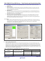
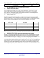
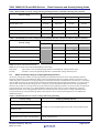
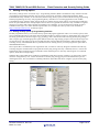
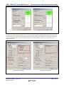
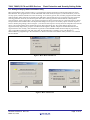
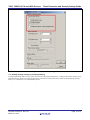
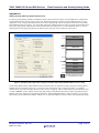
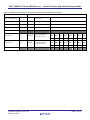
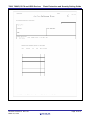
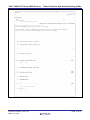
APPLICATION NOTE 78K0, 78K0R, RL78 and V850 Devices Flash Protection and Security Setting Guide R01AN1131EU0101 Rev.1.01 March 31, 2012 Introduction This application note provides a state-of-the-art protection of the Flash contents against a fraudulent readout of the flash contents of the 78K0, 78K0R, RL78 and V850 devices and a guide to security settings of aforementioned Renesas Electronics embedded flash Microcontrollers (MCUs). The application note first explains which protection features are provided in different access modes and afterward guides through how to achieve a specific protection level by setting security option. For specific device security settings, reference the microcontroller’s user manual, HEX Consolidation Utility user manual, PG-FP5 user manual and self-programming library application note for additional details. Contents 1. Protection Features ........................................................................................................................... 3 2. Security Option.................................................................................................................................. 5 3. Setting security option ....................................................................................................................... 9 Appendix A .............................................................................................................................................. 13 Appendix B .............................................................................................................................................. 15 R01AN1131EU0101 Rev.1.01 March 31, 2012 Page 1 of 21 78K0, 78K0R, RL78 and V850 Devices Flash Protection and Security Setting Guide List of Figures Figure 1 PG-FP5 Setup Windows....................................................................................................................................... 6 Figure 2 Main Window...................................................................................................................................................... 9 Figure 3 Device Setup Dialog Box .................................................................................................................................. 10 Figure 4 Security flag settings from target device ........................................................................................................... 10 Figure 5 HCU Main selection box................................................................................................................................... 11 Figure 6 HCU selection box ............................................................................................................................................ 11 Figure 7 HCU Option data dialog box............................................................................................................................. 12 Figure 8 Example of the option data settings in PG-FP5 and its Flash Shield Window memory map............................ 13 List of Tables Table 1. Relationship between flash shield window function and Commands.................................................................. 6 Table 2. Security protection level with Chip Erase function ............................................................................................. 7 Table 3. Relationship of security settings and Programming Interface commands with Chip Erase function ................... 8 Table 4. Relationship of security settings and Programming Interface commands without Chip Erase function ............. 8 Table 5. Relationship between security settings and self-programming............................................................................ 8 Table 6. Example of relationship between PG-FP5 setup and Option Release Form setting .......................................... 14 R01AN1131EU0101 Rev.1.01 March 31, 2012 Page 2 of 21 78K0, 78K0R, RL78 and V850 Devices 1. Flash Protection and Security Setting Guide Protection Features The protection of the Flash contents is achieved by implementing a whole range of features. There are different channels to access the Flash which needs to be considered independently: Flash Programming Interface, or the so called ‘Serial Programming Mode Debugging Interface Self-programming Mode Normal operation mode with instruction and data fetch from the flash The protection of each of the access types is described independently as those protection features are quite independent of each other. 1.1 Flash Programming Interface The Flash Programming Interface is active in the so called ‘Serial Programming Mode’ which allows the user to write to the internal flash memory of a virgin device or to reprogram a previously written device using an external programming tool. Those tools are either offered by Renesas Electronics, for example PG-FP5, or by 3rd parties. As this is a generic interface which could also be misused for read-out attacks, special care is taken to offer a proper protection of this interface. The following protection flags are available: − Chip Erase, where applicable − Block Erase − Program − Read, where applicable − Boot block cluster reprogramming The disabling of those programming interface functions will have the following effects: 1. Chip Erase The disabling of this function will prevent any erasure of the internal device flash by a flash programmer. Neither single blocks nor the entire flash can be erased. Thus it is not possible to update the stored memory contents with a flash programmer. As the self-programming operation is not influenced by this setting, it is possible to erase the flash memory in self-programming mode, and perform an application update. Please note that this function does not increase the protection against a read-out of the flash contents. This option should only be set if any reprogramming of the device with a flash programmer should be prevented. 2. Block Erase By disabling the block erase, it is not possible to erase single or multiple blocks of the flash memory. When block erase is disabled, only chip erase is possible. The disabling of the block erase ensures that it is only possible to erase the complete flash memory by chip erase if it is applicable. This ensures that no data remain in the device when performing an application update. Malicious software, which would be downloaded into the device with a flash programmer, will not be able to find remains of the old application. For some devices, it is impossible to erase the device after disabling block erase when chip erase function is not supported on that particular device. 3. Program Note By disabling program it is not possible to write any further data into the Flash memory. This feature prevents that a non-written area of the Flash is misused to store malicious software or to overwrite already written Flash areas with invalid data to cause software misbehavior. 4. Read Devices which offer a read command, also offer a flag to disable this command. 5. Boot block cluster reprogramming The disabling of this function will prevent any erasure of the internal device flash by a flash programmer and any erasure of the boot blocks by self-programming. Thus, the boot blocks will behave like as read only memory (ROM) after activating this function. Abovementioned security functions are also expressed as security flags such as Chip erase disable flag, Block erase disable flag, Write disable flag, Read disable flag, and Boot block cluster rewrite disable flag. Though different description among in documents, they are the same protection features. Section 2 will explain how to set these features for various protection levels. R01AN1131EU0101 Rev.1.01 March 31, 2012 Page 3 of 21 78K0, 78K0R, RL78 and V850 Devices Note: Flash Protection and Security Setting Guide For flash programming in this document, program and write are interchangeable jargons and so do the same as reprogram and rewrite. 1.2 Implementation of flags All above mentioned flags have no influence on the self-programming operations except Boot block cluster reprogramming. Even if the flags are set, all operation can be performed in the self-programming mode. Selfprogramming, nevertheless, cannot erase boot blocks when Boot block cluster reprogramming function is set. Example: When setting the block erase disable flag, single blocks cannot be erased via an external flash programming tool, but it is still possible to erase a single block, or a set of blocks, in the self-programming mode. The flags are implemented in such a way that the communication protocol rejects any command which is prohibited by the flags. Furthermore, the programming hardware itself is also configured by the flags in such a way that any operation which is prohibited by the flags is not possible. 1.3 Recommendation for usage of flags Out of those flags, the ‘Block Erase’, ‘Program’, and ‘Read’ flags are considered to be sufficient for an effective readout protection. The ‘Chip Erase’ and ‘Boot block cluster reprogramming’ disable prevents a reprogramming in serial mode completely and should therefore be used with care. 1.4 Debugging Interface For the debugging interface a 10 bytes password can be chosen which needs to be transmitted before the debugging interface can be used. For 32-bit device, V850 series, by setting the uppermost bit of this password to ‘0’ it is possible to disable the interface completely. For 8-bit and 16-bit devices, On-chip debug option byte setting will determine whether debug operation is enable or disable. This option byte setting can also be set for additional protection to erase flash content in case of authentication fail. 1.5 Self-programming The basic idea of self-programming is to write data, which are already available in the RAM of the device, to the Flash memory. Thus, the application needs the ability to receive those data from the outside. In order to provide the greatest flexibility, there is no limitation on the communication channel to receive those data. Consequently, it is not possible to provide a dedicated protection of those channels by Renesas Electronics, but partial protection can be done by Boot block cluster reprogramming and Flash Shield Window, which is explained in section 2.4. By setting Boot block cluster reprogramming function and/or Flash Shield Window, self-programming cannot reprogram specified flash memory area. It is up to the application program to ensure that those communication channels are not misused to gain an unwanted access to the flash and its contents. 1.6 Normal operation mode During normal operation mode no data which have been fetched from the internal memory can be observed from the outside. As some application offer diagnostic functions, it needs to be ensured that those diagnostic functions are properly protected against a misuse. 1.7 Considerations when using Flash protection flags - Potential influence on the Bootswap function of V850 devices The programming interface offers a single function to set the security flags. For V850 this command includes also a block number which is used either for the Boot cluster protection or for the Bootswap function. As this block number needs to be transmitted and as the original value of a blank device, which is 0xFF, is not possible, the activation of any security flag necessarily modifies the block number of the Bootswap function. 1.8 Low Pin Count device flash protection For RL78 low pin count 8-bit microcontroller such as RL78/G10, there has neither security flag nor self-programming functionality. This device can be checked blank only when shipped from factory. Once programmed the device, it can be erased and programmed by executing with single command – program after erase on entire flash memory. Thus, individual or a group of blocks erase and program are impossible. Since there is no security flag in this device, you cannot prohibit the device for reprogramming. Read and verify commands are not supported as well. R01AN1131EU0101 Rev.1.01 March 31, 2012 Page 4 of 21 78K0, 78K0R, RL78 and V850 Devices 2. Flash Protection and Security Setting Guide Security Option Using Renesas Electronics dedicated flash programmer PG-FP5 or third party programmer, application code in flash memory is secured by different levels of protection features. The security settings can also be set by self-programming and the explanation of detail setting using self-programming library will be described in respective User Manual. Using HEX Consolidation Utility software (HCU), the security settings can be merged with application code to single file and later utilized for factory programming. This section will explain on how to set these protections and their results of individual and combination of the setting. The following section will explain in detail on security option. Definition of Terms Security Settings Protection configuration settings 2.1 Definition of Terms − Application code Application code is an HEX file (i.e. program file) which is programmed without security option data into embedded flash memory. − [Erase] command The Erase command erases the flash memory in the target device. The erase command performs in two Operation modes: Chip mode and Block mode (refer to Figure 1[b]).The command erases all blocks in Chip mode and erases defined blocks only in Block mode. − [Program] command The Program command transmits the memory contents (program files) in the PG-FP5 valid programming area to the target device and writes the programs to the embedded flash memory. − [Read] command The Read command loads data on the embedded flash memory in the target device and saves it as a file. The read data can be saved in the Intel HEX format or Motorola HEX format − [Security] command The Security command sets the security functions (security settings) for the target device. − [Get Security settings] command The Get Security Settings command reads the setting of the security functions from the target device and displays the result in the PG-FP5 GUI. − ESF file ESF file (customized setup file) contains the programming environment settings specific to the user environment. This ESF file is generated by PG-FP5 programmer and not compatible to SET file generated by former programmer, PG-FP4. − HCUHEX file An HCUHEX file is created by HEX Consolidation Utility software for merging HEX files and option data. Note: The commands inside the closed bracket “[ ]” are executable by PG-FP5 programmer. This command symbol will be used throughout this document. 2.2 Security Settings Renesas Electronics microcontroller has five security functions and Flash Shield Window in embedded flash memory for protection. The following are description of each security and flash shield window function. I. Security function 1. 2. Disable Chip Erase Note 1 This security setting can prohibit erase command in Chip Operation mode (chip erase command) if it is applicable. Checked Disable Chip Erase box in Figure 3 [a], which selects as checked option, activates Chip erase disable flag and can prohibit erasing entire embedded flash memory. Disable Block Erase This security setting can prohibit erase command in Block Operation mode (Block erase command). Checked Disable Block Erase box in Figure 4[a], which selects as checked option, activates Block erase disable flag and R01AN1131EU0101 Rev.1.01 March 31, 2012 Page 5 of 21 78K0, 78K0R, RL78 and V850 Devices 3. 4. 5. Flash Protection and Security Setting Guide can prohibit erasing flash block via Programming Interface, but it does not affect on block erase by selfprogramming. Disable Program This security setting can prohibit program command. Checked Disable Program box in Figure 4[a], which selects as checked option, activates Program disable flag and can prohibit program command, but it allows reprogramming by self-programming. Disable Read Note 2 This security setting can prohibit read command via Programming Interface. Checked Disable Read box in Figure 4[a], which selects as checked option, activates Read disable flag and can prohibit reading data from embedded flash memory via Programming Interface. Disable Boot block cluster reprogramming This security setting can prohibit program command to boot blocks. Checked Disable Boot block cluster reprogramming box in Figure 4[a], which selects as checked option, activates Boot block cluster rewrite disable flag and can prohibit writing boot blocks. After setting this security function, self-programming can erase and write individual block except boot blocks. Note 1 and 2: Disable Chip Erase and Disable Read setting are only accessible on supported device. If the device does not support these features, Disable Chip Erase and Disable Read check boxes will dim in setup dialog box. Refer to specific device’s User Manual for a detailed description. For example, Figure 1 [c] shows these circumstances in Security flag setting group box. Figure 1 PG-FP5 Setup Windows II. Flash shield window function Flash shield window function can prevent writing and erasing flash memory area out of specified range in selfprogramming. The window, however, does not limit to Programming Interface command. The flash shield window range can be set or changed via start block and end block of flash memory either under Block protection area form programmer GUI (as shown in Figure 1[c], Block protection setting group box) or in self-programming mode. The relationship between flash shield window function and Programming Interface commands is shown in Table 1. This function can only be available on supported device. Table 1. Relationship between flash shield window function and Commands Programming Conditions Flash shield window range Self-programming Specify window range by selfprogramming library function Programming Interface Specify window range under R01AN1131EU0101 Rev.1.01 March 31, 2012 Command Block Erase Enable block erase within specified flash shield window range No effect on specified Program Enable program within specified flash shield window range No effect on specified Page 6 of 21 78K0, 78K0R, RL78 and V850 Devices Flash Protection and Security Setting Guide Block protection area in programmer GUI flash shield window range flash shield window range Note: Block protection area is only accessible on supported device. If the device does not support this feature, the FS Block end and FS Block start check boxes will dim in Block protection area. 2.3 Protection configuration settings Each security setting has different protection levels and one or more settings can be activated by selecting checked options in parallel to facilitate security functions. After selecting checked option to Disable Chip Erase box, the application code is impossible to update via Programming Interface; it is possible to write by self-programming, however. The effects of Programming Interface commands and self-programming by security setting are shown in Table 3, Table 4, and Table 5 respectively. Protection level, Interface commands and self-programming related to Security settings will be described in the following sections. 2.4 Security protection level Basically, protection level can be set as irreversible or reversible setting. Once set to protection level to irreversible setting, the security setting cannot be changed to its original state. In contrast, protection level reversible setting can be possible to alter all security settings to default state by executing chip erase command or security release command whichever supported by device. [Erase] command in Chip operation mode by PG-FP5 programming interface can alter all security settings to unchecked condition. The security protection level settings are shown in Table 2. Table 2. Security protection level with Chip Erase function Security Setting Disable Chip Erase (if applicable) Disable Boot block cluster reprogramming Disable Program Disable Block Erase Disable Read (if applicable) Description Protection Level Setting Impossible to erase chip after setting checked option Impossible to erase chip after setting checked option Irreversible Irreversible Impossible to program after setting checked option Impossible to erase block after setting checked option Impossible to read after setting checked option Reversible Reversible Reversible Note: It is only possible to restore the security setting to default state if all blocks are erased at once by [Erase] command in Chip operation mode. 2.5 Relationship between security settings and Programming Interface command Depending on security setting, programmer cannot execute any one or more of the Programming Interface commands. For example, by using the device that supports all security flag setting shown in Figure 4[a] and checking to Disable Program and Disable Block Erase boxes, programmer can execute [Erase] command and [Read] command only. If you also check to Disable Read box in previous setting, programmer can execute only [Erase] command. Any combination of security settings can be set for different protection levels. The relationship between security settings and Programming Interface commands with Chip Erase function is shown in Table 3, and the relationship without Chip Erase function is shown in Table 4. Block erase function is used for erasing all blocks when [Erase] command is used in PG-FP5 programmer if there is no chip erase function. The programmer cannot support [Read] command to 8-bit and 16-bit MCU such as 78K0, 78K0R, and RL78 device because read function is not applicable to those devices. Thus, Security setting for Disable Read is conditionally applicable in Table 3 and Table 4. For specific relationship between security settings and Programming Interface commands, refer to respective device’s User Manual for additional details. R01AN1131EU0101 Rev.1.01 March 31, 2012 Page 7 of 21 78K0, 78K0R, RL78 and V850 Devices Flash Protection and Security Setting Guide Table 3. Relationship of security settings and Programming Interface commands with Chip Erase function Programming Interface command Security setting Chip erase Block erase Program Read Disable Chip erase Impossible Impossible Possible Possible Disable Block erase Possible Impossible Possible Possible Disable Program Possible Impossible Impossible Possible Disable Read (if applicable) Possible Possible Possible Impossible Disable Boot block cluster reprogramming Impossible Possible Note1 Possible Note1 Possible Table 4. Relationship of security settings and Programming Interface commands without Chip Erase function Programming Interface command Security setting Block erase Program Read Impossible Possible Note2 Possible Disable Program Possible Impossible Possible Disable Read (if applicable) Possible Possible Impossible Possible Note1 Possible Note1 Possible Chip erase Disable Chip erase Disable Block erase Disable Boot block cluster reprogramming Note1: All blocks other than boot blocks. Note2: Only for blank blocks after disabling Block erase setting. Impossible : Impossible to execute Programming Interface command after setting checked option Possible : Possible to execute Programming Interface command after setting checked option 2.6 Effect of security setting on self-programming functions All security settings do not affect on self-programming except Disable Boot block cluster reprogramming function. Selecting checked option to Disable Boot block cluster reprogramming function prohibits erasing boot blocks so that neither chip erase command nor self-programming can erase the boot blocks. Disable Block erase function, nevertheless, does not affect on blocks except boot blocks for both Programming Interface and self-programming. If you select block option button inside Operation mode group box in Figure 1 [b], checking Disable Boot block cluster reprogramming function will not affect on erasing blocks except boot blocks by Programming Interface. If the device has not supported Chip Erase function (see Figure 1 [c], dimmed Disable Chip Erase check box), the same configuration, checking Disable Boot block cluster reprogramming function as abovementioned, will not affect on erasing individual block except boot blocks by self-programming. Refer to the respective device self-programming library User Manual for detailed description. Table 5. Relationship between security settings and self-programming Security setting Self-programming function Disable Chip erase (if applicable) Disable Block erase No effect on self-programming functions after setting checked option Disable Program Disable Read (if applicable) Disable Boot block cluster reprogramming R01AN1131EU0101 Rev.1.01 March 31, 2012 Effect on block erase and write functions to boot block clusters after setting checked option. Page 8 of 21 78K0, 78K0R, RL78 and V850 Devices 3. Flash Protection and Security Setting Guide Setting security option The security settings can be set in three ways – Programming Interface, HEX Consolidation Utility software and selfprogramming. Programming Interface can set security option using on-board or off-board programming. HEX Consolidation Utility software, on the other hand, allows setting security option in edit mode for factory programming and self-programming can set by self-programming library when device is executing application code. If HEX Consolidation Utility software cannot support the device, manual security setting will be processed with printed form known as Option Release Form. Sample Option form is shown in Appendix B. The form is only available on regional support up on request and contact regional representative for availability. In case of online File Transfer System is available in that region, use online instead of printed form. For example, the online system can be available at https://romcode.renesas.eu/rcts/ for Europe region. 3.1 Setting security option by Programming Interface PG-FP5 programmer allows you to set the security option and program application code. To set security option, select setup command under Device pull-down menu from Main window as shown in Figure 2. Setup Dialog box will prompt for setting option data as shown in Figure 1 [a], [b] and [c]. Select Advanced Tab for selecting Security flag settings – refer to Figure 3[a]. Checked appropriate option buttons in Security flag settings group box will activate the respective security functions. The setting will be saved in ESF file after clicking OK button and back to Main Window. Either executing security command under Device pull-down menu or clicking security icon will program the option data to embedded flash memory. Since option data is set differently from Application code, it cannot be written by Program command. Alternatively, executing Program command does not program the Security flag settings. Security command, however, will execute automatically after executing Program command if select checked option to “Security after Program” in Command options, which shown in Figure 4[a]. When the HCU object HEX file is loaded for programming to PG-FP5 as shown in Figure 3 [b], the security setting cannot be configurable by user. All the check boxes in Security flag setting group box will be dimmed to prevent checking the boxes. This circumstance of loading with HCU object HEX file shows in Figure 4 [b] for Security flag setting. Figure 2 Main Window R01AN1131EU0101 Rev.1.01 March 31, 2012 Page 9 of 21 78K0, 78K0R, RL78 and V850 Devices [a] Load with object HEX file Flash Protection and Security Setting Guide [b] Load with HCU object HEX file Figure 3 Device Setup Dialog Box For retrieving security option from target device, select Get Security Settings command under Device pull-down menu and Setup dialog box will prompt with programmed Security flag settings. In this dialog box, clicking OK button will store up-loaded option data to ESF file and revise the previous setting. Refer to PG-FP5 User Manual for a more detailed description. Figure 4 Security flag settings from target device R01AN1131EU0101 Rev.1.01 March 31, 2012 Page 10 of 21 78K0, 78K0R, RL78 and V850 Devices Flash Protection and Security Setting Guide 3.2 Setting security by HEX consolidation utility HEX Consolidation Utility software (HCU) is a program that combines application code and option data into single HCUHEX file. This program has two modes: Edit mode and Check mode (see Figure 5). Edit mode allows you to set security option, and Check mode can review the setting. To set security option, first, run HCU program and select Edit mode from HCU Main selection box and then click OK button. Second selection box (see Figure 6[a]) will prompt for selecting parameter meter file, hex file and option data. After selecting parameter file and hex file, clicking third selection button “Select Option data”, will prompt a message box shown in Figure 6[b] for option data selection. Select Set Option data and click OK button. The Option data dialog box will open to set security option. Checked respective boxes in Security flag settings, shown in Figure 7, will activate the respective security functions. Depend on the selected device, only supported flag can be checked in Security flag setting group box. The option buttons which are not supported security flags in this group box will dimed. In the Figure 7, Disable Chip Erase and Disable Read are not supported in this case. Finally, click OK buttons to generate consolidated HCUHEX file and ready for programming. After consolidating application code and option data, the HCUHEX file is needed to verify with PG-FP5 or MINICUBE2® by programming to the selected device. Refer to the HEX Consolidation Utility software User Manual for more details. Figure 5 HCU Main selection box Figure 6 HCU selection box R01AN1131EU0101 Rev.1.01 March 31, 2012 Page 11 of 21 78K0, 78K0R, RL78 and V850 Devices Flash Protection and Security Setting Guide Figure 7 HCU Option data dialog box 3.3 Setting security settings by self-programming In self-programming mode, security option can be set by self-programming library. Using specific library function calls, individual security function can be activated, but it cannot be reversed by the library. Refer to self flash programming library User Manual for a more detailed description. R01AN1131EU0101 Rev.1.01 March 31, 2012 Page 12 of 21 78K0, 78K0R, RL78 and V850 Devices Flash Protection and Security Setting Guide Appendix A Setting security option by Option Release Form For factory programming, if HEX Consolidation Utility software does not support to an intended device, manual entry will be used for setting security option. In this case, Renesas Electronics will issue an Option Release Form for each Application code. A sample Option Release Form is shown Appendix B. Follow the specific instructions on provided Option Release Form for accuracy. For option data setting, the sample form has a couple of groups list from 002 to 005 for Security flag settings and from 007 to 022 for Block protection. Mark with “01” for unchecked option or “02” for checked option in the appropriate bracket to deactivate or activate the security functions respectively. 3FFFFH Block 127 3F800H ≈ ≈ 3C800H Block 120 3B800H ≈ ≈ 02000H Block 3 01000H 00800H 00000H Block 2 Block 1 Block 0 Rewrite prohibit memory area in self-programming mode Figure 8 Example of the option data settings in PG-FP5 and its Flash Shield Window memory map In the Option Release Form, flash shield block start and end values are expressed in binary format for selecting block number. Set bit to one with writing “01” or reset bit to zero with writing “02” in respective bracket. As a sample demonstration, option data setting in PG-FP5 setup is shown in Figure 8, and its related setting to Option Release form is listed in Table 6 . In this example, the Security flag settings permit Disable Boot block cluster reprogramming and Disable Chip erase command via Programming Interface. The Flash Shield Window setting also allows you to rewrite flash memory from 1800H (start address of block 3) to 3C7FFH (end address of block 120) in self-programming mode. R01AN1131EU0101 Rev.1.01 March 31, 2012 Page 13 of 21 78K0, 78K0R, RL78 and V850 Devices Flash Protection and Security Setting Guide Table 6. Example of relationship between PG-FP5 setup and Option Release Form setting PG-FP5 Option Release Form Disable Boot block cluster reprogramming unchecked 002 Disabling rewriting boot cluster 0 flag [01] enabled boot block cluster 0 rewriting Disable Block erase checked 003 Disabling block erase flag [02] disabled block erase Disable Chip erase unchecked 004 Disabling batch erase flag [01] Disable Program checked 005 Disabling write flag [02] 007-014 Flash Shield Window start block (binary) enabled batch erase “chip erase” disabled write Disable Read FS Block start FS Block end 3 120 015-022 Flash Shield Window start block (binary) (007) (008) (009) (010) (011) (012) (013) (014) Bit-7 Bit-6 Bit-5 Bit-4 Bit-3 Bit-2 Bit-1 Bit-0 [02] [02] [02] [02] [02] [02] [01] [01] (015) (016) (017) (018) (019) (020) (021) (022) Bit-7 Bit-6 Bit-5 Bit-4 Bit-3 Bit-2 Bit-1 Bit-0 [02] [01] [01] [01] [01] [02] [02] [02] Boot Block end R01AN1131EU0101 Rev.1.01 March 31, 2012 Page 14 of 21 78K0, 78K0R, RL78 and V850 Devices Flash Protection and Security Setting Guide Appendix B Sample Option Release Form R01AN1131EU0101 Rev.1.01 March 31, 2012 Page 15 of 21 78K0, 78K0R, RL78 and V850 Devices R01AN1131EU0101 Rev.1.01 March 31, 2012 Flash Protection and Security Setting Guide Page 16 of 21 78K0, 78K0R, RL78 and V850 Devices R01AN1131EU0101 Rev.1.01 March 31, 2012 Flash Protection and Security Setting Guide Page 17 of 21 78K0, 78K0R, RL78 and V850 Devices R01AN1131EU0101 Rev.1.01 March 31, 2012 Flash Protection and Security Setting Guide Page 18 of 21 78K0, 78K0R, RL78 and V850 Devices R01AN1131EU0101 Rev.1.01 March 31, 2012 Flash Protection and Security Setting Guide Page 19 of 21 78K0, 78K0R, RL78 and V850 Devices R01AN1131EU0101 Rev.1.01 March 31, 2012 Flash Protection and Security Setting Guide Page 20 of 21 78K0, 78K0R, RL78 and V850 Devices Flash Protection and Security Setting Guide Renesas Electronics Website http://www.renesas.com/ Inquiries http://www.renesas.com/inquiry All trademarks and registered trademarks are the property of their respective owners. R01AN1131EU0101 Rev.1.01 March 31, 2012 Page 21 of 21 Revision Record Rev. 1.01 Date March 31, 2012 Description Page Summary — First edition issued A-1 General Precautions in the Handling of MPU/MCU Products The following usage notes are applicable to all MPU/MCU products from Renesas. For detailed usage notes on the products covered by this manual, refer to the relevant sections of the manual. If the descriptions under General Precautions in the Handling of MPU/MCU Products and in the body of the manual differ from each other, the description in the body of the manual takes precedence. 1. Handling of Unused Pins Handle unused pins in accord with the directions given under Handling of Unused Pins in the manual. ⎯ The input pins of CMOS products are generally in the high-impedance state. In operation with an unused pin in the open-circuit state, extra electromagnetic noise is induced in the vicinity of LSI, an associated shoot-through current flows internally, and malfunctions occur due to the false recognition of the pin state as an input signal become possible. Unused pins should be handled as described under Handling of Unused Pins in the manual. 2. Processing at Power-on The state of the product is undefined at the moment when power is supplied. ⎯ The states of internal circuits in the LSI are indeterminate and the states of register settings and pins are undefined at the moment when power is supplied. In a finished product where the reset signal is applied to the external reset pin, the states of pins are not guaranteed from the moment when power is supplied until the reset process is completed. In a similar way, the states of pins in a product that is reset by an on-chip power-on reset function are not guaranteed from the moment when power is supplied until the power reaches the level at which resetting has been specified. 3. Prohibition of Access to Reserved Addresses Access to reserved addresses is prohibited. ⎯ The reserved addresses are provided for the possible future expansion of functions. Do not access these addresses; the correct operation of LSI is not guaranteed if they are accessed. 4. Clock Signals After applying a reset, only release the reset line after the operating clock signal has become stable. When switching the clock signal during program execution, wait until the target clock signal has stabilized. ⎯ When the clock signal is generated with an external resonator (or from an external oscillator) during a reset, ensure that the reset line is only released after full stabilization of the clock signal. Moreover, when switching to a clock signal produced with an external resonator (or by an external oscillator) while program execution is in progress, wait until the target clock signal is stable. 5. Differences between Products Before changing from one product to another, i.e. to one with a different type number, confirm that the change will not lead to problems. ⎯ The characteristics of MPU/MCU in the same group but having different type numbers may differ because of the differences in internal memory capacity and layout pattern. When changing to products of different type numbers, implement a system-evaluation test for each of the products. Notice 1. All information included in this document is current as of the date this document is issued. Such information, however, is subject to change without any prior notice. Before purchasing or using any Renesas Electronics products listed herein, please confirm the latest product information with a Renesas Electronics sales office. Also, please pay regular and careful attention to additional and different information to be disclosed by Renesas Electronics such as that disclosed through our website. 2. Renesas Electronics does not assume any liability for infringement of patents, copyrights, or other intellectual property rights of third parties by or arising from the use of Renesas Electronics products or technical information described in this document. No license, express, implied or otherwise, is granted hereby under any patents, copyrights or other intellectual property rights of Renesas Electronics or others. 3. You should not alter, modify, copy, or otherwise misappropriate any Renesas Electronics product, whether in whole or in part. 4. Descriptions of circuits, software and other related information in this document are provided only to illustrate the operation of semiconductor products and application examples. You are fully responsible for the incorporation of these circuits, software, and information in the design of your equipment. Renesas Electronics assumes no responsibility for any losses incurred by you or third parties arising from the use of these circuits, software, or information. 5. When exporting the products or technology described in this document, you should comply with the applicable export control laws and regulations and follow the procedures required by such laws and regulations. You should not use Renesas Electronics products or the technology described in this document for any purpose relating to military applications or use by the military, including but not limited to the development of weapons of mass destruction. Renesas Electronics products and technology may not be used for or incorporated into any products or systems whose manufacture, use, or sale is prohibited under any applicable domestic or foreign laws or regulations. 6. Renesas Electronics has used reasonable care in preparing the information included in this document, but Renesas Electronics does not warrant that such information is error free. Renesas Electronics 7. Renesas Electronics products are classified according to the following three quality grades: "Standard", "High Quality", and "Specific". The recommended applications for each Renesas Electronics product assumes no liability whatsoever for any damages incurred by you resulting from errors in or omissions from the information included herein. depends on the product's quality grade, as indicated below. You must check the quality grade of each Renesas Electronics product before using it in a particular application. You may not use any Renesas Electronics product for any application categorized as "Specific" without the prior written consent of Renesas Electronics. Further, you may not use any Renesas Electronics product for any application for which it is not intended without the prior written consent of Renesas Electronics. Renesas Electronics shall not be in any way liable for any damages or losses incurred by you or third parties arising from the use of any Renesas Electronics product for an application categorized as "Specific" or for which the product is not intended where you have failed to obtain the prior written consent of Renesas Electronics. The quality grade of each Renesas Electronics product is "Standard" unless otherwise expressly specified in a Renesas Electronics data sheets or data books, etc. "Standard": Computers; office equipment; communications equipment; test and measurement equipment; audio and visual equipment; home electronic appliances; machine tools; personal electronic equipment; and industrial robots. "High Quality": Transportation equipment (automobiles, trains, ships, etc.); traffic control systems; anti-disaster systems; anti-crime systems; safety equipment; and medical equipment not specifically designed for life support. "Specific": Aircraft; aerospace equipment; submersible repeaters; nuclear reactor control systems; medical equipment or systems for life support (e.g. artificial life support devices or systems), surgical implantations, or healthcare intervention (e.g. excision, etc.), and any other applications or purposes that pose a direct threat to human life. 8. You should use the Renesas Electronics products described in this document within the range specified by Renesas Electronics, especially with respect to the maximum rating, operating supply voltage range, movement power voltage range, heat radiation characteristics, installation and other product characteristics. Renesas Electronics shall have no liability for malfunctions or damages arising out of the use of Renesas Electronics products beyond such specified ranges. 9. Although Renesas Electronics endeavors to improve the quality and reliability of its products, semiconductor products have specific characteristics such as the occurrence of failure at a certain rate and malfunctions under certain use conditions. Further, Renesas Electronics products are not subject to radiation resistance design. Please be sure to implement safety measures to guard them against the possibility of physical injury, and injury or damage caused by fire in the event of the failure of a Renesas Electronics product, such as safety design for hardware and software including but not limited to redundancy, fire control and malfunction prevention, appropriate treatment for aging degradation or any other appropriate measures. Because the evaluation of microcomputer software alone is very difficult, please evaluate the safety of the final products or system manufactured by you. 10. Please contact a Renesas Electronics sales office for details as to environmental matters such as the environmental compatibility of each Renesas Electronics product. Please use Renesas Electronics products in compliance with all applicable laws and regulations that regulate the inclusion or use of controlled substances, including without limitation, the EU RoHS Directive. Renesas Electronics assumes no liability for damages or losses occurring as a result of your noncompliance with applicable laws and regulations. 11. This document may not be reproduced or duplicated, in any form, in whole or in part, without prior written consent of Renesas Electronics. 12. Please contact a Renesas Electronics sales office if you have any questions regarding the information contained in this document or Renesas Electronics products, or if you have any other inquiries. (Note 1) "Renesas Electronics" as used in this document means Renesas Electronics Corporation and also includes its majority-owned subsidiaries. (Note 2) "Renesas Electronics product(s)" means any product developed or manufactured by or for Renesas Electronics. http://www.renesas.com SALES OFFICES Refer to "http://www.renesas.com/" for the latest and detailed information. Renesas Electronics America Inc. 2880 Scott Boulevard Santa Clara, CA 95050-2554, U.S.A. Tel: +1-408-588-6000, Fax: +1-408-588-6130 Renesas Electronics Canada Limited 1101 Nicholson Road, Newmarket, Ontario L3Y 9C3, Canada Tel: +1-905-898-5441, Fax: +1-905-898-3220 Renesas Electronics Europe Limited Dukes Meadow, Millboard Road, Bourne End, Buckinghamshire, SL8 5FH, U.K Tel: +44-1628-585-100, Fax: +44-1628-585-900 Renesas Electronics Europe GmbH Arcadiastrasse 10, 40472 Düsseldorf, Germany Tel: +49-211-65030, Fax: +49-211-6503-1327 Renesas Electronics (China) Co., Ltd. 7th Floor, Quantum Plaza, No.27 ZhiChunLu Haidian District, Beijing 100083, P.R.China Tel: +86-10-8235-1155, Fax: +86-10-8235-7679 Renesas Electronics (Shanghai) Co., Ltd. Unit 204, 205, AZIA Center, No.1233 Lujiazui Ring Rd., Pudong District, Shanghai 200120, China Tel: +86-21-5877-1818, Fax: +86-21-6887-7858 / -7898 Renesas Electronics Hong Kong Limited Unit 1601-1613, 16/F., Tower 2, Grand Century Place, 193 Prince Edward Road West, Mongkok, Kowloon, Hong Kong Tel: +852-2886-9318, Fax: +852 2886-9022/9044 Renesas Electronics Taiwan Co., Ltd. 13F, No. 363, Fu Shing North Road, Taipei, Taiwan Tel: +886-2-8175-9600, Fax: +886 2-8175-9670 Renesas Electronics Singapore Pte. Ltd. 1 harbourFront Avenue, #06-10, keppel Bay Tower, Singapore 098632 Tel: +65-6213-0200, Fax: +65-6278-8001 Renesas Electronics Malaysia Sdn.Bhd. Unit 906, Block B, Menara Amcorp, Amcorp Trade Centre, No. 18, Jln Persiaran Barat, 46050 Petaling Jaya, Selangor Darul Ehsan, Malaysia Tel: +60-3-7955-9390, Fax: +60-3-7955-9510 Renesas Electronics Korea Co., Ltd. 11F., Samik Lavied' or Bldg., 720-2 Yeoksam-Dong, Kangnam-Ku, Seoul 135-080, Korea Tel: +82-2-558-3737, Fax: +82-2-558-5141 © 2012 Renesas Electronics Corporation. All rights reserved. Colophon 1.1