1
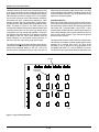
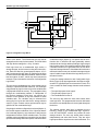
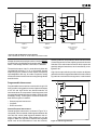
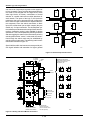
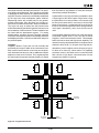
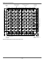
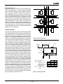
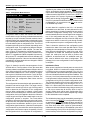
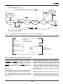
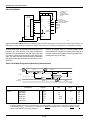
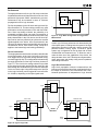
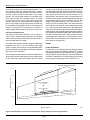
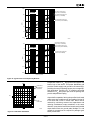
XC2000 Logic Cell Array Families Product Description Features • Fully Field-Programmable: – I/O functions – Digital logic functions – Interconnections • General-purpose array architecture • Complete user control of design cycle • Compatible arrays with logic cell complexity equiva- Device VCC XC2064 XC2064L XC2018 XC2018L 5.0 V 3.3 V 5.0 V 3.3 V Typ. Logic Capacity (gates) 600 – 1,000 600 – 1,000 1,000 - 1,500 1,000 - 1,500 CLBs User I/O Max Config. bits 64 64 100 100 58 58 74 74 12,038 12,038 17,878 17,878 The XC2000 family operates with a nominal 5.0 V supply. The XC2000L family operates with nominal 3.3 V supply. lent from 600 to 1,500 gates • • • • • • • The LCA logic functions and interconnections are determined by data stored in internal static-memory cells. Onchip logic provides for automatic loading of configuration data at power-up. The program data can reside in an EEPROM, EPROM or ROM on the circuit board or on a floppy disk or hard disk. The program can be loaded in a number of modes to accommodate various system requirements. Available in 5-V and 3.3-V versions 100% factory tested Selectable configuration modes Low-power, CMOS, static-memory technology Performance equivalent to TTL SSI/MSI TTL or CMOS input thresholds Architecture Complete development system support – XACT Design Editor – Schematic Entry – Macro Library – Timing Calculator – Logic and Timing Simulator – Auto Place / Route Description The Logic Cell Array (LCA) is a high density CMOS integrated circuit. Its user-programmable array architecture is made up of three types of configurable elements: Input/Output Blocks, logic blocks and Interconnect. The designer can define individual I/O blocks for interface to external circuitry, define logic blocks to implement logic functions and define interconnection networks to compose larger scale logic functions. The XACT Development System provides interactive graphic design capture and automatic routing. Both logic simulation and in-circuit emulation are available for design verification. The Logic Cell Array is available in a variety of logic capacities, package styles, temperature ranges and speed grades. The general structure of a Logic Cell Array is shown in Figure 1. The elements of the array include three categories of user programmable elements: I/O Blocks (IOBs), Configurable Logic Blocks (CLBs) and Programmable Interconnections. The I/OBs provide an interface between the logic array and the device package pins. The CLBs perform user-specified logic functions, and the interconnect resources are programmed to form networks that carry logic signals among the blocks. LCA configuration is established through a distributed array of memory cells.The XACT development system generates the program used to configure the Logic Cell Array which includes logic to implement automatic configuration. Configuration Memory The configuration of the Logic Cell Array is established by programming memory cells which determine the logic functions and interconnections. The memory loading process is independent of the user logic functions. 2-187