1
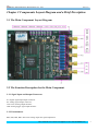
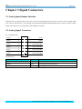
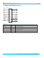
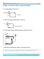
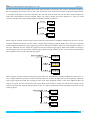
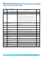
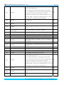
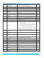
ART2750
User’s Manual
Beijing ART Technology Development Co., Ltd.
Beijing ART Technology Development Co., Ltd.
V6.1.18
Contents
Contents ................................................................................................................................................................................2
Chapter 1 Overview ..............................................................................................................................................................3
Chapter 2 Components Layout Diagram and a Brief Description .......................................................................................5
2.1 The Main Component Layout Diagram ..................................................................................................................5
2.2 The Function Description for the Main Component ...............................................................................................5
2.2.1 Signal Input and Output Connectors ............................................................................................................5
2.2.2 Potentiometer ...............................................................................................................................................5
2.2.3 Jumper..........................................................................................................................................................6
2.2.4 Board Base Address Selection .....................................................................................................................6
2.2.5 Indicator .......................................................................................................................................................6
Chapter 3 Signal Connectors.................................................................................................................................................7
3.1 Analog Input/Output Interface ................................................................................................................................7
3.2 Analog Signal Connector ........................................................................................................................................7
3.3 Digital Input/Output Connector ..............................................................................................................................8
Chapter 4 Connection Ways for Input and Output................................................................................................................9
4.1 Analog Output Connection......................................................................................................................................9
4.2 External Trigger Signal (ART) Connection ............................................................................................................9
4.3 Clock input/Output and Digital Trigger Signal Connection....................................................................................9
4.4 Methods of Realizing the Multi-card Synchronization ...........................................................................................9
Chapter5 Address Allocation Table.....................................................................................................................................11
Chapter 6 Notes and Warranty Policy ................................................................................................................................14
6.1 Notes .....................................................................................................................................................................14
6.2 Analog Signal Output Calibration.........................................................................................................................14
8.3 Warranty Policy.....................................................................................................................................................14
Products Rapid Installation and Self-check ........................................................................................................................16
Rapid Installation ........................................................................................................................................................16
Self-check ...................................................................................................................................................................16
Delete Wrong Installation ...........................................................................................................................................16
BUY ONLINE at art-control.com/englishs or CALL+86-10-51289836(CN)
2
Beijing ART Technology Development Co., Ltd.
V6.1.18
Chapter 1 Overview
ART2750 is an arbitrary waveform generator card based on PC104 bus, can be connected to the computer's PC104
interface to constitute the laboratory, product quality inspection center and other areas of data acquisition, waveform
analysis and processing system. And also can constitute industrial process monitoring system. Its main applications are:
■ Electronic Product Quality Testing
■ Signal acquisition
■ Process Control
■ Servo Control
Unpacking Checklist
Check the shipping carton for any damage. If the shipping carton and contents are damaged, notify the local dealer or
sales for a replacement. Retain the shipping carton and packing material for inspection by the dealer.
Check for the following items in the package. If there are any missing items, contact your local dealer or sales.
¾ Art2750 Data Acquisition Board
¾ ART Disk
a) user’s manual (pdf)
b) drive
c) catalog
¾ Warranty Card
DA Arbitrary Waveform Output Function
¾
¾
¾
¾
¾
¾
¾
¾
¾
¾
¾
¾
¾
¾
¾
¾
¾
Converter Type: AD7845
Output Range: 0~10V, ±5V, ±10V
Resolution: 12-bit
Output Point Rate (Frequency): up to 1MHz (1us/point). software adjustable, adjustable range: 0.01Hz ~ 1MHz
Analog Signal Bandwidth: 0~50KHz
Number of Channels: 4
Output Impedance: 50Ω or 75Ω (jumper setting)
Trigger Source: software independent trigger source, software synchronization trigger source, hardware analog
trigger source (ATR), hardware digital trigger source (DTR)
Trigger Level: ±10V (software setting)
Trigger Direction (TriggerDir): negative trigger, positive trigger, either positive or negative trigger
Clock Source: internal clock and external clock (CLINK) (software selectable)
Memory Depth: 1M word (point) RAM Memory
Work Flag: DA conversion flag, trigger flag, the current segment number, the current segment address, the current
segment number of cycles, the current total number of cycles
Data Transmission: program mode
Gain : 1time and 2 times
DA Set-up Time: ≤600ns
Non-linear Error: 0.5LSB
BUY ONLINE at art-control.com/englishs or CALL+86-10-51289836(CN)
3
Beijing ART Technology Development Co., Ltd.
V6.1.18
Other Features
¾
¾
On-board Clock Oscillator: 40MHz
Dimension: 102mm (L) * 127mm (W) * 16mm (H)
102mm (L) * 135mm (W) * 16mm (H) (including the interface)
BUY ONLINE at art-control.com/englishs or CALL+86-10-51289836(CN)
4
Beijing ART Technology Development Co., Ltd.
V6.1.18
Chapter 2 Components Layout Diagram and a Brief Description
2.1 The Main Component Layout Diagram
2.2 The Function Description for the Main Component
2.2.1 Signal Input and Output Connectors
P1: Digital signal input/output connector
P2: Analog signal output connector
AO0~AO3: Analog output interface
ATR: Analog trigger signal input interface
2.2.2 Potentiometer
RP2, RP3, RP8, RP9: AO0~AO3 analog output zero-point adjustment
BUY ONLINE at art-control.com/englishs or CALL+86-10-51289836(CN)
5
Beijing ART Technology Development Co., Ltd.
V6.1.18
RP6: AO0 analog output 0~10V, ±5V full-scale adjustment
RP7: AO1 analog output 0~10V, ±5V full-scale adjustment
RP12: AO2 analog output 0~10V, ±5V full-scale adjustment
RP13: AO3 analog output 0~10V, ±5V full-scale adjustment
RP4: AO0 analog output ±10V full-scale adjustment
RP5: AO1 analog output ±10V full-scale adjustment
RP10: AO2 analog output ±10V full-scale adjustment
RP11: AO3 analog output ±10V full-scale adjustment
2.2.3 Jumper
JP1, JP2, JP3, JP4: AO0 ~ AO3 analog output impedance selection, when shorted the 1-2 pins of the jumpers, the output
impedance is 50Ω, and when 2-3pins are shorted, the output impedance is 75Ω.
2.2.4 Board Base Address Selection
The base addresses is300H (fixes address)
2.2.5 Indicator
-5 VA: -5V analog power indicator
LED_+5VA: +5V analog power indicator
+5 VD: +5V digital power indicator
+3.3 VD: +3.3V digital power indicator
LEDRAM4: AO3 analog output channel RAM status indicator
LEDRAM3: AO2 analog output channel RAM status indicator
LEDRAM2: AO1 analog output channel RAM status indicator
LEDRAM1: AO0 analog output channel RAM status indicator
BUY ONLINE at art-control.com/englishs or CALL+86-10-51289836(CN)
6
Beijing ART Technology Development Co., Ltd.
V6.1.18
Chapter 3 Signal Connectors
3.1 Analog Input/Output Interface
ART2750 has five signal interface, AO0, AO1, AO2, AO3, and ATR signal port, AO0, AO1, AO2, AO3 are analog output
ports of the 4 channels DA, corresponding to the DAOUTBOARD0~DAOUTBOARD3 pins of the P2, ATR is analog
trigger signal input port, corresponding to the ATRIN pin of the P2.
3.2 Analog Signal Connector
P2: 12-pin definition
AGND
12
6
AGND
AGND
11
5
ATRIN
AGND
10
4
DAOUTBOARD3
AGND
9
3
DAOUTBOARD2
AGND
8
2
DAOUTBOARD1
AGND
7
1
DAOUTBOARD0
Pin definition
Signal Name
Type
Definition
DAOUTBOARD0~DAOUTBOARD3
Output
Analog output pins
ATRIN
Input
Analog trigger signal input port
AGND
GND
Analog ground
BUY ONLINE at art-control.com/englishs or CALL+86-10-51289836(CN)
7
Beijing ART Technology Development Co., Ltd.
V6.1.18
3.3 Digital Input/Output Connector
P1: 20-pin definition
+5V
1
2
+5V
NC
3
4
NC
NC
5
6
NC
NC
7
NC
NC
9
8
10
DGND
11
12
DGND
CLKOUT 13
CLKIN
15
14
DGND
16
DGND
DTR
17
18
DGND
DGND
19
20
DGND
NC
Pin definition
Signal Name
Type
Definition
CLKIN
Input
External clock input pin
CLKOUT
Output
Internal clock output pin
DTR
Input
External digital trigger signal input pin
+5V
PWR
+5V power output pin
DGND
GND
Digital ground
NC
NC
BUY ONLINE at art-control.com/englishs or CALL+86-10-51289836(CN)
8
Beijing ART Technology Development Co., Ltd.
V6.1.18
Chapter 4 Connection Ways for Input and Output
4.1 Analog Output Connection
4.2 External Trigger Signal (ART) Connection
4.3 Clock input/Output and Digital Trigger Signal Connection
4.4 Methods of Realizing the Multi-card Synchronization
Three methods can realize the synchronization for the ART2750, the first method is using the cascade master-slave card,
the second one is using the common external trigger, and the last one is using the common external clock.
When using master-slave cascade card programs, the master card generally uses the internal clock source model, while
BUY ONLINE at art-control.com/englishs or CALL+86-10-51289836(CN)
9
Beijing ART Technology Development Co., Ltd.
V6.1.18
the slave card uses the external clock source mode. After the master card and the slave card are initialized according to
the corresponding clock source mode. At first, start all the slave cards, as the main card has not been activated and there
is no output clock signal, so the slave card enters the wait state until the main card was activated. At this moment, the
multi-card synchronization has been realized. When you need to sample more than channels of a card, you could
consider using the multi-card cascaded model to expand the number of channels.
When using the common external trigger, please make sure all parameters of different ART2750 are the same. At first,
configure hardware parameters, and use analog or digital signal triggering (ATR or DTR), then connect the signal that
will be sampled by ART2750, input triggering signal from ART pin or DTR pin, then click “Start Sampling” button, at
this time, ART2750 does not sample any signal but waits for external trigger signal. When each module is waiting for
external trigger signal, use the common external trigger signal to startup modules, at last, we can realize synchronization
data acquisition in this way. See the following figure:
When using the common external clock trigger, please make sure all parameters of different ART2750 are the same. At
first, configure hardware parameters, and use external clock, then connect the signal that will be sampled by ART2750,
input trigger signal from ART pin or DTR pin, then click “Start Sampling” button, at this time, ART2750 does not
sample any signal, but wait for external clock signal. When each module is waiting for external clock signal, use the
common external clock signal to startup modules, at last, we realize synchronization data acquisition in this way. See the
following figure:
BUY ONLINE at art-control.com/englishs or CALL+86-10-51289836(CN)
10
Beijing ART Technology Development Co., Ltd.
V6.1.18
Chapter5 Address Allocation Table
ART2750 register address as follows:
Offset
Read Operation
Address
00H
01H
Default
Write Operation
Value
REG_MODE0: work mode
Read back
REG_TIMER0: DA0 frequency divider (16-bit)
00FFH
REG_ENABLE0: DA0 enable bit, allow DA conversion, and can be
used as internal trigger signal.
D15=0: disable DA conversion (do not change any other status)
02H
Read back
D15=1: allow/start DA conversation (if use the external trigger, the
hardware will wait trigger even to start DA conversation).
0H
In addition, this bit can be used to determine whether the users can
read/write RAM. =0 allow user to read/write RAM, =1 user can
access RAM, so it is necessary to provide read-back.
03H
Read back
04H
Read back
05H
Read back
06H
REG_DATA_ADDR: read DA data
From the RAM
REG_SOFT_TRIG0: use software instruction to generate trigger
event of the AO0
REG_OFFSET_ADDR0: the current low 16-bit offset address of the
RAM.
REG_OFFSET_ADDR0: the current high 2-bit offset address of the
RAM.
0H
0H
0H
REG_DATA_ADDR0: write DA data to the RAM
0H
07H
Read back
REG_LOOP_START_ADDR0: low 16-bit of the loop start address
0H
08H
Read back
REG_LOOP_START_ADDR0: high 2-bit of the loop start address
0H
09H
Read back
REG_LOOP_END_ADDR0: low 16-bit of the loop end address
0H
0aH
Read back
REG_LOOP_END_ADDR0: high 2-bit of
0H
0bH
Read back
0cH
the loop end address
REG_LOOP_COUNT0: the number of cycles (=0 indicates an
infinite loop)
REG_SINGLE_DATA0: single point immediate output DA data
REG_RESTART0: reset RAM output location to the cycle starting
0H
0H
0dH
Read back
0Eh
Read back
POLAR_SET0: polarity setting, DATA[0] =1unipolar, =0 bipolar
0H
0Fh
Read back
GAIN_SET0: gain setting, DATA [0] =0 single gain, =1double gain.
0H
10H
11H
location.
0H
REG_MODE1: work mode
Read back
REG_TIMER1: DA1 frequency divider (16-bit)
00FFH
BUY ONLINE at art-control.com/englishs or CALL+86-10-51289836(CN)
11
Beijing ART Technology Development Co., Ltd.
V6.1.18
REG_ENABLE1: DA1 enable bit, allow DA conversion, and can be
used as internal trigger signal.
D15=0: disable DA conversion (do not change any other status)
12H
Read back
D15=1: allow/start DA conversation (if use the external trigger, the
hardware will wait trigger even to start DA conversation).
0H
In addition, this bit can be used to determine whether the users can
read/write RAM. =0 allow user to read/write RAM, =1 user can
access RAM, so it is necessary to provide read-back.
13H
Read back
14H
Read back
15H
Read back
16H
REG_DATA_ADDR: read DA data
From the RAM
REG_SOFT_TRIG1: use software instruction to generate trigger
event of the AO1
REG_OFFSET_ADDR1: the current low 16-bit offset address of the
RAM.
REG_OFFSET_ADDR1: the current high 2-bit offset address of the
RAM.
0H
0H
0H
REG_DATA_ADDR1: write DA data to the RAM
0H
17H
Read back
REG_LOOP_START_ADDR1: low 16-bit of the loop start address
0H
18H
Read back
REG_LOOP_START_ADDR1: high 2-bit of the loop start address
0H
19H
Read back
REG_LOOP_END_ADDR1: low 16-bit of the loop end address
0H
1aH
Read back
REG_LOOP_END_ADDR1: high 2-bit of
0H
1bH
Read back
1cH
the loop end address
REG_LOOP_COUNT1: the number of cycles (=0 indicates an
infinite loop)
REG_SINGLE_DATA1: single point immediate output DA data
REG_RESTART1: reset RAM output location to the cycle starting
0H
0H
1dH
Read back
1Eh
Read back
POLAR_SET1: polarity setting, DATA[0] =1unipolar, =0 bipolar
0H
1Fh
Read back
GAIN_SET1: gain setting, DATA [0] =0 single gain, =1double gain.
0H
20H
21H
location.
0H
REG_MODE2: work mode
Read back
REG_TIMER2: DA2 frequency divider (16-bit)
00FFH
REG_ENABLE2: DA2 enable bit, allow DA conversion, and can be
used as internal trigger signal.
D15=0: disable DA conversion (do not change any other status)
22H
Read back
D15=1: allow/start DA conversation (if use the external trigger, the
hardware will wait trigger even to start DA conversation).
0H
In addition, this bit can be used to determine whether the users can
read/write RAM. =0 allow user to read/write RAM, =1 user can
access RAM, so it is necessary to provide read-back.
23H
Read back
24H
Read back
25H
Read back
REG_SOFT_TRIG2: use software instruction to generate trigger
event of the AO2
REG_OFFSET_ADDR2: the current low 16-bit offset address of the
RAM.
REG_OFFSET_ADDR2: the current high 2-bit offset address of the
RAM.
0H
0H
0H
BUY ONLINE at art-control.com/englishs or CALL+86-10-51289836(CN)
12
Beijing ART Technology Development Co., Ltd.
26H
REG_DATA_ADDR: read DA data
From the RAM
V6.1.18
REG_DATA_ADDR2: write DA data to the RAM
0H
27H
Read back
REG_LOOP_START_ADDR2: low 16-bit of the loop start address
0H
28H
Read back
REG_LOOP_START_ADDR2: high 2-bit of the loop start address
0H
29H
Read back
REG_LOOP_END_ADDR2: low 16-bit of the loop end address
0H
2aH
Read back
REG_LOOP_END_ADDR2: high 2-bit of
0H
2bH
Read back
2cH
the loop end address
REG_LOOP_COUNT2: the number of cycles (=0 indicates an
infinite loop)
REG_SINGLE_DATA2: single point immediate output DA data
REG_RESTART2: reset RAM output location to the cycle starting
0H
0H
2dH
Read back
2Eh
Read back
POLAR_SET2: polarity setting, DATA[0] =1unipolar, =0 bipolar
0H
2Fh
Read back
GAIN_SET2: gain setting, DATA [0] =0 single gain, =1double gain.
0H
30H
31H
location.
0H
REG_MODE3: work mode
Read back
REG_TIMER3: DA3 frequency divider (16-bit)
00FFH
REG_ENABLE3: DA3 enable bit, allow DA conversion, and can be
used as internal trigger signal.
D15=0: disable DA conversion (do not change any other status)
32H
Read back
D15=1: allow/start DA conversation (if use the external trigger, the
hardware will wait trigger even to start DA conversation).
0H
In addition, this bit can be used to determine whether the users can
read/write RAM. =0 allow user to read/write RAM, =1 user can
access RAM, so it is necessary to provide read-back.
33H
Read back
34H
Read back
35H
Read back
36H
REG_DATA_ADDR: read DA data
From the RAM
REG_SOFT_TRIG3: use software instruction to generate trigger
event of the AO3
REG_OFFSET_ADDR3: the current low 16-bit offset address of the
RAM.
REG_OFFSET_ADDR3: the current high 2-bit offset address of the
RAM.
0H
0H
0H
REG_DATA_ADDR3: write DA data to the RAM
0H
37H
Read back
REG_LOOP_START_ADDR3: low 16-bit of the loop start address
0H
38H
Read back
REG_LOOP_START_ADDR3: high 2-bit of the loop start address
0H
39H
Read back
REG_LOOP_END_ADDR3: low 16-bit of the loop end address
0H
3aH
Read back
REG_LOOP_END_ADDR3: high 2-bit of
0H
3bH
Read back
3cH
the loop end address
REG_LOOP_COUNT3: the number of cycles (=0 indicates an
infinite loop)
REG_SINGLE_DATA3: single point immediate output DA data
REG_RESTART3: reset RAM output location to the cycle starting
0H
0H
3dH
Read back
3Eh
Read back
POLAR_SET3: polarity setting, DATA[0] =1unipolar, =0 bipolar
0H
3Fh
Read back
GAIN_SET3: gain setting, DATA [0] =0 single gain, =1double gain.
0H
location.
0H
BUY ONLINE at art-control.com/englishs or CALL+86-10-51289836(CN)
13
Beijing ART Technology Development Co., Ltd.
V6.1.18
Chapter 6 Notes and Warranty Policy
6.1 Notes
In our products’ packing, user can find a user manual, a Art2750 module and a quality guarantee card. Users must
keep quality guarantee card carefully, if the products have some problems and need repairing, please send products
together with quality guarantee card to ART, we will provide good after-sale service and solve the problem as quickly
as we can.
When using Art2750, in order to prevent the IC (chip) from electrostatic harm, please do not touch IC (chip) in the
front panel of Art2750 module.
6.2 Analog Signal Output Calibration
ART2750 has been calibrated when left the factory, and only after a period of time, it needs to be calibrated.
Prepare a voltmeter that the resolution is more than 51/2, installed ART2750, turn on the power, preheat 15 minutes.
1. Zero-point Calibration: run ART2750 advanced program under Windows, select AO0 channel, the DA output is set to
0, adjust the potentiometer RP2 to make AO0 channel output 0V. Adjust the potentiometer RP3, RP8, RP9 to make
AO1~ AO3 output 0V.
2. 0~10V, ±5V Full-scale Calibration: run ART2750 advanced program under Windows, select AO0 channel, the DA
output is set to 4095, by adjusting the potentiometer RP6 to make AO0 output 9997.55mV(0~10V) or
4999.84mV(±5V), and by adjusting the potentiometer RP7, RP12, RP13 to make AO1~ AO3 output 4999.84mV.
3. ±10V Full-scale Calibration: run ART2750 advanced program under Windows, select AO0 channel, the DA output is
set to 4095, by adjusting the potentiometer RP4 to make AO0 output 9995.11mV and by adjusting the
potentiometer RP5, RP10, RP11 to make AO1~ AO3 output 4999.84mV.
4. Repeat steps above until meet the requirement.
6.3 Warranty Policy
Thank you for choosing ART. To understand your rights and enjoy all the after-sales services we offer, please read the
following carefully.
1. Before using ART’s products please read the user manual and follow the instructions exactly. When sending in
damaged products for repair, please attach an RMA application form which can be downloaded from:
www.art-control.com.
2. All ART products come with a limited two-year warranty:
¾ The warranty period starts on the day the product is shipped from ART’s factory
¾ For products containing storage devices (hard drives, flash cards, etc.), please back up your data before sending
them for repair. ART is not responsible for any loss of data.
¾ Please ensure the use of properly licensed software with our systems. ART does not condone the use of pirated
software and will not service systems using such software. ART will not be held legally responsible for products
BUY ONLINE at art-control.com/englishs or CALL+86-10-51289836(CN)
14
Beijing ART Technology Development Co., Ltd.
V6.1.18
shipped with unlicensed software installed by the user.
3. Our repair service is not covered by ART's guarantee in the following situations:
¾ Damage caused by not following instructions in the User's Manual.
¾ Damage caused by carelessness on the user's part during product transportation.
¾ Damage caused by unsuitable storage environments (i.e. high temperatures, high humidity, or volatile chemicals).
¾ Damage from improper repair by unauthorized ART technicians.
¾ Products with altered and/or damaged serial numbers are not entitled to our service.
4. Customers are responsible for shipping costs to transport damaged products to our company or sales office.
5. To ensure the speed and quality of product repair, please download an RMA application form from our company
website.
BUY ONLINE at art-control.com/englishs or CALL+86-10-51289836(CN)
15
Beijing ART Technology Development Co., Ltd.
V6.1.18
Products Rapid Installation and Self-check
Rapid Installation
Product-driven procedure is the operating system adaptive installation mode. After inserting the disc, you can select the
appropriate board type on the pop-up interface, click the button【driver installation】; or select CD-ROM drive in
Resource Explorer, locate the product catalog and enter into the APP folder, and implement Setup.exe file. After the
installation, pop-up CD-ROM, shut off your computer, insert the PCI card. If it is a USB product, it can be directly
inserted into the device. When the system prompts that it finds a new hardware, you do not specify a drive path, the
operating system can automatically look up it from the system directory, and then you can complete the installation.
Self-check
At this moment, there should be installation information of the installed device in the Device Manager (when the
device does not work, you can check this item.). Open "Start -> Programs -> ART Demonstration Monitoring and
Control System -> Corresponding Board -> Advanced Testing Presentation System", the program is a standard testing
procedure. Based on the specification of Pin definition, connect the signal acquisition data and test whether AD is
normal or not. Connect the input pins to the corresponding output pins and use the testing procedure to test whether the
switch is normal or not.
Delete Wrong Installation
When you select the wrong drive, or viruses lead to driver error, you can carry out the following operations: In
Resource Explorer, open CD-ROM drive, run Others-> SUPPORT-> PCI.bat procedures, and delete the hardware
information that relevant to our boards, and then carry out the process of section I all over again, we can complete the
new installation.
BUY ONLINE at art-control.com/englishs or CALL+86-10-51289836(CN)
16