1
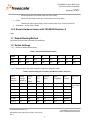
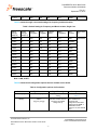
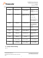
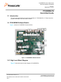
P1025RDB-PA Quick Start Quide Document Number: 926-26826 Rev. 0.1 September 16, 2011 o Power/reset button are located at the rear of the casing o Power LED and Ethernet LED are located at the front of the casing Power o Internal open frame power supply, which converts 220V AC to 12V DC and 5V DC. Schematics – OrCad; PCB - Allegro 1.2.3 Known Hardware Issues with 700-26826 Revision A None. 1.3 Default Booting Method By default, the boot loader executes from NOR flash. 1.4 Switch Settings Table 1 shows the default switch setting. Table 1: Board Default Switch Setting Switch 1 2 3 4 5 6 7 8 SW4 ON ON OFF OFF OFF OFF ON ON SW3 OFF ON OFF ON OFF ON ON ON Table 2 shows the dual core switch settings for frequency and boot location. Table 2: Switch Setting for Frequency and Boot Location, dual Core Switch Settings SW4[1:6] Switch Settings SW3[2:3] Core0 Freq Core1 Freq Platform (MHz) DDR Freq(MHz) Boot Location Boot Holdoff (MHz) (MHz) 11 0000 10 533 533 267 667 NOR 533 533 267 667 SD/MMC Core0 boot; Core1 holdoff 11 0001 10 11 0010 10 533 533 267 667 SPI 11 0011 10 533 533 267 667 NAND 11 0100 10 400 400 267 667 NOR 11 0101 10 400 400 267 667 SD/MMC 11 0110 10 400 400 267 667 SPI Freescale Semiconductor, Inc P1025RDB-PA Quick Start Guide © 2011 Freescale Semiconductors 6501 William Cannon Drive West, Austin, Texas 78735 U.S.A -4-