1
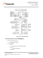
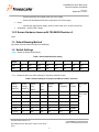
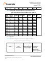
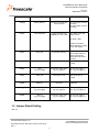
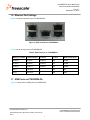
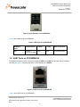
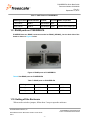
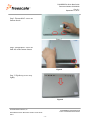
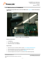
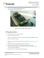
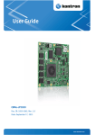
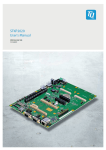
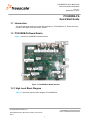
P1025RDB-PA Quick Start Quide Document Number: 926-26826 Rev. 0.1 September 16, 2011 P1025RDB-PA Quick Start Guide 1.1 Introduction This quick start guide applies to boards with assembly rev "700-26826 Rev A". Please check the top side of the board to see the revision number. 1.2 P1025RDB-PA Board Details Figure 1 shows the P1025RDB-PA board interface. Figure 1: P1025RDB-PA Board Interface 1.2.1 High Level Block Diagram Figure 2 shows the high level block diagram of P1025RDB-PA. Freescale Semiconductor, Inc P1025RDB-PA Quick Start Guide © 2011 Freescale Semiconductors 6501 William Cannon Drive West, Austin, Texas 78735 U.S.A -1- P1025RDB-PA Quick Start Quide Document Number: 926-26826 Rev. 0.1 September 16, 2011 Figure 2: High Level Block Diagram 1.2.2 Key Features of the P1025RDB-PA Freescale QorIQ architecture CPU o QorIQ P1025E, 533 MHz Memory Sub-system o SDRAM o NOR Flash o The 1Gbyte (8 bit x 4 chip) DDR3 SDRAM 16MB 16 bit NOR Flash NAND Flash: Freescale Semiconductor, Inc P1025RDB-PA Quick Start Guide © 2011 Freescale Semiconductors 6501 William Cannon Drive West, Austin, Texas 78735 U.S.A -2- P1025RDB-PA Quick Start Quide Document Number: 926-26826 Rev. 0.1 September 16, 2011 o 256 Kbit M24256 I2C EEPROM o 128 Mbit SPI flash o I2C Board 128x8 bit memory o SD/MMC connector to interface with the SD memory card PCI-E o PCI-E lane 0: mini-PCI-E X1 connector with USB 2.0 signal o PCI-E lane 1: One PCI-E X1 connector USB 2.0 o o eTSEC1: Connected to RGMII PHY –AR8021 o eTSEC2: Connected to SGMII PHY –VSC8221 o eTSEC3: Connected to RGMII PHY –AR8021 UART o X4 PMC connectors to support QE TDM function with T1/E1 daughtcard and SLIC card. o UEC1: Connect to MII PHY –KSZ8041NL o UEC5: Connect to RMII PHY –KSZ8041NL o Full duplex serial RS-485 port MISC LED Power LED (Green) Link LED (Green) on each RJ45 ethernet connector Activities LED (Yellow) on each RJ45 ethernet connector o JTAG/COP for debugging o Reset: Manual Reset and software reset function will be used on the design o I2C Serial EEPROM – Board identification (System ID and DDR SPD) Real-time clock POR (Power On Reset Configurations) o DUART interface: supports two UARTs up to 115200 bps for console display; Dual RJ45 slot are used for these 2 UART ports. QUICC Engine o Dual Type A USB slot, connected to USB PHY via USB HUB Ethernet o 32MB SLC NAND Flash Supports critical POR setting changed via switches on board PCB Freescale Semiconductor, Inc P1025RDB-PA Quick Start Guide © 2011 Freescale Semiconductors 6501 William Cannon Drive West, Austin, Texas 78735 U.S.A -3- P1025RDB-PA Quick Start Quide Document Number: 926-26826 Rev. 0.1 September 16, 2011 o Power/reset button are located at the rear of the casing o Power LED and Ethernet LED are located at the front of the casing Power o Internal open frame power supply, which converts 220V AC to 12V DC and 5V DC. Schematics – OrCad; PCB - Allegro 1.2.3 Known Hardware Issues with 700-26826 Revision A None. 1.3 Default Booting Method By default, the boot loader executes from NOR flash. 1.4 Switch Settings Table 1 shows the default switch setting. Table 1: Board Default Switch Setting Switch 1 2 3 4 5 6 7 8 SW4 ON ON OFF OFF OFF OFF ON ON SW3 OFF ON OFF ON OFF ON ON ON Table 2 shows the dual core switch settings for frequency and boot location. Table 2: Switch Setting for Frequency and Boot Location, dual Core Switch Settings SW4[1:6] Switch Settings SW3[2:3] Core0 Freq Core1 Freq Platform (MHz) DDR Freq(MHz) Boot Location Boot Holdoff (MHz) (MHz) 11 0000 10 533 533 267 667 NOR 533 533 267 667 SD/MMC Core0 boot; Core1 holdoff 11 0001 10 11 0010 10 533 533 267 667 SPI 11 0011 10 533 533 267 667 NAND 11 0100 10 400 400 267 667 NOR 11 0101 10 400 400 267 667 SD/MMC 11 0110 10 400 400 267 667 SPI Freescale Semiconductor, Inc P1025RDB-PA Quick Start Guide © 2011 Freescale Semiconductors 6501 William Cannon Drive West, Austin, Texas 78735 U.S.A -4- P1025RDB-PA Quick Start Quide Document Number: 926-26826 Rev. 0.1 September 16, 2011 11 0111 10 400 400 267 667 NAND Table 3 shows the single core switch settings for frequency and boot location. Table 3: Switch Setting for Frequency and Boot Location, Single Core Switch Settings SW4[1:6] Switch Settings SW3[2:3] Core0 Freq(MHz ) Core1 Freq(MHz ) Platform (MHz) DDR Freq(MHz) Boot Location Boot Holdoff 110000 01 533 N/A 267 667 NOR Core0 boot 110001 01 533 N/A 267 667 SD/MMC 110010 01 533 N/A 267 667 SPI 110011 01 533 N/A 267 667 NAND 110100 01 400 N/A 267 667 NOR 110101 01 400 N/A 267 667 SD/MMC 110110 01 400 N/A 267 667 SPI 110111 01 400 N/A 267 667 NAND 100000 01 667 N/A 333 667 NOR 100001 01 667 N/A 333 667 SD/MMC 100010 01 667 N/A 333 667 SPI 100011 01 667 N/A 333 667 NAND Note: 1=ON; 0=OFF; Table 4 shows the all configuration options that are available on the board. Table 4: Configuration options of all switches Switch Signal name Signal Meaning Setting SW4[1:6] SWITCH[1:6] Frequency and boot ROM setting For more details, refer to Table 2 SW4[7] LGPL5 (cfg_boot_seq[1]) Indicates whether the boot sequencer is enabled during boot-up OFF: Enables boot sequencer and configuration information loaded from I2C ROM. A valid ROM must be present. If not, the card will hang. Freescale Semiconductor, Inc P1025RDB-PA Quick Start Guide © 2011 Freescale Semiconductors 6501 William Cannon Drive West, Austin, Texas 78735 U.S.A -5- P1025RDB-PA Quick Start Quide Document Number: 926-26826 Rev. 0.1 September 16, 2011 ON: Disables boot sequer SW4[8] FBANK_SELECT Indicates which NOR flash bank is selected OFF: Uses upper 4 sectors for booting ON: Uses middle 4 sectors for booting SW3[1] CFG_SDWIDTH Configs the width of the SD/MMC bus, 4-bit or 8-bit OFF: Width = 4bits, SPI interface active ON: Width = 8bits Software can read the status of this bit by reading the I2C 8-bit register. SW3[2] TEST_SEL Personality selection SW3[3] DMA1_DACK_N Freescale use only SW3[4] LA19 (cfg_host_agt[2]) Controls the setting of the cfg_host_agt[2] pin SW3[5] USB1_STP Freescale use only SW3[6] SWITCH7 Reserved SW3[7] LA18 (cfg_host_agt[1]) Controls the setting of the cfg_host_agt[1] pin ON: cfg_host_agt[1] = 1 OFF: cfg_host_agt[1] = 0 SW3[8] LWE1_N (cfg_host_agt[0]) Controls the setting of the cfg_host_agt[0] pin ON: cfg_host_agt[0] = 1 OFF: cfg_host_agt[0] = 0 OFF: Single e500 Core Device (P1016) ON: Dual e500 Core Device (P1025) Must be set OFF for P1025E ON: cfg_host_agt[2] = 1 OFF: cfg_host_agt[2] = 0 Must be set OFF for P1025E Default ON 1.5 Jumper Default Setting J20: 2-3 Freescale Semiconductor, Inc P1025RDB-PA Quick Start Guide © 2011 Freescale Semiconductors 6501 William Cannon Drive West, Austin, Texas 78735 U.S.A -6- P1025RDB-PA Quick Start Quide Document Number: 926-26826 Rev. 0.1 September 16, 2011 1.6 Ethernet Port Settings Figure 3 shows the ethernet ports on P1025RDB-PA. Figure 3: Ethernet Ports on P1025RDB-PA Table 5 lists all ethernet ports on P1025RDB-PA. Table 5: Ethernet ports on P1025RDB-PA Marking on board P1025 Interface In uboot In Linux Mode of operation eTSEC1 eTSEC1 eTSEC1 eth0 RGMII eTSEC2 eTSEC2 eTSEC2 eth1 SGMII eTSEC3 eTSEC3 eTSEC3 eth2 RGMII UEC1 QE UEC1 / eth3 MII UEC5 QE UEC5 / eth4 RMII 1.7 USB Ports on P1025RDB-PA Figure 4 shows the two USB ports on P1025RDB-PA. Freescale Semiconductor, Inc P1025RDB-PA Quick Start Guide © 2011 Freescale Semiconductors 6501 William Cannon Drive West, Austin, Texas 78735 U.S.A -7- P1025RDB-PA Quick Start Quide Document Number: 926-26826 Rev. 0.1 September 16, 2011 Figure 4: Dual USB Ports on P1025RDB-PA Table 6 lists USB ports on P1025RDB-PA. Table 6: USB Ports on P1025RDB-PA Marking on board P1025 Interface In uboot In Linux Mode of operation USB external PHY(ULPI)+HUB USB1 USB1 ULPI(external PHY) 1.8 UART Ports on P1025RDB-PA P1025RDB-PA has two UART connectors marked as UART0 and UART1 on the back side of the board as shown in Figure 5 below.By default the control display port is UART0. Figure 5: UART Ports on P1025RDB-PA Table 7 lists UART ports on P1025RDB-PA. Freescale Semiconductor, Inc P1025RDB-PA Quick Start Guide © 2011 Freescale Semiconductors 6501 William Cannon Drive West, Austin, Texas 78735 U.S.A -8- P1025RDB-PA Quick Start Quide Document Number: 926-26826 Rev. 0.1 September 16, 2011 Table 7: UART Ports on P1025RDB-PA Marking on board P1025 Interface In uboot In Linux TOP UART1 UART1 eserial1/ttyS1 ttyS1 BOT UART0 UART0 eserial0/ttyS0 ttyS0 Mode of operation Default control display port 1.9 RS485 ports on P1025RDB-PA P1025RDB have two RS485 connectors marked as RS485_1&RS485_2 on the back side of the board as shown in Figure 6 below. Figure 6: RS485 ports on P1025RDB-PA Table 8 lists RS485 ports on P1025RDB-PA Table 7: RS485 ports on P1025RDB-PA Marking on board P1025 Interface In uboot In Linux RS485_1 QE UEC7 / ttyQE0 RS485_2 QE UEC3 / ttyQE1 1.10 Getting off the Enclosure When set the switch or jumpers, follow these 3 steps to open the enclosure: Freescale Semiconductor, Inc P1025RDB-PA Quick Start Guide © 2011 Freescale Semiconductors 6501 William Cannon Drive West, Austin, Texas 78735 U.S.A -9- P1025RDB-PA Quick Start Quide Document Number: 926-26826 Rev. 0.1 September 16, 2011 Step1: Disassemble 2 screws on bottom chassis Figure 7 Step2: Disassemble 2 screws on both side of the bottom chassis Figure 8 Step 3: Slip the top cover away lightly Figure 9 Freescale Semiconductor, Inc P1025RDB-PA Quick Start Guide © 2011 Freescale Semiconductors 6501 William Cannon Drive West, Austin, Texas 78735 U.S.A - 10 - P1025RDB-PA Quick Start Quide Document Number: 926-26826 Rev. 0.1 September 16, 2011 1.11 TDM Function on P1025RDB-PA P1025RDB-PA support PMC card to achieve QE TDM function. Figure 10 shows connection for TDM function. Figure 10: PMC card on P1025RDB-PA Hardware requirements: P1025RDB-PA; FSL T1/E1 PMC card: PQ-MDS-T1 Zarlink SLIC module: Le71HR8820G Prepare steps: Get off the top cover of enclosure. Refer to section 1.10 Getting off the Enclosure Get off the board from the enclosure by disassembly all of 4pcs stews on board. Insert T1/E1 PMC card and Voice card. Refer to Figure 11 Insert two telephone lines into two RJ11 connectors of SLIC module respectively. Freescale Semiconductor, Inc P1025RDB-PA Quick Start Guide © 2011 Freescale Semiconductors 6501 William Cannon Drive West, Austin, Texas 78735 U.S.A - 11 - P1025RDB-PA Quick Start Quide Document Number: 926-26826 Rev. 0.1 September 16, 2011 Power on the board and run the software which can support TDM. Refer to QUICC ENGINE TDM User Manual for more software operation steps. Pick up the telephones and speak each other. Figure 11 Insert T1/E1 PMC card and Voice card 1.12 Preparing the Board 1. Ensure that board is not connected to the power. 2. Ensure that the power switch is OFF. NOTE: It is recommended to wear a wrist strap while preparing the P1025RDB-PA board to get protection from electrical charges. 3. Set switches and jumper header settings, as mentioned in the Table 1: Board Default Switch Setting. 4. Plug the power cable into the receptacle on the back of the chassis. 5. Attach an RS-232 cable between the P1025RDB-PA UART0 port and a host PC. 6. Open a serial console emulator on your PC, such as TeraTerm or HyperTerminal, in order to communicating with P1025RDB-PA. 7. Configure the host PC’s serial port with the following settings: Freescale Semiconductor, Inc P1025RDB-PA Quick Start Guide © 2011 Freescale Semiconductors 6501 William Cannon Drive West, Austin, Texas 78735 U.S.A - 12 - P1025RDB-PA Quick Start Quide Document Number: 926-26826 Rev. 0.1 September 16, 2011 Data rate: 115200 bps Number of data bits: 8 Parity: None Number of Stop bits: 1 Flow Control: Hardware/None 8. Switch ON the power button given on the back of the chassis. The board should boot and show the u-boot console messages. An example u-boot log is given in Section 1.12.1 Example U-boot log. 9. A mini Root File System (mini.rootfs.ext2.gz.uboot) with limited application are preloaded in the Nor flash. However a larger Root File System (max.rootfs.ext2.gz.uboot) offered both in USB stick and BSP DVD are recommended to use, refer to the User_Manual_QorIQ_SDK_20110709.doc document for bring up. 1.12.1 Example U-boot log U-Boot 2010.12-00063-g8669298-dirty (Jul 09 2011 - 14:37:56) CPU0: P1025E, Version: 1.1, (0x80ec0311) Core: E500, Version: 5.1, (0x80212051) Clock Configuration: CPU0:533.333 MHz, CPU1:533.333 MHz, CCB:266.667 MHz, DDR:333.333 MHz (666.667 MT/s data rate) (Asynchronous), LBC:16.667 MHz QE:266.667 MHz L1: D-cache 32 kB enabled I-cache 32 kB enabled Board: P1025RDB CPLD: V2.6 PCBA: V2.0 rom_loc: nor lower bank SD/MMC : 4-bit Mode eSPI : Enabled I2C: ready SPI: ready DRAM: Detected UDIMM(s) DDR: 1 GiB (DDR3, 32-bit, CL=5, ECC off) FLASH: 16 MiB Freescale Semiconductor, Inc P1025RDB-PA Quick Start Guide © 2011 Freescale Semiconductors 6501 William Cannon Drive West, Austin, Texas 78735 U.S.A - 13 - P1025RDB-PA Quick Start Quide Document Number: 926-26826 Rev. 0.1 September 16, 2011 L2: 256 KB enabled NAND: 32 MiB MMC: FSL_ESDHC: 0 Firmware 'Microcode version 0.0.1 for P1021 r1.0' for 1021 V1.0 QE: uploading microcode 'Microcode for P1021 r1.0' version 0.0.1 PCIe1: Root Complex of mini PCIe SLOT, no link, regs @ 0xffe0a000 PCIe1: Bus 00 - 00 PCIe2: Root Complex of PCIe SLOT, no link, regs @ 0xffe09000 PCIe2: Bus 01 - 01 Video: No radeon video card found! In: serial Out: serial Err: serial Net: eTSEC2 is in sgmii mode. eTSEC1, eTSEC2, eTSEC3 Hit any key to stop autoboot: 0 =>NOTE: Linux login: root, Password: root 1.13 CAUTION Aviod touching any area of open frame power circuitry inside the chassis. High Voltage in the power circuitry can prove fatal and hazardous. Avoid touching areas of integrated circuitry and connectors; static discharge can damage circuits. Freescale Semiconductor, Inc P1025RDB-PA Quick Start Guide © 2011 Freescale Semiconductors 6501 William Cannon Drive West, Austin, Texas 78735 U.S.A - 14 - P1025RDB-PA Quick Start Quide Document Number: 926-26826 Rev. 0.1 September 16, 2011 How to Reach Us: Home Page: www.freescale.com E-mail: [email protected] USA/Europe or Locations Not Listed: Freescale Semiconductor Technical Information Center, CH370 1300 N. Alma School Road Chandler, Arizona 85224 +1-800-521-6274 or +1-480-7682130 [email protected] Europe, Middle East, and Africa: Freescale Halbleiter Deutschland GmbH Technical Information Center Schatzbogen 7 81829 Muenchen, Germany +44 1296 380 456 (English) +46 8 52200080 (English) +49 89 92103 559 (German) +33 1 69 35 48 48 (French) [email protected] Japan: Freescale Semiconductor Japan Ltd. Headquarters ARCO Tower 15F 1-8-1, Shimo-Meguro, Meguro-ku, Tokyo 153-0064, Japan 0120 191014 or +81 3 5437 9125 [email protected] Asia/Pacific: Freescale Semiconductor Hong Kong Ltd. Technical Information Center 2 Dai King Street Tai Po Industrial Estate Tai Po, N.T., Hong Kong +800 2666 8080 [email protected] For Literature Requests Only: Freescale Semiconductor Literature Distribution Center P.O. Box 5405 Denver, Colorado 80217 1-800-521-6274 or 303-675-2140 Fax: 303-675-2150 LDCForFreescaleSemiconductor@hibbert group.com Information in this document is provided solely to enable system and software implementers to use Freescale Semiconductor products. There are no express or implied copyright licenses granted hereunder to design or fabricate any integrated circuits or integrated circuits based on the information in this document. Freescale Semiconductor reserves the right to make changes without further notice to any products herein. Freescale Semiconductor makes no warranty, representation or guarantee regarding the suitability of its products for any particular purpose, nor does Freescale Semiconductor assume any liability arising out of the application or use of any product or circuit, and specifically disclaims any and all liability, including without limitation consequential or incidental damages. “Typical” parameters that may be provided in Freescale Semiconductor data sheets and/or specifications can and do vary in different applications and actual performance may vary over time. All operating parameters, including “Typicals”, must be validated for each customer application by customer’s technical experts. Freescale Semiconductor does not convey any license under its patent rights nor the rights of others. Freescale Semiconductor products are not designed, intended, or authorized for use as components in systems intended for surgical implant into the body, or other applications intended to support or sustain life, or for any other application in which the failure of the Freescale Semiconductor product could create a situation where personal injury or death may occur. Should Buyer purchase or use Freescale Semiconductor products for any such unintended or unauthorized application, Buyer shall indemnify and hold Freescale Semiconductor and its officers, employees, subsidiaries, affiliates, and distributors harmless against all claims, costs, damages, and expenses, and reasonable attorney fees arising out of, directly or indirectly, any claim of personal injury or death associated with such unintended or unauthorized use, even if such claim alleges that Freescale Semiconductor was negligent regarding the design or manufacture of the part. Freescale and the Freescale logo are trademarks of Freescale Semiconductor, Inc. Reg. U.S. Pat. & Tm. Off. All other product or service names are the property of their respective owners. © 2011 Freescale Semiconductor, Inc. All rights reserved. P1025RDB-PA QSG Document number: 926-26826 16 September 2011 Freescale Semiconductor, Inc P1025RDB-PA Quick Start Guide © 2011 Freescale Semiconductors 6501 William Cannon Drive West, Austin, Texas 78735 U.S.A - 15 -