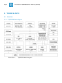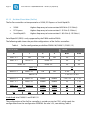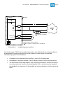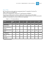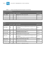
1
TQMP2020
User's Manual
TQMP2020 UM 102
24.05.2012
User's Manual l TQMP2020 UM 102 l © 2012, by TQ-Group
Page i
Table of contents
1.
1.1
1.2
1.3
1.4
1.5
1.6
1.7
1.8
1.9
1.10
2.
3.
3.1
3.1.1
3.1.2
3.2
3.2.1
3.2.1.1
3.2.1.2
3.2.1.3
3.2.2
3.2.2.1
3.2.2.2
3.2.2.3
3.2.2.4
3.2.2.5
3.2.2.6
3.2.2.7
3.2.2.8
3.2.2.9
3.2.2.10
3.2.3
3.2.3.1
3.2.3.2
3.2.3.3
3.2.3.4
3.2.3.5
3.2.3.6
ABOUT THIS MANUAL...................................................................................................................... 1
Copyright............................................................................................................................................. 1
Tips on safety...................................................................................................................................... 1
Symbols and typographic conventions ..................................................................................... 1
Handling and ESD tips ..................................................................................................................... 2
Registered trademarks..................................................................................................................... 2
Imprint .................................................................................................................................................. 3
Disclaimer ............................................................................................................................................ 3
Copyright and licence expenses................................................................................................... 3
Further applicable documents / presumed knowledge ....................................................... 4
Acronyms and definitions............................................................................................................... 5
BRIEF DESCRIPTION .......................................................................................................................... 7
TECHNICAL DATA.............................................................................................................................. 8
Overview .............................................................................................................................................. 8
TQMP2020 block diagram .............................................................................................................. 8
System components......................................................................................................................... 9
Electronics .........................................................................................................................................10
CPU ......................................................................................................................................................10
Parallel Modes of the Enhanced Three Speed Ethernet Controller (eTSEC)..................10
Serializer/Deserializer (SerDes) ...................................................................................................12
USB.......................................................................................................................................................13
Reset logic and supervisor............................................................................................................13
Supervision 3.3 V .............................................................................................................................13
Supervision 2.5 V .............................................................................................................................14
Supervision 1.8 V .............................................................................................................................14
Supervision 1.5 V .............................................................................................................................14
Supervision VDD..............................................................................................................................14
Supervision VREF.............................................................................................................................14
Supervision VTT ...............................................................................................................................14
Reset LED ...........................................................................................................................................14
Self-reset ............................................................................................................................................15
JTAG reset TRST# .............................................................................................................................16
CPU configuration...........................................................................................................................17
Reset configuration of the hardware ........................................................................................17
Freely available reset configuration ..........................................................................................26
Other configuration signals .........................................................................................................26
Configuration data in the EEPROM............................................................................................27
Error handling and default configuration................................................................................28
Settings via the boot sequencer.................................................................................................29
Page ii
User's Manual l TQMP2020 UM 102 l © 2012, by TQ-Group
Table of contents (continued)
3.2.4
3.2.4.1
3.2.4.2
3.2.4.3
3.2.4.4
3.2.4.5
3.2.4.6
3.2.4.7
3.2.4.8
3.2.4.9
3.2.4.10
3.2.4.11
3.2.5
3.2.6
3.2.7
3.2.8
3.2.8.1
3.2.8.2
3.2.8.3
3.2.8.4
3.2.9
3.3
3.3.1
3.3.2
3.3.2.1
3.3.2.2
3.3.2.3
3.3.2.4
3.3.2.5
3.3.3
3.3.3.1
3.3.3.2
3.3.3.3
Clock....................................................................................................................................................30
Internal clock structure of the P2020/2010 .............................................................................30
Internal clock structure of the P1020/1011 and P1021/1012 ............................................31
System clock SYSCLK......................................................................................................................32
Core-Complex-Bus clock CCB_CLK ............................................................................................32
Processor Core clock CORE_CLK.................................................................................................32
Local Bus clock LCLK.......................................................................................................................32
Memory bus clocks: DDRCLK, DDR_CLK, MCKx, MCK#........................................................34
Real time clock RTC.........................................................................................................................34
USB clock USB_CLK.........................................................................................................................34
SERDES clock SD_REF_CLK/SD_REF_CLK# ..............................................................................34
Standard clock frequencies..........................................................................................................35
Local Bus ............................................................................................................................................35
NOR flash............................................................................................................................................36
DDR3 SDRAM....................................................................................................................................36
I2C bus .................................................................................................................................................37
Data EEPROM....................................................................................................................................38
Configuration EEPROM..................................................................................................................38
RTC (real time clock) .......................................................................................................................39
Temperature supervision..............................................................................................................39
General-Purpose-I/O ......................................................................................................................39
Supply .................................................................................................................................................40
Power sequencing ..........................................................................................................................40
Supply inputs....................................................................................................................................41
VCC3V3IN / main supply ...............................................................................................................41
VBAT / RTC supply...........................................................................................................................41
LVDD / Ethernet-I/O supply..........................................................................................................41
BVDD / Local Bus supply ...............................................................................................................41
CVDD / supply USB, SDHC and SPI.............................................................................................42
Supply outputs.................................................................................................................................42
VCC3V3OUT ......................................................................................................................................42
VCC2V5OUT ......................................................................................................................................42
VCC1V8OUT ......................................................................................................................................42
User's Manual l TQMP2020 UM 102 l © 2012, by TQ-Group
Page iii
Table of contents (continued)
3.4
3.4.1
3.4.2
3.4.3
3.4.3.1
3.4.3.2
3.5
3.5.1
3.5.2
3.6
3.6.1
3.6.2
3.6.3
3.7
4.
4.1
4.2
5.
5.1
5.2
5.3
6.
6.1
Interfaces to other systems and devices ..................................................................................42
Serial interfaces................................................................................................................................42
COP/JTAG interface ........................................................................................................................43
External bus / other interfaces ....................................................................................................44
Treatment of unused pins ............................................................................................................44
Pinout according to functional groups ....................................................................................44
Cooling ...............................................................................................................................................58
Power dissipation............................................................................................................................58
Heat sink.............................................................................................................................................58
Mechanics..........................................................................................................................................58
General information .......................................................................................................................58
Notes of treatment..........................................................................................................................59
Dimensions........................................................................................................................................59
Boot loader........................................................................................................................................60
SAFETY REQUIREMENTS AND PROTECTIVE REGULATIONS ................................................61
EMC......................................................................................................................................................61
ESD.......................................................................................................................................................61
CLIMATIC AND OPERATIONAL CONDITIONS ..........................................................................62
Reliability and service life..............................................................................................................62
Environment protection................................................................................................................63
RoHS compliance ............................................................................................................................63
APPENDIX ..........................................................................................................................................64
References .........................................................................................................................................64
Page iv
User's Manual l TQMP2020 UM 102 l © 2012, by TQ-Group
Table directory
Table 1:
Table 2:
Table 3:
Table 4:
Table 5:
Table 6:
Table 7:
Table 8:
Table 9:
Table 10:
Table 11:
Table 12:
Table 13:
Table 14:
Table 15:
Table 16:
Table 17:
Table 18:
Table 19:
Table 20:
Terms and conventions............................................................................................................. 1
Acronyms....................................................................................................................................... 5
eTSEC configuration possibilities P2020/10 (P1020/11, P1021/12)...........................11
SerDes configuration possibilities P2020/10 (P1020/11, P1021/12) .........................12
Reset options..............................................................................................................................16
Legend for Table 7, Table 8 and Table 9 ............................................................................17
Reset configuration ..................................................................................................................18
Free reset configuration (general purpose) ......................................................................26
Static configuration signals....................................................................................................26
Configuration data in EEPROM .............................................................................................27
Standard clock frequencies (with P2020) ..........................................................................35
Assignment chip selects at the Local Bus ..........................................................................35
IIC1 device addresses...............................................................................................................37
Requirements for 3.3 V external ...........................................................................................41
Requirements for VBAT ...........................................................................................................41
Signals COP/JTAG interface ...................................................................................................43
Pinout according to functional groups ..............................................................................45
Stack heights, overview...........................................................................................................59
Stack heights, detailed ............................................................................................................60
Further applicable documents..............................................................................................64
User's Manual l TQMP2020 UM 102 l © 2012, by TQ-Group
Page v
Illustration directory
Illustration 1:
Illustration 2:
Illustration 3:
Illustration 4:
Illustration 5:
Illustration 6:
Illustration 7:
Illustration 8:
Illustration 9:
TQMP2020 block diagram................................................................................................. 8
Feedback HRESET_REQ#..................................................................................................15
Wiring of TRST# ..................................................................................................................16
P2020/2010 clock subsystem, block diagram...........................................................30
P1020/1011 and P1021/1012 clock subsystem, block diagram ..........................31
Length alignment Local Bus...........................................................................................33
Supply structure (simplified) ..........................................................................................40
Stack heights (not to scale).............................................................................................59
Overall dimensions (top view through board) .........................................................60
Page vi
User's Manual l TQMP2020 UM 102 l © 2012, by TQ-Group
Revision history
Rev. Date
Name
100
Petz
07.07.2011
Pos.
3.2.3
Table 7
101
03.01.2012
Petz
102
24.05.2012
Petz
3.2.3.6
3.2.4.6
Illustration 6
3.2.4.6
Table 17
3.2.3.2
3.7
Modification
Document created
CPU configuration legend updated
”Meaning P2020” for values “10” and “11” of
signals PORDEVSR[20:21] corrected
Warning added
“100 MHz” for TQMP1xxx removed
Added
Explanation for Illustration 6 added
Type of signal HRESET# specified more precisely
Typo
Link to Wiki added
User's Manual l TQMP2020 UM 102 l © 2012, by TQ-Group
Page 1
1. ABOUT THIS MANUAL
1.1 Copyright
Copyright protected © 2012 by TQ-Components GmbH.
This User’s Manual may not be copied, reproduced, translated, changed or distributed,
completely or partially in electronic, machine readable, or in any other form without the written
consent of TQ-Components GmbH.
1.2 Tips on safety
Improper or incorrect handling of the product can substantially reduce its life span.
1.3 Symbols and typographic conventions
Table 1:
Terms and conventions
Symbol / Visual Cue
Meaning
This symbol represents the handling of electrostatic-sensitive
modules and / or components. These components are often
damaged / destroyed by the transmission of a voltage higher than
about 50 V. A human body usually only experiences electrostatic
discharges above approximately 3,000 V.
This symbol indicates the possible use of voltages higher than 24 V.
Please note the relevant statutory regulations in this regard. Noncompliance with these regulations can lead to serious damage to
your health and cause damage / destruction of the component.
This symbol indicates a possible source of danger. Acting against the
procedure described can lead to possible damage to your health
and / or cause damage / destruction of the material used.
This symbol represents important details or aspects for working with
TQ-products.
Command
This specification is used to state the complete file name with its
corresponding extension.
Page 2
User's Manual l TQMP2020 UM 102 l © 2012, by TQ-Group
1.4 Handling and ESD tips
General handling of your TQ-products
The TQ-product may only be used and serviced by certified personnel
who have taken note of the information, the safety regulations in this
document and all related rules and regulations.
A general rule is: do not touch the TQ-product during operation. This
is especially important when switching on, changing jumper settings
or connecting other devices without ensuring beforehand that the
power supply of the system has been switched off.
Violation of this guideline may result in damage / destruction of the
module and be dangerous to your health.
Improper handling of your TQ-product would render the guarantee
invalid.
Proper ESD handling
The electronic components of your TQ-product are sensitive to
electrostatic discharge (ESD).
Always wear antistatic clothing, use ESD-safe tools, packing materials
etc., and operate your TQ-product in an ESD-safe environment.
Especially when you switch modules on, change jumper settings, or
connect other devices.
1.5 Registered trademarks
TQ-Components GmbH aims to adhere to the copyrights of all the used graphics and texts in all
publications and strives to use original or licence-free graphics and texts.
All the brand names and trademarks mentioned in the publication, including those protected by
a third party, unless specified otherwise in writing, are subjected to the specifications of the
current copyright laws and the proprietary laws of the present registered proprietor without any
limitation. One should conclude that brands and trademarks are protected through the rights of
a third party.
User's Manual l TQMP2020 UM 102 l © 2012, by TQ-Group
Page 3
1.6 Imprint
TQ-Components GmbH
Gut Delling, Mühlstraße 2
82229 Seefeld
Tel:
+49 (0) 8153 9308–0
Fax:
+49 (0) 8153 9308–134
Email: [email protected]
Web:
http://www.tq-group.com/
1.7 Disclaimer
TQ-Components GmbH does not guarantee that the information in this manual is up-to-date,
correct, complete or of good quality. Nor does TQ-Components GmbH assume guarantee for
further usage of the information. Liability claims against TQ-Components GmbH, referring to
material or non-material related damages, caused due to usage or non-usage of the information
given in the manual, or caused due to usage of erroneous or incomplete information, are
exempted, as long as there is no proven, intentional or negligent fault of TQ-Components GmbH.
TQ-Components GmbH explicitly reserves the rights to change or add to the contents of this
manual or parts of it without special notification.
1.8 Copyright and licence expenses
The drivers and utilities for the used components as well as the BIOS are subject to the
copyrights of the respective manufacturers. The licence conditions of the respective
manufacturer are to be adhered to.
Boot loader licence expenses are paid by TQ-Components GmbH and are included in the price.
Licence expenses for the operating system and applications are not taken into consideration and
must be separately calculated / declared.
Page 4
User's Manual l TQMP2020 UM 102 l © 2012, by TQ-Group
1.9 Further applicable documents / presumed knowledge
•
Specifications and manual of the used modules:
These documents describe the service, functionality and special characteristics of the
used module (incl. BIOS).
•
Specifications of the used components:
The manufacturer’s specifications of the used components, for example CompactFlash
cards, are to be taken note of. They contain, if applicable, additional information that
must be taken note of for safe and reliable operation. These documents are stored at
TQ-Components GmbH.
•
Chip errata:
It is the user’s responsibility to make sure all errata published by the manufacturer of
each component are taken note of. The manufacturer’s advice should be followed.
•
Software behaviour:
No warranty can be given, nor responsibility taken for any unexpected software
behaviour due to deficient components.
•
General expertise:
Expertise in electrical engineering / computer engineering is required for the
installation and the use of the device.
User's Manual l TQMP2020 UM 102 l © 2012, by TQ-Group
1.10 Acronyms and definitions
Table 2:
Acronym
BGA
Acronyms
Description
Ball Grid Array
COP
Common On-chip Processor
CPLD
Complex Programmable Logic Device
CPU
Central Processing Unit
CRC
Cyclic Redundancy Check
DDR
Double Data Rate
DMA
Direct Memory Access
ECC
Error Checking and Correction
EEPROM
Electrically Erasable Programmable Read-only Memory
EMC
Electromagnetic Compatibility
ESD
Electrostatic Discharge
FR-4
Flame Retardant 4
GMII
Gigabit Media Independent Interface
GP
General Purpose
IP
Ingress Protection
I2C
Inter-Integrated Circuit
JTAG
Joint Test Action Group
LED
Light Emitting Diode
LSB
Least Significant Bit
LVTTL
Low Voltage Transistor Transistor Logic
MII
Media-Independent Interface
MSB
Most Significant Bit
NAND
Not-and
NC
Not Connected
NOR
Not-or
PHY
Physical (Interface)
Page 5
Page 6
User's Manual l TQMP2020 UM 102 l © 2012, by TQ-Group
Table 2:
Acronym
Acronyms (continued)
Description
PLL
Phase Locked Loop
POR
Power-On Reset
RGMII
Reduced Gigabit Media Independent Interface
RMII
Reduced Media Independent Interface
ROM
Read-Only Memory
RTBI
Reduced Ten-Bit Interface
RTC
Real-Time Clock
RoHS
Restriction of (the use of certain) Hazardous Substances
SDHC
Secure Digital High Capacity
SDRAM
Synchronous Dynamic Random Access Memory
SGMII
Serial Gigabit Media Independent Interface
SMD
Surface-Mounted Device
SPI
Serial Peripheral Interface
SerDes
Serializer/Deserializer
TBI
Ten-Bit Interface
TSEC
Three-Speed Ethernet Controller
UART
Universal Asynchronous Receiver/Transmitter
ULPI
UTMI+ Low Pin count Interface
UPM
User Programmable Machine
USB
Universal Serial Bus
User's Manual l TQMP2020 UM 102 l © 2012, by TQ-Group
Page 7
2. BRIEF DESCRIPTION
The TQMP2020 is a universal Minimodule based on the Freescale QorIQ processor P2020.
It extends the range of Power-Architecture based modules towards High-End, with reduced size.
The computing performance of the P2020 (dual core CPU) is approximately double of the
MPC8548, at significantly lower power dissipation. Alternatively, a P2010 (single core) can be
assembled on the module. In this case, the computing performance corresponds to the
MPC8548. The power dissipation is reduced further.
A P1020, or P1021 (dual core), or a P1011, or P1012 (single core) can be assembled on the same
printed circuit board as an alternative.
The characteristic features of the module are:
•
Dual or Single Core, max. 1.2 GHz
•
DDR3, 32 or 64 bit with ECC
•
4 × SERDES, configurable as PCI Express, SGMII or Serial Rapid/IO
•
3 × Gbit-Ethernet
The Starterkit STKP2020 is used as an Eval-Board for the TQMP2020.
All function relevant pins of the CPU are routed to the module plug connectors.
Even when using the module, the user has complete freedom, as in a design-in solution.
Page 8
User's Manual l TQMP2020 UM 102 l © 2012, by TQ-Group
3. TECHNICAL DATA
3.1 Overview
3.1.1 TQMP2020 block diagram
Illustration 1:
TQMP2020 block diagram
User's Manual l TQMP2020 UM 102 l © 2012, by TQ-Group
3.1.2 System components
•
QorIQ processor P2020 or P2010, optional P1020/11 and P1021/12
•
Oscillator for CPU clocks
•
Reset generator and power fail logic
•
CPLD for reset configuration
•
Voltage regulator for 2.5 V, 1.8 V, 1.5 V, core voltage VDD, VTT, VREF
•
Switch for 3.3 V
•
DDR3 SDRAM
•
NOR Flash
•
Serial EEPROM (data + configuration)
•
RTC
•
Temperature sensors
•
RS232 driver for two serial interfaces
•
Board-to-board plug connector system
Page 9
Page 10
User's Manual l TQMP2020 UM 102 l © 2012, by TQ-Group
3.2 Electronics
3.2.1 CPU
As an alternative to the P2020, (dual core) a P2010 (single core) can be assembled on the same
module. Unless otherwise noted, the name P2020 also stands for the P2010 in the following, and
equally for derivatives with and without encryption.
The P2020 offers a large number of interfaces. On account of the high data rates special attention
is to be paid to the interfaces mentioned in the following.
3.2.1.1 Parallel Modes of the Enhanced Three Speed Ethernet Controller (eTSEC)
The three gigabit Ethernet interfaces TQMP2020 are implemented via eTSECs. All relevant pins
are routed to the module plug connectors, to enable the user to use all possible interface modes
supported by the CPU. PHY and transformer have to be integrated on the baseboard for RFtechnical reasons.
•
MII mode
− Highest frequency to be transmitted: 25 MHz (Tx- and Rx clock 100 Mbit/s)
•
RMII mode
− Highest frequency to be transmitted: 50 MHz (Tx- and Rx clock @ 100 Mbit/s)
− Lower number of signals than with MII
− Timing is tighter than with MII, because both clock edges are used
•
GMII-and TBI mode
− Highest frequency to be transmitted: 125 MHz (Tx- and Rx clock @ 1 Gbit/s)
− Transmit clock changes signal of GTX_CLK to TX_CLK as well as direction with
fallback to 10/100 Mbit/s (MII)
•
RGMII-and RTBI mode
− Highest frequency to be transmitted: 125 MHz (Tx- and Rx clock @ 1 Gbit/s)
− Lower number of signals than with (G)MII or TBI
− Timing tighter than with (G)MII and TBI, because both clock edges are used
− Source clocking
User's Manual l TQMP2020 UM 102 l © 2012, by TQ-Group
Page 11
The configuration of the interface modes is carried out via the CPLD, which reads the
configuration from the configuration EEPROM. See also 3.2.3.
The above-described interfaces, except RGMII, are supported by the P2020 as well as P2010.
With all other CPUs, (P1020/11 as well as P1021/12) only two eTSECs (eTSEC1 / 3) can be
operated in the parallel mode with RGMII. The following table shows the possible eTSECconfigurations.
Table 3:
eTSEC configuration possibilities P2020/10 (P1020/11, P1021/12)
eTSEC1
eTSEC2
Standard interface
Inactive
Reduced interface
Inactive
Inactive
Reduced interface
Inactive
Standard interface
SGMII
Inactive
Reduced interface
SGMII
Inactive
SGMII
Inactive
Reduced interface
SGMII
Inactive
eTSEC3
SGMII
Inactive
SGMII
Inactive
SGMII
Inactive
Reduced interface
SGMII
Inactive
Underlined: also P1020/11 and P1021/12
Standard interfaces:
Reduced interfaces:
GMII, TBI, MII
RGMII, RTBI, RMII
If the parallel mode is used the IO voltages at the CPU (= LVDD) and at the
PHYs must be the same. See also 3.3.2.3.
Page 12
User's Manual l TQMP2020 UM 102 l © 2012, by TQ-Group
3.2.1.2 Serializer/Deserializer (SerDes)
The SerDes controller can be operated as a SGMII, PCI Express or Serial Rapid/IO:
•
SGMII
Highest frequency to be transmitted: 625 MHz (1.25 Gbit/s)
•
PCI Express
Highest frequency to be transmitted: 1.25 GHz (2.5 Gbit/s)
•
Serial Rapid/IO
Highest frequency to be transmitted: 1.563 GHz (3.125 Gbit/s)
Serial Rapid/IO (SRIO) is only supported by the P2020 and the P2010.
The following table shows the possible configurations of the SerDes controllers.
Table 4:
SerDes configuration possibilities P2020/10 (P1020/11, P1021/12)
SerDes lanes
Gbaud
0
1
2
3
0&1
2&3
PEX1: × 1
Off
Off
Off
2.5
–
PEX1: × 1
PEX2: × 1
PEX3: × 2
2.5
2.5
PEX3: × 2
2.5
2.5
PEX1: × 2
PEX1: × 4
SRIO2: × 1
SRIO1: × 1
2.5
Off
Off
SRIO2: × 4
3.125
–
1.25 / 2.5 / 3.125
SRIO2: × 1
SRIO1: × 1
SGMII2
SGMII3
1.25 / 2.5
1.25
PEX1: × 1
SRIO1: × 1
SGMII2
SGMII3
2.5
1.25
PEX1: × 1
PEX2: × 1
SGMII2
SGMII3
2.5
1.25
SGMII2
SGMII3
2.5
1.25
Off
Off
–
–
PEX1: × 2
Off
Off
Underlined: also P1020/11 and P1021/12
The configuration of the SerDes controller is carried out via the CPLD, which reads the
configuration from the configuration EEPROM. See also 3.2.3, considering Table 3.
User's Manual l TQMP2020 UM 102 l © 2012, by TQ-Group
Page 13
3.2.1.3 USB
In contrast to P2020/10 and the P1021/12, the P1020/11 possesses two USB controllers.
Because Local Bus and USB2 are multiplexed with the P1020/11, the second USB-PHY (ULPI) must
be connected at the Local Bus. This means that the second USB-PHY is almost completely limited
in its function, or the NOR flash can only be partly used.
3.2.2 Reset logic and supervisor
The reset logic contains the following functions:
•
Supervision of the following voltages used on module:
− 3.3 V, 2.5 V, 1.8 V, 1.5 V
− VDD (core voltage)
− VREF (reference voltage for DDR3 SDRAM)
− VTT (termination voltage for DDR3 SDRAM)
•
External reset input (debounced with 200 ms delay)
•
PGOOD output (e.g., for power sequencing of an external PHY)
•
Indication of the reset state by a LED (HRESET# low
LED lights up)
3.2.2.1 Supervision 3.3 V
Tolerance range of the fed supply voltage:
VCC3V3ID = 3.201 V to 3.465 V = 3.3 V −3% / +5%
Permitted voltage range for CPU and 3.3 V logic:
VCC3V3 = 3.135 V to 3.465 V
Tolerance of the voltage supervision, voltage drop in VCC3V3 taken into account:
VReset = 3.135 V to 3.201 V
Page 14
User's Manual l TQMP2020 UM 102 l © 2012, by TQ-Group
3.2.2.2 Supervision 2.5 V
This supply voltage is generated and monitored internally.
3.2.2.3 Supervision 1.8 V
This supply voltage is generated and monitored internally.
3.2.2.4 Supervision 1.5 V
This supply voltage is generated and monitored internally.
3.2.2.5 Supervision VDD
The required core voltage depends on the CPU (P2 or P1). It is set at the voltage regulator by
component placement, and in the supervisor by the configuration.
The user cannot change this setting.
3.2.2.6 Supervision VREF
The DDR3 reference voltage VREF is monitored internally.
3.2.2.7 Supervision VTT
The DDR3 termination voltage VTT is generated and monitored internally.
3.2.2.8 Reset LED
•
LED is controlled via the HRESET#-Signal; HRESET# low
•
The supervisor provides duration for at least 200 ms of the HRESET# pulse.
The reset is thereby visible even if the reset pulse at RESIN# is very short.
LED lights up
User's Manual l TQMP2020 UM 102 l © 2012, by TQ-Group
Page 15
3.2.2.9 Self-reset
The P2020 can request a hardware reset by software. The signal HRESET_REQ# signals the reset
requirement. It can be triggered by software by writing to register bit RSTCR[HRESET_REQ].
The following participants can also trigger HRESET_REQ#:
•
Boot sequencer error (Preamble, CRC)
•
eSDHC boot loader error (e.g., boot signature)
•
eSPI boot loader error (e.g., boot signature)
•
Not correctable eLBC ECC Error during boot phase of NAND flash
•
Rapid/IO
•
e500 watchdog
RESIN# is connected to HRESET_REQ# with a resistor on the module (Illustration 2).
Illustration 2:
Feedback HRESET_REQ#
This enables a self-reset trigger. The self-reset can be prevented, or be linked to other conditions
depending on the external wiring on the baseboard (see Table 5).
Page 16
User's Manual l TQMP2020 UM 102 l © 2012, by TQ-Group
The following table shows the reset options, depending on the wiring of the RESIN#-Signals.
Table 5:
Reset options
External wiring at RESIN# input
Reset function
None
Self-reset is possible
(HRESET_REQ# is switched through to RESIN# on the module)
Pull-up ≤ 2k2 to VCC3V3
No self-reset possible
(HRESET_REQ# cannot trigger a reset on the module)
Open-Drain-/Open Collector output or
push button to DGND
Self-reset is possible
In addition, an external reset can be triggered by applying a low
level at RESIN#
Push-Pull output or Open-Drain-/Open
Collector output with pull-up ≤ 2k2 to
VCC3V3
No self-reset, but only external reset possible
(HRESET_REQ# cannot trigger a reset on the module)
3.2.2.10 JTAG reset TRST#
TRST# will be pulled low by HRESET#, it can still however be triggered separately (COP/JTAGDebugging). This is achieved with the following circuit on the module.
RESOUT# from
Supervisor
Illustration 3:
Wiring of TRST#
User's Manual l TQMP2020 UM 102 l © 2012, by TQ-Group
Page 17
3.2.3 CPU configuration
Table 6:
Legend for Table 7, Table 8 and Table 9
Binary value in bold
"Default" (Freescale)
internal value if nothing is connected (internal pull-up)
Binary value greyed out
"Reserved"
Light green highlighted
Value is fixed in the design (not alterable)
Dark green highlighted
Value is set in the design by comparators (not by CPLD / EEPROM)
Blue highlighted
Default values of CPLD
do not use
3.2.3.1 Reset configuration of the hardware
The signals listed in Table 7 (column 2) are used to define the reset configuration of the CPU on
the module.
Page 18
User's Manual l TQMP2020 UM 102 l © 2012, by TQ-Group
Table 7:
Reset configuration
Config signal
IO signal at the P2020
Register
cfg_boot_seq[0:1]
LGPL3/LFWP#,
LGPL5
PORBMSR[10:11]
cfg_sys_pll[0:2]
LA[29:31]
PORPLLSR[26:30]
Value
Meaning P2020
00
Reserved
Reserved
01
Boot sequencer is enabled on I2C1
with normal I2C addressing mode.
Boot sequencer is enabled on I2C1
with normal I2C addressing mode.
10
Boot sequencer is enabled on I2C1
with extended I2C addressing mode.
Boot sequencer is enabled on I2C1
with extended I2C addressing mode.
11
Boot sequencer is disabled.
No I²C ROM is accessed.
Boot sequencer is disabled.
No I²C ROM is accessed.
000
4:1
4:1
001
5:1
5:1
010
6:1
6:1
011
8:1
Reserved
Reserved
Reserved
000
4:1
Reserved
001
9:2 (4.5:1)
Reserved
010
1:1
1:1
011
3:2 (1.5:1)
3:2 (1.5:1)
100
2:1
2:1
101
5:2 (2.5:1)
5:2 (2.5:1)
110
3:1
3:1
111
7:2 (3.5:1)
Reserved
others
cfg_core0_pll[0:2]
LBCTL,
LALE,
LGPL2/LOE#/LFRE#
PORPLLSR[10:15]
Meaning P1020 / P1021
User's Manual l TQMP2020 UM 102 l © 2012, by TQ-Group
Table 7:
Config signal
cfg_core1_pll[0:2]
Reset configuration (continued)
IO signal at the P2020
Register
LWE0#,
PORPLLSR[2:7]
UART_SOUT1,
READY_P1
cfg_ddr_pll[0:2]
cfg_srds_pll_toe
cfg_plat_speed
Page 19
TSEC_1588_CLK_OUT,
TSEC_1588_PULSE_OUT[1:2]
TRIG_OUT/READY_P0
LA23
PORPLLSR[18:22]
PORDEVSR2[10]
PORDEVSR2[14]
Value
Meaning P2020
Meaning P1020 / P1021
000
4:1
Reserved
001
9:2 (4.5:1)
Reserved
010
1:1
1:1
011
3:2 (1.5:1)
3:2 (1.5:1)
100
2:1
2:1
101
5:2 (2.5:1)
5:2 (2.5:1)
110
3:1
3:1
111
7:2 (3.5:1)
Reserved
000
Reserved
3:1
001
4:1
4:1
010
6:1
6:1
011
8:1
8:1
100
10:1
10:1
101
12:1
Reserved
110
Reserved
Reserved
111
Synchronous mode
Synchronous mode
0
Enable PLL lock time-out counter,
POR-sequence waits for SerDes PLL
to lock while time-out counter has
not expired
Not used
1
Disable PLL lock time-out counter,
POR-sequence waits for SerDes
PLL to lock
Not used
0
Platform clock <333 MHz
Platform clock <300 MHz and >267 MHz
1
Platform clock ≥333 MHz
Platform clock ≥300 MHz
Page 20
User's Manual l TQMP2020 UM 102 l © 2012, by TQ-Group
Table 7:
Reset configuration (continued)
Config signal
IO signal at the P2020
Register
cfg_core0_speed
LA24
PORDEVSR2[12]
cfg_core1_speed
LA25
PORDEVSR2[13]
cfg_ddr_speed
LA26
PORDEVSR2[15]
cfg_sys_speed
LA28
PORDEVSR2[21]
cfg_cpu[0:1]_boot
LA27,
LA16
PORBMSR[0:1]
Value
Meaning P2020
Meaning P1020 / P1021
Core 0 clock ≤450 MHz
0
Core 0 clock ≤1 GHz
1
Core 0 clock >1 GHz
Core 0 clock >450 MHz
0
Core 1 clock ≤1 GHz
Core 1 clock ≤450 MHz
1
Core 1 clock >1 GHz
Core 1 clock >450 MHz
0
DDR clock <500 MHz
DDR clock <450 MHz
1
DDR clock ≥500 MHz
DDR clock ≥450 MHz
0
System clock <66 MHz
Reserved
System clock ≥66 MHz
System clock ≥66 MHz
00
1
CPU boot holdoff mode for both
cores. The e500 cores are prevented
from booting until configured by an
external master.
CPU boot holdoff mode for both cores. The
e500 cores are prevented from booting until
configured by an external master.
01
e500 core 1 is allowed to boot
without waiting for configuration by
an external master, while e500 core 0
is prevented from booting until
configured by an external master or
the other core.
e500 core 1 is allowed to boot without
waiting for configuration by an external
master, while e500 core 0 is prevented from
booting until configured by an external
master or the other core.
10
e500 core 0 is allowed to boot
without waiting for configuration by
an external master, while e500 core 1
is prevented from booting until
configured by an external master or
the other core.
e500 core 0 is allowed to boot without
waiting for configuration by an external
master, while e500 core 1 is prevented from
booting until configured by an external
master or the other core.
11
Both e500 cores are allowed to boot
without waiting for configuration by
an external master.
Both e500 cores are allowed to boot
without waiting for configuration by an
external master.
User's Manual l TQMP2020 UM 102 l © 2012, by TQ-Group
Table 7:
Reset configuration (continued)
Config signal
IO signal at the P2020
Register
cfg_ddr_debug
DMA2_DDONE0#
PORDBGMSR[7]
cfg_device_ID[7:5]
TSEC2_TXD[4:2]
PORDEVSR[29:31]
cfg_dram_type
TSEC2_TXD1
PORDEVSR[25]
cfg_elbc_ecc
cfg_eng_use[0:7]
Page 21
MSRCID0
LA[20:22],
UART_SOUT0,
TRIG_OUT/READY_P0,
MSRCID1,
MSRCID4,
DMA1_DDONE#
PORDEVSR[15]
PORDEVSR2
Value
0
1
xxx-----
Meaning P2020
Meaning P1020 / P1021
ECC pins driven Debug info
instead of normal ECC I/O.
(disconnect memory devices)
ECC pins driven Debug info instead of
normal ECC I/O.
(disconnect memory devices)
ECC pins in normal mode
Not used
0
ECC pins in normal mode
Device ID LSBs for Rapid/IO
hosts
DDR2 1.8 V, CKE low @ reset
1
DDR3 1.5 V, CKE low @ reset
DDR3 1.5 V, CKE low @ reset
0
eLBC ECC checking disabled
eLBC ECC checking disabled
1
000x0000
eLBC ECC checking enabled
Reserved for engineering use
eLBC ECC checking enabled
Not used
DDR2 1.8 V, CKE low @ reset
...
Reserved for engineering use
Not used
111x1110
Reserved for engineering use
Not used
111x111
1
Default
(see cfg_srds_pll_toe)
Not used
Page 22
User's Manual l TQMP2020 UM 102 l © 2012, by TQ-Group
Table 7:
Reset configuration (continued)
Config signal
IO signal at the P2020
Register
cfg_host_agt[0:2]
LWE1#/LBS1,
LA[18:19]
PORBMSR[13:15]
Value
Meaning P2020
Meaning P1020 / P1021
000
Agent on all PCIe and SRIO
Agent on all PCIe
001
Agent on PCIe 1 or host SRIO 2,
Host on PCIe 2 / SRIO 1,
Host on PCIe 3
Agent on PCIe 1,
Host on PCIe 2
010
Host on PCIe 1 or agent SRIO 2,
Agent on PCIe 2 / SRIO 1,
Host on PCIe 3
Host on PCIe 1,
Agent on PCIe 2
011
Host on PCIe 1 / SRIO 2,
Host on PCIe 2 / SRIO 1,
Agent on PCIe 3
Agent on PCIe 1 / SRIO 2,
Agent on PCIe 2 / SRIO 1,
Host on PCIe 3
Reserved
101
Agent on PCIe 1 or host SRIO 2,
Host on PCIe 2 / SRIO 1,
Agent on PCIe 3
Reserved
110
Host on PCIe 1 or agent SRIO 2,
Agent on PCIe 2 / SRIO 1,
Agent on PCIe 3
Reserved
111
Host processor / root complex
for all PCIe / SRIO
Host processor /
root complex for all PCIe
100
Reserved
User's Manual l TQMP2020 UM 102 l © 2012, by TQ-Group
Table 7:
Reset configuration (continued)
Config signal
IO signal at the P2020
Register
cfg_io_ports[0:3]
TSEC1_TXD[3:1],
TSEC2_TX_ER
PORDEVSR[9:12]
Value
Meaning P2020
0000
0001
0010
0011
0100
0101
0110
0111
1000
1001
1010
1011
1100
1101
1110
1111
PCIe 1 (x1) (2.5 Gbps) → SerDes lane 0,
SerDes lanes 1-3 powered down
SerDes lanes 0-3 powered down
PCIe 1 (x1) (2.5 Gbps) → SerDes lane 0,
PCIe 2 (x1) (2.5 Gbps) → SerDes lane 1,
PCIe 3 (x2) (2.5 Gbps) → SerDes lane 2-3
Reserved
PCIe 1 (x2) (2.5 Gbps) → SerDes lane 0-1,
PCIe 3 (x2) (2.5 Gbps) → SerDes lane 2-3
Reserved
PCIe 1 (x4) (2.5 Gbps) → SerDes lane 0-3
SRIO 2 (1x) (3.125 Gbps) → SerDes lane 0,
SRIO 1 (1x) (3.125 Gbps) → SerDes lane 1,
SerDes lanes 2-3 powered down
SRIO 2 (4x) (1.25 Gbps) → SerDes lane 0-3
SRIO 2 (4x) (2.5 Gbps) → SerDes lane 0-3
SRIO 2 (4x) (3.125 Gbps) → SerDes lane 0-3
SRIO 2 (1x) (1.25 Gbps) → SerDes lane 0,
SRIO 1 (1x) (1.25 Gbps) → SerDes lane 1,
SGMII 2 (x1) (1.25 Gbps) → SerDes lane 2,
SGMII 3 (x1) (1.25 Gbps) → SerDes lane 3
SRIO 2 (1x) (2.5 Gbps) → SerDes lane 0,
SRIO 1 (1x) (2.5 Gbps) → SerDes lane 1,
SGMII 2 (x1) (1.25 Gbps) → SerDes lane 2,
SGMII 3 (x1) (1.25 Gbps) → SerDes lane 3
PCIe 1 (x1) (2.5 Gbps) → SerDes lane 0,
SRIO 1 (1x) (2.5 Gbps) → SerDes lane 1,
SGMII 2 (x1) (1.25 Gbps) → SerDes lane 2,
SGMII 3 (x1) (1.25 Gbps) → SerDes lane 3
PCIe 1 (x1) (2.5 Gbps) → SerDes lane 0,
PCIe 2 (x1) (2.5 Gbps) → SerDes lane 1,
SGMII 2 (x1) (1.25 Gbps) → SerDes lane 2,
SGMII 3 (x1) (1.25 Gbps) → SerDes lane 3
PCIe 1 (x2) (2.5 Gbps) → SerDes lane 0-1
SGMII 2 (x1) (1.25 Gbps) → SerDes lane 2
SGMII 3 (x1) (1.25 Gbps) → SerDes lane 3
Meaning P1020 / P1021
PCIe 1 (x1) (2.5 Gbps) → SerDes lane 0,
SerDes lanes 1-3 powered down
SerDes lanes 0-3 powered down
Reserved
Reserved
Reserved
Reserved
PCIe 1 (x4) (2.5 Gbps) → SerDes lane 0-3
Reserved
Reserved
Reserved
Reserved
Reserved
Reserved
Reserved
PCIe 1 (x1) (2.5 Gbps) → SerDes lane 0,
PCIe 2 (x1) (2.5 Gbps) → SerDes lane 1,
SGMII 2 (x1) (1.25 Gbps) → SerDes lane 2,
SGMII 3 (x1) (1.25 Gbps) → SerDes lane 3
PCIe 1 (x2) (2.5 Gbps) → SerDes lane 0-1,
SGMII 2 (x1) (1.25 Gbps) → SerDes lane 2,
SGMII 3 (x1) (1.25 Gbps) → SerDes lane 3
Page 23
Page 24
User's Manual l TQMP2020 UM 102 l © 2012, by TQ-Group
Table 7:
Reset configuration (continued)
Config signal
IO signal at the P2020
Register
cfg_mem_debug
DMA2_DACK0#
PORDBGMSR[5]
Value
0
1
cfg_rio_sys_size
LGPL0/LFCLE
PORDEVSR[28]
0
1
cfg_rom_loc[0:3]
TSEC1_TXD[6:4],
TSEC1_TX_ER
PORBMSR[4:7]
0000
0001
0010
0011
0100
0101
0110
0111
1000
1001
1010
1011
1100
1101
1110
1111
cfg_sgmii2
LGPL1/LFALE
PORDEVSR[3]
0
cfg_sgmii3
TSEC_1588_ALARM_OUT2
PORDEVSR[4]
1
0
1
Meaning P2020
Meaning P1020 / P1021
Debug info from eLBC is driven on
MSRCID and MDVAL
Debug info from DDR is driven on
MSRCID and MDVAL
Large system size
(up to 65536 devices)
Small system size
(up to 256 devices)
PCIe 1
PCIe 2
SRIO 1
SRIO 2
DDR
PCIe 3
On-Chip boot ROM - SPI config
On-Chip boot ROM - eSDHC config
eLBC FCM - 8-bit NAND small page
Reserved
eLBC FCM - 8-bit NAND large page
Reserved
Reserved
eLBC GPCM - 8-bit ROM
eLBC GPCM - 16-bit ROM
eLBC GPCM - 16-bit ROM
(formerly probably GPCM - 32-bit)
eTSEC2 (SGMII) → SGMII SerDes lane
2 pins
eTSEC2 (Std.) → TSEC2_* pins
eTSEC3 (SGMII) → SGMII SerDes lane
3 pins
eTSEC3 (Std.) → TSEC3_* pins
Debug info from eLBC is driven on
MSRCID and MDVAL
Debug info from DDR is driven on
MSRCID and MDVAL
Not used
Not used
PCIe 1
PCIe 2
Reserved
Reserved
DDR
Reserved
On-Chip boot ROM - SPI config
On-Chip boot ROM - eSDHC config
eLBC FCM - 8-bit NAND small page
Reserved
eLBC FCM - 8-bit NAND large page
Reserved
Reserved
eLBC GPCM - 8-bit ROM
eLBC GPCM - 16-bit ROM
eLBC GPCM - 16-bit ROM
(formerly probably GPCM - 32-bit)
Not used
Not used
eTSEC3 → SGMII
eTSEC3 → RGMII
User's Manual l TQMP2020 UM 102 l © 2012, by TQ-Group
Table 7:
Reset configuration (continued)
Config signal
IO signal at the P2020
Register
cfg_srds_refclk
TSEC_1588_ALARM_OUT1
PORDEVSR2[18]
cfg_tsec_reduce
EC_MDC
PORDEVSR[0]
Value
0
1
0
1
cfg_tsec1_prtcl[0:1]
TSEC1_TXD0,
TSEC1_TXD7
PORDEVSR[6:7]
cfg_tsec2_prtcl[0:1]
TSEC2_TXD0,
TSEC2_TXD7
PORDEVSR[18:19]
00
01
10
11
00
01
10
11
cfg_tsec3_prtcl[0:1]
UART_RTS[0:1]#
PORDEVSR[20:21]
00
01
10
11
cfg_sdhc_cd_pol_sel
TSEC2_TXD5/TSEC3_TX_EN
PORDEVSR[23]
0
1
Meaning P2020
Meaning P1020 / P1021
SerDes Ref Clock = 125 MHz
SerDes Ref Clock = 100 MHz
eTSEC1 & eTSEC2 in reduced pin
mode (RTBI, RGMII, RMII)
eTSEC1 & eTSEC2 in std. width
(TBI, GMII, MII)
Reserved
ETSEC1 → MII / RMII
ETSEC1 → GMII / RGMII
ETSEC1 → TBI / RTBI
Reserved
ETSEC2 → MII / RMII
(if not configured to SGMII)
ETSEC2 → GMII / RGMII
(if not configured to SGMII)
eTSEC2 → TBI / RTBI
(if not configured to SGMII)
Reserved
eTSEC3 → RMII
(if not configured to SGMII)
eTSEC3 → RGMII
(if not configured to SGMII)
eTSEC3 → RTBI
(if not configured to SGMII)
eSDHC Card-detect polarity is not
inverted
eSDHC Card-detect polarity is not
inverted
SerDes Ref Clock = 125 MHz
SerDes Ref Clock = 100 MHz
eTSEC1 in reduced mode (RGMII)
Reserved
Reserved / eTSEC1 → SGMII
Reserved / eTSEC1 → SGMII
eTSEC1 → RGMII
Reserved / eTSEC1 → SGMII
Not used
Not used
Not used
Not used
Reserved / eTSEC3 → SGMII
Reserved / eTSEC3 → SGMII
eTSEC3 → RGMII
Reserved / eTSEC3 → SGMII
Not used
Not used
Page 25
Page 26
User's Manual l TQMP2020 UM 102 l © 2012, by TQ-Group
3.2.3.2 Freely available reset configuration
The signals listed in the following table are not used on the module. The baseboard can pass additional configuration data to the CPU on these
signals, if desired. These do not influence the configuration of the CPU by hardware after a reset, but can merely be utilised by software.
Table 8:
Config signal
cfg_gpinput[0:15]
Free reset configuration (general purpose)
IO-Signal at the P2020
LAD[0:15]
Register
GPPORCR[0:15]
Value
Meaning P2020
0x nnnn_0000
General-purpose POR config → not used
Meaning P1020 / P1021
General-purpose POR config → not used
3.2.3.3 Other configuration signals
The module generates the signals listed in the following table. They are not read during reset, but must be applied permanently.
Table 9:
Config signal
Static configuration signals
IO-Signal at the P2020
Register
Value
Meaning P2020
Meaning P1020 / P1021
LVDD_VSEL
LVDD_VSEL
IOVSELSR[30:31]
0
3.3 V: eTSEC[1:3], Eth. Management, 1588
3.3 V: eTSEC[1:3], Eth. Management, 1588
1
2.5 V: eTSEC[1:3], Eth. Management, 1588
2.5 V: eTSEC[1:3], Eth. Management, 1588
BVDD_VSEL[0:1]
BVDD_VSEL[0:1]
IOVSELSR[26:27]
00
3.3 V: Local Bus, GPIO[8:15]
3.3 V: Local Bus, GPIO[8:15] / CE_PB*, CE_PC0
01
2.5 V: Local Bus, GPIO[8:15]
2.5 V: Local Bus, GPIO[8:15] / CE_PB*, CE_PC0
10
1.8 V: Local Bus, GPIO[8:15]
1.8 V: Local Bus, GPIO[8:15] / CE_PB*, CE_PC0
11
3.3 V: Local Bus, GPIO[8:15]
3.3 V: Local Bus, GPIO[8:15] / CE_PB*, CE_PC0
00
3.3 V: USB, eSDHC, SPI
3.3 V: USB, eSDHC, SPI
01
2.5 V: USB, eSDHC, SPI
2.5 V: USB, eSDHC, SPI
10
1.8 V: USB, eSDHC, SPI
1.8 V: USB, eSDHC, SPI
11
3.3 V: USB, eSDHC, SPI
3.3 V: USB, eSDHC, SPI
CVDD_VSEL[0:1]
CVDD_VSEL[0:1]
IOVSELSR[22:23]
Page 27
User's Manual l TQMP2020 UM 102 l © 2012, by TQ-Group
3.2.3.4 Configuration data in the EEPROM
Table 10 shows how the configuration data is stored in the EEPROM. The single fields with
configuration data consist of an Enable bit and the actual data field in each case:
Enable
0 = Tri-State
1 = Actively driven during Reset
Table 10:
Address
0
Configuration data see Table 7
Configuration data in EEPROM
Content
Bit 7
Bit 6
Bit 5
0
0
1
Enable | cfg_boot_seq[0:1]
2
cfg_core0_pll[0:2]
3
cfg_ddr_pll[0:2]
5
6
Bit 2
Bit 1
0
1
0
1
Enable | cfg_sys_pll[0:2]
Bit 0
cfg_cpu[0:1]_boot
Enable | cfg_core1_pll[0:2]
Enable
Enable | cfg_srds_pll_toe Enable | cfg_plat_speed
Enable | cfg_ddr_debug
Enable | cfg_dram_type Enable | cfg_elbc_ecc
cfg_host_agt[2]
9
Enable | cfg_rio_sys_size
10
cfg_sgmii2
Enable | cfg_host_agt[0:1]
Enable | cfg_mem_debug
Enable | cfg_rom_loc[0:3]
Enable
Enable | cfg_sgmii3 Enable | cfg_srds_refclk Enable | cfg_tsec_reduce
cfg_tsec1_prtcl[0:1]
12
Enable | cfg_sdhc_cd_pol_sel
Enable | cfg_tsec2_prtcl[0:1]
unused
Enable
Enable | cfg_eng_use[0:2]
Enable | cfg_io_ports[0:3]
11
Enable
Enable | cfg_device_ID[7:5]
cfg_eng_use[3:7]
8
0
Enable
cfg_core0_speed Enable | cfg_core1_speed Enable | cfg_ddr_speed Enable | cfg_sys_speed
7
13
Bit 3
Fixed Configuration ID
1
4
Bit 4
unused
unused
CRC checksum
Enable
Enable | cfg_tsec3_prtcl[0:1]
unused
unused
unused
Page 28
User's Manual l TQMP2020 UM 102 l © 2012, by TQ-Group
3.2.3.5 Error handling and default configuration
The CPLD transmits a reset sequence on the I2C bus (IIC1) before the real access.
This ensures that accesses still running at the time of the reset are completed and the EEPROM is
ready to be read.
To ensure the system integrity, the configuration mechanism handles the following errors:
•
I2C protocol error
•
Configuration ID missing
•
CRC incorrect
In these cases, the CPLD starts another attempt. If this also fails, the default configuration will be
passed to the CPU (highlighted in blue in Table 7). This guarantees that the system boots, but
with certain functional limitations (lower clock, interfaces partly not available).
The CRC used the polynomial x8 + x2 + x + 1 and the start value 0xFF. A tool, which calculates the
CRC, can be made available, if required.
Tip 1
Damaged or deleted configuration data generates a CRC error and causes the use of the
default configuration. With the again bootable system, the EEPROM can be rewritten.
Another possibility is, to pull IIC1_SDA "low". This leads to a protocol error (NACK) and
therefore the default configuration to be used. In this manner a system with two different
boot configurations can be operated: e.g., a normal operation (config-EEPROM) with boot
process via PCIe or eSDHC and a service or emergency operation (default-config) with boot
loader in the NOR flash.
Tip 2
The enable-bits enable the configuration of single fields not via the module, but via the
baseboard without reprogramming the EEPROM. Thus, e.g., the field "cfg_device_ID" can be
configured with different Device-IDs depending on the baseboard. Pull-ups / pull-downs or
active drivers (driver conflicts possible) must be provided for this on the baseboard.
During the reset phase respective, power-up the corresponding signals are driven by the
CPLD. As these signals are outputs of the CPU or the module, a possible driver’s conflict
must be taken into account in the design of the baseboard. The signals UART_SOUT0#
(cfg_eng_use3), UART_SOUT1# (cfg_core1_pll1) and TSEC2_TXD5/TSEC3_TX_EN
(cfg_sdhc_cd_pol_sel) are an exception. These signals are separated from the plug
connector during the reset phase of the module to improve the system integrity.
User's Manual l TQMP2020 UM 102 l © 2012, by TQ-Group
Page 29
3.2.3.6 Settings via the boot sequencer
The CPU configuration with CPU specific boot sequencer cannot replace the configuration via
the CPU pins, but only complement. Because it runs before the software starts, it can carry out
additional settings, which cannot or should not be set by software.
The standard software delivered with the module (U-Boot) does not depend on the boot
sequencer.
The standard software (U-Boot) delivered with the module does not rely on the boot sequencer.
The configuration with the boot sequencer starts after the end of the reset. In certain cases, the
configuration via the boot sequencer is indispensable:
•
Multiprocessor environments
•
Preconfiguration to boot via other systems or interfaces
(e.g., PCIe, Rapid/IO, SDRAM...)
•
Fixing of incompatibilities with reset values
(e.g., preset functionality of the bus driver control LBCTL)
Wrong data can lead to an unbootable system!
This condition can be fixed by temporary activation of the default
configuration, because the boot sequencer is deactivated then.
See also tip 2 under 3.2.3.5.
The CPU operates the I2C bus at about 160 kHz when the boot sequencer
is used.
Devices, which can only work at a maximum of 100 kHz may not be
connected to IIC1, when the boot sequencer is enabled.
This only affects the baseboard as all I2C bus devices on the TQMP2020
can operate at 400 kHz.
Page 30
User's Manual l TQMP2020 UM 102 l © 2012, by TQ-Group
3.2.4 Clock
3.2.4.1 Internal clock structure of the P2020/2010
Illustration 4:
P2020/2010 clock subsystem, block diagram
(Source: Freescale)
User's Manual l TQMP2020 UM 102 l © 2012, by TQ-Group
3.2.4.2 Internal clock structure of the P1020/1011 and P1021/1012
Only for P1020/11
Illustration 5:
General:
Different clocks
Reduced because of
32 bit DDR
P1020/1011 and P1021/1012 clock subsystem, block diagram
(Source: Freescale)
Page 31
Page 32
User's Manual l TQMP2020 UM 102 l © 2012, by TQ-Group
3.2.4.3 System clock SYSCLK
In normal operation, SYSCLK is generated on the module.
The Platform- or Core-Complex-Bus clock (see 3.2.4.4) is generated by multiplication from this.
The Memory bus clock (see 0) can also be generated.
The frequency is 66.666 MHz.
Spread spectrum clocking is possible on request, but not standard.
3.2.4.4 Core-Complex-Bus clock CCB_CLK
The Platform- or Core-Complex-Bus clock CCB_CLK is generated from the system clock signal
SYSCLK by multiplication. The multiplication factor is fixed by the reset configuration. The signal
merely exists CPU internally. It is used for the L2 cache (internal) as well as for the Local Bus and
other interfaces.
The frequency is set to 400 MHz by default.
Core frequencies of 600, 800, 1000 and 1200 MHz are possible with it, see 3.2.4.5.
TQMP1xxx: 266 / 333 / 400 / 533 MHz = 0.5 × frequency CORE_CLK or constant 266 MHz.
3.2.4.5 Processor Core clock CORE_CLK
The core clock CORE_CLK is generated by multiplication from CCB_CLK.
The multiplication factor is fixed by the reset configuration.
The signal merely exists CPU internally and is used for the e500v2 core(s).
Possible frequencies are 600, 800, 1000 or 1200 MHz.
TQMP1020, TQMP1021: 333 to 800 MHz, gradation depending on CCB_CLK and multiplication
factors.
3.2.4.6 Local Bus clock LCLK
The Local Bus clock LCLK is generated from CCB_CLK divided by LCRR[CLKDIV] (values 4, 8 or 16).
The division factor LCRR[CLKDIV] is configurable at run time.
The signal is used for the Local Bus.
Possible frequencies with CCB_CLK = 400 MHz are 25, 50, 100 MHz.
The maximum possible frequency LCLK for the P2020 is 150 MHz.
TQMP1xxx:
•
with CCB_CLK = 400 MHz:
25, 50 MHz
•
with CCB_CLK = 267 MHz:
17, 33, 66 MHz
Page 33
User's Manual l TQMP2020 UM 102 l © 2012, by TQ-Group
CPU Module
Mainboard
CPU
LBus PLL
L
LCLK0
Local Bus
Devices
LCLKn
Zero
Delay
additional clocks, if necessary
LSYNC_OUT
L
LSYNC_IN
Routing Length on module is matched:
L(LCKL0) = L(LCKLn) = L(LSYNC_OUT) + L(LSYNC_IN)
Illustration 6:
Length alignment Local Bus
Two clock outputs LCKL[0:1] are provided externally. A zero-delay buffer has to be provided on
the baseboard, if more participants have to be supplied as clock outputs are available.
The following applies for the feedback:
•
A feedback is only required if the Local Bus is used in PLL Enable mode.
•
No feedback is required, however, if the PLL Bypass mode is used (it may be present).
•
The adjustment of the cable length is only required if participants, which use the clock
are connected to the Local Bus on the baseboard. If this is not the case, the length of
the feedback is unimportant. On the module are no bus participants, which require the
clock.
Page 34
User's Manual l TQMP2020 UM 102 l © 2012, by TQ-Group
3.2.4.7 Memory bus clocks: DDRCLK, DDR_CLK, MCKx, MCK#
The Platform clock CCB_CLK can be used as an alternative to the Memory Bus clock DDR_CLK,
or be generated by an own PLL from DDRCLK (= SYSCLK).
The frequency of the Memory Bus clock DDR_CLK corresponds to the DDR data rate.
It is twice as high as the frequency of the signals MCKx and MCK#.
Favourite frequency: DDR_CLK = 800 MHz, multiplied from DDRCLK (66.666 MHz) × 12.
TQMP1xxx: 666 MHz from DDRCLK (66.666 MHz) × 10.
3.2.4.8 Real time clock RTC
The signal RTC is a clock input, through which a time base can be created which is independent
of the system clock. The signal RTC is available at the connector but not connected on the
module.
More detailed information can be found in the hardware specification of the CPU (1).
3.2.4.9 USB clock USB_CLK
The signal USB_CLK is required for the interface to the external USB-PHY. (The USB controller
runs synchronically to CCB_CLK). If USB is used, a 60-MHz clock must be fed at this signal.
More detailed information can be found in the hardware specification of the CPU (1).
3.2.4.10 SERDES clock SD_REF_CLK/SD_REF_CLK#
The signal pair SD_REF_CLK/SD_REF_CLK# is required for the SERDES interface. (The system side
runs synchronically to CCB_CLK). If the SERDES interface is used, depending on protocol and data
rate, a clock of 100 or 125 MHz must be supplied here.
If no SERDES clock is supplied, the reset configuration has to prevent that the CPU waits for the
SERDES-PLL to lock after a reset. See also cfg_srds_pll_toe under 3.2.3.1.
More detailed information can be found in the hardware specification of the CPU (1).
User's Manual l TQMP2020 UM 102 l © 2012, by TQ-Group
Page 35
3.2.4.11 Standard clock frequencies
Table 11:
Clock
Standard clock frequencies (with P2020)
Frequency [MHz]
SYSCLK
CCB_CLK
CORE_CLK
LCLK
DDRCLK
DDR_CLK
MCKx/MCKx#
RTC
USB_CLK
SD_REF_CLK/SD
_REF_CLK#
66.666
400
1,200
25 / 50 / 100
66.666
800
400
Freely selectable
60
100 / 125
Remark
Input clock system-PLL
Platform clock
Core clock
Standard frequency underlined
Input clock DDR-PLL, frequency identical with SYSCLK
= Data rate
= half data rate = physical clock
Not connected on module
When required externally
When required externally,
frequency depending on protocol and data rate
3.2.5 Local Bus
The available chip selects are assigned as follows:
Table 12:
Assignment chip selects at the Local Bus
Chip select
Usage on TQMP2020
LCS0#/CS_NOR#
NOR flash (boot)
LCS1#
Free
LCS2#
Free
LCS3#
Free
LCS4#
Free
LCS5#/DMA2_DREQ1#
Free, if not used for DMA
LCS6#/DMA2_DACK1#
Free, if not used for DMA
LCS7#/DMA2_DDONE1#
Free, if not used for DMA
Page 36
User's Manual l TQMP2020 UM 102 l © 2012, by TQ-Group
3.2.6 NOR flash
•
3.3-V flashes Micron PC28FxxxM29EW,
alternatively EON EN29GL, 16 bit wide
•
Connected at the Local Bus
because of multiplexed addresses and data
•
One bank with 16 bit bus width
•
16 to 256 Mibyte
•
Access time 100 ns
•
Chip-select LCS0#
addresses via a latch
The status signal RY/BY# of the flash is not used by the CPU.
The event of write and erasure cycles must be monitored by polling.
3.2.7 DDR3 SDRAM
•
DDR3 SDRAMs, 64 bit wide, alternatively with / without ECC
P10xx: 32 bit wide, with / without ECC
•
512 Mibyte to 1 Gibyte (2 Gibyte announced)
P10xx: 256 to 512 Mibyte (1 Gibyte announced)
•
DDR3-800 (400 MHz clock)
P10xx: DDR3-667 (333 MHz clock)
•
Chip select MCS0#, with stacked DDR also MCS1#
•
BGA package, 96 balls
Page 37
User's Manual l TQMP2020 UM 102 l © 2012, by TQ-Group
3.2.8 I2C bus
All I2C bus devices on the module are connected to the I2C controller IIC1 of the CPU.
Table 13 shows the used addresses.
All devices are designed for a maximum I2C clock frequency of 400 kHz.
The pull-ups available on the module are sufficient for the bus loads on the module.
If required that more devices are connected to the bus, additional pull-ups must be connected in
parallel on the baseboard, to achieve sufficient low-high edges.
Table 13:
IIC1 device addresses
Device
Data EEPROM
Configuration
EEPROM SE97B (*)
Configuration
EEPROM SE97B Write
Protect (*)
Temperature Sensor
SE97B (*)
Temperature Sensor
SA560004EDP
Real Time Clock
DS1337
Power Manager
ADM1068
(*)
Combined in one device
MSB
LSB
1
1
0
0
1
1
0
0
0 (A2)
1 (A2)
0 (A1)
1 (A1)
0 (A0)
1 (A0)
R/W
R/W
0
1
1
0
1 (A2)
1 (A1)
1 (A0)
R/W
0
0
1
1
1 (A2)
1 (A1)
1 (A0)
R/W
1
0
0
1
1
0
0
R/W
1
1
0
1
0
0
0
R/W
1
0
0
0
1
0 (A1)
0 (A0)
R/W
Page 38
User's Manual l TQMP2020 UM 102 l © 2012, by TQ-Group
3.2.8.1 Data EEPROM
The serial EEPROM can store, e.g., characteristics of the module and customer specific parameter
data. In the EEPROM single memory cells can be deleted and be overwritten in contrast to flash.
At delivery the EEPROM is erased. It can, e.g. save application parameters permanently.
•
32 Kibyte = 256 Kibit or not assembled
•
Is freely available for user’s data
•
Can be used for boot sequencer when required
•
Controlled via I2C controller IIC1, device address see Table 13
3.2.8.2 Configuration EEPROM
At delivery the configuration-EEPROM contains a standard reset configuration (see 3.2.3.5).
•
Combined device SE97B
•
256 bytes = 2 Kibit
•
Used for reset configuration
•
Update by the CPU is possible
•
Temporary or permanent write protection possible
•
Controlled via I2C controller IIC1, device address see Table 13
An altered reset configuration can lead under certain circumstances to
an unbootable system. In this case there are several possibilities to get
back to a functioning reset configuration:
•
It is possible to connect an external master (programming unit) at the I2C bus.
The support of TQ-Components can recommend a suitable tool.
•
Recovery by module software: It is a prerequisite that the software in the NOR flash on
the module runs with the default reset configuration, and that the I2C bus can be
accessed.
For a “how to” see 3.2.3.5, tip 1.
User's Manual l TQMP2020 UM 102 l © 2012, by TQ-Group
Page 39
3.2.8.3 RTC (real time clock)
As the CPU does not contain an internal bufferable RTC, it was connected externally.
•
RTC DS1337U, controlled via I2C bus of the CPU
•
Battery buffering possible (battery on baseboard at VBAT)
•
Alarm outputs INTA# and SQW/INTB# (Open Drain) are routed to a common pin
•
Controlled via I2C controller IIC1, device address see Table 13
•
30 ppm oscillator tolerance over the whole temperature range
3.2.8.4 Temperature supervision
•
Control of all sensors via I2C controller IIC1, device addresses see Table 13
•
Measuring point 1: chip temperature of the CPU by internal measuring diode
P10xx: availability of the internal diode unclear
Implemented by remote channel SA560004EDP
•
Measuring point 1a (assembly option):
External sensor alternatively to CPU internal measuring diode, implemented by remote
channel SA560004EDP on top side between CPU and switching regulator
•
Measuring point 2: PCB bottom side close to DDR3
Implemented by local channel SA560004EDP
•
Measuring point 3: PCB top side between DDR3 devices
Implemented by combined device SE97B
3.2.9 General-Purpose-I/O
•
16 GPIOs, 9 of it multiplexed with other interface signals
P1020 16 GPIOs; P1021 no GPIOs
•
Configured as input after power-on reset
•
Open drain capable
•
Interrupt capable
Page 40
User's Manual l TQMP2020 UM 102 l © 2012, by TQ-Group
3.3 Supply
3.3.1 Power sequencing
The module is supplied with 3.3 V only. All other voltages are generated on the module.
The integrated power manager ensures valid power sequencing.
For that reason the external supplied 3.3 V are routed via a switch.
To guarantee the correct power sequencing for the variable I/O voltages LVDD and CVDD as well,
LVDD and CVDD may not be supplied by an external supply voltage. LVDD and CVDD must be
fed via the provided pins VCC3V3OUT, VCC2V5OUT or VCC1V8OUT (see Illustration 7).
TQMP2020
VCC3V3IN
Power Manager
OV
opt.
State Machine
VCC3V3
VCC3V3OUT
LVDD
VCC2V5
VCC2V5OUT
CVDD
VCC1V8
VCC1V8OUT
VCC1V5
VCC1V5
VREF
Range
opt.
VREF
VTT
Range
opt.
VTT
VDD
VDD
Timer
RESIN#
Illustration 7:
HRESET#
Supply structure (simplified)
User's Manual l TQMP2020 UM 102 l © 2012, by TQ-Group
Page 41
3.3.2 Supply inputs
For the supply voltages to be fed the following limits apply:
3.3.2.1 VCC3V3IN / main supply
Table 14:
VCC3V3IN
Ripple max.
Current
consumption
Requirements for 3.3 V external
3.201 V to 3.465 V
(3.3 V –3 % / +5 %)
30 mV
5A
Determined by voltage range of components and
supervisor threshold (see 3.2.2.1)
Peak to peak
TQMP2020 @ 400 / 1200 / 800 MHz (CCB / Core / DDR3)
3.3.2.2 VBAT / RTC supply
•
Supply of the RTC
•
Current consumption only, if VBAT >VCC3V3
(Connection via Schottky diode to VCC3V3 is present on module.)
Table 15:
Requirements for VBAT
Voltage VBAT 1.8 V to 5.5 V
Determined by voltage range of RTC (see 3.2.8.3)
Ripple max.
Timekeeping
current
Peak to peak
VCC3V3IN = 0 V, Oscillator running
1%
2 µA
3.3.2.3 LVDD / Ethernet-I/O supply
LVDD is generated by feedback of the voltages VCC3V3OUT or VCC2V5OUT, which are
monitored and generated on the module. In this way the necessary specifications are observed
automatically.
The driver’s configuration LVDD_VSEL is done on the module automatically, based on the
supplied voltage, see 3.2.3.3.
3.3.2.4 BVDD / Local Bus supply
BVDD always operates at 3.3 V. BVDD cannot be changed and is not accessible externally.
The driver’s configuration BVDD_VSEL[0:1] is done on the module, see 3.2.3.3.
Page 42
User's Manual l TQMP2020 UM 102 l © 2012, by TQ-Group
3.3.2.5 CVDD / supply USB, SDHC and SPI
CVDD is generated by feedback of the voltages VCC3V3OUT, VCC2V5OUT or VCC1V8OUT, which
are monitored and generated on the module. In this way the necessary specifications are
observed automatically.
The driver’s configuration CVDD_VSEL[0:1] is done on the module automatically, based on the
supplied voltage, see 3.2.3.3.
3.3.3 Supply outputs
3.3.3.1 VCC3V3OUT
VCC3V3OUT exclusively supplies the variable I/O voltages LVDD or CVDD.
An additional load is not permitted.
Voltage: 3.3 V
3.3.3.2 VCC2V5OUT
VCC2V5OUT exclusively supplies the variable I/O voltages LVDD or CVDD.
An additional load is not permitted.
Voltage: 2.5 V
3.3.3.3 VCC1V8OUT
VCC1V8OUT exclusively supplies the variable I/O voltage CVDD.
An additional load is not permitted.
Voltage: 1.8 V
3.4 Interfaces to other systems and devices
3.4.1 Serial interfaces
•
Two internal UARTs: UART1 and UART2
•
Max. 115,200 baud (limited by driver / level shifter)
•
Transceiver for TxD and RxD with RS232compatible levels
•
Additionally all signals are also available unbuffered at the module plug connectors
•
Default assembly: driver for 2 × RxD and 2 × TxD;
the control signals RTS and CTS are only available unbuffered
User's Manual l TQMP2020 UM 102 l © 2012, by TQ-Group
Page 43
3.4.2 COP/JTAG interface
All signals of the Freescale COP/JTAG interfaces (debugging interface) are made available
externally. The COP/JTAG interface encloses the following signals.
(Signal direction seen from the module or Starterkit):
Table 16:
Pin*
1
2
3
4
5
6
7
8
9
10
11
12
13
14
15
16
Signals COP/JTAG interface
Signal name
Type
TDO
NC
TDI
TRST#
NC
VDD_SENSE
TCK
CKSTP_IN#**
TMS
NC
SRESET#
NC
RESIN#
(Key pin)
CKSTP_OUT#**
GND
O
–
I
I
–
O
I
I
I
–
I
–
I
–
–
Function
Test Data Output
–
Test Data Input
Test Reset
–
Voltage Sense of Debugger (3.3 V, 10 mA max.)
Test Clock
Checkstop In
Test Mode Select
–
Soft Reset
(Optional Ground)
Reset In, connects to HRESET# on module
–
Checkstop Out
Ground
* on Starterkit STKP2020
** or’ed on the STKP2020, see (1)
The wiring necessary on the baseboard can be taken from the circuit diagram of the STKP2020.
The COP/JTAG interface uses the same signals as the JTAG interface.
A CPLD type LCMXO256C is after the CPU in the JTAG chain on the module.
This information must be passed on to the debugger.
Lauterbach Trace32:
SYStem.CONFIG IRPRE 8
SYStem.CONFIG DRPRE 1
Abatron BDI2000:
SCANSUCC 1 8 ; 1 device with instruction register length 8 for MachXO device
A corresponding setting should also exist at all other usable debuggers.
Page 44
User's Manual l TQMP2020 UM 102 l © 2012, by TQ-Group
3.4.3 External bus / other interfaces
The interfaces described here are routed to the plug connectors leading to the baseboard:
2 × 160 pins + 1 × 40 pins
3.4.3.1 Treatment of unused pins
The module is designed in such a way, that only a minimum number of signals are required to
run the module. Therefore many signals do not need external wiring if their function is not
required.
•
Pure outputs (type = O):
no wiring necessary
•
Inputs and I/Os with pull-up / pull-down (type = O, I/O, with pull-ups or pull-downs):
no wiring necessary
•
I/Os which can be configured as an output (e.g., GPIO_5):
it is generally sufficient to configure unused pins as an output during initialisation
•
Continuing notes are found in (1)
3.4.3.2 Pinout according to functional groups
The wiring on the module is referred to under "Description".
If necessary notes for the handling on the baseboard are supplied.
User's Manual l TQMP2020 UM 102 l © 2012, by TQ-Group
Table 17:
Page 45
Pinout according to functional groups
GPIO / DMA / Timer
Signal
CPU Pin
GPIO_0/IRQ7
GPIO_1/IRQ8
GPIO_2/IRQ9
GPIO_3/IRQ10
GPIO_4/IRQ11
GPIO_5
GPIO_6
GPIO_7
GPIO_8/SDHC_CD#
GPIO_9/SDHC_WP
GPIO_10/USB_PCTL0
GPIO_11/USB_PCTL1
GPIO_12
GPIO_13
GPIO_14
GPIO_15
R28
R26
P29
N24
U29
R24
R29
R25
F22
A24
A25
D24
F23
E23
F24
E24
Type
I/O
I/O
I/O
I/O
I/O
I/O
I/O
I/O
I/O
I/O
I/O
I/O
I/O
I/O
I/O
I/O
Description
Module Pin
General Purpose I/O 0 / External Interrupt 7
General Purpose I/O 1 / External Interrupt 8
General Purpose I/O 2 / External Interrupt 9
General Purpose I/O 3 / External Interrupt 10
General Purpose I/O 4 / External Interrupt 11
General Purpose I/O 5
General Purpose I/O 6
General Purpose I/O 7
General Purpose I/O 8 / eSDHC card detection
General Purpose I/O 9 / eSDHC card write protect
General Purpose I/O 10 / USB Port control 0
General Purpose I/O 11 / USB Port control 1
General Purpose I/O 12
General Purpose I/O 13
General Purpose I/O 14
General Purpose I/O 15
X2-2
X2-4
X2-6
X2-10
X2-12
X2-11
X2-14
X2-13
X2-16
X2-17
X2-18
X2-19
X2-20
X2-21
X2-22
X2-23
Description
Module Pin
USB Next data
USB Direction
USB Stop
USB VBUS power fault
USB PHY clock
USB Data 7
USB Data 6
USB Data 5
USB Data 4
USB Data 3
USB Data 2
USB Data 1
USB Data 0
X2-41
X2-43
X2-44
X2-46
X2-45
X2-55
X2-54
X2-53
X2-52
X2-51
X2-50
X2-49
X2-48
USB
Signal
CPU Pin
USB_NXT
USB_DIR
USB_STP
USB_PWRFAULT
USB_CLK
USB_D7
USB_D6
USB_D5
USB_D4
USB_D3
USB_D2
USB_D1
USB_D0
B26
A28
B29
C29
D27
C28
C25
B28
B25
D26
A27
A26
C26
Type
I
I
O
I
I
I/O
I/O
I/O
I/O
I/O
I/O
I/O
I/O
Page 46
User's Manual l TQMP2020 UM 102 l © 2012, by TQ-Group
Table 17:
Pinout according to functional groups (continued)
Power Management
Signal
CPU Pin
Type
Description
ASLEEP
U25
O
Sleep State, ↑ 4k7 to VCC3V3 on module
# - low active signal, ↑ - (pull up), ↓ - (pull down), → - (element in series)
Module Pin
X1-82
Debug / Test
Signal
CPU Pin
Type
Description
Test Clock, ↑ 4k7 to VCC3V3 on module
Test Data In
CPU Test Data Out via CPLD, see 3.4.2
Test Mode Select, ↑ 10k to VCC3V3 on module
Test Reset
Watchpoint Trigger in, ↓ 4k7 to DGND on module
Watchpoint Trigger Out / Processor 0 ready /
U28
O
quiescent state
W26
O
Processor 1 ready
P28
O
Memory Debug Source ID 0
R27
O
Memory Debug Source ID 1
P27
O
Memory Debug Source ID 2
P26
O
Memory Debug Source ID 3
N26
O
Memory Debug Source ID 4
M24
O
Memory Debug data valid
W27
I
Scan Mode, ↑ 1k to VCC3V3 on module
Test Select
P2020, P1020, P1021: ↑ 4k7 to VCC3V3 on module
TEST_SEL#
AA28
I
P2010, P1011, P1012: ↓ 1k to DGND on module
# - low active signal, ↑ - (pull up), ↓ - (pull down), → - (element in series)
TCK
TDI
TDO
TMS
TRST#
TRIG_IN
TRIG_OUT/READY
_P0/QUIESCE#
READY_P1
MSRCID0
MSRCID1
MSRCID2
MSRCID3
MSRCID4
MDVAL
SCAN_MODE#
V29
T25
(V28)
U26
V26
AB28
I
I
O
I
I
I
Module Pin
X2-102
X2-96
X2-98
X2-100
X2-104
X2-99
X2-101
X2-103
X2-87
X2-89
X2-91
X2-93
X2-95
X2-88
X2-92
X2-94
Page 47
User's Manual l TQMP2020 UM 102 l © 2012, by TQ-Group
Table 17:
Pinout according to functional groups (continued)
Interrupt Controller / DMA
Signal
CPU Pin
Type
Description
DMA1 request, ↑ 4k7 to VCC3V3 on module
DMA2 request 0, ↑ 4k7 to VCC3V3 on module
DMA1 acknowledge
DMA2 acknowledge 0
DMA1 done
DMA2 done 0
Unconditional debug event 0,
UDE0#
J27
I
↑ 4k7 to VCC3V3 on module
Unconditional debug event 1,
UDE1#
K28
I
↑ 4k7 to VCC3V3 on module
Machine check processor 0,
MCP0#
AA27
I
↑ 4k7 to VCC3V3 on module
Machine check processor 1,
MCP1#
M25
I
↑ 4k7 to VCC3V3 on module
IRQ0#
L24
I
External interrupt 0, ↑ 4k7 to VCC3V3 on module
IRQ1#
K26
I
External interrupt 1, ↑ 4k7 to VCC3V3 on module
IRQ2#
K29
I
External interrupt 2, ↑ 4k7 to VCC3V3 on module
IRQ3#
N25
I
External interrupt 3, ↑ 4k7 to VCC3V3 on module
IRQ4#
L26
I
External interrupt 4, ↑ 4k7 to VCC3V3 on module
IRQ5#
L29
I
External interrupt 5, ↑ 4k7 to VCC3V3 on module
IRQ6#
K27
I
External interrupt 6, ↑ 4k7 to VCC3V3 on module
IRQ_OUT#
N29
O
Interrupt output, ↑ 4k7 to VCC3V3 on module
# - low active signal, ↑ - (pull up), ↓ - (pull down), → - (element in series)
DMA1_DREQ#
DMA2_DREQ0#
DMA1_DACK#
DMA2_DACK0#
DMA1_DDONE#
DMA2_DDONE0#
Y28
W28
T28
T29
T26
Y29
I
I
O
O
O
O
Module Pin
X2-108
X2-114
X2-110
X2-116
X2-112
X2-118
X2-109
X2-111
X2-105
X2-107
X2-115
X2-117
X2-119
X2-121
X2-123
X2-125
X2-127
X2-120
Clocks
Signal
CPU Pin
Type
Description
Clock Out, → 22 Ω on module
Real time clock
DDR clock, driven on module
DDRCLK
AC9
O
Do not connect, for test use only
System clock, driven on module
SYSCLK
W29
O
Do not connect, for test use only
# - low active signal, ↑ - (pull up), ↓ - (pull down), → - (element in series)
CLK_OUT
RTC
T24
K24
O
I
Module Pin
X2-81
X2-85
X2-75
X2-79
Page 48
User's Manual l TQMP2020 UM 102 l © 2012, by TQ-Group
Table 17:
Pinout according to functional groups (continued)
I2C
Signal
CPU Pin
Type
Description
IIC1_SDA
H28
I/O I2C1 Serial data, ↑ 2k4 to VCC3V3 on module
IIC1_SCL
G27
I/O I2C1 Serial clock, ↑ 2k4 to VCC3V3 on module
IIC2_SDA
H26
I/O I2C2 Serial data, ↑ 4k7 to VCC3V3 on module
IIC2_SCL
H25
I/O I2C2 Serial clock, ↑ 4k7 to VCC3V3 on module
# - low active signal, ↑ - (pull up), ↓ - (pull down), → - (element in series)
Module Pin
X2-133
X2-131
X2-134
X2-132
Reset
Signal
CPU Pin
Description
Module Pin
HRESET#
W25
Type
I
Hard reset, driven on module
(P2020: input; TQMP2020: output; see Illustration 7)
X2-137
HRESET_REQ#
U24
O
Hard reset request, ↑ 2k2 to VCC3V3 on module,
connected to RESIN# via 10k on module
X2-139
SRESET#
W24
I
Soft reset, ↑ 4k7 to VCC3V3 on module
X2-141
CKSTP_IN0#
AA29
I
Checkstop in 0, ↑ 4k7 to VCC3V3 on module
X2-135
CKSTP_IN1#
AB29
I
Checkstop in 1, ↑ 4k7 to VCC3V3 on module
X2-136
CKSTP_OUT0#
V25
O
Checkstop Out 0, ↑ 4k7 to VCC3V3 on module
X2-142
CKSTP_OUT1#
Y27
O
Checkstop Out 1, ↑ 4k7 to VCC3V3 on module
# - low active signal, ↑ - (pull up), ↓ - (pull down), → - (element in series)
X2-140
Non-CPU Signals
Signal
CPU Pin
Type
Description
Real time clock interrupt outputs INTA# and
SQW/INTB# (DS1337) connected together,
RTC_INT#
–
O
↑ 10k via Schottky diode to VCC3V3 on module
Temperature sensor alarm outputs EVENT# (SE97B),
ALERT# and T_CRIT# (SA56004E) connected together,
TEMP_OS#
–
O
↑ 10k to VCC3V3
Reset Input (Reset input of voltage supervisor),
RESIN#
–
I
↑ and connection to HRESET_REQ# on module
Internal 66.666 MHz driver enable,
CLKOE
–
I
↑ 4k7 to VCC3V3 on module
Power good output, ↓ 22k to DGND on module,
PGOOD
–
O
use for baseboard power sequencing
# - low active signal, ↑ - (pull up), ↓ - (pull down), → - (element in series)
Module Pin
X2-148
X2-146
X2-143
X2-144
X1-158
User's Manual l TQMP2020 UM 102 l © 2012, by TQ-Group
Table 17:
Page 49
Pinout according to functional groups (continued)
SPI
Signal
CPU Pin
Type
Description
SPI_MISO
F28
I
SPI_MOSI
F25
I/O
SPI_CS0#/
SDHC_DATA4
D28
I/O
SPI_CS1#/
SDHC_DATA5
E26
I/O
SPI slave select 1 / SDHC data line 5
X2-28
SPI_CS2#/
SDHC_DATA6
F29
I/O
SPI slave select 2 / SDHC data line 6
X2-30
SPI_CS3#/
SDHC_DATA7
E29
I/O
SPI slave select 3 / SDHC data line 7
X2-32
SPI Master-in slave-out,
↑, 2 to 10k to CVDD on baseboard if not used
SPI Master-out slave-in,
↑, 2 to 10k to CVDD on baseboard if not used
SPI slave select 0 / SDHC data line 4,
↑, 2 to 10k to CVDD on baseboard if not used
SPI clock,
↓, 1k to DGND on baseboard if not used
# - low active signal, ↑ - (pull up), ↓ - (pull down), → - (element in series)
SPI_CLK
D29
O
Module Pin
X2-25
X2-27
X2-26
X2-29
ESDHC
Signal
CPU Pin
Type
Description
SDHC_DATA0
G28
I/O
SDHC data line 0
X2-33
SDHC_DATA1
F27
I/O
SDHC data line 1
X2-35
SDHC_DATA2
G25
I/O
SDHC data line 2
X2-37
SDHC_DATA3
G26
I/O
SDHC data line 3
X2-39
SDHC_CMD
F26
I/O
SDHC CMD line
X2-36
SDHC_CLK
G29
O
SDHC clock
X2-38
# - low active signal, ↑ - (pull up), ↓ - (pull down), → - (element in series)
Module Pin
Page 50
User's Manual l TQMP2020 UM 102 l © 2012, by TQ-Group
Table 17:
Pinout according to functional groups (continued)
RS232 (via transceiver)
Signal
CPU Pin
Type
Description
Module Pin
RS232_SIN0
–
I
UART0 serial in data, RS232 level
X2-147
RS232_SOUT0
–
O
UART0 serial out data, RS232 level
X2-149
RS232_SIN1
–
I
UART1 serial in data, RS232 level
X2-150
RS232_SOUT1
–
O
UART1 serial out data, RS232 level
X2-152
Description
Module Pin
UARTs
Signal
CPU Pin
Type
UART_SIN0
H29
I
UART_SOUT0
J26
O
UART_CTS0#
J28
I
UART_RTS0#
J29
O
UART0 serial in data, LVTTL level,
↑ 10k to VCC3V3 on module if RS232 transceiver is not
assembled
Do not connect if RS232 transceiver on module is used
UART0 serial out data, LVTTL level
UART0 clear to send, LVTTL level,
↑ 10k to VCC3V3 on module
UART0 request to send, LVTTL level
X2-151
X2-153
X2-157
X2-155
UART1 serial in data, LVTTL level,
↑ 10k to VCC3V3 on module if RS232 transceiver is not
assembled
Do not connect if RS232 transceiver on module is used
X2-159
UART_SIN1
G24
I
UART_SOUT1
J25
O
UART1 serial out data, LVTTL level
X2-160
X2-156
X2-158
UART_CTS1#
H24
I
UART1 clear to send, LVTTL level,
↑ 10k to VCC3V3 on module
UART_RTS1#
J24
O
UART1 request to send, LVTTL level
# - low active signal, ↑ - (pull up), ↓ - (pull down), → - (element in series)
Page 51
User's Manual l TQMP2020 UM 102 l © 2012, by TQ-Group
Table 17:
Pinout according to functional groups (continued)
Local Bus
Signal
CPU Pin
Type
Description
LAD0
B18
I/O
Local Bus address / data 0
LAD1
E20
I/O
Local Bus address / data 1
LAD2
A19
I/O
Local Bus address / data 2
LAD3
B20
I/O
Local Bus address / data 3
LAD4
D19
I/O
Local Bus address / data 4
LAD5
A18
I/O
Local Bus address / data 5
LAD6
B17
I/O
Local Bus address / data 6
LAD7
C20
I/O
Local Bus address / data 7
LAD8
F19
I/O
Local Bus address / data 8
LAD9
E10
I/O
Local Bus address / data 9
LAD10
B16
I/O
Local Bus address / data 10
LAD11
D14
I/O
Local Bus address / data 11
LAD12
D17
I/O
Local Bus address / data 12
LAD13
E11
I/O
Local Bus address / data 13
LAD14
A16
I/O
Local Bus address / data 14
LAD15
C15
I/O
Local Bus address / data 15
LDP0
E18
I/O
Local Bus data parity 0, ↑ 4k7 to VCC3V3 on module
LDP1
B19
I/O
Local Bus data parity 1, ↑ 4k7 to VCC3V3 on module
LA16
B21
O
Local Bus burst address 16
LA17
A22
O
Local Bus burst address 17
LA18
C21
O
Local Bus burst address 18
LA19
F21
O
Local Bus burst address 19
LA20
E12
O
Local Bus burst address 20
LA21
A21
O
Local Bus burst address 21
LA22
D11
O
Local Bus burst address 22
LA23
E22
O
Local Bus burst address 23
LA24
F20
O
Local Bus burst address 24
LA25
E21
O
Local Bus burst address 25
LA26
B22
O
Local Bus burst address 26
LA27
F18
O
Local Bus burst address 27
LA28
A23
O
Local Bus burst address 28
LA29
B23
O
Local Bus burst address 29
LA30
C23
O
Local Bus burst address 30
LA31
D23
O
Local Bus burst address 31
# - low active signal, ↑ - (pull up), ↓ - (pull down), → - (element in series)
Module Pin
X2-60
X2-62
X2-64
X2-66
X2-68
X2-70
X2-69
X2-71
X3-14
X3-16
X3-18
X3-20
X3-22
X3-24
X3-26
X3-30
X3-8
X3-10
X3-32
X3-34
X3-36
X3-38
X3-40
X3-31
X3-29
X3-27
X2-73
X2-74
X2-76
X2-78
X2-80
X2-82
X2-84
X2-86
Page 52
User's Manual l TQMP2020 UM 102 l © 2012, by TQ-Group
Table 17:
Pinout according to functional groups (continued)
Local Bus (continued)
Signal
CPU Pin
Type
LCS0#/CS_NOR#
D20
O
LCS1#
A12
O
LCS2#
E19
O
LCS3#
D21
O
LCS4#
F11
O
LCS5#/DMA2_DREQ1#
D15
I/O
LCS6#/DMA2_DACK1#
D13
O
LCS7#/DMA2_DDONE1# A17
O
LWE0#/LFWE#/LBS0#
F12
O
LWE1#/LBS1#
D12
O
LBCTL
E17
O
LALE
C17
O
LGPL0/LFCLE
B12
O
LGPL1/LFALE
C13
O
LGPL2/LFRE#/LOE#
A20
O
LGPL3/LFWP#
D10
O
LGPL4/LGTA#/LFRB/
LUPWAIT/LPBSE
B13
I/O
Description
Local Bus chip select 0,
Used internally for NOR flash,
↑ 4k7 to VCC3V3 on module
Local Bus chip select 1,
↑ 4k7 to VCC3V3 on module
Local Bus chip select 2,
↑ 4k7 to VCC3V3 on module
Local Bus chip select 3,
↑ 4k7 to VCC3V3 on module
Local Bus chip select 4,
↑ 4k7 to VCC3V3 on module
Local Bus chip select 5 / DMA2 request 1,
↑ 4k7 to VCC3V3 on module
Local Bus chip select 6 / DMA2 acknowledge 1,
↑ 4k7 to VCC3V3 on module
Local Bus chip select 7 / DMA2 done 1,
↑ 4k7 to VCC3V3 on module
Local Bus write enable 0 / NAND flash write enable /
byte (lane) select 0
Local Bus write enable 1 / byte (lane) select 1
Module Pin
X3-15
X3-17
X3-21
X3-23
X3-25
X3-4
X3-6
X2-59
X2-57
X3-2
LGPL5
C19
O
Local Bus data buffer control
Local Bus address latch enable
Signal integrity and timing is critical - do not connect if not
used on baseboard. If used, keep as short as possible and
observe length constraints with respect to LAD[0:15]
Local Bus UPM general purpose line 0 /
NAND flash command latch enable
Local Bus GP line 1 / NAND flash address latch enable
Local Bus GP line 2 / NAND flash read enable /
output enable
Local Bus GP line 3 / NAND flash write protect
Local Bus GP line 4 / transaction termination /
NAND flash ready-busy / wait / parity byte select,
↑ 4k7 to VCC3V3 on module
Local Bus GP line 5
LCLK0
B15
O
Local Bus clock 0, → 22 Ω on module
X2-58
LCLK1
A15
O
X3-33
LSYNC_IN
A13
I
LSYNC_OUT
A14
O
Local Bus clock 1, → 22 Ω on module
Local Bus PLL synchronization in,
→ 22 Ω on module, ↑ 4k7 to VCC3V3 on module
Local Bus PLL synchronization out,
→ 22 Ω on module
# - low active signal, ↑ - (pull up), ↓ - (pull down), → - (element in series)
X2-67
X2-65
X3-5
X3-7
X3-9
X3-11
X2-61
X3-13
X3-37
X3-39
User's Manual l TQMP2020 UM 102 l © 2012, by TQ-Group
Table 17:
Page 53
Pinout according to functional groups (continued)
(e)TSECs / IEEE1588
Signal
CPU Pin Type Description
TSEC_1588_CLK_IN
TSEC_1588_TRIG_IN1
TSEC_1588_TRIG_IN2
TSEC_1588_ALARM_OUT1
TSEC_1588_ALARM_OUT2
TSEC_1588_CLK_OUT
TSEC_1588_PULSE_OUT1
TSEC_1588_PULSE_OUT2
EC_MDC
AG21
AH20
AG20
AE20
AJ20
AG22
AH21
AJ22
AD20
I
I
I
O
O
O
O
O
O
EC_MDIO
AJ21
I/O
EC_GTX_CLK125
AF24
I
TSEC1_TXD7/TSEC3_TXD3
TSEC1_TXD6/TSEC3_TXD2
TSEC1_TXD5/TSEC3_TXD1
TSEC1_TXD4/TSEC3_TXD0
TSEC1_TXD3
TSEC1_TXD2
TSEC1_TXD1
TSEC1_TXD0
AF22
AD22
AD23
AE21
AJ25
AH28
AE25
AD24
O
O
O
O
O
O
O
O
TSEC1_TX_EN
AH24
O
TSEC1_TX_ER
AF23
O
TSEC1_TX_CLK
AJ24
I
TSEC1_GTX_CLK
AG25
O
TSEC1_CRS/TSEC3_RX_DV
AJ27
I/O
TSEC1_COL/TSEC3_RX_CLK
AH26
I
TSEC1_RXD7/TSEC3_RXD3
AG23
I
TSEC1_RXD6/TSEC3_RXD2
AH22
I
TSEC1_RXD5/TSEC3_RXD1
AJ23
I
TSEC1_RXD4/TSEC3_RXD0
AE24
I
IEEE1588 clock in, ↑ 10k to LVDD on module
IEEE1588 trigger in 1, ↑ 10k to LVDD on module
IEEE1588 trigger in 2, ↑ 10k to LVDD on module
IEEE1588 alarm out 1
IEEE1588 alarm out 2
IEEE1588 clock out
IEEE1588 pulse out 1
IEEE1588 pulse out 2
Ethernet management data clock
Ethernet management data in / out,
↑ 10k to LVDD on module
eTSEC Gigabit reference clock,
↓ 10k to DGND on module
eTSEC1 transmit data 7 / eTSEC3 transmit data 3
eTSEC1 transmit data 6 / eTSEC3 transmit data 2
eTSEC1 transmit data 5 / eTSEC3 transmit data 1
eTSEC1 transmit data 4 / eTSEC3 transmit data 0
eTSEC1 transmit data 3
eTSEC1 transmit data 2
eTSEC1 transmit data 1
eTSEC1 transmit data 0
eTSEC1 transmit enable,
↓ 10k to DGND on module
eTSEC1 transmit error
eTSEC1 transmit clock in,
↑ 10k to LVDD on module
eTSEC1 transmit clock out
eTSEC1 carrier sense / eTSEC3 receive data valid,
↑ 10k to LVDD on module
eTSEC1 collision detect / eTSEC3 receive clock,
↑ 10k to LVDD on module
eTSEC1 receive data 7 / eTSEC3 receive data 3,
↑ 10k to LVDD on module
eTSEC1 receive data 6 / eTSEC3 receive data 2,
↑ 10k to LVDD on module
eTSEC1 receive data 5 / eTSEC3 receive data 1,
↑ 10k to LVDD on module
eTSEC1 receive data 4 / eTSEC3 receive data 0,
↑ 10k to LVDD on module
# - low active signal, ↑ - (pull up), ↓ - (pull down), → - (element in series)
Module Pin
X1-69
X1-71
X1-73
X1-77
X1-79
X1-70
X1-72
X1-74
X1-76
X1-78
X1-80
X1-53
X1-51
X1-49
X1-47
X1-45
X1-41
X1-39
X1-37
X1-55
X1-57
X1-61
X1-63
X1-65
X1-67
X1-29
X1-25
X1-23
X1-21
Page 54
User's Manual l TQMP2020 UM 102 l © 2012, by TQ-Group
Table 17:
Pinout according to functional groups (continued)
(e)TSECs / IEEE1588 (continued)
Signal
CPU Pin Type Description
TSEC1_RXD3
TSEC1_RXD2
TSEC1_RXD1
TSEC1_RXD0
AJ28
AE22
AD21
AH25
I
I
I
I
TSEC1_RX_DV
AJ26
I
TSEC1_RX_ER
TSEC1_RX_CLK
TSEC2_TXD7
TSEC2_TXD6
AH23
AG26
AE26
AF26
I
I
O
O
TSEC2_TXD5/TSEC3_TX_EN
AB24
O
AB25
O
AG29
AA25
AF27
Y24
O
O
O
O
TSEC2_TX_EN
AA26
O
TSEC2_TX_ER
AE29
O
TSEC2_TX_CLK
AA24
I
TSEC2_TXD4/
TSEC3_GTX_CLK
TSEC2_TXD3
TSEC2_TXD2
TSEC2_TXD1
TSEC2_TXD0
TSEC2_GTX_CLK
AG28
O
TSEC2_CRS/TSEC3_RX_ER
AD25
I/O
TSEC2_COL/TSEC3_TX_CLK
AE27
I
TSEC2_RXD7
TSEC2_RXD6
TSEC2_RXD5
TSEC2_RXD4
TSEC2_RXD3
TSEC2_RXD2
TSEC2_RXD1
TSEC2_RXD0
AD27
AB26
AC26
AD26
AB27
AD28
AF29
AF28
I
I
I
I
I
I
I
I
TSEC2_RX_DV
AD29
I
TSEC2_RX_ER
TSEC2_RX_CLK
AE28
AC29
I
I
eTSEC1 receive data 3, ↑ 10k to LVDD on module
eTSEC1 receive data 2, ↑ 10k to LVDD on module
eTSEC1 receive data 1, ↑ 10k to LVDD on module
eTSEC1 receive data 0, ↑ 10k to LVDD on module
eTSEC1 receive data valid,
↑ 10k to LVDD on module
eTSEC1 receive error, ↑ 10k to LVDD on module
eTSEC1 receive clock, ↑ 10k to LVDD on module
eTSEC2 transmit data 7
eTSEC2 transmit data 6
eTSEC2 transmit data 5 / eTSEC3 transmit enable, ↓ 10k to
DGND on module
eTSEC2 transmit data 4 /
eTSEC3 transmit clock out
eTSEC2 transmit data 3
eTSEC2 transmit data 2
eTSEC2 transmit data 1
eTSEC2 transmit data 0
eTSEC2 transmit enable,
↓ 10k to DGND on module
eTSEC2 transmit error
eTSEC2 transmit clock in,
↑ 10k to LVDD on module
eTSEC2 transmit clock out
eTSEC2 carrier sense / eTSEC3 receive error,
↑ 10k to LVDD on module
eTSEC2 collision detect / eTSEC3 transmit clock in, ↑ 10k
to LVDD on module
eTSEC2 receive data 7, ↑ 10k to LVDD on module
eTSEC2 receive data 6, ↑ 10k to LVDD on module
eTSEC2 receive data 5, ↑ 10k to LVDD on module
eTSEC2 receive data 4, ↑ 10k to LVDD on module
eTSEC2 receive data 3, ↑ 10k to LVDD on module
eTSEC2 receive data 2, ↑ 10k to LVDD on module
eTSEC2 receive data 1, ↑ 10k to LVDD on module
eTSEC2 receive data 0, ↑ 10k to LVDD on module
eTSEC2 receive data valid,
↑ 10k to LVDD on module
eTSEC2 receive error, ↑ 10k to LVDD on module
eTSEC2 receive clock, ↑ 10k to LVDD on module
# - low active signal, ↑ - (pull up), ↓ - (pull down), → - (element in series)
Module Pin
X1-19
X1-17
X1-15
X1-13
X1-31
X1-33
X1-35
X1-54
X1-50
X1-48
X1-46
X1-44
X1-42
X1-40
X1-38
X1-56
X1-58
X1-60
X1-62
X1-64
X1-66
X1-28
X1-26
X1-24
X1-22
X1-18
X1-16
X1-14
X1-12
X1-30
X1-32
X1-34
Page 55
User's Manual l TQMP2020 UM 102 l © 2012, by TQ-Group
Table 17:
Pinout according to functional groups (continued)
SERDES
Signal
CPU Pin
Type
Description
Module Pin
SD_TX3
AD18
O
SERDES transmit data 3
X1-89
SD_TX3#
AE18
O
SERDES transmit data 3 complement
X1-91
SD_TX2
AE17
O
SERDES transmit data 2
X1-97
SD_TX2#
AF17
O
SERDES transmit data 2 complement
X1-99
SD_TX1
AE13
O
SERDES transmit data 1
X1-105
SD_TX1#
AF13
O
SERDES transmit data 1 complement
X1-107
SD_TX0
AD12
O
SERDES transmit data 0
X1-113
SD_TX0#
AE12
O
SERDES transmit data 0 complement
X1-115
SD_RX3
AH18
I
SERDES receive data 3
X1-94
SD_RX3#
AJ18
I
SERDES receive data 3 complement
X1-96
SD_RX2
AH16
I
SERDES receive data 2
X1-102
SD_RX2#
AJ16
I
SERDES receive data 2 complement
X1-104
SD_RX1
AH14
I
SERDES receive data 1
X1-110
SD_RX1#
AJ14
I
SERDES receive data 1 complement
X1-112
SD_RX0
AH12
I
SERDES receive data 0
X1-118
SD_RX0#
AJ12
I
SERDES receive data 0 complement
X1-120
SD_REF_CLK
AG15
I
SERDES PLL reference clock
X1-86
SD_REF_CLK#
AF15
I
SERDES PLL reference clock complement
X1-88
# - low active signal, ↑ - (pull up), ↓ - (pull down), → - (element in series)
Page 56
User's Manual l TQMP2020 UM 102 l © 2012, by TQ-Group
Table 17:
Pinout according to functional groups (continued)
Module supply
Signal
Pin Count Type
Description
Module Pin
2
Supply 3.3 V supply input
See below
VCC3V3IN
X1-6, X1-8
8
Supply 3.3 V supply input
See below
VCC3V3IN
X1-1, X1-2, X1-3, X1-4, X1-5, X1-7, X1-9, X1-11
Battery Voltage, connected directly to RTC supply pin and or’ed
VBAT
1
Supply
X1-10
with VCC3V3 via Schottky diode.
eTSEC, IEEE1588 and Ethernet Management I/O supply voltage
Connect to either VCC3V3OUT or VCC2V5OUT, depending on
LVDD
1
Supply
X2-5
Physical Interface Mode; LVDD_VSEL will be set automatically
depending on LVDD voltage.
USB, eSDHC and eSPI I/O supply voltage
Connect to VCC3V3OUT, VCC2V5OUT or VCC1V8OUT,
CVDD
1
Supply
X2-3
depending on desired I/O voltage; CVDD_VSEL[0:1] will be set
automatically depending on CVDD voltage.
3.3 V supply output after power sequencing switch
VCC3V3OUT 1
Supply
X2-1
Use for LVDD and/or CVDD supply only!
2.5 V supply output
VCC2V5OUT 1
Supply
X2-7
Use for LVDD and/or CVDD supply only!
1.8 V supply output
VCC1V8OUT 1
Supply
X2-9
Use for CVDD supply only!
(Digital) Ground
71
Supply For best signal integrity of high-speed lanes connect all of
see below
them to baseboard ground plane.
X1-20, X1-27, X1-36, X1-43, X1-52, X1-59, X1-68, X1-75, X1-84, X1-85, X1-87, X1-90, X1-92, X193, X1-95, X1-98, X1-100, X1-101, X1-103, X1-106, X1-108, X1-109, X1-111, X1-114, X1-116, X1DGND
117, X1-119, X1-122, X1-124, X1-125, X1-127, X1-130, X1-132, X1-133, X1-135, X1-138, X1-140,
X1-141, X1-143, X1-146, X1-148, X1-149, X1-151, X1-154, X1-156, X1-157
X2-8, X2-15, X2-24, X2-31, X2-40, X2-47, X2-56, X2-63, X2-72, X2-77, X2-83, X2-90, X2-97, X2106, X2-113, X2-122, X2-129, X2-138, X2-145, X2-154
X3-3, X3-12, X3-19, X3-28, X3-35
Page 57
User's Manual l TQMP2020 UM 102 l © 2012, by TQ-Group
Table 17:
Pinout according to functional groups (continued)
Reserved
Signal
CPU Pin Type Description
Module Pin
RSVD4080/SD_3
–
I
Reserved input 3, connect to ground
RSVD4080/SD_3#
–
I
Reserved input 3 complement, connect to ground
X1-150
X1-152
RSVD4080/SD_2
–
I
Reserved input 2, connect to ground
X1-142
X1-144
RSVD4080/SD_2#
–
I
Reserved input 2 complement, connect to ground
RSVD4080/SD_1
–
O
Reserved output 1, do not connect
X1-153
RSVD4080/SD_1#
–
O
Reserved output 1 complement, do not connect
X1-155
RSVD4080/SD_0
–
O
Reserved output 0, do not connect
X1-145
RSVD4080/SD_0#
–
O
Reserved output 0 complement, do not connect
X1-147
RSVD1022/SD2_TX1
–
O
Reserved SERDES2 transmit data 1, do not connect
X1-129
X1-131
RSVD1022/SD2_TX1#
–
O
Reserved SERDES2 transmit data 1 complement,
do not connect
RSVD1022/SD2_TX0
–
O
Reserved SERDES2 transmit data 0, do not connect
X1-137
X1-139
RSVD1022/SD2_TX0#
–
O
Reserved SERDES2 transmit data 0 complement,
do not connect
RSVD1022/SD2_RX1
–
I
Reserved SERDES2 receive data 1, connect to ground
X1-126
X1-128
RSVD1022/SD2_RX1#
–
I
Reserved SERDES2 receive data 1 complement,
connect to ground
RSVD1022/SD2_RX0
–
I
Reserved SERDES2 receive data 0, connect to ground
X1-134
X1-136
RSVD1022/SD2_RX0#
–
I
Reserved SERDES2 receive data 0 complement,
connect to ground
RSVD1022/SD2_REF_CLK
–
I
Reserved SERDES PLL reference clock, connect to ground
X1-121
X1-123
RSVD1022/SD2_REF_CLK#
–
I
Reserved SERDES PLL reference clock complement,
connect to ground
RSVD4080/EMI2_MDC
–
O
Reserved Ethernet management clock 2, do not connect
X1-81
–
I/O
Reserved Ethernet management data in / out 2,
do not connect
X1-83
RSVD1022/POWER_OK/
GPIO3_19
–
I/O
Reserved power ok, do not connect
X1-159
RSVD1022/POWER_EN
–
O
Reserved power enable, do not connect
X1-160
RSVD1022/SDHC_CD/
GPIO1_28
–
I/O
Reserved eSDHC card detection, do not connect
X2-34
RSVD1022/SDHC_WP/
GPIO1_29
–
I/O
Reserved eSDHC card write protect, do not connect
X2-42
RSVD1022/IRQ7
–
I
Reserved external interrupt 7, do not connect
X2-124
RSVD1022/IRQ8
–
I
Reserved external interrupt 8, do not connect
X2-126
RSVD1022/IRQ9
–
I
Reserved external interrupt 9, do not connect
X2-128
RSVD1022/IRQ10
–
I
Reserved external interrupt 10, do not connect
X2-130
RSVD1022/IRQ11
–
I
Reserved external interrupt 11, do not connect
X3-1
RSVD4080/EMI2_MDIO
# - low active signal, ↑ - (pull up), ↓ - (pull down), → - (element in series)
Page 58
User's Manual l TQMP2020 UM 102 l © 2012, by TQ-Group
3.5 Cooling
3.5.1 Power dissipation
The maximum power dissipation at 400 / 1200 / 800 MHz CCB / Core / DDR is 16 W, cf. 3.3.2.1.
This value applies to the design of the supply and includes short-term peak loads.
The thermal design power at 400 / 1200 / 800 MHz CCB / Core / DDR is 12 W.
This value applies to the design of the cooling. Because of the thermal inertia of the system, a
lower power loss is valued in average.
3.5.2 Heat sink
The Starterkit STKP2020 shows a cooling solution with active cooling (fan) which is sufficient for
many applications. Regardless of the shown solution, the cooling solution has to be adapted to
each specific case. (Clock frequency, stack height, available airflow etc.).
The operation without heat sink, is also temporarily prohibited!
This also applies to laboratory use and operation at room temperature!
3.6 Mechanics
3.6.1 General information
•
Double-sided SMD component placement
•
High pin count SMD plug connectors with 0.8 mm pitch
•
Mating plugs with different heights enable customisation of the stacks heights to the
component placement of the base board
The RF suitability of the module plug connectors was verified with the
stack height 5 mm.
The results indicate however that sufficient reserves are available to use
higher plug connectors for the given data rates of up to 3.125 Gbit/s
(6 mm, possibly even 7 mm).
Page 59
User's Manual l TQMP2020 UM 102 l © 2012, by TQ-Group
3.6.2 Notes of treatment
To avoid damages caused by mechanical stress, the TQMP2020 may only be extracted from the
baseboard by using the extraction tool MOZIP2020. It can also be obtained separately.
3.6.3 Dimensions
•
Board dimensions 74 × 54 mm2 (Illustration 9)
•
Stack height see Table 18
Table 18:
Expansion stage
DDR SDRAM
Stack heights, overview
Stack height without heat sink max.
a+b+c
Free stack height under module min.
a–d
10.3 mm
3.0 mm
All
2.5 mm should be kept free on the baseboard, along the longitudinal
edges on both sides of the module for the extraction tool MOZIP2020,
respective the universal mount TQMP2020 -HAL1.
c
d
a
e2
b
Illustration 8:
Stack heights (not to scale)
e3
Page 60
User's Manual l TQMP2020 UM 102 l © 2012, by TQ-Group
Table 19:
Stack heights, detailed
Dim. Value [mm]
Remark
a
5.0 ±0.2
Combination module connector with mating plug;
6, 7 and 8 mm are also possible with different connectors on baseboard
b
2.0 ±0.1
PC-board
c
3.0 +0 / –x
Coil L2 (highest stack height top side)
d
1.6 ±0.2
Ferrite L8 (highest stack height bottom side)
f
2.46 +0 / –0.46 CPU (top side, not drawn)
Illustration 9:
Overall dimensions (top view through board)
3.7 Boot loader
The boot loader U-Boot is the basic software delivered with the TQMP2020.
More information can be found in the Support Wiki for the TQMP2020.
User's Manual l TQMP2020 UM 102 l © 2012, by TQ-Group
Page 61
4. SAFETY REQUIREMENTS AND PROTECTIVE REGULATIONS
4.1 EMC
The module was developed according to the requirements of electromagnetic compatibility
(EMC). Depending on the target system, anti-interference measures may still be necessary to
guarantee the adherence to the limits for the overall system.
Following measures are recommended:
•
Robust ground planes (adequate ground planes) on the printed circuit board;
Contacting of all DGND pins of the module.
•
With metal casings, a good (at least according to RF) connection of the PCB ground to
the housing
•
A sufficient number of blocking capacitors in all supply voltages
•
Fast or permanent clocked lines (e.g., clock) should be kept short;
avoid interference of other signals by distance and/or shielding;
do not route tracks via separating trenches
•
Filtering of all signals which can be connected externally
(also "slow" and DC can radiate RF indirectly)
this also applies for the power supply
4.2 ESD
In order to avoid interspersion on the signal path from the input to the protection circuit in the
system, the protection against electrostatic discharge should be arranged directly at the inputs
of a system. As these measures always have to be implemented on the baseboard, no special
preventive measures were planned on the TQMP2020. According to the data sheets, the used
devices already have some protection; however, this is generally not sufficient to meet the legal
requirements without any further measures.
Following measures are recommended for a baseboard:
•
Generally applicable:
Shielding of the inputs
(shielding connected well to ground / housing on both ends)
•
Supply voltages:
Protection by suppressor diode(s)
•
Slow signal lines:
RC filtering, in certain circumstances Zener diode
•
Fast signal lines:
Integrated protective devices (suppressor diode arrays)
with the smallest possible capacity
Page 62
User's Manual l TQMP2020 UM 102 l © 2012, by TQ-Group
5. CLIMATIC AND OPERATIONAL CONDITIONS
The possible temperature range strongly depends on the installation situation (heat dissipation
by heat conduction and convection), hence, no fixed value can be given for the whole assembly.
In general, a reliable operation is given when following conditions are met:
•
•
Standard temperature range
Chip temperature of CPU:
Package temperature of the DDR3 SDRAMs:
Package temperature of the remaining ICs:
0 °C to +125 °C
0 °C to +95 °C
0 °C to +70 °C
Extended temperature range
Chip temperature of CPU:
Package temperature of the DDR3 SDRAMs:
Package temperature of the remaining ICs:
–40 °C to +125 °C
–40 °C to +95 °C
–40 °C to +85 °C
Detailed information to the thermal characteristics of the CPU can be found in (1).
Information about example configurations with active and passive cooling can be obtained from
the TQ-Components support.
As an embedded module, it is not protected against dust, external impact and contact (IP00).
An adequate protection has to be guaranteed by the surrounding system.
5.1 Reliability and service life
The module is designed for a typical service life of 10 years.
It was designed to be insensitive to vibration and impact.
User's Manual l TQMP2020 UM 102 l © 2012, by TQ-Group
Page 63
5.2 Environment protection
By environmentally friendly processes, production equipment and products, we contribute to
the protection of our environment.
To be able to reuse the product, it is produced in such a way (a modular construction) that it can
be easily repaired and disassembled.
The energy consumption of this subassembly is minimised by suitable measures.
Printed pc-boards are delivered in reusable packaging. Modules and devices are delivered in an
outer packaging of paper, cardboard or other recyclable material.
Due to the fact that at present there is still no technical equivalent alternative for printed circuit
boards with bromine-containing flame protection (FR-4 material), such printed circuit boards are
still used. No use of PCB containing capacitors and transformers (polychlorinated biphenyls).
These points are an essential part of the following laws:
•
The law to encourage the circular flow economy and assurance of the environmentally
acceptable removal of waste as at 27.9.94
(source of information: BGBl I 1994, 2705)
•
Regulation with respect to the utilization and proof of removal as at 1.9.96
(source of information: BGBl I 1996, 1382, (1997, 2860)
•
Regulation with respect to the avoidance and utilization of packaging waste as at 21.8.98
(source of information: BGBl I 1998, 2379)
•
Regulation with respect to the European Waste Directory as at 1.12.01
(source of information: BGBl I 2001, 3379)
This information is to be seen as notes.
Tests or certifications regarding this were not carried out.
5.3 RoHS compliance
The TQMP2020 is manufactured RoHS compliant.
TQ-Components GmbH issues the RoHS conformity declaration.
Page 64
User's Manual l TQMP2020 UM 102 l © 2012, by TQ-Group
6. APPENDIX
6.1 References
Table 20:
Further applicable documents
No. Name
(1)
(2)
(3)
(4)
(5)
P2020 QorIQ Integrated Processor Hardware Specifications
P1020 QorIQ Integrated Processor Hardware Specifications
Product Preview / Preliminary, Freescale Confidential Proprietary P1020EC
P1021 QorIQ Integrated Processor Hardware Specifications
Product Preview / Preliminary, Freescale Confidential Proprietary P1021EC
P1022/13 QorIQ Integrated Processor Hardware Specifications
Preliminary, Freescale Confidential Proprietary
P2020 QorIQ Integrated Processor Reference Manual P2020RM
Date
04/2011
Rev. 0
05/2010
Rev. H Draft
05/2010
Rev. H Draft
12/2009
Rev .D
03/2011
Rev. 1
Company
Freescale
Freescale
Freescale
Freescale
Freescale
TQ-Systems GmbH
Mühlstraße 2 l Gut Delling l 82229 Seefeld
[email protected] l www.tq-group.com