1
US006728892B1
(12) United States Patent
(10) Patent N0.:
(45) Date of Patent:
Silvkoff et al.
(54)
METHOD FOR CONSERVING POWER IN A
CAN MICROCONTROLLER AND A CAN
MICROCONTROLLER THAT IMPLEMENTS
OTHER PUBLICATIONS
H8/532 HardWare Manual, Jan. 1992. pp. 31—34, 245—269,
307—313.*
THIS METHOD
(75)
US 6,728,892 B1
Apr. 27, 2004
(US); Hartmut Habben, Hamburg
“XA—C3:Xa—16—bit microcontroller family”, Philips Data
Sheet,, Jan. 25, 2000, XP002165022, pp. 1—60.
Primary Examiner—Thomas Lee
(DE); Neil E. Birns, Cupertino, CA
Assistant Examiner—Chun Cao
(Us)
(74) Attorney, Agent, or Firm—Aaron WaXler
Inventors: William J. Silvko?', San Jose, CA
(57)
(73) Assignee: Koninklijke Philips Electronics N.V.,
ABSTRACT
Eindhoven (NL)
A method for conserving poWer in a CAN microcontroller
Subject to any disclaimer, the term of this
patent is extended or adjusted under 35
includes a plurality of sub-blocks that cooperatively function
to process incoming CAL/CAN messages, Which method
U.S.C. 154(b) by 0 days.
includes the steps of placing the processor core in a poWer
that includes a processor core and a CAN/CAL module that
(*)
Notice:
reduction mode of operation (e.g., a sleep or idle mode of
operation), placing the CAN/CAL module in a poWer
reduction mode of operation, and activating the CAN/CAL
module to process an incoming CAL/CAN message (e.g., to
perform automatic hardWare assembly of a multi-frame,
(21) Appl. No.: 09/474,901
Dec. 30, 1999
(22) Filed:
Related US. Application Data
fragmented CAL/CAN message), thereby terminating the
(60)
Provisional application No. 60/154,022, ?led on Sep. 15,
(51)
(52)
(58)
Int. Cl.7 ............................ .. G06F 1/26; G06F 1/28
a preferred embodiment, the CAN/CAL module automati
US. Cl. ...................... .. 713/320; 713/323; 713/324
Field of Search ............................... .. 713/322, 320,
cally assembles incoming, multi-frame, fragmented mes
power-reduction mode of operation thereof, While the pro
1999.
cessor core is in its power-reduction mode of operation. In
sages While the processor core remains in its poWer
reduction mode of operation, and the CAN/CAL module
generates a message-complete interrupt in response to
713/401, 300, 201, 323, 324; 710/15
completion of assembly of the multi-frame, fragmented
References Cited
(56)
4/1995 Crayford .................. .. 713/310
1/1996 Dailey et al. ............. .. 455/575
message, Whereby the terminating step is executed in
response to the message-complete interrupt. In another
embodiment, the method includes the steps of placing the
entire CAN microcontroller, including both the processor
713/322
core and the CAN/CAL module in a poWer-doWn mode of
. . . .. 318/16
operation, detecting receipt of an incoming message, and
U.S. PATENT DOCUMENTS
5,404,544 A
5,487,181 A
*
*
5,493,684 A
*
2/1996 Gephardt et al. .
5,726,541
*
3/1998
A
Glenn et al.
......
5,848,281 A * 12/1998 Smalley et al.
5,872,903 A * 2/1999 IWata et al.
6,021,500 A * 2/2000 Wang et al.
713/322
395/551
713/320
6,047,378 A
*
4/2000 Garrett et al. .
713/300
6,047,380 A
6,092,207 A
*
*
4/2000 Nolan et al. .... ..
713/324
7/2000 Kolinski et al. .......... .. 713/323
6,279,048 B1 *
8/2001 Fadavi-Ardekani et al. .. 710/15
6,311,276 B1 * 10/2001
activating the CAN/CAL module in response to the detect
ing step to process the incoming message (e.g., to perform
automatic hardWare assembly of a multi-frame, fragmented
CAL/CAN message), thereby terminating the poWer-doWn
mode of operation of the CAN/CAL module, Without ter
minating the poWer-doWn mode of operation of the proces
sor core.
Connery et al. .......... .. 713/201
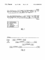
44 Claims, 8 Drawing Sheets
(List continued on neXt page.)
___________________ "an"
CmeData bus
XA CPU Core
Pmgram bus
SFR bus
26
24
DAT
bus
semi:
L
77
Parts 03
61/L__|
22
US 6,728,892 B1
Page 2
US. PATENT DOCUMENTS
6,457,082 B1 *
9/2002 Zhang et a1. ............. .. 710/260
6,463,542 B1 * 10/2002 Yu et a1. ................... .. 713/320
6,324,597 B2 * 11/2001
6,370,599 B1 *
Collier ...................... .. 710/22
4/2002 Anand et a1. ............... .. 710/15
* cited by examiner
U.S. Patent
Apr. 27, 2004
Sheet 3 0f 8
US 6,728,892 B1
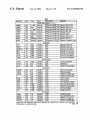
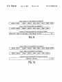
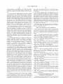
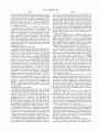
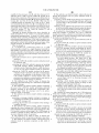
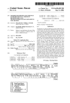
MMRs
MMR name
1 RM? I Reset
[Access
[Address Otisei
[Description
Message Object Registers (n = U - 31}
MnMtDH
R/W
x....x00b
Word only
MnMllJL
MnMSKH
MnMSKL
xxxxh
Word only
x....xl]i)t1b Word only
xxxxh
Word only
MnFCR
R/W
R/W
R/W
R/W
R/W
R/W
R/W
MCPLL
MCPLH
CANINTELC
MClR
ttttttn4ngngn1ngb00tlbtn0hi MessagenMatohlt] High
MessagenMateh it] Low
MessagenMaslr High
MessagenMaskLow
MessagenControl
MessagenBuitertooation
MessagenButter Size
MessagenFragmentation Count
R/C
RiC
R/C
R0
00Dn4n3ngn1ng00tttbm2h)
tttitln4n3ngn1ngtlt0tlbln4ht
?itttnangngning?ttttbmtiht
00000xxxb Byte/Word 000n4n3n2n1ngt000bm8h)
xxxxh
Word only
000n4n3ngningt0t0blnAh)
00000xxxb Byte/Word 0U0it4tl3ii2it1itgtt00bl?0h)
UUXXXXXXD Byte/Word
UDOtt4tt3ii2tttitg1110btnEh)
CiC Registers
tltitltih
Byte/Word
224h
tttltltth
Byte/Word
22Eh
tibtiOh
Byte/Word
22Bh
OOOtih
Byte/Word
229h
MElR
R0 -
0000b
Byte/Word
22Ah
Message Error into Register
FESTR
FEENR
R/C
R/W
ittltttth
0000b
Byte/Word
Byte/Word
22Ch
22Eh
Frame Error Status Register
Frame Error Enable Register
MnCTt
MnBLR
MnBSZ
Message Complete Low
Message Complete High
CAN Interrupt Flag Register
Message Complete Into Reg.
SCP/SPI Registers
SPtCFG
SPlDAiA
SPICS
RAN
R/W
R/W
0000b
tJiih
00h
CANCMR
CANSTR
CANBiR
R/W
RIC
R/W
TXERC
RXERC
EWLR
ECCR
ALCR
RTXDTM
GCTL
Byte/Word
Byte/Word
Byte/Word
SCPiSPt Contiguration
SCPISPI Data
SCP/SPt Control and Status
lith
00h
00h
2Bi1h
262h
263h
CCB Registers
Byte/Word
27Ch
Byte/Word
27th
Byte/Word
272h
R/W
R/W’
R/W’
00h
00h
00h
Byte/Word
Byte/Word
Byte/Word
273h
271th
275h
CAN Bus Timing Reg. (high)
Tx Error Counter
Rx Error Counter
R/W
RC
R0
WC
R/W
95h
0000b
0000b
OOOBh
0000h
Byte/Word
Byte/Word
Byte/Word
Byte/Word
Byte/Word
27Ch
27Ch
27Ah
27Ch
27Eh
Error Warning Limit Register
Error Code Capture Register
Arbitration Lost Capture Reg.
RTX Data Test Mode
Global Control Byte
CAN Command Register
CAN Status Register
CAN Bus Timing Reg. (low)
MtFRegisters
XRAMB
MBXSR
MIFBTRL
MtFBiRH
R/W
R/W
R/W
R/W
FEh
FFh
EFh
Fth
Byte/Word
Byte/Word
Byte/Word
Bwword
290h
29th
292h
293h
XRAM Base Address
Msg. Buii/XRAM Seg. Reg.
MtF Bus Timing Reg. Low
MtF Bus timing Reg. High
Legend:R/W=Read&Wrtte. R0=Read Only. W0=Write0n|y, R/C=Reao&Clear, W'=Wriiahle only during
CAN Reset mode, it = undetined atter reset.
4
-
U.S. Patent
Apr. 27, 2004
Sheet 4 0f 8
US 6,728,892 B1
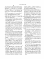
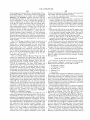
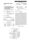
Data Memory Segment 0
OOFFFFh .LLLLLLIF
Off-Chip
4K Bytes
MMR Space
[1111111 MMR Base Address
Off-Chip
512 BytesT
XRAM
J H 1 r r r 1
XRAM Base Address
Off-Chip
OOUBFFh .LLLILLLJ
Off-Chip Data Memory
(Scratch Pad)
FI'I'ITH'I' DOOOOOh
MMR Space
Offset FFFh -—-—+
Offset 1 FFh —-—>
512 Bytes Object Registers
|~—-- <-—- Offset OOOh
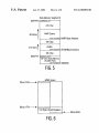
U.S. Patent
Apr. 27, 2004
Sheet 5 of 8
US 6,728,892 B1
Segment xy in Data
Memory Space
xyFFFFh ,_____I
Object n
Buffer Size
Object n Message Buffer
323
316 315
|—“'—— 4-—— MBXSRUIU]
30
MHBLR
XRAM
512 Bytes
e23
e16 a15
a8 a7
a0
I___''' <— MBXSRUzO] XRAMB[7:1]0
00h
1-‘ "'_' xyOOOOh
Segment xy in Data
Memory Space
xyFFFFh ___'._J
e23
_
a16 e15
<— MBXSRUD]
a0
MnBLR
OmectnT Obiect n Message Buffer
XRAM
512 BYTES
Buffer size
J
XRAM
e23
e16 e15
a8 a7
J—_<— MBXSR[7:0] XRAMB[7:1]0
l—_'
"xy0000h
a0
00h
U.S. Patent
Apr. 27, 2004
Sheet 6 of 8
US 6,728,892 B1
Dbiect n Match ID Field (MnMlDH and MnMlDL)
Mid28-Mid18
Mid17—Mid10 MidQ-MidZ Midi
MidO
MIDE
Object n Mask Field (MnMSKH and MnMSKL)
MSk28 — Msk18
MsklT ' MSk10
Msk9 ~ Msk2
Mskl
MskD
Screener ID Field (assembled from incoming bit-stream)
DAN |D.28 — CAN lD.18 Data Byte 1 [7:0] Data Byte 2 [7:0]
X
IDE
Midi)
MIDE
X
Object n Match ID Field (MHMIDH and MnMlDL)
Midl
Mid28- Mid18
Mid17 — Mid10
Mid9 — Mid2
Object n Mask Field (MnMSKH and MnMSKL)
Msk28 - MsklB
Msk17 — Mskl 0
Msk9 — Msk2
Mski
MskD
Screener ID Field (assembled from incoming bit-stream)
CAN ID.28 — CAN lD.0
FIG. 10
IDE
U.S. Patent
Apr. 27, 2004
Sheet 7 of 8
US 6,728,892 B1
Benn
tté?ét‘éttéF
Data Byte 2
Data Byte 3
ADDRESS
Data Byte DLC
Data Byte 2 (next)
Data Byte 3 (next)
FIG. 11
Framelmo
Data Byte 1
Data Byte 2
Data Byte DLC
Framelnto (next)
Data Byte 1 (next)
Data Byte 2 (next)
FIG. 12
DIRECTION OF
INCREASING
ADDRESS
U.S. Patent
Apr. 27, 2004
Sheet 8 of 8
US 6,728,892 B1
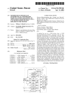
{91
sEEERck1
E
SLEEPOkn
IOLEMOOE
SLEEP-ENABLE
CCb_lDLE_n
AND
NO RX
95
97
AsYNcHRONOus
LATCH
”\~9O
RX
93
I
OMA
ENGINE
r/
N
38
TX
LOGIC
MESSAGE
POINTER
77
m
‘05
x107
HANDLER
MESSAGE K103
MANAGEMENT
TX PRE-
“101
ARBITRATION
CAN/CAL MODULE
FIG. 14
US 6,728,892 B1
1
2
METHOD FOR CONSERVING POWER IN A
CAN MICROCONTROLLER AND A CAN
MICROCONTROLLER THAT IMPLEMENTS
THIS METHOD
of high performance 16-bit single-chip microcontrollers. It
is believed that the XA-C3 is the ?rst chip that features
hardWare CAL support.
The XA-C3 is a CMOS 16-bit CAL/CAN 2.0B micro
controller that incorporates a number of different inventions,
including the present invention. These inventions include
This application claims the full bene?t and priority of
US. Provisional Application Serial No. 60/154,022, ?led on
novel techniques and hardWare for ?ltering, buffering,
handling, and processing CAL/CAN messages, including
Sep. 15, 1999, the disclosure of Which is fully incorporated
herein for all purposes.
the automatic assembly of multi-frame fragmented mes
10
BACKGROUND OF THE INVENTION
The present invention relates generally to the ?eld of data
communications, and more particularly, to the ?eld of serial
communications bus controllers and microcontrollers that
incorporate the same.
sages With minimal CPU intervention, as Well as for man
aging the storage and retrieval of the message data, and the
memory resources utiliZed therefor.
The present invention relates to a poWer conservation
scheme that enables one or more hardWare components of
15
CAN (Control Area Network) is an industry-standard,
the microcontroller, e.g., the CPU core, to remain in a sleep
or idle mode While other hardWare components, e.g., CAL/
tWo-Wire serial communications bus that is Widely used in
CAN hardWare components, are active, e.g., automatically
automotive and industrial control applications, as Well as in
assembling a multi-frame, fragmented message.
medical devices, avionics, office automation equipment,
consumer appliances, and many other products and appli
SUMMARY OF THE INVENTION
cations. CAN controllers are currently available either as
stand-alone devices adapted to interface With a microcon
troller or as circuitry integrated into or modules embedded
The present invention encompasses a method for con
serving poWer in a CAN microcontroller that includes a
in a microcontroller chip. Since 1986, CAN users (softWare
processor core and a CAN/CAL module that includes a
the CAN While employing the CAN physical layer and the
CAN frame format, and adhering to the CAN speci?cation.
CALs have heretofore been implemented primarily in
softWare, With very little hardWare CAL support.
Consequently, CALs have heretofore required a great deal of
plurality of sub-blocks that cooperatively function to process
incoming CAL/CAN messages, Which method includes the
steps of placing the processor core in a poWer-reduction
mode of operation (e.g., a sleep or idle mode of operation),
placing the CAN/CAL module in a poWer-reduction mode of
operation, and activating the CAN/CAL module to process
an incoming CAL/CAN message (e.g., to perform automatic
hardWare assembly of a multi-frame, fragmented CAL/CAN
host CPU intervention, thereby increasing the processing
message), thereby terminating the poWer-reduction mode of
overhead and diminishing the performance of the host CPU.
operation thereof, While the processor core is in its poWer
programmers) have developed numerous high-level CAN
25
Application Layers (CALs) Which eXtend the capabilities of
Thus, there is a need in the art for a CAN hardWare 35 reduction mode of operation.
implementation of CAL functions normally implemented in
In a preferred embodiment, the method further includes
softWare in order to offload these tasks from the host CPU
host CPU processing resources and a commensurate
the steps of generating a message-complete interrupt in
response to completion of assembly of the multi-frame,
fragmented CAL/CAN message, and activating the proces
improvement in host CPU performance. One of the most
demanding and CPU resource-intensive CAL functions is
message management, Which entails the handling, storage,
particular preferred embodiment, the method further
includes the steps of repeating the step of placing the
to the CAN hardWare, thereby enabling a great savings in
sor core in response to the message-complete interrupt. In a
and processing of incoming CAL/CAN messages received
CAN/CAL module in a poWer-reduction mode of operation
and the activating step, in seriatim, a plurality of times,
over the CAN serial communications bus and/or outgoing
CAL/CAN messages transmitted over the CAN serial com
45
While the processor core is in its poWer-reduction mode of
munications bus. CAL protocols, such as DeviceNet,
operation.
CANopen, and OSEK, deliver long messages distributed
In a present speci?c implementation, the step of placing
the CAN/CAL module in a poWer-reduction mode operation
is performed by a poWer or sleep control module contained
Within the CAN/CAL module, in the folloWing manner.
over many CAN frames, Which methodology is sometimes
referred to as “fragmented” or “segmented” messaging. The
process of assembling such fragmented, multi-frame mes
sages has heretofore required a great deal of host CPU
intervention. In particular, CAL softWare running on the host
CPU actively monitors and manages the buffering and
processing of the message data, in order to facilitate the
assembly of the message fragments or segments into com
Particularly, ?rst logic circuitry associated With each of the
plurality of sub-blocks generates a respective ?rst signal
having a ?rst logic level if that sub-block is currently active,
and having a second logic level if that sub-block is not
55
plete messages.
Based on the above and foregoing, it can be appreciated
that there presently eXists a need in the art for a hardWare
implementation of CAL functions normally implemented in
softWare in order to offload these tasks from the host CPU,
thereby enabling a great savings in host CPU processing
resources and a commensurate improvement in host CPU
performance.
The assignee of the present invention has recently devel
oped a neW microcontroller product, designated “XA-C3”,
that ful?lls this need in the art. The XA-C3 is the neWest
member of the Philips XA (extended Architecture) family
65
currently active. Second logic circuitry generates a second
signal having a ?rst logic level if any of the ?rst signals are
at the ?rst logic level, and having a second logic level in
response to all of the ?rst signals having the second logic
level. Third logic circuitry generates a third signal having a
?rst logic level if the processor core is not idle, and having
a second logic level if the processor core is idle. Fourth logic
circuitry generates a fourth signal having a ?rst logic level
if an incoming message is being received, and having a
second logic level if an incoming message is not being
received. Fifth logic circuitry generates a clock disable
signal in response to the second, third, and fourth signals all
being at their respective second logic level. SiXth logic
US 6,728,892 B1
3
4
circuitry disables a clock applied to the CAN/CAL module
in response to the clock disable signal to thereby place the
CAN/CAL module in the poWer-reduction mode of opera
tion.
doWn mode of operation, and can be Woken up over a
prescribed Wake-up period When in the poWer-doWn mode
of operation.
In a speci?c implementation, the placing step is per
formed by determining Whether the CAN/CAL module is
ready to be placed into the poWer-doWn mode of operation,
In a present speci?c implementation, the step of placing
the processor core in a poWer-reduction mode of operation
is performed by a poWer or sleep control module contained
Within the CAN/CAL module, in the following manner.
Particularly, a ?rst logic portion of the poWer control module
generates a clock disable signal having a ?rst logic level if
the processor core has pending interrupts, and having a
second logic level if the processor core has no pending
interrupts, and a second logic portion of the poWer control
and stopping a main system clock in response to a determi
nation that the CAN/CAL module is ready to be placed into
the poWer-doWn mode of operation. Further, in the speci?c
10
or a system reset command.
module disables a clock applied to the processor core in
response to the clock disable signal, to thereby place the
processor core in the poWer-reduction mode of operation.
The present invention, in another of its aspects, encom
15
the above-discussed methods.
BRIEF DESCRIPTION OF THE DRAWINGS
troller that includes a processor core and a CAN/CAL
These and various other aspects, features, and advantages
of the present invention Will be readily understood With
reference to the folloWing detailed description of the inven
tion read in conjunction With accompanying draWings, in
module, Which method includes the steps of placing the
processor core in a poWer-reduction mode of operation (e.g.,
a sleep or idle mode of operation), While the CAN/CAL
module is actively processing an incoming CAL/CAN mes
sage (e.g., to perform automatic hardWare assembly of a
25
nating the poWer-reduction mode of operation in response to
an interrupt.
In a preferred embodiment, the CAN/CAL module auto
messages While the processor core remains in its poWer
XA-C3 microcontroller;
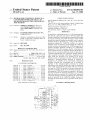
FIG. 4 is a table listing all of the Memory Mapped
reduction mode of operation, and the CAN/CAL module
generates a message-complete interrupt in response to
Registers (MMRs) provided by the XA-C3 microcontroller;
completion of assembly of the multi-frame, fragmented
35
the processor core in a poWer-reduction mode of operation
is performed by a poWer or sleep control module contained
Within the CAN/CAL module, in the folloWing manner.
FIG. 5 is a illustrating the mapping of the overall data
memory space of the XA-C3 microcontroller;
FIG. 6 is a diagram illustrating the MMR space contained
Within the overall data memory space of the XA-C3 micro
controller;
Particularly, a ?rst logic portion of the poWer control module
generates a clock disable signal having a ?rst logic level if
the processor core has pending interrupts, and having a
second logic level if the processor core has no pending
interrupts, and a second logic portion of the poWer control
Which:
FIG. 1 is a diagram illustrating the format of a Standard
CAN Frame and the format of an Extended CAN Frame;
FIG. 2 is a diagram illustrating the interleaving of CAN
Data Frames of different, unrelated messages;
FIG. 3 is a high-level, functional block diagram of the
matically assembles incoming, multi-frame, fragmented
message, Whereby the terminating step is executed in
response to the message-complete interrupt.
In a present speci?c implementation, the step of placing
In yet other aspects, the present invention encompasses a
CAN microcontroller that implements any one or more of
passes a method for conserving poWer in a CAN microcon
multi-frame, fragmented CAL/CAN message), and termi
implementation, the method further includes the step of
terminating the poWer-doWn mode of operation of the entire
CAN microcontroller, including both the processor core and
the CAN/CAL module, in response to an external interrupt
45
module disables a clock applied to the processor core in
FIG. 7 is a diagram illustrating formation of the base
address of the on-chip XRAM of the XA-C3
microcontroller, With an object n message buffer mapped
into off-chip data memory;
FIG. 8 is a diagram illustrating formation of the base
address of the on-chip XRAM of the XA-C3
microcontroller, With an object n message buffer mapped
into the on-chip XRAM;
response to the clock disable signal, to thereby place the
processor core in the poWer-reduction mode of operation.
In yet another of its aspects, the present invention encom
FIG. 9 is a diagram illustrating the Screener ID Field for
a Standard CAN Frame;
FIG. 10 is a diagram illustrating the Screener ID Field for
passes a method for conserving poWer in a CAN microcon
troller that includes a processor core and a CAN/CAL
an Extended CAN Frame;
module, Which method includes the steps of placing the
entire CAN microcontroller, including both the processor
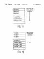
FIG. 11 is a diagram illustrating the message storage
format for fragmented CAL messages;
FIG. 12 is a diagram illustrating the message storage
format for fragmented CAN messages;
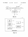
FIG. 13 is a partial schematic, partial functional block
diagram of a sleep control module incorporated Within the
XA-C3 microcontroller in accordance With the present
core and the CAN/CAL module in a poWer-doWn mode of
operation, detecting receipt of an incoming message, and
55
activating the CAN/CAL module in response to the detect
ing step to process the incoming message (e.g., to perform
automatic hardWare assembly of a multi-frame, fragmented
CAL/CAN message), thereby terminating the poWer-doWn
invention; and,
mode of operation of the CAN/CAL module, Without ter
minating the poWer-doWn mode of operation of the proces
FIG. 14 is a high-level block diagram depicting the
CAN/CAL module of the XA-C3 microcontroller, and its
constituent sub-blocks.
sor core.
In a preferred embodiment, the method further includes
the step of placing the processor core in a poWer-reduction
mode of operation (e.g., a sleep or idle mode of operation)
in response to the detecting step. The processor core can be
substantially instantaneously Woken up When in the power
65
DETAILED DESCRIPTION OF THE
PREFERRED EMBODIMENT
The present invention is described beloW in the context of
a particular implementation thereof, i.e., in the context of the
US 6,728,892 B1
6
5
XA-C3 microcontroller manufactured by Philips Semicon
fragmented message are not typically transmitted in a
ductors. Of course, it should be clearly understood that the
present invention is not limited to this particular
contiguous fashion, but rather, the individual CAN
Frames of different, unrelated messages are interleaved on
the CAN bus, as is illustrated in FIG. 2
implementation, as any one or more of the various aspects
and features of the present invention disclosed herein can be
utiliZed either individually or any combination thereof, and
in any desired application, e.g., in a stand-alone CAN
5
controller device or as part of any other microcontroller or
system.
The folloWing terms used herein in the context of describ
10
ing the preferred embodiment of the present invention (i.e.,
Fragmented Message: A lengthy message (in excess of 8
bytes) divided into data packets and transmitted using a
sequence of individual CAN Frames. The speci?c Ways
that sequences of CAN Frames construct these lengthy
messages is de?ned Within the context of a speci?c CAL.
The XA-C3 microcontroller automatically re-assembles
these packets into the original, lengthy message in hard
Ware and reports (via an interrupt) When the completed
the XA-C3 microcontroller) are de?ned as folloWs:
Standard CAN Frame: The format of a Standard CAN Frame
(re-assembled) message is available as an associated
Receive Message Object.
is depicted in FIG. 1.
Extended CAN Frame: The format of an Extended CAN 15 Message Buffer: A block of locations in XA Data memory
Frame is also depicted in FIG. 1.
Where incoming (received) messages are stored or Where
Acceptance Filtering: The process a CAN device imple
outgoing (transmit) messages are staged.
MMR: Memory Mapped Register. An on-chip command/
ments in order to determine if a CAN frame should be
control/status register Whose address is mapped into XA
accepted or ignored and, if accepted, to store that frame in
a pre-assigned Message Object.
Message Object: A Receive RAM buffer of pre-speci?ed
siZe (up to 256 bytes for CAL messages) and associated
20
With a particular Acceptance Filter or, a Transmit RAM
buffer Which the User preloads With all necessary data to
transmit a complete CAN Data Frame. AMessage Object
bits control global parameters that apply to all Message
25
can be considered to be a communication channel over
Which a complete message, or a succession of messages,
can be transmitted.
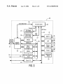
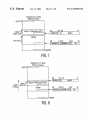
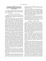
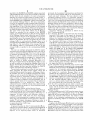
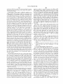
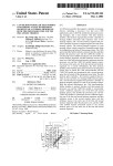
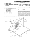
high-level block diagram of the XA-C3 microcontroller 20.
The XA-C3 microcontroller 20 includes the folloWing func
tional blocks that are fabricated on a single integrated circuit
30
an XA CPU Core 22, that is currently implemented as a
Acceptance Filtering for CAN Frame reception and
35
message Which is then used in Acceptance Filtering. The
mented as a 32K ROM/EPROM, and that is
bits are the information quali?ed by Acceptance Filtering.
40
the incoming Screener ID is compared. Individual Match
IDs for each of 32 Message Objects are programmed by
the user into designated Memory Mapped Registers
(MMRs).
Mask: A 29-bit ?eld pre-speci?ed by the user Which can
16-bit fully static CPU With 24-bit program and data
address range, that is upWardly compatible With the
80C51architecture, and that has an operating frequency
of up to 30 MHZ;
a program or code memory 24 that is currently imple
Screener ID includes the CAN Arbitration ID and the IDE
bit, and can include up to 2 Data Bytes. These 30 extracted
Match ID: A 30-bit ?eld pre-speci?ed by the user to Which
(IC) chip packaged in a 44-pin PLCC or a 44-pin LQFP
package:
in the CAN Frame Header. This ID ?eld is used to
arbitrate Frame access to the CAN bus. Also used in
Transmit Pre-Arbitration.
Screener ID: A 30-bit ?eld extracted from the incoming
Objects.
With reference noW to FIG. 3, there can be seen a
CAN Arbitration ID: An 11-bit (Standard CAN 2.0Frame) or
29-bit (Extended CAN 2.0B Frame) identi?er ?eld placed
Data memory space and is accessed as Data memory by
the XAprocessor. With the XAC-3 microcontroller, a set
of eight dedicated MMRs are associated With each Mes
sage Object. Additionally, there are several MMRs Whose
45
override (Mask) a Match ID comparison at any particular
bit (or, combination of bits) in an Acceptance Filter.
Individual Masks, one for each Message Object, are
programmed by the user in designated MMRs. Individual
Mask patterns assure that single Receive Objects can
Screen for multiple acknoWledged CAL/ CAN Frames and
thus minimiZe the number of Receive Objects that must
be dedicated to such loWer priority Frames. This ability to
Mask individual Message Objects is an important neW
50
CAL feature.
55
bi-directionally coupled to the XA CPU Core 22 via an
internal Program bus 25. A map of the code memory
space is depicted in FIG. 4;
a Data RAM 26 (internal or scratch pad data memory) that
is currently implemented as a 1024 Byte portion of the
overall XA-C3 data memory space, and that is
bi-directionally coupled to the XA CPU Core 22 via an
internal DATA bus 27;
an on-chip message buffer RAM or XRAM 28 that is
currently implemented as a 512 Byte portion of the
overall XA-C3 data memory space Which may contain
part or all of the CAN/CAL (Transmit & Receive
Object) message buffers;
a Memory Interface (MIF) unit 30 that provides interfaces
to generic memory devices such as SRAM, DRAM,
CAL: CAN Application Layer. A generic term for any
high-level protocol Which extends the capabilities of CAN
While employing the CAN physical layer and the CAN
frame format, and Which adheres to the CAN speci?ca
tion. Among other things, CALs permit transmission of
Messages Which exceed the 8 byte data limit inherent to
CAN Frames. This is accomplished by dividing each
?ash, ROM, and EPROM memory devices via an
external address/data bus 32, via an internal Core Data
bus 34, and via an internal MMR bus 36;
a DMA engine 38 that provides 32 CAL DMA Channels;
a plurality of on-chip Memory Mapped Registers
(MMRs) 40 that are mapped to the overall XA-C3 data
memory space—a 4K Byte portion of the overall
XA-C3 data memory space is reserved for MMRs.
message into multiple packets, With each packet being
These MMRs include 32 (Message) Object or Address
transmitted as a single CAN Frame consisting of a maxi
mum of 8 data bytes. Such messages are commonly 65
referred to as “segmented” or “fragmented” messages.
Pointers and 32 ID Screeners or Match IDs, corre
The individual CAN Frames constituting a complete
sponding to the 32 CAL Message Objects. A complete
listing of all MMRs is provided in the Table depicted in
FIG. 5;
US 6,728,892 B1
8
7
alWays start at a 4K boundary. The reset values for MRBH
and MRBL are 0Fh and FOh, respectively. Therefore, after a
a 2.0B CAN/DLL Core 42 that is the CAN Controller
Core from the Philips SJA1000QAN (2.0A/B) Data
Link Layer (CDLL) device (hereinafter referred to as
reset, the MMR space is mapped to the uppermost 4K Bytes
the “CAN Core Block” (CCB)); and,
of Data Segment 0Fh, but access to the MMRs 40 is
disabled. The ?rst 512 Bytes (offset 000h—1FFh) of MMR
space are the Message Object Registers (eight per Message
an array of standard microcontroller peripherals that are
bi-directionally coupled to the XA CPU Core 22 via a
Special Function Register (SFR) bus 43. These stan
dard microcontroller peripherals include Universal
Asynchronous Receiver Transmitter (UART) 49, an
SPI serial interface (port) 51, three standard timers/
counters With toggle output capability, namely, Timer 0
& Timer 1 included in Timer block 53, and Timer 2
included in Timer block 54, a Watchdog Timer 55, and
four 8-bit I/O ports, namely, Ports 0—3 included in
block 61, each of Which has 4 programmable output
Object) for objects n=0—31, as is shoWn in FIG. 6.
The base address of the XRAM 28 is determined by the
10
contents of the MMRs designated MBXSR and XRAMB, as
is shoWn in FIGS. 7 and 8. As previously mentioned, the 512
Byte XRAM 28 is Where some (or all) of the 32 (Rx/Tx)
message buffers (corresponding to Message Objects
n=0—31) reside. The message buffers can be extended off
15
con?gurations.
chip to a maximum of 8 KBytes. This off-chip expansion
capability can accommodate up to thirty-tWo, 256-Byte
message buffers. Since the uppermost 8 bits of all message
The DMA engine 38, the MMRs 40, and the CCB 42 can
collectively be considered to constitute a CAN/CAL module
77, and Will be referred to as such at various times through
buffer addresses are formed by the contents of the MBXSR
register, the XRAM 28 and all 32 message buffers must
reside in the same 64K Byte data memory segment. Since
out the folloWing description. Further, the particular logic
the XA-C3 microcontroller 20 only provides address lines
A0—A19 for accessing external memory, all external
memory addresses must be Within the loWest 1 MByte of
address space. Therefore, if there is external memory in the
system into Which any of the 32 message buffers Will be
mapped, then all 32 message buffers and the XRAM 28 must
also be mapped entirely into that same 64K Byte segment,
Which must be beloW the 1 MByte address limit.
elements Within the CAN/CAL module 77 that perform
“message management” and “message handling” functions
Will sometimes be referred to as the “message management
engine” and the “message handler”, respectively, at various
times throughout the folloWing description. Other nomen
25
clature Will be de?ned as it introduced throughout the
folloWing description.
As previously mentioned, the XA-C3 microcontroller 20
automatically implements, in hardWare, many message man
agement and other functions that Were previously only
implemented in softWare running on the host CPU (or not
After the memory space has been mapped, the user can
set-up or de?ne up to 32 separate Message Objects, each of
Which can be either a Transmit (TX) or a Receive (Rx)
Message Object. A Rx Message Object can be associated
implemented at all), including transparent, automatic
either With a unique CAN ID, or With a set of CAN IDs
re-assembly of up to 32 concurrent, interleaved, multi
frame, fragmented CAL messages. For each application that
Which share certain ID bit ?elds. As previously mentioned,
each Message Object has its oWn reserved block of data
is installed to run on the host CPU (i.e., the XA CPU Core 35 memory space (up to 256 Bytes), Which is referred to as that
Message Object’s message buffer. As Will be seen, both the
siZe and the base address of each Message Object’s message
buffer is programmable.
As previously mentioned, each Message Object is asso
22), the user (softWare programmer) must set-up the hard
Ware for performing these functions by programming certain
ones of the MMRs and SFRs in the manner set forth in the
XA-C3 Functional Speci?cation and XA-C3 CAN Transport
Layer Controller User Manual. The register programming
ciated With a set of eight MMRs 40 dedicated to that
procedures that are most relevant to an understanding of the
present invention are described beloW, folloWed by a
Message Object. Some of these registers function differently
for TX Message Objects than they do for Rx Message
Objects. These eight MMRs 40 are designated “Message
description of the various message management and other
functions that are automatically performed by the CAL/
CAN module 77 during operation of the XA-C3 microcon
troller 20 after it has been properly set-up by the user.
Object Registers” (see FIG. 4).
45
1. MnMIDH Message n Match ID High
FolloWing these sections, a more detailed description of the
particular invention to Which this application is directed is
. MnMIDL Message n Match ID LoW
. MnMSKH Message n Mask High
provided.
. MnMSKL Message n Mask LoW
Set-up/Programming Procedures
. MnCTL Message n Control
As an initial matter, the user must map the overall XA-C3
data memory space, as illustrated in FIG. 5. In particular,
subject to certain constraints, the user must specify the
starting or base address of the XRAM 28 and the starting or
base address of the MMRs 40. The base address of the
The names of these eight MMRs 40 are:
. MnBLR Message n Buffer Location Register
. MnBSZ Message n Buffer SiZe
8. MnFCR Message n Fragment Count Register
55
Where n ranges from 0 to 31 (i.e., corresponding to 32
MMRs 40 can be speci?ed by appropriately programming
Special Function Registers (SFRs) MRBL and MRBH. The
independent Message Objects).
base address of the XRAM 28 can be speci?ed by appro
by con?guring (programming) some or all of the eight
priately programming the MMRs designated MBXSR and
XRAMB (see FIG. 4).
MMRs dedicated to that Message Object, as Will be
described beloW. Additionally, as Will be described beloW,
The user can place the 4 KByte space reserved for MMRs
the user must con?gure (program) the global GCTL register,
Whose bits control global parameters that apply to all
40 anyWhere Within the entire 16 Mbyte data memory space
supported by the XA architecture, other than at the very
bottom of the memory space (i.e., the ?rst 1 KByte portion,
starting address of 000000h), Where it Would con?ict With
In general, the user de?nes or sets up a Message Object
Message Objects.
In particular, the user can specify the Match ID value for
the on-chip Data RAM 26 that serves as the internal or
each Message Object to be compared against the Screener
IDs extracted from incoming CAN Frames for Acceptance
scratch-pad memory. The 4 KBytes of MMR space Will
Filtering. The Match ID value for each Message Object n is
65
US 6,728,892 B1
9
10
speci?ed in the MnMIDH and MnMIDL registers associated
previously, the Acceptance Filtering process performed by
With that Message Object n. The user can mask any Screener
ID bits Which are not intended to be used in Acceptance
“match and mask” technique. The basic objective of this
Filtering, on an object-by-object basis, by Writing a logic ‘1’
in the desired (to-be-masked) bit position(s) in the appro
priate MnMSKH and/or MNMSKL registers associated With
each particular Message Object n. The user is responsible,
Acceptance Filtering process is to determine Whether a
Screener ID ?eld of the received CAN Frame (eXcluding the
“don’t care” bits masked by the Mask ?eld for each Message
Object) matches the Match ID of any enabled one of the 32
on set-up, for assigning a unique message buffer location for
each Message Object n. In particular, the user can specify the
least signi?cant 16 bits of the base address of the message
Message Objects that has been designated a Receive Mes
the XA-C3 microcontroller 20 can be characteriZed as a
10
buffer for each particular Message Object n by programming
the MnBLR register associated With that Message Object n.
The upper 8 bits of the 24-bit address, for all Message
Objects, are speci?ed by the contents of the MBXSR
register, as previously discussed, so that the message buffers
for all Message Objects reside Within the same 64 KByte
memory segment. The user is also responsible, on set-up, for
specifying the siZe of the message buffer for each Message
Object n. In particular, the user can specify the siZe of the
message buffer for each particular Message Object n by
programming the MnBSZ register associated With that Mes
sage Object n. The top location of the message buffer for
each Message Object n is determined by the siZe of that
message buffer as speci?ed in the corresponding MnBSZ
register.
sage Object. If there is a match betWeen the received CAN
Frame and more than one Message Object, then the received
CAN Frame Will be deemed to have matched the Message
Object
Acceptance
With theFiltering
loWest object
is performed
number as folloWs by the
XA-C3 microcontroller 20:
15
(1) A Screener ID ?eld is eXtracted from the incoming
(received) CAN Frame. In this regard, the Screener ID
?eld that is assembled from the incoming bit stream is
different for Standard and EXtended CAN Frames. In
particular, as is illustrated in FIG. 9, the Screener ID ?eld
for a Standard CAN Frame is 28 bits, consisting of 11
CAN ID bits eXtracted from the header of the received
CAN Frame +2><8 (16) bits from the ?rst and second data
bytes (Data Byte 1 and Data Byte 2) of the received CAN
Frame +the IDE bit. Thus, the user is required to set the
25
Mskl and Msk0 bits in the Mask Field (MnMSKL
register) for Standard CAN Frame Message Objects, i.e.,
The user can con?gure (program) the MnCTL register
associated With each particular Message Object n in order to
enable or disable that Message Object n, in order to de?ne
to “don’t care”. In addition, in many applications based on
Standard CAN Frames, either Data Byte 1, Data Byte 2,
or designate that Message Object n as a TX or RX Message
Object; in order to enable or disable automatic hardWare
or both do not participate in Acceptance Filtering. In those
assembly of fragmented RX messages (i.e., automatic frag
mented message handling) for that Message Object n; in
Byte(s). The IDE bit is not maskable. As is illustrated in
FIG. 10, the Screener ID ?eld for an EXtended CAN
order to enable or disable automatic generation of a
Frame is 30 bits, consisting of 29 CAN ID bits eXtracted
applications, the user must also mask out the unused Data
Message-Complete Interrupt for that Message Object n; and,
Remote Transmit Request (RTR) handling. In CANopen and
from the header of the incoming CAN Frame +the IDE
bit. Again, the IDE bit is not maskable.
(2) The assembled Screener ID ?eld of the received CAN
OSEK systems, the user must also initialiZe the MnFCR
Frame is then sequentially compared to the corresponding
register associated With each Message Object n.
Match ID values speci?ed in the MnMIDH and MnMIDL
in order to enable or not enable that Message Object n for
35
registers for all currently enabled Receive Message
As previously mentioned, on set-up, the user must con
?gure (program) the global GCTL register, Whose bits
control global parameters that apply to all Message Objects.
Objects. Of course, any bits in the Screener ID ?eld that
are masked by a particular Message Object are not
included in the comparison. That is, if there is a ‘1’ in a
In particular, the user can con?gure (program) the GCTL
register in order to specify the high-level CAL protocol (if
any) being used (e.g., DeviceNet, CANopen, or OSEK); in
order to enable or disable automatic acknowledgment of
45
CANopen Frames (CANopen auto-acknoWledge); and, in
care”, i.e., alWays yields a match With the corresponding
order to specify Which of tWo transmit (TX) pre-arbitration
schemes/policies is to be utiliZed (i.e., either TX pre
arbitration based on CAN ID, With the object number being
bit of the Screener ID of the received CAN Frame.
(3) If the above comparison process yields a match With
more than one Message Object, then the received CAN
Frame Will be deemed to have matched the Message
used as a secondary tie-breaker, or TX pre-arbitration based
on object number only).
Receive Message Objects and the Receive Process
During reception (i.e., When an incoming CAN Frame is
being received by the XA-C3 microcontroller 20), the CAN/
CAL module 77 Will store the incoming CAN Frame in a
Object having the loWest object number
Message Storage:
55
temporary (13-Byte) buffer, and determine Whether a
complete, error-free CAN frame has been successfully
Each incoming (received) CAN Frame that passes Accep
tance Filtering, Will be automatically stored, via the DMA
engine 38, into the message buffer for the Receive Message
Object that particular CAN Frame Was found to have
matched. In an eXemplary implementation, the message
buffers for all Message Objects are contained in the XRAM
28.
received. If it is determined that a complete, error-free CAN
Frame has been successfully received, then the CAN/CAL
module 77 Will initiate Acceptance Filtering in order to
Message Assembly:
determine Whether to accept and store that CAN Frame, or
to ignore/discard that CAN Frame.
In general, the DMA engine 38 Will transfer each accepted
CAN Frame from the 13-byte pre-buffer to the appropriate
Acceptance Filtering
In general, because the XA-C3 microcontroller 20 pro
vides the user With the ability to program separate Match ID
bit position of the Mask ?eld speci?ed in the MnMSKH
and Mn MSKL registers for a particular Message Object,
then the corresponding bit position in the Match ID ?eld
for that particular Message Object becomes a “don’t
65
message buffer (e.g., in the XRAM 28), one Word at a time,
starting from the address pointed to by the contents of the
and Mask ?elds for each of the 32 independent Message
MBXSR and MnBLR registers. Every time the DMA engine
Objects, on an object-by-object basis, as described
38 transfers a byte or a Word, it has to request the bus. In this
US 6,728,892 B1
11
12
regard, the MIF unit 30 arbitrates between accesses from the
XA CPU Core 22 and from the DMA engine 38. In general,
byte (Data Byte 1) of each received CAN Frame that
matches that particular Receive Message Object Will be used
bus arbitration is done on an “alternate” policy. After a DMA
to encode fragmentation information only, and thus, Will not
be stored in the message buffer for that particular Receive
bus access, the XA CPU Core 22 Will be granted bus access,
if requested. After an XA CPU bus access, the DMA engine
Message Object. Thus, message storage for such “FRAG
enabled” Receive Message Objects Will start With the second
38 Will be granted bus access, if requested. (However, a
data byte (Data Byte 2) and proceed in the previously
burst access by the XA CPU Core 22 cannot be interrupted
by a DMA bus access).
Once bus access is granted by the MIF unit 30, the DMA
engine 38 Will Write data from the 13-byte pre-buffer to the
appropriate message buffer location. The DMA engine 38
described manner until a complete multiframe message has
10
Will keep requesting the bus, Writing message data sequen
tially to the appropriate message buffer location until the
Whole accepted CAN Frame is transferred. After the DMA
engine 38 has successfully transferred an accepted CAN
Frame to the appropriate message buffer location, the con
tents of the message buffer Will depend upon Whether the
message that the CAN Frame belongs to is a non-fragmented
(single frame) message or a fragmented message. Each case
is described beloW:
15
been received and stored in the appropriate message buffer.
This message storage format is illustrated in FIG. 11. The
message handler hardWare Will use the fragmentation infor
mation contained in Data Byte 1 of each CAN Frame to
facilitate this process.
Under the CAN protocol, if a Message Object is an
enabled Receive Message Object, and its associated MnCTL
register has its FRAG bit set to ‘1’ (i.e., automatic frag
mented message assembly is enabled for that particular
Receive Message Object), then the CAN Frames that match
that particular Receive Message Object Will be stored
sequentially in the message buffer for that particular Receive
Message Object using the format shoWn in FIG. 12.
Non-Fragmented Message Assembly:
When Writing message data into a message buffer asso
For Message Objects that have been set up With automatic
ciated With a Message Object n, the DMA engine 38 Will
fragmented message handling disabled (not enabled—i.e.,
generate addresses automatically starting from the base
address of that message buffer (as speci?ed in the MnBLR
register associated With that Message Object n). Since the
the FRAG bit in the MnCTL register for that Message
Object is set to ‘0’), the complete CAN ID of the accepted
CAN Frame (Which is either 11 or 29 bits, depending on
25
siZe of that message buffer is speci?ed in the MnBSZ
Whether the accepted CAN Frame is a Standard or Extended
register associated With that Message Object n, the DMA
CAN Frame) is Written into the MnMIDH and MnMIDL
engine 38 can determined When it has reached the top
location of that message buffer. If the DMA engine 38
determines that it has reached the top location of that
message buffer, and that the message being Written into that
message buffer has not been completely transferred yet, the
registers associated With the Message Object that has been
deemed to constitute a match, once the DMA engine 38 has
successfully transferred the accepted CAN Frame to the
message buffer associated With that Message Object. This
Will permit the user application to see the exact CAN ID
Which resulted in the match, even if a portion of the CAN ID
Was masked for Acceptance Filtering. As a result of this
mechanism, the contents of the MnMIDH and MNMIDL
registers can change every time an incoming CAN Frame is
DMA engine 38 Will Wrap around by generating addresses
35
starting from the base address of that message buffer again.
Some time before this happens, a Warning interrupt Will be
generated so that the user application can take the necessary
action to prevent data loss.
accepted. Since the incoming CAN Frame must pass
through the Acceptance Filter before it can be accepted, only
the bits that are masked out Will change. Therefore, the
criteria for match and mask Acceptance Filtering Will not
The message handler Will keep track of the current
address location of the message buffer being Written to by
the DMA engine 38, and the number of bytes of each CAL
message as it is being assembled in the designated message
change as a result of the contents of the MnMIDH and
buffer. After an “End of Message” for a CAL message is
MnMIDL registers being changed in response to an accepted
incoming CAN Frame being transferred to the appropriate
message buffer.
decoded, the message handler Will ?nish moving the com
45
Fragmented Message Assembly:
For Message Objects that have been set up With automatic
message has been received.
Since Data Byte 1 of each CAN Frame contains the
fragmentation information, it Will never be stored in the
designated message buffer for that CAN Frame. Thus, up to
seven data bytes of each CAN Frame Will be stored. After
fragmented message handling enabled (i.e., With the FRAG
bit in the MnCTL register for that Message Object set to ‘1’),
masking of the 11/29 bit CAN ID ?eld is disalloWed. As
such, the CAN ID of the accepted CAN Frame is knoWn
unambiguously, and is contained in the MnMIDH and
the entire message has been stored, the designated message
buffer Will contain all of the actual informational data bytes
MnMIDL registers associated With the Message Object that
received (exclusive of fragmentation information bytes) plus
has been deemed to constitute a match. Therefore, there is no
need to Write the CAN ID of the accepted CAN Frame into
the MnMIDH and MnMIDL registers associated With the
Message Object that has been deemed to constitute a match.
As subsequent CAN Frames of a fragmented message are
received, the neW data bytes are appended to the end of the
55
ing automatic hardWare assembly of fragmented OSEK and
continues until a complete multi-frame message has been
received and stored in the appropriate message buffer.
Under CAL protocols DeviceNet, CANopen, and OSEK,
if a Message Object is an enabled Receive Message Object,
and its associated MnCTL register has its FRAG bit set to ‘1’
the Byte Count at location 00 Which Will contain the total
number of informational data bytes stored.
It is noted that there are several speci?c user set-up/
programming procedures that must be folloWed When invok
previously received and stored data bytes. This process
(i.e., automatic fragmented message assembly is enabled for
that particular Receive Message Object), then the ?rst data
plete CAL message and the Byte Count into the designated
message buffer via the DMA engine 38, and then generate an
interrupt to the XA CPU Core 22 indicating that a complete
65
CANopen messages. These and other particulars can be
found in the XA-C3 CAN Transport Layer Controller User
Manual that is part of the parent Provisional Application
Serial No. 60/154,022, the disclosure of Which has been
fully incorporated herein for all purposes.
Transmit Message Objects and the Transmit Process
In order to transmit a message, the XA application pro
gram must ?rst assemble the complete message and store it
US 6,728,892 B1
13
14
in the designated message buffer for the appropriate Trans
mit Message Object n. The message header (CAN ID and
Frame Information) must be Written into the MnIMIDH,
MNMIDL, and MnMSKH registers associated With that
Transmit Message Object n. After these steps are completed,
the XA application is ready to transmit the message. To
initiate a transmission, the object enable bit (OBJiEN bit)
of the MnCTL register associated With that Transmit Mes
Frames of a fragmented transmit message can be queued up
sage Object n must be set, eXcept When transmitting an
Auto-Acknowledge Frame in CANopen. This Will alloW this
Once the interrupt ?ag is set, it is knoWn for certain that
the pending transmit message has already been transmit
and enabled, and then transmitted in order.
To avoid data corruption When transmitting messages,
there are three possible approaches:
1. If the TX Message Complete interrupt is enabled for the
transmit message, the user application Would Write the
neXt transmit message to the designated transmit message
buffer upon receipt of the TX Message Complete interrupt.
ted.
2. Wait until the OBJiEN bit of the MnCTL register of the
ready-to-transmit message to participate in the pre
arbitration process. In this connection, if more than one
message is ready to be transmitted (i.e., if more than one
associated Transmit Message Object clears before Writing
Transmit Message Object is enabled), a TX Pre-Arbitration
to the associated transmit message buffer. This can be
Transmit Message Object Will be selected for transmission.
accomplished by polling the OBJiEN bit of the MnCTL
register of the associated Transmit Message Object.
There are tWo TX Pre-Arbitration policies Which the user can
3. Clear the OBJiEN bit of the MnCTL register of the
choose betWeen by setting or clearing the PreiArb bit in the
associated Transmit Message Object While that Transmit
Message Object is still in TX Pre-Arbitration.
process Will be performed to determine Which enabled
15
GCTL register.
After a TX Message Complete interrupt is generated in
In the ?rst tWo cases above, the pending transmit message
Will be transmitted completely before the neXt transmit
message gets transmitted. For the third case above, the
response to a determination being made by the message
handler that a completed message has been successfully
transmitted, the TX Pre-Arbitration process is “reset”, and
transmit message Will not be transmitted. Instead, a transmit
begins again. Also, if the “Winning” Transmit Message
Object subsequently loses arbitration on the CAN bus, the
TX Pre-Arbitration process gets reset and begins again. If
there is only one Transmit Message Object Whose OBJiEN
bit is set, it Will be selected regardless of the TX Pre
Arbitration policy selected.
Once an enabled Transmit Message Object has been
selected for transmission, the DMA engine 38 Will begin
retrieving the transmit message data from the message buffer
message With neW content Will enter TX Pre-Arbitration.
25
There is an additional mechanism that prevents corruption
of a message that is being transmitted. In particular, if a
transmission is ongoing for a Transmit Message Object, the
user Will be prevented from clearing the OBJiEN bit in the
MnCTL register associated With that particular Transmit
Message Object.
CAN/CAL RELATED INTERRUPTS
associated With that Transmit Message Object, and Will
The CAN/CAL module 77 of the XA-C3 microcontroller
begin transferring the retrieved transmit message data to the
20 is presently con?gured to generate the folloWing ?ve
CCB 42 for transmission. The same DMA engine and
35
address pointer logic is used for message retrieval of trans
1. RX Message Complete
2. TX Message Complete
mit messages as is used for message storage of receive
messages, as described previously. Further, message buffer
location and siZe information is speci?ed in the same Way,
as described previously. In short, When a transmit message
3. RX Buffer Full
4. Message Error
is retrieved, it Will be Written by the DMA engine 38 to the
CCB 42 sequentially. During this process, the DMA engine
38 Will keep requesting the bus; When bus access is granted,
the DMA engine 38 Will sequentially read the transmit
message data from the location in the message buffer cur
5. Frame Error
For single-frame messages, the “Message Complete” con
dition occurs at the end of the single frame. For multi-frame
(fragmented) messages, the “Message Complete” condition
45
rently pointed to by the address pointer logic; and, the DMA
engine 38 Will sequentially Write the retrieved transmit
a message for transmission, the user application must not
include the CAN ID and Frame Information ?elds in the
transmit message data Written into the designated message
buffer, since the Transmit (TX) logic Will retrieve this
information directly from the appropriate MnMIDH,
MnMIDL, and MnMSKH registers.
a “Message Complete Status Flag” (for polling) Without
55
mission of fragmented messages in hardWare. It is the user’s
responsibility to Write each CAN Frame of a fragmented
message to the appropriate message buffer, enable the asso
There are tWo 16-bit MMRs 40, MCPLH and MCPLL,
Message Objects. When a Message Complete (TX or RX)
condition is detected for a particular Message Object, the
corresponding bit in the MCPLH or MCPLL register Will be
for a completion before Writing the neXt CAN Frame of that
fragmented message to the appropriate message buffer. The
user application must therefore transmit multiple CAN
set. This Will occur regardless of Whether the INTiEN bit
Frames one at a time until the Whole multi-frame, frag
mented transmit message is successfully transmitted.
Whose object numbers increase sequentially, and Whose
CAN IDs have been con?gured identically, several CAN
generating an interrupt. This is the INTiEN bit in the
MnCTL register associated With each Message Object n.
Which contain the Message Complete Status Flags for all 32
ciated Transmit Message Object for transmission, and Wait
HoWever, by using multiple Transmit Message Objects
occurs after the last frame is received and stored. Since the
XA-C3 microcontroller 20 hardWare does not recogniZe or
handle fragmentation for transmit messages, the TX Message
Complete condition Will alWays be generated at the end of
each successfully transmitted frame.
As previously mentioned, there is a control bit associated
With each Message Object indicating Whether a Message
Complete condition should generate an interrupt, or just set
message data to the CCB 42. It is noted that When preparing
The XA-C3 microcontroller 20 does not handle the trans
different Event interrupts to the XA CPU Core 22:
65
is set for that particular Message Object (in its associated
MnCTL register), or Whether Message Complete Status
Flags have already been set for any other Message Objects.
In addition to these 32 Message Complete Status Flags,
there is a TX Message Complete Interrupt Flag and an RX
Message Complete Interrupt Flag, corresponding to bits [1]
US 6,728,892 B1
15
16
and [0], respectively, of an MMR 40 designated
CANINTFLG, Which Will generate the actual Event inter
tinue to operate. The Idle mode is terminated upon occur
rence of any interrupt or in the event of a system reset.
rupt requests to the XA CPU Core 22. When an End-of
Message condition occurs, at the same moment that the
In the XA-C3 microcontroller 20, the CAN/CAL module
77 constitutes a large proportion of the overall chip area and,
hence, is responsible for a commensurately large proportion
Message Complete Status Flag is set, the appropriate TX or
Rx Message Complete Interrupt ?ip-?op Will be set pro
vided that INTiEN=1 for the associated Message Object,
and provided that the interrupt is not already set and pend
of the poWer consumption. Given this, it is highly desirable
mg.
Further details regarding the generation of interrupts and
10
the associated registers can be found in the XA-C3 Func
tional Speci?cation and in the XA-C3 CAN Transport Layer
Controller User Manual, both of Which are part of the parent
Provisional Application Serial No. 60/154,022, the disclo
sure of Which has been fully incorporated herein for all
15
to shut doWn this module during Idle mode if it is not
actually in use. If the CAL/CAN module 77 is in use,
hoWever, it may not be shut off until it has completed
Whatever tasks it may be handling. Moreover, if any neW
activity is detected on the CAN bus after the CAN/CAL
module 77 is shut doWn, it is essential that the CAN/CAL
module 77 immediately Wake up to handle the incoming
message. It Was recogniZed that the CAN/CAL module 77
could be taken into and out of its oWn “Idle mode” at Will,
Without any need to restart the processor core 22. The
purposes.
processor core 22 (and other select peripherals) can remain
in poWer-saving (“Idle”) mode inde?nitely While the CAN/
THE PRESENT INVENTION
CAL module 77 can be brought out of the “Idle mode” on
an as-needed basis and returned to “sleep” Whenever its
With all presently available CAN devices, the entire
device, including the processor core, the CAN/CAL module,
and other peripheral components and blocks, must all be
functionality is not immediately required.
aWake (i.e., poWered-on and active), Whenever any CAN
activity is detected or in progress, e.g., Whenever a CAN
message is being received, transmitted, assembled, handled,
stored, ?ltered, or otherWise processed, because CAL soft
Ware running on the host CPU must actively participate in
these functions, e.g., the CAL softWare running on the host
CPU actively monitors and manages the buffering and
processing of the message data, and the assembly of multi
25
tion for the CAN/CAL module 77 Will be to stay aWake in
Idle mode, so that the processor core 22 can “sleep” While
CAN transmissions or receptions, or associated message
management activities, are in progress. Any interrupt, e.g.,
an Rx Message Complete interrupt, a Tx Message Complete
frame, fragmented messages. In this regard, With all existing
interrupt, an Rx Buffer Full interrupt, a Message Error
CAN devices, any poWer conservation mode of operation,
such as idle, sleep, or poWer-doWn mode of operation, must
be invoked on a system-Wide level, in order for the CAN
device to perform any CAN -related activity, such as assem
bling multi-frame, fragmented messages.
interrupt, a Frame Error interrupt, or any other internal or
external interrupt, Will Wake up the processor core 22. An
option is provided to enable the user to include the CAN/
35
As Will be apparent from the above and foregoing
description, the XA-C3 microcontroller of the preferred
enable function activated, Whenever the XA-C3 microcon
troller 20 is in the Idle mode, the CAL sleep control module
CAN message management and handling, primarily per
forms these CAL/CAN message management and handling
91 (see FIG. 13) continuously polls all of the sub
functions, including automatic assembly of multi-frame,
fragmented messages, in hardWare, thereby reducing the
components or sub-blocks comprising the CAN/CAL mod
ule 77 to determine if any of them are currently engaged in
45
Will stop the clock to the entire CAN/CAL module 77,
thereby putting it to “sleep”. Subsequently, if a signal
transition is detected on the CAN Rx pin 93, the clocks to
the CAN/CAL module 77 Will be instantly re-enabled and
full operation of this module Will be restored so that it can
begin receiving the incoming frame. HoWever, no interrupt
Will be generated, and the processor core 22 Will remain
asleep.
55
microcontroller 20 supports a reduced poWer mode of opera
tion knoWn as Idle mode, Which signi?cantly reduces poWer
(i.e., until a signal transition is detected on the CAN Rx pin
93). When the XA-C3 microcontroller 20 is in the Idle
mode, the processor core 22 and the rest of the XA-C3
microcontroller 20 Will only be aWoken in response to a
normal interrupt once a complete message has been received
and assembled (unless, of course, some other system inter
approximately 15 mA at 30 MHZ.
In overvieW, in the Idle mode, the processor core 22 is
“halted” (put to “sleep”) and clocks to the processor core 22
are stopped to conserve poWer. The term “stopped” as used
here means that the clocks are disabled, shut doWn, or
the processor core 22. Clocks to some peripheral blocks are
stopped as Well, While other peripherals (e.g., timers) con
Once the entire CAN frame is received and (if necessary)
stored, the CAN/CAL module 77 Will typically go back to
sleep until a neW message frame is detected on the CAN bus
consumption. In this regard, just putting the processor core
22, by itself, into Idle mode reduces poWer consumption by
gated-off to the block or component being put to sleep, e.g.,
message-handling activity. If no ongoing activity is detected,
or as soon as any activity ends, the sleep control module 91
presently available technology) to as loW as 10% (With the
XA-C3 microcontroller 20). Because of this novel
architecture, the XA CPU Core 22 (sometimes referred to
hereinafter simply as the “processor core”) of the XA-C3
microcontroller 20, and various other peripherals and sub
blocks of the CCB 42, are not required to be aWake during
signi?cant periods of time While certain of these functions
are being performed.
In accordance With the present invention, the XA-C3
CAL module 77 in the Idle mode. This option (“CAL/CAN
module sleep enable”) can be selected by the user in
softWare by setting the SLPEN bit [3] in the MMR 40
designated CAN CMR (CAN Command Register). With this
option invoked, i.e., With the CAL/CAN module sleep
embodiment, in addition to providing a number of enhanced
features and additional capabilities With respect to CAL/
CPU CAL/CAN message processing overhead (“CAL
instruction bandWidth”) from approximately 80% (With the
In accordance With the present invention, all of the logic
(hereinafter referred to as the “sleep control module”)
required to implement the “Idle” mode is included in the
CCB 42. In the present implementation, the default condi
65
rupt Wakes it up prior to that time). With the present
implementation of the XA-C3 microcontroller 20, Wake-up
from Idle mode is instantaneous, and is initiated via any
interrupt; and, I dd in the Idle mode is in the range of 20—30
US 6,728,892 B1
17
18
mA if the CAN/CAL module 77 is deactivated (put to sleep),
and approximately 60—120 mA if the CAN/CAL module 77
is left active (aWake).
A key feature of the XA-C3 CAN/CAL module is its
signals are applied as respective inputs to the AND gate 95.
The resulting “sleepienable” signal generated at the output
of the AND gate 95 Will therefore be active (logic ‘1’) only
unique ability to automatically assemble in hardWare long
“sleepokn” signals, i.e., only if all of the sleepokn signals are
at a logic high (‘ 1’) level, indicating that all of the individual
if all of the component sub-blocks assert their individual
(“fragmented”) CAL messages Which are transmitted over
sub-blocks Within the CAN/CAL module 77 are currently
inactive and ready to be put to sleep. The individual sub
blocks Within the CAN/CAL module 77 that generate a
many individual CAN frames. Given this, it is possible, and
even likely, that the processor core 22 can remain in its
poWer saving mode (i.e., asleep during the “Idle” mode) for
a very long period of time after CAN bus activity has started
before it is needed to process a completed message. During
this time, the CAN/CAL module 77 may go into and out of
10
its oWn poWer-saving mode (i.e., sleep state) repeatedly. In
Logic sub-block 105, and a Message Pointer/Handler sub
this regard, the processor core 22 and the CAN/CAL module
77 can be considered to each have an Idle mode, With the
processor core 22 remaining in its Idle mode While the
CAN/CAL module 77 is repeatedly brought into and out of
its Idle mode. The only conditions that must be met for the
CAN/CAL module 77 to be safely put to sleep (Idle or
PoWer-DoWn mode) is that there be no CAN activity in
progress and no interrupts pending (i.e., the processor core
22 must itself already be in its Idle mode). “PoWer-DoWn
mode” in the present implementation of the XA-C3 micro
controller 20 means that the main oscillator (not shoWn) is
clamped-off and there is no chip activity of any kind. I dd in
sleepokn signal in the present implementation of the XA-C3
microcontroller 20 are depicted in FIG. 14. These sub
blocks include the DMA engine 38, a Tx Pre-Arbitration
sub-block 101, a Message Management sub-block 103, a Tx
15
20
block 107.
The “sleepienable” signal is then logically AND’ed With
a global “idleimode” signal provided by the processor core
22 When it has no pending interrupts. In particular, the
sleepienable and idleimode signals are applied as ?rst and
second inputs to the AND gate 97. The third input to this
AND gate 97 is the output No Rx of the asynchronous latch
99. As previously mentioned, the output No Rx of the
asynchronous latch 99 Will be active (logic high) by default,
25
this mode is on the order to a feW tens of microamps.
and Will only go inactive (logic loW) in response to a signal
transition on the CAN Rx pin 93, i.e., When an incoming
message is being received.
Wake-up from the PoWer-DoWn mode is accomplished via a
Thus, the output “ccbiidlein” signal generated by the
system reset or a transition on the External Interrupt 0 or 1
AND gate 97 Will be active (logic high) only if all three of
its inputs, i.e., the sleepienable, idleimode, and No Rx
signals, are active (logic high). In order for this to occur,
pins (not shoWn). The Wake-up period is 10,000 oscillator
clocks, Which is enough time for several CAN frames to be
30
transmitted. If a transition of the CAN RxD input occurs
When the XA-C3 microcontroller 20 is in the PoWer-DoWn
mode, the processor core 22 Will enter Idle mode (after a
therefore, three conditions must be met:
1. The processor core 22 itself must already be in its Idle
9892 clock delay), and the CAN/CAL module 77 Will be
activated to receive and process the incoming frame. When
the CAN/CAL module 77 generates an interrupt (or some
2. All of the component sub-blocks Within the CAN/CAL
module 77 must assert their Willingness to be shut
mode;
35
doWn; and,
other enabled interrupt occurs), only then Will the processor
3. No incoming message is being received.
core 22 come out of its Idle mode and begin executing code.
Code execution Will resume either in the interrupt service
routine, if its priority is higher than current code, or With the
next instruction folloWing the PoWer-DoWn instruction. At
this time, the termination of the PoWer-DoWn mode is
The output of this AND gate 97 serves as a clock disable
signal “ccbiidlein”, Which directly shuts off the clock to
40
response to detection of an incoming message Will instantly
actually complete.
As previously mentioned, the term “sleep control mod
ule” refers to the logic circuitry contained Within the CCB 42
that is required to implement the “Idle” mode. With refer
de-activate the clock disable signal ccbiidlein, resulting in
45
message. As soon as the last bit of the incoming frame is
received, the asynchronous latch 99 Will be set back to a
logic ‘1’ so that it Will no longer interfere, i.e., disable the
50
presently implemented as cross-coupled NOR gates (not
shoWn). The output (“No Rx”) of this latch 99 is normally
at a logic high (‘ 1’) level. When any signal transition occurs
on the CAN Rx pin 93, this signal transition clears the
asynchronous latch 99, to thereby drive its output No Rx to
a logic loW (‘0’) level.
In operation, each individual sub-block a (to be described
later) Within the CAN/ CAL module 77 supplies a “sleepokn”
signal back to the sleep control module 91 to assert its
the immediate activation of the clocks to the CAN/CAL
module 77. At this point, the CAN/CAL module 77 Will be
fully functional and can begin receiving this incoming
ence noW to FIG. 13, the sleep control module 91 Will noW
be described. As can be seen, the sleep control module 91
includes AND gates 95 and 97, and an asynchronous latch
99. The asynchronous latch 99 has an input that is coupled
to the CAN Rx pin 93. The asynchronous latch 99 is
the entire CAN/CAL module 77 When it is at a logic high
(‘1’) level. The clearing of the asynchronous latch 99 in
clock, since its output “No Rx” Will also be active (logic
‘1’). By this time, hoWever, one of more sub-blocks Within
the CAN/CAL module 77 Will be actively engaged in
handling the incoming frame and Will, accordingly, have
loWered its “sleepokn” line. Once handling of the frame is
55
completed, assuming the frame Was not the ?nal frame of an
enabled message and assuming no further activity on the
CAN bus, the clocks to the CAN/CAL module 77 Will again
60
readiness to be shut doWn (i.e., to indicate that it is not
be disabled and Will return to its Idle mode. When the ?nal
frame of a message is ultimately received and stored, the
CAN/CAL module 77 Will generate a standard “message
complete” interrupt request to the processor core 22. As With
engaged in any CAN message-handling activity). In
any other interrupt, this request Will terminate the global
particular, assuming there are n sub-blocks , then n sleepokn
idleimode condition (i.e., drive the idleimode signal loW),
signals are produced. Each of these sleepokn signals indi
cates that the providing sub-block is currently inactive and,
insofar as that particular sub-block is concerned, it is okay
to put the CAN/CAL module 77 to sleep. These n sleepokn
65
and Wake up the processor core 22 and any sleeping sub
blocks in the CAN/CAL module 77.
In addition, the MMR 40 designated CANSTR (Can
Status Register) includes a bit, CALiSLEEPiOK, that is
US 6,728,892 B1
19
20
readable by the processor core 22, and that, When set (‘1’)
8. The method as set forth in claim 1, Wherein the step of
placing the processor core in a poWer reduction mode of
indicates that it is OK to put the CAN/CAL module 77 to
sleep. In this connection, if the processor core 22 is about to
operation cornprises:
put the XA-C3 rnicrocontroller 20 into PoWer-DoWn mode,
it must ?rst read this bit (CALiSLEEPiOK) from the
generating a clock disable signal having a ?rst logic level
if the processor core has pending interrupts, and having
CANSTR register to determine if it is safe to do so. There
is no need for the processor core 22 to read this bit prior to
entering its Idle mode, as the processor core 22 is free to go
into its Idle rnode Whenever it chooses, independently of the
CAN/CAL module 77. The CAN/CAL module 77 Will
folloW if and When it is ready.
Although the present invention has been described in
detail hereinabove in the conteXt of a speci?c preferred
ernbodirnent/irnplernentation, it should be clearly under
stood that rnany variations, rnodi?cations, and/or alternative
a second logic if the processor core has no pending
interrupts; and
disabling a clock applied to the processor core in response
to the clock disable signal to thereby place the proces
10
troller that includes a processor core and a CAN/CAL
module that includes a plurality of sub-blocks that coopera
15
ernbodirnents/irnplernentations of the basic inventive con
cepts taught herein Which may appear to those skilled in the
pertinent art Will still fall Within the spirit and scope of the
present invention, as de?ned in the appended claims.
What is claimed is:
1. A method for conserving poWer in a CAN
operation;
placing the CAN/CAL module in a poWer-reduction mode
of operation; and,
activating the CAN/CAL module to process an incoming
CAL/CAN rnessage, thereby terminating the poWer
reduction mode of operation thereof, While the proces
that includes a processor core and a CAN/CAL module that
includes a plurality of sub-blocks that cooperatively function
25
prising the steps of:
sor core is in its poWer-reduction mode of operation;
Wherein the step of placing the CAN/CAL module in a
poWer-reduction mode operation cornprises:
each of the plurality of sub-blocks generating a respec
tive ?rst signal having a ?rst logic level if that
sub-block is currently active, and having a second
logic level if that sub-block us not currently active;
generating a second signal having a ?rst logic level if
any of the ?rst signals are at the ?rst logic level, and
having a second logic level in response to all of the
placing the processor core in a poWer-reduction mode of
operation;
placing the CAN/CAL module in a poWer-reduction mode
of operation; and,
activating the CAN/CAL module to process an incoming
CAL/CAN rnessage, thereby terminating the poWer
reduction mode of operation thereof, While the proces
sor core is in its poWer-reduction mode of operations;
Wherein the CAN/CAL module is placed in the poWer
tively function to process incorning CAL/CAN messages,
the method comprising the steps of:
placing the processor core in a poWer-reduction mode of
rnicrocontroller, formed by a single integrated circuit (IC),
to process incorning CAL/CAN messages, the method corn
sor core in the poWer-reduction mode of operation.
9. A method for conserving poWer in a CAN rnicrocon
?rst signals having the second logic level;
35
reduction mode of operation only after each respective
sub-block of the plurality of sub-blocks of the CAN/
generating a third signal having a ?rst logic level if the
processor core is not idle, and having a second logic
level if the processor core is idle;
generating a fourth signal having a ?rst logic level if an
CAL rnodule indicates a current inactive state, said
incoming message is being received, and having a
processor core indicates a current inactive state, and no
second logic level if an incoming message is not
being received;
incorning CAL/CAN message is detected.
generating a clock disable signal in response to the
2. The method as set forth in claim 1, Wherein the
incoming CAL/CAN message is a rnulti-frarne, fragrnented
second, third, and fourth signals all being at their
CAL/CAN message.
3. The method as set forth in claim 2, further comprising
the step of the CAN/CAL rnodule perforrning autornatic
respective second logic level; and
45
hardWare assembly of the rnulti-frarne, fragrnented CAL/
of operation.
CAN rnessage While the processor core is its poWer
10. A method for conserving poWer in a CAN rnicrocon
reduction mode of operation.
troller that includes a processor core and a CAN/CAL
4. The method as set forth in claim 3, further comprising
the steps of:
generating a rnessage-cornplete interrupt in response to
module that includes a plurality of sub-blocks that coopera
tively function to process incorning CAL/CAN messages,
the method comprising the steps of:
completion of assembly of the rnulti-frarne, fragrnented
CAL/CAN message; and
activating the processor core in response to the message
disabling a clock applied to the CAN/CAL module in
response to the clock disable signal to thereby place
the CAN/CAL module in the poWer-reduction mode
placing the processor core in a poWer-reduction mode of
55
operation;
placing the CAN/CAL module in a poWer-reduction mode
cornplete interrupt.
of operation; and,
5. The method as set forth in claim 1, further comprising
repeating the step of placing the CAN/CAL module in a
activating the CAN/CAL module to process an incoming
poWer-reduction mode of operation and activating the CAN/
CAL/CAN rnessage, thereby terminating the poWer
reduction mode of operation thereof, While the proces
CAL module to process an incoming CAL/ CAN message, in
seriatirn, a plurality of times, While the processor core is in
sor core is in its poWer-reduction mode of operation;
Wherein the step of placing the CAN/CAL module in a
its poWer reduction mode of operation.
poWer reduction mode operation cornprises:
6. The method as set forth in claim 1, Wherein the
poWer-reduction mode of operation comprises a sleep state.
7. The method as set forth in claim 1, Wherein the poWer
reduction mode of operation comprises an idle mode of
operation.
65
each of the plurality of sub-blocks generating a respec
tive ?rst signal having a ?rst logic level if that
sub-block is currently active, and having a second
logic level if that sub-block is not currently active;