1
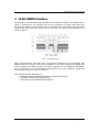
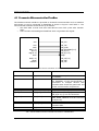
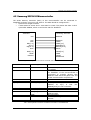
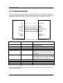
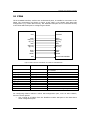
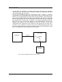
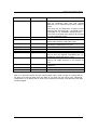
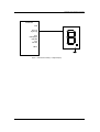
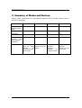
Application Note 2
ZestETM1 User Interface
Examples
Author
Charles Sweeney and Matt Bowen
Version
1.00
Date
16th December 2013
Orange Tree Technologies
Version
1.00
Date
16/12/13
Comment
First version
Disclaimer
This document is intended to provide a note for discussion on various issues and whilst
every effort has been made by Orange Tree Technologies Limited who retain the
ownership thereof to ensure the accuracy of the same, neither these notes or any oral
representations made by any member of Orange Tree Technologies Limited, its servants
or agents, are intended to be relied upon, nor will Orange Tree Technologies Limited, its
employees, members, servants or agents be responsible for any inaccuracies,
infringements of intellectual property rights or any matters of a similar nature arising as a
result of any publication. The information contained herein is not intended to be or
capable of being acted upon or relied upon by third parties and no liability will attach to
Orange Tree Technologies by such use
Page 2 of 18
CONFIDENTIAL
ZestETM1 User Interface Examples
1 References
[1]
ZestETM1 User Guide, Orange Tree Technologies
[2]
MCF532x ColdFire Microprocessor Data Sheet, Freescale Semiconductor
[3]
S3C2416 16/32-Bit RISC Microprocessor User's Manual, Samsung Electronics
[4]
TMS320C645x DSP External Memory Interface (EMIF) User's Guide, Texas
Instruments
CONFIDENTIAL
Page 3 of 18
Orange Tree Technologies
2 Introduction
ZestETM1 is a Gigabit Ethernet interface module and fits between an Ethernet jack and a
local device that can then transfer data to or from the network via ZestETM1. The local
device can be intelligent like a microprocessor or an FPGA, or it can be a non-intelligent
like an ADC.
ZestETM1 has a user interface for connecting to the device, and this user interface can be
configured in a variety of modes to suit the device. This application note describes these
modes and gives examples of how they can be used.
Note that these examples are derived from information in the relevant component
datasheets and have been characterised by design. The designer should check the
relevant datasheet timings for the interface clock frequency that can be achieved.
3 User Interface Modes
The ZestETM1 user interface can be configured in one of four modes:
• 16-bit SRAM interface
• 8-bit SRAM interface
• FIFO interface
• Direct or "bit-banging" interface
Some examples are now given of how to connect devices using each of these modes.
Detailed information about each mode is in the ZestETM1 User Guide [1].
The modes are summarised in the last section at the end of the document.
Page 4 of 18
CONFIDENTIAL
ZestETM1 User Interface Examples
4 16-Bit SRAM Interface
The data bus is 16-bits bidirectional. ZestETM1 is the slave on the bus. The master device
needs a synchronous bus interface that can be configured to access ZBT (Zero Bus
Turnaround) SRAM. The main features of this interface are a single clock cycle chip select
followed two clock cycles later by the read or write data. The basic access waveforms are
shown in Figure 1.
Figure 1. 16-Bit SRAM Interface
Some microcontrollers and DSPs have synchronous interfaces but not specifically ZBT
SRAM interfaces. However it may still be possible to use these interfaces by adding wait
states to position the data correctly, and using a signal such as an address valid strobe
for the chip select. The microcontrollers featured here have such interfaces, please see
the following sections for how to use them.
The example devices described are:
• Freescale microcontrollers with FlexBus external interface [2]
• Samsung S3C2416 microcontroller [3]
• Texas Instruments TMS320C645x DSP [4]
CONFIDENTIAL
Page 5 of 18
Orange Tree Technologies
4.1 Freescale Microcontroller FlexBus
The FlexBus external interface is provided on Freescale microcontrollers such as ColdFire
and Kinetis. It can be connected to ZestETM1 as shown in Figure 2 and Table 1. The
microcontroller interface should be set up as follows:
• One wait state so that write and read data are two clock cycles after Transfer
Start.
• Auto Transfer Acknowledge as ZestETM1 does not generate this signal.
ZestETM1
FlexBus
CLK
FB_CLK
CSn
WEn
BEn[1:0]
A[9:1]
DQ[15:0]
INTn
FB_TSn
FB_R/Wn
FB_BEn/BWEn[1:0]
FB_A[9:1]
FB_D[15:0]
IRQn
EOF[1:0]
HEAD
LENGTH
FB_CS[5:0]
FB_OEn
FB_TAn
Figure 2. Freescale FlexBus Connections to ZestETM1 User Interface in 16-Bit SRAM Mode
ZestETM1
FlexBus
CLK
FB_CLK
CSn
FB_TSn
WEn
BEn[1:0]
A[9:1]
FB_R/Wn
FB_BEn/BWEn[1:0]
FB_A[9:1]
DQ[15:0]
FB_D[15:0]
INTn
IRQn
FB_CS[5:0]
FB_OEn
FB_TAn
Comment
FB_CLK frequency should be from 5MHz
to 125MHz
Transfer Start is used as the Chip Select
for ZestETM1. If the microcontroller is
connected to multiple devices then
Transfer Start should be gated with one
of the microcontroller Chip Selects.
FB_BEn/BWEn [3:2] are not connected
Byte addresses so A[0] is tied low and
FB_A[23:10, 0] are not connected.
FB_D[31:16] are not connected.
EOF, HEAD, LENGTH could be connected
to D[19:16].
Not connected, but see comment for
Transfer Start
Not connected
Not connected
Table 1. Freescale FlexBus Connections to ZestETM1 User Interface in 16-Bit SRAM Mode
Page 6 of 18
CONFIDENTIAL
ZestETM1 User Interface Examples
4.2 Samsung S3C2416 Microcontroller
The Static Memory Controller (SMC) of this microcontroller can be connected to
ZestETM1 as shown in Figure 3 and Table 2. The SMC should be configured for:
• Synchronous single accesses.
• 2 wait states for writes and 1 wait state for reads. This places the data 2 clock
cycles after SMAVD, which is used as the CSn for ZestETM1.
ZestETM1
Samsung S3C2416
CLK
RSMCLK
CSn
WEn
BEn[1:0]
A[9:1]
DQ[15:0]
INTn
RSMAVD
nRWE
nRBE[1:0]
RADDR[8:0]
RDATA[15:0]
EINTn
EOF[1:0]
HEAD
LENGTH
nRCS[5:0]
nROE
nWAIT
RSMBWAIT
Figure 3. Samsung S3C2416 Connections to ZestETM1 User Interface in 16-Bit SRAM Mode
ZestETM1
Samsung S3C2416
CLK
RSMCLK
CSn
RSMAVD
WEn
BEn[1:0]
A[9:1]
nRWE
nRBE[1:0]
RADDR[8:0]
DQ[15:0]
INTn
RDATA[15:0]
EINTn
nRCS[5:0]
nROE
nWAIT
RSMBWAIT
Comment
RSMCLK frequency should be from 5MHz
to 125MHz
Address Valid is used as the Chip Select
for ZestETM1. If the microcontroller is
connected to multiple devices then
Address Valid should be gated with one
of the microcontroller Chip Selects.
A is byte address and RADDR is word
address
so
A[0]
is
tied
low.
RADDR[25:9] are not connected.
Not connected, but see comment for
Address Valid
Not connected
Not used, tie high if not used for other
devices
Not connected
Table 2. Samsung S3C2416 Connections to ZestETM1 User Interface in 16-Bit SRAM Mode
CONFIDENTIAL
Page 7 of 18
Orange Tree Technologies
4.3 TI TMS320C645x DSP
The Texas Instruments TMS320C645x DSP has an external memory interface (EMIF) that
can be configured for Zero Bus Turnaround (ZBT) SRAM. This is suitable for use with the
ZestETM1 16-bit SRAM interface. The connections are shown in Figure 4 and Table 3.
ZestETM1
TMS320C645x
CLK
ECLKOUT
CSn
WEn
BEn[1:0]
A[9:1]
DQ[15:0]
INTn
CEn
SWEn
BEn[1:0]
EA[7:0], BA[1]
ED[15:0]
GPINTn
EOF[1:0]
HEAD
LENGTH
SOEn
SADSn/SREn
BA[0]
Figure 4. TI TMS320C645x Connections to ZestETM1 User Interface in 16-Bit SRAM Mode
ZestETM1
TMS320C645x
CLK
ECLKOUT
CSn
WEn
BEn[1:0]
A[9:1]
CEn
SWEn
BEn[1:0]
EA[7:0], BA[1]
DQ[15:0]
ED[15:0]
INTn
GPINTn
SOEn
SADSn/SREn
BA[1:0]
Comment
ECLKOUT frequency should
5MHz to 125MHz
Any of CEn[5:2] can be used
be
from
BEn[7:2] are not connected
A is byte address and EA is 32-bit word
address so A[0] is tied low and A[1] is
connected to BA[1]. EA[19:8] are not
connected.
ED[63:16] are not connected.
EOF, HEAD, LENGTH could be connected
to ED[19:16] if a 32bit data bus were
used, and then A[9:1]<-EA[8:0].
Not connected
Not connected
Not connected
Table 3. TI TMS320C645x Connections to ZestETM1 User Interface in 16-Bit SRAM Mode
Note that although this DSP has a 10/100/1000 interface of its own, using ZestETM1 has
the following advantages:
Page 8 of 18
CONFIDENTIAL
ZestETM1 User Interface Examples
•
•
•
•
Fast time to market
Reduced project risk
Offload TCP/IP processing burden from the DSP
Very high sustained bandwidth
CONFIDENTIAL
Page 9 of 18
Orange Tree Technologies
5 8-Bit SRAM Interface
This is actually composed of two separate and independent synchronous 8-bit interfaces,
one for writing to ZestETM1 and one for reading from ZestETM1. In both cases ZestETM1
is the slave. Write data is coincident with address and control, but read data has a
latency of 2 clock cycles. See Figure 5 for the waveforms.
Figure 5. 8-Bit SRAM Write and Read Interfaces
Page 10 of 18
CONFIDENTIAL
ZestETM1 User Interface Examples
5.1 FPGA
The 8-bit SRAM interface, with its two unidirectional ports, is suitable for connection to an
FPGA. The connections are shown in Figure 6 and Table 4. For FPGA's with Slave SPI
configuration (e.g. Lattice ECP3 series), the ZestETM1 SPI port can be connected directly
to the FPGA Slave SPI port for configuring the FPGA.
ZestETM1
FPGA
CLK
CLKOUT
WEn
DA[9:0]
D[7:0]
REn
QA[9:0]
Q[7:0]
WEn
QA[9:0]
Q[7:0]
REn
DA[9:0]
D[7:0]
INTn
EOF
HEAD
INTn
EOF
HEAD
SPI
SLAVE SPI CONFIG
Figure 6. FPGA Connections to ZestETM1 User Interface in 8-Bit SRAM Mode
ZestETM1
FPGA
Comment
CLK
CLKOUT
CLKOUT frequency should be from 5MHz
to 125MHz
WEn
DA[9:0]
D[7:0]
REn
QA[9:0]
Q[7:0]
INTn
EOF
HEAD
SPI
WEn
QA[9:0]
Q[7:0]
REn
DA[9:0]
D[7:0]
INTn
EOF
HEAD
SLAVE SPI CONFIG
Write address
Write data
Read address
Read data
Optional SPI for configuring FPGA
Table 4. FPGA Connections to ZestETM1 User Interface in 8-Bit SRAM Mode
For configuring FPGA's without a Slave SPI configuration port, such as Xilinx FPGA's,
there are some options:
• Use a CPLD as a bridge from the ZestETM1 master SPI port to the FPGA slave
serial configuration port.
CONFIDENTIAL
Page 11 of 18
Orange Tree Technologies
•
•
Use SPI flash for configuring the FPGA, and program this flash from ZestETM1
master SPI. There will need to be a multiplexor between the FPGA SPI chip select
and the ZestETM1 SPI chip select.
Use the Xilinx MultiBoot master SPI configuration mode. A "golden" or "fallback"
configuration file is programmed into the SPI flash either by using JTAG via the
FPGA or by pre-programming the flash before board assembly. This configuration
file provides a bridge inside the FPGA from the ZestETM1 user interface to the SPI
flash for programming the "main" configuration file over Ethernet (e.g. using FIFO
high speed mode or master SPI), see Figure 7. The FPGA reconfigures itself from
flash with the main file using the IPROG (internal PROGRAM_B) command and
registers that specify the start address of the file in flash. If the main
configuration also contains the user interface to SPI bridge then the main file in
the flash can be updated in the field. This has the added advantage that if the
main file update fails then the Multiboot fallback feature means that FPGA will fall
back to the golden file and the board can be recovered.
User FPGA
ZestETM1
User I/F
Bridge
SPI Flash
Figure 7. Using the Xilinx Multiboot Scheme to Program an FPGA
Page 12 of 18
CONFIDENTIAL
ZestETM1 User Interface Examples
6 FIFO Interface
Similarly to the 8-bit SRAM mode, this mode has two separate and independent 8-bit
ports, one for data received from Ethernet and one for data to be transmitted to
Ethernet.
Note that this mode is for data transfer only and the ZestETM1 control registers must be
accessed either via the SPI slave interface or the UART interface. If the FIFO interface is
connected to a non-intelligent device such as a DAC or ADC then either a simple
microcontroller can be used for the control registers, or ZestETM1's Auto Connection
facility can be used. With Auto Connection, the control registers do not need to be
accessed as ZestETM1 handles all state control for the Ethernet communication channels.
Figure 8 shows the FIFO waveforms for TCP transfers. Note that UDP transfers add the
datagram length and UDP header to received data, and require datagram length for
transmitted data. Hence UDP transfers can be used only when connected to a device that
can handle these fields, while TCP transfers can be used with non-intelligent devices such
as DAC's and ADC's.
Figure 8. FIFO interface read and write operations for TCP frames
CONFIDENTIAL
Page 13 of 18
Orange Tree Technologies
6.1 DAC and ADC
When using DAC's and ADC's the Ethernet network bandwidth must be greater than the
DAC or ADC data rate in order to ensure one byte per clock cycle to the DAC and from
the ADC. Although ZestETM1 has 1MByte of buffer for each Ethernet transmit channel
and about the same for each Ethernet receive channel, it may be necessary to add buffer
memory between ZestETM1 and the DAC or ADC to ensure a smooth data rate of one
byte per clock cycle. This will depend on the amount of other network traffic interrupting
the ZestETM1 network traffic. If the network is point-to-point between host computer and
ZestETM1 then the ZestETM1 buffers may be adequate.
Figure 9 and Table 5 show a simple scheme without any extra buffering.
Clock
ZestETM1
CLK
Q[7:0]
RXn
RFn[0]
RFn[7:1]
RC[2:0]
DAC
CLK
D[7:0]
'1'
'0'
ADC
CLK
D[7:0]
TXn
TFn[7:0]
TC[2:0]
Q[7:0]
'0'
'0'
INTn
Figure 9. DAC and ADC Connections to ZestETM1 User Interface in FIFO Mode
Page 14 of 18
CONFIDENTIAL
ZestETM1 User Interface Examples
ZestETM1
DAC/ADC
CLK
CLK
Q[7:0]
RXn
D[7:0]
RFn[7:0]
RC[2:0]
D[7:0]
TXn
TFn[7:0]
TC[2:0]
INTn
Q[7:0]
Comment
ZestETM1 clock output is 125MHz, which is too
fast for sustained data rate over gigabit
Ethernet, so an external clock source must be
used.
The clock can be gated with a signal to start
and stop the ADC and DAC - the signal can be
controlled by e.g. ZestETM1 master SPI port.
The clock to the ADC may need to be inverted
to meet ZestETM1 timing.
Data to DAC
Receive strobe optionally connected if the DAC
has a write strobe or chip select input
Receive Full flags - if using GigEx channel 0,
tie RFn[0] high and RFn[7:1] low
Receive channel not connected
Data from ADC
Transmit strobe is not output by ADC's so tie
low or drive by flip-flop controlled from e.g.
ZestETM1 master SPI port or TFn0
Transmit Full flags not connected or connect
TFn[0] (for GigEx channel 0) via inverter to
TXn
Transmit channel tied low to select GigEx
channel 0
Not connected
Table 5. DAC and ADC Connections to ZestETM1 User Interface in FIFO Mode
Note. It is assumed above that the network data rate is high enough for writing data to
the DAC and receiving data from the ADC at one byte per CLK clock cycle. Otherwise,
invalid data (or no data if RXn is used) will be written to the DAC, and data from the ADC
will be dropped.
CONFIDENTIAL
Page 15 of 18
Orange Tree Technologies
7 Direct Interface
The direct or "bit-banging" interface enables 32 pins of the user interface to be set as
either inputs or outputs in groups of 8 pins. These inputs and outputs can then be read or
written by a client on the Ethernet network. The states of outputs are held between
writes so they can be used to generate waveforms controlling devices. There are strobes
and FIFO flags for situations where flow control is required. Only TCP can be used as it
doesn't require header information on the user interface, which UDP does require.
Note that this mode is for data transfer only and the ZestETM1 control registers must be
accessed either via the SPI slave interface or the UART interface. Either a simple
microcontroller can be used for the control registers, or ZestETM1's Auto Connection
facility can be used. With Auto Connection, the control registers do not need to be
accessed as ZestETM1 handles all state control for the Ethernet communication channels.
Figure 10 shows the direct interface without any flow control.
Figure 10. Direct Interface with No Flow Control
This mode can be used to control devices with non-standard interfaces. Some pins could
be data and other pins could be strobes and clocks whose state could be changed on
every cycle of CLK.
For example Figure 11 shows connection to a 7-segment display. It requires simply 8
user interface pins connected to the display's 7 segment pins and 1 decimal point pin.
The CLK is not used by the display but since there must be a user interface clock it is the
125MHz internal clock. The display is updated whenever the device on the network writes
to the GigEx channel 0, which is the only channel that can be connected to the direct
interface. The state of the B outputs is preserved between writes.
Page 16 of 18
CONFIDENTIAL
ZestETM1 User Interface Examples
ZestETM1
CLK
B[7:0]
B[31:8]
Rxn
RxEmptyn
RxFulln
Txn
TxFulln
INTn
Figure 11. Direct Mode Controlling a 7-Segment Display
CONFIDENTIAL
Page 17 of 18
Orange Tree Technologies
8 Summary of Modes and Devices
Table 6 below summarises the recommended mode to use to connect various types of
devices to ZestETM1.
16-Bit SRAM
Microcontroller
Microprocessor
DSP
FPGA
8-Bit SRAM
FIFO
Direct
Yes
Yes
Yes
Yes
Yes
Yes
ADC/DAC
Miscellaneous
devices
with
non-standard
interfaces
Comments
Yes
Bidirectional
bus so more
suited
to
microcontroller
than FPGA
Unidirectional
buses suited to
FPGA
Multiple
Ethernet
channels
available
for
multiple devices
Table 6. Summary of Modes and Devices
Page 18 of 18
CONFIDENTIAL
Only
one
Ethernet
channel so only
one device