1
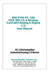
MSI-P710 PC/104 ZigBee
Wireless Card with Analog
In & Digital I/O
User Manual (Preliminary)
PC/104 Embedded
Industrial Analog I/O Series
Microcomputer Systems, Inc.
1814 Ryder Drive ¨ Baton Rouge, LA 70808
Ph (225) 769-2154 ¨ Fax (225) 769-2155
Email: [email protected]
http://www.microcomputersystems.com
MSI-P710 User Manual
Page
CONTENTS
I. INTRODUCTION
1
II.HARDWARE DESCRIPTION
3
A. Card Configuration
B. Card Addressing
3
4
C. Interrupt Connections
D. ZigBee Digital I/O
5
5
ZigBee TTL I/O lines DIO0 thru DIO5
ZigBee TTL input line DI8
Digital I/O connections for J1
E. ZigBee Analog I/O
7
ZigBee analog inputs AIN0 thru AIN5
ZigBee analog outputs AOUT0 and AOUT1
Analog I/O connections for J2
F. UART Digital I/O
9
G. Sleep Mode Configuration
9
III. XBee Pro Wireless Module
10
IV. SAMPLE BASIC LANGUAGE TEST PROGRAM
11
V. SPECIFICATIONS
16
APPENDIX
Schematic Diagrams of the MSI-P710
MSI-P710 User Manual
18
Page
I. INTRODUCTION
The MSI-P710 is a low cost, high performance wireless card
providing the ZigBee protocol using a XBee ZB or XBee-PRO ZB
modules operating at an rf frequency of 2.4 GHz. With advanced
mesh networking functionality, XBee and XBee-PRO ZB modules
improve data traffic management and allow for greater node density.
The card is configurable for Transparent or API operation. Uses
simple AT commands with a standard COM port provided by an
onboard UART. The card can function as a Coordinator, a Router
or an End Device in the ZigBee mesh topology.
A 16C550 UART interfaces the XBee module to the PC/104 bus.
The UART provides a 16 byte transmit and receive FIFO and baud
rates are programmable from 1200 to 115,200 bits/s. Automatic
hardware RTS and CTS flow control is used to prevent overflow of
the local receiver and remote receiver FIFOs. The card I/O address
is jumper selectable for COM1 thru COM4 with an optional 16-bit
offset address. Ten interrupts are jumper selectable for ranges
contained in IRQ2 thru IRQ15. The ZigBee I/O provides 4 lines of
analog inputs individually selectable for 0-5V, 0-10V or 0-20mA
with 10-bit resolution, and 5 TTL selectable as input or output. A
fused [email protected] is provided on the I/O connector is available for
PC/104 16-BIT STACKTHROUGH
CONNECTOR
ADDRESS
JUMPERS
XBEE PRO
MODULE
& ANTENNA
PC/104
BUS
INTERFA C E
NETWORK
PC/104
BUS
INTERRUPT
NETWORK
UART 1
ZigBee DATA
& I/O
Selectable I/O as
Analog In (4) &
Digital I/O (5).
INTERRUPT
JUMPERS
Figure 1. Block Diagram of the MSI-P710.
MSI-P710 User Manual
BLOCK DIAGRAM
Page 1
powering analog and digital sensors connected to the card. All I/O
lines have varistor surge suppressors for transient voltage (lightning,
etc.) protection.
The antenna connection to the card is provided by a SMA bulkhead
connector. A 6" cable attaches this connector to the rf module which
permits its removal from the card bracket for mounting into the user
enclosure as an option. A sample BASIC test program is supplied
that illustrates programming of the card for various XBee PRO
commands. A BASIC interpreter for running this program is available
at no charge.
Operates from -40° to 85° C and requires only +5V.
MSI-P710 User Manual
Page 2
II. HARDWARE DESCRIPTION
A. Card Configuration
The MSI-P710 card is a CMOS design using through-hole and
surface-mounted devices. The card configuration is shown in
Figure 2 and a circuit diagram of the network is given in Appendix
B. The card contains an IBM PC compatible 16C550 UART (U4) that
communicates with a XBee ZB 2.4 GHz rf module that provides the
ZigBee mesh protocol wireless communications. Connector J1
provides for the ZigBee analog in and digital I/O connections. J2 is
a RPSMA bulkhead connector for the antenna connection.
Jumper block JP1 is used for address selection and JP2 for
interrupt configuration, as described below.
Figure 2. MSI-P710 card outline.
MSI-P710 User Manual
Page 3
B. Card Addressing
The card address is set by installing appropriate jumpers on JP1,
pin pairs 1 thru 8, as shown in Fig. 3. An installed jumper for a given
address bit sets the bit to 1 (true) and an uninstalled jumper sets
the bit equal to 0 (false).
Addresses A15 thru A10 (JP1-1 thru JP1-6) are jumper selectable
for defining the base address of the card from 0000H to FC00H on
integral 3FFH boundaries, where H denotes a hexadecimal number.
Addresses A8 and A4 (pins JP1-7 and P1-8) permit assigning
addresses of COM1 thru COM4, as given in Table 1 for a base
address of 0000H.
Table 1. Jumper Selections for COM1 thru COM4.
_____________________________________________________________________
Address** JP1-7 (A8)
JP1-8 (A4)
JP1-1 thru 6 (A15A10)
___________________________________________________________________
COM1
ON
ON
OFF
COM2
OFF
ON
OFF
COM3
ON
OFF
OFF
COM4
OFF
OFF
OFF
_________________________________________________________________
** COM1 = 3F8H, COM2 = 2F8H, COM3 = 3E8H, COM4 = 2E8H.
The base address shown is 0000H (JP1-1 thru JP6 are OFF.
Base addresses selected by installing jumpers on JP1-1 thru JP16 are added to the COMx addresses of Table 1.
Example 1. Set a base address of 8000H for COM1.
A15
A14
A13
A12
A11
A10
A8
A4
o
o
o
o
o
o
o
o
o
o
o
o
o
o
o
o
1
2
3
4
5
6
7
8
JP1
JP1-1, JP1-7 and JP1-8 are ON. All others are OFF. The absolute
address is 8000H + 3F8H = 83F8H.
Figure 3. Jumper block JP1 address configuration.
MSI-P710 User Manual
Page 4
Example 2. Set a base address of 3800H for COM3.
JP1-3, JP1-4, JP1-5 and JP1-7 are ON. All others are OFF. The
absolute address is 3800H + 3E8H = 3BE8H.
C. Interrupt Connections
Interrupt connections are implemented by jumpers JP2-1 thru
JP2-10 as shown in Fig. 4. Jumper selections for selecting
interrupts is given in Table 2. The interrupt is enabled by installing
a jumper on the desired IRQ. JP2-11 provides a 1K pull-down
resistor if it is not provided by the processor card being used.
Table 2. Jumper Selection for Hardware Interrupts.
_____________________________________________________________________
Interrupt** Intall Jumper
Interrupt**
Intall Jumper
___________________________________________________________________
IRQ2(9)
JP2-1
IRQ10
JP2-6
IRQ7
JP2-2
IRQ11
JP2-7
IRQ5
JP2-3
IRQ12
JP2-8
IRQ4
JP2-4
IRQ14
JP2-9
IRQ3
JP2-5
IRQ15
JP2-10
_________________________________________________________________
** Install JP2-11 for 1 KOhm pull-down resistor.
D. ZigBee Digital I/O
The card provides 5 TTL I/O lines that are provided on J1, as given
in Table 4. Individual lines are selected for input or output using
JP3. No installed jumper for a given I/O line sets the line as an input.
Conversely, an installed jumper sets the line as an output, as
11
10
9
8
7
6
o
o
o
o
o
o
o
o
o
o
o
o
o
o
o
o
o
o
o
o
o
o
1
2
3
4
5
JP2
shown in Table 3.
Figure 4. Jumper block JP2 interrupt configuration.
MSI-P710 User Manual
Page 5
Table 3. Jumper Positions for JP3 for Output Selection.
_____________________________________________________________________
Digital Line
Req’d. Jumper
Digital Line
Req’d. Jumper
_____________________________________________________________________
DIO10
JP4-1
DIO4
JP4-4
DIO11
JP4-2
DIO5
JP4-5
DIO12
JP4-3
___________________________________________________________________
Note: No jumper installed sets the digital line for input.
Table 4 gives the digital I/O connections for J1. Even pins (10 thru
18) are connected to digital ground and are signal returns for the
digital I/O of the odd numbered pins 9 thru 17.
Table 4. Digital I/O Pin Connections for J1.
_____________________________________________________________________
Digital Line
J1 Pin No.
Digital Line
J1 Pin No.
_____________________________________________________________________
DIO10
9
DIO4
15
DIO11
11
DIO5
17
DIO12
13
___________________________________________________________________
E. ZigBee Analog Inputs.
The card provides up to 4 analog inputs that are provided on J1,
as given in Table 5. The inputs and outputs are 10-bit with jumper
selectable ranges of 0 to 5V, 0 to 10V and 0 to 20 mA. Input ranges
are selected using JP4, JP5 and JP6, as shown in Table 5.
Table 5. Analog Input Range Selection Required Jumpers.
____________________________________________________________
Range
AIN0
AIN1
AIN2
AIN3
____________________________________________________________
0-5V
JP4-1
JP4-2
JP5-1
JP5-2
0-10V
NONE
NONE
NONE
NONE
0-20mA
JP4-1
JP4-1
JP5-1
JP5-2
JP6-1
JP6-2
JP6-3
JP6-4
____________________________________________________________
MSI-P710 User Manual
Page 6
Table 6 gives the analog input connections for J1. Even pins (2 thru
8) are connected to analog ground and are signal returns for the
analog inputs of the odd numbered pins 1 thru 7.
Table 6. Analog Input Pin Connections for J1.
_____________________________________________________________________
Digital Line
J1 Pin No.
Digital Line
J1 Pin No.
_____________________________________________________________________
AIN0
1
AIN3
5
AIN1
3
AIN4
7
___________________________________________________________________
MSI-P710 User Manual
Page 7
III. XBee Pro Wireless Module
A. Description
The XBee ZB OEM RF Modules were engineered to meet the ZigBee
mesh protocol standards and support the unique needs of lowcost, low-power wireless sensor networks. The modules require
minimal power and provide reliable delivery of data between
devices. The modules operate within the ISM 2.4 GHz frequency
band. The modules have worldwide acceptance as follows:
FCC Approval (USA) Systems that contain XBee-PRO RF Modules
inherit MaxStream Certifications.
ISM (Industrial, Scientific & Medical) 2.4 GHz frequency band.
Manufactured under ISO 9001:2000 registered standards.
XBee ZB RF Modules are optimized for use in the United States,
Canada, Australia, Israel and Europe.
The XBee ZB module is a versatile wireless-to-serial interface
unit that offers over 75 AT commands for configuring the XBee
Pro rf unit and processing data that is transmitted and received
between the module and the PC/104 bus of the MSI-P710.
Details for programming of the rf unit and commands for
exchanging wirelees data is given in the document
XBee ZB Manual.pdf
which is included on this CDROM.
Additional information and up-to-date firmware upgrades can be
viewed at the XBee Pro manufacturers web site at
http://www.digi.com
MSI-P710 User Manual
Page 8
IV. SAMPLE BASIC LANGUAGE TEST PROGRAM
The BASIC language program below illustrates software sequences
for
a. Selecting a COMx port , x = 1, 2, 3 or 4.
b. Setting BAUD rates of 4800 or 9600.
c. Accessing UART digital I/O ports.
d. Sending AT commands.
e. Enabling a receiving mode for displaying of rf data.
f. Use of the API data command.
The program can be run under DOS using a BASIC interpreter
such as QBASIC by Microsoft Corporation. An interpreter can be
provided at no charge upon request.
‘Terminal program for MSI-P710 with UART port at 9600 BAUD (default mode)
COM01 = &H3F8: COM02 = &H2F8: COM3 = &H3E8: COM4 = &H2E8
primary = COM01 ‘set default for primary port (U4) to COM1
‘using jumpers for JP1-7 & JP1-8.
ComDisplay$ = “COM1”
BRATE% = 9600 ‘Default BAUD rate.
CLS
PRINT “”
PRINT “Default address is “; ComDisplay$
PRINT “Address jumper JP2-7 should be installed.”
PRINT “”: PRINT “Strike any key to continue!”
WHILE INKEY$ = “”: WEND
GOSUB init
begin:
CLS
PRINT “”: PRINT “COM Port = “; ComDisplay$, “BAUD Rate = “; BRATE%
PRINT “”
PRINT “(1) Set COMx (x = 1, 2, 3, 4) port.”
PRINT “(2) Set BAUD Rate (4800 or 9600).”
PRINT “(3) Display digital inputs (J3) /IN0 thru /IN2.”
PRINT “(4) Set digital outputs (J3) /OUT0 and /OUT1.”
PRINT “(5) Enter an AT Command (AT prefix not required).”
PRINT “(6) Enable receiving mode (echoes remote data on screen).”
PRINT “(7) Sends HELLO to remote using API 0x08 identifier.”
PRINT “(12) Exit program”
PRINT “”
INPUT “Enter selection - “, GP$
CLS
SELECT CASE GP$
CASE “1” ‘Set COMx port
CLS
MSI-P710 User Manual
Page 9
PRINT “”: PRINT “Present port = “; ComDisplay$
INPUT “Enter COM port # (1, 2, 3, or 4) = “, x
SELECT CASE x
CASE 1
primary = COM01: ComDisplay$ = “COM1”
CASE 2
primary = COM02: ComDisplay$ = “COM2”
CASE 3
primary = COM3: ComDisplay$ = “COM3”
CASE 4
primary = COM4: ComDisplay$ = “COM4”
CASE ELSE
primary = COM01: ComDisplay$ = “COM1”
END SELECT
GOSUB init
CASE “2” ‘Set BAUD Rate
CLS : PRINT “”: PRINT “Present BAUD Rate = “; BRATE%
INPUT “Enter New BAUD Rate (4800 0r 9600) = “, BNEW%
PRINT “”
PRINT “If you have not set the BAUD of the XBee unit to “
PRINT “this BAUD rate, you should use the AT BD command “
PRINT “before you change to this BAUD rate.”
PRINT “”
INPUT “Do you want to change to this BAUD rate? (Y or N) “, q$
IF NOT (q$ = “Y” OR q$ = “y”) THEN GOTO start
IF BNEW% <> 9600 AND BNEW% <> 4800 THEN GOTO start
BRATE% = BNEW%
GOSUB init
CASE “3” ‘Get digital inputs
GOSUB getDInputs
CASE “4”
CLS : PRINT “”
INPUT “DOUT0 (0 or 1) = “, DOUT0%: DOUT0% = DOUT0% * 4
INPUT “DOUT1 (0 or 1) = “, DOUT1%: DOUT1% = DOUT1% * 8 + DOUT0%
outbyte% = INP(primary + 4) OR &HC
outbyte% = NOT DOUT1% AND outbyte%
OUT primary + 4, outbyte%
CASE “5” ‘Enter Command Mode & send command
nextAT:
pchar$ = “”: PRINT “”
INPUT “Enter AT Command (w/o AT) = “, Cstring$
Cstring$ = “AT” + Cstring$
FOR i = 1 TO 3
outchar$ = “+”: GOSUB sendchar
NEXT i
DO
GOSUB getchar
LOOP WHILE pchar$ <> “K”
DO
GOSUB getchar
LOOP WHILE inchar <> 13
GOSUB sendstring ‘send string and await echo
Cstring$ = “ATCN”
GOSUB sendstring ‘send string and await echo
MSI-P710 User Manual
Page 10
PRINT “”: PRINT “Enter Esc key to go to Main Menu.”
DO
x$ = INKEY$
LOOP WHILE x$ = “”
IF CHR$(27) <> x$ THEN GOTO nextAT
CASE “6” ‘Display received characters
DO
GOSUB getchar1
LOOP WHILE INKEY$ = “”
WHILE INKEY$ = “”: WEND ‘Delay for screen freeze
CASE “7” ‘send hello to remote
CLS
outchar = &H7E: GOSUB sendchar1
outchar = 0: GOSUB sendchar1
outchar = 10: GOSUB sendchar1
achk = &HFF
outchar = 1: GOSUB sendchar1
outchar = 44: GOSUB sendchar1
outchar = &H12: GOSUB sendchar1
outchar = &H34: GOSUB sendchar1
outchar = 1: GOSUB sendchar1
outchar = ASC(“H”): GOSUB sendchar1
outchar = ASC(“E”): GOSUB sendchar1
outchar = ASC(“L”): GOSUB sendchar1
outchar = ASC(“L”): GOSUB sendchar1
outchar = ASC(“O”): GOSUB sendchar1
achk = achk AND &HFF
outchar = achk: GOSUB sendchar1
DO
GOSUB getchar1
LOOP WHILE INKEY$ = “”
CASE “12”
END
END SELECT
start:
CLS
GOTO begin
sendstring: ‘send command string
pchar$ = “”: count = 0
FOR i = 1 TO LEN(Cstring$)
outchar$ = MID$(Cstring$, i, 1)
IF outchar$ = “ “ THEN outchar$ = “,”: count = count + 1
GOSUB sendchar
NEXT i
WHILE (INP(primary + 5) AND &H40) = 0: WEND
OUT primary, 13
‘send RET
WHILE (INP(primary + 5) AND &H40) = 0: WEND
FOR q = 0 TO 10000
GOSUB getchar
NEXT q
RETURN
MSI-P710 User Manual
Page 11
init:
‘init MSI-P700 port of U4
OUT primary + 3, &H80’set DLAB = 1
IF BRATE% = 9600 THEN div = 12 ELSE div = 24
OUT primary, div: OUT primary + 1, 0
OUT primary + 3, 3
‘8 data, no parity, 1 stop
OUT primary + 2, 7
FOR i = 0 TO 15: x = INP(primary): NEXT i ‘clear receiver buffer
RETURN
sendchar: ‘Send character outchar$ to primary port
WHILE (INP(primary + 5) AND &H40) = 0: WEND
OUT primary, ASC(outchar$)
GOSUB getchar
RETURN
sendchar1: ‘Send character outchar to primary port
WHILE (INP(primary + 5) AND &H40) = 0: WEND
OUT primary, outchar
GOSUB checksum
RETURN
getchar:
IF (INP(primary + 5) AND 1) = 1 THEN
pchar$ = inchar$
inchar = INP(primary)
inchar$ = CHR$(inchar)
PRINT inchar$;
END IF
RETURN
getchar1:
IF (INP(primary + 5) AND 1) = 1 THEN
inchar = INP(primary)
IF inchar = &H7E THEN PRINT “”
PRINT HEX$(inchar); “ “;
‘ GOTO getchar1
END IF
RETURN
setDOutput: ‘set OUT1_BUFFERED (J1) &h55 or &haa
IF z = 1 THEN
‘set OUT1_BUFFERED (J1-1,3) = 0,1
z = INP(primary + 4) ‘get MODEM control register contents
z = z OR 4
‘set corresponding OUT1 bit in z
z = z AND (NOT 8)
OUT primary + 4, z ‘output to Modem control register
z = INP(secondary + 4) ‘get MODEM control register contents
z = z OR 4
‘set corresponding OUT1 bit in z
z = z AND (NOT 8)
OUT secondary + 4, z ‘output to Modem control register
ELSEIF z = 0 THEN
‘set OUT1_BUFFERED (J1-1,3) = 1,0
z = INP(primary + 4) ‘get MODEM control register contents
z = z AND NOT 4
‘reset corresponding OUT1 bit in z
z = z OR 8
MSI-P710 User Manual
Page 12
OUT primary + 4, z ‘output to Modem control register
z = INP(secondary + 4) ‘get MODEM control register contents
z = z AND NOT 4
‘reset corresponding OUT1 bit in z
z = z OR 8
OUT secondary + 4, z ‘output to Modem control register
END IF
RETURN
getDInputs:
‘get digital inputs from /CTS & /DSR of UARTS
z = INP(primary + 6) AND &HE0
‘get DSR, DCD, RI of primary UART
CLS ‘clear screen
PRINT “”: PRINT “Digital Inputs from J1”: PRINT “”
IF ((z AND &H20) / &H20) > 0 THEN q = 0 ELSE q = 1 ‘invert DSR bit
PRINT “/IN0 (J3-10) = “; q
‘display /IN0
IF ((z AND &H80) / &H80) > 0 THEN q = 0 ELSE q = 1 ‘invert DCD bit
PRINT “/IN1 (J3-8) = “; q
‘display /IN1
IF ((z AND &H40) / &H40) > 0 THEN q = 0 ELSE q = 1 ‘invert /RI bit
PRINT “/IN2 (J3-6) = “; q
‘display /IN2
WHILE INKEY$ = “”: WEND ‘delay until keyboard character entry
RETURN
checksum:
achk = achk - outchar
RETURN
MSI-P710 User Manual
Page 13
V. SPECIFICATIONS
PC/104 Bus
16-bit, stackthrough
XBee PRO ZB Module
Indoor/urban Range:
Up to 300’ (90 m).
Outdoor Range:
Up to 1 mile (1.6 km) line-of-sight.
Transmit Power Output:
50 mW (17 dBm)
Int’l. 10mW (10 dBm) EIRP.
Operating Frequency:
2.4 GHz.
RF Data Rate:
250,000 bps.
Receiver Sensitivity:
-102 dBm (1% PER).
ZigBee Analog Inputs:
4 selectable 10-bit channels,
0-5V, 0-10V, 0-20mA ranges.
ZigBee TTL digital I/O:
5 selectable as TTL input or
output.
Serial Port
UART:
I/O Address:
16C550
Jumper selectable as COM1
thru COM4 with an optional
16-bit offset.
Interrupts:
Jumper selectable for IRQ3 thru
IRQ5, IRQ7 and IRQ9 thru
IQ15.
Selectable 1K pull-down resistor
I/O Connectors
3M 30320-5002
Option Jumpers
.025" square posts, 0.1" grid
Electrical & Environmental
+5V @ 70 mA typical, idle/receive mode
+5V @ 205 mA typical, transmit mode (10 dBm)
+5V @ 285 mA typical, transmit mode (18 dBm)
+5V @ 45 mA typical, power save mode
Operating Temperature: -40° to 85° C
MSI-P710 User Manual
Page 14
Ordering Information
MSI-P710
AIO & DIO w/RPSMA bulkhead
MSI-P710-X
Excludes I/O w/RPSMA bulkhead
Accessories
MSI-WiPort-Ant
Omni-directional "Rubber Duck" antenna,
2.4 GHz, 3 dBi, Reverse Polarity SMA.
MSI-P710 User Manual
Page 15
APPENDIX
Schematic Diagrams of the MSI-P710
1) P710-1.sch - Schematic sheet 1 of 3.
See p710-1.pdf
2) P710-2.sch - Schematic sheet 2 of 3.
See p710-2.pdf
3) P710-3.sch - Schematic sheet 3 of 3.
See p710-3.pdf
MSI-P710 User Manual
Page 16