1
Application Note 1330
The USB switches are bi-directional, which allows the host
(computer) and downstream USB device to both send and
receive data.
Full-Speed Switches
The two FSx switches (FSD1, FSD2) are bi-directional
switches that can pass rail-to-rail signals. When powered
with a 3.3V supply, these switches have a nominal rON
resistance of 7Ω over the signal range of 0V to 3.3V. They
were specifically designed to pass USB full-speed (12Mbps)
differential signals and meet the USB 2.0 full-speed signal
quality specifications.
The FSx switches can also pass USB high speed signals
(480Mbps) but do not quite meet the USB 2.0 high speed
signal quality eye diagram compliance requirement.
The maximum signal range for the FSx switches is from
-1.5V to VDD. The signal voltage should not be allowed to
exceed the VDD voltage rail or go below ground by more
than -1.5V.
When operated with a 3.3V to 3.6V supply, the FSx switches
are active (turned ON) whenever the IN logic control voltage
is ≤0.5V and the EN logic voltage is ≥1.4V.
High-Speed Switches
The two HSx switches (HSD2, HSD1) are bi-directional
switches that can pass rail-to-rail signals. When powered
with a 3.3V supply, these switches have a nominal rON of
4.5Ω over the signal range of 0V to 400mV with a rON
flatness of 0.4Ω. The rON matching between the HSD1 and
HSD2 switches over this signal range is only 0.01Ω ensuring
minimal impact by the switches to USB high speed signal
transitions. As the signal level increases, the rON switch
resistance increases. At signal level of 3.3V the switch
resistance is nominally 20Ω.
3
The HSx switches were specifically designed to pass USB
2.0 high-speed (480Mbps) differential signals typically in the
range of 0V to 400mV. They have low capacitance and high
bandwidth to pass the USB high-speed signals with
minimum edge and phase distortion to meet USB 2.0 high
speed signal quality specifications.
The HSx switches can also pass USB full-speed signals
(12Mbps) with minimal distortion and meet all the USB
requirements for USB 2.0 full-speed signaling.
The maximum signal range for the HSx switches is from
-1.5V to VDD. The signal voltage should not exceed the VDD
voltage rail or go below ground by more than -1.5V.
The HSx switches are active (turned ON) whenever the IN
voltage is ≥1.4V and the EN logic voltage ≥1.4V when
operated with a 3.3V to 3.6V supply.
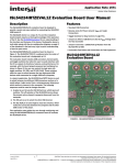
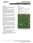
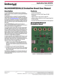
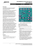
Board Component Definitions
DESIGNATOR
DESCRIPTION
U1
ISL54200IRUZ IC
J1
“B” type USB Receptacle
J2, J3
“A” type USB Receptacle
J4
VDD Positive Connection
J5
VDD Negative Connection
J6
IN Logic Control
J7
EN Logic Control
J8
VBUS Voltage for Highspeed Device
J9
VBUS Voltage for Fullspeed Device
JP1, JP2, JP3 D-/D+ Differential Probe Connection
JP4, JP5
Host Controller VBUS Jumper
AN1330.0
June 13, 2007