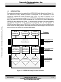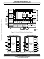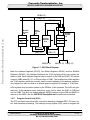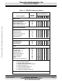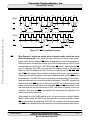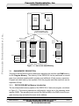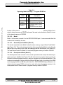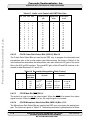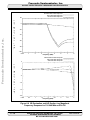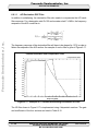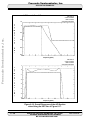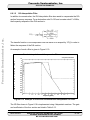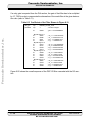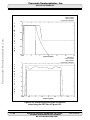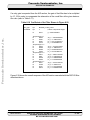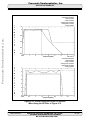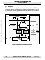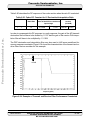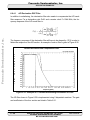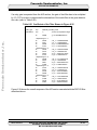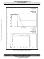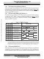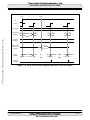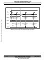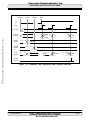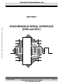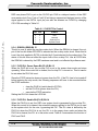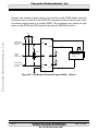
1
Freescale Semiconductor, Inc. TABLE OF CONTENTS Freescale Semiconductor, Inc... Paragraph Number Title Page Number SECTION 1 DSP56156 OVERVIEW 1.1 1.2 1.2.1 1.2.2 1.2.3 1.2.4 1.2.5 1.2.5.1 1.2.5.2 1.2.5.3 1.3 1.4 1.4.1 1.4.2 1.4.3 1.4.4 1.4.5 1.5 1.6 1.6.1 1.6.1.1 1.6.1.2 1.6.2 1.6.2.1 1.6.2.2 1.6.2.3 1.6.3 1.6.3.1 INTRODUCTION . . . . . . . . . . . . . . . . . . . . . . . . . . . . . . . . . . . . . . . . . . DSP56100 CORE BLOCK DIAGRAM DESCRIPTION . . . . . . . . . . . . . Data Buses . . . . . . . . . . . . . . . . . . . . . . . . . . . . . . . . . . . . . . . . . . . . Address Buses . . . . . . . . . . . . . . . . . . . . . . . . . . . . . . . . . . . . . . . . . Data ALU . . . . . . . . . . . . . . . . . . . . . . . . . . . . . . . . . . . . . . . . . . . . . Address Generation Unit (AGU) . . . . . . . . . . . . . . . . . . . . . . . . . . . . Program Control Unit (PCU) . . . . . . . . . . . . . . . . . . . . . . . . . . . . . . . Interrupt Priority Structure . . . . . . . . . . . . . . . . . . . . . . . . . . . . . . Interrupt Priority Levels (IPL) . . . . . . . . . . . . . . . . . . . . . . . . . . . Exception Priorities within an IPL . . . . . . . . . . . . . . . . . . . . . . . . MEMORY ORGANIZATION . . . . . . . . . . . . . . . . . . . . . . . . . . . . . . . . . EXTERNAL BUS, I/O, AND ON-CHIP PERIPHERALS . . . . . . . . . . . . . Memory Expansion Port (Port A) . . . . . . . . . . . . . . . . . . . . . . . . . . . General Purpose I/O (Port B, Port C) . . . . . . . . . . . . . . . . . . . . . . . . SSI0 and SSI1 . . . . . . . . . . . . . . . . . . . . . . . . . . . . . . . . . . . . . . . . . Timer . . . . . . . . . . . . . . . . . . . . . . . . . . . . . . . . . . . . . . . . . . . . . . . . Host Interface (HI) . . . . . . . . . . . . . . . . . . . . . . . . . . . . . . . . . . . . . . OnCE . . . . . . . . . . . . . . . . . . . . . . . . . . . . . . . . . . . . . . . . . . . . . . . . . . . PROGRAMMING MODEL . . . . . . . . . . . . . . . . . . . . . . . . . . . . . . . . . . . Data ALU . . . . . . . . . . . . . . . . . . . . . . . . . . . . . . . . . . . . . . . . . . . . . Data ALU Input Registers (X1, X0, Y1, Y0) . . . . . . . . . . . . . . . . Data ALU Accumulator Registers (A2, A1, A0, B2, B1, B0) . . . . Address Generation Unit . . . . . . . . . . . . . . . . . . . . . . . . . . . . . . . . . Address Register File (R0-R3) . . . . . . . . . . . . . . . . . . . . . . . . . . Offset Register File (N0-N3) . . . . . . . . . . . . . . . . . . . . . . . . . . . . Modifier Register File (M0-M3) . . . . . . . . . . . . . . . . . . . . . . . . . . Program Control Unit . . . . . . . . . . . . . . . . . . . . . . . . . . . . . . . . . . . . Program Counter (PC) . . . . . . . . . . . . . . . . . . . . . . . . . . . . . . . . MOTOROLA TABLE OF CONTENTS For More Information On This Product, Go to: www.freescale.com 1-3 1-5 1-7 1-7 1-8 1-9 1-10 1-12 1-12 1-12 1-12 1-12 1-16 1-16 1-16 1-17 1-17 1-18 1-18 1-18 1-18 1-19 1-19 1-19 1-19 1-21 1-21 1-21 i Freescale Semiconductor, Inc. Table of Contents (Continued) Freescale Semiconductor, Inc... Paragraph Number 1.6.3.2 1.6.3.3 1.6.3.4 1.6.3.5 1.6.3.6 1.6.3.7 1.7 1.7.1 1.7.1.1 1.7.1.2 1.7.1.3 1.7.1.4 1.7.1.5 1.7.1.6 1.7.2 1.7.3 1.7.4 1.7.4.1 1.7.4.2 1.7.4.3 Title Page Number Status Register (SR) . . . . . . . . . . . . . . . . . . . . . . . . . . . . . . . . . . Loop Counter (LC) . . . . . . . . . . . . . . . . . . . . . . . . . . . . . . . . . . . Loop Address Register (LA) . . . . . . . . . . . . . . . . . . . . . . . . . . . . System Stack (SS) . . . . . . . . . . . . . . . . . . . . . . . . . . . . . . . . . . . Stack Pointer (SP) . . . . . . . . . . . . . . . . . . . . . . . . . . . . . . . . . . . Operating Mode Register (OMR) . . . . . . . . . . . . . . . . . . . . . . . . INSTRUCTION SET SUMMARY . . . . . . . . . . . . . . . . . . . . . . . . . . . . . . Instruction Groups . . . . . . . . . . . . . . . . . . . . . . . . . . . . . . . . . . . . . . Arithmetic Instructions . . . . . . . . . . . . . . . . . . . . . . . . . . . . . . . . . Logical Instructions . . . . . . . . . . . . . . . . . . . . . . . . . . . . . . . . . . . Bit Field Manipulation Instructions . . . . . . . . . . . . . . . . . . . . . . . Loop Instructions . . . . . . . . . . . . . . . . . . . . . . . . . . . . . . . . . . . . . Move Instructions . . . . . . . . . . . . . . . . . . . . . . . . . . . . . . . . . . . . Program Control Instructions . . . . . . . . . . . . . . . . . . . . . . . . . . . Instruction Formats . . . . . . . . . . . . . . . . . . . . . . . . . . . . . . . . . . . . . . Addressing Modes . . . . . . . . . . . . . . . . . . . . . . . . . . . . . . . . . . . . . . Address Arithmetic . . . . . . . . . . . . . . . . . . . . . . . . . . . . . . . . . . . . . . Linear Modifier . . . . . . . . . . . . . . . . . . . . . . . . . . . . . . . . . . . . . . Reverse Carry Modifier . . . . . . . . . . . . . . . . . . . . . . . . . . . . . . . Modulo Modifier . . . . . . . . . . . . . . . . . . . . . . . . . . . . . . . . . . . . . 1-21 1-22 1-23 1-23 1-23 1-24 1-26 1-26 1-27 1-28 1-29 1-29 1-29 1-30 1-30 1-31 1-33 1-33 1-33 1-34 SECTION 2 DSP56156 PIN DESCRIPTIONS 2.1 2.2 2.3 2.4 2.5 2.6 2.7 2.8 2.9 2.10 ii INTRODUCTION . . . . . . . . . . . . . . . . . . . . . . . . . . . . . . . . . . . . . . . . . . ADDRESS AND DATA BUS (32 PINS) . . . . . . . . . . . . . . . . . . . . . . . . . BUS CONTROL (9 PINS) . . . . . . . . . . . . . . . . . . . . . . . . . . . . . . . . . . . INTERRUPT AND MODE CONTROL (3 PINS) . . . . . . . . . . . . . . . . . . POWER, GROUND, AND CLOCK (28 PINS) . . . . . . . . . . . . . . . . . . . . HOST INTERFACE (15 PINS) . . . . . . . . . . . . . . . . . . . . . . . . . . . . . . . . 16-BIT TIMER (2 PINS) . . . . . . . . . . . . . . . . . . . . . . . . . . . . . . . . . . . . . SYNCHRONOUS SERIAL INTERFACES (SSI0 AND SSI1) (10 PINS) ON-CHIP EMULATION (4 PINS) . . . . . . . . . . . . . . . . . . . . . . . . . . . . . . ON-CHIP CODEC (7 PINS) . . . . . . . . . . . . . . . . . . . . . . . . . . . . . . . . . . TABLE OF CONTENTS For More Information On This Product, Go to: www.freescale.com 2-3 2-3 2-3 2-9 2-10 2-11 2-12 2-12 2-13 2-14 MOTOROLA Freescale Semiconductor, Inc. Table of Contents (Continued) Paragraph Number Title Page Number Freescale Semiconductor, Inc... SECTION 3 OPERATING MODES AND MEMORY SPACES 3.1 RAM MEMORY DESCRIPTION . . . . . . . . . . . . . . . . . . . . . . . . . . . . . . 3.1.1 DSP56156 RAM Part Memory Introduction . . . . . . . . . . . . . . . . . . . 3.1.1.1 X Data Memory . . . . . . . . . . . . . . . . . . . . . . . . . . . . . . . . . . . . . . 3.1.1.2 Program Memory . . . . . . . . . . . . . . . . . . . . . . . . . . . . . . . . . . . . 3.1.1.3 Bootstrap Memory . . . . . . . . . . . . . . . . . . . . . . . . . . . . . . . . . . . . 3.1.1.4 Chip Operating Modes . . . . . . . . . . . . . . . . . . . . . . . . . . . . . . . . 3.1.1.4.1 Bootstrap Mode (Mode 0) . . . . . . . . . . . . . . . . . . . . . . . . . . . 3.1.1.4.2 Bootstrap Mode (Mode 1) . . . . . . . . . . . . . . . . . . . . . . . . . . . 3.1.1.4.3 Normal Expanded Mode (Mode 2) . . . . . . . . . . . . . . . . . . . . 3.1.1.4.4 Development Mode (Mode 3) . . . . . . . . . . . . . . . . . . . . . . . . 3.1.2 Bootstrap Mode . . . . . . . . . . . . . . . . . . . . . . . . . . . . . . . . . . . . . . . . 3.1.2.1 Bootstrap ROM . . . . . . . . . . . . . . . . . . . . . . . . . . . . . . . . . . . . . . 3.1.2.2 Bootstrap Control Logic . . . . . . . . . . . . . . . . . . . . . . . . . . . . . . . 3.1.2.3 Bootstrap Program . . . . . . . . . . . . . . . . . . . . . . . . . . . . . . . . . . . 3.2 ROM MEMORY DESCRIPTION . . . . . . . . . . . . . . . . . . . . . . . . . . . . . . 3.2.1 DSP56156 ROM Part Memory Introduction . . . . . . . . . . . . . . . . . . . 3.2.1.1 X Data Memory . . . . . . . . . . . . . . . . . . . . . . . . . . . . . . . . . . . . . . 3.2.1.2 Program Memory . . . . . . . . . . . . . . . . . . . . . . . . . . . . . . . . . . . . 3.2.1.3 Chip Operating Modes . . . . . . . . . . . . . . . . . . . . . . . . . . . . . . . . 3.2.1.3.1 Single-chip Mode (Mode 0) . . . . . . . . . . . . . . . . . . . . . . . . . . 3.2.1.3.2 Mode 1 . . . . . . . . . . . . . . . . . . . . . . . . . . . . . . . . . . . . . . . . . . 3.2.1.3.3 Normal Expanded Mode (Mode 2) . . . . . . . . . . . . . . . . . . . . 3.2.1.3.4 Development Mode (Mode 3) . . . . . . . . . . . . . . . . . . . . . . . . MOTOROLA TABLE OF CONTENTS For More Information On This Product, Go to: www.freescale.com 3-3 3-3 3-4 3-4 3-4 3-5 3-5 3-6 3-6 3-6 3-6 3-6 3-7 3-7 3-9 3-9 3-10 3-10 3-10 3-10 3-11 3-11 3-11 iii Freescale Semiconductor, Inc. Table of Contents (Continued) Paragraph Number Title Page Number Freescale Semiconductor, Inc... SECTION 4 I/O INTERFACE 4.1 4.2 4.2.1 4.2.1.1 4.2.1.2 INTRODUCTION . . . . . . . . . . . . . . . . . . . . . . . . . . . . . . . . . . . . . . . . . . I/O PORT SET-UP AND PROGRAMMING . . . . . . . . . . . . . . . . . . . . . . Port Registers . . . . . . . . . . . . . . . . . . . . . . . . . . . . . . . . . . . . . . . . . . Bus Control Register (BCR) . . . . . . . . . . . . . . . . . . . . . . . . . . . . Port B and Port C registers . . . . . . . . . . . . . . . . . . . . . . . . . . . . . 4-3 4-3 4-4 4-4 4-6 SECTION 5 HOST INTERFACE 5.1 5.2 5.3 5.4 5.5 5.6 5.7 5.7.1 5.7.2 5.7.3 5.8 5.8.1 5.8.2 5.8.3 5.8.4 5.8.5 5.8.6 5.9 5.9.1 5.9.2 5.9.3 5.9.4 5.9.5 iv INTRODUCTION . . . . . . . . . . . . . . . . . . . . . . . . . . . . . . . . . . . . . . . . . . HOST INTERFACE PROGRAMMING MODEL . . . . . . . . . . . . . . . . . . . HOST TRANSMIT DATA REGISTER (HTX) . . . . . . . . . . . . . . . . . . . . . RECEIVE BYTE REGISTERS (RXH, RXL) . . . . . . . . . . . . . . . . . . . . . . TRANSMIT BYTE REGISTERS (TXH, TXL) . . . . . . . . . . . . . . . . . . . . . HOST RECEIVE DATA REGISTER (HRX) . . . . . . . . . . . . . . . . . . . . . . COMMAND VECTOR REGISTER (CVR) . . . . . . . . . . . . . . . . . . . . . . . CVR Host Vector (HV) Bits 0 through 4 . . . . . . . . . . . . . . . . . . . . . . CVR Reserved bits – Bits 5 and 6 . . . . . . . . . . . . . . . . . . . . . . . . . . CVR Host Command Bit (HC) Bit 7 . . . . . . . . . . . . . . . . . . . . . . . . . HOST CONTROL REGISTER (HCR) . . . . . . . . . . . . . . . . . . . . . . . . . . HCR Host Receive Interrupt Enable (HRIE) Bit 0 . . . . . . . . . . . . . . HCR Host Transmit Interrupt Enable (HTIE) Bit 1 . . . . . . . . . . . . . . HCR Host Command Interrupt Enable (HCIE) Bit 2 . . . . . . . . . . . . . HCR Host Flag 2 (HF2) Bit 3 . . . . . . . . . . . . . . . . . . . . . . . . . . . . . . HCR Host Flag 3 (HF3) Bit 4 . . . . . . . . . . . . . . . . . . . . . . . . . . . . . . HCR Reserved Control – Bits 5, 6 and 7 . . . . . . . . . . . . . . . . . . . . . HOST STATUS REGISTER (HSR) . . . . . . . . . . . . . . . . . . . . . . . . . . . . HSR Host Receive Data Full (HRDF) Bit 0 . . . . . . . . . . . . . . . . . . . HSR Host Transmit Data Empty (HTDE) Bit 1 . . . . . . . . . . . . . . . . . HSR Host Command Pending (HCP) Bit 2 . . . . . . . . . . . . . . . . . . . HSR Host Flag 0 (HF0) Bit 3 . . . . . . . . . . . . . . . . . . . . . . . . . . . . . . HSR Host Flag 1 (HF1) Bit 4 . . . . . . . . . . . . . . . . . . . . . . . . . . . . . . TABLE OF CONTENTS For More Information On This Product, Go to: www.freescale.com 5-3 5-5 5-5 5-5 5-5 5-6 5-7 5-7 5-7 5-9 5-9 5-10 5-10 5-10 5-10 5-10 5-11 5-11 5-11 5-11 5-11 5-12 5-12 MOTOROLA Freescale Semiconductor, Inc. Table of Contents (Continued) Freescale Semiconductor, Inc... Paragraph Number 5.9.6 5.9.7 5.10 5.10.1 5.10.2 5.10.3 5.10.4 5.10.5 5.10.6 5.10.7 5.11 5.11.1 5.11.2 5.11.3 5.11.4 5.11.5 5.11.6 5.11.7 5.11.8 5.12 5.13 5.14 5.14.1 5.14.2 5.14.3 5.14.4 5.15 5.15.1 5.15.2 Title Page Number HSR Reserved Status – Bits 5 and 6 . . . . . . . . . . . . . . . . . . . . . . . . HSR DMA Status (DMA) Bit 7 . . . . . . . . . . . . . . . . . . . . . . . . . . . . . INTERRUPT CONTROL REGISTER (ICR) . . . . . . . . . . . . . . . . . . . . . . ICR Receive Request Enable (RREQ) Bit 0 . . . . . . . . . . . . . . . . . . . ICR Transmit Request Enable (TREQ) Bit 1 . . . . . . . . . . . . . . . . . . ICR Reserved bit – Bit 2 . . . . . . . . . . . . . . . . . . . . . . . . . . . . . . . . . . ICR Host Flag 0 (HF0) Bit 3 . . . . . . . . . . . . . . . . . . . . . . . . . . . . . . . ICR Host Flag 1 (HF1) Bit 4 . . . . . . . . . . . . . . . . . . . . . . . . . . . . . . . ICR Host Mode Control (HM1, HM0) Bits 5 and 6 . . . . . . . . . . . . . . ICR Initialize Bit (INIT) Bit 7 . . . . . . . . . . . . . . . . . . . . . . . . . . . . . . . INTERRUPT STATUS REGISTER (ISR) . . . . . . . . . . . . . . . . . . . . . . . ISR Receive Data Register Full (RXDF) Bit 0 . . . . . . . . . . . . . . . . . ISR Transmit Data Register Empty (TXDE) Bit 1 . . . . . . . . . . . . . . . ISR Transmitter Ready (TRDY) Bit 2 . . . . . . . . . . . . . . . . . . . . . . . . ISR Host Flag 2 (HF2) Bit 3 . . . . . . . . . . . . . . . . . . . . . . . . . . . . . . . ISR Host Flag 3 (HF3) Bit 4 . . . . . . . . . . . . . . . . . . . . . . . . . . . . . . . ISR (Reserved Status) Bit 5 . . . . . . . . . . . . . . . . . . . . . . . . . . . . . . . ISR DMA Status (DMA) Bit 6 . . . . . . . . . . . . . . . . . . . . . . . . . . . . . . ISR Host Request (HREQ) Bit 7 . . . . . . . . . . . . . . . . . . . . . . . . . . . . INTERRUPT VECTOR REGISTER (IVR) . . . . . . . . . . . . . . . . . . . . . . . IVR HOST INTERFACE INTERRUPTS . . . . . . . . . . . . . . . . . . . . . . . . DMA MODE OPERATION . . . . . . . . . . . . . . . . . . . . . . . . . . . . . . . . . . . Host to DSP – Host Interface Action . . . . . . . . . . . . . . . . . . . . . . . . Host To DSP – Host Processor Procedure . . . . . . . . . . . . . . . . . . . DSP to Host Interface Action . . . . . . . . . . . . . . . . . . . . . . . . . . . . . . DSP To Host – Host Processor Procedure . . . . . . . . . . . . . . . . . . . HOST PORT USAGE – GENERAL CONSIDERATIONS . . . . . . . . . . . Host Programmer Considerations . . . . . . . . . . . . . . . . . . . . . . . . . . DSP programmer considerations . . . . . . . . . . . . . . . . . . . . . . . . . . . 5-12 5-12 5-12 5-12 5-13 5-13 5-13 5-14 5-14 5-15 5-16 5-16 5-16 5-16 5-17 5-17 5-17 5-17 5-17 5-17 5-18 5-18 5-19 5-19 5-20 5-21 5-21 5-21 5-23 SECTION 6 MOTOROLA TABLE OF CONTENTS For More Information On This Product, Go to: www.freescale.com v Freescale Semiconductor, Inc. Table of Contents (Continued) Paragraph Number Title Page Number Freescale Semiconductor, Inc... DSP56156 ON-CHIP SIGMA/DELTA CODEC 6.1 6.2 6.3 6.4 6.4.1 6.4.2 6.4.3 6.4.4 6.4.5 6.4.5.1 6.4.5.2 6.4.5.3 6.4.5.4 6.4.5.5 6.4.5.6 6.4.5.7 6.4.5.8 6.4.6 6.4.6.1 6.4.6.2 6.4.6.3 6.4.6.4 6.4.6.5 6.5 6.5.1 6.5.2 6.5.2.1 6.5.2.2 6.5.2.3 6.5.2.4 6.6 6.6.1 6.6.1.1 vi INTRODUCTION . . . . . . . . . . . . . . . . . . . . . . . . . . . . . . . . . . . . . . . . . . GENERAL DESCRIPTION . . . . . . . . . . . . . . . . . . . . . . . . . . . . . . . . . . ANALOG I/O DEFINITION . . . . . . . . . . . . . . . . . . . . . . . . . . . . . . . . . . . INTERFACE WITH THE DSP56156 CORE PROCESSOR . . . . . . . . . Interface Definition . . . . . . . . . . . . . . . . . . . . . . . . . . . . . . . . . . . . . . On-chip Codec Programming Model . . . . . . . . . . . . . . . . . . . . . . . . Codec Receive Register (CRX) . . . . . . . . . . . . . . . . . . . . . . . . . . . . Codec Transmit Register (CTX) . . . . . . . . . . . . . . . . . . . . . . . . . . . . Codec Control Register (COCR) . . . . . . . . . . . . . . . . . . . . . . . . . . . COCR Audio Level Control Bits (VC3-VC0) Bits 0-3 . . . . . . . . . COCR Codec Ratio Select Bits (CRS1-0) Bits 8,9 . . . . . . . . . . . COCR Mute Bit (MUT) Bit 10 . . . . . . . . . . . . . . . . . . . . . . . . . . . COCR Microphone Gain Select Bits (MGS1-0) Bits 11,12 . . . . . COCR Input Select Bit (INS) Bit 13 . . . . . . . . . . . . . . . . . . . . . . . COCR Codec Enable Bit (COE) Bit 14 . . . . . . . . . . . . . . . . . . . . COCR Codec Interrupt Enable Bit (COIE) Bit 15 . . . . . . . . . . . . COCR Reserved Bits (Bits 4-7) . . . . . . . . . . . . . . . . . . . . . . . . . Codec Status Register (COSR) . . . . . . . . . . . . . . . . . . . . . . . . . . . . COSR Codec Transmit Under Run Error FLag Bit (CTUE) Bit 0 COSR Codec Receive Overrun Error Flag Bit (CROE) Bit 1 . . . COSR Codec Transmit Data Empty Bit (CTDE) Bit 2 . . . . . . . . . COSR Codec Receive Data Full Bit (CRDF) Bit 3 . . . . . . . . . . . COSR Reserved Bits (Bits 4-15) . . . . . . . . . . . . . . . . . . . . . . . . . ON-CHIP CODEC FREQUENCY RESPONSE AND GAIN ANALYSIS A/D Section Frequency Response and DC Gain . . . . . . . . . . . . . . . D/A Section Frequency Response and DC Gain . . . . . . . . . . . . . . . D/A Second Order Digital Comb Filter . . . . . . . . . . . . . . . . . . . . D/A Analog Comb Decimating Filter . . . . . . . . . . . . . . . . . . . . . . D/A Analog Low Pass Filter . . . . . . . . . . . . . . . . . . . . . . . . . . . . D/A Section Overall Frequency Response . . . . . . . . . . . . . . . . . APPLICATION EXAMPLES . . . . . . . . . . . . . . . . . . . . . . . . . . . . . . . . . . Example 1 . . . . . . . . . . . . . . . . . . . . . . . . . . . . . . . . . . . . . . . . . . . . A/D Decimation DSP Filter . . . . . . . . . . . . . . . . . . . . . . . . . . . . . TABLE OF CONTENTS For More Information On This Product, Go to: www.freescale.com 6-3 6-3 6-4 6-5 6-5 6-6 6-6 6-6 6-7 6-7 6-8 6-8 6-8 6-9 6-9 6-9 6-9 6-9 6-9 6-10 6-10 6-10 6-10 6-12 6-12 6-17 6-19 6-21 6-24 6-26 6-30 6-30 6-32 MOTOROLA Freescale Semiconductor, Inc. Table of Contents (Continued) Freescale Semiconductor, Inc... Paragraph Number 6.6.1.2 6.6.2 6.6.2.1 6.6.2.2 6.6.3 6.6.3.1 6.6.3.2 6.6.4 6.6.4.1 6.6.4.2 6.6.5 6.7 Title Page Number D/A Interpolation Filter . . . . . . . . . . . . . . . . . . . . . . . . . . . . . . . . 6-35 Example 2 . . . . . . . . . . . . . . . . . . . . . . . . . . . . . . . . . . . . . . . . . . . . 6-38 A/D Decimation DSP Filter . . . . . . . . . . . . . . . . . . . . . . . . . . . . . 6-40 D/A Interpolation Filter . . . . . . . . . . . . . . . . . . . . . . . . . . . . . . . . 6-43 Example 3 . . . . . . . . . . . . . . . . . . . . . . . . . . . . . . . . . . . . . . . . . . . . 6-46 A/D Decimation DSP Filter . . . . . . . . . . . . . . . . . . . . . . . . . . . . . 6-48 D/A Interpolation Filter . . . . . . . . . . . . . . . . . . . . . . . . . . . . . . . . 6-51 Example 4 . . . . . . . . . . . . . . . . . . . . . . . . . . . . . . . . . . . . . . . . . . . . 6-54 A/D Decimation DSP Filter . . . . . . . . . . . . . . . . . . . . . . . . . . . . . 6-56 D/A Interpolation Filter . . . . . . . . . . . . . . . . . . . . . . . . . . . . . . . . 6-59 Example 5 — Real-Time I/O Example with On-Chip Codec and PLL 6-62 DSP PROGRAM FLOWCHART . . . . . . . . . . . . . . . . . . . . . . . . . . . . . . 6-65 SECTION 7 16-BIT TIMER AND EVENT COUNTER 7.1 7.2 7.3 7.4 7.5 7.6 7.6.1 7.6.2 7.6.3 7.6.4 7.6.5 7.6.6 7.6.7 7.7 7.8 INTRODUCTION . . . . . . . . . . . . . . . . . . . . . . . . . . . . . . . . . . . . . . . . . . TIMER ARCHITECTURE . . . . . . . . . . . . . . . . . . . . . . . . . . . . . . . . . . . TIMER COUNT REGISTER (TCTR) . . . . . . . . . . . . . . . . . . . . . . . . . . . TIMER PRELOAD REGISTER (TPR) . . . . . . . . . . . . . . . . . . . . . . . . . . TIMER COMPARE REGISTER (TCPR) . . . . . . . . . . . . . . . . . . . . . . . . TIMER CONTROL REGISTER (TCR) . . . . . . . . . . . . . . . . . . . . . . . . . . TCR Decrement Ratio (DC7-DC0) Bit 0-7 . . . . . . . . . . . . . . . . . . . . TCR Event Select (ES) Bit 8 . . . . . . . . . . . . . . . . . . . . . . . . . . . . . . TCR Overflow Interrupt Enable (OIE) Bit 9 . . . . . . . . . . . . . . . . . . . TCR Compare Interrupt Enable (CIE) Bit 10 . . . . . . . . . . . . . . . . . . TCR Timer Output Enable (TO2-TO0) Bit 11-13 . . . . . . . . . . . . . . . TCR Inverter Bit (INV) Bit 14 . . . . . . . . . . . . . . . . . . . . . . . . . . . . . . TCR Timer Enable (TE) Bit 15 . . . . . . . . . . . . . . . . . . . . . . . . . . . . . TIMER RESOLUTION . . . . . . . . . . . . . . . . . . . . . . . . . . . . . . . . . . . . . . FUNCTIONAL DESCRIPTION OF THE TIMER . . . . . . . . . . . . . . . . . . 7-3 7-3 7-3 7-4 7-5 7-6 7-6 7-6 7-6 7-7 7-7 7-7 7-8 7-8 7-8 SECTION 8 MOTOROLA TABLE OF CONTENTS For More Information On This Product, Go to: www.freescale.com vii Freescale Semiconductor, Inc. Table of Contents (Continued) Paragraph Number Page Number Title Freescale Semiconductor, Inc... SYNCHRONOUS SERIAL INTERFACE (SSI0 and SSI1) 8.1 8.2 8.3 8.4 8.4.1 8.4.2 8.4.3 8.4.4 8.4.5 8.5 8.6 8.7 8.8 8.9 8.10 8.11 8.11.1 8.11.2 8.11.3 8.11.4 8.12 8.12.1 8.12.2 8.12.3 8.12.4 8.12.5 8.12.6 8.12.7 8.12.8 8.12.9 8.12.10 8.12.11 viii INTRODUCTION . . . . . . . . . . . . . . . . . . . . . . . . . . . . . . . . . . . . . . . . . . 8-3 SSI OPERATING MODES . . . . . . . . . . . . . . . . . . . . . . . . . . . . . . . . . . . 8-3 SSI CLOCK AND FRAME SYNC GENERATION . . . . . . . . . . . . . . . . . 8-4 SSIx DATA AND CONTROL PINS . . . . . . . . . . . . . . . . . . . . . . . . . . . . 8-4 Serial Transmit Data Pin - STDx . . . . . . . . . . . . . . . . . . . . . . . . . . . 8-7 Serial Receive Data Pin - SRDx . . . . . . . . . . . . . . . . . . . . . . . . . . . . 8-7 Serial Clock - SCK . . . . . . . . . . . . . . . . . . . . . . . . . . . . . . . . . . . . . . 8-7 Serial Control - SC1x . . . . . . . . . . . . . . . . . . . . . . . . . . . . . . . . . . . . 8-7 Serial Control - SC0x . . . . . . . . . . . . . . . . . . . . . . . . . . . . . . . . . . . . 8-8 SSI RESET AND INITIALIZATION PROCEDURE . . . . . . . . . . . . . . . . 8-8 SSIx INTERFACE PROGRAMMING MODEL . . . . . . . . . . . . . . . . . . . . 8-9 SSI TRANSMIT SHIFT REGISTER . . . . . . . . . . . . . . . . . . . . . . . . . . . . 8-10 SSI TRANSMIT DATA REGISTER (TX) . . . . . . . . . . . . . . . . . . . . . . . . 8-12 SSI RECEIVE SHIFT REGISTER . . . . . . . . . . . . . . . . . . . . . . . . . . . . . 8-12 SSI RECEIVE DATA REGISTER (RX) . . . . . . . . . . . . . . . . . . . . . . . . . 8-12 SSI CONTROL REGISTER A (CRA) . . . . . . . . . . . . . . . . . . . . . . . . . . . 8-12 CRA Prescale Modulus Select (PM0…PM7) Bits 0-7 . . . . . . . . . . . 8-13 CRA Frame Rate Divider Control (DC0…DC4) Bits 8-12 . . . . . . . . 8-13 CRA Word Length Control (WL0,WL1) Bits 13, 14 . . . . . . . . . . . . . 8-14 CRA Prescaler Range (PSR) Bit 15 . . . . . . . . . . . . . . . . . . . . . . . . . 8-15 SSI CONTROL REGISTER B (CRB) . . . . . . . . . . . . . . . . . . . . . . . . . . . 8-15 CRB Serial Output Flag 0 and 1 (OF0, OF1) Bit 0, 1 . . . . . . . . . . . . 8-16 Transmit and Receive Frame Sync Directions - (FSD0, FSD1) Bit 2,4 8-16 CRB A/Mu Law Selection Bit (A/MU) Bit 3 . . . . . . . . . . . . . . . . . . . . 8-17 Transmit and Receive Frame Sync Directions - (FSD1) Bit 4 . . . . . 8-17 CRB Clock Source Direction (SCKD) Bit 5 . . . . . . . . . . . . . . . . . . . . 8-17 CRB Clock Polarity Bit (SCKP) Bit 6 . . . . . . . . . . . . . . . . . . . . . . . . 8-17 CRB MSB Position Bit (SHFD) Bit 7 . . . . . . . . . . . . . . . . . . . . . . . . . 8-17 CRB Frame Sync Length (FSL) Bit 8 . . . . . . . . . . . . . . . . . . . . . . . . 8-17 CRB Frame Sync Invert (FSI) Bit 9 . . . . . . . . . . . . . . . . . . . . . . . . . 8-17 CRB Sync/Async (SYN) Bit 10 . . . . . . . . . . . . . . . . . . . . . . . . . . . . . 8-18 CRB SSI Mode Select (MOD) Bit 11 . . . . . . . . . . . . . . . . . . . . . . . . 8-18 TABLE OF CONTENTS For More Information On This Product, Go to: www.freescale.com MOTOROLA Freescale Semiconductor, Inc. Table of Contents (Continued) Freescale Semiconductor, Inc... Paragraph Number 8.12.12 8.12.13 8.12.14 8.12.15 8.13 8.13.1 8.13.2 8.13.3 8.13.4 8.13.5 8.13.6 8.13.7 8.14 8.15 8.16 8.17 8.18 8.19 8.19.1 8.19.1.1 8.19.1.2 8.19.2 8.19.2.1 8.19.2.2 8.19.2.3 Title Page Number CRB SSI Transmit Enable (TE) Bit 12 . . . . . . . . . . . . . . . . . . . . . . . CRB SSI Receive Enable (RE) Bit 13 . . . . . . . . . . . . . . . . . . . . . . . CRB SSI Transmit Interrupt Enable (TIE) Bit 14 . . . . . . . . . . . . . . . CRB SSI Receive Interrupt Enable (RIE) Bit 15 . . . . . . . . . . . . . . . . SSI STATUS REGISTER (SSISR) . . . . . . . . . . . . . . . . . . . . . . . . . . . . SSISR Serial Input Flag 1 and 0 (IF0, IF1) Bit 0, 1 . . . . . . . . . . . . . SSISR Transmit Frame Sync (TFS) Bit 2 . . . . . . . . . . . . . . . . . . . . . SSISR Receive Frame Sync (RFS) Bit 3 . . . . . . . . . . . . . . . . . . . . . SSISR Transmitter Underrun Error (TUE) Bit 4 . . . . . . . . . . . . . . . . SSISR Receiver Overrun Error (ROE) Bit 5 . . . . . . . . . . . . . . . . . . . SSISR Transmit Data Register Empty (TDE) Bit 6 . . . . . . . . . . . . . . SSISR Receive Data Register Full (RDF) Bit 7 . . . . . . . . . . . . . . . . TIME SLOT REGISTER - TSR . . . . . . . . . . . . . . . . . . . . . . . . . . . . . . . TRANSMIT SLOT MASK REGISTERS - TSMAx AND TSMBx . . . . . . . TRANSMIT SLOT MASK SHIFT REGISTER - TSMS . . . . . . . . . . . . . . RECEIVE SLOT MASK REGISTERS - RSMAx AND RSMBx . . . . . . . RECEIVE SLOT MASK SHIFT REGISTER - RSMS . . . . . . . . . . . . . . . SSI OPERATING MODES . . . . . . . . . . . . . . . . . . . . . . . . . . . . . . . . . . . Normal Operating Mode . . . . . . . . . . . . . . . . . . . . . . . . . . . . . . . . . . Normal Mode Transmit . . . . . . . . . . . . . . . . . . . . . . . . . . . . . . . . Normal Mode Receive . . . . . . . . . . . . . . . . . . . . . . . . . . . . . . . . Network Mode . . . . . . . . . . . . . . . . . . . . . . . . . . . . . . . . . . . . . . . . . Network Mode Transmit . . . . . . . . . . . . . . . . . . . . . . . . . . . . . . . Network Mode Receive . . . . . . . . . . . . . . . . . . . . . . . . . . . . . . . . On-Demand Mode . . . . . . . . . . . . . . . . . . . . . . . . . . . . . . . . . . . 8-18 8-18 8-19 8-19 8-19 8-20 8-20 8-20 8-21 8-21 8-21 8-22 8-22 8-22 8-23 8-23 8-24 8-24 8-25 8-25 8-25 8-25 8-26 8-27 8-27 SECTION 9 ON-CHIP FREQUENCY SYNTHESIZER 9.1 9.1.1 9.1.1.1 9.1.1.2 9.1.1.3 9.2 9.2.1 INTRODUCTION . . . . . . . . . . . . . . . . . . . . . . . . . . . . . . . . . . . . . . . . . . PLL Components . . . . . . . . . . . . . . . . . . . . . . . . . . . . . . . . . . . . . . . Phase Comparator and Filter . . . . . . . . . . . . . . . . . . . . . . . . . . . Voltage Controlled Oscillator (VCO) . . . . . . . . . . . . . . . . . . . . . . Dividers . . . . . . . . . . . . . . . . . . . . . . . . . . . . . . . . . . . . . . . . . . . . ON-CHIP CLOCK SYNTHESIS EXAMPLES . . . . . . . . . . . . . . . . . . . . Example One . . . . . . . . . . . . . . . . . . . . . . . . . . . . . . . . . . . . . . . . . . MOTOROLA TABLE OF CONTENTS For More Information On This Product, Go to: www.freescale.com 9-3 9-3 9-3 9-4 9-4 9-5 9-5 ix Freescale Semiconductor, Inc. Table of Contents (Continued) Freescale Semiconductor, Inc... Paragraph Number 9.2.2 9.2.3 9.3 9.3.1 9.3.2 9.3.3 9.3.4 9.3.5 9.3.6 9.3.7 9.3.8 Title Page Number Example Two . . . . . . . . . . . . . . . . . . . . . . . . . . . . . . . . . . . . . . . . . . Example Three . . . . . . . . . . . . . . . . . . . . . . . . . . . . . . . . . . . . . . . . . ON-CHIP CLOCK SYNTHESIS CONTROL REGISTER PLCR . . . . . . PLCR Input Divider Bits (ED3-ED0) Bits 0-3 . . . . . . . . . . . . . . . . . . PLCR Feedback Divider Bits (YD3-YD0) Bits 4-7 . . . . . . . . . . . . . . PLCR Clockout Select Bits (CS1-CS0) Bits 10-11 . . . . . . . . . . . . . . GSM Bit (GSM) Bit 12 . . . . . . . . . . . . . . . . . . . . . . . . . . . . . . . . . . . PLCR PLL Power Down Bit (PLLD) Bit 13 . . . . . . . . . . . . . . . . . . . . PLCR PLL Enable Bit (PLLE) Bit 14 . . . . . . . . . . . . . . . . . . . . . . . . . PLCR Voltage Controlled Oscillator Lock Bit (LOCK) Bit 15 . . . . . . PLCR Reserved Bits (Bits 8-9,12) . . . . . . . . . . . . . . . . . . . . . . . . . . 9-6 9-7 9-7 9-7 9-7 9-7 9-8 9-8 9-8 9-9 9-9 APPENDIX A BOOTSTRAP MODE OPERATING MODE 0 OR 1 A.1 INTRODUCTION. . . . . . . . . . . . . . . . . . . . . . . . . . . . . . . . . . . . . . . . . . . . . .13 A.2 BOOTSTRAP ROM. . . . . . . . . . . . . . . . . . . . . . . . . . . . . . . . . . . . . . . . . . . .13 A.2.1 Bootstrap Control Logic . . . . . . . . . . . . . . . . . . . . . . . . . . . . . . . . . . . . . .13 A.2.2 Bootstrap Firmware Program. . . . . . . . . . . . . . . . . . . . . . . . . . . . . . . . . .14 APPENDIX B DSP56156 APPLICATION EXAMPLES APPENDIX C PROGRAMMING SHEETS C.1 C.2 x PERIPHERAL ADDRESSES . . . . . . . . . . . . . . . . . . . . . . . . . . . . . . . . . . . .27 INSTRUCTIONS . . . . . . . . . . . . . . . . . . . . . . . . . . . . . . . . . . . . . . . . . . . . . .29 TABLE OF CONTENTS For More Information On This Product, Go to: www.freescale.com MOTOROLA Freescale Semiconductor, Inc. Table of Contents (Continued) Freescale Semiconductor, Inc... Paragraph Number C.3 C.4 C.5 C.6 C.7 C.8 C.9 C.10 C.11 Title Page Number CORE . . . . . . . . . . . . . . . . . . . . . . . . . . . . . . . . . . . . . . . . . . . . . . . . . . . . . .42 P.L.L.. . . . . . . . . . . . . . . . . . . . . . . . . . . . . . . . . . . . . . . . . . . . . . . . . . . . . . .45 Timer . . . . . . . . . . . . . . . . . . . . . . . . . . . . . . . . . . . . . . . . . . . . . . . . . . . . . . .47 Timer . . . . . . . . . . . . . . . . . . . . . . . . . . . . . . . . . . . . . . . . . . . . . . . . . . . . . . .48 Codec . . . . . . . . . . . . . . . . . . . . . . . . . . . . . . . . . . . . . . . . . . . . . . . . . . . . . .49 Codec . . . . . . . . . . . . . . . . . . . . . . . . . . . . . . . . . . . . . . . . . . . . . . . . . . . . . .50 GP I/O . . . . . . . . . . . . . . . . . . . . . . . . . . . . . . . . . . . . . . . . . . . . . . . . . . . . . .51 HOST . . . . . . . . . . . . . . . . . . . . . . . . . . . . . . . . . . . . . . . . . . . . . . . . . . . . . .53 SSI . . . . . . . . . . . . . . . . . . . . . . . . . . . . . . . . . . . . . . . . . . . . . . . . . . . . . . . .58 MOTOROLA TABLE OF CONTENTS For More Information On This Product, Go to: www.freescale.com xi Freescale Semiconductor, Inc. Table of Contents (Continued) Title Page Number Freescale Semiconductor, Inc... Paragraph Number xii TABLE OF CONTENTS For More Information On This Product, Go to: www.freescale.com MOTOROLA Freescale Semiconductor, Inc. LIST of FIGURES Figure Number Page Number Title Freescale Semiconductor, Inc... SECTION 1 1-1 1-2 1-3 1-4 1-5 1-6 1-7 1-8 1-9 1-10 1-11 1-12 DSP56100 Family Product Literature . . . . . . . . . . . . Detailed RAM Based Part Block Diagram . . . . . . . . . . Detailed ROM Based Part Block Diagram . . . . . . . . . . DSP56156 RAM and ROM Based Functional Block Diagram DSP56100 CORE Block Diagram . . . . . . . . . . . . . . Data ALU Architecture Block Diagram . . . . . . . . . . . . AGU Block Diagram . . . . . . . . . . . . . . . . . . . . . Interrupt Priority Register IPR (Address X:$FFDF) . . . . . Input/Output Block Diagram . . . . . . . . . . . . . . . . . DSP56156 Programming Model . . . . . . . . . . . . . . . Status Register Format . . . . . . . . . . . . . . . . . . . Operating Mode Register . . . . . . . . . . . . . . . . . . . . . . . . . . . . . . . . . . . . . . . . . . . . . . . . . . . . . . . . . . . . . . . . . . . . . . . . . . . . . . . . . . . . . . . . . . . . . . . . . . . . . . . . . . . . . . . . . . 1-3 1-5 1-6 1-6 1-7 1-9 1-10 1-11 1-14 1-20 1-22 1-25 SECTION 2 2-1 2-2 2-3 Bus Operation . . . . . . . . . . . . . . . . . . . . . . . . . . . . . . . . 2-4 DSP56156 Pinout . . . . . . . . . . . . . . . . . . . . . . . . . . . . . . 2-5 TA Controlled Accesses . . . . . . . . . . . . . . . . . . . . . . . . . . . 2-7 SECTION 3 3-1 3-2 DSP56156 RAM Memory Map . . . . . . . . . . . . . . . . . . . . . . . . 3-3 DSP56156 ROM Memory Map . . . . . . . . . . . . . . . . . . . . . . . 3-9 4-1 4-2 4-3 DSP56156 Input / Output Block Diagram . . . . . . . . . . . . . . . . . . 4-5 I/O Port B and C Programming Models . . . . . . . . . . . . . . . . . . . 4-7 DSP56156 On-chip peripherals Memory Map . . . . . . . . . . . . . . . . 4-8 5-1 5-2 5-3 Host Interface Block Diagram . . . . . . . . . . . . . . . . . . . . . . . . 5-4 Host Interface - DSP Programming Model . . . . . . . . . . . . . . . . . . 5-6 Host Interface - Host Processor Programming Model . . . . . . . . . . . . 5-8 6-1 6-2 6-3 6-4 DSP56156 On-chip Sigma/Delta Functional Diagram . . . . . . . DSP56156 Analog Input and Output Diagram . . . . . . . . . . . On-Chip Codec Programming Model . . . . . . . . . . . . . . . Log Magnitude Frequency Response of the A/D Comb Filter for F=2.048 MHz and D=128 . . . . . . . . . . . Log Magnitude Frequency Response of the A/D Comb Filter in the 0-4 KHz Band for F=2.048 MHz and D=128 SECTION 4 SECTION 5 SECTION 6 6-5 MOTOROLA Revision 2.1 LIST of FIGURES For More Information On This Product, DSP56004 DESIGN SPECIFICATION Go to: www.freescale.com . . . . . 6-3 . . . . . 6-5 . . . . . 6-6 . . . . . 6-13 . . . . . 6-14 xiii xiii Freescale Semiconductor, Inc. List of Figures (Continued) Figure Number 6-6 6-7 6-8 Freescale Semiconductor, Inc... 6-9 6-10 6-11 6-12 6-13 6-14 6-15 6-16 6-17 6-18 6-19 6-20 6-21 6-22 6-23 6-24 6-25 6-26 6-27 6-28 6-29 6-30 6-31 xiv Page Number Title IIR Decimation and A/D Section Log Magnitude Frequency Response for F=2.048 MHz and D=128 . . . . . . . . Log Magnitude Frequency Responses of the Three Sections in the D/A for F=2.048 MHz and D=128 . . . . . . Log Magnitude Frequency Response of the D/A Comb Filter for F=2.048MHz and D=128 . . . . . . . . . . . Log Magnitude Frequency Response of the D/A Analog Comb Filter for F=2.048 MHz . . . . . . . . . . . . . Log Magnitude Frequency Response of the D/A Analog Comb Filter for F=2.048 MHz . . . . . . . . . . . . . Log Magnitude Frequency Response of the D/A Analog Low-pass Filter for F=512 KHz . . . . . . . . . . . . Log Magnitude Frequency Response of the D/A Section for F=2.048 MHz and D=128 . . . . . . . . . . . . . Log Magnitude Frequency Response of the D/A Section for F=2.048 MHz and D=128 . . . . . . . . . . . . . IIR Interpolation and D/A Section Log Magnitude Frequency Response for F=2.048 MHz and D=128 . . . . . . . . Example 1 functional block diagram . . . . . . . . . . . . . . . Example of Transmit and Receive Filter Performance Constraints Example of a Transmit Antialiasing-decimation IIR Filter . . . . . Overall Response of the A/D Section when Using the IIR Filter of Figure 6-17. . . . . . . . . . . . . . Example of a Receive Reconstruction-interpolation IIR Filter . . . Overall Response of the D/A Section When Using the IIR Filter of Figure 6-19 . . . . . . . . . . . . . . Example 2 functional block diagram . . . . . . . . . . . . . . . . Example of Transmit and Receive Filter Performance Constraints Example of a Transmit Antialiasing-decimation IIR Filter . . . . . Overall Response of the A/D Section when Using the IIR Filter of Figure 6-23. . . . . . . . . . . . . . Example of a Receive Reconstruction-interpolation IIR Filter . . . Overall Response of the D/A Section When Using the IIR Filter of Figure 6-25 . . . . . . . . . . . . . . Example 3 functional block diagram . . . . . . . . . . . . . . . . Example of Transmit and Receive Filter Performance Constraints Example of GSM Transmit Antialiasing-decimation IIR Filter . . . Overall Response of the A/D Section when Using the IIR Filter of Figure 6-29. . . . . . . . . . . . . . Example of a Receive Reconstruction-interpolation IIR Filter . . . LIST of FIGURES For More Information On This Product, Go to: www.freescale.com . . . . . 6-16 . . . . . 6-18 . . . . . 6-20 . . . . . 6-22 . . . . . 6-23 . . . . . 6-25 . . . . . 6-26 . . . . . 6-27 . . . . . . . . . . . . . . . . . . . . 6-29 6-30 6-31 6-32 . . . . . 6-34 . . . . . 6-35 . . . . . . . . . . . . . . . . . . . . 6-37 6-38 6-39 6-40 . . . . . 6-42 . . . . . 6-43 . . . . . . . . . . . . . . . . . . . . 6-45 6-46 6-47 6-48 . . . . . 6-50 . . . . . 6-51 MOTOROLA Freescale Semiconductor, Inc. List of Figures (Continued) Figure Number 6-32 Freescale Semiconductor, Inc... 6-33 6-34 6-35 6-36 6-37 6-38 6-39 Page Number Title Overall Response of the D/A Section When Using the IIR Filter of Figure 6-31 . . . . . . . . . . . . . . Example 4 functional block diagram . . . . . . . . . . . . . . . . Example of Transmit and Receive Filter Performance Constraints Example of a Transmit Antialiasing-decimation IIR Filter . . . . . Overall Response of the A/D Section when Using the IIR Filter of Figure 6-35 . . . . . . . . . . . . . . Example of a Receive Reconstruction-interpolation IIR Filter . . . Overall Response of the D/A Section When Using the IIR Filter of Figure 6-37 . . . . . . . . . . . . . . Flowchart of a Decimation/Interpolation Routine . . . . . . . . . . . . . . . . . . . . . . . . . . . . . 6-53 6-54 6-55 6-56 . . . . . 6-58 . . . . . 6-59 . . . . . 6-61 . . . . . 6-67 SECTION 7 7-1 7-2 7-3 7-4 7-5 7-6 16-bit Timer General Block Diagram . . . . . . . . Timer Programming Model . . . . . . . . . . . . . Timer Control Register . . . . . . . . . . . . . . . Standard Timer Operation with Overflow Interrupt . Standard Timer Disable . . . . . . . . . . . . . . . . . . . . . . . . . . . . . . . . . . . . . . . . . . . . . . . . . . . . . . . . . . . . . . . . . . . . . . . . . . . . . . . 7-4 7-5 7-6 7-9 7-9 Write to the Count Register After Writing to the Preload Register when the Timer is Disabled 7-7 Timer Disable After a Write to the Count Register . . . . . . . . 7-8 Write to the Count Register when the Timer is Enabled . . . . . 7-9 Write to DC7-DC0 when the Timer is Enabled . . . . . . . . . . 7-10 Standard Timer Operation with Compare Interrupt . . . . . . . . . . . . . . . . . . . . . . . . . . . . . . . . . . . . . 7-10 7-10 7-11 7-12 7-13 8-1 8-2 8-3 8-4 8-5 8-6 8-7 8-8 8-9 SSIx Internal Clock, Synchronous Operation . . . . . . . . . . . SSIx External Clock, Synchronous Operation . . . . . . . . . . . SSIx Internal Clock, Asynchronous Operation . . . . . . . . . . . SSIx External Clock, Asynchronous Operation . . . . . . . . . . SSIx Internal Clock, Synchronous Operation Dual Codec Interface SSI Clock Generator Functional Block Diagram . . . . . . . . . . SSIx Frame Sync Generator Functional Block Diagram . . . . . . SSIx Programming Model . . . . . . . . . . . . . . . . . . . . . SSI Control Register B . . . . . . . . . . . . . . . . . . . . . . . . . . . . . . . . . . . . . . . . . . . . . . . . . . . . . . . . . . . . . . . . . . . . 8-5 8-5 8-5 8-5 8-6 8-6 8-8 8-10 8-16 9-1 9-2 9-3 A A-1 Frequency Synthesis Block Diagram and Control Register . . . . . . . . . 9-5 Three On-chip Clock Synthesis Examples . . . . . . . . . . . . . . . . . . 9-6 On-chip Frequency Synthesizer Programming Model Summary . . . . . . 9-10 SECTION 8 SECTION 9 DSP56156 Bootstrap Program Listing . . . . . . . . . . . . . . . . . . . . . . . . . . . . . . 15 MOTOROLA LIST of FIGURES For More Information On This Product, Go to: www.freescale.com xv Freescale Semiconductor, Inc. List of Figures (Continued) Freescale Semiconductor, Inc... Figure Number B B-1 B-2 B-3 B-4 B-5 C C-1 C-2 C-3 C-4 C-5 C-6 C-7 C-8 C-9 C-10 C-11 C-12 C-13 C-14 C-15 C-16 C-17 C-18 C-19 C-20 C-21 C-22 C-23 C-24 C-25 C-26 C-27 C-28 C-29 C-30 C-31 C-32 C-33 xvi Title Page Number No Glue Logic, Low Cost Memory Port Bootstrap — Mode 0 . . . . . . . . . . . . DSP56156 Host Bootstrap Example — Mode 1 . . . . . . . . . . . . . . . . . . . . . . 32K Words of External Program ROM — Mode 2 . . . . . . . . . . . . . . . . . . . . . Reset Circuit. . . . . . . . . . . . . . . . . . . . . . . . . . . . . . . . . . . . . . . . . . . . . . . . . . Reset Circuit Using 555 Timer . . . . . . . . . . . . . . . . . . . . . . . . . . . . . . . . . . . . 21 21 22 23 23 On-chip Peripherals Memory Map . . . . . . . . . . . . . . . . . . . . . . . . . . . . . . . . . Bus Control Register (BCR) . . . . . . . . . . . . . . . . . . . . . . . . . . . . . . . . . . . . . . Status Register (SR) . . . . . . . . . . . . . . . . . . . . . . . . . . . . . . . . . . . . . . . . . . . Interrupt Priority Register (IPR) . . . . . . . . . . . . . . . . . . . . . . . . . . . . . . . . . . . Operating Mode Register (OMR) . . . . . . . . . . . . . . . . . . . . . . . . . . . . . . . . . . PLL Control Register (PLCR). . . . . . . . . . . . . . . . . . . . . . . . . . . . . . . . . . . . . On-chip Frequency Synthesizer Programming Model Summary . . . . . . . . . . Timer Control Register (TCR) . . . . . . . . . . . . . . . . . . . . . . . . . . . . . . . . . . . . Timer Count Register (TCTR) . . . . . . . . . . . . . . . . . . . . . . . . . . . . . . . . . . . . Timer Compare Register (TCPR). . . . . . . . . . . . . . . . . . . . . . . . . . . . . . . . . . Timer Preload Register (TPR) . . . . . . . . . . . . . . . . . . . . . . . . . . . . . . . . . . . . Codec Status Register (COSR) . . . . . . . . . . . . . . . . . . . . . . . . . . . . . . . . . . . Transmit Data Register (CTX) . . . . . . . . . . . . . . . . . . . . . . . . . . . . . . . . . . . . Receive Data Register (CRX) . . . . . . . . . . . . . . . . . . . . . . . . . . . . . . . . . . . . Control Register (PBC) . . . . . . . . . . . . . . . . . . . . . . . . . . . . . . . . . . . . . . . . . Data Direction Register (PBDDR) . . . . . . . . . . . . . . . . . . . . . . . . . . . . . . . . . Data Register (PBD) . . . . . . . . . . . . . . . . . . . . . . . . . . . . . . . . . . . . . . . . . . . Control Register (PCC) . . . . . . . . . . . . . . . . . . . . . . . . . . . . . . . . . . . . . . . . . Data Direction Register (PCDDR) . . . . . . . . . . . . . . . . . . . . . . . . . . . . . . . . . Data Register (PCD) . . . . . . . . . . . . . . . . . . . . . . . . . . . . . . . . . . . . . . . . . . . Control Register (PBC) . . . . . . . . . . . . . . . . . . . . . . . . . . . . . . . . . . . . . . . . . Host Control Register (HCR) . . . . . . . . . . . . . . . . . . . . . . . . . . . . . . . . . . . . . Host Transmit Data Register (HTX) . . . . . . . . . . . . . . . . . . . . . . . . . . . . . . . . Host Receive Data Register (HRX) . . . . . . . . . . . . . . . . . . . . . . . . . . . . . . . . Host Status Register (HSR) . . . . . . . . . . . . . . . . . . . . . . . . . . . . . . . . . . . . . . Command Vector Register (CVR) . . . . . . . . . . . . . . . . . . . . . . . . . . . . . . . . . Interrupt Control Register (ICR) . . . . . . . . . . . . . . . . . . . . . . . . . . . . . . . . . . . Interrupt Status Register (ISR). . . . . . . . . . . . . . . . . . . . . . . . . . . . . . . . . . . . Interrupt Vector Register (IVR). . . . . . . . . . . . . . . . . . . . . . . . . . . . . . . . . . . . Receive Byte Registers . . . . . . . . . . . . . . . . . . . . . . . . . . . . . . . . . . . . . . . . . Transmit Byte Registers. . . . . . . . . . . . . . . . . . . . . . . . . . . . . . . . . . . . . . . . . SSI Serial Transmit Register . . . . . . . . . . . . . . . . . . . . . . . . . . . . . . . . . . . . . SSI Serial Receive Register. . . . . . . . . . . . . . . . . . . . . . . . . . . . . . . . . . . . . . 27 42 42 43 44 45 46 47 48 48 48 49 50 50 51 51 51 52 52 52 53 53 54 54 54 55 55 56 57 57 57 58 58 LIST of FIGURES For More Information On This Product, Go to: www.freescale.com MOTOROLA Freescale Semiconductor, Inc. List of Figures (Continued) Freescale Semiconductor, Inc... Figure Number C-34 C-35 C-36 C-37 C-38 C-39 C-40 C-41 Title Page Number SSI Control Register (PCC) . . . . . . . . . . . . . . . . . . . . . . . . . . . . . . . . . . . . . . SSI Receive Slot Mask. . . . . . . . . . . . . . . . . . . . . . . . . . . . . . . . . . . . . . . . . . SSI Receive Slot Mask. . . . . . . . . . . . . . . . . . . . . . . . . . . . . . . . . . . . . . . . . . SSI Transmit Slot Mask . . . . . . . . . . . . . . . . . . . . . . . . . . . . . . . . . . . . . . . . . SSI Transmit Slot Mask . . . . . . . . . . . . . . . . . . . . . . . . . . . . . . . . . . . . . . . . . SSI Control Register A (CRA) . . . . . . . . . . . . . . . . . . . . . . . . . . . . . . . . . . . . SSI Control Register B (CRB) . . . . . . . . . . . . . . . . . . . . . . . . . . . . . . . . . . . . SSI Status Register (SSISR) . . . . . . . . . . . . . . . . . . . . . . . . . . . . . . . . . . . . . MOTOROLA LIST of FIGURES For More Information On This Product, Go to: www.freescale.com 58 59 59 60 60 61 61 62 xvii Freescale Semiconductor, Inc... Freescale Semiconductor, Inc. xviii LIST of FIGURES For More Information On This Product, Go to: www.freescale.com MOTOROLA Freescale Semiconductor, Inc. LIST of TABLES Table Number Title Page Number Freescale Semiconductor, Inc... 1 1-1 1-2 1-3 1-4 1-5 1-6 1-7 1-8 1-9 1-10 1-11 DSP56156 Feature List . . . . . . . . . . . . . . . . . . . . . . . . . . . . . . . . . . . . . . . . Status Register Interrupt Mask Bits . . . . . . . . . . . . . . . . . . . . . . . . . . . . . . . External Interrupt Trigger Mode Bits . . . . . . . . . . . . . . . . . . . . . . . . . . . . . . Interrupt Priority Level Bits . . . . . . . . . . . . . . . . . . . . . . . . . . . . . . . . . . . . . . Exception Priorities within an IPL. . . . . . . . . . . . . . . . . . . . . . . . . . . . . . . . . Interrupt Sources Memory Map . . . . . . . . . . . . . . . . . . . . . . . . . . . . . . . . . . Stack Pointer Values . . . . . . . . . . . . . . . . . . . . . . . . . . . . . . . . . . . . . . . . . . Operating Mode Summary — PRAM Part . . . . . . . . . . . . . . . . . . . . . . . . . . Operating Mode Summary — PROM Part . . . . . . . . . . . . . . . . . . . . . . . . . . Actions of the Saturation Mode (SA=1) . . . . . . . . . . . . . . . . . . . . . . . . . . . . DSP56156 Addressing Modes . . . . . . . . . . . . . . . . . . . . . . . . . . . . . . . . . . . 1-4 1-11 1-11 1-11 1-13 1-15 1-24 1-25 1-25 1-26 1-32 2-1 Functional Group Pin Allocations . . . . . . . . . . . . . . . . . . . . . . . . . . . . . . . . 2-3 3-1 3-2 3-3 Operating Mode Summary — Program RAM Part . . . . . . . . . . . . . . . . . . . . 3-5 Data Mapping for External Bus Bootstrap . . . . . . . . . . . . . . . . . . . . . . . . . . 3-8 Operating Mode Summary — Program ROM Part. . . . . . . . . . . . . . . . . . . . 3-11 2 3 4 5 5-1 5-2 5-3 5-4 5-5 Host Interface Interrupt Structure. . . . . . . . . . . . . . . . . . . . . . . . . . . . . . . . . HREQ Pin Definition - Interrupt Mode . . . . . . . . . . . . . . . . . . . . . . . . . . . . . HREQ Pin Definition - DMA Mode . . . . . . . . . . . . . . . . . . . . . . . . . . . . . . . . Host Mode (HM1, HM0) Bit Definition . . . . . . . . . . . . . . . . . . . . . . . . . . . . . INIT Execution Definition . . . . . . . . . . . . . . . . . . . . . . . . . . . . . . . . . . . . . . . 5-9 5-13 5-13 5-14 5-15 6 6-1 6-2 6-3 6-4 6-5 6-6 6-7 6-8 6-9 6-10 On-chip Codec Main Features . . . . . . . . . . . . . . . . . . . . . . . . . . . . . . . . . . . Audio Level Control . . . . . . . . . . . . . . . . . . . . . . . . . . . . . . . . . . . . . . . . . . . Audio Level Control with DSP Filter Gain . . . . . . . . . . . . . . . . . . . . . . . . . . Decimation/Interpolation Ratio Control . . . . . . . . . . . . . . . . . . . . . . . . . . . . Microphone Gain Control . . . . . . . . . . . . . . . . . . . . . . . . . . . . . . . . . . . . . . . On-Chip Codec Programming Model Summary. . . . . . . . . . . . . . . . . . . . . . A/D Section DC Gain . . . . . . . . . . . . . . . . . . . . . . . . . . . . . . . . . . . . . . . . . . Example of a Four Biquad IIR Decimation and Compensation Filter. . . . . . D/A Section DC Gain . . . . . . . . . . . . . . . . . . . . . . . . . . . . . . . . . . . . . . . . . . Example of a Four Biquad IIR Interpolation and Compensation Filter . . . . . MOTOROLA LIST of TABLES For More Information On This Product, Go to: www.freescale.com 6-4 6-7 6-8 6-8 6-9 6-11 6-12 6-15 6-17 6-28 xix Freescale Semiconductor, Inc. List of Tables (Continued) Freescale Semiconductor, Inc... Table Number Title Page Number 6-11 6-12 6-13 6-14 6-15 6-16 6-17 6-18 6-19 6-20 6-21 6-22 Codec DC Constant for 125 Decimation/interpolation Ratio . . . . . . . . . . . . Coefficient of the Filter Shown in Figure 6-17 . . . . . . . . . . . . . . . . . . . . . . . Coefficient of the Filter Shown in Figure 6-19 . . . . . . . . . . . . . . . . . . . . . . . Codec DC Constant for 125 Decimation/interpolation Ratio . . . . . . . . . . . . Coefficient of the Filter Shown in Figure 6-23 . . . . . . . . . . . . . . . . . . . . . . . Coefficient of the Filter Shown in Figure 6-25 . . . . . . . . . . . . . . . . . . . . . . . Codec DC Constant for 105 Decimation/interpolation Ratio . . . . . . . . . . . . Coefficient of the Filter Shown in Figure 6-29 . . . . . . . . . . . . . . . . . . . . . . . Coefficient of the Filter Shown in Figure 6-31 . . . . . . . . . . . . . . . . . . . . . . . Codec DC Constant for 81 Decimation/interpolation Ratio . . . . . . . . . . . . . Coefficient of the Filter Shown in Figure 6-35 . . . . . . . . . . . . . . . . . . . . . . . Coefficient of the Filter Shown in Figure 6-37 . . . . . . . . . . . . . . . . . . . . . . . 6-31 6-33 6-36 6-39 6-41 6-44 6-47 6-49 6-52 6-55 6-57 6-60 7-1 7-2 TOUT Pin Function . . . . . . . . . . . . . . . . . . . . . . . . . . . . . . . . . . . . . . . . . . . 7-7 Timer Range and Resolution . . . . . . . . . . . . . . . . . . . . . . . . . . . . . . . . . . . . 7-8 7 8 8-1 8-2 8-3 8-4 8-5 SSI Operating Modes. . . . . . . . . . . . . . . . . . . . . . . . . . . . . . . . . . . . . . . . . . SSI Bit Clock as a Function of Fosc and PM0-PM7 (PSR=0) . . . . . . . . . . . SSI Data Word Lengths . . . . . . . . . . . . . . . . . . . . . . . . . . . . . . . . . . . . . . . . Function of SC1x and SC0x Pins. . . . . . . . . . . . . . . . . . . . . . . . . . . . . . . . . SSI modes . . . . . . . . . . . . . . . . . . . . . . . . . . . . . . . . . . . . . . . . . . . . . . . . . . 8-3 8-14 8-15 8-16 8-24 9 9-1 9-2 C-1 C-2 C-3 C-4 C-5 C-6 C-7 C-8 C-9 C-10 C-11 C-12 C-13 xx CLKOUT Pin Control . . . . . . . . . . . . . . . . . . . . . . . . . . . . . . . . . . . . . . . . . . PLL Operations . . . . . . . . . . . . . . . . . . . . . . . . . . . . . . . . . . . . . . . . . . . . . . A B C Interrupts Starting Addresses and Sources . . . . . . . . . . . . . . . . . . . . . . . . Instruction Set Summary — Sheet 1 of 3 . . . . . . . . . . . . . . . . . . . . . . . . . . Dual Read Instructions . . . . . . . . . . . . . . . . . . . . . . . . . . . . . . . . . . . . . . . . Lms Instruction . . . . . . . . . . . . . . . . . . . . . . . . . . . . . . . . . . . . . . . . . . . . . . Data ALU Instructions with One Parallel Operation . . . . . . . . . . . . . . . . . . Bit Field Manipulation Instructions . . . . . . . . . . . . . . . . . . . . . . . . . . . . . . . Effective Address Update . . . . . . . . . . . . . . . . . . . . . . . . . . . . . . . . . . . . . . Jump/branch Instructions . . . . . . . . . . . . . . . . . . . . . . . . . . . . . . . . . . . . . . REP and DO Instructions . . . . . . . . . . . . . . . . . . . . . . . . . . . . . . . . . . . . . . Short Immediate Move Instructions . . . . . . . . . . . . . . . . . . . . . . . . . . . . . . . Move — Program and Control Instructions . . . . . . . . . . . . . . . . . . . . . . . . . Move Absolute Short and Move Peripheral Instructions 37 Transfer with Parallel Move Instruction . . . . . . . . . . . . . . . . . . . . . . . . . . . . LIST of TABLES For More Information On This Product, Go to: www.freescale.com 9-8 9-9 28 29 32 32 33 34 34 35 35 36 36 37 MOTOROLA Freescale Semiconductor, Inc. List of Tables (Continued) Freescale Semiconductor, Inc... Table Number C-14 C-15 C-16 C-17 C-18 C-19 C-20 C-21 C-22 Title Page Number Register Transfer Without Parallel Move Instruction . . . . . . . . . . . . . . . . . . Register Transfer Conditional Move Instruction . . . . . . . . . . . . . . . . . . . . . Conditional Program Controller Instructions . . . . . . . . . . . . . . . . . . . . . . . . Logical Immediate Instructions . . . . . . . . . . . . . . . . . . . . . . . . . . . . . . . . . . Double Precision Data Alu Instructions . . . . . . . . . . . . . . . . . . . . . . . . . . . . Integer Data ALU Instructions . . . . . . . . . . . . . . . . . . . . . . . . . . . . . . . . . . . Division Instruction . . . . . . . . . . . . . . . . . . . . . . . . . . . . . . . . . . . . . . . . . . . Other Data ALU Instructions . . . . . . . . . . . . . . . . . . . . . . . . . . . . . . . . . . . . Special Instructions . . . . . . . . . . . . . . . . . . . . . . . . . . . . . . . . . . . . . . . . . . . MOTOROLA LIST of TABLES For More Information On This Product, Go to: www.freescale.com 37 38 38 38 39 39 39 40 41 xxi Freescale Semiconductor, Inc. SECTION 1 Freescale Semiconductor, Inc... DSP56156 OVERVIEW MOTOROLA For More Information On This Product, Go to: www.freescale.com 1-1 Freescale Semiconductor, Inc. SECTION CONTENTS INTRODUCTION . . . . . . . . . . . . . . . . . . . . . . . . . . . . . . . . . . . . . . . . . . . . . . DSP56100 CORE BLOCK DIAGRAM DESCRIPTION . . . . . . . . . . . . . . . . . MEMORY ORGANIZATION. . . . . . . . . . . . . . . . . . . . . . . . . . . . . . . . . . . . . . EXTERNAL BUS, I/O, AND ON-CHIP PERIPHERALS . . . . . . . . . . . . . . . . . OnCE . . . . . . . . . . . . . . . . . . . . . . . . . . . . . . . . . . . . . . . . . . . . . . . . . . . . . . . PROGRAMMING MODEL . . . . . . . . . . . . . . . . . . . . . . . . . . . . . . . . . . . . . . . INSTRUCTION SET SUMMARY . . . . . . . . . . . . . . . . . . . . . . . . . . . . . . . . . . 1-3 1-5 1-12 1-12 1-18 1-18 1-26 Freescale Semiconductor, Inc... 1.1 1.2 1.3 1.4 1.5 1.6 1.7 1-2 DSP56156 OVERVIEW For More Information On This Product, Go to: www.freescale.com MOTOROLA Freescale Semiconductor, Inc. INTRODUCTION Freescale Semiconductor, Inc... 1.1 INTRODUCTION This manual is intended to be used with the DSP56100 Family Manual (see Figure 1-1). The DSP56100 Family Manual provides a description of the components of the DSP56100 CORE56100 CORE processor (see Figure 1-2) which is common to all DSP56100 family processors (except for the DSP56116) and includes a detailed description of the basic DSP56100 CORE instruction set. The DSP56156 User’s Manual and DSP56166 User’s Manual (see Figure 1-1) provide a brief overview of the core processor and detailed descriptions of the memory and peripherals that are chip specific. A DSP561xx User’s Manual and a DSP561xx Technical Data Sheet will be available for any future DSP56100 family member. Electrical specifications and timings for the DSP56156 can be found in the DSP56156 Technical Data Sheet. 16-bit DSP56156 16-bit DSP56166 16-bit DSP561xx Products DSP56100 Family Manuals • architecture • instructions Family Manual DSP56156 User’s Manual DSP56166 User’s Manual DSP561xx User’s Manual # DSP56156UM/AD # DSP56166UM/AD # DSP561xxUM/AD DSP56156 Technical Data DSP56166 Technical Data DSP561xx Technical Data # DSP56156/D # DSP56166/D # DSP561xx/D Device Manuals • peripherals • memories Specifications • electrical • mechanical Figure 1-1 DSP56100 Family Product Literature MOTOROLA DSP56156 OVERVIEW For More Information On This Product, Go to: www.freescale.com 1-3 Freescale Semiconductor, Inc. INTRODUCTION Freescale Semiconductor, Inc... Table 1-1 DSP56156 Feature List 1-4 DSP56156 OVERVIEW For More Information On This Product, Go to: www.freescale.com MOTOROLA Freescale Semiconductor, Inc. INTRODUCTION Freescale Semiconductor, Inc... DSP56100 Family Features • Up to 30 Million Instructions per Second (MIPS) at 60 MHz.– 33.3 ns Instruction cycle • Single-cycle 16 x 16-bit parallel MultiplyAccumulate • 2 x 40-bit accumulators with extension byte • Fractional and integer arithmetic with support for multiprecision arithmetic • Highly parallel instruction set with unique DSP addressing modes • Nested hardware DO loops including infinite loops and DO zero loop • Two instruction LMS adaptive filter loop • Fast auto-return interrupts • Two external interrupt request pins • Three 16-bit internal data and three 16-bit internal address buses • Individual programmable wait states on the external bus for program, and data • On-chip memory-mapped peripheral registers • Low Power Wait and Stop modes • On-Chip Emulation (OnCE) for unobtrusive, processor speed independent debugging • Operating frequency down to DC • 5V single power supply • Low power (HCMOS) DSP56156 On-chip Resources — RAM Version • • • • • • • • 2K x 16 on-chip data RAM 2K x 16 on-chip program RAM One bootstrap ROM Bootstrap loading from external byte wide PROM, Host Interface, or Synchronous Serial Interface 0 (SSI0) One external 16-bit address bus One external 16-bit data bus On-chip peripheral registers memory mapped in data memory space On-chip Σ∆ voice band codec (A/D-D/A) – Internal voltage reference – No off-chip components required • 27 general purpose I/O pins • On-chip, programmable, frequency synthesizer (PLL) • Byte-wide Host Interface with DMA support • Two independent synchronous serial interfaces – built in µ-law and A-law compression/expansion – up to 32 software selectable time slots in network mode • One 16-bit timer • 112 pin quad flat pack packaging DSP56156ROM On-chip Resources • • • • • 2K x 16 on-chip data RAM 8K x 16 on-chip program ROM One external 16-bit address bus One external 16-bit data bus On-chip peripheral registers memory mapped in data memory space • On-chip Σ∆ voice band codec (A/D-D/A) – No off-chip components required • • • • • • – Internal voltage reference (2/5 of positive power supply) 27 general purpose I/O pins On-chip, programmable PLL Byte-wide Host Interface with DMA support Two independent synchronous serial interfaces One 16-bit timer 112 pin quad flat pack packaging Operational Differences of the ROM Based Part from the RAM Based Part • PROM area P:$2F00 — P:$2FFF is reserved and should not be programmed or accessed by the user MOTOROLA DSP56156 OVERVIEW For More Information On This Product, Go to: www.freescale.com 1-5 Freescale Semiconductor, Inc. DSP56100 CORE BLOCK DIAGRAM DESCRIPTION XAB1 EXTERNAL ADDRESS BUS SWITCH XAB2 PORT B OR HOST CODEC, PORT C AND/OR SSI0, SSI1, TIMER BOOTSTRAP ROM 64x16 PROGRAM RAM 2Kx16 DATA RAM 2Kx16 BUS CONTROL XDB INTERNAL DATA BUS SWITCH AND BIT MANIPULATION UNIT CLOCK AND PLL EXTERNAL DATA BUS SWITCH PDB GDB 16 8 PORT A 7+12 Freescale Semiconductor, Inc... PAB ON-CHIP PERIPHERALS HOST, SSI0, SSI1, TIMER GPI/O, CODEC 15 EXTAL SXFC CLKO ADDRESS GENERATION UNIT ADDRESS 16 DATA PROGRAM CONTROL UNIT PROGRAM ADDRESS GENERATOR PROGRAM DECODE CONTROLLER PROGRAM INTERRUPT CONTROLLER DATA ALU 16x16+40 - 40-BIT MAC TWO 40-BIT ACCUMULATORS OnCE 4 MODC MODA/IRQA MODB/IRQB RESET 16 BITS Figure 1-2 Detailed RAM Based Part Block Diagram A general block diagram of the DSP56156 is shown in Figure 1-2 (see Section 3.2 for information on the ROM based part). The DSP56156 is optimized for applications such as medium to low bit rate speech encoding but can also be used in many other types of applications. Table 1-1 is a list of the DSP56156 primary features. The core features are common to any product using the DSP56100 CORE processor. 1.2 DSP56100 CORE BLOCK DIAGRAM DESCRIPTION The heart of the DSP56156 architecture is a 16-bit multiple-bus core processor called the DSP56100 CORE and designed specifically for real-time digital signal processing (DSP). The overall architecture is presented here and can be seen in Figure 1-5. For a detailed description of the core processor, see the DSP56100 Family Manual. 1-6 DSP56156 OVERVIEW For More Information On This Product, Go to: www.freescale.com MOTOROLA Freescale Semiconductor, Inc. DSP56100 CORE BLOCK DIAGRAM DESCRIPTION XAB1 EXTERNAL ADDRESS BUS SWITCH XAB2 PORT B OR HOST Freescale Semiconductor, Inc... 7+10 CODEC, PORT C AND/OR RSSI0, RSSI1, TIMER EXTAL SXFC CLKO PAB ON-CHIP PERIPHERALS HOST, RSSI0, RSSI1, TIMER GPI/O, CODEC PROGRAM MEMORY PROM 12K x 16 DATA MEMORY DATA RAM 2Kx16 CLOCK AND PLL EXTERNAL DATA BUS SWITCH PDB GDB 10 BUS CONTROL XDB INTERNAL DATA BUS SWITCH AND BIT MANIPULATION UNIT 16 PORT A 15 ADDRESS GENERATION UNIT ADDRESS 16 DATA PROGRAM CONTROL UNIT PROGRAM ADDRESS GENERATOR PROGRAM DECODE CONTROLLER PROGRAM INTERRUPT CONTROLLER DATA ALU 16x16+40 - 40-BIT MAC TWO 40-BIT ACCUMULATORS OnCE 4 RESET MODA/IRQA MODB/IRQB MODC/IRQC 16 BITS Figure 1-3 Detailed ROM Based Part Block Diagram DSP56156 RAM Based Part 64x16 PROM 2Kx16 XRAM 2Kx16 PRAM PLL SIGMA DELTA CODEC MOTOROLA 16-bit DSP Core DSP56156 ROM Based Part PLL SSI0 SSI1 HOST 2Kx16 XRAM 12Kx16 PROM SIGMA DELTA CODEC MOTOROLA 16-bit DSP Core TIMER OnCE Ext. BUS SSI0 SSI1 HOST TIMER OnCE Ext. BUS Figure 1-4 DSP56156 RAM and ROM Based Functional Block Diagram MOTOROLA DSP56156 OVERVIEW For More Information On This Product, Go to: www.freescale.com 1-7 Freescale Semiconductor, Inc. DSP56100 CORE BLOCK DIAGRAM DESCRIPTION OMR SR LA LC INSTR DECODER and INTERRUPT UNIT SP Freescale Semiconductor, Inc... SSH SSL PC PROGRAM CONTROLLER M0 M1 N0 N1 M2 M3 N2 N3 ALU MOD. ALU R0 R1 R2 R3 ADR ALU CLOCK GEN. Clock & Control XAB1 XAB2 PAB PDB GDB XDB LIMITER SHIFTER/LIMITER DATA ALU IBS and BITFIELD UNIT Y1 Y0 X1 X0 A2 A1 A0 B2 B1 B0 MAC and ALU OnCE Figure 1-5 DSP56100 CORE Block Diagram 1.2.1 Data Buses Data movement on the chip occurs over three bidirectional 16-bit buses: the X Data Bus (XDB), the Program Data Bus (PDB), and the Global Data Bus (GDB). Data transfer between the Data ALU and the X Data Memory occurs over the XDB when one memory access is performed, over the XDB and the GDB when two simultaneous memory reads are performed. All other data transfers occur over the Global Data Bus. Instruction word prefetches take place in parallel over the PDB. The bus structure supports general register to register, register to memory, memory to register, and memory to memory data movement and can transfer up to three 16-bit words in the same instruction cycle. 1.2.2 Address Buses Addresses are specified for internal X Data Memory on two unidirectional 16-bit buses — X Address Bus One (XAB1) and X Address Bus Two (XAB2). Program memory addresses are specified on the PAB. External memory spaces are addressed via a single 16-bit, unidirectional address bus driven by a three input multiplexer that can select the XAB1, 1-8 DSP56156 OVERVIEW For More Information On This Product, Go to: www.freescale.com MOTOROLA Freescale Semiconductor, Inc. DSP56100 CORE BLOCK DIAGRAM DESCRIPTION Freescale Semiconductor, Inc... XAB2, or PAB. One instruction cycle is needed for each external memory access. There is no speed penalty if only one external memory space is accessed in an instruction and if no wait states are inserted in the external bus cycle. If two or three external memory spaces are accessed in a single instruction, there will be a one or two instruction cycle execution delay, respectively, or more if wait states are inserted on the external bus. A bus arbitrator controls external accesses, making it transparent to the user. See the DSP56100 Family Manual for additional information. 1.2.3 Data ALU The Data ALU performs all arithmetic and logical operations on data operands and consists of: - four 16-bit input registers two 32-bit accumulator registers two 8-bit accumulator extension registers an accumulator shifter an output shifter one data bus shifter/limiter a parallel, single cycle, non-pipelined Multiply-Accumulator (MAC) unit Data ALU registers may be read or written on the XDB and GDB as 16-bit operands (see Figure 1-6). The Data ALU is capable of multiplication, multiply-accumulate with positive or negative accumulation, addition, subtraction, shifting, and logical operations in one instruction cycle. Data ALU arithmetic operations generally use fractional two’s complement arithmetic. Some signed/unsigned and integer operations are also available. Data ALU source operands may be 16, 32, or 40 bits and may originate from input registers and/or accumulators. Data ALU results are always stored in one of the accumulators. The upper 16-bits of an accumulator can be used as a multiplier input. Arithmetic operations always have a 40-bit result and logical operations are performed on 16-bit operands yielding 16bit results in one of the two accumulators. The DSP56156 supports the two’s complement representation of binary numbers. Unsigned numbers are only supported by the multiply and multiply-accumulate instruction. For fractional arithmetic, the 31-bit product is added to the 40-bit contents of either the A or B accumulator. The 40-bit sum is stored back in the same accumulator. This multiply/ accumulate is a single cycle operation (no pipeline). Integer operations always generate a 16-bit result located in the accumulator MSP (A1 or B1). Full precision integer operations are possible using the instructions IMPY or IMAC. MOTOROLA DSP56156 OVERVIEW For More Information On This Product, Go to: www.freescale.com 1-9 Freescale Semiconductor, Inc. DSP56100 CORE BLOCK DIAGRAM DESCRIPTION GD(0:15) XD(0:15) SB(0:15) S/L CONDITION GENERATOR DXB2(0:15) DXB1(0:15) LSP(0:15) MSP(0:15) EXT(0:7) X0 Y1 Y0 A2 A1 A0 B2 B1 NON MULTIPLY CONTROL B0 8 MR MSA(0:15) MULTIPLY ACCUMULATOR AND LOGIC 16 16 ZB(0:15) LSA(0:15) 8 ZB(0:15) EXA (0:7) ACCU SHIFTER Freescale Semiconductor, Inc... X1 OUTPUT SHIFTER (OS) L MUX MUX 16 16 Figure 1-6 Data ALU Architecture Block Diagram Saturation arithmetic is provided to selectively limit overflow when reading a data ALU accumulator register. The DSP56156 implements two types of rounding: convergent rounding and two’s complement rounding. The type of rounding is selected by the status register rounding bit (R bit). The logic unit in the MAC array performs the logical operations AND, OR, EOR, and NOT on data ALU registers. The logic unit is 16 bits wide and operates on data in the MSP portion of the accumulator. The LSP and EXT portions of the accumulator are not affected. See the DSP56100 Family Manual for additional information. 1.2.4 Address Generation Unit (AGU) The AGU performs all address storage and effective address calculations necessary to address data operands in memory (see Figure 1-7). This unit operates in parallel with other chip resources to minimize address generation overhead. The AGU can implement three types of arithmetic: linear, modulo, and reverse carry. The Address ALU con- 1 - 10 DSP56156 OVERVIEW For More Information On This Product, Go to: www.freescale.com MOTOROLA Freescale Semiconductor, Inc. DSP56100 CORE BLOCK DIAGRAM DESCRIPTION GDB(0:15) PDB(0:15) UB(0:15) Temp Offset Register File Freescale Semiconductor, Inc... Modifier Register File m0 m1 m2 m3 ctrl n0 n1 n2 n3 ctrl Address Arithmetic Unit n3 only NB(0:15) MB(0:15) r0 r1 r2 r3 ctrl Address Register File ctrl RB(0:15) XAB2(0:15) XAB1(0:15) PAB(0:15) Figure 1-7 AGU Block Diagram tains four Address Registers (R0-R3), four Offset Registers (N0-N3), and four Modifier Registers (M0-M3). The Address Registers are 16-bit registers which may contain address or data. Each Address Register may be output to the PAB and XAB1. R3 may be output to XAB2 when R0, R1, or R2 are output to XAB1. The modifier and offset registers are 16-bit registers which are normally used to control updating of the address registers. Any register can also be used as a general purpose register for storage of 16 bit data. AGU registers may be read or written by the GDB as 16-bit operands. The AGU can generate two 16-bit addresses every instruction cycle: one for either the XAB1 or PAB and one for XAB2. The ALU can directly address 65536 locations on the XAB and 65536 locations on the XAB2. See the DSP56100 Family Manual for additional information. 1.2.5 Program Control Unit (PCU) The PCU performs instruction fetch, instruction decoding, hardware REP, DO loop control, and exception processing. The interrupt priority register (IPR) (used to program the MOTOROLA DSP56156 OVERVIEW For More Information On This Product, Go to: www.freescale.com 1 - 11 Freescale Semiconductor, Inc. DSP56100 CORE BLOCK DIAGRAM DESCRIPTION 15 14 13 12 11 10 TL 9 8 7 6 5 4 3 2 1 0 TL S1L S1L S0L S0L HL HL CL CL IBL IBL IBL IAL IAL IAL Freescale Semiconductor, Inc... IRQA mode IRQB mode Codec IPL Host IPL SSI0 IPL SSI1 IPL TM IPL Figure 1-8 Interrupt Priority Register IPR (Address X:$FFDF) Table 1-2 Status Register Interrupt Mask Bits I1 I0 Exceptions Permitted Exceptions Masked 0 0 1 1 0 1 0 1 IPL 0,1,2,3 IPL 1,2,3 IPL 2,3 IPL 3 None IPL 0 IPL 0,1 IPL 0,1,2, Table 1-3 Interrupt Priority Level Bits xxL1 xxL0 Enabled IPL 0 0 1 1 0 1 0 1 No Yes Yes Yes 0 1 2 Table 1-4 External Interrupt Trigger Mode Bits IxL2 Trigger Mode 0 1 Level Negative Edge priority level of the interrupts) has control bits for the two external interrupt pins and each of the on-chip peripherals (see Figure 1-8, Table 1-2, and Table 1-4). There are 30 interrupts available and two reserved on the DSP56156. Table 1-6 shows each of these interrupts with their respective starting address and Interrupt Priority Level (IPL). The four level three interrupts are not maskable and if two or more are simultaneously issued, their priority is (1) Hardware Reset, (2) Illegal Instruction, (3) Stack Error, and (4) the SWI instruction. The reserved interrupt is not available for use. The PCU contains five directly addressable registers in addition to the program counter (PC). These are the loop address (LA), loop counter (LC), status register (SR), operating mode register (OMR), and stack pointer (SP). The PC also contains a 15 level, 32-bit wide system stack memory. The 16- 1 - 12 DSP56156 OVERVIEW For More Information On This Product, Go to: www.freescale.com MOTOROLA Freescale Semiconductor, Inc. Freescale Semiconductor, Inc... DSP56100 CORE BLOCK DIAGRAM DESCRIPTION MOTOROLA DSP56156 OVERVIEW For More Information On This Product, Go to: www.freescale.com 1 - 13 Freescale Semiconductor, Inc. DSP56100 CORE BLOCK DIAGRAM DESCRIPTION Table 1-5 Exception Priorities within an IPL Priority Exception Enabled by IP Reg. Bit No. Control Register Address Level 3 (Non-maskable) Freescale Semiconductor, Inc... Highest Lowest Hardware RESET Illegal Instruction Interrupt — — — Stack Error — — — SWI — — — 0, 1 X:$FFDF 3, 4 X:$FFDF Level 0, 1, 2 (Maskable) Highest IRQA (External Interrupt) IRQB (External Interrupt) IRQA mode bits IRQB mode bits Lowest 1 - 14 CODEC COIE 6,7 X:$FFDF Host Command Interrupt HCIE 2 X:$FFC4 Host/DMA RX Data Interrupt HRIE 0 X:$FFC4 Host/DMA TX Data Interrupt HTIE 1 X:$FFC4 SSI0 RX Data with Exception Status RIE 15 X:$FFD1 SSI0 RX Data RIE 15 X:$FFD1 SSI0 TX Data with Exception Status TIE 14 X:$FFD1 SSI0 TX Data TIE 14 X:$FFD1 SSI1 RX Data with Exception Status RIE 15 X:$FFD9 SSI1 RX Data RIE 15 X:$FFD9 SSI1 TX Data with Exception Status TIE 14 X:$FFD9 SSI1 TX Data TIE 14 X:$FFD9 Timer Overflow Interrupt OIE 9 X:$FFEC Timer Compare Interrupt CIE 10 X:$FFEC DSP56156 OVERVIEW For More Information On This Product, Go to: www.freescale.com MOTOROLA Freescale Semiconductor, Inc. Freescale Semiconductor, Inc... DSP56100 CORE BLOCK DIAGRAM DESCRIPTION Figure 1-9 Input/Output Block Diagram MOTOROLA DSP56156 OVERVIEW For More Information On This Product, Go to: www.freescale.com 1 - 15 Freescale Semiconductor, Inc. DSP56100 CORE BLOCK DIAGRAM DESCRIPTION Default Function External Address MUX External Data Switch Freescale Semiconductor, Inc... Bus Control Alternate Function A0-A15 D0-D15 BS TA PS/DS TS R/W BR BG BB PB0 PB1 PB2 PB3 PB4 PB5 PB6 PB7 PB8 PB9 PB10 PB11 PB12 PB13 PB14 HA0 HA1 HA2 HR/W HEN HREQ HACK PC0 PC1 PC2 PC3 PC4 STD0 SRD0 SCK0 SC10 SC00 SSI1 PC5 PC6 PC7 PC8 PC9 STD1 SRD1 SCK1 SC11 SC01 Timer PC10 PC11 Tin Tout Host Interface Port B I/O SSI0 Port C I/O H0-H7 Mic Aux PLL Codec SPKP SPKM Bias Vref Vdiv 1 - 16 DSP56156 OVERVIEW For More Information On This Product, Go to: www.freescale.com MOTOROLA Freescale Semiconductor, Inc. MEMORY ORGANIZATION bit PC can address 65,536 locations in program memory space. See the DSP56100 Family Manual for additional information. Freescale Semiconductor, Inc... 1.2.5.1 Interrupt Priority Structure Four levels of interrupt priority are provided. Interrupt priority levels (IPLs) numbered 0, 1, and 2, are maskable with level 0 as the lowest level. Level 3 (the highest level), is nonmaskable. The only level 3 interrupts are Reset, Illegal Instruction, Stack Error and SWI. The interrupt mask bits (I1, I0) in the status register reflect the current processor priority level and indicate the interrupt priority level needed for an interrupt source to interrupt the processor (see Table 1-2). Interrupts are inhibited for all priority levels less than the current processor priority level. However, level 3 interrupts are not maskable and therefore can always interrupt the processor. 1.2.5.2 Interrupt Priority Levels (IPL) The interrupt priority level for each on-chip peripheral device and for each external interrupt source (IRQA, IRQB) can be programmed under software control. Each on-chip or external peripheral device can be programmed to one of the three maskable priority levels (IPL 0, 1, or 2). Interrupt priority levels are set by writing to the Interrupt Priority Register shown in Figure 1-8. This read/write register specifies the interrupt priority level for each of the interrupting devices (Codec, Host, SSIs, Timer, IRQA, IRQB). In addition, this register specifies the trigger mode of both external interrupt sources and it is used to enable or disable the individual external interrupts. This register is cleared on RESET. Table 1-3 defines the interrupt priority level bits. Table 1-4 defines the external interrupt trigger mode bits. 1.2.5.3 Exception Priorities within an IPL If more than one exception is pending when an instruction is executed, the interrupt with the highest priority level is serviced first. When multiple interrupt requests with the same IPL are pending, a second fixed priority structure within that IPL determines which interrupt is serviced. The fixed priority of interrupts within an IPL and the interrupt enable bits for all interrupts are shown in Table 1-5. The interrupt enable bits for the Host, SSIs, and TM are located in the control registers associated with their respective on-chip peripherals. 1.3 MEMORY ORGANIZATION Two independent memory spaces of the DSP56156 — X data and program, are described in detail in Section 3. These memory spaces are configured by control bits in the Operating Mode Register. MA and MB control the program memory map and select the reset vector address. MOTOROLA DSP56156 OVERVIEW For More Information On This Product, Go to: www.freescale.com 1 - 17 Freescale Semiconductor, Inc. EXTERNAL BUS, I/O, AND ON-CHIP PERIPHERALS Freescale Semiconductor, Inc... Table 1-6 Interrupt Sources Memory Map 1.4 Interrupt Starting Address IPL Interrupt Source P:$0000 P:$0002 P:$0004 P:$0006 P:$0008 P:$000A P:$000C P:$000E P:$0010 P:$0012 P:$0014 P:$0016 P:$0018 P:$001A P:$001C P:$001E P:$0020 P:$0022 P:$0024 P:$0026 P:$0028 P:$002A P:$002C P:$002E P:$0030 P:$0032 P:$0034 P:$0036 P:$0038 P:$003A P:$003C P:$003E Hardware RESET Illegal Instruction Stack Error Reserved SWI IRQA IRQB Reserved SSI0 Receive Data with Exception SSI0 Receive Data SSI0 Transmit Data with Exception SSI0 Transmit Data SSI1 Receive Data with Exception SSI1 Receive Data SSI1 Transmit Data with Exception SSI1 Transmit Data Timer Overflow Timer Compare Host DMA Receive Data Host DMA Transmit Data Host Receive Data Host Transmit Data Host Command (default) Codec Receive/Transmit Available for Host Command Available for Host Command Available for Host Command Available for Host Command Available for Host Command Available for Host Command Available for Host Command Available for Host Command 3 3 3 3 3 0-2 0-2 0-2 0-2 0-2 0-2 0-2 0-2 0-2 0-2 0-2 0-2 0-2 0-2 0-2 0-2 0-2 0-2 0-2 0-2 0-2 0-2 0-2 0-2 0-2 0-2 0-2 EXTERNAL BUS, I/O, AND ON-CHIP PERIPHERALS Five on-chip peripherals are provided on the DSP56156: an 8-bit parallel Host MPU/DMA Interface, a 16-bit timer, two Synchronous Serial Interfaces (SSI1 and SSI0), and a sigma-delta codec (see Figure 1-7). The DSP56156 provides 16 pins for an external address bus and 16 pins for an external data bus. These pins are grouped to form the Port A bus interface. The DSP56156 also provides 27 programmable I/O pins. These pins may be used as general purpose I/O pins or allocated to an on-chip peripheral. They are separate from the DSP56156 codec, address buses, and data buses and are grouped as two I/O ports (B and C). Port B is a 15-pin I/O interface which may be used as general purpose I/O pins or as Host MPU/DMA Interface pins. The Host MPU/DMA Interface provides a dedicated 8-bit paral- 1 - 18 DSP56156 OVERVIEW For More Information On This Product, Go to: www.freescale.com MOTOROLA Freescale Semiconductor, Inc. EXTERNAL BUS, I/O, AND ON-CHIP PERIPHERALS lel port to a host microprocessor or DMA controller and can provide debugging facilities via host exceptions. Freescale Semiconductor, Inc... Port C is a 12-pin I/O interface which may be used as general purpose I/O pins or as pins for a Timer and two identical Synchronous Serial Interface. The sigma-delta codec has seven dedicated pins which are not available as general purpose I/O. Both analog to digital (A/D) and digital to analog (D/A) converters are provided on-chip. The final decimation, antialiasing and compensation filters for the A/D and interpolation, reconstruction, and compensation filters for the D/A converter are implemented in software on the DSP which provides the user considerable flexibility in the codec filter characteristics. An external Vref pin allows multiple codecs to be referenced from a single, common voltage reference source. 1.4.1 Memory Expansion Port (Port A) The DSP56156 expansion port is designed to synchronously interface over a common 16-bit data bus with a wide variety of memory and peripheral devices such as high speed static RAMs, slower memory devices, and other DSPs and MPUs in master/slave configurations. This capability is possible because the external bus cycle time is programmable. The expansion bus timing is controlled by a bus control register (BCR). The BCR controls the timing of the bus interface signals, and the data lines. Each of two memory spaces X data and Program data has its own 5-bit BCR which can be programmed for up to 31 WAIT states (one WAIT state is equal to a clock period or equivalently, one-half of an instruction cycle). In this way, external bus timing can be tailored to match the speed requirements of the different memory spaces. 1.4.2 General Purpose I/O (Port B, Port C) Each Port B and C pin may be programmed as a general purpose I/O pin or as a dedicated on-chip peripheral pin under software control. A 12-bit port control register, PCC, is associated with Port C and allows each port pin to be programmed individually for one of these two functions. The port control register associated with Port B, PBC, contains only one bit which programs all 15 pins. Also associated with each general purpose port is a data direction register which programs each pin as an input or output, and a data register for data I/O. Note that these registers are read/write making the use of bit manipulation instructions extremely effective. 1.4.3 SSI0 and SSI1 The DSP56156 provides two identical Synchronous Serial Interfaces (SSI’s). They are extremely flexible, full-duplex serial interfaces which allow the DSP56156 to communicate with a variety of serial devices. These interfaces include one or more industry standard MOTOROLA DSP56156 OVERVIEW For More Information On This Product, Go to: www.freescale.com 1 - 19 Freescale Semiconductor, Inc. Freescale Semiconductor, Inc... EXTERNAL BUS, I/O, AND ON-CHIP PERIPHERALS codecs, other DSPs, microprocessors, and peripherals. Selectable logarithmic compression and expansion (µ-law and A-law) is available for easier interface with PCM monocircuits and PCM highways. The SSIx interface consists of independent transmitter and receiver sections and a common SSI clock generator. Each of the following characteristics of the SSI can be independently defined: the number of bits per word, the protocol or mode, the clock, and the transmit/receive synchronization. Three modes of operation are available: Normal, Network, and On-Demand. The Normal Mode is typically used to interface with devices on a regular or periodic basis. In this mode the SSI functions with one data word of I/O per frame. The Network Mode provides time slots in addition to a bit clock and a frame synchronization pulse. The SSI functions with from 2 to 32 words of I/O per frame in the Network Mode. This mode is typically used in star or ring Time Division Multiplex (TDM) networks with other DSP56156s and/or codecs. The On-Demand Mode is a data driven mode and is a special case of the Network Mode. There are no time slots defined. This mode is intended to be used to interface to devices on a non-periodic basis. Since the transmitter and receiver sections of the SSI are independent, they may be programmed to be synchronous (use a common clock and frame sync) or asynchronous (use a common clock but different frame sync) with respect to each other. The SSI supports a subset of the Motorola SPI interface. The SSI requires three to six pins depending on the operating mode selected. 1.4.4 Timer The Timer is a general purpose 16-bit timer/event counter with internal or external clocking which can be used to interrupt the DSP or to signal an external device at periodic intervals, after counting internal events or after counting external events. A Timer Input pin (TIN) can be used as an event counter input and a Timer Output pin (TOUT) can be used for timer pulse or timer clock generation. The timer includes three 16-bit registers: the Timer Count Register (TCTR), the Timer Preload Register (TPR), and the Timer Compare Register (TCPR). An additional Timer Control Register (TCR) controls the timer operations. A decrement register, programmed by the control register, is not available to the user. All other registers are memory mapped read/write registers. 1.4.5 Host Interface (HI) The HI is a byte-wide parallel slave port which may be connected directly to the data bus of a host processor. The host processor may be any of a number of popular microcomputers or microprocessors, another DSP, or DMA hardware. The DSP56156 has an 8-bit bidirectional data bus and 7 control lines to control data transfers. The HI appears as a memory mapped peripheral, occupying 8 bytes in the host processor’s address space and 1 - 20 DSP56156 OVERVIEW For More Information On This Product, Go to: www.freescale.com MOTOROLA Freescale Semiconductor, Inc. Freescale Semiconductor, Inc... OnCE three words in the DSP processor’s address space. Separate transmit and receive data registers are double-buffered to allow the DSP56156 and host processor to efficiently transfer data at high speed. Host processor communication with the HI registers is accomplished using standard host processor instructions and addressing modes. Host processors may use byte move instructions to communicate with the HI registers. The host registers are addressed so that 8-bit MC6801-type host processors can use 16-bit load (LDD) and store (STD) instructions for data transfers. The 16-bit MC68000/10 host processor can address the HI using the special MOVEP instruction for word (16-bit) or long word (32-bit) transfers. The 32-bit MC68020 host processor can use its dynamic bus sizing feature to address the HI using standard MOVE word (16-bit), long word (32-bit) or quad word (64-bit) instructions. One of the most innovative features of the HI is the Host Command feature. With this feature, the host processor can issue vectored exception requests to the DSP56156. The host may select any one of 31 DSP56156 exception routines to be executed by writing a Vector Address Register in the HI. This flexibility allows the host programmer to execute up to 31 functions preprogrammed in the DSP56156. 1.5 OnCE OnCE provides hardware/software emulation and debug on the DSP56156 and a means of interacting with the DSP56156 and any memory mapped peripherals non-intrusively so that a user may examine registers, memory, or on-chip peripherals. To achieve this, special circuits and dedicated pins on the DSP are used to avoid sacrificing any user accessible on-chip resource. A key feature of the special OnCE pins is to allow the user to insert the DSP56156 into his target system yet retain debug control, especially in the cases of devices specified without external bus. The need for a costly cable which brings out the all processor pins on traditional emulator systems is eliminated. 1.6 PROGRAMMING MODEL The programmer can view the DSP56156 architecture as three execution units operating in parallel. The three execution units are the Data ALU, Address Generation Unit, and Program Control Unit. The programming model appears like that of a conventional MPU. The programming model is shown in Figure 1-10 and is described in the following paragraphs. 1.6.1 Data ALU The data ALU features four 16-bit input/output data registers which can be concatenated to handle 32-bit data, two 40-bit accumulators, automatic scaling, and saturation arithmetic. MOTOROLA DSP56156 OVERVIEW For More Information On This Product, Go to: www.freescale.com 1 - 21 Freescale Semiconductor, Inc. PROGRAMMING MODEL DATA ARITHMETIC LOGIC UNIT DATA ALU INPUT REGISTERS X 31 Y 31 0 15 0 Y0 Y1 X0 X1 0 15 15 0 0 15 0 ACCUMULATOR REGISTERS A 39 # A1 A2 15 8 7 0 15 0 15 Freescale Semiconductor, Inc... 0 B 39 # 8 7 0 B0 B1 B2 15 0 A0 0 15 0 15 0 ADDRESS GENERATION UNIT 15 0 15 0 15 0 R0 N0 M0 R1 N1 M1 R2 N2 M2 R3 N3 M3 OFFSET REGISTERS POINTER REGISTERS MODIFIER REGISTERS PROGRAM CONTROL UNIT 0 15 15 LOOP ADDRESS REGISTER (LA) 15 0 LOOP COUNTER (LC) 0 15 87 MR SSH 15 8 7 * STATUS REGISTER (SR) PROGRAM COUNTER (PC) 31 0 CCR 16 15 SSL 6 5 4 3 2 CD SD R SA 1 0 * MC MB MA OPERATING MODE REGISTER (OMR) 0 15 6 5 0 1 STACK POINTER (SP) * RESERVED – WRITTEN AS ZERO, READ AS ZERO # READ AS SIGN EXTENSION BITS, WRITTEN AS DON’T CARE 15 SYSTEM STACK Figure 1-10 DSP56156 Programming Model 1 - 22 DSP56156 OVERVIEW For More Information On This Product, Go to: www.freescale.com MOTOROLA Freescale Semiconductor, Inc. PROGRAMMING MODEL 1.6.1.1 Data ALU Input Registers (X1, X0, Y1, Y0) X1, X0, Y1, and Y0 are 16-bit latches which serve as input pipeline registers for the data ALU. Each register may be read or written by the XDB. X0, X1, and Y0 may be written over the GDB. They may be treated as four independent 16-bit registers or as two 32-bit registers called X and Y which are developed by the concatenation of X1:X0 and Y1:Y0 respectively. X1 is the most significant word in X and Y1 is the most significant word in Y. Freescale Semiconductor, Inc... These Data ALU input registers are used as source operands for most data ALU operations and allow new operands to be loaded for the next instruction while the register contents are being used by the current instruction. 1.6.1.2 Data ALU Accumulator Registers (A2, A1, A0, B2, B1, B0) A1, A0, B1 and B0 are 16-bit latches which serve as data ALU accumulator registers. A2 and B2 are 8-bit latches which serve as accumulator extension registers. Each register may be read or written by the XDB as a word operand. A1 and B1 may be written by the GDB. When A2 or B2 is read, the register contents occupy the low-order portion (bits 7-0) of the word; the high-order portion (bits 16-8) is sign-extended. When A2 or B2 is written, the register receives the low-order portion of the word; the high-order portion is not used. Automatic sign extension of the 40-bit accumulators is provided when the A or B register is written with a smaller size operand. If the A or B register is written with a 16-bit value, then the least significant 16 bits are set to zero. It is also possible to saturate the accumulator on a 32-bit value automatically after every accumulation. Overflow protection is performed after the contents of the accumulator have been shifted according to the scaling mode defined in the status register. When limiting occurs, the L bit flag in the status register is set and latched. 1.6.2 Address Generation Unit The programmer’s model for the address generation unit consists of three banks of register files — pointer register files, offset register files, and modifier register files. These provide all the registers necessary to generate address register indirect effective addresses. 1.6.2.1 Address Register File (R0-R3) The Address Register File consists of four, sixteen-bit registers. The file contains the address registers R0-R3 which usually contain addresses used as pointers to memory. Each register may be read or written by the Global Data Bus. Each address register may be used as an input to the modulo arithmetic unit for a register update calculation. Each register may be written by the GDB or by the output of the modulo arithmetic unit. MOTOROLA DSP56156 OVERVIEW For More Information On This Product, Go to: www.freescale.com 1 - 23 Freescale Semiconductor, Inc. PROGRAMMING MODEL 1.6.2.2 Offset Register File (N0-N3) The Offset Register File consists of four, sixteen-bit registers. The file contains the offset registers N0-N3 and usually contains offset values used to update address pointers. Each offset register may be read or written by the Global Data Bus. Each offset register is used as an input to the modulo arithmetic unit when the same number address register is read and used as an input to the modulo arithmetic unit. Freescale Semiconductor, Inc... 1.6.2.3 Modifier Register File (M0-M3) The Modifier Register File consists of four, 16-bit registers. The file contains the modifier registers M0-M3 and usually specifies the type of arithmetic used to modify an address register during address register update calculations — linear, modulo or reverse carry. Each modifier register may be used as an input to the modulo arithmetic unit or written by the Global Data Bus. Each modifier register is read when the same number address register is read and used as an input to the modulo arithmetic unit. Each modifier register is preset to $FFFF during a processor reset. Note that when R3 is used for the second read, only linear arithmetic is available on this address register. 1.6.3 Program Control Unit The program control unit features loop address and loop counter registers which are dedicated to supporting the hardware DO loop instruction in addition to the standard program flow control resources such as a program counter, status register, and system stack. With the exception of the program counter, all registers are read/write to facilitate system debug. 1.6.3.1 Program Counter (PC) This 16-bit register contains the address of the next location to be fetched from program memory space. The PC may point to instructions, data operands, or addresses of operands. References to this register are always inherent and are implied by most instructions. This special purpose address register is stacked when program looping is initiated, when a branch or a jump to subroutine is performed, and when interrupts occur (except for fast interrupts). 1.6.3.2 Status Register (SR) The SR is a 16-bit register consisting of an 8-bit Mode Register (MR) and an 8-bit Condition Code Register (CCR) — see Figure 1-11. The MR register is the high-order 8 bits of the SR; the CCR register is the low-order 8 bits. The MR bits are only affected by processor reset, exception processing, the DO, ENDDO, RTI, and SWI instructions and by instructions which directly reference the MR register (e.g., MOVE, ANDI, ORI). During processor reset, the interrupt mask bits of the mode register will be set, the scaling mode bits, loop flag, and the forever flag will be cleared. The CCR is a special purpose control register which defines the current user state of the pro1 - 24 DSP56156 OVERVIEW For More Information On This Product, Go to: www.freescale.com MOTOROLA Freescale Semiconductor, Inc. PROGRAMMING MODEL MR CCR 15 14 13 12 11 10 9 Freescale Semiconductor, Inc... LF FV * 8 7 6 5 4 3 2 1 0 * S1 S0 I1 I0 S L E U N Z V C Carry Overflow Zero Negative Unnormalized Extension Limit Sticky Bit Interrupt Mask Scaling Mode Reserved Reserved ForeVer Flag Loop Flag Figure 1-11 Status Register Format cessor at any given time. The CCR bits are affected by data ALU operations, one address ALU operation (CHKAAU), bit field manipulation instructions, parallel move operations, and by instructions which directly reference the CCR register. The CCR bits are not affected by data transfers over XDB except if data limiting occurs when reading the A or B accumulators or by the conditions described for the Sticky Bit, Bit 7. During processor reset, all CCR bits are cleared. The SR register is stacked when program looping is initialized, when a jump or branch to subroutine (JScc, BScc, JSR, BSR) is performed, and when long interrupts occur. 1.6.3.3 Loop Counter (LC) The LC is a special 16-bit counter used to specify the number of times to repeat a hardware program loop. This register is stacked by a DO instruction and unstacked by end of loop processing or by execution of a BRKcc or an ENDDO instruction. When the end of a hardware program loop is reached, the contents of the loop counter register are tested for one. If the LC is one, the program loop is terminated and the LC register is loaded with MOTOROLA DSP56156 OVERVIEW For More Information On This Product, Go to: www.freescale.com 1 - 25 Freescale Semiconductor, Inc. PROGRAMMING MODEL the previous LC contents stored on the stack. If the LC is not one, it is decremented by one and the program loop is repeated. The LC may be read under program control. This allows the number of times a loop has been executed to be determined during execution. Note that if LC=0 during execution of the DO instruction, the loop will not be executed and the program will continue with the instruction immediately after the loop end of expression. LC is also used in the REP instruction. Freescale Semiconductor, Inc... 1.6.3.4 Loop Address Register (LA) The LA indicates the location of the last instruction word in a program DO loop. This register is stacked by a DO instruction and unstacked by end of loop processing or by execution of an ENDDO or BRKcc instruction. When the instruction word at the address contained in this register is fetched, the content of LC is checked. If it is not one, the LC is decremented, and the next instruction is taken from the address at the top of the system stack; otherwise the PC is incremented, the loop flag is restored (pulled from stack), the stack pointer is decremented by two, the LA and LC registers are pulled from the stack and restored, and instruction execution continues normally. The LA register is a read/write register written into by a DO instruction. 1.6.3.5 System Stack (SS) The SS is a separate internal RAM, 15 locations “deep”, and divided into two banks: High (SSH) and Low (SSL) each 16 bits wide. SSH stores the PC or LA contents; SSL stores the LC or SR contents. The PC and SR registers are pushed on the stack for subroutine calls and long interrupts. These registers are pulled from the stack for subroutine returns using the RTS instruction (PC only) and for interrupt returns that use the RTI instruction. The system stack is also used for storing the address of the beginning instruction of a hardware program loop as well as the SR, LA, and LC register contents just prior to the start of the loop. This allows nesting of DO loops. Up to 15 long interrupts, 7 DO loops, or 15 JSRs or combinations of these can be accommodated by the stack. Care must be taken when approaching the stack limit. When the Stack limit is exceeded the data to be stacked will be lost and a non-maskable Stack Error interrupt will occur. The stack error interrupt occurs after the stack limits have been exceeded. 1.6.3.6 Stack Pointer (SP) The stack pointer register (SP) is a 6-bit register that indicates the location of the top of the SS and the status of the stack (underflow, empty, full, and overflow conditions – see Table 1-7). The SP is referenced implicitly by some instructions (DO, REP, JSR, RTI, etc.) or directly by the MOVEC instruction. Note that the stack pointer register is implemented 1 - 26 DSP56156 OVERVIEW For More Information On This Product, Go to: www.freescale.com MOTOROLA Freescale Semiconductor, Inc. PROGRAMMING MODEL as a 6-bit counter which addresses (selects) a fifteen location stack with its four least significant bits. 1.6.3.7 Operating Mode Register (OMR) The OMR is a 16-bit register which defines the current chip operating mode of the processor. The OMR bits are only affected by processor reset and by instructions which directly reference the OMR. Freescale Semiconductor, Inc... Table 1-7 Stack Pointer Values UF SE P3 P2 P1 P0 CAUSE 1 1 0 0 1 1 0 0 1 1 0 0 1 1 0 0 1 1 0 0 0 1 0 1 ← Stack Underflow condition after double pull. ← Stack Underflow condition. ← Stack Empty (reset). Pull causes underflow. ← stack location 1. 0 0 1 1 1 1 0 0 1 1 0 0 1 1 0 0 0 1 0 1 ← Stack location 14. ← Stack location 15 (stack full). Push causes overflow. ← Stack overflow condition. ← Stack Overflow condition after double push. … … 0 0 0 0 During processor reset, the chip operating mode bits will be loaded from the external Mode Select pins (see Table 1-7 and Table 1-9). The operating mode register format is shown in Figure 1-12. The Mode C bit (MC) selects the initial bus operating mode. When set, the DSP is programmed for the master mode (BR output and BG input) and when cleared, the DSP is programmed for the slave mode (BR input and BG output). The Saturation bit (SA), when set, selects automatic saturation on 32 bits for the results from the MAC array back to the accumulator. This saturation is done by a special saturation circuit inside the MAC unit. The purpose of this bit is to provide a saturation mode for 16-bit algorithms which do not recognize or cannot take advantage of the extension accumulator. The saturation logic operates by checking three bits of the 40-bit result: two bits of the extension byte (exp[7] and exp[0]) and one bit on the MSP (msp[15]). The result obtained in the accumulator when SA =1 is shown in Table 1-10. The Rounding bit (R)selects between convergent rounding and two’s complement rounding. When set, two’s complement rounding (always round up) is used. The Stop Delay bit (SD) is used to select the delay that the DSP needs to exit the STOP mode. MOTOROLA DSP56156 OVERVIEW For More Information On This Product, Go to: www.freescale.com 1 - 27 Freescale Semiconductor, Inc. PROGRAMMING MODEL OMR 15 14 13 12 11 10 9 8 7 6 5 4 3 2 1 0 Freescale Semiconductor, Inc... * * * * * * * * CD SD R SA * MC MB MA Operating Mode Mode Control for Bus Arbitration Reserved Saturation Rounding Stop Delay Clockout Disable Reserved * = Reserved, read as a zero, write as zero to insure compatibility Figure 1-12 Operating Mode Register Table 1-8 Operating Mode Summary — PRAM Part Operating Mode M M B A Description Special Bootstrap 1 0 0 Bootstrap from an external byte-wide memory located at P:$C000 Special Bootstrap 2 0 1 Bootstrap from the Host port or SSI0 Normal Expanded 1 0 Internal PRAM enabled External reset at P:$E000 Development 1 1 Expanded Internal program RAM disabled; External reset at P:$000 1 - 28 Table 1-9 Operating Mode Summary — PROM Part Operating Mode M M B A Description Single Chip 0 0 Internal PROM enabled Internal Reset at P:$0000 Reserved 0 1 Reserved Normal Expanded 1 0 Internal PROM enabled External reset at P:$E000 Development 1 1 Expanded Internal PROM disabled External reset at P:$0000 DSP56156 OVERVIEW For More Information On This Product, Go to: www.freescale.com MOTOROLA Freescale Semiconductor, Inc. INSTRUCTION SET SUMMARY Table 1-10 Actions of the Saturation Mode (SA=1) Freescale Semiconductor, Inc... exp[7] exp[0] msp[15] result in accumulator 0 0 0 0 0 0 1 1 0 1 0 1 unchanged $00 7FFF FFFF $00 7FFF FFFF $00 7FFF FFFF 1 1 1 1 0 0 1 1 0 1 0 1 $FF 8000 0000 $FF 8000 0000 $FF 8000 0000 unchanged When the Clock out Disable bit (CD) is cleared in the OMR, a clock out signal comes out of the CLKO pin. Setting the CD bit will disable the signal coming out of the CLKO pin one instruction cycle after the bit has been set. Note: When a bit of the OMR is changed by an instruction, a delay of one instruction cycle is necessary before the new mode comes into effect. 1.7 INSTRUCTION SET SUMMARY As indicated by the programming model, the DSP architecture can be viewed as three functional units operating in parallel (Data ALU, AGU, and PCU). The goal of the instruction set is to keep each of these units busy each instruction cycle. This achieves maximum speed and minimum use of program memory. This section introduces the DSP instruction set and instruction format. The complete range of instruction capabilities combined with the flexible addressing modes provide a very powerful assembly language for digital signal processing algorithms. The instruction set has also been designed to allow efficient coding for future high-level DSP language compilers. Execution time is enhanced by the hardware looping capabilities. 1.7.1 Instruction Groups The instruction set is divided into the following groups: - Arithmetic Logical Bit Field Manipulation Loop Move Program Control MOTOROLA DSP56156 OVERVIEW For More Information On This Product, Go to: www.freescale.com 1 - 29 Freescale Semiconductor, Inc. INSTRUCTION SET SUMMARY Each instruction group is described in the following sections. Detailed information on each instruction is given in Appendix A of the DSP56100 Family Manual. Freescale Semiconductor, Inc... 1.7.1.1 Arithmetic Instructions The arithmetic instructions perform all of the arithmetic operations within the Data ALU. They may affect all of the condition code register bits. Arithmetic instructions are registerbased (register direct addressing modes used for operands) so that the Data ALU operation indicated by the instruction does not use the XDB or the GDB. Optional data transfers may be specified with most arithmetic instructions. This allows for parallel data movement over the XDB and over the GDB during a Data ALU operation. This allows new data to be prefetched for use in following instructions and results calculated by previous instructions to be stored. These instructions execute in one instruction cycle. The following are the arithmetic instructions. ABS ADC ADD ASL ASL4 ASR ASR4 ASR16 CHKAAU CLR CLR24 CMP CMPM DEC DEC24 DIV DMAC EXT IMAC IMPY INC INC24 MAC MACR MPY MPYR 1 - 30 Absolute Value Add Long with Carry* Add † Arithmetic Shift Left 4 Bit Arithmetic Shift Left* Arithmetic Shift Right 4 Bit Arithmetic Shift Right* 16 Bit Arithmetic Shift Right* Update the V, Z, N flags according to the address calculation result* Clear an Accumulator Clear 24 MSBs of an Accumulator Compare Compare Magnitude Decrement Accumulator Decrement upper word of Accumulator Divide Iteration* Double (Multi) precision oriented MAC* Sign Extend Accumulator from bit 31* Integer Multiply-Accumulate* Integer Multiply* Increment Accumulator Increment 24 MSBs of Accumulator Signed Multiply-Accumulate † Signed Multiply-Accumulate and Round † Signed Multiply † Signed Multiply and Round † DSP56156 OVERVIEW For More Information On This Product, Go to: www.freescale.com MOTOROLA Freescale Semiconductor, Inc. Freescale Semiconductor, Inc... INSTRUCTION SET SUMMARY MPY(su,uu) MAC(su,uu) NEG NEGC NORM RND SBC SUB SUBL SWAP Tcc TFR TFR2 TST TST2 ZERO Mixed Mode Multiply* Mixed Mode Multiply-Accumulate* Negate Negate with Borrow* Normalize* Round Subtract Long with Carry Subtract † Shift Left and Subtract Swap MSP and LSP of an Accumulator* Transfer Conditionally* Transfer Data ALU Register (Accumulator as destination) † Transfer Accumulator (32-bit Data Alu register as destination)* Test an accumulator Test an ALU data register* Zero Extend Accumulator from bit 31* *These instructions do not allow parallel data moves. † These instructions allow a dual read parallel move. 1.7.1.2 Logical Instructions The logical instructions perform all of the logical operations within the Data ALU. They may affect all of the condition code register bits. Logical instructions are register-based as are the arithmetic instructions above. Optional data transfers may be specified with most logical instructions. With the exceptions of ANDI or ORI instructions, the destination of all logical instructions is A1 or B1. These instructions execute in one instruction cycle. The following are the logical instructions. AND ANDI EOR LSL LSR NOT OR ORI ROL ROR Logical AND AND Immediate Program Controller Register* Logical Exclusive OR Logical Shift Left Logical Shift Right Logical Complement Logical Inclusive OR OR Immediate Program Controller Register* Rotate Left Rotate Right *These instructions do not allow parallel data moves. MOTOROLA DSP56156 OVERVIEW For More Information On This Product, Go to: www.freescale.com 1 - 31 Freescale Semiconductor, Inc. INSTRUCTION SET SUMMARY Freescale Semiconductor, Inc... 1.7.1.3 Bit Field Manipulation Instructions This group tests the state of any set of bits within a byte in a memory location or a register and then sets, clears, or inverts bits in this byte. Bit fields which can be tested include the upper byte and the lower byte in a 16 bit value. The carry bit of the condition code register will contain the result of the bit test for each instruction. These instructions are read-modify-write and require two instruction cycles. Parallel data moves are not allowed with any of these instructions. The following are the bit field manipulation instructions. BFTSTL Bit Field Test Low BFTSTH Bit Field Test High BFCLR Bit Field Test and Clear BFSET Bit Field Test and Set BFCHG Bit Field Test and Change 1.7.1.4 Loop Instructions The loop instructions control hardware looping by initiating a program loop and setting up looping parameters, or by “cleaning” up the system stack when terminating a loop. Initialization includes saving registers used by a program loop (LA and LC) on the system stack so that program loops can be nested. The address of the first instruction in a program loop is also saved to allow no-overhead looping. The end address of the DO loop is specified as PC relative. Parallel data moves are not allowed with any of these instructions. The following are the loop instructions. DO DO FOREVER ENDDO BRKcc 1.7.1.5 Start Hardware Loop Hardware Loop for ever Disable Current Loop and Unstack Parameters Conditional Exit from Hardware Loop Move Instructions The move instructions perform data movement over the XDB and over the GDB. Move instructions do not affect the condition code register except the limit bit, L, if limiting is performed or the Sticky Bit, S, when reading a Data ALU accumulator register. AGU instructions are also included among the following move instructions. These instructions do not allow optional data transfers. LEA MOVE MOVE(C) MOVE(I) MOVE(M) 1 - 32 Load Effective Address Move Data with or without Register Transfer – TFR(3) Move Control Register Move Immediate Short Move Program Memory DSP56156 OVERVIEW For More Information On This Product, Go to: www.freescale.com MOTOROLA Freescale Semiconductor, Inc. INSTRUCTION SET SUMMARY MOVE(P) MOVE(S) 1.7.1.6 Move Peripheral Data Move Absolute Short Program Control Instructions Freescale Semiconductor, Inc... The program control instructions include branches, jumps, conditional branches, and jumps and other instructions which affect the PC and system stack. Program control instructions may affect the condition code register bits as specified in the instruction. Parallel data moves are not allowed with any of these instructions. The following are the program control instructions. Bcc BSR BRA BScc DEBUG DEBUGcc Jcc JMP JSR JScc NOP REP REPcc RESET RTI RTS STOP SWI WAIT Branch Conditionally (PC relative) Branch to Subroutine (PC relative) Branch (PC relative) Branch to Subroutine Conditionally (PC relative) Enter Debug Mode Enter Debug Mode Conditionally Jump Conditionally Jump Jump to Subroutine Jump to Subroutine Conditionally No Operation Repeat Next Instruction Repeat Next Instruction Conditionally Reset Peripheral Devices Return from Interrupt Return from Subroutine Stop Processing (low power stand-by) Software Interrupt Wait for Interrupt (low power stand-by) 1.7.2 Instruction Formats Instructions are one or two words in length. The instruction and its length are specified by the first word of the instruction. The next word may contain information about the instruction itself or about an operand for the instruction. The assembly language source code for a typical one word instruction is shown below. The source code is organized into four columns. Opcode Operands X Bus Data G Bus Data MAC X0,Y0,A X:(R0)+,X0 X:(R3)+,Y0 MOTOROLA DSP56156 OVERVIEW For More Information On This Product, Go to: www.freescale.com 1 - 33 Freescale Semiconductor, Inc. INSTRUCTION SET SUMMARY Freescale Semiconductor, Inc... The Opcode column indicates the Data ALU, AGU, or PCU operation to be performed. The Operands column specifies the operands to be used by the opcode. The X Bus Data and G Bus Data columns specify optional data transfers over the X Bus, the G bus and the addressing modes to be used. The Opcode column must always be included in the source code. The DSP offers parallel processing using the Data ALU, AGU, and PCU. For the instruction word above, the DSP will perform the designated ALU operation (Data ALU), up to two data transfers specified with address register updates (AGU), and will also decode the next instruction and fetch an instruction from program memory (PCU) all in one instruction cycle. When an instruction is more than one word in length, an additional instruction execution cycle is required. Most instructions involving the Data ALU are registerbased (all operands are in Data ALU registers) and allow the programmer to keep each parallel processing unit busy. An instruction which is memory-oriented (such as a bit field manipulation instruction) or that causes a control flow change (such as a branch/jump) prevents the use of parallel processing resources during its execution. See the DSP56100 Family Manual for additional information. 1.7.3 Addressing Modes The addressing modes are grouped into three categories — register direct, address register indirect, and special. These addressing modes are summarized in Table 1-11. All address calculations are performed in the address generation unit to minimize execution time. Addressing modes specify whether the operand(s) is(are) in a register, memory, or encoded in the instruction as immediate data. The register direct addressing mode can be subclassified according to the specific register addressed. The data registers include X1, X0, Y1, Y0, X, Y, A2, A1, A0, B2, B1, B0, A, and B. The control registers include SR, OMR, SP, SSH, SSL, LA, LC, CCR, and MR. Address register indirect modes use an address register, Rn, to point to locations in memory. The content of Rn is the effective address (ea) except in the indexed by offset mode where the ea is Rn+Nn, or in the indexed by short displacement where the ea is Rn+a short immediate constant. Address register indirect modes use a modifier register, Mn, to specify the type of arithmetic to be used to update Rn. If a mode using an offset is specified, an offset register, Nn, is also used for the update. The Nn and Mn registers are assigned to the Rn with the same n. Thus, the assigned register sets are R0;N0;M0, R1;N1;M1, R2;N2;M2, and R3;N3;M3. This structure is unique and extremely powerful in general, and particularly powerful in setting up DSP oriented data structures. Two sets of address registers can be used by the instruction set: one set for the first memory operation 1 - 34 DSP56156 OVERVIEW For More Information On This Product, Go to: www.freescale.com MOTOROLA Freescale Semiconductor, Inc. INSTRUCTION SET SUMMARY Table 1-11 DSP56156 Addressing Modes Operand Reference Addressing Mode Uses Mn Modifier S C D X X X A P X XX X X X X X X X X X X Freescale Semiconductor, Inc... Register Direct Data or Control Register Address Register Rn Address Modifier Register Mn Address Offset Register Nn No No No No X X X Address Register Indirect No Update Postincrement by 1 Postdecrement by 1 Postincrement by Offset Nn Indexed by Offset Nn Predecrement by 1 No Yes* Yes Yes* Yes Yes X X PC Relative Long Displacement Short Displacement Address Register No No No X X X X X X X Special Upper word of accumulator Immediate Data Immediate Short Data Absolute Address Absolute Short Address Short Jump Address I/O Short Address Implicit Indexed by short displacement No No No No No No No No No X X X X X X X X X X X X X Where: S = System Stack Reference P = Program Memory Reference C =Program Controller Register Reference X = X Memory Reference D = Data ALU Register Reference XX = Double X Memory Read A = Address ALU Register Reference *Note: M3 is not used for updating R3 in the second read in the X memory MOTOROLA DSP56156 OVERVIEW For More Information On This Product, Go to: www.freescale.com 1 - 35 Freescale Semiconductor, Inc. INSTRUCTION SET SUMMARY and one set for a second memory operation. Note that M3 is not used for updating R3 in the second read in the X memory. Freescale Semiconductor, Inc... The special addressing modes include immediate and absolute modes as well as implied references to the PC, system stack, and program memory. In addition, it is possible to use the upper word (MSP) of an accumulator as an address. 1.7.4 Address Arithmetic The DSP56156 Address Generation Unit supports linear, modulo, and bit-reversed address arithmetic for all address register indirect modes. The address modifiers, Mn, determine the type of arithmetic used to update addresses. Address modifiers allow the creation of data structures in memory for FIFOs (queues), delay lines, circular buffers, stacks, and bit-reversed FFT buffers. Data is manipulated by updating address registers (pointers) rather than moving large blocks of data. The contents of the address modifier register, Mn, defines the type of address arithmetic to be performed for addressing mode calculations, and for the case of modulo arithmetic, the contents of Mn also specifies the modulus. Each address register Rn has its own modifier register Mn associated with it. 1.7.4.1 Linear Modifier Address modification is performed using normal 16-bit (modulo 65,536) two’s complement linear arithmetic. A 16-bit offset Nn, or immediate data (+1, -1, or a displacement value) may be used in the address calculations. The range of values may be considered as signed (Nn from -32,768 to +32,767) or unsigned (Nn from 0 to +65,536). 1.7.4.2 Reverse Carry Modifier The address modification is performed by propagating the carry in the reverse direction, i.e., from the MSB to the LSB. If the (Rn)+Nn addressing mode is used with this address modifier, and Nn contains the value 2K-1 (a power of two), then postincrementing by Nn is equivalent to bit-reversing the K LSBs of Rn, incrementing Rn by 1, and bit-reversing the K LSBs of Rn again. This address modification is useful for 2K point FFT addressing. The range of values for Nn is 0 to +32,767 which allows bit-reversed addressing for FFTs up to 65,536 points. As an example, consider a 1024 point FFT with real and imaginary data stored in memory. Then Nn would contain the value 512 and postincrementing by +N would generate the address sequence 0, 512, 256, 768, 128, 640, … This is the scrambled FFT data order for sequential frequency points from 0 to 2π. For proper operation the reverse carry modifier restricts the base address of the bit reversed data buffer to an integer multiple of 2K, such as 1024, 2048, 3072, etc. The use of addressing modes other than postincrement by Nn is possible but may not provide a useful result. 1 - 36 DSP56156 OVERVIEW For More Information On This Product, Go to: www.freescale.com MOTOROLA Freescale Semiconductor, Inc. Freescale Semiconductor, Inc... SECTION 2 DSP56156 PIN DESCRIPTIONS MOTOROLA For More Information On This Product, Go to: www.freescale.com 2-1 Freescale Semiconductor, Inc. Freescale Semiconductor, Inc... SECTION CONTENTS 2.1 2.2 2.3 2.4 2.5 2.6 2.7 2.8 2.9 2.10 2-2 INTRODUCTION . . . . . . . . . . . . . . . . . . . . . . . . . . . . . . . . . . . . . . . . . . . . . . ADDRESS AND DATA BUS (32 PINS) . . . . . . . . . . . . . . . . . . . . . . . . . . . . BUS CONTROL (9 PINS) . . . . . . . . . . . . . . . . . . . . . . . . . . . . . . . . . . . . . . . INTERRUPT AND MODE CONTROL (3 PINS) . . . . . . . . . . . . . . . . . . . . . . POWER, GROUND, AND CLOCK (28 PINS) . . . . . . . . . . . . . . . . . . . . . . . . HOST INTERFACE (15 PINS) . . . . . . . . . . . . . . . . . . . . . . . . . . . . . . . . . . . 16-BIT TIMER (2 PINS) . . . . . . . . . . . . . . . . . . . . . . . . . . . . . . . . . . . . . . . . SYNCHRONOUS SERIAL INTERFACES (SSI0 AND SSI1) (10 PINS) . . . . ON-CHIP EMULATION (4 PINS) . . . . . . . . . . . . . . . . . . . . . . . . . . . . . . . . . ON-CHIP CODEC (7 PINS) . . . . . . . . . . . . . . . . . . . . . . . . . . . . . . . . . . . . . DSP56156 PIN DESCRIPTIONS For More Information On This Product, Go to: www.freescale.com 2-3 2-3 2-3 2-9 2-10 2-11 2-12 2-12 2-13 2-14 MOTOROLA Freescale Semiconductor, Inc. INTRODUCTION 2.1 INTRODUCTION The DSP56156 pinout is shown in Figure 2-2. The input and output signals on the chip are organized into the 13 functional groups shown in Table 2-1. Figure 2-1 illustrates the relative timing for the bus signals. See the timing descriptions in the technical data sheet for exact information. Table 2-1 Functional Group Pin Allocations Freescale Semiconductor, Inc... Functional Group Address and Data Buses Bus Control Interrupt and Mode Control Clock and PLL Host Interface or PIO Timer Interface or PIO SSI Interfaces or PIO On-chip CODEC On-chip emulation (OnCE) Power (Vdd) Ground (Vss) APower (AVdd) AGround (AVss) Total 2.2 Number of Pins 32 9 4 3 15 2 10 7 4 9 15 1 1 112 ADDRESS AND DATA BUS (32 PINS) A0-A15 (Address Bus) - three state, active high outputs. A0-A15 change in t0 and specify the address for external program and data memory accesses. If there is no external bus activity, A0-A15 remain at their previous values. A0-A15 are three-stated during hardware reset or when the DSP is not bus master. D0-D15 (Data Bus) - three state, active high, bidirectional input/outputs. Read data is sampled on the trailing edge of t2, while write data output is enabled by the leading edge of t2 and three-stated at the leading edge of t0. If there is no external bus activity, D0-D15 are three-stated. D0-D15 are also three-stated during hardware reset. 2.3 BUS CONTROL (9 PINS) PS/DS (Program /Data Memory Select) - three state active low output. This output is asserted only when external data memory is referenced. PS/DS timing is the same for the A0-A15 address lines. PS/DS is high for program memory access and is low for data memory access. If the external bus is not used during an instruction cycle (t0,t1,t2,t3), PS/DS goes high in t0. PS/DS is in the high impedance state during hardware reset or when the DSP is not bus master. MOTOROLA DSP56156 PIN DESCRIPTIONS For More Information On This Product, Go to: www.freescale.com 2-3 Freescale Semiconductor, Inc. BUS CONTROL (9 PINS) T0 T1 T2 T3 T0 T1 T2 T3 T0 CLKO BS Freescale Semiconductor, Inc... A0-A15 PS/DS R/W WR RD Data In D0-D15 Data Out Bus Operation (Read-Write- 0WT) T0 T1 T2 Tw T2 Tw T2 Tw T2 T3 T0 T1 T2 Tw T2 Tw T2 Tw T2 T3 T0 T1 CLKO BS PS/DS A0-A15 R/W WR RD D0-D15 Data in Data out Bus Operation (Read-Write- 3WT) Figure 2-1 Bus Operation 2-4 DSP56156 PIN DESCRIPTIONS For More Information On This Product, Go to: www.freescale.com MOTOROLA Freescale Semiconductor, Inc. BUS CONTROL (9 PINS) PB0-PB7 Interrupt and Mode Control MODA/IRQA MODB/IRQB MODC RESET Freescale Semiconductor, Inc... Clock and PLL EXTAL CLKO SXFC VddS GNDS Vdd Add/Data Vss Add/Data External BS Bus WR 55 pins RD (41 func. R/W 5Vdd;9Vss) PS/DS TA) BR BG BB Vdd Control Vss Control On-chip Emulation PB8 PB9 PB10 HA0 HA1 HA2 PB11 PB12 PB13 PB14 HR/W HEN HREQ HACK 1 1 DSP56156 A0-A15 D0-D15 4 8 PORT A 1 1 H0-H7 Quiet Vdd Vss Vdd Port B Vss Port B PC0 PC1 PC2 PC3 PC4 STD0 SRD0 SCK0 SC10 SC00 PC5 PC6 PC7 PC8 PC9 STD1 SRD1 SCK1 SC11 SC01 PC10 PC11 TIN TOUT DSI/OS0 DSCK/OS1 DSO DR Host Parallel Interface Two Serial Interfaces Timer Mic Aux 2 2 SPKP SPKM 112 pins (86 functional pins 15 ground pins 9 power pins 1 Aground pins 1 Apower pin) 1 1 1 1 On-chip Codec Bias Vref Vdiv VddA VssA Vdd port C Vss Port C Figure 2-2 DSP56156 Pinout R/W (Read/Write)- three state, active low output. Timing is the same as for the address lines, providing an “early write” signal. R/W (which changes in t0) is high for a read access and is low for a write access. If the external bus is not used during an instruction cycle (t0,t1,t2,t3), R/W goes high in t0. R/W is three-stated during hardware reset or when the DSP is not bus master. MOTOROLA DSP56156 PIN DESCRIPTIONS For More Information On This Product, Go to: www.freescale.com 2-5 Freescale Semiconductor, Inc. Freescale Semiconductor, Inc... BUS CONTROL (9 PINS) WR (Write Enable) - three state, active low output. This output is asserted during external memory write cycles. When WR is asserted in t1, the data bus pins D0D15 become outputs and the DSP puts data on the bus during the leading edge of t2. When WR is deasserted in t3, the external data has been latched inside the external device. When WR is asserted, it qualifies the A0-A15 and PS/DS pins. WR can be connected directly to the WE pin of a static RAM. WR is threestated during hardware reset or when the DSP is not bus master. RD (Read Enable) - three state, active low output. This output is asserted during external memory read cycles. When RD is asserted in late t0/early t1, the data bus pins D0-D15 become inputs and an external device is enabled onto the data bus. When RD is deasserted in t3, the external data has been latched inside the DSP. When RD is asserted, it qualifies the A0-A15 and PS/DS pins. RD can be connected directly to the OE pin of a static RAM or ROM. RD is three-stated during hardware reset or when the DSP is not bus master. BS (Bus Strobe) - three state, active low output. Asserted at the start of a bus cycle (during t0) and deasserted at the end of the bus cycle (during t2). This pin provides an “early bus start” signal which can be used as address latch and as an “early bus end” signal which can be used by an external bus controller. BS is three-stated during hardware reset and when the DSP is not a bus master. TA TA (Transfer Acknowledge) - active low input. If there is no external bus activity, the TA input is ignored by the DSP. When there is external bus cycle activity, TA can be used to insert wait states in the external bus cycle. TA is sampled on the leading edge of the clock. Any number of wait states from 1 to infinity may be inserted by using TA. If TA is sampled high on the leading edge of the clock beginning the bus cycle, the bus cycle will end 2T after the TA has been sampled low on a leading edge of the clock; if the Bus Control Register (BCR) value does not program more wait states. The number of wait states is determined by the TA input or by the Bus Control Register (BCR), whichever is longer. TA is still sampled during the leading edge of the clock when wait states are controlled by the BCR value. In that case, TA will have to be sampled low during the leading edge of the last period of the bus cycle programmed by the BCR (2T before the end of the bus cycle programmed by the BCR) in order not to add any wait states. TA should always be deasserted during t3 to be sampled high by the leading edge of T0. If TA is sampled low (asserted) at the leading edge of the t0 beginning the bus cycle, and if no wait states are specified in the BCR register, zero wait states will be inserted in the external bus cycle, regardless the status of TA during the leading edge of T2. 2-6 DSP56156 PIN DESCRIPTIONS For More Information On This Product, Go to: www.freescale.com MOTOROLA Freescale Semiconductor, Inc. BUS CONTROL (9 PINS) t0 t1 t2 t3 t0 t1 t2 tw t2 t3 t0 t1 t2 t3 t0 t1 t2 tw t2 tw t2 t3 CLKO TA BS t0 t1 t2 tw t2 tw t2 tw t2 t3 t0 t1 t2 tw t2 tw t2 t3 t0 t1 t2 Freescale Semiconductor, Inc... CLKO TA BS Figure 2-3 TA Controlled Accesses BR (Bus Request) - active low output when in master mode, active low input when in slave mode. After power-on reset, this pin is an input (slave mode). In this mode, the bus request BR allows another device such as a processor or DMA controller to become the master of the DSP external data bus D0-D15 and external address bus A0-A15. The DSP asserts BG a few T states after the BR input is asserted. The DSP bus controller will release control of the external data bus D0-D15, address bus A0-A15 and bus control pins PS/ DS, RD, WR, and R/W at the earliest time possible consistent with proper synchronization. These pins will then be placed in the high impedance state and the BB pin will be deasserted. The DSP will continue executing instructions only if internal program and data memory resources are being accessed. If the DSP requests the external bus while BR input pin is asserted, the DSP bus controller inserts wait states until the external bus becomes available (BR and BB deasserted). Note that interrupts are not serviced when a DSP instruction is waiting for the bus controller. Note also that BR is prevented from interrupting the execution of a read/ modify/ write instruction. If the master bit in the OMR register is set, this pin becomes an output (Master Mode). In this mode, the DSP is not the external bus master and has to assert BR to request the bus mastership. The DSP bus controller will insert wait states until BG input is asserted and will then begin normal bus accesses after the ris- MOTOROLA DSP56156 PIN DESCRIPTIONS For More Information On This Product, Go to: www.freescale.com 2-7 Freescale Semiconductor, Inc. BUS CONTROL (9 PINS) ing of the clock which sampled BB high. The BR output signal will remain asserted until the DSP no longer needs the bus. In this mode, the Request Hold bit (RH) of the Bus Control Register (BCR) allows BR to be asserted under software control. Freescale Semiconductor, Inc... During external accesses caused by an instruction executed out of external program memory, BR remains asserted low for consecutive external X memory accesses and continues toggling for consecutive external P memory accesses unless the Request Hold bit (RH) is set inside the Bus Control Register (BCR). In the master mode, BR can also be used for non arbitration purpose: if BG is always asserted, BR is asserted in t0 of every external bus access. It can then be used as a chip select to turn a external memory device off and on between internal and external bus accesses. BR timing is in that case similar to A0-A15, R/W and PS/DS; it is asserted and deasserted during t0. BG (Bus Grant) - active low input when in master mode, active low output when in slave mode. Output after power on reset if the slave is selected, this pin is asserted to acknowledge an external bus request. It indicates that the DSP will release control of the external address bus A0-A15, data bus D0-D15 and bus control pins when BB is deasserted. The BG output is asserted in response to a BR input. When the BG output is asserted and BB is deasserted, the external address bus A0-A15, data bus D0-D15 and bus control pins are in the high impedance state. BG assertion may occur in the middle of an instruction which requires more than one external bus cycle for execution. Note that BG assertion will not occur during indivisible read-modify-write instructions (BFSET, BFCLR, BFCHG). When BR is deasserted, the BG output is deasserted and the DSP regains control of the external address bus, data bus, and bus control pins when the BB pin is sampled high. This pin becomes an input if the master bit in the OMR register is set (Master Mode). It is asserted by an external processor when the DSP may become the bus master. The DSP can start normal external memory access after the BB pin has been deasserted by the previous bus master. When BG is deasserted, the DSP will release the bus as soon as the current transfer is completed. The state of BG may be tested by testing the BS bit in the Bus Control Register. BG is ignored during hardware reset. BB 2-8 (Bus Busy) - active low input when not bus master, active low output when bus master. This pin is asserted by the DSP when it becomes the bus master and it performs an external access. It is deasserted when the DSP re- DSP56156 PIN DESCRIPTIONS For More Information On This Product, Go to: www.freescale.com MOTOROLA Freescale Semiconductor, Inc. INTERRUPT AND MODE CONTROL (3 PINS) leases bus mastership. BB becomes an input when the DSP is no longer the bus master. Freescale Semiconductor, Inc... 2.4 INTERRUPT AND MODE CONTROL (3 PINS) (Mode Select A/External Interrupt Request A) - This input has two MODA/IRQA functions - to select the initial chip operating mode and, after synchronization, to allow an external device to request a DSP interrupt. MODA is read and internally latched in the DSP when the processor exits the reset state. MODA and MODB select the initial chip operating mode. Several clock cycles after leaving the reset state, the MODA pin changes to the external interrupt request IRQA. The chip operating mode can be changed by software after reset. The IRQA input is a synchronized external interrupt request which indicates that an external device is requesting service. It may be programmed to be level sensitive or negative edge triggered. If level sensitive triggering is selected, an external pull up resistor is required for wired-OR operation. If the processor is in the stop standby state and IRQA is asserted, the processor will exit the stop state. MODB/IRQB (Mode Select B/External Interrupt Request B) - This input has two functions - to select the initial chip operating mode and, after internal synchronization, to allow an external device to request a DSP interrupt. MODB is read and internally latched in the DSP when the processor exits the reset state. MODA and MODB select the initial chip operating mode. Several clock cycles after leaving the reset state, the MODB pin changes to the external interrupt request IRQB. After reset, the chip operating mode can be changed by software. The IRQB input is an external interrupt request which indicates that an external device is requesting service. It may be programmed to be level sensitive or negative edge triggered. If level sensitive triggering is selected, an external pull up resistor is required for wired-OR operation. MODC (Mode Select C) - This input is used to select the initial bus operating mode. When tied high, the external bus is programmed in the master mode (BR output and BG input) and when tied low the bus is programmed in the slave mode (BR input and BG output). MODC is read and internally latched in the DSP when the processor exits the reset state. After RESET, the bus operating mode can be changed by software by writing the MC bit of the OMR register. RESET (Reset) - This input is a direct hardware reset of the processor. When RESET is asserted, the DSP is initialized and placed in the reset state. A Schmitt trigger input is used for noise immunity. When the reset pin is deasserted, the initial MOTOROLA DSP56156 PIN DESCRIPTIONS For More Information On This Product, Go to: www.freescale.com 2-9 Freescale Semiconductor, Inc. POWER, GROUND, AND CLOCK (28 PINS) chip operating mode is latched from the MODA and MODB pins. The internal reset signal should be deasserted synchronous with the internal clocks. 2.5 POWER, GROUND, AND CLOCK (28 PINS) VCC (8) (Power) - power pins. Freescale Semiconductor, Inc... VSS (14) (Ground) - ground pins. VDDS (Synthesizer Power) - This pin supplies a quiet power source to the PLL to provide greater frequency stability. GNDS (Synthesizer Ground) - This pin supplies a quiet ground source to the PLL to provide greater frequency stability. VDDA (Power Supply input) - This pin is the positive analog supply input. It should be connected to VCC when the codec is not used. VSSA (Analog Ground) - This pin is the analog ground return. It should be connected to VSS when the codec is not used. EXTAL (External Clock/Crystal Input) - This input should be connected to an external clock or to an external oscillator. After being squared, the input frequency can be used as the DSP core internal clock. In that case, it is divided by two to produce a four phase instruction cycle clock, the minimum instruction time being two input clock periods.This input frequency is also used, after division, as input clock for the on-chip codec and the on-chip phase locked loop (PLL). CLKO (Clock Output) - This pin outputs a buffered clock signal. By programming two bits (CS1-CS0) inside the PLL Control Register (PLCR), the user can select between outputting a squared version of the signal applied to EXTAL, a squared version of the signal applied to EXTAL divided by 2, and a delayed version of the DSP core master clock. The clock frequency on this pin can be disabled by setting the Clockout Disable bit (CD; bit 7) of the Operating Mode Register (OMR). In this case, the pin can be left floating. SXFC (External Filter Capacitor) - This pin is used to add an external capacitor to the PLL filter circuit. A low leakage capacitor should be connected between SXFC and VDDS; it should be located very close to those pins. 2 - 10 DSP56156 PIN DESCRIPTIONS For More Information On This Product, Go to: www.freescale.com MOTOROLA Freescale Semiconductor, Inc. HOST INTERFACE (15 PINS) Freescale Semiconductor, Inc... 2.6 HOST INTERFACE (15 PINS) H0-H7 (Host Data Bus) - This bidirectional data bus is used to transfer data between the host processor and the DSP. This bus is an input unless enabled by a host processor read. H0-H7 may be programmed as general purpose parallel I/O pins called PB0-PB7 when the Host Interface (HI) is not being used. HA0-2 (Host Address 0-2) - These inputs provide the address selection for each HI register and are stable when HEN is asserted. HA0-HA2 may be programmed as general purpose parallel I/O pins called PB8-PB10 when the HI is not being used. HR/W (Host Read/Write) - This input selects the direction of data transfer for each host processor access. If HR/W is high and HEN is asserted, H0-H7 are outputs and DSP data is transferred to the host processor. If HR/W is low and HEN is asserted, H0-H7 are inputs and host data is transferred to the DSP. HR/W is stable when HEN is asserted. HR/W may be programmed as a general purpose I/O pin called PB11 when the HI is not being used. HEN (Host Enable) - This input enables a data transfer on the host data bus. When HEN is asserted and HR/W is high, H0-H7 becomes an output and DSP data may be latched by the host processor. When HEN is asserted and HR/W is low, H0-H7 is an input and host data is latched inside the DSP when HEN is deasserted. Normally a chip select signal derived from host address decoding and an enable clock is connected to the Host Enable. HEN may be programmed as a general purpose I/O pin called PB12 when the HI is not being used. HREQ (Host Request) - This open-drain output signal is used by the HI to request service from the host processor. HREQ may be connected to an interrupt request pin of a host processor, a transfer request of a DMA controller, or a control input of external circuitry. HREQ is asserted when an enabled request occurs in the HI. HREQ is deasserted when the enabled request is cleared or masked, DMA HACK is asserted, or the DSP is reset. HREQ may be programmed as a general purpose I/O pin (not open-drain) called PB13 when the HI is not being used. HACK (Host Acknowledge) - This input has two functions - (1) to provide a Host Acknowledge signal for DMA transfers or (2) to control handshaking and to provide a Host Interrupt Acknowledge compatible with MC68000 family processors. If programmed as a Host Acknowledge signal, HACK may be used as a data strobe for HI DMA data transfers. If programmed as an MC68000 Host Interrupt Acknowledge, HACK is used to enable the HI Interrupt Vector Register (IVR) onto the Host Data Bus H0-H7 if the Host Request HREQ output MOTOROLA DSP56156 PIN DESCRIPTIONS For More Information On This Product, Go to: www.freescale.com 2 - 11 Freescale Semiconductor, Inc. 16-BIT TIMER (2 PINS) is asserted. In this case, all other HI control pins are ignored and the HI state is not affected. HACK may be programmed as a general purpose I/O pin called PB14 when the HI is not being used. Note: HACK should always be pulled high when it is not in use. Freescale Semiconductor, Inc... 2.7 16-BIT TIMER (2 PINS) TIN (Timer input) - This input receives external pulses to be counted by the on-chip 16-bit timer when external clocking is selected. The pulses are internally synchronized to the DSP core internal clock. TIN may be programmed as a general purpose I/O pin called PC10 when the external event function is not being used. TOUT (Timer output) - This output generates pulses or toggles on a timer overflow event or a compare event. TOUT may be programmed as a general purpose I/O pin called PC11 when disabled by the timer out enable bits (TO2-TO0). 2.8 SYNCHRONOUS SERIAL INTERFACES (SSI0 AND SSI1) (10 PINS) STD0 (SSI0 Transmit Data) - This output pin transmits serial data from the SSI0 Transmit Shift Register. STD0 may be programmed as a general purpose I/O pin called PC0 when the SSI0 STD0 function is not being used. SRD0 (SSI0 Receive Data) - This input pin receives serial data and transfers the data to the SSI0 Receive Shift Register. SRD0 may be programmed as a general purpose I/O pin called PC1 when the SSI0 SRD0 function is not being used. SCK0 (SSI0 Serial Clock) - This bidirectional pin provides the serial bit rate clock for the SSI0 interface. SCK0 may be programmed as a general purpose I/O pin called PC2 when the SSI0 interface is not being used. SC10 (Serial Control 1) - This bidirectional pin is used by the SSI0 serial interface as frame sync I/O or flag I/O. SC10 may be programmed as a general purpose I/O pin called PC3 when the SSI0 is not using this pin. SC00 (Serial Control 0) - This bidirectional pin is used by the SSI0 serial interface as frame sync I/O or flag I/O. SC00 may be programmed as a general purpose I/O pin called PC4 when the SSI0 is not using this pin. STD1 (SSI1 Transmit Data) - This output pin transmits serial data from the SSI1 Transmit Shift Register. STD1 may be programmed as a general purpose I/O pin called PC5 when the SSI1 STD1 function is not being used. 2 - 12 DSP56156 PIN DESCRIPTIONS For More Information On This Product, Go to: www.freescale.com MOTOROLA Freescale Semiconductor, Inc. Freescale Semiconductor, Inc... ON-CHIP EMULATION (4 PINS) SRD1 (SSI1 Receive Data) - This input pin receives serial data and transfers the data to the SSI1 Receive Shift Register. SRD1 may be programmed as a general purpose I/O pin called PC6 when the SSI1 SRD1 function is not being used. SCK1 (SSI1 Serial Clock) - This bidirectional pin provides the serial bit rate clock for the SSI1 interface. SCK1 may be programmed as a general purpose I/O pin called PC7 when the SSI1 interface is not being used. SC11 (Serial Control 1) - This bidirectional pin is used by the SSI1 serial interface as frame sync I/O or flag I/O. SC11 may be programmed as a general purpose I/O pin called PC8 when the SSI1 is not using this pin. SC01 (Serial Control 0) - This bidirectional pin is used by the SSI1 serial interface as frame sync I/O or flag I/O. SC01 may be programmed as a general purpose I/O pin called PC9 when the SSI1 is not using this pin. 2.9 ON-CHIP EMULATION (4 PINS) DSI/OS0 (Debug Serial Input/Chip Status 0) - The DSI/OS0 pin, when an input, is the pin through which serial data or commands are provided to the OnCE controller. The data received on the DSI pin will be recognized only when the DSP has entered the debug mode of operation. Data must have valid TTL logic levels before the serial clock falling edge. Data is always shifted into the OnCE serial port most significant bit (MSB) first. When the DSP is not in the debug mode, the DSI/OS0 pin provides information about the chip status if it is an output and used in conjunction with the OS1 pin. DSCK/OS1 (Debug Serial Clock/Chip Status 1) - The DSCK/OS1 pin, when an input, is the pin through which the serial clock is supplied to the OnCE. The serial clock provides pulses required to shift data into and out of the OnCE serial port. Data is clocked into the OnCE on the falling edge and is clocked out of the OnCE serial port on the rising edge. When the DSP is not in the debug mode, the DSCK/OS1 pin provides information about the chip status if it is an output and used in conjunction with the OS0 pin. DSO (Debug Serial Output) - The debug serial output provides the data contained in one of the OnCE controller registers as specified by the last command received from the command controller. When idle, this pin is high. When the requested data is available, the DSO line will be asserted (negative true logic) for four T cycles (one instruction cycle) to indicate that the serial shift register is ready to receive clocks in order to deliver the data. When the chip enters the MOTOROLA DSP56156 PIN DESCRIPTIONS For More Information On This Product, Go to: www.freescale.com 2 - 13 Freescale Semiconductor, Inc. ON-CHIP CODEC (7 PINS) debug mode due to an external debug request (DR), an internal software debug request (DEBUG), a hardware breakpoint occurrence or a trace/step occurrence, this line will be asserted for three T cycles to indicate that the chip has entered the debug mode and is waiting for commands. Data is always shifted out the OnCE serial port most significant bit (MSB) first. Freescale Semiconductor, Inc... DR 2.10 (Debug Request Input) - The debug request input provides a means of entering the debug mode of operation. This pin when asserted (negative true logic) will cause the DSP to finish the current instruction being executed, enter the debug mode, and wait for commands to be entered from the debug serial input line. ON-CHIP CODEC (7 PINS) AUX (Auxiliary input) - This pin is selected as the analog input to the A/D converter when the INS bit is set in the codec control register COCR. This pin should be left floating when the codec is not used. BIAS (Bias current pin) - This input is used to determine the bias current for the analog circuitry. Connecting a resistor between BIAS and VGNDA will program the current bias generator. This pin should be left floating when the codec is not used. MIC (Microphone input) - This pin is selected as the analog input to the A/D converter when the INS bit is cleared in the codec control register COCR. This pin should be left floating when the codec is not used. SPKP (Speaker Positive Output) - This pin is the positive analog output from the onchip D/A converter. This pin should be left floating when the codec is not used. SPKM (Speaker Negative Output) - This pin is the negative analog output from the onchip D/A converter. This pin should be left floating when the codec is not used. VREF (Voltage Reference Output) - This pin is the op-amp buffer output in the reference voltage generator. It has a value of (2/5) VDDA. This pin should always be connected to the ground through two capacitors (typically a 0.1 µf ceramic in parallel with a 15 µf tantalum), even when the codec is not used. VDIV (Voltage Division Output) - This output pin is also the input to the on-chip opamp buffer in the reference voltage generator. The pin is connected to a resistor divider network located within the codec block which provides a voltage equal to (2/5)VDDA. This pin should be connected to the ground via a capacitor when the codec is used and should be left floating when the codec is not used. 2 - 14 DSP56156 PIN DESCRIPTIONS For More Information On This Product, Go to: www.freescale.com MOTOROLA Freescale Semiconductor, Inc. Freescale Semiconductor, Inc... SECTION 3 OPERATING MODES AND MEMORY SPACES MOTOROLA For More Information On This Product, Go to: www.freescale.com 3-1 Freescale Semiconductor, Inc. SECTION CONTENTS RAM MEMORY DESCRIPTION . . . . . . . . . . . . . . . . . . . . . . . . . . . . . . 3-3 ROM MEMORY DESCRIPTION . . . . . . . . . . . . . . . . . . . . . . . . . . . . . . 3-9 Freescale Semiconductor, Inc... 3.1 3.2 3-2 OPERATING MODES AND MEMORY SPACES For More Information On This Product, Go to: www.freescale.com MOTOROLA Freescale Semiconductor, Inc. RAM MEMORY DESCRIPTION $FFFF $FFFF DATA MEMORY SPACE Freescale Semiconductor, Inc... PROGRAM MEMORY SPACE $3F INTERRUPT VECTORS 0 0 OPERATING MODE DETERMINES PROGRAM MEMORY AND RESET STARTING ADDRESS MODE 0 and 1 MODE 2 MODE 3 MB=0 MA=X MB=1 MA=0 MB=1 MA=1 $FFFF $FFFF $FFFF RESET $E000 EXTERNAL EXTERNAL EXTERNAL X DATA MEMORY EXTERNAL $7FF $7FF INTERNAL INTERNAL $3F RAM INTERNAL RAM (Write Only) BOOT ROM (Read Only) 0 0 0 RESET 0 $FFFF ON-CHIP $FFC0 PERIPHER- $7FF INTERNAL X RAM 0 RESET 0 PRAM PRAM EXTERNAL RESET EXTERNAL RESET Figure 3-1 DSP56156 RAM Memory 3.1 RAM MEMORY DESCRIPTION This part of the DSP56156 memory description describes the part that uses RAM memory for the Program Memory. The memory of the DSP56156 can be partitioned in several ways to provide high-speed parallel operation and additional off-chip memory expansion. Program and data memory are separate. Both the program and data memories can be expanded off-chip. 3.1.1 DSP56156 RAM Part Memory Introduction The two independent memory spaces of the DSP56156, X data, and program, are shown in Figure 3-1. The memory spaces are configured by control bits in the operating mode register (OMR). The operating mode control bits (MA and MB) in the OMR control the program memory map and select the reset vector address. MOTOROLA OPERATING MODES AND MEMORY SPACES For More Information On This Product, Go to: www.freescale.com 3-3 Freescale Semiconductor, Inc. RAM MEMORY DESCRIPTION Freescale Semiconductor, Inc... 3.1.1.1 X Data Memory The on-chip X data RAM is a 16-bit-wide, internal, static memory occupying the lowest 2048 locations (0–$7FF) in X memory space. The on-chip peripheral registers occupy the top 64 locations of the X data memory ($FFC0–$FFFF). The On-Chip X Data Memory addresses are received from the X address Bus one (XAB1) and X address Bus two (XAB2) and data transfers occur on the X data bus (XDB) and global data bus (GDB). Two reads, one read, or one write can be performed during one instruction cycle on the internal data memory. The on-chip peripherals occupy the top 64 locations in the X data memory space (X:$FFC0-X:$FFFF). X memory may be expanded off-chip for a total of 65,536 addressable locations. 3.1.1.2 Program Memory On-chip program memory consists of a 2048-location by 16-bit, high-speed RAM that is enabled/disabled by the MA and MB bits in the OMR. The On-Chip Program Memory addresses are received from the program control logic (usually the program counter) or from the address ALU on the PAB. Off-chip program memory may be written using move program memory (MOVEM) instructions. The first 64 locations of the program memory ($0000–$003F) are reserved for interrupt vectors. The program memory may be expanded off-chip for a total of 65,536 addressable locations. 3.1.1.3 Bootstrap Memory A 64-location program bootstrap ROM is only read by the program controller while in the bootstrap mode, during which, the on-chip program RAM is defined as write-only. The bootstrap program can load from any one of three different sources. Selection of which one of the three is made by reading the mode pins and, if necessary, bit-15 of P:$C000 from the external data bus. If MB:MA = 00 (Mode 0) then the bootstrap program will load from an external byte-wide memory. This bootstrap program will load 4,096 bytes from the external P: memory space beginning at location P:$C000 (bits 0-7). These will be packed into 2,048 16-bit words and stored in contiguous internal program RAM memory locations starting at P:$0000. The byte-wide data will be packed into the 16-bit memory least significant byte first. If MB:MA = 01 (Mode 1), the bootstrap program will read bit-15 of P:$C000 from the external data bus. If bit-15 = 0, the bootstrap program will load 4,096 bytes through the host port (the host processor can terminate down-loading early by setting HF0=0). If bit-15 = 1, the bootstrap program will load through SSI0. Data is packed into program RAM least significant byte of P:$0000 first. 3-4 OPERATING MODES AND MEMORY SPACES For More Information On This Product, Go to: www.freescale.com MOTOROLA Freescale Semiconductor, Inc. RAM MEMORY DESCRIPTION Table 3-1 Operating Mode Summary — Program RAM Part Freescale Semiconductor, Inc... Operating Mode 3.1.1.4 M M B A Description Special Bootstrap 1 0 0 Bootstrap from an external byte-wide memory located at P:$C000. Internal reset at P:$0000 Special Bootstrap 2 0 1 Bootstrap from the Host port (P:$C000 bit 15=0) or SSI0 (P:$C000 bit 15=0). External reset at P:$0000 Normal Expanded 1 0 Internal PRAM enabled. External reset at P:$E000 Development 1 1 Expanded Internal program memory disabled. External reset at P:$0000. Chip Operating Modes The DSP operating modes determine the memory maps for program and data memories and the startup procedure when the DSP leaves the reset state. The MODA, MODB, and MODC pins are sampled as the DSP leaves the reset state, and the initial operating mode of the DSP is set accordingly. After the reset state is exited, the MODA and MODB pins become general-purpose interrupt pins, IRQA, and IRQB. One of three initial operating modes is selected: single chip, normal expanded, or development. Chip operating modes can be changed by writing the operating mode bits (MB, MA) in the OMR. Changing operating modes does not reset the DSP. It is desirable to disable interrupts immediately before changing the OMR to prevent an interrupt from going to the wrong memory location. Also, one no-operation (NOP) instruction should be included after changing the OMR to allow for remapping to occur. 3.1.1.4.1 Bootstrap Mode (Mode 0) Mode 0 is one of two bootstrap modes which have all internal program and data RAM memories enabled (see Figure 3-1). This mode can be entered by either grounding both mode pins and resetting the chip or by writing to the OMR and changing the MA and MB bits. When the operating mode is first changed to Mode 0, the DSP56156 executes a bootstrap program which loads program memory from a byte wide memory located at P:$C000 (see Table 3-1). Section 3.1.2.2 describes the bootstrap operation. The memory maps for Mode 0 and Mode 1 are identical. The difference between Mode 0 and Mode 2 is the location of the reset vector in program memory. The reset vector location in Mode 0 is at internal memory location P:$0000. The reset vector location in Mode 2 is at external memory location P:$E000. MOTOROLA OPERATING MODES AND MEMORY SPACES For More Information On This Product, Go to: www.freescale.com 3-5 Freescale Semiconductor, Inc. RAM MEMORY DESCRIPTION Freescale Semiconductor, Inc... 3.1.1.4.2 Bootstrap Mode (Mode 1) Mode 1 is one of two bootstrap modes which have all internal program and data RAM memories enabled (see Figure 3-1). This mode can be entered by either grounding the MB pin and pulling the MA pin high or by writing to the OMR and changing the MA and MB bits (see Table 3-1). When the operating mode is first changed to Mode 1, the DSP56156 executes a bootstrap program which loads program memory from either the host port or SSI0 depending on whether bit 15 of location P:C000 is a zero (host port) or a one (SSI0). Section 3.1.2.2 describes the bootstrap operation. The memory maps for Mode 0 and Mode 1 are identical. The difference between Mode 0 and Mode 2 is the location of the reset vector in program memory. The reset vector location in Mode 0 is at internal memory location P:$0000. The reset vector location in Mode 2 is at external memory location P:$E000. 3.1.1.4.3 Normal Expanded Mode (Mode 2) The normal expanded mode (Mode 2) has the same memory map as Mode 0 and Mode 1 (see Figure 3-1). The difference is that entering Mode 2 does not cause the bootstrap program to be executed and the reset vectors to external program memory location P:$C000. This mode can be entered by either grounding the MA pin and pulling the MB pin high or by writing to the OMR and changing the MA and MB bits (see Table 3-1). 3.1.1.4.4 Development Mode (Mode 3) The development mode is similar to the normal expanded mode except that internal program memory is disabled (see Figure 3-1). All references to program memory space are directed to external program memory, which is accessed on the external data bus. This mode can be entered by either pulling the MA and MB pins high or by writing to the OMR and changing the MA and MB bits (see Table 3-1). DSP56156ROM chips with bad or obsolete internal program ROM code can be used with external program memory in the development mode. Reset vectors to external program memory location P:$0000. Bootstrap Mode 3.1.2 Bootstrap Mode The bootstrap feature consists of a special on-chip bootstrap ROM containing a bootstrap program and a bootstrap control logic. The bootstrap feature is only available on the program RAM part. It is not available on the program ROM part. Appendix A describes the contents of the boot ROM. 3.1.2.1 Bootstrap ROM This 64-word on-chip ROM is factory programmed to perform the actual bootstrap operation from the memory expansion port (Port A), from the Host Interface, or from the Synchronous 3-6 OPERATING MODES AND MEMORY SPACES For More Information On This Product, Go to: www.freescale.com MOTOROLA Freescale Semiconductor, Inc. RAM MEMORY DESCRIPTION Serial Interface SSI0. No access is provided to the bootstrap ROM other than through the bootstrap process. Control logic will disable the bootstrap ROM during normal operations. 3.1.2.2 Bootstrap Control Logic The bootstrap mode control logic is activated when the DSP is placed in one of the bootstrap modes, Mode 0 or Mode 1. The control logic maps the bootstrap ROM into program memory space until the bootstrap program changes operating modes when the bootstrap load is completed. Freescale Semiconductor, Inc... When the DSP exits the reset state in Mode 0 or 1, the following actions occur: 1. The control logic maps the bootstrap ROM into the internal DSP program memory space starting at location P:$0000. All program fetches during the bootstrap operation are from the bootstrap ROM. 2. The control logic forces the entire internal program RAM space to be write-only memory during the bootstrap loading process. All write operations during the bootstrap program execution are to the PRAM. 3. Program execution begins at location $0000 in the bootstrap ROM. The bootstrap ROM program performs the load of the internal program RAM (PRAM) through either the memory expansion port from a byte-wide external memory, through the Host Interface, or through the Synchronous Serial Interface SSI0. 4. Upon completing the program RAM load, the bootstrap program terminates the bootstrap operation by entering Operating Mode 2 (writing to the OMR) and by branching to the internal program RAM location P:$0000. During the execution of the branch to P:$0000, the bootstrap ROM is disabled and fetches from the PRAM are re-enabled. The bootstrap mode may also be selected by setting the OMR bits for Operating Mode 0 or 1. This initiates a timed operation to map the bootstrap ROM into the program address space after a delay to allow execution of a single instruction and a jump to P:$0000 to start executing the bootstrap program. This technique allows the user to reboot the internal PRAM (with a different program if desired). 3.1.2.3 Bootstrap Program The bootstrap ROM contains the bootstrap firmware program that performs initial loading of the DSP’s internal program RAM (see Appendix A for a listing of the bootstrap code). The program is written in DSP56100 core assembly language. It contains three separate methods of initializing the PRAM: loading from a byte-wide memory starting at location MOTOROLA OPERATING MODES AND MEMORY SPACES For More Information On This Product, Go to: www.freescale.com 3-7 Freescale Semiconductor, Inc. RAM MEMORY DESCRIPTION P:$C000, loading through the Host Interface, or loading through the Synchronous Serial Interface SSI0. When Mode 0 is selected, the external bus version of the bootstrap is executed. The data contents of the external byte-wide memory must be organized as shown in Table 3-2. Freescale Semiconductor, Inc... Table 3-2 Data Mapping for External Bus Bootstrap Address of External Byte-wide Memory Contents Loaded to Internal PRAM at: P:$C000 P:$C001 ∗ ∗ P:$CFFE P:$CFFF P:$0000 low byte P:$0000 high byte ∗ ∗ P:$07FF low byte P:$07FF high byte When Mode 1 is selected, the bootstrap is performed through the Host port or the SSI0 depending on the level of the most significant bit of P:$C000. If Bit 15 of P:$C000 is zero (a pull-down resistor can be used in some applications), the Host port bootstrap is selected. Typically a host processor will be connected to the 16-bit DSP Host Interface and a host microprocessor will write the Host Interface Registers TXH and TXL with the desired contents of PRAM from locations P:$0000 to P:$07FF. If less than 2048 words are to be loaded into the PRAM, the host programmer can terminate the bootstrap process by setting HF0=1 in the Host interface. If bit 15 of P:$C000 is set (a pull-up resistor can be used in some applications), the bootstrap is performed through the Synchronous Serial Interface SSI0. The bootstrap program sets up the SSI0 in 8 bit mode, external clock, and asynchronous mode. 3-8 OPERATING MODES AND MEMORY SPACES For More Information On This Product, Go to: www.freescale.com MOTOROLA Freescale Semiconductor, Inc. ROM MEMORY DESCRIPTION $FFFF $FFFF DATA MEMORY SPACE Freescale Semiconductor, Inc... PROGRAM MEMORY SPACE $3F INTERRUPT VECTORS 0 0 OPERATING MODE DETERMINES PROGRAM MEMORY AND RESET STARTING ADDRESS MODE 0 and 1 MODE 2 MODE 3 MB=0 MA=X MB=1 MA=0 MB=1 MA=1 $FFFF $FFFF $FFFF RESET $E000 EXTERNAL $2FFF 0 INTERNAL ROM RESET EXTERNAL $FFFF ON-CHIP $FFC0 PERIPHER- EXTERNAL X DATA MEMORY EXTERNAL $2FFF $7FF INTERNAL ROM 0 0 RESET EXTERNAL RESET EXTERNAL RESET 0 INTERNAL X RAM 0 Figure 3-2 DSP56156 ROM Memory Map 3.2 ROM MEMORY DESCRIPTION This part of the DSP56156 memory description describes the part that uses 12K of ROM memory for the Program Memory. The memory of the DSP56156 can be partitioned in several ways to provide high-speed parallel operation and additional off-chip memory expansion. Program and data memory are separate. Both the program and data memories can be expanded off-chip. 3.2.1 DSP56156 ROM Part Memory Introduction The two independent memory spaces of the DSP56156, X data, and program, are shown in Figure 3-2. The memory spaces are configured by control bits in the operating mode register (OMR). The operating mode control bits (MA and MB) in the OMR control the program memory map and select the reset vector address. MOTOROLA OPERATING MODES AND MEMORY SPACES For More Information On This Product, Go to: www.freescale.com 3-9 Freescale Semiconductor, Inc. ROM MEMORY DESCRIPTION Freescale Semiconductor, Inc... 3.2.1.1 X Data Memory The on-chip X data RAM is a 16-bit-wide, internal, static memory occupying the lowest 2048 locations (0–$7FF) in X memory space. The on-chip peripheral registers occupy the top 64 locations of the X data memory ($FFC0–$FFFF). The On-Chip X Data Memory addresses are received from the X address Bus one (XAB1) and X address Bus two (XAB2) and data transfers occur on the X data bus (XDB) and global data bus (GDB). Two reads, one read, or one write can be performed during one instruction cycle on the internal data memory. The on-chip peripherals occupy the top 64 locations in the X data memory space (X:$FFC0-X:$FFFF). X memory may be expanded off-chip for a total of 65,536 addressable locations. 3.2.1.2 Program Memory On-chip program memory consists of a 12288 location by 16-bit, high-speed ROM that is enabled/disabled by the MA and MB bits in the OMR. The On-Chip Program Memory addresses are received from the program control logic (usually the program counter) or from the address ALU on the PAB. Off-chip program memory may be written using move program memory (MOVEM) instructions. The first 64 locations of the program memory ($0000–$003F) are reserved for interrupt vectors. The program memory may be expanded off-chip for a total of 65,536 addressable locations. 3.2.1.3 Chip Operating Modes The DSP operating modes determine the memory maps for program and data memories and the startup procedure when the DSP leaves the reset state. The MODA, MODB, and MODC pins are sampled as the DSP leaves the reset state, and the initial operating mode of the DSP is set accordingly. After the reset state is exited, the MODA and MODB pins become general-purpose interrupt pins, IRQA, and IRQB. One of three initial operating modes is selected: single chip, normal expanded, or development. Chip operating modes can be changed by writing the operating mode bits (MB, MA) in the OMR. Changing operating modes does not reset the DSP. It is desirable to disable interrupts immediately before changing the OMR to prevent an interrupt from going to the wrong memory location. Also, one no-operation (NOP) instruction should be included after changing the OMR to allow for remapping to occur. 3.2.1.3.1 Single-chip Mode (Mode 0) Mode 0 is one of two single-chip modes which have internal program memory enabled (see Figure 3-2). This mode can be entered by either grounding both mode pins and resetting the chip or by writing to the OMR and changing the MA and MB bits. The memory maps for Mode 0 and Mode 1 are identical. The difference between Mode 0 and Mode 2 is the 3 - 10 OPERATING MODES AND MEMORY SPACES For More Information On This Product, Go to: www.freescale.com MOTOROLA Freescale Semiconductor, Inc. ROM MEMORY DESCRIPTION Table 3-3 Operating Mode Summary — Program ROM Part Freescale Semiconductor, Inc... Operating Mode M M B A Description Single Chip 0 X Internal PROM enabled External reset at P:$0000 Normal Expanded 1 0 Internal PROM enabled External reset at P:$E000 Development 1 1 Expanded Internal program memory disabled External reset at P:$0000 location of the reset vector in program memory. The reset vector location in Mode 0 is located in internal memory at P:$0000; whereas, the reset vector location in Mode 2 is located in external memory at P:$E000. 3.2.1.3.2 Mode 1 Mode 1 is the same as mode 0 on the DSP56156ROM part. It is recommended that this mode not be invoked by the user. 3.2.1.3.3 Normal Expanded Mode (Mode 2) The normal expanded mode (Mode 2) has the same memory map as Mode 0 and Mode 1 (see Figure 3-2). This mode can be entered by either grounding the MA pin and pulling the MB pin high or by writing to the OMR and changing the MA and MB bits (s ee Table 3-3). The reset vector location in Mode 2 is in external program memory at location P:$E000. 3.2.1.3.4 Development Mode (Mode 3) The development mode is similar to the normal expanded mode except that internal program memory is disabled (see Figure 3-2). All references to program memory space are directed to external program memory, which is accessed on the external data bus. This mode can be entered by either pulling the MA and MB pins high or by writing to the OMR and changing the MA and MB bits (see Table 3-3). DSP56156ROM chips with bad or obsolete internal program ROM code can be used with external program memory in the development mode. Reset vectors to program memory location P:$0000. MOTOROLA OPERATING MODES AND MEMORY SPACES For More Information On This Product, Go to: www.freescale.com 3 - 11 Freescale Semiconductor, Inc... Freescale Semiconductor, Inc. For More Information On This Product, Go to: www.freescale.com Freescale Semiconductor, Inc. SECTION 4 Freescale Semiconductor, Inc... I/O INTERFACE MOTOROLA For More Information On This Product, Go to: www.freescale.com 4-1 Freescale Semiconductor, Inc. SECTION CONTENTS INTRODUCTION . . . . . . . . . . . . . . . . . . . . . . . . . . . . . . . . . . . . . . . . . . . . . . 4-3 I/O PORT SET-UP AND PROGRAMMING . . . . . . . . . . . . . . . . . . . . . . . . . . 4-3 Freescale Semiconductor, Inc... 4.1 4.2 4-2 I/O INTERFACE For More Information On This Product, Go to: www.freescale.com MOTOROLA Freescale Semiconductor, Inc. INTRODUCTION 4.1 INTRODUCTION Freescale Semiconductor, Inc... The DSP56156 provides 16 pins for an external address bus and 16 pins for an external data bus. These pins are grouped to form the Port A bus interface. The DSP56156 also provides 27 programmable I/O pins. These pins may be used as general purpose I/O pins or allocated to an on-chip peripheral. Four on-chip peripherals are provided on the DSP56156: an 8 bit parallel Host MPU/DMA digital interface, a 16-bit timer, and two Synchronous Serial Interfaces (SSI0 and SSI1). These 27 pins are separate from the DSP56156 address and data buses and are grouped as two I/O ports (B and C). Figure 4-1 shows the I/O block diagram. Port B is a 15-bit I/O interface which may be used as general purpose I/O pins or as Host MPU/DMA Interface pins. The Host MPU/DMA Interface provides a dedicated 8-bit parallel port to a host microprocessor or DMA controller and can provide debugging facilities via Host exceptions. Port C is a 12-bit I/O interface which may be used as general purpose I/O pins or as Timer and Serial Interface pins. The 16-bit timer can generate periodic interrupts based on a multiple of the internal or external clock. The two Synchronous Serial Interfaces, SSI0 and SSI1, are identical. They provide high speed synchronous serial data communication capability between the DSP56156 and other serial devices. Support for TDM network configurations allows communication among up to 32 devices. Transparent linear-to-logarithmic companding and expanding is also supported for A-law and µ-law coded data. These I/O interfaces are intended to minimize system chip count and “glue” logic in many DSP applications. Each I/O interface has its own control, status, and data registers and is treated as memory-mapped I/O by the DSP56156 (see Figure 4-2 and Figure 4-3). Each interface has several dedicated interrupt vector addresses and control bits to enable/disable interrupts. This minimizes the overhead associated with servicing the device since each interrupt source may have its own service routine 4.2 I/O PORT SET-UP AND PROGRAMMING Port A Bus Control Register (BCR), located at X:$FFDE, may be programmed to insert wait states in a bus cycle during external data and program memory accesses. The BCR is associated with Port A. Five bits are available in the control register for each type of external memory access. Each 5 bit field can specify up to 31 wait states. On processor reset, these five bits for both P and X memory are preset to all ones so that 31 wait states are inserted allowing slow, inexpensive memory to be used. All other Port Control Register bits are cleared on processor reset; i.e., reset sets the BCR to $03FF. MOTOROLA I/O INTERFACE For More Information On This Product, Go to: www.freescale.com 4-3 Freescale Semiconductor, Inc. Freescale Semiconductor, Inc... I/O PORT SET-UP AND PROGRAMMING Ports B and C pins may be programmed under software control as general purpose I/O pins or as dedicated on-chip peripheral pins. A Port Control Register is associated with each port which allows the port pins to be selected for one of these two functions. All port B pins are collectively configured as general purpose I/O pins if the corresponding Port Control Register bit is cleared and all are configured as HI pins if the corresponding Port Control Register bit is set. In contrast, each Port C pin is independently configured as a general purpose I/O pin if the corresponding Port Control Register bit is cleared and is configured as an SSI or timer pin if the corresponding Port Control Register bit is set. If a port pin is selected as a general purpose I/O pin, the direction of that pin is determined by a corresponding control bit in the Port Data Direction Register. The port pin is configured as an input if the corresponding Data Direction Register bit is cleared and is configured as an output if the corresponding Data Direction Register bit is set. All Port Control Register bits and Data Direction Register bits are cleared on processor reset, configuring all port pins as general purpose input pins. If the port pin is selected as an on-chip peripheral pin, the corresponding data direction bit is ignored and the direction of that pin is determined by the operating mode of the on-chip peripheral. A port pin configured as a general purpose I/O pin is accessed through an associated Port Data Register B or C. Data written to the Port Data Register is stored in an output latch. If the port pin is configured as an output, the output latch data is driven out on the port pin. When the Port Data Register is read, the logic value on the output port pin is read. If the port pin is configured as an input, data written to the Port Data Register is still stored in the output latch but is not gated to the port pin. When the Port Data Register is read, the state of the port pin is read. That is, reading the port data register will reflect the state of the pins regardless of how they were configured. When a port pin is configured as a dedicated on-chip peripheral pin, the port data register will read the state of the input pin or output driver. 4.2.1 Port Registers Ports A, B and C are controlled by programmable registers. Port A is controlled by the Bus Control Register which controls memory wait states and ports B and C each have registers that select the peripheral to be available and control of that peripheral. 4.2.1.1 Bus Control Register (BCR) Port A Bus Control Register (BCR) is a 16-bit read/write register. It can be programmed to insert waits states in a bus cycle during external memory accesses. 5 bit wait control fields specify between 0 and 31 wait states for an external X memory and P memory access. Wait state fields are set to $1F during hardware reset. 4-4 I/O INTERFACE For More Information On This Product, Go to: www.freescale.com MOTOROLA Freescale Semiconductor, Inc. I/O PORT SET-UP AND PROGRAMMING Default Function Port A External Address MUX Freescale Semiconductor, Inc... DSP56100 CORE Processor Host Interface A0-A15 Port A External Data Switch D0-D15 Port A Bus Control BS TA PS/DS WR RD R/W BR BG BB Port B I/O Alternate Function Port A PB0 PB1 PB2 PB3 PB4 PB5 PB6 PB7 PB8 PB9 PB10 PB11 PB12 PB13 PB14 H0-H7 HA0 HA1 HA2 HR/W HEN HREQ HACK PC0 PC1 PC2 PC3 PC4 STD0 SRD0 SCK0 SC10 SC00 SSI1 PC5 PC6 PC7 PC8 PC9 STD1 SRD1 SCK1 SC11 SC01 Timer PC10 PC11 TIN TOUT SSI0 Port C I/O Figure 4-1 DSP56156 Input / Output Block Diagram MOTOROLA I/O INTERFACE For More Information On This Product, Go to: www.freescale.com 4-5 Freescale Semiconductor, Inc. I/O PORT SET-UP AND PROGRAMMING Bit 15 of the BCR, the Bus Request Hold bit, (RH), can be used for direct software control of the BR pin. When this bit is set, the BR pin is asserted even though the DSP does not need the bus. If RH is cleared, the BR pin will only be asserted if an external access is being attempted or pending. RH is cleared by hardware reset. Freescale Semiconductor, Inc... Bit 14 of the BCR, the Bus State status bit (BS), is set if the DSP is currently bus master. If the DSP is not the bus master, BS is cleared. In the slave mode, the BS bit is set when the BG output pin is high and cleared when BG is low. In the master mode, BS is cleared when the BG input pin is high and set when both pins (BG and BB) are low. This bit is set by hardware reset 4.2.1.2 Port B and Port C registers Port B consists of three read/write registers – a 1-bit Port B Control Register (PBC), a 15-bit Port B Data Direction Register (PBDDR), and a 15-bit Port B Data Register (PBD). Port C consists of three read/write registers – a 12-bit Port C Control Register (PCC), an 12-bit Port C Data Direction Register (PCDDR), and a 12 bit Port C Data Register (PCD). These registers are shown in Figure 4-2. All registers are read/write. Bit manipulation instructions can be used to access individual bits. 4-6 I/O INTERFACE For More Information On This Product, Go to: www.freescale.com MOTOROLA Freescale Semiconductor, Inc. I/O PORT SET-UP AND PROGRAMMING RH BS * * * * External X Memory 15 14 13 12 11 10 9 8 7 6 5 4 3 2 1 * * * * * * * * * BC 0 15 14 13 12 11 10 9 8 7 6 5 4 3 2 1 * Freescale Semiconductor, Inc... External P Memory * * * * * 0 0 * DB DB DB DB DB DB DB DB DB DB DB DB DB DB DB 14 13 12 11 10 9 8 7 6 5 4 3 2 1 0 15 14 13 12 11 10 9 8 7 6 5 4 3 2 1 0 * PB PB PB PB PB PB PB PB PB PB PB PB PB PB PB 14 13 12 11 10 9 8 7 6 5 4 3 2 1 0 15 14 13 12 11 10 9 * * * * * * * 6 5 4 3 2 1 0 8 7 6 5 4 3 2 1 0 * DC DC DC DC DC DC DC DC DC DC DC DC 11 10 9 8 7 6 5 4 3 2 1 0 15 14 13 12 11 10 9 * 7 * CC CC CC CC CC CC CC CC CC CC CC CC 11 10 9 8 7 6 5 4 3 2 1 0 15 14 13 12 11 10 9 * 8 8 7 6 5 4 3 2 1 0 * PC PC PC PC PC PC PC PC PC PC PC PC 11 10 9 8 7 6 5 4 3 2 1 0 15 14 13 12 11 10 9 8 7 6 5 4 3 2 1 0 PORT A BUS CONTROL REGISTER (BCR) X:$FFDE PORT B CONTROL REGISTER (PBC) X:$FFC0 PORT B DATA DIRECTION REGISTER (PBDDR) X:$FFC2 PORT B DATA REGISTER (PBD) X:$FFE2 PORT C CONTROL REGISTER (PCC) X:$FFC1 PORT C DATA DIRECTION REGISTER (PCDDR) X:$FFC3 PORT C DATA REGISTER (PCD) X:$FFE3 * Reserved Bits; Read as zero and should be written as zero for future compatibility. Figure 4-2 I/O Port B and C Programming Models MOTOROLA I/O INTERFACE For More Information On This Product, Go to: www.freescale.com 4-7 Freescale Semiconductor, Inc. I/O PORT SET-UP AND PROGRAMMING $FFFF Reserved for on-chip emulation Freescale Semiconductor, Inc... $FFFE $FFDF IPR: Interrupt Priority Register $FFDE BCR: Bus Control Register $FFFD TSMB1 SSI1 Register $FFDD reserved for future use $FFFC TSMA1 SSI1 Register $FFDC PLCR $FFFB RSMB1 SSI1 Register $FFDB $FFFA RSMA1 SSI1 Register $FFDA $FFF9 TX/RX SSI1 TX/RX Registers $FFD9 CRB-SSI1 Control Register B $FFF8 SR/TSR SSI1 Status Register $FFD8 CRA-SSI1 Control Register A $FFF7 $FFD7 $FFF6 $FFD6 $FFF5 TSMB0 SSI0 Register $FFD5 $FFF4 TSMA0 SSI0 Register $FFD4 $FFF3 RSMB0 SSI0 Register $FFD3 $FFF2 RSMA0 SSI0 Register $FFD2 $FFF1 TX/RX SSI0 TX/RX Registers $FFD1 CRB-SSI0 Control Register B $FFF0 SR/TSR SSI0 Status Register $FFD0 CRA-SSI0 Control Register A $FFEF Timer Preload Register(TPR) $FFCF $FFEE Timer Compare Register(TCPR) $FFCE $FFED Timer Count Register(TCTR) $FFCD $FFEC Timer Control Register(TCR) $FFCC $FFEB $FFCB $FFEA $FFCA $FFE9 CRX/CTX $FFC9 reserved for test $FFE8 COSR $FFC8 COCR $FFE7 $FFC7 $FFE6 $FFC6 $FFE5 HTX/HRX: Host TX/RX Register $FFC5 $FFE4 HSR: Host Status Register $FFC4 HCR: Host Control Register $FFE3 Port C Data Register (PCD) $FFC3 Port C Data Direction Register $FFE2 Port B Data Register (PBD) $FFC2 Port B Data Direction Register $FFE1 $FFC1 Port C Control Register (PCC) $FFE0 $FFC0 Port B Control Register (PBC) Note: The underlined addresses indicate Figure 4-3 DSP56156 On-chip peripherals Memory Map 4-8 I/O INTERFACE For More Information On This Product, Go to: www.freescale.com MOTOROLA Freescale Semiconductor, Inc. SECTION 5 Freescale Semiconductor, Inc... HOST INTERFACE MOTOROLA For More Information On This Product, Go to: www.freescale.com 5-1 Freescale Semiconductor, Inc. Freescale Semiconductor, Inc... SECTION CONTENTS 5.1 5.2 5.3 5.4 5.5 5.6 5.7 5.8 5.9 5.10 5.11 5.12 5.13 5.14 5.15 5-2 INTRODUCTION . . . . . . . . . . . . . . . . . . . . . . . . . . . . . . . . . . . . . . . . . . . . . . HOST INTERFACE PROGRAMMING MODEL . . . . . . . . . . . . . . . . . . . . . . HOST TRANSMIT DATA REGISTER (HTX) . . . . . . . . . . . . . . . . . . . . . . . . RECEIVE BYTE REGISTERS (RXH, RXL) . . . . . . . . . . . . . . . . . . . . . . . . . TRANSMIT BYTE REGISTERS (TXH, TXL) . . . . . . . . . . . . . . . . . . . . . . . . HOST RECEIVE DATA REGISTER (HRX) . . . . . . . . . . . . . . . . . . . . . . . . . COMMAND VECTOR REGISTER (CVR) . . . . . . . . . . . . . . . . . . . . . . . . . . . HOST CONTROL REGISTER (HCR) . . . . . . . . . . . . . . . . . . . . . . . . . . . . . . HOST STATUS REGISTER (HSR) . . . . . . . . . . . . . . . . . . . . . . . . . . . . . . . . INTERRUPT CONTROL REGISTER (ICR) . . . . . . . . . . . . . . . . . . . . . . . . . INTERRUPT STATUS REGISTER (ISR) . . . . . . . . . . . . . . . . . . . . . . . . . . . INTERRUPT VECTOR REGISTER (IVR) . . . . . . . . . . . . . . . . . . . . . . . . . . . IVR HOST INTERFACE INTERRUPTS . . . . . . . . . . . . . . . . . . . . . . . . . . . . DMA MODE OPERATION . . . . . . . . . . . . . . . . . . . . . . . . . . . . . . . . . . . . . . HOST PORT USAGE – GENERAL CONSIDERATIONS . . . . . . . . . . . . . . . HOST INTERFACE For More Information On This Product, Go to: www.freescale.com 5-3 5-5 5-5 5-5 5-5 5-6 5-7 5-9 5-11 5-12 5-16 5-17 5-18 5-18 5-21 MOTOROLA Freescale Semiconductor, Inc. INTRODUCTION Freescale Semiconductor, Inc... 5.1 INTRODUCTION The Host Interface (HI) is a byte-wide parallel slave port which may be connected directly to the data bus of a host processor. The host processor may be any of a number of popular microcomputers or microprocessors, another DSP or DMA hardware. The DSP56156 has an 8-bit bidirectional data bus H0-H7 (PB0-PB7) and 7 control lines HR/W, HEN, HREQ, HA0-HA2, and HACK (PB8-PB14) to control data transfers. The HI pin functions are described in Section 2. The HI appears as a memory mapped peripheral, occupying 8 bytes in the host processor’s address space and three words in the DSP processor’s address space. Figure 5-1 shows the HI block diagram. Separate transmit and receive data registers are double-buffered to allow the DSP56156 and host processor to efficiently transfer data at high speed. Host processor communication with the HI registers is accomplished using standard host processor instructions and addressing modes. Host processors may use byte move instructions to communicate with the HI registers. The host registers are addressed so that 8-bit MC6801-type host processors can use 16-bit load (LDD) and store (STD) instructions for data transfers. The 16-bit MC68000/10 host processor can address the HI using the special MOVEP instruction for word (16-bit) or long word (32-bit) transfers. The 32-bit MC68020 host processor can use its dynamic bus sizing feature to address the HI using standard MOVE word (16-bit), or long word (32-bit) instructions. Handshake flags are provided for polled or interrupt-driven data transfers. The DSP56156 interrupt response is sufficiently fast that most host microprocessors can load or store data at their maximum programmed I/O (non-DMA) instruction rate without testing the handshake flags for each transfer. If the full handshake is not needed, the host processor can treat the DSP56156 as fast memory and data can be transferred between the host and DSP56156 at the fastest host processor rate. DMA hardware may be used with the external Host Request and Host Acknowledge pins to transfer data at the maximum DSP56156 interrupt rate. The host processor can also issue vectored exception requests to the DSP56156 with the host command feature. The host may select any of the 32 DSP exception routines to be executed by writing a vector address register. This flexibility allows the host programmer to execute a wide number of preprogrammed functions inside the DSP56156. Host exceptions can allow the host processor to read or write DSP56156 registers, Data memory or Program memory locations and perform control and debugging operations if exception routines are implemented in the DSP to do these tasks. The DSP56156 CPU views the HI as a memory mapped peripheral occupying three 16-bit words in data memory space. The DSP56156 may access the HI as a normal memorymapped peripheral using standard polled or interrupt programming techniques. MOTOROLA HOST INTERFACE For More Information On This Product, Go to: www.freescale.com 5-3 Freescale Semiconductor, Inc. INTRODUCTION RXH HTX Freescale Semiconductor, Inc... RXL 8 BIT PARALLEL INTERFACE TO HOST PROCESSOR TXH HRX TXL DSP GLOBAL DATA BUS IVR INTERRUPT VECTOR REGISTER ICR INTERRUPT CONTROL REGISTER ISR INTERRUPT STATUS REGISTER CVR COMMAND VECTOR REGISTER HA0-HA2 HR/W HEN HACK HREQ HF2,3 HCR CONTROL REGISTER HF0,1 HSR STATUS REGISTER HOST INTERFACE CONTROL LOGIC INTERRUPTS Figure 5-1 Host Interface Block Diagram 5-4 HOST INTERFACE For More Information On This Product, Go to: www.freescale.com MOTOROLA Freescale Semiconductor, Inc. HOST INTERFACE PROGRAMMING MODEL 5.2 HOST INTERFACE PROGRAMMING MODEL The HI has two programming models - one for the DSP56156 programmer and one for the host processor programmer. In most cases, the notation used in this manual reflects the DSP56156 perspective. The Host Interface - DSP56156 Programming Model is shown in Figure 5-2. The programming model register names on the DSP CPU side of the HI begin with the letter “H”. The Host Interface - Host Processor Programming Model is shown in Figure 5-3. The HI Interrupt Structure is shown in Table 5-2. Freescale Semiconductor, Inc... 5.3 HOST TRANSMIT DATA REGISTER (HTX) The Host Transmit register (HTX) is used for DSP to host processor data transfers. The HTX register is viewed as a 16-bit write-only register by the DSP. Writing the HTX register clears HTDE. The DSP may program the HTIE bit to cause a Host Transmit Data interrupt when HTDE is set. The HTX register is transferred as 16-bit data to the Receive Byte Registers RXH:RXL if both the HTDE bit and the Receive Data Full, RXDF, status bit are cleared. This transfer operation sets RXDF and HTDE. 5.4 RECEIVE BYTE REGISTERS (RXH, RXL) The Receive Byte Registers are viewed as two 8-bit read-only registers by the host processor called Receive High (RXH) and Receive Low (RXL). These two registers receive data from the high byte and low byte respectively of the Host Transmit Data register HTX and are selected by three external Host Address inputs HA2, HA1 and HA0 during a host processor read operation or by an on-chip address counter in DMA operations. The Receive Byte Registers (at least RXL) contain valid data when the Receive Data Register Full RXDF bit is set. The host processor may program the RREQ bit to assert the external Host Request HREQ pin when RXDF is set. This informs the host processor or DMA controller that the Receive Byte Registers are full. These registers may be read in any order to transfer 8- or 16-bit data. However, reading the Receive Low register RXL clears the Receive Data Full RXDF bit. Because reading RXL clears the RXDF status bit, it is normally the last register read during a 16-bit data transfer. 5.5 TRANSMIT BYTE REGISTERS (TXH, TXL) The Transmit Byte Registers are viewed as two 8-bit write-only registers by the host processor called Transmit High (TXH) and Transmit Low (TXL). These two registers send data to the high byte and low byte respectively of the Host Receive Data register (HRX) and are selected by three external Host Address inputs HA2, HA1 and HA0 during a host processor write operation. Data may be written into the Transmit Byte Registers when the Transmit Data Register Empty TXDE bit is set. The host processor may program the TREQ bit to assert the external Host Request HREQ pin when TXDE is set. This informs MOTOROLA HOST INTERFACE For More Information On This Product, Go to: www.freescale.com 5-5 Freescale Semiconductor, Inc. HOST RECEIVE DATA REGISTER (HRX) Freescale Semiconductor, Inc... the host processor or DMA controller that the Transmit Byte Registers are empty. These registers may be written in any order to transfer 8 or 16-bit data. However, writing the Transmit Low register TXL clears the TXDE bit. Because writing the TXL register clears the TXDE status bit, TXL is normally the last register written during a 16-bit data transfer. The Transmit Byte Registers TXH:TXL are transferred as 16-bit data to the Host Receive Data Register HRX when both TXDE bit and the Host Receive Data Full, HRDF, bit are cleared. This transfer operation sets TXDE and HRDF. 7 6 5 4 3 2 1 0 * * * HF3 HF2 HCIE HTIE HRIE 7 6 5 4 3 2 1 0 DMA * * HF1 HF0 HCP 15 8 15 7 HIGH BYTE X:$FFC4 X:$FFE4 X:$FFE5 0 READ-ONLY HOST RECEIVE DATA REGISTER (HRX); ADDRESS X:$FFE5 0 WRITE-ONLY HOST TRANSMIT DATA REGISTER (HTX); ADDRESS X:$FFE5 LOW BYTE 8 ADDR(HEX) READ-ONLY HOST STATUS REGISTER (HSR); ADDRESS X:$FFE4 HTDE HRDF 7 HIGH BYTE READ/WRITE HOST CONTROL REGISTER (HCR); ADDRESS X:$FFC4 LOW BYTE DSP READ HCR(8 BIT) HSR (8 BIT) HRX (16 BIT) DSP WRITE HCR (8 BIT) READ ONLY HTX (16 BIT) HOST INTERFACE DSP ADDRESS MAP Figure 5-2 Host Interface - DSP Programming Model 5.6 HOST RECEIVE DATA REGISTER (HRX) The Host Receive Data register (HRX) is used for host processor to DSP data transfers. The HRX register is viewed as a 16-bit read-only register by the DSP. The HRX register is loaded with 16-bit data from the Transmit Data Registers TXH: TXL when both the 5-6 HOST INTERFACE For More Information On This Product, Go to: www.freescale.com MOTOROLA Freescale Semiconductor, Inc. COMMAND VECTOR REGISTER (CVR) Transmit Data Register Empty, TXDE, and Host Receive Data Full HRDF, bits are cleared. This transfer operation sets TXDE and HRDF. The HRX register contains valid data when the HRDF bit is set. Reading HRX clears HRDF. The DSP may program the HRIE bit to cause a Host Receive Data interrupt when HRDF is set. Freescale Semiconductor, Inc... 5.7 COMMAND VECTOR REGISTER (CVR) The Host Command Vector Register (CVR) is used by the host to request vectored exception service from the DSP of any exception routine in the DSP. The Host Command feature is independent of any of the data transfer mechanisms in the HI but can be used to initialize the DSP for data transfer by triggering the appropriate preprogrammed software routine. 5.7.1 7 6 5 HC * * 4 3 2 1 HV 0 READ/WRITE COMMAND VECTOR REGISTER (CVR); ADDRESS $1 CVR Host Vector (HV) Bits 0 through 4 The 5-bit Host Vector (HV) selects the host command exception address to access the host command exception routine. When the Host Command Exception is recognized by the DSP interrupt control logic, the starting address of the exception taken is 2*HV. This allows the host processor to provide the exception starting address for the Host Command Exception. The host processor can select any of the 32 possible exception routine starting addresses in the DSP by writing the exception routine starting address (divided by 2) into HV. This means that the host processor can force any of the existing exception handlers (SSI, TIMER, IRQA, IRQB, etc.) and can use any of the reserved or otherwise unused starting addresses provided they are pre-programmed in the DSP. HV is set to $16 (vector location $002C) by DSP reset. CAUTION: The HV should not be used with a value of zero because the reset location is normally programmed with a JMP instruction. This will cause an improper fast exception. 5.7.2 CVR Reserved bits – Bits 5 and 6 Reserved bits are unused and are read by the host as zeros. Reserved bits should be written as zero for future compatibility. MOTOROLA HOST INTERFACE For More Information On This Product, Go to: www.freescale.com 5-7 Freescale Semiconductor, Inc. Freescale Semiconductor, Inc... COMMAND VECTOR REGISTER (CVR) 7 6 5 4 3 2 INIT HM1 HM0 HF1 HF0 * 7 6 5 4 3 2 HC * * 7 6 5 4 3 HREQ DMA * HF3 HF2 7 6 5 4 3 2 1 0 IV7 IV6 IV5 IV4 IV3 IV2 IV1 IV0 15 0 0 0 0 1 1 1 1 0 0 1 1 0 0 1 1 0 1 0 1 0 1 0 1 1 0 READ/WRITE COMMAND VECTOR REGISTER (CVR); ADDRESS $1 2 1 0 READ-ONLY INTERRUPT STATUS REGISTER (ISR); ADDRESS $2 TRDY TXDE RXDF READ/WRITE INTERRUPT VECTOR REGISTER (IVR); ADDRESS $3 0 READ-ONLY RECEIVE BYTE REGISTERS; ADDRESSES $6,7 0 WRITE-ONLY TRANSMIT BYTE REGISTERS; ADDRESSES $6,7 RXL (ADDR $7) LOW BYTE 8 ADDR (BIN) HA2 HA1 HA0 READ/WRITE INTERRUPT CONTROL REGISTER (ICR); ADDRESS $0 TREQ RREQ 7 RXH (ADDR $6) HIGH BYTE TXH (ADDR $6) HIGH BYTE 0 HV 8 15 1 7 TXL (ADDR $7) LOW BYTE HOST READ HOST WRITE ICR(8 BIT) CVR (8 BIT) ISR (8 BIT) IVR (8 BIT) read zeros reserved RXH (8 BIT) RXL (8 BIT) ICR (8 BIT) CVR (8 BIT) not used IVR (8 BIT) not used reserved TXH (8 BIT) TXL (8 BIT) HOST INTERFACE HOST PROCESSOR ADDRESS MAP Figure 5-3 Host Interface - Host Processor Programming Model 5-8 HOST INTERFACE For More Information On This Product, Go to: www.freescale.com MOTOROLA Freescale Semiconductor, Inc. HOST CONTROL REGISTER (HCR) Table 5-1 Host Interface Interrupt Structure DSP INTERRUPT STRUCTURE INTERRUPT SOURCE Freescale Semiconductor, Inc... RECEIVE DATA FULL TRANSMIT DATA EMPTY HOST COMMAND STATUS MASK EXCEPTION STARTING ADDRESS HRDF HTDE HCP HRIE HTIE HCIE $0028 $002A 2*HV($0000-003E) HOST PROCESSOR HREQ STRUCTURE HREQ SOURCE RECEIVE DATA FULL TRANSMIT DATA EMPTY 5.7.3 STATUS MASK RXDF TXDE RREQ TREQ CVR Host Command Bit (HC) Bit 7 The Host Command bit (HC) is used by the host to handshake the execution of host command exceptions. Normally the host processor sets HC=1 to request the host command exception from the DSP. When the host command exception is taken by the DSP, the HC bit is cleared by the HI hardware. The host processor can read the state of HC to determine when execution of the host command has started. The host processor may elect to clear the HC bit, cancelling the Host Command Exception request at any time before it is recognized by the DSP. CAUTION: The command exception might be recognized by the DSP and executed before it can be canceled by the host, even if the host clears the HC bit. Setting HC causes HCP (Host Command Pending) to be set in the HSR register. The host can write HC and HV in the same write cycle if desired. HC is cleared by DSP reset. 5.8 HOST CONTROL REGISTER (HCR) The Host Control Register (HCR) is an 8-bit read/write control register used by the DSP to control the HI interrupts and flags. HCR cannot be accessed by the host processor. The HCR register occupies the low order byte of the internal data bus - the high order portion MOTOROLA HOST INTERFACE For More Information On This Product, Go to: www.freescale.com 5-9 Freescale Semiconductor, Inc. HOST CONTROL REGISTER (HCR) Freescale Semiconductor, Inc... is zero filled. HCR is a read/write register which can be accessed using bit manipulation instructions on control register bits. Any reserved bits are read as zeros and should be programmed as zeros for future compatibility. The contents of HCR are cleared on DSP reset. The control bits are described in the following paragraphs. 5.8.1 7 6 5 4 3 2 1 0 * * * HF3 HF2 HCIE HTIE HRIE READ/WRITE HOST CONTROL REGISTER (HCR); ADDRESS X:$FFC4 HCR Host Receive Interrupt Enable (HRIE) Bit 0 The Host Receive Interrupt Enable (HRIE) bit is used to enable a DSP interrupt when the Host Receive Data Full (HRDF) status bit in the Host Status register (HSR) is set. When HRIE is cleared, HRDF interrupts are disabled. When HRIE is set, a Host Receive Data interrupt request will occur if HRDF is set. 5.8.2 HCR Host Transmit Interrupt Enable (HTIE) Bit 1 The Host Transmit Interrupt Enable (HTIE) bit is used to enable a DSP interrupt when the Host Transmit Data Empty (HTDE) status bit in the Host Status Register (HSR) is set. When HTIE is cleared, HTDE interrupts are disabled. When HTIE is set, a Host Transmit Data interrupt request will occur if HTDE is set. 5.8.3 HCR Host Command Interrupt Enable (HCIE) Bit 2 The Host Command Interrupt Enable (HCIE) bit is used to enable a vectored DSP interrupt when the Host Command Pending (HCP) status bit in the Host Status Register (HSR) is set. When HCIE is cleared, HCP interrupts are disabled. When HCIE is set, a Host Command interrupt request will occur if HCP is set. The starting address of this interrupt is determined by the Host Vector (HV). 5.8.4 HCR Host Flag 2 (HF2) Bit 3 The Host Flag 2 (HF2) bit is used as a general purpose flag for DSP to host processor communication. Changing HF2 will change the Host Flag 2 (HF2) bit of the Interrupt Status Register ISR on the host processor side of the host interface. HF2 may be set or cleared by the DSP. 5.8.5 HCR Host Flag 3 (HF3) Bit 4 The Host Flag 3 (HF3) bit is used as a general purpose flag for DSP to host processor communication. Changing HF3 will change the Host Flag 3 (HF3) bit of the Interrupt Status Register ISR on the host processor side of the host interface. HF3 may be set or cleared by the DSP. 5 - 10 HOST INTERFACE For More Information On This Product, Go to: www.freescale.com MOTOROLA Freescale Semiconductor, Inc. HOST STATUS REGISTER (HSR) 5.8.6 HCR Reserved Control – Bits 5, 6 and 7 These unused bits are reserved for future expansion and should be written with zeros for future compatibility. Freescale Semiconductor, Inc... 5.9 HOST STATUS REGISTER (HSR) The Host Status register (HSR) is an 8-bit read-only status register used by the DSP to interrogate status and flags of the HI. It cannot be directly accessed by the host processor. When the HSR register is read to the internal data bus, the register contents occupy the low order byte of the data bus - the high order portion is zero filled. The status bits are described in the following paragraphs. 5.9.1 7 6 5 4 3 2 DMA * * HF1 HF0 HCP 1 0 HTDE HRDF READ-ONLY HOST STATUS REGISTER (HSR) ADDRESS X:$FFE4 HSR Host Receive Data Full (HRDF) Bit 0 The Host Receive Data Full (HRDF) bit indicates that the Host Receive Data register (HRX) contains data from the host processor. HRDF is set when data is transferred from the TXH:TXL registers to the HRX register. HRDF is cleared when the Receive Data register HRX is read by the DSP. HRDF can also be cleared by the host processor using the Initialize function. HRDF is also cleared by a DSP reset. This bit is typically used for polling operations. 5.9.2 HSR Host Transmit Data Empty (HTDE) Bit 1 The Host Transmit Data Empty (HTDE) bit indicates that the Host Transmit Data register (HTX) is empty and can be written by the DSP. HTDE is set when the HTX register is transferred to the RXH:RXL registers. HTDE is cleared when the Transmit Data register HTX is written by the DSP. HTDE can also be set by the host processor using the Initialize function. HTDE is also set by a DSP reset. This bit is typically used for polling operations. 5.9.3 HSR Host Command Pending (HCP) Bit 2 The Host Command Pending (HCP) bit indicates that the host processor has set the HC bit and that a Host Command Interrupt is pending. The HCP bit reflects the status of the HC bit in the Command Vector Register (CVR) on the host processor side of the host interface. HC and HCP are cleared by the DSP exception hardware when the exception is taken. The host processor can clear HC which also clears HCP. The HCP is cleared by DSP reset. This bit is typically used for polling operations. MOTOROLA HOST INTERFACE For More Information On This Product, Go to: www.freescale.com 5 - 11 Freescale Semiconductor, Inc. INTERRUPT CONTROL REGISTER (ICR) 5.9.4 HSR Host Flag 0 (HF0) Bit 3 The Host Flag 0 (HF0) bit indicates the state of Host Flag 0 (HF0) in the Interrupt Control Register ICR on the host processor side of the host interface. HF0 can only be changed by the host processor. HF0 is cleared by a DSP reset. 5.9.5 HSR Host Flag 1 (HF1) Bit 4 Freescale Semiconductor, Inc... The Host Flag 1 (HF1) bit indicates the state of Host Flag 1 (HF1) in the Interrupt Control Register ICR on the host processor side of the host interface. HF1 can only be changed by the host processor. HF1 is cleared by a DSP reset. 5.9.6 HSR Reserved Status – Bits 5 and 6 These status bits are reserved for future expansion and read as zero during DSP read operations. Reserved bits should be written as zero for future compatibility. 5.9.7 HSR DMA Status (DMA) Bit 7 The DMA status bit (DMA) indicates that the host processor has enabled the DMA mode of the HI by setting HM1 or HM0 to a one. When the DMA status bit is a zero, it indicates that the DMA mode is disabled by the Host Mode bits HM0 and HM1(both are cleared) in the Interrupt Control Register ICR and no DMA operations are pending. When the DMA status bit is set, the DMA mode is enabled by the Host Mode bits HM0 and HM1. The channel not in use (i.e., the transmit channel or receive channel) can be used for polled or interrupt operation by the DSP. DMA is cleared by reset. 5.10 INTERRUPT CONTROL REGISTER (ICR) The Interrupt Control Register (ICR) is an 8-bit read/write control register used by the host processor to control the HI interrupts and flags. ICR cannot be accessed by the DSP. ICR is a read/write register which can be accessed using bit manipulation instructions on control register bits. The control bits are described in the following paragraphs. 7 6 5 4 3 2 INIT HM1 HM0 HF1 HF0 * 1 0 TREQ RREQ READ/WRITE INTERRUPT CONTROL REGISTER (ICR) ADDRESS $0 5.10.1 ICR Receive Request Enable (RREQ) Bit 0 The Receive Request enable (RREQ) bit is used to control the HREQ pin for host receive data transfers. In the Interrupt Mode (DMA off), RREQ is used to enable interrupt requests via the external Host Request HREQ pin when the Receive Data Register Full (RXDF) status bit in the Interrupt Status register (ISR) is set. When RREQ is cleared, RXDF interrupts are disabled. When RREQ is set, the external Host Request HREQ pin will be asserted if RXDF is set. 5 - 12 HOST INTERFACE For More Information On This Product, Go to: www.freescale.com MOTOROLA Freescale Semiconductor, Inc. INTERRUPT CONTROL REGISTER (ICR) In DMA modes, RREQ must be set or cleared by software to select the direction of DMA transfers. Setting RREQ sets the direction of the DMA transfer to be from DSP to HOST, and enables the HREQ pin to request these data transfers. RREQ is cleared by DSP reset. Freescale Semiconductor, Inc... 5.10.2 ICR Transmit Request Enable (TREQ) Bit 1 The Transmit Request enable (TREQ) bit is used to control the HREQ pin for host transmit data transfers. In the Interrupt Mode (DMA off), TREQ is used to enable interrupt requests via the external Host Request HREQ pin when the Transmit Data Register Empty (TXDE) status bit in the Interrupt Status register (ISR) is set. When TREQ is cleared, TXDE interrupts are disabled. When TREQ is set, the external Host Request HREQ pin will be asserted if TXDE is set. In DMA modes, TREQ must be set or cleared by software to select the direction of DMA transfers. Setting TREQ sets the direction of the DMA transfer to be from HOST to DSP, and enables the HREQ pin to request these data transfers. Table 5-2 and Table 5-3 summarize the effect of RREQ and TREQ on the HREQ pin. TREQ is cleared by DSP reset. 5.10.3 ICR Reserved bit – Bit 2 This bit is reserved and unused. It reads as a logic zero. Reserved bits should be written as zero for future compatibility. Table 5-2 HREQ Pin Definition - Interrupt Mode TREQ RREQ 0 0 1 1 0 1 0 1 HREQ Pin No Interrupts (Polling) RXDF Request (Interrupt) TXDE Request (Interrupt) RXDF and TXDE Request (Interrupt) Table 5-3 HREQ Pin Definition - DMA Mode TREQ RREQ 0 0 1 1 0 1 0 1 HREQ Pin DMA Transfers Disabled DSP→ HOST Request (RX) HOST→ DSP Request (TX) Undefined (Illegal) 5.10.4 ICR Host Flag 0 (HF0) Bit 3 The Host Flag 0 (HF0) bit is used as a general purpose flag for host processor to DSP communication. HF0 may be set or cleared by the host processor and cannot be changed by the DSP. Changing HF0 also changes the Host Flag bit 0 (HF0) of the Host Status register HSR on the DSP side of the HI. HF0 is cleared by DSP reset. MOTOROLA HOST INTERFACE For More Information On This Product, Go to: www.freescale.com 5 - 13 Freescale Semiconductor, Inc. INTERRUPT CONTROL REGISTER (ICR) 5.10.5 ICR Host Flag 1 (HF1) Bit 4 The Host Flag 1 (HF1) bit is used as a general purpose flag for host processor to DSP communication. HF1 may be set or cleared by the host processor and cannot be changed by the DSP. Changing HF1 also changes the Host Flag bit 1 (HF1) of the Host Status register HSR on the DSP side of the HI. HF1 is cleared by a DSP reset. 5.10.6 ICR Host Mode Control (HM1, HM0) Bits 5 and 6 Freescale Semiconductor, Inc... The Host Mode control bits HM0 and HM1 select the transfer mode of the HI. HM1 and HM0 enable the DMA mode of operation or interrupt (non-DMA) mode of operation. When the DMA mode is enabled, the HREQ pin is used as a DMA Transfer Request output to a DMA controller and the HACK pin is used as a DMA Transfer Acknowledge input from a DMA controller. The DMA Control bits HM0 and HM1 select the size of the DMA word to be transferred as shown in Table 5-4. The direction of the DMA transfer is selected by the TREQ and RREQ bits. Table 5-4 Host Mode (HM1, HM0) Bit Definition HM1 HM0 0 0 1 1 0 1 0 1 Mode Interrupt Mode (DMA off) Illegal DMA mode - 16 bit DMA mode - 8 bit When both HM1 and HM0 are cleared, the DMA mode is disabled and the TREQ and RREQ control bits are used for host processor interrupting via the external Host Request HREQ output pin. In the interrupt mode, the Host Acknowledge HACK input pin is used for the MC68000 family vectored Interrupt Acknowledge input. When HM1 or HM0 are set, the DMA mode is enabled and the HREQ pin is not available for host processor interrupts. When the DMA mode is enabled, the TREQ and RREQ bits selects the direction of DMA transfers; the Host Acknowledge HACK input pin is used as a DMA Transfer Acknowledge input. If the DMA direction is from DSP to Host, the contents of the selected register are enabled onto the Host Data Bus when HACK is asserted. If the DMA direction is from Host to DSP, the selected register is written to TXH or TXL from the Host Data Bus when HACK is asserted. The size of the DMA word to be transferred is determined by the DMA control bits HM0 and HM1. The HI register selected during a DMA transfer is determined by a 2-bit address counter which is preloaded with the value in HM1 and HM0. The address counter substitutes for the Host Address bits HA1 and HA0 of the HI during a DMA transfer. The Host Address bit HA2 is forced to one during each DMA transfer. The address counter can be initialized with the INIT bit feature. After each DMA transfer on the Host Data Bus, the address counter is incremented to the 5 - 14 HOST INTERFACE For More Information On This Product, Go to: www.freescale.com MOTOROLA Freescale Semiconductor, Inc. INTERRUPT CONTROL REGISTER (ICR) next register. When the address counter reaches the highest register (RXL or TXL), the address counter is not incremented but is loaded with the value in HM1 and HM0. This allows 8- or 16-bit data to be transferred in a circular fashion and eliminates the need for the DMA controller to supply the Host Address HA2, HA1 and HA0 pins. For 16-bit data transfers, the DSP interrupt rate is reduced by a factor of 2 from the Host Request rate. HM1 and HM0 are cleared by DSP reset. Freescale Semiconductor, Inc... 5.10.7 ICR Initialize Bit (INIT) Bit 7 The INIT bit is used by the host to force initialization of the HI hardware. This may or may not be necessary, depending on the software design of the interface. The type of initialization done depends on the state of TREQ and RREQ. The INIT command is designed to conveniently convert into the desired data transfer mode after the INIT is completed. The commands are described below and in Table 5-5a. The host sets INIT which causes the HI hardware to execute the command. The interface hardware clears INIT when the command is complete. INIT is cleared by DSP reset. Note that INIT execution always loads the DMA address counter and clears the channel according to TREQ and RREQ. INIT execution is not affected by HM1 and HM0. Table 5-5a INIT Execution Definition TREQ RREQ After INIT Execution — Interrupt Mode (HM1=0, HM0=0) 0 0 1 1 0 1 0 1 INIT=0; “address counter = 00” INIT=0; RXDF=0; HTDE=1; “address counter = 00” INIT=0; TXDE=1; HRDF=0; “address counter = 00” INIT=0; RXDF=0; HTDE=1; TXDE=1; HRDF=0; “address counter = 00” Table 5-5ab INIT Execution Definition TREQ RREQ After INIT Execution — 0 0 1 1 MOTOROLA 0 1 0 1 DMA Mode (HM1 or HM0 = 1) INIT=0; address counter = HM1,HM0 INIT=0; RXDF=0; HTDE=1; address counter = HM1,HM0 INIT=0; TXDE=1; HRDF=0; address counter = HM1,HM0 Undefined (illegal) HOST INTERFACE For More Information On This Product, Go to: www.freescale.com 5 - 15 Freescale Semiconductor, Inc. INTERRUPT STATUS REGISTER (ISR) 5.11 INTERRUPT STATUS REGISTER (ISR) Freescale Semiconductor, Inc... The Interrupt Status register (ISR) is an 8-bit read-only status register used by the host processor to interrogate the status and flags of the HI. The ISR can not be accessed by the DSP. The status bits are described in the following paragraphs. 7 6 5 4 3 2 HREQ DMA * HF3 HF2 1 0 TRDY TXDE RXDF READ-ONLY INTERRUPT STATUS REGISTER (ISR) ADDRESS $2 5.11.1 ISR Receive Data Register Full (RXDF) Bit 0 The Receive Data Register Full (RXDF) bit indicates that both the Receive Byte Registers, RXH and RXL, contain data from the DSP and may be read by the host processor. RXDF is set when the contents of the Host Transmit Data Register HTX is transferred to the Receive Byte Registers RXH:RXL. RXDF is cleared when the Receive Data Low (RXL) register is read by the host processor. RXL is normally the last byte of the Receive Byte Registers to be read by the host processor. RXDF can be cleared by the host processor using the Initialize function. RXDF is cleared by a DSP reset. RXDF may be used to assert the external Host Request HREQ pin if the Receive Request enable RREQ bit is set. RXDF provides valid status regardless of whether the RXDF interrupt is enabled or not so that polling techniques may be used by the host processor. 5.11.2 ISR Transmit Data Register Empty (TXDE) Bit 1 The Transmit Data Register Empty (TXDE) bit indicates that the Transmit Byte Registers TXH and TXL are both empty and can be written by the host processor. TXDE is set when the content of the Transmit Byte Registers TXH:TXL are transferred to the Host Receive Data Register (HRX). TXDE is cleared when the Transmit Byte Low (TXL) register is written by the host processor. TXL is normally the last byte of the Transmit Byte Registers to be written by the host processor. TXDE can be set by the host processor using the Initialize feature. TXDE is set by a DSP reset. TXDE may be used to assert the external Host Request HREQ pin if the Transmit Request Enable TREQ bit is set. TXDE provides valid status regardless of whether the TXDE interrupt is enabled or not so that polling techniques may be used by the host. 5.11.3 ISR Transmitter Ready (TRDY) Bit 2 The Transmitter Ready (TRDY) status bit indicates that both the Transmit Byte Registers and Host Receive Data register are empty, i.e., the channel from the host processor through the HI to the DSP CPU is clear. By testing TRDY, the host processor programmer can be assured that the first word received by the DSP will be the first word the host processor transmits. 5 - 16 HOST INTERFACE For More Information On This Product, Go to: www.freescale.com MOTOROLA Freescale Semiconductor, Inc. INTERRUPT VECTOR REGISTER (IVR) TRDY = TXDE ^ HRDF The DSP reset will set TRDY. Freescale Semiconductor, Inc... 5.11.4 ISR Host Flag 2 (HF2) Bit 3 The Host Flag 2 (HF2) bit indicates the state of Host Flag 2 (HF2) in the Host Control Register (HCR). HF2 can only be changed by the DSP. HF2 is cleared by a DSP reset. 5.11.5 ISR Host Flag 3 (HF3) Bit 4 The Host Flag 3 (HF3) bit indicates the state of Host Flag 3 (HF3) in the Host Control Register HCR. HF3 can only be changed by the DSP. HF3 is cleared by a DSP reset. 5.11.6 ISR (Reserved Status) Bit 5 This status bit is reserved for future expansion and will read as zero during host processor read operations. Reserved bits should be written as zero for future compatibility. 5.11.7 ISR DMA Status (DMA) Bit 6 The DMA status bit (DMA) indicates that the host processor has enabled the DMA mode of the HI (HM1 or HM0 =1). When the DMA status bit is clear, it indicates that the DMA mode is disabled by the Host Mode bits HM0 and HM1 in the Interrupt Control Register ICR and no DMA operations are pending. When DMA is set, it indicates that the DMA mode is enabled and the host processor should not use the active DMA channel (RXH:RXL or TXH:TXL depending on DMA direction) to avoid conflicts with the DMA data transfers. 5.11.8 ISR Host Request (HREQ) Bit 7 The Host Request (HREQ) bit indicates the status of the external Host Request HREQ output pin. When the HREQ status bit is cleared, it indicates that the external HREQ pin is deasserted and no host interrupts or DMA transfers are being requested. When the HREQ status bit is set, it indicates that the external HREQ pin is asserted indicating that the DSP is interrupting the host processor or that a DMA Transfer Request is being made. The HREQ interrupt request may originate from one or more of 2 sources - the Receive Byte Registers are full or the Transmit Byte Registers are empty. These conditions are indicated by the Interrupt Status register (ISR) RXDF and TXDE status bits, respectively. If the interrupt source has been enabled by the associated request enable bit in the Interrupt Control Register ICR, HREQ will be set if one or more of the 2 enabled interrupt sources is set. DSP reset will clear HREQ. 5.12 INTERRUPT VECTOR REGISTER (IVR) The Interrupt Vector Register (IVR) is an 8-bit read/write register which contains the exception vector number for use with MC68000 processor family vectored interrupts. This MOTOROLA HOST INTERFACE For More Information On This Product, Go to: www.freescale.com 5 - 17 Freescale Semiconductor, Inc. IVR HOST INTERFACE INTERRUPTS register is accessible only to the host processor. The contents of the IVR register are placed on the Host Data Bus, H0-H7, when HREQ and HACK pins both are asserted and the DMA mode is disabled. The content of this register is initialized to $0F by a DSP reset. This corresponds to the un-initialized exception vector in the MC68000 family. Freescale Semiconductor, Inc... 5.13 7 6 5 4 3 2 1 0 IV7 IV6 IV5 IV4 IV3 IV2 IV1 IV0 READ/WRITE INTERRUPT CONTROL REGISTER (IVR); ADDRESS $3 IVR HOST INTERFACE INTERRUPTS The HI may request interrupt service from either the DSP or host processor. The DSP interrupts are internal and do not require the use of an external interrupt pin. The DSP acknowledges host interrupts by jumping to the appropriate interrupt service routine. The DSP interrupt service routine must read or write the appropriate HI register (i.e. clearing HRDF or HTDE for example) to clear the interrupt. In the case of Host Command interrupts, the interrupt acknowledge from the program controller will clear the pending interrupt condition. The host processor interrupts are external and use the Host Request HREQ pin. HREQ is normally connected to the host processor maskable interrupt (IRQ) input. The host processor acknowledges host interrupts by executing an interrupt service routine. The MC68000 processor family will assert the HACK pin to read the exception vector number from the Interrupt Vector Register (IVR) of the HI. The most significant bit (HREQ) of the Interrupt Status Register (ISR) may be tested to determine if the DSP is the interrupting device and the two least significant bits (RXDF and TXDE) may be tested to determine the interrupt source. The host processor interrupt service routine must read or write the appropriate HI register to clear the interrupt. 5.14 DMA MODE OPERATION The DMA mode allows the transfer of 8- or 16-bit data between the DSP HI and an external DMA controller. The HI provides the pipeline data registers and the synchronization logic between the two asynchronous processor systems. The DSP Host Exceptions provide cycle-stealing data transfers with the DSP internal or external memory. This allows the DSP memory address to be generated using any of the DSP addressing modes and modifiers. Queues and circular sample buffers are easily created for DMA transfer regions. The DSP Host Exceptions appear as high priority fast or long exception service routines. The external DMA controller provides the transfers between the DSP HI registers and the external DMA memory. The external DMA controller must provide the address to the external DMA memory. The address of the selected HI register is provided by a DMA address counter in the DSP HI. 5 - 18 HOST INTERFACE For More Information On This Product, Go to: www.freescale.com MOTOROLA Freescale Semiconductor, Inc. DMA MODE OPERATION 5.14.1 Host to DSP – Host Interface Action The following procedure outlines the steps that the HI hardware takes to transfer DMA data from the Host Data Bus to DSP memory. 1. Assert the Host Request HREQ output pin when the transmit byte registers TXH:TXL are empty (This always occurs in HOST to DSP DMA mode when TXDE=1). Freescale Semiconductor, Inc... 2. Write the selected Transmit Byte register from the Host Data Bus when the HACK input pin is asserted by the DMA controller. Deassert the HREQ pin. 3. If the highest register address has not been reached (i.e., TXDE=1), postincrement the DMA address counter to select the next register. Wait until HACK is deasserted then go to step 1. 4. If the highest register address has been reached ((i.e., TXDE=0), load the DMA address counter with the value in HM1 and HM0 and transfer the Transmit Byte Registers TXH:TXL to the Host Receive Data Register HRX when HRDF=0. This will set HRDF=1. Wait until HACK is deasserted then go to step 1. NOTES: • The DSP to HOST data transfers can occur normally in the channel not used for DMA except that the HOST must use polling and not interrupts. • The transfer of data from the TXH:TXL register to the HRX register automatically loads the DMA address counter from the HM1 and HM0 bits in the DMA HOST to DSP mode. The host exception is triggered when HRDF=1. The host exception routine must read the Host Receive Data Register HRX to clear HRDF. The transfer from step 4 to step 1 will automatically occur if TXDE=1. Note that the execution of the host exception on HRDF=1 condition will occur after the transfer to step 1 and is independent of the handshake since it is only dependent on HRDF=1. 5.14.2 Host To DSP – Host Processor Procedure The following procedure outlines the typical steps that the host processor must take to setup and terminate a host to DSP DMA transfer. 1. Setup the external DMA controller source address, direction, byte count and other control registers. Enable the DMA controller channel. 2. Set TXDE and clear HRDF. This can be done with the appropriate Initialize function. The host must also initialize the DMA counter in the HI using the Initialize feature. MOTOROLA HOST INTERFACE For More Information On This Product, Go to: www.freescale.com 5 - 19 Freescale Semiconductor, Inc. DMA MODE OPERATION Freescale Semiconductor, Inc... 3. The DSP’s destination pointer used in the DMA exception handler (an address register for example) must be initialized and HRIE must be set to enable the HRDF interrupt. This could be done with a separate Host Command exception routine in the DSP. HREQ output pin will be asserted immediately by the DSP hardware which begins the DMA transfer. 4. Perform other tasks until interrupted by the DMA controller DMA Complete interrupt. The DSP Interrupt Control Register (ICR), the Interrupt Status Register (ISR), and RXH:RXL may be accessed at any time by the host processor (using HA0-HA2, HR/ W, and HEN) but the Transmit Byte Registers (TXH:TXL) may not be accessed until the DMA mode is disabled. 5. Terminate the DMA controller channel to disable DMA transfers. 6. Terminate the DSP HI DMA mode by clearing the HM1 and HM0 bits and clearing TREQ in the Interrupt Control Register (ICR). 5.14.3 DSP to Host Interface Action The following procedure outlines the steps that the HI hardware takes to transfer DMA data from DSP memory to the Host Data Bus. 1. The transmit exception will be triggered when HTIE=1 and HTDE=1. The exception routine software will write the data word into HTX. 2. Transfer the HTX register to the Receive Byte Registers RXH:RXL when they are empty (RXDF=0). This will automatically occur. Load the DMA address counter from HM1 and HM0. This action will set HTDE=1 and trigger another DSP transmit exception to write HTX (i.e., HTDE=0). 3. Assert the Host Request HREQ pin when the Receive Byte Registers are full. 4. Enable the selected Receive Byte register on the Host Data Bus when HACK is asserted. Deassert the Host Request HREQ pin. 5. If the highest register address has not been reached (i.e., RXDF=1), postincrement the DMA address counter to select the next register. Wait until HACK is deasserted then go to step 3. 6. If the highest register address has been reached (i.e., RXDF=0), wait until HACK is deasserted then go to step 2. The DSP transmit exception must have written HTX (i.e., HTDE=0) before Step 2 will be executed. NOTES: • The HOST→ DSP data transfers can occur normally in the channel not used for DMA except that the HOST must use polling and not interrupts. 5 - 20 HOST INTERFACE For More Information On This Product, Go to: www.freescale.com MOTOROLA Freescale Semiconductor, Inc. HOST PORT USAGE – GENERAL CONSIDERATIONS • The transfer of data from the HTX register to the RXH:RXL registers automatically loads the DMA address counter from the HM1 and HM0 bits when in DMA DSP to HOST mode. 5.14.4 DSP To Host – Host Processor Procedure The following procedure outlines the typical steps that the host processor must take to setup and terminate a DSP to Host DMA transfer. Freescale Semiconductor, Inc... 1. Setup the DMA controller destination address, direction, byte count and other control registers. Enable the DMA controller channel. 2. Set HTDE and clear RXDF. This can be done with the appropriate INIT function. 3. The DSP’s source pointer used in the DMA exception handler (an address register for example) must be initialized and HTIE must be set to enable the DSP host transmit interrupt. This could be done by the host with a Host Command exception routine. The DSP host transmit exception will be activated immediately by DSP hardware which begins the DMA transfer. 4. Perform other tasks until interrupted by the DMA controller DMA Complete interrupt. The DSP Interrupt Control Register (ICR), the Interrupt Status Register (ISR), and TXH:TXL may be accessed at any time by the host processor (using HA0-HA2, HR/ W, and HEN) but the Receive Byte Registers (RXH and RXL) may not be accessed until the DMA mode is disabled. 5. Terminate the DMA controller channel to disable DMA transfers. 6. Terminate the DSP HI DMA mode by clearing the HM1 and HM0 bits and clearing RREQ in the Interrupt Control Register (ICR). 5.15 HOST PORT USAGE – GENERAL CONSIDERATIONS Careful synchronization is required when reading multi-bit registers that are written by another asynchronous system. This is a common problem when two asynchronous systems are connected. The situation exists in the host port. However, if the port is used in the way it was designed, proper operation is guaranteed. The considerations for proper operation are discussed below. 5.15.1 Host Programmer Considerations 1. Unsynchronized Reading of Receive Byte Registers. When reading receive byte registers, RXH or RXL, the host programmer should use interrupts or poll the RXDF flag which indicates that data is available. This guarantees that the data in the receive byte registers will be stable. MOTOROLA HOST INTERFACE For More Information On This Product, Go to: www.freescale.com 5 - 21 Freescale Semiconductor, Inc. HOST PORT USAGE – GENERAL CONSIDERATIONS 2. Overwriting Transmit Byte Registers. The host programmer should not write to the transmit byte registers, TXH or TXL, unless the TXDE bit is set, indicating that the transmit byte registers are empty. This guarantees that the DSP will read stable data when it reads the HRX register. Freescale Semiconductor, Inc... 3. Synchronization of Status Bits from DSP to Host. HC, HREQ, DMA, HF3, HF2, TRDY, TXDE, and RXDF status bits are set or cleared from inside the DSP and read by the host processor. The host can read these status bits very quickly without regard to the clock rate used by the DSP, but there is a chance that the state of the bit could be changing during the read operation. This is generally not a system problem, since the bit will be read correctly in the next pass of any host polling routine. However, if the host holds the HEN input pin for the minimum assert time plus 1.5 Ccyc, the Status data is guaranteed to be stable. The 1.5 Ccyc is first used to synchronize the HEN signal and then to block internal updates of the status bits. There is no other minimum HEN assert time relationship to DSP clocks. There is a minimum HEN deassert time of 1.5 Ccyc so that the blocking latch can be deasserted to allow updates if the host is in a tight polling loop. This only applies to reading status bits. The only potential system problem with the uncertainty of reading any status bits by the host is HF3 and HF2 as an encoded pair. For example, if the DSP changes HF3 and HF2 from “00” to “11” there is a very small probability that the host could read the bits during the transition and receive “01” or “10” instead of “11”. If the combination of HF3 and HF2 has significance, the host would potentially read the wrong combination. Solutions: a. Read the bits twice and check for consensus. b. Assert HEN access for HEN + 1.5 Ccyc so that status bit transitions are stabilized. 4. Overwriting the Host Vector The host programmer should change the Host Vector register only when the Host Command bit (HC) is clear. This will guarantee that the DSP interrupt control logic will receive a stable vector. 5. Cancelling a pending Host Command Exception The host processor may elect to clear the HC bit to cancel the Host Command Exception request at any time before it is recognized by the DSP. Because the host does not know exactly when the exception will be recognized, because of synchronization, and because pipelining of exception processing, the DSP may execute the host exception 5 - 22 HOST INTERFACE For More Information On This Product, Go to: www.freescale.com MOTOROLA Freescale Semiconductor, Inc. HOST PORT USAGE – GENERAL CONSIDERATIONS after the HC bit is cleared. For this reason, the HV must not be changed at the same time the HC bit is cleared. In this way, if the exception was taken, the vector will be known. 5.15.2 DSP programmer considerations 1. Reading HF1 and HF0 as an encoded pair. Freescale Semiconductor, Inc... DMA, HF1, HF0, HCP, HTDE, and HRDF status bits are set or cleared by the host processor side of the interface. These bits are individually synchronized to the DSP clock. The only system problem with reading status is HF1 and HF0 if they are encoded as a pair, e.g. the four combinations 00, 01, 10, and 11 each have significance. This is because there is a very small probability that the DSP will read the status bits that were synchronized during transition. The solution to this potential problem is to read the bits twice for consensus. MOTOROLA HOST INTERFACE For More Information On This Product, Go to: www.freescale.com 5 - 23 Freescale Semiconductor, Inc... Freescale Semiconductor, Inc. For More Information On This Product, Go to: www.freescale.com Freescale Semiconductor, Inc. Freescale Semiconductor, Inc... SECTION 6 DSP56156 ON-CHIP SIGMA/DELTA CODEC MOTOROLA For More Information On This Product, Go to: www.freescale.com 6-1 Freescale Semiconductor, Inc. SECTION CONTENTS INTRODUCTION . . . . . . . . . . . . . . . . . . . . . . . . . . . . . . . . . . . . . . . . . . . . . . GENERAL DESCRIPTION . . . . . . . . . . . . . . . . . . . . . . . . . . . . . . . . . . . . . . ANALOG I/O DEFINITION . . . . . . . . . . . . . . . . . . . . . . . . . . . . . . . . . . . . . . INTERFACE WITH THE DSP56156 CORE PROCESSOR . . . . . . . . . . . . . ON-CHIP CODEC FREQUENCY RESPONSE AND GAIN ANALYSIS . . . . APPLICATION EXAMPLES . . . . . . . . . . . . . . . . . . . . . . . . . . . . . . . . . . . . . DSP Program Flowchart . . . . . . . . . . . . . . . . . . . . . . . . . . . . . . . . . . . . . . . . 6-3 6-3 6-4 6-5 6-12 6-30 6-65 Freescale Semiconductor, Inc... 6.1 6.2 6.3 6.4 6.5 6.6 6.7 6-2 DSP56156 ON-CHIP SIGMA/DELTA CODEC For More Information On This Product, Go to: www.freescale.com MOTOROLA Freescale Semiconductor, Inc. INTRODUCTION 6.1 INTRODUCTION This section describes the DSP56156 Sigma/Delta (Σ∆) over sampled voice band CODEC block. It discusses the general block diagram of the A/D and D/A sections, the handshake between the DSP56156 core processor and the codec, as well as the last decimation antialiasing filter and first interpolation reconstruction filter performed in software by the DSP56156 core processor. GENERAL DESCRIPTION The Σ∆ over sampled voice band CODEC block is built using HCMOS technology and utilizes switched capacitor technology in some circuits. The CODEC contains one A/D converter and one D/A converter. It also contains a reference voltage generator, a bias current generator, and a master clock circuit (see Figure 6-1). DSP56156 Core Processor On-chip Codec Block N:1 MUX Freescale Semiconductor, Inc... 6.2 AFE Vref COMB decimation, antialiasing and compensation DSP filter program CLOCK 1:4 LPF COMB 1:N NS COMB interpolation, reconstruction and compensation DSP filters program DSP program Figure 6-1 DSP56156 On-chip Sigma/Delta Functional Diagram The A/D converter consists of an analog modulator with selectable input gain, a digital low-pass comb filter, and a parallel bus interface. The analog modulator is a second-order Σ∆ loop constructed of fully differential CMOS switched capacitor circuitry. The analog modulator input is user selectable from one of two pins. The analog modulator output is the input to a third-order digital comb filter which provides low-pass filtering and decimation. The final 16-bit result is output through a parallel interface to the DSP56156 global data bus. MOTOROLA DSP56156 ON-CHIP SIGMA/DELTA CODEC For More Information On This Product, Go to: www.freescale.com 6-3 Freescale Semiconductor, Inc. ANALOG I/O DEFINITION Freescale Semiconductor, Inc... The D/A converter consists of a second-order comb interpolating filter, a digital Σ∆ modulator, an analog comb decimation filter, an analog low-pass filter, a selectable attenuator, and a differential output stage. The interpolator takes in 16-bit two’s complement numbers from the DSP core and up-samples them to a high frequency. The modulator changes these high frequency 16-bit words into a 1-bit stream. The switched capacitor analog filtering removes the out-of-band shaped modulator noise. This Σ∆ codec block has been designed for maximum flexibility. The user can select one of four decimation (interpolation) ratios for the A/D (D/A) converters. Operating at a nominal sampling rate of 2 MHz, the A/D converter provides a 16-bit digital output with more than 60dB S/(N+D) for input signals in a bandwidth of 0-4 KHz. The D/A converter nominally accepts a 16-bit word at 16 KHz and has a fully differential analog output which provides more than 60dB S/(N+D) in a 0-15 KHz bandwidth, for input signals in a bandwidth of 0-4 KHz. Table 6-1 summarizes the main features of the codec block. • • • • • • Table 6-1 On-chip Codec Main Features 16-bit resolution More than 60dB S/(N+D) Operates at sampling clock rates between 100 KHz and 3 MHz No off-chip components required Internal voltage reference (2/5 of positive power supply) Low power (HCMOS) The last decimation filtering stage of the A/D section as well as the D/A first interpolation filtering stage section are implemented in software by the DSP core in order to reduce the codec cell die area. 6.3 ANALOG I/O DEFINITION This section describes the Motorola DSP56156 analog input and output characteristics (see Figure 6-2). There are two analog inputs MIC and AUX. Selection between MIC or AUX is made via one control bit (INS bit) and can be changed any time as desired. The electrical specifications of the two pins are identical. The analog output consists of a fully differential driver stage, with each output having an operating range of Vref±1.0 Vp. The output op-amp is capable of driving a load of 1 kΩ in series with 50 nF between the differential outputs. 6-4 DSP56156 ON-CHIP SIGMA/DELTA CODEC For More Information On This Product, Go to: www.freescale.com MOTOROLA Freescale Semiconductor, Inc. INTERFACE WITH THE DSP56156 CORE PROCESSOR 5.6KΩ 1µF 600Ω 5.6KΩ -6dB 6dB Mic Vref 0.001µF 600Ω INS bit MUX MGS1-0 bits Vref VddA Aux Σ∆ modulator 1µF 0.001µF VssA Bias 17dB Freescale Semiconductor, Inc... RBias 10KΩ (≤ ±1mA) (to microphone) + 15µF Vref 2.0V ±10% (2/5 Vdd) 0.1µF 54KΩ Vdiv VssA ≥10 µF 36KΩ Spkp ≤50nF 3 POLE 2 ZERO LPF ≥1KΩ Spkm +5dB VC3-VC0 digital Vdd digital Vss VddA 0.01µF Single trace 15µF 220µF + GND VssA + VssA +5V 0.1µF Analog Decoupling near DSP Ext. GND Ext. Supply Single trace Figure 6-2 DSP56156 Analog Input and Output Diagram 6.4 INTERFACE WITH THE DSP56156 CORE PROCESSOR This section discusses the use of each bit in the codec control registers. 6.4.1 Interface Definition The Σ∆ section is seen from the core as a memory mapped on-chip peripheral. Data memory locations are used for the receive data register, transmit data register, status register, and control register. One interrupt vector is assigned to the Σ∆ section. The A/D section (receive) and the D/A section (transmit) are synchronous; that is, a common interrupt vector is used by the two sections to notify the DSP core that an input sample is to be read and/or that an output sample is to be written. MOTOROLA DSP56156 ON-CHIP SIGMA/DELTA CODEC For More Information On This Product, Go to: www.freescale.com 6-5 Freescale Semiconductor, Inc. INTERFACE WITH THE DSP56156 CORE PROCESSOR 6.4.2 On-chip Codec Programming Model Figure 6-3 shows the four memory mapped registers (mapped into three memory locations) used by the on-chip codec. On-chip Codec DATA REGISTERS 8 7 15 0 READ-ONLY CODEC RECEIVE DATA REGISTER (Addr X:$FFE9) 0 WRITE-ONLY CODEC TRANSMIT DATA REGISTER (Addr X:$FFE9) Freescale Semiconductor, Inc... CRX REGISTER 15 8 7 CTX REGISTER On-chip Codec CONTROL and STATUS REGISTERS 15 14 13 12 11 COIE COE INS 7 6 5 4 3 2 1 0 * * * * VC3 VC2 VC1 VC0 7 6 5 4 3 2 1 0 * * * * MGS1 MGS0 10 MUT 9 8 CRS1 CRS0 CRDF CTDE CROE CTUE READ-WRITE CODEC CONTROL REGISTER (COCR) ADDRESS $FFC8 READ-ONLY CODEC STATUS REGISTER (COSR) ADDRESS $FFE8 * - reserved bits, read as zero, should be written with zero for future compatibility Figure 6-3 On-Chip Codec Programming Model 6.4.3 Codec Receive Register (CRX) The CRX Codec Receive Register is used for A/D to DSP core data transfers. The CRX register is viewed as a 16-bit read-only register by the DSP core. The CRX register is loaded with 16-bit data from the A/D section comb filter output. This transfer operation sets the CRDF bit in the codec status register COSR. Reading CRX clears CRDF. The DSP may program the COIE bit to cause a Codec Interrupt when CRDF is set. 6.4.4 Codec Transmit Register (CTX) The CTX Codec Transmit Register is used for DSP core to D/A data transfers. The CTX register is viewed as a 16-bit write-only register by the DSP core. Writing the CTX register 6-6 DSP56156 ON-CHIP SIGMA/DELTA CODEC For More Information On This Product, Go to: www.freescale.com MOTOROLA Freescale Semiconductor, Inc. INTERFACE WITH THE DSP56156 CORE PROCESSOR clears the CTDE bit in the codec status register COSR. The DSP may program the COIE bit to cause a Codec Interrupt when CTDE is set. 6.4.5 Codec Control Register (COCR) The Codec Control Register COCR is a 16-bit read/write register used to direct the onchip codec operation. The COCR bits are described in the following sections. All COCR bits are cleared by DSP hardware and software reset. Freescale Semiconductor, Inc... 6.4.5.1 COCR Audio Level Control Bits (VC3-VC0) Bits 0-3 Audio gain control is employed in the last stage of the on-chip codec D/A section. Bits VC0-VC2 control the volume between -20 dB and 0 dB by 5 dB steps (see Table 6-2) and VC3 is a boost bit which increases the volume level by 20 dB. Table 6-2 Audio Level Control VC3 VC2 VC1 VC0 0 0 0 0 0 0 0 0 1 1 1 1 1 1 1 1 0 0 0 0 1 1 1 1 0 0 0 0 1 1 1 1 0 0 1 1 0 0 1 1 0 0 1 1 0 0 1 1 0 1 0 1 0 1 0 1 0 1 0 1 0 1 0 1 Relative Level in dB -20 -15 -10 -5 0 6 12 18 0 6 12 18 24 30 30 35 The digital reconstruction-interpolation filter performed by the DSP core can also be used to control the output audio level in conjunction with the four VC3-VC0 bits. The gain of this filter can be adjusted in order to modify the relative level and the step between levels. Table 6-3 gives an example where the gain of the interpolation digital filter is adjusted in order to provide an output volume control between -20 dB and +35 dB in 5 dB steps. MOTOROLA DSP56156 ON-CHIP SIGMA/DELTA CODEC For More Information On This Product, Go to: www.freescale.com 6-7 Freescale Semiconductor, Inc. INTERFACE WITH THE DSP56156 CORE PROCESSOR Table 6-3 Audio Level Control with DSP Filter Gain Freescale Semiconductor, Inc... VC3 VC2 VC1 VC0 0 0 0 0 0 0 0 0 1 1 1 1 1 1 1 1 6.4.5.2 0 0 0 0 1 1 1 1 0 0 0 0 1 1 1 1 0 0 1 1 0 0 1 1 0 0 1 1 0 0 1 1 0 1 0 1 0 1 0 1 0 1 0 1 0 1 0 1 Relative Level Digital Filter Final Output dB Gain Level -20 -15 -10 -5 0 6 12 18 0 6 12 18 24 30 30 35 0 0 0 0 0 -1 -2 -3 0 -1 -2 -3 -4 -5 0 0 -20 -15 -10 -5 0 5 10 15 0 5 10 15 20 25 30 35 COCR Codec Ratio Select Bits (CRS1-0) Bits 8,9 The Codec Ratio Select Bits are used by the DSP core to program the decimation and interpolation ratio of the on-chip codec comb filter sections. As shown in Table 6-4, the value selected as decimation and interpolation ratio also affects the DC gain of the comb filter in the A/D and D/A sections. The overall DC gain of the A/D and D/A sections is discussed in detail Sections 6.5.1 and 6.5.2. Table 6-4 Decimation/Interpolation Ratio Control CRS1 CRS0 Decimation Interpolation Ratio Rate 0 0 1 1 6.4.5.3 0 1 0 1 125 128 105 81 A/D Comb Filter DC Gain 1253/221 1 2(1053)/221 2(813)/221 -0.618 dB 0 dB 0.859 dB 0.118 dB D/A Comb Filter DC Gain 125/128 1 105/128 81/128 -0.206 dB 0 dB -1.720 dB -3.974 dB COCR Mute Bit (MUT) Bit 10 The mute bit is used to mute the output signal. When the MUT bit is cleared, the output signal is muted. When the MUT bit is set, the output signal is not muted. 6.4.5.4 COCR Microphone Gain Select Bits (MGS1-0) Bits 11,12 The Microphone Gain Select Bits are used by the DSP core to program the analog input gain. The values are given in Table 6-5. The analog modulator is guaranteed to be linear 6-8 DSP56156 ON-CHIP SIGMA/DELTA CODEC For More Information On This Product, Go to: www.freescale.com MOTOROLA Freescale Semiconductor, Inc. INTERFACE WITH THE DSP56156 CORE PROCESSOR up to 3dB below the full scale saturation values. The full scale saturation analog values result in a maximum digital A/D output ($7FFF) when the A/D comb filter has a unity gain. Table 6-5 Microphone Gain Control MGS1 MGS0 Gain Actual Freescale Semiconductor, Inc... 0 0 1 1 6.4.5.5 0 1 0 1 0.5 1 2 7.07 dB -6 0 6 17 Modulator full scale Full scale linearity 2 Vp 1 Vp 500 mVp 141 mVp 1.414 Vp 0.707 Vp 354 mVp 100 mVp COCR Input Select Bit (INS) Bit 13 The input select bit is used by the DSP to select between the two inputs MIC and AUX. When INS is cleared, MIC is selected and when INS is set, AUX input is selected. 6.4.5.6 COCR Codec Enable Bit (COE) Bit 14 The Codec Enable Bit enables the on-chip codec section. When this bit is cleared the section is disabled and put in the power down mode. Setting the bit wakes-up and enables the on-chip codec section. 6.4.5.7 COCR Codec Interrupt Enable Bit (COIE) Bit 15 The Codec Interrupt Enable Bit enables the on-chip codec interrupt. When this bit is cleared the interrupt is disabled. Setting this bit enables the interrupt. 6.4.5.8 COCR Reserved Bits (Bits 4-7) These bits are reserved. They should be written as zero by the user program and will read as zero. 6.4.6 Codec Status Register (COSR) The Codec Status Register COSR is an 8-bit read-only status register used by the DSP to interrogate the status and flags of the on-chip codec. The status bits and flag bits are described in the following paragraphs. 6.4.6.1 COSR Codec Transmit Under Run Error FLag Bit (CTUE) Bit 0 The Codec Transmit Under Run Error flag bit is set when a sample has to be transmitted to the codec section while the DSP has not yet written to the CTX transmit register (under run error). In this case, the previous sample written to the CTX register is re-transmitted to the D/A section. Hardware and software reset and STOP reset clear CTUE. CTUE is also cleared by reading the COSR with CTUE set followed by writing CTX. Clearing the COE bit in the COCR does not affect CTUE. MOTOROLA DSP56156 ON-CHIP SIGMA/DELTA CODEC For More Information On This Product, Go to: www.freescale.com 6-9 Freescale Semiconductor, Inc. INTERFACE WITH THE DSP56156 CORE PROCESSOR 6.4.6.2 COSR Codec Receive Overrun Error Flag Bit (CROE) Bit 1 The Codec Receive Overrun Error Flag bit is set when a new sample is received from the codec section while the previous received sample in the CRX receive register has not been read by the DSP (overrun error). In this case, the previous received sample is overwritten in the CRX register. Freescale Semiconductor, Inc... Hardware and software reset and STOP reset clear CROE. CROE is also cleared by reading the COSR with CROE set followed by reading CRX. Clearing the COE bit in the COCR does not affect CTUE. 6.4.6.3 COSR Codec Transmit Data Empty Bit (CTDE) Bit 2 The Codec Transmit Data Empty (CTDE) bit indicates that the D/A Transmit register CTX is empty and can be written by the DSP. CTDE is set when the CTX register is transferred to the D/A comb filter input. CTDE is cleared when the CTX register is written by the DSP. CTDE is also set entering the Codec power down mode (COE cleared) and by a DSP reset (Hardware RESET and RESET instruction) and STOP reset. 6.4.6.4 COSR Codec Receive Data Full Bit (CRDF) Bit 3 The Codec Receive Data Full (CRDF) bit indicates that the A/D Data Receive register CRX contains data from the codec A/D section. CRDF is set when data is transferred from the A/D comb filter output to the CRX register. CRDF is cleared when the CRX Register is read by the DSP. CRDF is also cleared entering the Codec power down mode (COE cleared), by a DSP reset (Hardware RESET and RESET instruction) and STOP reset. 6.4.6.5 COSR Reserved Bits (Bits 4-15) These bits are reserved. They should be written as zero by the user program and will read as zero. 6 - 10 DSP56156 ON-CHIP SIGMA/DELTA CODEC For More Information On This Product, Go to: www.freescale.com MOTOROLA Freescale Semiconductor, Inc. INTERFACE WITH THE DSP56156 CORE PROCESSOR Table 6-6 On-Chip Codec Programming Model Summary On-chip Codec STATUS REGISTERS (COSR X:$FFE8) Freescale Semiconductor, Inc... 7 * 6 * 5 * 4 * CRDF (read-only) 0 1 Data From A/D not received in CRX Data From A/D received in CRX CTDE (read-only) 0 1 Data in CTX has not been transferred to D/A CTX empty CROE (read-only) 0 1 No Receive Overrun Error Receive Overrun Error CTUE (read-only) 0 1 No Transmit Under run Error Transmit Under run Error 15 14 13 12 11 10 9 On-chip Codec CONTROL (COCR) X:$FFC8 8 7 6 COIE COE INS MGS1 MGS0MUT CRS1CRS0CT3 CT2 COIE 0 1 CODEC interrupt disabled CODEC interrupt enabled COE 0 1 CODEC disabled and put in power down CODEC enabled INS 0 1 MIC pin selected as A/D input AUX pin selected as A/D input 00 01 10 11 MIC or AUX amplifier gain of -6 dB MIC or AUX amplifier gain of 0 dB MIC or AUX amplifier gain of 6 dB MIC or AUX amplifier gain of 17 dB MUT 0 1 Speaker output muted Speaker output active CS1-CS0 Ratio Select 00 01 10 11 125 128 105 81 VC3-VC0 D/A output Gain in dB $0 $1 $2 $3 $4 $5 $6 $7 $8 $9 $A $B $C $D $E $F -20 dB -15 dB -10 dB -5 dB 0 dB 6 dB 12 dB 18 dB 0 dB 6 dB 12 dB 18 dB 24 dB 30 dB 30 dB 35 dB MGS1-0 Gain Select MOTOROLA 3 2 1 0 CRDF CTDE CROE CTUE 5 4 * * 3 2 VC3 VC2 1 0 VC1 VC0 selected as decimation ratio for the A/D and interpolation ratio of the D/A selected as decimation ratio for the A/D and interpolation ratio of the D/A selected as decimation ratio for the A/D and interpolation ratio of the D/A selected as decimation ratio for the A/D and interpolation ratio of the D/A Output volume gain Output volume gain Output volume gain Output volume gain Output volume gain Output volume gain Output volume gain Output volume gain Output volume gain Output volume gain Output volume gain Output volume gain Output volume gain Output volume gain Output volume gain Output volume gain DSP56156 ON-CHIP SIGMA/DELTA CODEC For More Information On This Product, Go to: www.freescale.com 6 - 11 Freescale Semiconductor, Inc. ON-CHIP CODEC FREQUENCY RESPONSE AND GAIN ANALYSIS 6.5 ON-CHIP CODEC FREQUENCY RESPONSE AND GAIN ANALYSIS This section discusses the DC gain and the frequency response of the A/D and D/A blocks as a function of the decimation and interpolation ratios. 6.5.1 A/D Section Frequency Response and DC Gain The DC gain and the A/D comb filter frequency response depends on the decimation rates selected by programming bits CRS1-CRS0 in the COCR. Table 6-7 shows the DC gain of the A/D section as a function of the decimation ratio. Freescale Semiconductor, Inc... Table 6-7 A/D Section DC Gain CRS1 0 0 1 1 CRS0 0 1 0 1 Decimation Ratio Rate dB 125 128 105 81 -0.618 dB 0 dB 0.859 dB 0.118 dB DC gain of the A/D section Actual 0.9313(=1253/1283) 1 1.104(=2[1053]/1283) 1.0137(=4[813]/1283) Eqn. 6-1 gives the A/D transfer function and frequency response function: Eqn. 6-1 A/D Comb Filter Transfer Function c 1 – z –D H ( z ) = ----------3- ----------------128 1 – z –1 3 sin 2πD ----------- × f 2F c F ( f ) = ----------3- --------------------------------- 128 2π- × f sin -----2F 3 D: decimation ratio F: Σ∆ modulator clock c=1 for D=125,128 c=2 for D=105 c=4 for D=81 Figure 6-4 and Figure 6-5 show an example of the A/D comb filter log magnitude response using a 2.048 MHz master clock and a decimation ratio of D=128. The figures show the frequency response in the bands 0-1.024 MHz and 0-16 KHz (Figure 6-4) and in the band 0-4 KHz (Figure 6-5). 6 - 12 DSP56156 ON-CHIP SIGMA/DELTA CODEC For More Information On This Product, Go to: www.freescale.com MOTOROLA Freescale Semiconductor, Inc. ON-CHIP CODEC FREQUENCY RESPONSE AND GAIN ANALYSIS Cascade of: sum3-128.Filter diff3-128.Filter 20 L o g 0 Freescale Semiconductor, Inc... -20 M a g n i t u d e ( d B ) -40 -60 -80 -100 -120 -140 -160 0.001 200 400 600 Frequency (KHz) 800 Cascade of: sum3-128.Filter diff3-128.Filter 20 L o g 1024 0 -20 M a g n i t u d e ( d B ) -40 -60 -80 -100 -120 -140 -160 0.001 2 4 6 8 10 Frequency (KHz) 12 14 16 Figure 6-4 Log Magnitude Frequency Response of the A/D Comb Filter for F=2.048 MHz and D=128 MOTOROLA DSP56156 ON-CHIP SIGMA/DELTA CODEC For More Information On This Product, Go to: www.freescale.com 6 - 13 Freescale Semiconductor, Inc. ON-CHIP CODEC FREQUENCY RESPONSE AND GAIN ANALYSIS Cascade of: sum3-128.Filter diff3-128.Filter 0 -0.5 Freescale Semiconductor, Inc... -1 -1.5 -2 -2.5 -3 0.001 0.5 1 1.5 2 2.5 Frequency (KHz) 3 3.5 4 Figure 6-5 Log Magnitude Frequency Response of the A/D Comb Filter in the 0-4 KHz Band for F=2.048 MHz and D=128 The 3 dB drop-off in the band 0-4 KHz shown in Figure 6-5 can be compensated by the decimation filter inside the DSP core. In the present example, with D=128 and F=2.048 MHz, the frequency response of the comb looks like: 2π × 128 3 sin --------------------×f 2 × 2048 1 F ( f ) = ---------------3- -------------------------------------------- ( 128 ) 2π - × f sin -------------------2 × 2048 The frequency response of the compensating DSP filter can be shaped by 1/F(f) in order to flatten the response of the A/D section. Table 6-8 gives an example of a 4 biquad IIR low pass filter whose transfer function has been shaped accordingly. Figure 6-6 shows the filter frequency response and the effects on the overall D/A section response. 6 - 14 DSP56156 ON-CHIP SIGMA/DELTA CODEC For More Information On This Product, Go to: www.freescale.com MOTOROLA Freescale Semiconductor, Inc. ON-CHIP CODEC FREQUENCY RESPONSE AND GAIN ANALYSIS Table 6-8 Example of a Four Biquad IIR Decimation and Compensation Filter ; Source filter file: “adcomp128.IIR.Filter” _filter_type equ BIQUAD_FILTER_TYPE _NSTAGES equ 4 Freescale Semiconductor, Inc... dc $02b2 ; Biquad stage no. 1 dc $edc9 dc $16c4 dc $316a dc $4186 ; Biquad stage no. 2 dc $d708 dc $1721 dc $0d0c dc $12dc ; Biquad stage no. 3 dc $f39a dc $29f3 dc $3454 dc $4328 ; Biquad stage no. 4 dc $c6af dc $0b1d dc $2ed3 dc $1b24 NOTE: MOTOROLA ; number of stages ; gain = 0.04211689868/2 ; -d2_1 = -0.284627003/2 ; -d1_1 = 0.3557032662/2 ; n2_1 = 0.7720730807/2 ; n1_1 = 1.023796768/2 ; -d2_2 = -0.6401634264/2 ; -d1_2 = 0.3613604173/2 ; n2_2 = 0.2038857781/2 ; n1_2 = 0.2946510536/2 ; -d2_3 = -0.1937047354/2 ; -d1_3 = 0.6554721197/2 ; n2_3 = 0.8176134701/2 ; n1_3 = 1.049344022/2 ; -d2_4 = -0.8955455145/2 ; -d1_4 = 20.1736521771/2 ; n2_4 = 0.7316442217/2 ; n1_4 = 0.42404578/2 This filter, as well as all the figures representing filter responses, has been generated using ZOLA Technologies, Inc., DSP Designer software package. DSP56156 ON-CHIP SIGMA/DELTA CODEC For More Information On This Product, Go to: www.freescale.com 6 - 15 Freescale Semiconductor, Inc. ON-CHIP CODEC FREQUENCY RESPONSE AND GAIN ANALYSIS IIR Decimation Filter Response A/D Comb Filter Response A/D Final Filter Response 20 Freescale Semiconductor, Inc... L o g M a g n i t u d e ( d B ) 0 -20 -40 -60 -80 -100 0.001 1 2 3 4 5 Frequency (KHz) M a g n i t u d e ( d B ) 7 8 3.5 4 IIR Decimation Filter Response A/D Comb Filter Response A/D Final Filter Response 5 L o g 6 0 -5 -10 -15 -20 0.001 0.5 1 1.5 2 2.5 Frequency (KHz) 3 Figure 6-6 IIR Decimation and A/D Section Log Magnitude Frequency Response for F=2.048 MHz and D=128 6 - 16 DSP56156 ON-CHIP SIGMA/DELTA CODEC For More Information On This Product, Go to: www.freescale.com MOTOROLA Freescale Semiconductor, Inc. ON-CHIP CODEC FREQUENCY RESPONSE AND GAIN ANALYSIS 6.5.2 D/A Section Frequency Response and DC Gain The D/A section DC gain and the frequency response depend on the interpolation rates selected by programming CRS1-CRS0 in the COCR. In addition, a positive 5 dB DC gain has been introduced between the third order analog comb filter and the analog low pass filter (see Figure 6-2). Freescale Semiconductor, Inc... Table 6-9 shows the D/A section DC gain when the audio level is set to 0dB by the audio level control bits VC3-VC0 in the COCR. Table 6-9 D/A Section DC Gain CRS1 0 0 1 1 CRS0 Decimation Ratio Rate 0 1 0 1 125 128 105 81 DC gain of the D/A 2nd order Comb Filter -0.206 dB 0.000 dB -1.720 dB -3.974 dB DC gain of the D/A section 4.794 dB 5.000 dB 3.280 dB 1.026 dB 1.7366 1.7783 1.4588 1.1254 The positive gain of the D/A section allows the interpolation digital filter performed by the DSP core to compensate the D/A comb filter frequency response without risk of clipping the higher frequency components in the pass band spectrum. The on-chip codec D/A section is formed of three different filtering steps which are studied in the next subsections. The frequency responses of the different D/A sections are illustrated in Figure 6-7. MOTOROLA DSP56156 ON-CHIP SIGMA/DELTA CODEC For More Information On This Product, Go to: www.freescale.com 6 - 17 Freescale Semiconductor, Inc. ON-CHIP CODEC FREQUENCY RESPONSE AND GAIN ANALYSIS D/A Analog Comb Filter Response D/A Comb Filter Response D/A Analog LP Filter Response 20 Freescale Semiconductor, Inc... L o g M a g n i t u d e ( d B ) 0 -20 -40 -60 -80 -100 0.001 200 400 600 Frequency (KHz) 800 1024 Figure 6-7 Log Magnitude Frequency Responses of the Three Sections in the D/A for F=2.048 MHz and D=128 6 - 18 DSP56156 ON-CHIP SIGMA/DELTA CODEC For More Information On This Product, Go to: www.freescale.com MOTOROLA Freescale Semiconductor, Inc. ON-CHIP CODEC FREQUENCY RESPONSE AND GAIN ANALYSIS 6.5.2.1 D/A Second Order Digital Comb Filter This second order comb filter interpolates the 16-bit signal coming from the DSP core. It consists of a digital differentiator which runs at the slow clock rate followed by an integrator at the fast clock rate. Eqn. 6-2 gives the transfer function and frequency response function: Freescale Semiconductor, Inc... Eqn. 6-2 D/A Comb Filter Transfer Function 1 – z –D H ( z ) = ------------------- 1----------------128 × D 1 – z –1 2 sin 2πD ----------- × f 2F 1 F ( f ) = ------------------- --------------------------------- 128 × D 2π- × f sin -----2F 2 D: interpolation ratio F: comb filter integrator clock Figure 6-8 shows an example of the D/A digital comb filter log magnitude response using a 2.048 MHz master clock and a decimation ratio of D=128. The figure shows the comb filter frequency response in the bands 0-1024 KHz and 0-16 KHz. MOTOROLA DSP56156 ON-CHIP SIGMA/DELTA CODEC For More Information On This Product, Go to: www.freescale.com 6 - 19 Freescale Semiconductor, Inc. ON-CHIP CODEC FREQUENCY RESPONSE AND GAIN ANALYSIS Cascade of: diff2-128.Filter sum2-128.Filter 100 Freescale Semiconductor, Inc... L o g M a g n i t u d e ( d B ) 0 -100 -200 -300 0.001 200 400 600 Frequency (KHz) 800 Cascade of: diff2-128.Filter sum2-128.Filter 20 L o g M a g n i t u d e ( d B ) 1024 0 -20 -40 -60 -80 -100 0.001 2 4 6 8 10 Frequency (KHz) 12 14 16 Figure 6-8 Log Magnitude Frequency Response of the D/A Comb Filter for F=2.048MHz and D=128 6 - 20 DSP56156 ON-CHIP SIGMA/DELTA CODEC For More Information On This Product, Go to: www.freescale.com MOTOROLA Freescale Semiconductor, Inc. ON-CHIP CODEC FREQUENCY RESPONSE AND GAIN ANALYSIS 6.5.2.2 D/A Analog Comb Decimating Filter Freescale Semiconductor, Inc... The analog comb filter is a third-order decimate-by-four low-pass filter implemented in fully differential switched capacitor circuitry. The 1-bit digital input stream coming from the digital modulator is converted to an analog signal by controlling the switching of input capacitors between VREF and VGNDA. The purpose of the filter is to prevent aliasing of outof-band noise when the clock rate is reduced by a factor of four. Eqn. 6-3 gives the transfer function and the frequency response of the filter: Eqn. 6-3 D/A Analog Comb Filter Transfer Function 1 1 – z –4 H ( z ) = ----3- ---------------4 1 – z –1 3 ×4 sin 2π --------------- × f 2F 1 F ( f ) = ----3- -------------------------------------- 4 2π- × f sin -----2F 3 F: comb filter integrator clock Figure 6-9 and Figure 6-10 show an example of the D/A analog comb filter log magnitude response using a 2.048 MHz master clock. The figures show the comb filter frequency response in the 0-1024 KHz, 0-256 KHz, and 0-8 KHz bands. It can be noticed that the response in the band 0-8 KHz is flat. MOTOROLA DSP56156 ON-CHIP SIGMA/DELTA CODEC For More Information On This Product, Go to: www.freescale.com 6 - 21 Freescale Semiconductor, Inc. ON-CHIP CODEC FREQUENCY RESPONSE AND GAIN ANALYSIS L o g Cascade of: analogsum3-128.Filter analogdiff3-128.Filter 20 Freescale Semiconductor, Inc... 0 M a g n i t u d e ( d B ) -20 -40 -60 -80 -100 0.001 200 400 600 Frequency (KHz) 800 1024 Figure 6-9 Log Magnitude Frequency Response of the D/A Analog Comb Filter for F=2.048 MHz 6 - 22 DSP56156 ON-CHIP SIGMA/DELTA CODEC For More Information On This Product, Go to: www.freescale.com MOTOROLA Freescale Semiconductor, Inc. ON-CHIP CODEC FREQUENCY RESPONSE AND GAIN ANALYSIS Cascade of: analogsum3-128.Filter analogdiff3-128.Filter 20 Freescale Semiconductor, Inc... L o g M a g n i t u d e ( d B ) 0 -20 -40 -60 -80 -100 0.001 50 100 150 Frequency (KHz) M a g n i t u d e ( d B ) 256 Cascade of: analogsum3-128.Filter analogdiff3-128.Filter 20 L o g 200 0 -20 -40 -60 -80 -100 0.001 1 2 3 4 5 Frequency (KHz) 6 7 8 Figure 6-10 Log Magnitude Frequency Response of the D/A Analog Comb Filter for F=2.048 MHz MOTOROLA DSP56156 ON-CHIP SIGMA/DELTA CODEC For More Information On This Product, Go to: www.freescale.com 6 - 23 Freescale Semiconductor, Inc. ON-CHIP CODEC FREQUENCY RESPONSE AND GAIN ANALYSIS 6.5.2.3 D/A Analog Low Pass Filter The analog low-pass filter is a three-pole, two zero switched capacitor filter. The purpose of this filter is to attenuate the out-of-band quantization noise and the images created by the up-sampling. This filter is clocked at the slow D/A clock rate. Eqn. 6-4 gives the filter transfer function: Freescale Semiconductor, Inc... Eqn. 6-4 Analog Low-pass Filter Transfer Function ( 0.004514 ) ( 1 – 1.9532z –1 + z –2 ) H ( z ) = -----------------------------------------------------------------------------------------------------------( 1 – 0.9501z –1 ) ( 1 – 1.9504z –1 + 0.9546z –2 ) Figure 6-11 shows an example of the D/A analog low-pass filter log magnitude response using a 512Khz master clock. This figure shows the filter frequency response in the bands 0- 256 KHz and 0-8 KHz. 6 - 24 DSP56156 ON-CHIP SIGMA/DELTA CODEC For More Information On This Product, Go to: www.freescale.com MOTOROLA Freescale Semiconductor, Inc. ON-CHIP CODEC FREQUENCY RESPONSE AND GAIN ANALYSIS M a g n i t u d e analog-lp.Filter 20 0 -20 -40 -60 -80 0.001 50 100 150 Frequency (KHz) Freescale Semiconductor, Inc... ( d g M a g n i t u d e 256 analog-lp.Filter 10 0 -10 -20 -30 -40 0.001 1 2 ( d g M a g n i t u d e 200 3 4 5 Frequency (KHz) 6 7 8 analog-lp.Filter 0.08 0.06 0.04 0.02 0 -0.02 -0.04 0.001 ( d 0.5 1 1.5 2 2.5 Frequency (KHz) 3 3.5 4 Figure 6-11 Log Magnitude Frequency Response of the D/A Analog Low-pass Filter for F=512 KHz MOTOROLA DSP56156 ON-CHIP SIGMA/DELTA CODEC For More Information On This Product, Go to: www.freescale.com 6 - 25 Freescale Semiconductor, Inc. ON-CHIP CODEC FREQUENCY RESPONSE AND GAIN ANALYSIS 6.5.2.4 D/A Section Overall Frequency Response Freescale Semiconductor, Inc... Figure 6-12 and Figure 6-13 show the overall D/A section frequency response. L o g M a g n i t u d e ( d B ) Cascade of: diff2-128.Filter sum2-128.Filter analogsum3-128.Filter analogdiff3-128.Filter analog-lp.Filter 20 0 -20 -40 -60 -80 -100 -120 0.001 20 40 60 80 Frequency (KHz) 100 128 Figure 6-12 Log Magnitude Frequency Response of the D/A Section for F=2.048 MHz and D=128 The frequency response of Figure 6-13(b) is not flat in the 0-4 KHz band. The interpolation filter performed by the DSP core can compensate for this drop. The D/A analog comb filter frequency response is flat in the audio band and does not need any compensation (see Figure 6-10). The digital second order D/A comb filter is the only filter that needs to be compensated. 6 - 26 DSP56156 ON-CHIP SIGMA/DELTA CODEC For More Information On This Product, Go to: www.freescale.com MOTOROLA Freescale Semiconductor, Inc. ON-CHIP CODEC FREQUENCY RESPONSE AND GAIN ANALYSIS 20 Freescale Semiconductor, Inc... L o g M a g n i t u d e ( d B ) Cascade of: diff2-128.Filter sum2-128.Filter analogsum3-128.Filter analogdiff3-128.Filter analog-lp.Filter 0 -20 -40 -60 -80 -100 0.001 2 4 6 8 10 Frequency (KHz) 12 14 16 (a) L o g 2 M a g n i t u d e 0 Cascade of: diff2-128.Filter sum2-128.Filter analogsum3-128.Filter analogdiff3-128.Filter analog-lp.Filter -2 -4 ( d B ) -6 0.001 0.5 1 1.5 2 2.5 Frequency (KHz) 3 3.5 4 (b) Figure 6-13 Log Magnitude Frequency Response of the D/A Section for F=2.048 MHz and D=128 MOTOROLA DSP56156 ON-CHIP SIGMA/DELTA CODEC For More Information On This Product, Go to: www.freescale.com 6 - 27 Freescale Semiconductor, Inc. ON-CHIP CODEC FREQUENCY RESPONSE AND GAIN ANALYSIS In the present example, with D=128 and F=2.048 MHz, the frequency response of this second order comb filter is: Freescale Semiconductor, Inc... 2π × 128 2 sin --------------------×f 2 × 2048 1 F ( f ) = ---------------2- -------------------------------------------- ( 128 ) 2π - × f sin -------------------2 × 2048 The frequency response of the interpolation DSP filter can be shaped by 1/F(f) in order to flatten the D/A section response. Table 6-10 gives an example of a 4 biquad IIR low pass filter whose transfer function has been shaped accordingly.Figure 6-14 shows the filter frequency response and the effects on the overall D/A section response. Table 6-10 Example of a Four Biquad IIR Interpolation and Compensation Filter ; Source filter file: “comp1282nd.IIR.Filter” _filter_type _NSTAGES equ equ BIQUAD_FILTER_TYPE 4 ; number of stages dc $0270 ; Biquad stage no. 1 dc $e722 dc $16e0 dc $329e dc $43d3 ; Biquad stage no. 2 dc $d947 dc $13eb dc $1014 dc $1146 ; Biquad stage no. 3 dc $f1a9 dc $30ad dc $3603 dc $4614 ; Biquad stage no. 4 dc $c72a dc $0a66 dc $2f25 dc $1c8f NOTE: 6 - 28 ; gain = 0.03807147513/2 ; -d2_1 = -0.3885309315/2 ; -d1_1 = 0.3574372286/2 ; n2_1 = 0.7908895273/2 ; n1_1 = 1.059754603/2 ; -d2_2 = -0.6050537737/2 ; -d1_2 = 0.3112185033/2 ; n2_2 = 0.2512476586/2 ; n1_2 = 0.2698979411/2 ; -d2_3 = -0.2240856408/2 ; -d1_3 = 0.7605800752/2 ; n2_3 = 0.8439490258/2 ; n1_3 = 1.094956692/2 ; -d2_4 = -0.8880624617/2 ; -d1_4 = 0.162456827/2 ; n2_4 = 0.7366593399/2 ; n1_4 = 0.4462262322/2 This filter, as well as all the figures representing filter responses, has been generated using ZOLA Technologies, Inc., DSP Designer software package. DSP56156 ON-CHIP SIGMA/DELTA CODEC For More Information On This Product, Go to: www.freescale.com MOTOROLA Freescale Semiconductor, Inc. ON-CHIP CODEC FREQUENCY RESPONSE AND GAIN ANALYSIS IIR Interpolation Filter Response D/A Section Filter Response D/A Final Filter Response 20 Freescale Semiconductor, Inc... L o g M a g n i t u d e ( d B ) 0 -20 -40 -60 -80 -100 0.001 1 2 3 6 7 8 3.5 4 IIR Interpolation Filter Response D/A Section Filter Response D/A Final Filter Response 2 L o g 4 5 Frequency (KHz) 0 -2 M a g n i t u d e ( d B ) -4 -6 -8 -10 -12 -14 -16 0.001 0.5 1 1.5 2 2.5 Frequency (KHz) 3 Figure 6-14 IIR Interpolation and D/A Section Log Magnitude Frequency Response for F=2.048 MHz and D=128 MOTOROLA DSP56156 ON-CHIP SIGMA/DELTA CODEC For More Information On This Product, Go to: www.freescale.com 6 - 29 Freescale Semiconductor, Inc. APPLICATION EXAMPLES 6.6 APPLICATION EXAMPLES Examples one through four demonstrate applications in which different Codec decimation/interpolation ratios are used with different clocking configurations. The fifth and last example is a real-time I/O example using the on-chip codec and PLL. This example includes the DSP initialization as well as the filter code and is intended to be a framework for user applications. Freescale Semiconductor, Inc... 6.6.1 Example 1 This example illustrates an application where the input clock provided on the EXTAL pin is 13 MHz and where the final sampling rate of the data converted is expected to be 8 KHz. The different clock synthesis and decimation/interpolation ratios for the Σ∆ A/D and D/A sections are shown in Figure 6-15. DSP Core ÷1,...,÷16 13MHz EXTAL x4 x 1,..., x16 Fosc ÷ 6.5 2MHz Codec Block 2MHz PLL Block ÷ 125 2:1 decimation 8 KHz and compensation 16-bit sample filter 125:1 3rd order Comb Filter 2nd order Σ∆ modulator 16KHz 2MHz 2nd order digital Σ∆ modulator 1 bit D/A 16KHz 1:125 2nd order Comb Filter 1:2 interpolation and compensation filter 8 KHz 16-bit sample ÷4 500KHz 3 pole 2 zero LPF 5dB 2MHz 4:1 3rd order Comb Filter Figure 6-15 Example 1 functional block diagram 6 - 30 DSP56156 ON-CHIP SIGMA/DELTA CODEC For More Information On This Product, Go to: www.freescale.com MOTOROLA Freescale Semiconductor, Inc. APPLICATION EXAMPLES Table 6-11 describes the DC response of the codec section when the ratio 125 is selected. Table 6-11 Codec DC Constant for 125 Decimation/interpolation Ratio Freescale Semiconductor, Inc... CRS1CRS0 Decimation Ratio Rate Output level and attenuation factor of the A/D for a maximum input voltage Gain of the D/A Section (VC=0dB) 0 0 125 -0.618 dB 0.9313 4.794 dB 1.7366 0 1 128 3 dB 0 707 5 dB 1 7783 In order to compensate this DC response to a unity response, the gain of the A/D transmit decimation filter will have to be divided by 0.9313 and the gain of the receive D/A interpolation filter will have to be multiplied by 1/1.7366 The DSP decimation and interpolation filter may also need to fulfill some predefined frequency response constraints. Figure 6-16 shows the characteristics of the transmit and receive filters that we consider for this example. L o g M a g n i t u d e ( d B ) 10 5 0 -5 -10 -15 -20 -25 -30 -35 -40 -45 -50 -55 -60 -65 -70 -75 -80 ±0.5dB 0 1 1.5 2 2.5 3 3.5 4 4.5 5 Frequency (kHz) 5.5 6 6.5 7 8 Figure 6-16 Example of Transmit and Receive Filter Performance Constraints MOTOROLA DSP56156 ON-CHIP SIGMA/DELTA CODEC For More Information On This Product, Go to: www.freescale.com 6 - 31 Freescale Semiconductor, Inc. APPLICATION EXAMPLES 6.6.1.1 A/D Decimation DSP Filter Freescale Semiconductor, Inc... In addition to antialiasing, the decimation filter also needs to compensate the A/D comb filter response. For a decimation ratio D=125 and a master clock F=2 MHz, the frequency response of the A/D comb filter is: 2π × 125 3 sin --------------------×f 2 × 2000 1 F ( f ) = ---------------3- -------------------------------------------- ( 125 ) 2π - × f sin -------------------2 × 2000 The frequency response of the decimation filter will have to be shaped by 1/F(f) in order to flatten the response of the A/D section. An example of such a filter is given in Figure 6-17. Transmit Decimation and Compensation Filter L o g M a g n i t u d e ( d B ) compad125.IIR.Filter 5 0 -5 -10 -15 -20 -25 -30 -35 -40 -45 -50 -55 -60 -65 -70 -75 -80 0 1 1.5 2 2.5 3 3.5 4 4.5 5 Frequency (kHz) 5.5 6 6.5 7 8 Figure 6-17 Example of a Transmit Antialiasing-decimation IIR Filter The IIR filter shown in Figure 6-17 is implemented using 4 biquadratic sections. The gain and coefficients of the four sections are listed in Table 6-12. 6 - 32 DSP56156 ON-CHIP SIGMA/DELTA CODEC For More Information On This Product, Go to: www.freescale.com MOTOROLA Freescale Semiconductor, Inc. APPLICATION EXAMPLES If a unity gain is expected from the A/D section, the gain of that filter has to be multiplied by 1/0.9313 in order to compensate the attenuation of the comb filter at the given decimation ratio (refer to Table 6-11). Table 6-12 Coefficient of the Filter Shown in Figure 6-17 ; Source filter file: “compad125.IIR.Filter” Freescale Semiconductor, Inc... _filter_type _NSTAGES equ equ BIQUAD_FILTER_TYPE 4 ; number of stages dc $00e1 ; Biquad stage no. 1 dc $ca7f dc $2dfe dc $2d53 dc $509d ; Biquad stage no. 2 dc $df76 dc $37c5 dc $dadc dc $e66c ; Biquad stage no. 3 dc $e42a dc $4b16 dc $dd3d dc $e3c4 ; Biquad stage no. 4 dc $c60b dc $7940 dc $f477 dc $285f ; gain = 0.01371465707/2 ; -d2_1 = -0.8360288598/2 ; -d1_1 = 0.7186447751/2 ; n2_1 = 0.7081856555/2 ; n1_1 = 1.259552697/2 ; -d2_2 = -0.5084528045/2 ; -d1_2 = 0.8713790964/2 ; n2_2 = -0.5803458289/2 ; n1_2 = -0.3996296048/2 ; -d2_3 = -0.434960982/2 ; -d1_3 = 1.173228867/2 ; n2_3 = -0.5431805183/2 ; n1_3 = -0.4411614171/2 ; -d2_4 = -0.9055949256/2 ; -d1_4 = 1.894549449/2 ; n2_4 = -0.1802356271/2 ; n1_4 = 0.6307957449/2 Figure 6-18 shows the overall response of the A/D section cascaded with the DSP IIR filter described above. MOTOROLA DSP56156 ON-CHIP SIGMA/DELTA CODEC For More Information On This Product, Go to: www.freescale.com 6 - 33 Freescale Semiconductor, Inc. APPLICATION EXAMPLES A/D Transmit Overall Response Cascade of: sum3-125.Filter diff3-125.Filter compad125.IIR.Filter 10 Freescale Semiconductor, Inc... L o g M a g n i t u d e ( d B ) 0 -20 -40 -60 -80 0.001 1 2 3 4 5 Frequency (kHz) 6 M a g n i t u d e ( d B ) 8 Cascade of: sum3-125.Filter diff3-125.Filter compad125.IIR.Filter 1 L o g 7 0 -1 -2 -3 -4 -5 -6 0.001 0.5 1 1.5 2 2.5 Frequency (kHz) 3 3.5 4 Figure 6-18 Overall Response of the A/D Section when Using the IIR Filter of Figure 6-17. 6 - 34 DSP56156 ON-CHIP SIGMA/DELTA CODEC For More Information On This Product, Go to: www.freescale.com MOTOROLA Freescale Semiconductor, Inc. APPLICATION EXAMPLES 6.6.1.2 D/A Interpolation Filter Freescale Semiconductor, Inc... In addition to reconstruction, the D/A interpolation filter also needs to compensate the D/A section frequency response. For a decimation ratio D=125 and a master clock F=2 MHz, the frequency response of the D/A section is: 2π × 125 2 sin --------------------×f 2 × 2000 1 F ( f ) = ------------------------ -------------------------------------------- 125 × 128 2π - × f sin -------------------2 × 2000 The transfer function of the interpolation filter will have to be shaped by 1/F(f) in order to flatten the response of the D/A section. An example of such a filter is given in Figure 6-19. Receive Interpolation and Compensation Filter L o g M a g n i t u d e ( d B ) 10 5 0 -5 -10 -15 -20 -25 -30 -35 -40 -45 -50 -55 -60 -65 -70 -75 -80 compda125.IIR.Filter 0 1 1.5 2 2.5 3 3.5 4 4.5 5 Frequency (kHz) 5.5 6 6.5 7 8 Figure 6-19 Example of a Receive Reconstruction-interpolation IIR Filter The IIR filter shown in Figure 6-19 is implemented using 4 biquadratic sections. The gain and coefficients of the four section are listed in Table 6-13. MOTOROLA DSP56156 ON-CHIP SIGMA/DELTA CODEC For More Information On This Product, Go to: www.freescale.com 6 - 35 Freescale Semiconductor, Inc. APPLICATION EXAMPLES If a unity gain is expected from the D/A section, the gain of that filter has to be multiplied by 1/1.7366 in order to compensate the attenuation of the comb filter at the given decimation ratio (refer to Table 6-11). Table 6-13 Coefficient of the Filter Shown in Figure 6-19 ; Source filter file: “compda125.IIR.Filter” _filter_type equ BIQUAD_FILTER_TYPE _NSTAGES equ 4 ; number of stages Freescale Semiconductor, Inc... dc $00a6 ; Biquad stage no. 1 dc $cd33 dc $2a8b dc $2fc9 dc $631a ; Biquad stage no. 2 dc $e357 dc $2c13 dc $d70a dc $ea14 ; Biquad stage no. 3 dc $e6b6 dc $4431 dc $dd2e dc $e35a ; Biquad stage no. 4 dc $c629 dc $7923 dc $19a1 dc $5060 ; gain = 0.01012690668/2 ; -d2_1 = -0.7937344327/2 ; -d1_1 = 0.6647261771/2 ; n2_1 = 0.7466289714/2 ; n1_1 = 1.548444641/2 ; -d2_2 = -0.4478366909/2 ; -d1_2 = 0.6886420446/2 ; n2_2 = -0.6400153519/2 ; n1_2 = -0.3425524844/2 ; -d2_3 = -0.395159897/2 ; -d1_3 = 1.065511376/2 ; n2_3 = -0.5440372612/2 ; n1_3 = -0.4476206714/2 ; -d2_4 = -0.9037268127/2 ; -d1_4 = 1.892747933/2 ; n2_4 = 0.4004225192/2 ; n1_4 = 1.255851238/2 Figure 6-20 shows the overall response of the DSP IIR filter cascaded with the D/A section. 6 - 36 DSP56156 ON-CHIP SIGMA/DELTA CODEC For More Information On This Product, Go to: www.freescale.com MOTOROLA Freescale Semiconductor, Inc. APPLICATION EXAMPLES Freescale Semiconductor, Inc... L o g M a g n i t u d e Cascade of: compda125.IIR.Filter diff2-125.Filter sum2-125.Filter analogsum3-125.Filter analogdiff3-125.Filter analog-lp.Filter 10 0 -20 -40 -60 ( d B ) -80 0.001 L o g M a g n i t u d e ( d B ) 1 2 3 4 5 Frequency (kHz) 6 0.5 1 1.5 2 2.5 Frequency (kHz) 3 1 7 8 Cascade of: compda125.IIR.Filter diff2-125.Filter sum2-125.Filter analogsum3-125.Filter analogdiff3-125.Filter analog-lp.Filter 0 -1 -2 -3 -4 -5 -6 0.001 3.5 4 Figure 6-20 Overall Response of the D/A Section When Using the IIR Filter of Figure 6-19 MOTOROLA DSP56156 ON-CHIP SIGMA/DELTA CODEC For More Information On This Product, Go to: www.freescale.com 6 - 37 Freescale Semiconductor, Inc. APPLICATION EXAMPLES 6.6.2 Example 2 This example illustrates an application where the input clock provided on the EXTAL pin is 21 MHz and where the final sampling rate of the data converted is expected to be 8 KHz. The different clock synthesis and decimation/interpolation ratios for the Σ∆ A/D and D/A sections are shown in Figure 6-21. DSP Core PLL Block Freescale Semiconductor, Inc... 21MHz EXTAL 3MHz ÷7 Codec Block x4 x 1,..., x16 3MHz ÷ 125 3:1 decimation 8 KHz and compensation 16-bit sample filter 24KHz 3MHz 2nd order digital Σ∆ modulator 1 bit D/A 24KHz 125:1 3rd order Comb Filter 2nd order Σ∆ modulator Fosc 1:125 2nd order Comb Filter 1:3 interpolation and compensation filter 8 KHz 16-bit sample ÷4 750KHz 3 pole 2 zero LPF 3MHz 5dB 4:1 3rd order Comb Filter Figure 6-21 Example 2 functional block diagram 6 - 38 DSP56156 ON-CHIP SIGMA/DELTA CODEC For More Information On This Product, Go to: www.freescale.com MOTOROLA Freescale Semiconductor, Inc. APPLICATION EXAMPLES Table 6-14 describes the DC response of the codec section when the ratio 125 is selected. Table 6-14 Codec DC Constant for 125 Decimation/interpolation Ratio CRS1CRS0 Freescale Semiconductor, Inc... 0 Decimation Ratio Rate 0 Output level and attenuation factor of the A/D for a maximum input voltage 125 -0.618 dB 0.9313 Gain of the D/A Section (VC=0dB) 4.794 dB 1.7366 In order to compensate this DC response to a unity response, the gain of the A/D transmit decimation filter will have to be divided by 0.9313 and the gain of the receive D/A interpolation filter will have to be multiplied by 1/1.7366. The DSP decimation and interpolation filter may also need to fulfill some predefined frequency response constraints. Figure 6-22 shows the characteristics of the transmit and receive filters that we consider for this example. L o g M a g n i t u d e ( d B ) 10 5 0 -5 -10 -15 -20 -25 -30 -35 -40 -45 -50 -55 -60 -65 -70 -75 -80 ±0.5dB 0 1 1.5 2 2.5 3 3.5 4 4.5 5 Frequency (kHz) 5.5 6 6.5 7 8 Figure 6-22 Example of Transmit and Receive Filter Performance Constraints MOTOROLA DSP56156 ON-CHIP SIGMA/DELTA CODEC For More Information On This Product, Go to: www.freescale.com 6 - 39 Freescale Semiconductor, Inc. APPLICATION EXAMPLES 6.6.2.1 A/D Decimation DSP Filter Freescale Semiconductor, Inc... In addition to antialiasing, the decimation filter also needs to compensate the A/D comb filter response. For a decimation ratio D=125 and a master clock F=3 MHz, the frequency response of the A/D comb filter is: 2π × 125 3 sin --------------------×f 2 × 3000 1 F ( f ) = ---------------3- -------------------------------------------- ( 125 ) 2π - × f sin -------------------2 × 3000 The frequency response of the decimation filter will have to be shaped by 1/F(f) in order to flatten the response of the A/D section. An example of such a filter is given in Figure 6-23. Transmit Decimation and Compensation Filter L o g M a g n i t u d e ( d B ) compad125-3.IIR.Filter 5 0 -5 -10 -15 -20 -25 -30 -35 -40 -45 -50 -55 -60 -65 -70 -75 -80 0 1 1.5 2 2.5 3 3.5 4 4.5 5 5.5 6 6.5 7 7.5 8 8.5 9 9.5 1010.5 11 Frequency (kHz) 12 Figure 6-23 Example of a Transmit Antialiasing-decimation IIR Filter The IIR filter shown in Figure 6-23 is implemented using 5 biquadratic sections. The gain and coefficients of the four section are listed in Table 6-15. 6 - 40 DSP56156 ON-CHIP SIGMA/DELTA CODEC For More Information On This Product, Go to: www.freescale.com MOTOROLA Freescale Semiconductor, Inc. APPLICATION EXAMPLES If a unity gain is expected from the A/D section, the gain of that filter has to be multiplied by 1/0.9313 in order to compensate the attenuation of the comb filter at the given decimation ratio (refer to Table 6-14). Table 6-15 Coefficient of the Filter Shown in Figure 6-23 ; Source filter file: “compad125-3.IIR.Filter” _filter_type _NSTAGES equ equ BIQUAD_FILTER_TYPE 5 ; number of biquadratic stages dc $0004 Freescale Semiconductor, Inc... ; Biquad stage no. 1 dc $d100 dc $6173 dc $00ce dc $2259 ; Biquad stage no. 2 dc $cb98 dc $5973 dc $fe9b dc $1fd1 ; Biquad stage no. 3 dc $d0af dc $6b37 dc $f992 dc $1c79 ; Biquad stage no. 4 dc $c4a7 dc $5669 dc $d61c dc $ea20 ; Biquad stage no. 5 dc $c391 dc $7c12 dc $dd40 dc $e4dd ; g = 0.0002623691665/2 ; -d2_1 = -0.7344004701/2 ; -d1_1 = 1.522624504/2 ; n2_1 = 0.01255399151/2 ; n1_1 = 0.5367057372/2 ; -d2_2 = -0.8188274379/2 ; -d1_2 = 1.39766389/2 ; n2_2 = -0.02180931293/2 ; n1_2 = 0.4971358354/2 ; -d2_3 = -0.7393345338/2 ; -d1_3 = 1.675226724/2 ; n2_3 = -0.1004858072/2 ; n1_3 = 0.4449126054/2 ; -d2_4 = -0.9273113361/2 ; -d1_4 = 1.350141276/2 ; n2_4 = -0.6545527468/2 ; n1_4 = -0.34182236/2 ; -d2_5 = -0.9442726739/2 ; -d1_5 = 1.938610906/2 ; n2_5 = -0.5429834643/2 ; n1_5 = -0.4240192654/2 Figure 6-24 shows the overall response of the A/D section cascaded with the DSP IIR filter described above. MOTOROLA DSP56156 ON-CHIP SIGMA/DELTA CODEC For More Information On This Product, Go to: www.freescale.com 6 - 41 Freescale Semiconductor, Inc. APPLICATION EXAMPLES Cascade of: sum3-125.Filter diff3-125.Filter compad125-3.IIR.Filter 10 Freescale Semiconductor, Inc... L o g M a g n i t u d e ( d B ) 0 -20 -40 -60 -80 0.001 2 4 6 Frequency (kHz) 1 L o g M a g n i t u d e ( d B ) 8 10 12 Cascade of: sum3-125.Filter diff3-125.Filter compad125-3.IIR.Filter 0 -1 -2 -3 -4 -5 -6 0.001 0.5 1 1.5 2 2.5 Frequency (kHz) 3 3.5 4 Figure 6-24 Overall Response of the A/D Section when Using the IIR Filter of Figure 6-23. 6 - 42 DSP56156 ON-CHIP SIGMA/DELTA CODEC For More Information On This Product, Go to: www.freescale.com MOTOROLA Freescale Semiconductor, Inc. APPLICATION EXAMPLES 6.6.2.2 D/A Interpolation Filter Freescale Semiconductor, Inc... In addition to reconstruction, the D/A interpolation filter also needs to compensate the D/A section frequency response. For a decimation ratio D=125 and a master clock F=2 MHz, the frequency response of the D/A section is: 2π × 125 2 sin --------------------×f 2 × 2000 1 F ( f ) = ------------------------ -------------------------------------------- 125 × 128 2π - × f sin -------------------2 × 2000 The transfer function of the interpolation filter will have to be shaped by 1/F(f) in order to flatten the response of the D/A section. An example of such a filter is given in Figure 6-25. Receive Interpolation and Compensation Filter L o g M a g n i t u d e ( d B ) 10 5 0 -5 -10 -15 -20 -25 -30 -35 -40 -45 -50 -55 -60 -65 -70 -75 -80 compda125-3.IIR.Filter 0 1 1.5 2 2.5 3 3.5 4 4.5 5 Frequency (kHz) 5.5 6 6.5 7 8 Figure 6-25 Example of a Receive Reconstruction-interpolation IIR Filter The IIR filter shown in Figure 6-25 is implemented using 5 biquadratic sections. The gain and coefficients of the four section are listed in Table 6-16. MOTOROLA DSP56156 ON-CHIP SIGMA/DELTA CODEC For More Information On This Product, Go to: www.freescale.com 6 - 43 Freescale Semiconductor, Inc. APPLICATION EXAMPLES If a unity gain is expected from the D/A section, the gain of that filter has to be multiplied by 1/1.7366 in order to compensate the attenuation of the comb filter at the given decimation ratio (refer to Table 6-14). Table 6-16 Coefficient of the Filter Shown in Figure 6-25 ; Source filter file: “compda125-3.IIR.Filter” _filter_type equ BIQUAD_FILTER_TYPE _NSTAGES equ 5 ; number of biquadratic stages Freescale Semiconductor, Inc... dc $0004 ; Biquad stage no. 1 dc $cfea dc $62ed dc $fea9 dc $1cfb ; Biquad stage no. 2 dc $cbb2 dc $5a69 dc $fc5b dc $1a08 ; Biquad stage no. 3 dc $cfd3 dc $6ca5 dc $f760 dc $1614 ; Biquad stage no. 4 dc $c43d dc $5797 dc $dd44 dc $e362 ; Biquad stage no. 5 dc $c363 dc $7c4e dc $ce92 dc $f27d ; g = 0.0002663555811/2 ; -d2_1 = -0.7513359622/2 ; -d1_1 = 1.545692138/2 ; n2_1 = -0.02093532311/2 ; n1_1 = 0.4528080448/2 ; -d2_2 = -0.8172580463/2 ; -d1_2 = 1.412661966/2 ; n2_2 = -0.05697205133/2 ; n1_2 = 0.4067669553/2 ; -d2_3 = -0.7527639534/2 ; -d1_3 = 1.697593082/2 ; n2_3 = -0.1347748217/2 ; n1_3 = 0.3449803812/2 ; -d2_4 = -0.9337611394/2 ; -d1_4 = 1.368618028/2 ; n2_4 = -0.5427221805/2 ; n1_4 = -0.4471418369/2 ; -d2_5 = -0.9470992435/2 ; -d1_5 = 1.942249147/2 ; n2_5 = -0.7723597585/2 ; n1_5 = -0.211141353/2 Figure 6-26 shows the overall response of the DSP IIR filter cascaded with the D/A section. 6 - 44 DSP56156 ON-CHIP SIGMA/DELTA CODEC For More Information On This Product, Go to: www.freescale.com MOTOROLA Freescale Semiconductor, Inc. APPLICATION EXAMPLES Freescale Semiconductor, Inc... L o g M a g n i t u d e Cascade of: compda125-3.IIR.Filter diff2-125.Filter sum2-125.Filter analogsum3-125.Filter analogdiff3-125.Filter analog-lp.Filter 10 0 -20 -40 -60 ( d B ) -80 0.001 L o g M a g n i t u d e ( d B ) 1 2 3 4 5 Frequency (kHz) 7 8 Cascade of: compda125-3.IIR.Filter diff2-125.Filter sum2-125.Filter analogsum3-125.Filter analogdiff3-125.Filter analog-lp.Filter 0.5 1 1.5 2 2.5 Frequency (kHz) 3 1 6 0 -1 -2 -3 -4 -5 -6 0.001 3.5 4 Figure 6-26 Overall Response of the D/A Section When Using the IIR Filter of Figure 6-25 MOTOROLA DSP56156 ON-CHIP SIGMA/DELTA CODEC For More Information On This Product, Go to: www.freescale.com 6 - 45 Freescale Semiconductor, Inc. APPLICATION EXAMPLES 6.6.3 Example 3 This example illustrates an application where the input clock provided on the EXTAL pin is 8.4 MHz and where the final sampling rate of the data converted is expected to be 8 KHz. The different clock synthesis and decimation/interpolation ratios for the Σ∆ A/D and D/A sections are shown in Figure 6-27. PLL Block Freescale Semiconductor, Inc... 8.4MHz EXTAL DSP Core 1.68MHz ÷5 x4 x 1,..., x16 Codec Block 1.68MHz ÷ 105 2:1 decimation 8 KHz and compensation 16-bit sample filter 16KHz 1.68MHz 2nd order digital Σ∆ modulator 1 bit D/A 16KHz 105:1 3rd order Comb Filter 2nd order Σ∆ modulator Fosc 1:105 2nd order Comb Filter 1:2 interpolation and compensation filter 8 KHz 16-bit sample ÷4 420KHz 3 pole 2 zero LPF 5dB 1.68MHz 4:1 3rd order Comb Filter Figure 6-27 Example 3 functional block diagram 6 - 46 DSP56156 ON-CHIP SIGMA/DELTA CODEC For More Information On This Product, Go to: www.freescale.com MOTOROLA Freescale Semiconductor, Inc. APPLICATION EXAMPLES Table 6-17 describes the DC response of the codec section when the ratio 105 is selected. Table 6-17 Codec DC Constant for 105 Decimation/interpolation Ratio CRS1CRS0 Freescale Semiconductor, Inc... 1 Decimation Ratio Rate 0 105 Output level and attenuation factor of the A/D for a maximum input voltage 0.859 dB Gain of the D/A Section (VC=0dB) 1.104 3.28 dB 1.4588 In order to compensate this DC response to a unity response, the gain of the A/D transmit decimation filter will have to be divided by 1.104 and the gain of the receive D/A interpolation filter will have to be multiplied by 1/1.4588 The DSP decimation and interpolation filter may also need to fulfill some predefined frequency response constraints.Figure 6-28 shows the characteristics of the transmit and receive filters that we consider for this example. L o g M a g n i t u d e ( d B ) 10 5 0 -5 -10 -15 -20 -25 -30 -35 -40 -45 -50 -55 -60 -65 -70 -75 -80 ±0.5dB 0 1 1.5 2 2.5 3 3.5 4 4.5 5 Frequency (kHz) 5.5 6 6.5 7 8 Figure 6-28 Example of Transmit and Receive Filter Performance Constraints MOTOROLA DSP56156 ON-CHIP SIGMA/DELTA CODEC For More Information On This Product, Go to: www.freescale.com 6 - 47 Freescale Semiconductor, Inc. APPLICATION EXAMPLES 6.6.3.1 A/D Decimation DSP Filter Freescale Semiconductor, Inc... In addition to antialiasing, the decimation filter also needs to compensate the A/D comb filter response. For a decimation ratio D=105 and a master clock F=1.68 MHz, the frequency response of the A/D comb filter is: 2π × 105 3 sin --------------------×f 2 × 1680 2 F ( f ) = ---------------3- -------------------------------------------- ( 105 ) 2π - × f sin -------------------2 × 1680 The frequency response of the decimation filter will have to be shaped by 1/F(f) in order to flatten the response of the A/D section. An example of such a filter is given in Figure 6-29. Transmit Decimation and Compensation Filter L o g M a g n i t u d e ( d B ) compad105.IIR.Filter 5 0 -5 -10 -15 -20 -25 -30 -35 -40 -45 -50 -55 -60 -65 -70 -75 -80 0 1 1.5 2 2.5 3 3.5 4 4.5 5 Frequency (kHz) 5.5 6 6.5 7 8 Figure 6-29 Example of GSM Transmit Antialiasing-decimation IIR Filter The IIR filter shown in Figure 6-29 is implemented using 4 biquadratic sections. The gain and coefficients of the four section are listed in Table 6-18. 6 - 48 DSP56156 ON-CHIP SIGMA/DELTA CODEC For More Information On This Product, Go to: www.freescale.com MOTOROLA Freescale Semiconductor, Inc. APPLICATION EXAMPLES If a unity gain is expected from the A/D section, the gain of that filter has to be multiplied by 1/1.104 in order to compensate the attenuation of the comb filter at the given decimation ratio (refer to Table 6-17). Table 6-18 Coefficient of the Filter Shown in Figure 6-29 ; Source filter file: “compad105.IIR.Filter” Freescale Semiconductor, Inc... _filter_type _NSTAGES equ equ BIQUAD_FILTER_TYPE 4 ; number of biquadratic stages dc $01ac ; Biquad stage no. 1 dc $d625 dc $4001 dc $00b7 dc $197a ; Biquad stage no. 2 dc $db34 dc $58d6 dc $0069 dc $183a ; Biquad stage no. 3 dc $c8c9 dc $2f54 dc $e8e8 dc $d922 ; Biquad stage no. 4 dc $c5a7 dc $7996 dc $e7fd dc $d812 ; g = 0.0261528436/2 ; -d2_1 = -0.6539936028/2 ; -d1_1 = 1.000075495/2 ; n2_1 = 0.01115530244/2 ; n1_1 = 0.3980984016/2 ; -d2_2 = -0.5749677665/2 ; -d1_2 = 1.388032237/2 ; n2_2 = 0.00643072253/2 ; n1_2 = 0.3785165879/2 ; -d2_3 = -0.8627144322/2 ; -d1_3 = 0.7394786413/2 ; n2_3 = -0.3608584886/2 ; n1_3 = -0.6072824655/2 ; -d2_4 = -0.9116724841/2 ; -d1_4 = 1.89978731/2 ; n2_4 = -0.3751780353/2 ; n1_4 = -0.6238880148/2 Figure 6-30 shows the overall response of the A/D section cascaded with the DSP IIR filter described above. MOTOROLA DSP56156 ON-CHIP SIGMA/DELTA CODEC For More Information On This Product, Go to: www.freescale.com 6 - 49 Freescale Semiconductor, Inc. APPLICATION EXAMPLES Cascade of: sum3.Filter diff3.Filter compad105.IIR.Filter 10 Freescale Semiconductor, Inc... L o g M a g n i t u d e ( d B ) 0 -20 -40 -60 -80 0.001 1 2 3 4 5 Frequency (kHz) 6 2 2.5 Frequency (kHz) 3 1 L o g M a g n i t u d e ( d B ) 7 8 Cascade of: sum3.Filter diff3.Filter compad105.IIR.Filter 0 -1 -2 -3 -4 -5 -6 0.001 0.5 1 1.5 3.5 4 Figure 6-30 Overall Response of the A/D Section when Using the IIR Filter of Figure 6-29. 6 - 50 DSP56156 ON-CHIP SIGMA/DELTA CODEC For More Information On This Product, Go to: www.freescale.com MOTOROLA Freescale Semiconductor, Inc. APPLICATION EXAMPLES 6.6.3.2 D/A Interpolation Filter Freescale Semiconductor, Inc... In addition to reconstruction, the D/A interpolation filter also needs to compensate the D/A section frequency response. For a decimation ratio D=105 and a master clock F=1.68 MHz, the frequency response of the D/A section is: 2π × 105 2 sin --------------------×f 2 × 1680 1 F ( f ) = ------------------------ -------------------------------------------- 105 × 128 2π - × f sin -------------------2 × 1680 The transfer function of the interpolation filter will have to be shaped by 1/F(f) in order to flatten the response of the D/A section. An example of such a filter is given in Figure 6-31. Receive Interpolation and Compensation Filter L o g M a g n i t u d e ( d B ) 10 5 0 -5 -10 -15 -20 -25 -30 -35 -40 -45 -50 -55 -60 -65 -70 -75 -80 compda105.IIR.Filter 0 1 1.5 2 2.5 3 3.5 4 4.5 5 Frequency (kHz) 5.5 6 6.5 7 8 Figure 6-31 Example of a Receive Reconstruction-interpolation IIR Filter The IIR filter shown in Figure 6-31 is implemented using 4 biquadratic sections. The gain and coefficients of the four section are listed in Table 6-19. MOTOROLA DSP56156 ON-CHIP SIGMA/DELTA CODEC For More Information On This Product, Go to: www.freescale.com 6 - 51 Freescale Semiconductor, Inc. APPLICATION EXAMPLES If a unity gain is expected from the D/A section, the gain of that filter has to be multiplied by 1/1.4588 in order to compensate the attenuation of the comb filter at the given decimation ratio (refer to Table 6-17). Table 6-19 Coefficient of the Filter Shown in Figure 6-31 ; Source filter file: “compda105.IIR.Filter” _filter_type equ BIQUAD_FILTER_TYPE _NSTAGES equ 4 ; number of biquadratic stages Freescale Semiconductor, Inc... dc $01aa ; Biquad stage no. 1 dc $d643 dc $40b9 dc $ffa6 dc $1716 ; Biquad stage no. 2 dc $dab0 dc $59b0 dc $ff66 dc $15eb ; Biquad stage no. 3 dc $c8ec dc $2f65 dc $e878 dc $da3c ; Biquad stage no. 4 dc $c5aa dc $7990 dc $e724 dc $d908 ; g = 0.02600974423/2 ; -d2_1 = -0.6521580312/2 ; -d1_1 = 1.011306724/2 ; n2_1 = -0.005487472908/2 ; n1_1 = 0.3606981345/2 ; -d2_2 = -0.5829883186/2 ; -d1_2 = 1.401342029/2 ; n2_2 = -0.009372766805/2 ; n1_2 = 0.3424793475/2 ; -d2_3 = -0.8605882387/2 ; -d1_3 = 0.7405380828/2 ; n2_3 = -0.3676882987/2 ; n1_3 = -0.5901159969/2 ; -d2_4 = -0.9114780943/2 ; -d1_4 = 1.899401635/2 ; n2_4 = -0.3884263941/2 ; n1_4 = -0.6089069362/2 Figure 6-32 shows the overall response of the DSP IIR filter cascaded with the D/A section. 6 - 52 DSP56156 ON-CHIP SIGMA/DELTA CODEC For More Information On This Product, Go to: www.freescale.com MOTOROLA Freescale Semiconductor, Inc. APPLICATION EXAMPLES Freescale Semiconductor, Inc... L o g M a g n i t u d e Cascade of: compda105.IIR.Filter diff2-105.Filter sum2-105.Filter analogsum3-105.Filter analogdiff3-105.Filter analog-lp.Filter 10 0 -20 -40 -60 ( d B ) -80 0.001 L o g M a g n i t u d e ( d B ) 1 2 3 4 5 Frequency (kHz) 6 0.5 1 1.5 2 2.5 Frequency (kHz) 3 1 7 8 Cascade of: compda105.IIR.Filter diff2-105.Filter sum2-105.Filter analogsum3-105.Filter analogdiff3-105.Filter analog-lp.Filter 0 -1 -2 -3 -4 -5 -6 0.001 3.5 4 Figure 6-32 Overall Response of the D/A Section When Using the IIR Filter of Figure 6-31 MOTOROLA DSP56156 ON-CHIP SIGMA/DELTA CODEC For More Information On This Product, Go to: www.freescale.com 6 - 53 Freescale Semiconductor, Inc. APPLICATION EXAMPLES 6.6.4 Example 4 This example illustrates an application where the input clock provided on the EXTAL pin is 9.72 MHz and where the final sampling rate of the data converted is expected to be 8 KHz. The different clock synthesis and decimation/interpolation ratios for the Σ∆ A/D and D/A sections are shown in Figure 6-33. PLL Block Freescale Semiconductor, Inc... 9.72MHz EXTAL DSP Core 1.944MHz ÷5 x 1,..., x16 Codec Block 1.944MHz Fosc 24KHz ÷ 81 3:1 decimation 8 KHz and compensation 16-bit sample filter 81:1 3rd order Comb Filter 2nd order Σ∆ modulator 24KHz 1.944MHz 2nd order digital Σ∆ modulator 1 bit D/A x4 1:81 2nd order Comb Filter 1:3 interpolation and compensation filter 8 KHz 16-bit sample ÷4 486KHz 3 pole 2 zero LPF 5dB 1.944MHz 4:1 3rd order Comb Filter Figure 6-33 Example 4 functional block diagram 6 - 54 DSP56156 ON-CHIP SIGMA/DELTA CODEC For More Information On This Product, Go to: www.freescale.com MOTOROLA Freescale Semiconductor, Inc. APPLICATION EXAMPLES Table 6-20 describes the DC response of the codec section when the ratio 81 is selected. Table 6-20 Codec DC Constant for 81 Decimation/interpolation Ratio CRS1CRS0 Freescale Semiconductor, Inc... 1 Decimation Ratio Rate 1 81 Output level and attenuation factor of the A/D for a maximum input voltage 0.118 dB 1.0137 Gain of the D/A Section (VC=0dB) 1.026 dB 1.1254 In order to compensate this DC response to a unity response, the gain of the A/D transmit decimation filter will have to be divided by 1.0137 and the gain of the receive D/A interpolation filter will have to be multiplied by 1/1.1254 The DSP decimation and interpolation filter may also need to fulfill some predefined frequency response constraints.Figure 6-34 shows the characteristics of the transmit and receive filters that we consider for this example. L o g M a g n i t u d e ( d B ) 10 5 0 -5 -10 -15 -20 -25 -30 -35 -40 -45 -50 -55 -60 -65 -70 -75 -80 ±0.5dB 0 1 1.5 2 2.5 3 3.5 4 4.5 5 Frequency (kHz) 5.5 6 6.5 7 8 Figure 6-34 Example of Transmit and Receive Filter Performance Constraints MOTOROLA DSP56156 ON-CHIP SIGMA/DELTA CODEC For More Information On This Product, Go to: www.freescale.com 6 - 55 Freescale Semiconductor, Inc. APPLICATION EXAMPLES 6.6.4.1 A/D Decimation DSP Filter Freescale Semiconductor, Inc... In addition to antialiasing, the decimation filter also needs to compensate the A/D comb filter response. For a decimation ratio D=81 and a master clock F=1.944 MHz, the frequency response of the A/D comb filter is: 3 2π × 81 sin -------------------× f 2 × 1944 4 F ( f ) = ------------3- ------------------------------------------- ( 81 ) 2π - × f sin -------------------2 × 1944 The frequency response of the decimation filter will have to be shaped by 1/F(f) in order to flatten the response of the A/D section. An example of such a filter is given in Figure 6-35. Transmit Decimation and Compensation Filter L o g M a g n i t u d e ( d B ) compad81.IIR.Filter 5 0 -5 -10 -15 -20 -25 -30 -35 -40 -45 -50 -55 -60 -65 -70 -75 -80 0 1 1.5 2 2.5 3 3.5 4 4.5 5 5.5 6 6.5 7 7.5 8 8.5 9 9.5 1010.5 11 Frequency (kHz) 12 Figure 6-35 Example of a Transmit Antialiasing-decimation IIR Filter The IIR filter shown in Figure 6-35 is implemented using 5 biquadratic sections. The gain and coefficients of the four section are listed in Table 6-21. 6 - 56 DSP56156 ON-CHIP SIGMA/DELTA CODEC For More Information On This Product, Go to: www.freescale.com MOTOROLA Freescale Semiconductor, Inc. APPLICATION EXAMPLES If a unity gain is expected from the A/D section, the gain of that filter has to be multiplied by 1/1.0137 in order to compensate the attenuation of the comb filter at the given decimation ratio (refer to Table 6-20). Table 6-21 Coefficient of the Filter Shown in Figure 6-35 ; Source filter file: “compad81.IIR.Filter” Freescale Semiconductor, Inc... _filter_type _NSTAGES equ equ BIQUAD_FILTER_TYPE 5 ; number of biquadratic stages dc $000d ; Biquad stage no. 1 dc $d344 dc $5c11 dc $0032 dc $1ca7 ; Biquad stage no. 2 dc $cc88 dc $531c dc $fe28 dc $191c ; Biquad stage no. 3 dc $d248 dc $691f dc $f9a7 dc $12b0 ; Biquad stage no. 4 dc $c704 dc $4c31 dc $e31d dc $de6a ; Biquad stage no. 5 dc $c3c1 dc $7bed dc $d103 dc $ef0b ; g = 0.0007686455615/2 ; -d2_1 = -0.6989950203/2 ; -d1_1 = 1.438546964/2 ; n2_1 = 0.003056686097/2 ; n1_1 = 0.4476798556/2 ; -d2_2 = -0.8042193348/2 ; -d1_2 = 1.298599572/2 ; n2_2 = -0.02879117954/2 ; n1_2 = 0.3923349351/2 ; -d2_3 = -0.7143639147/2 ; -d1_3 = 1.64250833/2 ; n2_3 = -0.09919829751/2 ; n1_3 = 0.2920120584/2 ; -d2_4 = -0.8904019637/2 ; -d1_4 = 1.190507817/2 ; n2_4 = -0.4513353886/2 ; n1_4 = -0.5247662529/2 ; -d2_5 = -0.9413669532/2 ; -d1_5 = 1.936312495/2 ; n2_5 = -0.7341826041/2 ; n1_5 = -0.2649274056/2 Figure 6-36 shows the overall response of the A/D section cascaded with the DSP IIR filter described above. MOTOROLA DSP56156 ON-CHIP SIGMA/DELTA CODEC For More Information On This Product, Go to: www.freescale.com 6 - 57 Freescale Semiconductor, Inc. APPLICATION EXAMPLES Cascade of: sum3-81.Filter diff3-81.Filter compad81.IIR.Filter 10 Freescale Semiconductor, Inc... L o g M a g n i t u d e ( d B ) 0 -20 -40 -60 -80 0.001 2 4 6 Frequency (kHz) 8 10 Cascade of: sum3-81.Filter diff3-81.Filter compad81.IIR.Filter 1 L o g M a g n i t u d e ( d B ) 12 0 -1 -2 -3 -4 -5 -6 0.001 0.5 1 1.5 2 2.5 Frequency (kHz) 3 3.5 4 Figure 6-36 Overall Response of the A/D Section when Using the IIR Filter of Figure 6-35 6 - 58 DSP56156 ON-CHIP SIGMA/DELTA CODEC For More Information On This Product, Go to: www.freescale.com MOTOROLA Freescale Semiconductor, Inc. APPLICATION EXAMPLES 6.6.4.2 D/A Interpolation Filter In addition to reconstruction, the D/A interpolation filter also needs to compensate the D/A section frequency response. For a decimation ratio D=81 and a master clock F=1.944 MHz, the frequency response of the D/A section is: Freescale Semiconductor, Inc... 2 2π × 81 sin -------------------× f 2 × 1944 1 F ( f ) = --------------------- ------------------------------------------- 81 × 128 2π - × f sin -------------------2 × 1944 The transfer function of the interpolation filter will have to be shaped by 1/F(f) in order to flatten the response of the D/A section. An example of such a filter is given in Figure 6-37. Receive Interpolation and Compensation Filter L o g M a g n i t u d e ( d B ) 10 5 0 -5 -10 -15 -20 -25 -30 -35 -40 -45 -50 -55 -60 -65 -70 -75 -80 compda81.IIR.Filter 0 1 1.5 2 2.5 3 3.5 4 4.5 5 5.5 6 6.5 7 7.5 8 8.5 9 9.5 1010.5 11 Frequency (kHz) 12 Figure 6-37 Example of a Receive Reconstruction-interpolation IIR Filter The IIR filter shown in Figure 6-37 is implemented using 4 biquadratic sections. The gain and coefficients of the four section are listed in Table 6-22. MOTOROLA DSP56156 ON-CHIP SIGMA/DELTA CODEC For More Information On This Product, Go to: www.freescale.com 6 - 59 Freescale Semiconductor, Inc. APPLICATION EXAMPLES If a unity gain is expected from the D/A section, the gain of that filter has to be multiplied by 1/1.1254 in order to compensate the attenuation of the comb filter at the given decimation ratio (refer to Table 6-20). Table 6-22 Coefficient of the Filter Shown in Figure 6-37 ; Source filter file: “compda81.IIR.Filter” _filter_type equ BIQUAD_FILTER_TYPE _NSTAGES equ 5 ; number of biquadratic stages Freescale Semiconductor, Inc... dc $000a ; Biquad stage no. 1 dc $d46c dc $66ba dc $fea3 dc $1978 ; Biquad stage no. 2 dc $c68a dc $562a dc $fc9d dc $1626 ; Biquad stage no. 3 dc $d631 dc $55aa dc $f8aa dc $1158 ; Biquad stage no. 4 dc $db03 dc $4e6d dc $e18e dc $df38 ; Biquad stage no. 5 dc $c3da dc $7bd9 dc $ca80 dc $f59e ; g = 0.0006268648952/2 ; -d2_1 = -0.6808814098/2 ; -d1_1 = 1.605119592/2 ; n2_1 = -0.02132244978/2 ; n1_1 = 0.3979240128/2 ; -d2_2 = -0.8978265055/2 ; -d1_2 = 1.346321716/2 ; n2_2 = -0.05290585592/2 ; n1_2 = 0.3460722284/2 ; -d2_3 = -0.6532654768/2 ; -d1_3 = 1.338507259/2 ; n2_3 = -0.114654028/2 ; n1_3 = 0.2709873534/2 ; -d2_4 = -0.5779701159/2 ; -d1_4 = 1.225377027/2 ; n2_4 = -0.4756898865/2 ; n1_4 = -0.512216145/2 ; -d2_5 = -0.9398231986/2 ; -d1_5 = 1.935136984/2 ; n2_5 = -0.8359239371/2 ; n1_5 = -0.1622571097/2 Figure 6-38 shows the overall response of the DSP IIR filter cascaded with the D/A section. 6 - 60 DSP56156 ON-CHIP SIGMA/DELTA CODEC For More Information On This Product, Go to: www.freescale.com MOTOROLA Freescale Semiconductor, Inc. APPLICATION EXAMPLES Freescale Semiconductor, Inc... L o g M a g n i t u d e Cascade of: compda81.IIR.Filter diff2-81.Filter sum2-81.Filter analogsum3-81.Filter analogdiff3-81.Filter analog-lp.Filter 10 0 -20 -40 -60 ( d B ) -80 0.001 L o g M a g n i t u d e ( d B ) 2 4 6 Frequency (kHz) 8 10 12 Cascade of: compda81.IIR.Filter diff2-81.Filter sum2-81.Filter analogsum3-81.Filter analogdiff3-81.Filter analog-lp.Filter 1 0 -1 -2 -3 -4 -5 -6 0.001 0.5 1 1.5 2 2.5 Frequency (kHz) 3 3.5 4 Figure 6-38 Overall Response of the D/A Section When Using the IIR Filter of Figure 6-37 MOTOROLA DSP56156 ON-CHIP SIGMA/DELTA CODEC For More Information On This Product, Go to: www.freescale.com 6 - 61 Freescale Semiconductor, Inc. APPLICATION EXAMPLES 6.6.5 Example 5 — Real-Time I/O Example with On-Chip Codec and PLL Freescale Semiconductor, Inc... The routine in this example performs real-time input-output for the main DSP routine. As mentioned, the DSP56156 has an on-chip A/D and D/A codec which allows the DSP to communicate with a microphone and a speaker directly. Thus, the set-up sequences for the codec as well as the on-chip frequency synthesizer (PLL) are included. There are several registers to be set before they are used, such as Bus Control Register (BCR), Interrupt Priority Register (IPR), Operating Mode Register (OMR), Codec Control Register (COCR), and PLL Control Register (PLCR). The operational functions for this routine are: 1. Read the comb filter output of the on-chip A/D converter (the comb filter performs the low pass filtering with 125:1 decimation). 2. Perform a 2:1 decimation low pass filter using a 4th-order IIR filter structure. 3. Test the result and save current data for the next interpolation filter section. The main routine can be called at this time. 4. Obtain the output data for the D/A converter or repeat the last output sample for 2:1 interpolation. 5. Run a 1:2 interpolation low pass filter routine using a 4th-order IIR filter. 6. Write the interpolation filter output to the on-chip D/A comb filter section which performs a 1:125 interpolation low pass filter. Note that this routine uses interrupt driven I/O and the master clock for the DSP56156 is synthesized by the PLL circuitry. ;************************************************************************************************************ ; Real-Time I/O routine ; ; Fext = 32Mhz and plcr = #$4f as an example ; DSP master clock Fosc = 32/(15+1)x4x(6+1)=56MHz ; Codec Clock 2MHz = 32M/16 ; Codec output rate 8KHz (125:1 and 2:1 decimation with 2MHz) ; ; Note: 1. Interrupt driven codec routine ; 2. Master clock is driven from PLL ;************************************************************************************************************ ; opt cc,mu,now nstages equ 4 ;number of IIR stages Nc equ 4*nstages+1 ;include room for gain Nw equ 2*nstages ;memory requirement for filter states start equ $40 ;Start address for the program cocr equ $ffc8 ;Codec control register ctx equ $ffe9 ;Codec transmit data reg crx equ $ffe9 ;Codec receive reg cosr equ $ffe8 ;Codec status register plcr equ $ffdc ;Pll control register ipr equ $ffdf ;Interrupt Priority Register 6 - 62 DSP56156 ON-CHIP SIGMA/DELTA CODEC For More Information On This Product, Go to: www.freescale.com MOTOROLA Freescale Semiconductor, Inc. Freescale Semiconductor, Inc... APPLICATION EXAMPLES bcr equ $ffde ;Bus control register w org ds ds x:0 Nw Nw ;x memory reserved for the states ;x memory reserved for the states ; ; Decimation Filter Coefficients (125:1 comb ratio)(2:1 IIR ratio) ; dc $0216 ; gain = $160/0.659=[0.02149566562/2]/0.659 ; to take into account the -3.618dB loss of ; the A/D CombFilter ; Biquad stage no. 1 dc -$07a2 ; d2_1 = 0.1192590276/2 dc $e9c9 ; d1_1 = -0.3470842361/2 dc $2cf8 ; n2_1 = 0.7026065355/2 dc $6905 ; n1_1 = 1.640903034/2 ; Biquad stage no. 2 dc -$3645 ; d2_2 = 0.8479421644/2 dc $e976 ; d1_2 = -0.3521904578/2 dc $34c4 ; n2_2 = 0.8244448877/2 dc $186c ; n1_2 = 0.3815657788/2 ; Biquad stage no. 3 dc -$119b ; d2_3 = 0.2750857833/2 dc $f0c9 ; d1_3 = -0.2377206739/2 dc $2697 ; n2_3 = 0.6029962664/2 dc $62e2 ; n1_3 = 1.545046163/2 ; Biquad stage no. 4 dc -$15ea ; d2_4 = 0.3424061824/2 dc $f137 ; d1_4 = -0.2310341613/2 dc $3866 ; n2_4 = 0.8811980629/2 dc $31cb ; n1_4 = 0.7780126911/2 ; ; Interpolation Filter Coefficients (1:125 comb ratio)(1:2 IIR ratio) ; dc $0123 ; gain=$01fa*0.5758=[0.03087683765/2]*0.5758 ; to take into account the +4.794dB gain of ; the D/A CombFilter ; Biquad stage no. 1 dc -$0661 ; d2_1 = 0.09967390682/2 dc $eb0f ; d1_1 = -0.3272240632/2 dc $1b48 ; n2_1 = 0.4262653287/2 dc $5692 ; n1_1 = 1.3526638/2 ; Biquad stage no. 2 dc -$35b6 ; d2_2 = 0.8392111942/2 dc $ead9 ; d1_2 = -0.3304817315/2 dc $34d4 ; n2_2 = 0.8254454107/2 dc $1767 ; n1_2 = 0.3656574962/2 ; Biquad stage no. 3 dc -$1078 ; d2_3 = 0.2573392333/2 dc $f271 ; d1_3 = -0.2118237522/2 dc $1ab7 ; n2_3 = 0.4174162168/2 MOTOROLA DSP56156 ON-CHIP SIGMA/DELTA CODEC For More Information On This Product, Go to: www.freescale.com 6 - 63 Freescale Semiconductor, Inc. Freescale Semiconductor, Inc... APPLICATION EXAMPLES dc $577b ; n1_3 = 1.366865914/2 ; Biquad stage no. 4 dc -$14e9 ; d2_4 = 0.3267375315/2 dc $f302 ; d1_4 = -0.2029987284/2 dc $3998 ; n2_4 = 0.8999033261/2 dc $3080 ; n1_4 = 0.7578121768/2 ; temporary storage for I/O test purpose flag dc 0 inbuf dc 0 ;input data buffer outbuf dc 0 ;output data buffer pre_out dc 0 ;output buffer for interpolation ;******************************************************* ; org p:$0 ;reset interrupt vector jmp start ;jump to main routine org p:$2E ;codec interrupt vector jsr codec ;codec interrupt service routine org p:start ;main program start address ori #$03,mr ;disable all interrupts move #>0,x0 move x0,x:bcr ;Zero wait (no delay on bus access) move #$c408,x0 ;coie=coe=1;msg0=0(-6dB);CRS=0,MUT~=1;V3-V0=$8 move x0,x:cocr ;set Codec Control Register move #plcr,r0 ;get the PLL control register address move #>$6f,x0 ;divide by 16, 32M/16=2M for Codec clock ;Core master clock Fosc = 32/(15+1)x4x(6+1)=56M move x0,x:(r0) ;set PLL control register(not include bit4-7) lock bftsth #$8000,x:(r0) ;check PLL register for VCO lock? bcc lock ;if not, loop around until it is locked bfset #$4000,x:(r0) ;enable PLL clock ori #$80,omr ;disable clock out, may be quite for codec and PLL move #$00c0,x0 move x0,x:ipr ;codec IPL enable level 2 andi #$fc,mr ;enable chip PL to level 2 lo bra lo ;loop forever for test (wait for interrupt) ;*********************************** ; codec interrupt routine ;*********************************** codec move x:crx,a ; read data from a/d move #w,r0 move #w+Nw+Nw,r3 move #w+Nw+Nw+3,r1 move #-1,n0 move #4,n1 move #2,n3 bfset #$800,sr ; enable Scale Up mode asr a x:(r3)+,x0 ; a = x(n)/2,x0=g/2 move a,y0 ; y0 = x(n) mpy y0,x0,a ; a = g/2 * x(n) move x:(r0)+,y0 x:(r3)+,x0 ; y0 = w(n-2), x0 = a2/2 do #nstages,_end1 6 - 64 DSP56156 ON-CHIP SIGMA/DELTA CODEC For More Information On This Product, Go to: www.freescale.com MOTOROLA Freescale Semiconductor, Inc. DSP PROGRAM FLOWCHART mac macr move mac mac y0,x0,a -y1,x0,a x:(r1)+n1,x0 y0,x0,a y1,x1,a x:(r0)+n0,y1 y1,x:(r0)+ x:(r3)+,x1 a,x:(r0)+ x:(r0)+,y0 x:(r3)+n3,x0 x:(r3)+,x0 ;=a2/2w(n-2)y1=w(n-1)x0=a1/2 ;a-=a1/2 * w(n-1);w'(n-2)=w(n-1) ;x0 = b2/2; x1=b1/2 ;a+= b2/2*w(n-2);w'(n-1) = <a> ;a+= b1/2 * w(n-1) _end1 Freescale Semiconductor, Inc... rnd a (r0)move x:(r1)+,y0 bfclr #$800,sr ;**************************** ; decimation/interpolation ;**************************** move #flag,r2 move a,x:outbuf bfchg #$0001,x:(r2) jcc chan2 move x:pre_out,a jmp intpol chan2 move a,x:inbuf move a,x:pre_out ;****************************** ; start interpolation filter ;****************************** intpol bfset #$800,sr move a,y0 mpy y0,x0,a move x:(r0)+,y0 x:(r3)+,x0 do #nstages,_end2 mac y0,x0,a x:(r0)+n0,y1 macr -y1,x0,a y1,x:(r0)+ move x:(r1)+n1,x0 x:(r3)+,x1 mac y0,x0,a a,x:(r0)+ mac y1,x1,a x:(r0)+,y0 _end2 rnd a move a,x:ctx bfclr #$800,sr nop rti end 6.7 ;dummy move for r1 address to next filter ;for loop back test purpose only ;check flag for 2:1 decimation 1:2 interpolation ;get previous output for interpolation ;jump intpol without storing input sample ;store decimated input data to input buffer ;save sample for next interpolated output ; y0 = x(n) ; a = g/2 * x(n) ; y0 = w(n-2), x0 = a2/2 x:(r3)+n3,x0 x:(r3)+,x0 ;=a2/2w(n-2)y1=w(n-1)x0=a1/2 ;a-=a1/2 * w(n-1);w'(n-2)=w(n-1) ;x0 = b2/2; x1=b1/2 ;a+= b2/2*w(n-2);w'(n-1) = <a> ;a+= b1/2 * w(n-1) ;output it to the d/a DSP PROGRAM FLOWCHART The last A/D section decimation-compensation filter as well as the first D/A section interpolation/ compensation filters are performed by the DSP core of the DSP56156 processor. The same in- MOTOROLA DSP56156 ON-CHIP SIGMA/DELTA CODEC For More Information On This Product, Go to: www.freescale.com 6 - 65 Freescale Semiconductor, Inc. DSP PROGRAM FLOWCHART terrupt routine can be used to perform these two functions since the two codec sections (A/D and D/A) are synchronous. Freescale Semiconductor, Inc... The time the DSP core spends on the decimation/compensation and interpolation/compensation filters is a function of: • the antialiasing and reconstruction filter characteristics • the characteristic of the compensation that needs to be performed • the master DSP core clock speed • the number of registers that need to be saved and restored • the number and size of general tasks handled by the interrupt routine itself Figure 6-39 shows an example of a flowchart for a long interrupt routine. 6 - 66 DSP56156 ON-CHIP SIGMA/DELTA CODEC For More Information On This Product, Go to: www.freescale.com MOTOROLA Freescale Semiconductor, Inc. DSP PROGRAM FLOWCHART Start long interrupt routine INTERPOLATION save context Y N 8KHz? DECIMATION read sample in the speech frame Freescale Semiconductor, Inc... input 0 read input sample from A/D COMB Bandpass and Compensation Filter 8KHz? N Bandpass and Compensation Filter write output sample to D/A COMB Y store sample in the speech frame End of DECIMATION End of INTERPOLATION restore context End of long interrupt routine Figure 6-39 Flowchart of a Decimation/Interpolation Routine MOTOROLA DSP56156 ON-CHIP SIGMA/DELTA CODEC For More Information On This Product, Go to: www.freescale.com 6 - 67 Freescale Semiconductor, Inc... Freescale Semiconductor, Inc. For More Information On This Product, Go to: www.freescale.com Freescale Semiconductor, Inc. Freescale Semiconductor, Inc... SECTION 7 16-BIT TIMER AND EVENT COUNTER MOTOROLA For More Information On This Product, Go to: www.freescale.com 7-1 Freescale Semiconductor, Inc. SECTION CONTENTS INTRODUCTION . . . . . . . . . . . . . . . . . . . . . . . . . . . . . . . . . . . . . . . . . . . . . . TIMER ARCHITECTURE . . . . . . . . . . . . . . . . . . . . . . . . . . . . . . . . . . . . . . . TIMER COUNT REGISTER (TCTR) . . . . . . . . . . . . . . . . . . . . . . . . . . . . . . . TIMER PRELOAD REGISTER (TPR) . . . . . . . . . . . . . . . . . . . . . . . . . . . . . . TIMER COMPARE REGISTER (TCPR) . . . . . . . . . . . . . . . . . . . . . . . . . . . . TIMER CONTROL REGISTER (TCR) . . . . . . . . . . . . . . . . . . . . . . . . . . . . . TIMER RESOLUTION . . . . . . . . . . . . . . . . . . . . . . . . . . . . . . . . . . . . . . . . . . FUNCTIONAL DESCRIPTION OF THE TIMER . . . . . . . . . . . . . . . . . . . . . . 7-3 7-3 7-3 7-4 7-5 7-6 7-8 7-8 Freescale Semiconductor, Inc... 7.1 7.2 7.3 7.4 7.5 7.6 7.7 7.8 7-2 16-BIT TIMER AND EVENT COUNTER For More Information On This Product, Go to: www.freescale.com MOTOROLA Freescale Semiconductor, Inc. INTRODUCTION 7.1 INTRODUCTION This section describes a general purpose 16-bit timer/event counter with internal or external clocking which can be used to interrupt the DSP, or to signal an external device at periodic intervals, after counting internal events, or after counting external events. A Timer Input pin (TIN) can be used as an event counter input and a Timer Output pin (TOUT) can be used for timer pulse or timer clock generation. Note that these pins must be enabled by setting CC10 and CC11 respectively in the Port C Control Register. Freescale Semiconductor, Inc... 7.2 TIMER ARCHITECTURE Figure 7-1 shows the general block diagram of the timer. It includes three 16-bit registers: the Timer Count Register (TCTR), the Timer Preload Register (TPR), and the Timer Compare Register (TCPR). An additional Timer Control Register (TCR) controls the timer operations in the Port C Control Register. A decrement register, programmed by the control register, is not available to the user. All other registers are read/write registers memory mapped as shown in Figure 7-2. 7.3 TIMER COUNT REGISTER (TCTR) When the timer is enabled (TE=1), the 16-bit timer count register is decremented by one after the decrement register has reached the value zero. On the next event after the count register reaches the value zero, an overflow interrupt will be generated if the Overflow Interrupt Enable bit (OIE) is set in the timer control register. Also, the state of the TOUT pin can then be affected according to the mode selected by the Timer Out Enable bits (TO2TO0) of the timer control register. If n is the value stored in the count register when the timer is enabled, the overflow interrupt occurs after (n+1)*(DC+1) input events, DC being the preset value of the decrement register. After reaching zero, the count register is reloaded with the contents of the preload register or with a direct value if a direct write to the count register had been executed after the last timer count register reload. On the next event after the count register reaches the value of the compare register, a compare interrupt is generated if the Compare Interrupt Enable bit (CIE) is set in the timer control register. The state of the TOUT pin may also be affected according to the mode selected by the Timer Out Enable bits (TO2-TO0) of the timer control register. The user program can write a new value into the count register anytime. If the timer is enabled (TE=1) during the write to the count register, this new value is written to the TCTR on the next count register decrement (next event after the decrement register reaches zero). If the timer is disabled (TE=0) during the write, the value is immediately written to the count register and will not be overwritten by the value stored in the preload register when MOTOROLA 16-BIT TIMER AND EVENT COUNTER For More Information On This Product, Go to: www.freescale.com 7-3 Freescale Semiconductor, Inc. TIMER PRELOAD REGISTER (TPR) the timer gets enabled (TE=1). In that case, the value stored or written in the preload register will be loaded into the count register on the next event after it reaches zero, unless another write to the count register is performed in between. Refer to Section 7.8, Functional Description of the Timer, for more details. The count register is initialized to zero on hardware RESET and software reset (RESET instruction). 16-bit Freescale Semiconductor, Inc... GDB TPR DC0-DC7 16-bit preload register ES=0 Fosc TIN /2 TCTR 8-bit decrement dec register 16-bit count register ES=1 INV TO2-TO0 TCPR 16-bit compare register = Compare Interrupt TOUT Overflow Interrupt Figure 7-1 16-bit Timer General Block Diagram 7.4 TIMER PRELOAD REGISTER (TPR) The preload register is a 16-bit read/write register which typically contains the value to be reloaded inside the count register when the timer is enabled and when the timer count register (TCTR) has been decremented to zero. If the timer is enabled (TE=1) when the user program writes a new value inside the preload register (TPR), this new value is transferred to the count register the next time the count register is loaded (after it reaches zero), unless a direct write to the count register is performed while the TCTR is zero. 7-4 16-BIT TIMER AND EVENT COUNTER For More Information On This Product, Go to: www.freescale.com MOTOROLA Freescale Semiconductor, Inc. TIMER COMPARE REGISTER (TCPR) If the timer is disabled (TE=0) when the user program writes a new value inside the preload register, this new value transfers immediately into the count register unless a direct write to the TCTR has already been performed. The preload register is initialized to zero by hardware RESET and software reset (RESET instruction). Freescale Semiconductor, Inc... 15 14 13 12 11 10 9 8 7 6 5 4 3 2 1 0 TE INV TO2 TO1 TO0 CIE OIE ES DC DC DC DC DC DC DC DC 7 6 5 4 3 2 1 0 15 0 READ/WRITE TIMER COUNT REGISTER (TCTR); ADDRESS X:$FFED 0 READ/WRITE TIMER PRELOAD REGISTER (TPR); ADDRESS X:$FFEF 0 READ/WRITE TIMER COMPARE REGISTER (TCPR); ADDRESS X:$FFEE COUNT REGISTER 15 PRELOAD REGISTER 15 READ/WRITE TIMER CONTROL REGISTER (TCR); ADDRESS X:$FFEC COMPARE REGISTER Figure 7-2 Timer Programming Model 7.5 TIMER COMPARE REGISTER (TCPR) The output compare register is a 16-bit read/write register which is used to program an action to occur at a specific time when the value of the count register reaches the value contained in the compare register. The value in the compare register is compared against the value of the count register on every instruction cycle. At the next event after the compare matches, an interrupt is generated if enabled (CIE=1) and the state of the TOUT pin changes according to the mode selected by the Timer Out Enable bits (TO2-TO0) of the timer control register. This is useful for providing a pulse width modulated timer output. The compare register is initialized to zero by hardware RESET and software reset (RESET instruction). MOTOROLA 16-BIT TIMER AND EVENT COUNTER For More Information On This Product, Go to: www.freescale.com 7-5 Freescale Semiconductor, Inc. TIMER CONTROL REGISTER (TCR) 7.6 TIMER CONTROL REGISTER (TCR) The timer control register is a 16-bit read/write register that contains the control bits for the timer. The control bits are defined in the following paragraphs. 15 14 13 12 11 10 9 8 7 6 5 4 3 2 1 0 Freescale Semiconductor, Inc... TE INV TO2 TO1 TO0 CIE OIE ES DC DC DC DC DC. DC DC DC 7 6 5 4 3 2 1 0 READ/WRITE TIMER CONTROL REGISTER (TCR) ADDRESS X:$FFEC Figure 7-3 Timer Control Register 7.6.1 TCR Decrement Ratio (DC7-DC0) Bit 0-7 DC7-DC0 are 8 clock divider bits that are used to preset an 8-bit counter which is decremented at the input clock rate. If DC7-DC0= n, n+1 clock cycles will be counted before decrementing the count register, i.e., the decrement register acts as a prescaler. The 8-bit decrement register is not accessible to the user. If the timer is disabled (TE=0) when a new value is written to this field, the decrement register will start decrementing with this initial value when the timer gets enabled (TE=1). If the timer is enabled (TE=1) when a new value is written to this field, the decrement register will be reloaded with this value after it has reached the value zero. DC7-DC0 are set to zero on hardware RESET and software reset (RESET instruction). 7.6.2 TCR Event Select (ES) Bit 8 The event select bit (ES) selects the source of the timer clock. If ES is cleared, Fosc/2 is selected as input of the decrement register. If ES is set, an external signal coming from the TIN pin is used as input to the decrement register. The external signal is synchronized to the internal clock and should be lower than the maximum internal frequency Fosc/4. ES is cleared by hardware RESET and software reset (RESET instruction). 7.6.3 TCR Overflow Interrupt Enable (OIE) Bit 9 The overflow interrupt has precedence over the compare interrupt at the same priority level. A compare interrupt will remain pending until all pending overflow interrupts are serviced. When the Overflow Interrupt Enable bit (OIE) is set, the DSP will be interrupted at the next event after the count register reaches zero. When the OIE bit is cleared, this interrupt in disabled. OIE bit is cleared on hardware RESET and software reset (RESET instruction). 7-6 16-BIT TIMER AND EVENT COUNTER For More Information On This Product, Go to: www.freescale.com MOTOROLA Freescale Semiconductor, Inc. TIMER CONTROL REGISTER (TCR) 7.6.4 TCR Compare Interrupt Enable (CIE) Bit 10 When the Compare Interrupt Enable bit (CIE) is set, the DSP will be interrupted at the next event after the count register reaches the value contained in the compare register. When the CIE bit is cleared, this interrupt in disabled. CIE bit is cleared on hardware RESET and software reset (RESET instruction). Freescale Semiconductor, Inc... 7.6.5 TCR Timer Output Enable (TO2-TO0) Bit 11-13 The three timer output enable bits (TO2-TO0) are used to program the function of the timer output pin (TOUT). Table 7-1 shows the relationship between the value of TO2-TO0 and the function of the TOUT pin. These bits are cleared on hardware RESET and software reset (RESET instruction). Table 7-1 TOUT Pin Function TO2 TO1 TO0 Function of TOUT 0 0 0 TOUT disabled 0 0 1 Compare/Overflow pulse 0 1 0 Overflow pulse 0 1 1 Compare pulse 1 0 0 Overflow/Compare toggle 1 0 1 Compare/Overflow toggle 1 1 0 Overflow toggle 1 1 1 Compare toggle Signal on TOUT Icyc/2 Note: 7.6.6 If one of the toggle modes is selected and TE is written as zero while the TOUT pin is either high or low, the pin remains in the same state. If the TO2 bit is written as zero with the TE bit, the pin will remain high and will go low when the timer is re-enabled. Writing the TO2 bit as zero before writing the TE bit as zero will clear the TOUT pin, i.e., in the non-toggle modes, TOUT is normally low. TCR Inverter Bit (INV) Bit 14 When the inverter bit INV is set, the external signal coming in the TIN pin is inverted before entering the 8-bit decrement register. All 1 to 0 transitions of the TIN pin will then decrement the decrement register. When the INV is cleared, the external signal on TIN is not MOTOROLA 16-BIT TIMER AND EVENT COUNTER For More Information On This Product, Go to: www.freescale.com 7-7 Freescale Semiconductor, Inc. TIMER RESOLUTION inverted and the decrement register is decremented on all 0 to 1 transitions. INV is cleared on hardware RESET and software reset (RESET instruction). Freescale Semiconductor, Inc... 7.6.7 TCR Timer Enable (TE) Bit 15 The TE bit is used to enable or disable the timer. Setting the TE bit will enable the timer. The decrement register will start decrementing from its preset value each time an event comes in. Clearing the TE bit will disable the timer. The decrement register will be preset to the value contained in bits DC7-DC0 of the control register, and the count register will be loaded with the value of the preload register. However, if a direct write to the count register has happened since the last count register reload, the value written will be loaded into the count register instead of the preload value. TE is cleared by hardware RESET and software reset (RESET instruction). 7.7 TIMER RESOLUTION Table 7-2 shows the range of timer interrupt rate (overflow interrupt using internal event, Fosc/2) that is provided by the 16-bit count register, the 16-bit preload register and the 8bit decrement register in combination. The overflow interrupt occurs every (PRELOAD+1)*(DC7-DC0+1) input clock cycles. Table 7-2 Timer Range and Resolution ICycle Time DC7-DC0 value Interrupt Rate (Preload = 216) Resolution (Preload=0) 33 ns (60MHz-30 MIPS) 0 255 2.162 ms 553.5 ms 33 ns 8.4 µs 51 ns (39 MHz-19.5MIPS)) 0 255 3.342 ms 855.6 ms 51 ns 13.06 µs 74 ns (27 MHz-13.5MIPS) 0 255 4.85 ms 1.242 s 74 ns 18.94 µs 7.8 FUNCTIONAL DESCRIPTION OF THE TIMER The figures given in this section illustrate most configurations in which the timer can be enabled, disabled and used. 7-8 16-BIT TIMER AND EVENT COUNTER For More Information On This Product, Go to: www.freescale.com MOTOROLA Freescale Semiconductor, Inc. FUNCTIONAL DESCRIPTION OF THE TIMER write DC7-DC0 write preload enable timer TE Event DC DC7-DC0 Freescale Semiconductor, Inc... Decrement Register DC DC-1 Preload Register PRELOAD Count Register PRELOAD 0 DC PRELOAD-1 0 0 DC PRELOAD Overflow Interrupt Figure 7-4 Standard Timer Operation with Overflow Interrupt disable timer TE Event DC7-DC0 DC Decrement Register XXXX XXXX-1 Preload Register PRELOAD Counter Register YYYY XXXX-1 DC PRELOAD Figure 7-5 Standard Timer Disable MOTOROLA 16-BIT TIMER AND EVENT COUNTER For More Information On This Product, Go to: www.freescale.com 7-9 Freescale Semiconductor, Inc. FUNCTIONAL DESCRIPTION OF THE TIMER write DC7-DC0 write preload write Count write preload enable timer TE Freescale Semiconductor, Inc... Event DC7-DC0 DC Decrement Register DC 0 DC-1 Preload Register PRELOAD Value to write to the count register DC 0 DC PRELOAD2 COUNT Count Register PRELOAD COUNT COUNT-1 0 PRELOAD2 Overflow interrupt Figure 7-6 Write to the Count Register After Writing to the Preload Register when the Timer is Disabled write Count disable timer TE Event DC DC7-DC0 0 Decrement Register DC DC-1 0 DC PRELOAD Preload Register Direct Value written to Count Register by DSP Count Register XXXX DC COUNT 0 PRELOAD PRELOAD-1 COUNT 0 PRELOAD Figure 7-7 Timer Disable After a Write to the Count Register 7 - 10 16-BIT TIMER AND EVENT COUNTER For More Information On This Product, Go to: www.freescale.com MOTOROLA Freescale Semiconductor, Inc. FUNCTIONAL DESCRIPTION OF THE TIMER enable timer write Count TE Event DC7-DC0 Freescale Semiconductor, Inc... Decrement Register DC Preload Register DC DC-1 0 DC 0 DC PRELOAD Value to write to the count register Count Register 0 DC COUNT PRELOAD XXXX X-1 X-1 COUNT 0 PRELOAD Overflow Interrupt Figure 7-8 Write to the Count Register when the Timer is Enabled MOTOROLA 16-BIT TIMER AND EVENT COUNTER For More Information On This Product, Go to: www.freescale.com 7 - 11 Freescale Semiconductor, Inc. FUNCTIONAL DESCRIPTION OF THE TIMER enable timer write DC7-DC0 TE Event DCx Freescale Semiconductor, Inc... DC7-DC0 Decrement Register DCx DCy 0 DCx-1 Preload Register PRELOAD Count Register XXXX DCx XXXX-1 0 XXXX-1 DCy 0 XXXX-2 0 DCy PRELOAD Overflow Interrupt Figure 7-9 Write to DC7-DC0 when the Timer is Enabled 7 - 12 16-BIT TIMER AND EVENT COUNTER For More Information On This Product, Go to: www.freescale.com MOTOROLA Freescale Semiconductor, Inc. FUNCTIONAL DESCRIPTION OF THE TIMER write DC7-DC0 write preload write compare enable timer TE Event DC Freescale Semiconductor, Inc... DC7-DC0 Decrement Register DC Preload Register DC-1 0 DC 0 DC PRELOAD Compare Register COMP Counter Register PRELOAD PRELOAD-1 COMP COMP-1 Compare Interrupt Figure 7-10 Standard Timer Operation with Compare Interrupt MOTOROLA 16-BIT TIMER AND EVENT COUNTER For More Information On This Product, Go to: www.freescale.com 7 - 13 Freescale Semiconductor, Inc... Freescale Semiconductor, Inc. For More Information On This Product, Go to: www.freescale.com Freescale Semiconductor, Inc. Freescale Semiconductor, Inc... SECTION 8 SYNCHRONOUS SERIAL INTERFACE (SSI0 and SSI1) MOTOROLA For More Information On This Product, Go to: www.freescale.com 8-1 Freescale Semiconductor, Inc. Freescale Semiconductor, Inc... SECTION CONTENTS 8.1 8.2 8.3 8.4 8.5 8.6 8.7 8.8 8.9 8.10 8.11 8.12 8.13 8.14 8.15 8.16 8.17 8.18 8.19 INTRODUCTION . . . . . . . . . . . . . . . . . . . . . . . . . . . . . . . . . . . . . . . . . . . . . . SSI OPERATING MODES . . . . . . . . . . . . . . . . . . . . . . . . . . . . . . . . . . . . . . SSI CLOCK AND FRAME SYNC GENERATION . . . . . . . . . . . . . . . . . . . . . SSIx DATA AND CONTROL PINS . . . . . . . . . . . . . . . . . . . . . . . . . . . . . . . . SSI RESET AND INITIALIZATION PROCEDURE . . . . . . . . . . . . . . . . . . . . SSIx INTERFACE PROGRAMMING MODEL . . . . . . . . . . . . . . . . . . . . . . . SSI TRANSMIT SHIFT REGISTER . . . . . . . . . . . . . . . . . . . . . . . . . . . . . . . SSI TRANSMIT DATA REGISTER (TX) . . . . . . . . . . . . . . . . . . . . . . . . . . . . SSI RECEIVE SHIFT REGISTER . . . . . . . . . . . . . . . . . . . . . . . . . . . . . . . . . SSI RECEIVE DATA REGISTER (RX) . . . . . . . . . . . . . . . . . . . . . . . . . . . . . SSI CONTROL REGISTER A (CRA) . . . . . . . . . . . . . . . . . . . . . . . . . . . . . . SSI CONTROL REGISTER B (CRB) . . . . . . . . . . . . . . . . . . . . . . . . . . . . . . SSI STATUS REGISTER (SSISR) . . . . . . . . . . . . . . . . . . . . . . . . . . . . . . . . TIME SLOT REGISTER - TSR . . . . . . . . . . . . . . . . . . . . . . . . . . . . . . . . . . . TRANSMIT SLOT MASK REGISTERS - TSMAx AND TSMBx . . . . . . . . . . TRANSMIT SLOT MASK SHIFT REGISTER - TSMS . . . . . . . . . . . . . . . . . RECEIVE SLOT MASK REGISTERS - RSMAx AND RSMBx . . . . . . . . . . . RECEIVE SLOT MASK SHIFT REGISTER - RSMS . . . . . . . . . . . . . . . . . . SSI OPERATING MODES . . . . . . . . . . . . . . . . . . . . . . . . . . . . . . . . . . . . . . 8-2 SYNCHRONOUS SERIAL INTERFACE (SSI0 and SSI1) For More Information On This Product, Go to: www.freescale.com 8-3 8-3 8-4 8-4 8-8 8-9 8-10 8-12 8-12 8-12 8-12 8-15 8-19 8-22 8-22 8-23 8-23 8-24 8-24 MOTOROLA Freescale Semiconductor, Inc. INTRODUCTION 8.1 INTRODUCTION Freescale Semiconductor, Inc... The DSP56156 contains two identical Synchronous Serial Interfaces (SSI’s) named SSI0 and SSI1. This section describes both. In cases where the text or a figure applies equally to both SSI’s, they will be referred to as the SSI. In cases where the information differs between the SSI’s such as when pin numbers are mentioned, control addresses are mentioned or the operation affects only one of the two SSI’s like a personal reset, the SSI will be referred to as SSIx meaning SSI0 or SSI1 – whichever applies. The SSI is a full duplex serial port which allows the DSP to communicate with a variety of serial devices including one or more industry standard codecs, other DSPs, or microprocessors and peripherals. A selectable logarithmic compression and expansion is available for easier interface with PCM monocircuits and PCM highways. The SSI interface consists of independent transmitter and receiver sections and a common SSI clock generator. 8.2 SSI OPERATING MODES The SSI has several basic operating modes. These modes can be programmed by several bits in the SSI Control registers. The Table 8-1 below lists the SSI operating modes: Table 8-1 SSI Operating Modes TX, RX Sections Serial Clock Protocol Asynchronous Continuous Normal Synchronous Continuous Normal Synchronous Continuous Network Asynchronous Continuous Network The transmit and receive sections of this interface may be synchronous or asynchronous; that is, the transmitter and the receiver may use common clock and synchronization signals or they may have independent frame sync signals but the same bit clock. The SYN bit in SSI Control Register B selects synchronous or asynchronous operation. Since the SSI is designed to operate either synchronously or asynchronously, separate receive and transmit interrupts are provided. Normal or network protocol may also be selected. For normal protocol the SSI functions with one data word of I/O per frame. For network protocol, 2 to 32 data words of I/O may be used per frame. Network mode is used in Time Division Multiplexed (TDM) networks of codecs or DSPs. These distinctions result in the basic operating modes which allow the SSI to communicate with a wide variety of devices. MOTOROLA SYNCHRONOUS SERIAL INTERFACE (SSI0 and SSI1) For More Information On This Product, Go to: www.freescale.com 8-3 Freescale Semiconductor, Inc. SSI CLOCK AND FRAME SYNC GENERATION 8.3 SSI CLOCK AND FRAME SYNC GENERATION Data clock and frame sync signals can be generated internally by the DSP or may be obtained from external sources. If internally generated, the SSI clock generator is used to derive bit clock and frame sync signals from the DSP internal system clock. The SSI clock generator consists of a selectable fixed prescaler and a programmable prescaler for bit rate clock generation and also a programmable frame rate divider and a word length divider for frame rate sync signal generation. Freescale Semiconductor, Inc... 8.4 SSIx DATA AND CONTROL PINS The SSIx has five dedicated I/O pins for each SSI: • • • • • Transmit data STDx (PC0 for SSI0 and PC5 for SSI1) Receive data SRDx (PC1 for SSI0 and PC6 for SSI1) Serial clock SCKx (PC2 for SSI0 and PC7 for SSI1) Serial Control Pin 1 SC1x (PC3 for SSI0 and PC8 for SSI1) Serial Control Pin 0 SC0x (PC4 for SSI0 and PC9 for SSI1) Figure 8-1 through Figure 8-5 show the main configurations and the following paragraphs describe the uses of these pins for each of the SSIx operating modes.These figures do not represent all possible configurations, e.g., SCKx and FS don’t have to be in the same direction. Note that the first pin name in these figures apply to SSI0 and the second applies to SSI1 i.e., PC2/PC7 means PC2 for SSI0 and PC7 for SSI1. 8-4 SYNCHRONOUS SERIAL INTERFACE (SSI0 and SSI1) For More Information On This Product, Go to: www.freescale.com MOTOROLA Freescale Semiconductor, Inc. SSIx DATA AND CONTROL PINS PC0/PC5 PC1/PC6 DSP56156 PC2/PC7 PC3/PC8–SC1x PC4/PC9–SC0x STDx SRDx SCKx FS any DSP or CODEC Freescale Semiconductor, Inc... Figure 8-1 SSIx Internal Clock, Synchronous Operation PC0/PC5 PC1/PC6 DSP56156 PC2/PC7 PC3/PC8–SC1x PC4/PC9–SC0x STDx SRDx SCKx any DSP or CODEC FS Figure 8-2 SSIx External Clock, Synchronous Operation PC0/PC5 PC1/PC6 DSP56156 PC2/PC7 PC3/PC8–SC1x PC4/PC9–SC0x STDx SRDx SCKx RFS TFS any DSP or CODEC Figure 8-3 SSIx Internal Clock, Asynchronous Operation PC0/PC5 PC1/PC6 DSP56156 PC2/PC7 PC3/PC8–SC1x PC4/PC9–SC0x STDx SRDx SCKx RFS TFS any DSP or CODEC Figure 8-4 SSIx External Clock, Asynchronous Operation MOTOROLA SYNCHRONOUS SERIAL INTERFACE (SSI0 and SSI1) For More Information On This Product, Go to: www.freescale.com 8-5 Freescale Semiconductor, Inc. SSIx DATA AND CONTROL PINS RDD TDD TDC/RDC DSP56156 Freescale Semiconductor, Inc... PC0/PC5 PC1/PC6 PC2/PC7 PC3/PC8–SC1x PC4/PC9–SC0x STDx SRDx SCKx F1 F0 CODEC 1 TDE/RDE RDD TDD TDC/RDC CODEC 0 TDE/RDE Figure 8-5 SSIx Internal Clock, Synchronous Operation Dual Codec Interface Figure 8-6 shows the internal clock path connections in block diagram form. The serial bit clock can be internal or external depending on SCKD bit in the control register. PSR Fosc /2 PM0-PM7 Prescale /1 or /8 Divider /1 to /256 /2 WL1, WL0 SCK Control Reset SCKD (1= output) Internal Bit Clock Word Clock Word Length Divider RX Shift Register Rx Data TX Shift Register Tx Data Figure 8-6 SSI Clock Generator Functional Block Diagram 8-6 SYNCHRONOUS SERIAL INTERFACE (SSI0 and SSI1) For More Information On This Product, Go to: www.freescale.com MOTOROLA Freescale Semiconductor, Inc. SSIx DATA AND CONTROL PINS Table 8-4 shows frame sync generation. When internally generated, both receive and transmit frame sync are generated from the word clock and are defined by the frame rate divider (DC4-DC0) bit and the word length (WL1-WL0) bits of CRA. Figure 8-7 shows the functions of the two pins SC1x and SC0x according to the setting of CRB flags. Freescale Semiconductor, Inc... 8.4.1 Serial Transmit Data Pin - STDx The Serial Transmit Data Pin (STD) is used for transmit data from the Serial Transmit Shift Register. STD is an output when data is being transmitted and is three-stated between data word transmissions and after the trailing edge of the bit clock after the last bit of a word is transmitted. 8.4.2 Serial Receive Data Pin - SRDx The Serial Receive Data Pin (SRD) is used to input serial data into the Receive Data Shift Register. 8.4.3 Serial Clock - SCK The Serial Clock (SCK) pin is used as a clock input or output used by both the transmitter and receiver in synchronous modes and in asynchronous modes. 8.4.4 Serial Control - SC1x The function of this pin is determined by the flags SYNC, FSD0 and FSD1 of control register B (CRB) — see Table 8-4. In Asynchronous mode (SYNC=0), this pin is the receiver frame sync I/O. For synchronous mode (SYNC=1), with bits FSD0 and FSD1 set, pin SCIx is used as an output flag. When SC1x is configured as an output flag (FSD0=1; FSD0=1), this pin is controlled by bit OF1 in CRB. When SCIx is configured as an input or output (with synchronous or asynchronous operations), this pin will update status bit IF1 of the SSI status register as described in Section 8.13.1. MOTOROLA SYNCHRONOUS SERIAL INTERFACE (SSI0 and SSI1) For More Information On This Product, Go to: www.freescale.com 8-7 Freescale Semiconductor, Inc. SSI RESET AND INITIALIZATION PROCEDURE RX control logic SYN=0 RX frame sync in F1 in SC1x DC0-DC4 Freescale Semiconductor, Inc... word clock SYN&FSD0=1 Frame rate divider Frame FSL, FSI Sync Type F1 out F0 out FSD1 FSD0 | FSD1 SYN&FSD0=1 SC0x TX frame sync out TX control logic TX frame sync in F0 in Where & is the logical “and” operator, Where | is the logical “or” operator (FSD1&SYN&FSD0) = 1 Figure 8-7 SSIx Frame Sync Generator Functional Block Diagram 8.4.5 Serial Control - SC0x The function of this pin is determined by the SYNC, FSD0 and FSD1 flags in the CRB. In Asynchronous mode (SYNC=0), this pin is the transmitter frame sync I/O. For synchronous mode (SYNC=1), this pin is used as a frame sync I/O if bit FSD0 is cleared. If bits FSD0 and FSD1 are set, this pin is used as an output flag. When configured as an output flag (FSD0=1; FSD1=1), this pin is controlled by bit OF0 in the CRB and changes synchronously with the first transmitted bit of the data. Control status bit IF0 of the SSI status register will update regardless of the SYNC, FSD0 or FSD1 bits in the CRB. 8.5 SSI RESET AND INITIALIZATION PROCEDURE The SSI is affected by three types of reset: DSP Reset This reset is generated by either the DSP hardware reset (generated by asserting the RESET pin) or software reset (generated by executing the RESET instruction). The DSP reset clears the Port Control Register bits, 8-8 SYNCHRONOUS SERIAL INTERFACE (SSI0 and SSI1) For More Information On This Product, Go to: www.freescale.com MOTOROLA Freescale Semiconductor, Inc. SSIx INTERFACE PROGRAMMING MODEL Freescale Semiconductor, Inc... which configures all I/O pins as general purpose input. The SSI will remain in the reset state while all SSI pins are programmed as general purpose I/O (CC0-CC4/CC5-CC9 cleared) and will become active only when at least one of the SSIx I/O pins is programmed as NOT general purpose I/O. All status and control bits in the SSIx are affected as described below. SSIx Reset The SSIx personal reset is generated when CC0-CC4/CC5-CC9 bits are cleared. This returns the SSIx pins to general purpose I/O pins. The SSIx status bits are preset to the same state produced by the DSP reset; however, the SSIx control bits are unaffected. The SSIx personal reset is useful for selective reset of the SSIx interface without changing the present SSIx control bits setup and without affecting the other peripherals. STOP Reset The STOP reset is caused by executing the STOP instruction. During the STOP state no clocks are active in the chip. The SSI status bits are preset to the same state produced by the DSP reset. The SSI control bits are unaffected. The SSI pins remain defined as SSIx pins. The STOP reset condition is like the personal reset condition except that the SSI pins do not revert to general purpose I/O pins. The correct sequence to initialize the SSI interface is as follows: 1. DSP reset or SSIx reset 2. Program SSIx control registers 3. Configure SSIx pins (at least one) as not general purpose I/O The DSP programmer should use the DSP or SSIx reset before changing the MOD, SYN, FSI, FSL, MSB, SCKP, SCKD, FSD1, A/MU, FSD0 control bits to ensure proper operation of the SSIx interface. That is, these control bits should not be changed during SSIx operation. Note: The SSIx clock must go low for at least four complete periods to ensure proper SSIx reset. 8.6 SSIx INTERFACE PROGRAMMING MODEL The registers comprising the SSI interface are shown in Figure 8-8. Note that standard Codec devices label the Most Significant Bit as bit 0, whereas the DSP labels the LSB as bit 0. Therefore, when using a standard Codec (requiring LSB first), the SHFD bit in the CRB should be cleared (MSB first). MOTOROLA SYNCHRONOUS SERIAL INTERFACE (SSI0 and SSI1) For More Information On This Product, Go to: www.freescale.com 8-9 Freescale Semiconductor, Inc. SSI TRANSMIT SHIFT REGISTER 8.7 SSI TRANSMIT SHIFT REGISTER Freescale Semiconductor, Inc... This is a 16-bit shift register that contains the data being transmitted. Data is shifted out to the serial transmit data STD pin by the selected (internal/external) bit clock when the associated frame sync I/O is asserted. The number of bits shifted out before the shift register is considered empty and may be written to again can be 8, 12, or 16 bits as determined by the Word Length control bits in the SSI Control Register A (WL1-WL0). The data to be transmitted occupies the most significant portion of the shift register. The unused portion of the register is ignored. Data is shifted out of this register with the most significant bit (MSB) first when the SHFD bit of the control register B is cleared. If the SHFD bit is set, the LSB is output first. The Transmit Shift Register cannot be directly accessed by the programmer. SSIx DATA REGISTERS 15 8 7 HIGH BYTE 15 7 HIGH BYTE 7 HIGH BYTE READ-ONLY SERIAL RECEIVE REGISTER (SSI0 Address X:$FFF1 SSI1 Address X:$FFF9) 0 SERIAL TRANSMIT SHIFT REGISTER (Cannot be accessed directly) 0 WRITE-ONLY SERIAL TRANSMIT REGISTER (SSI0 Address X:$FFF1 SSI1 Address X:$FFF9) LOW BYTE 8 HIGH BYTE 0 LOW BYTE 8 15 SERIAL RECEIVE SHIFT REGISTER (Cannot be accessed directly) LOW BYTE 8 15 0 7 LOW BYTE Figure 8-8 SSIx Programming Model 8 - 10 SYNCHRONOUS SERIAL INTERFACE (SSI0 and SSI1) For More Information On This Product, Go to: www.freescale.com MOTOROLA Freescale Semiconductor, Inc. SSI TRANSMIT SHIFT REGISTER Freescale Semiconductor, Inc... SSIx CONTROL and STATUS REGISTERS 15 14 13 12 11 10 9 8 PSR WL1 WL0 DC4 DC3 DC2 DC1 DC0 7 6 5 4 3 2 1 0 PM7 PM6 PM5 PM4 PM3 PM2 PM1 PM0 15 14 13 12 11 10 9 8 RIE TIE RE TE MOD SYN FSI FSL 7 6 5 4 3 2 1 0 A/MU FSD0 OF1 OF0 SHFD SCKP SCKD FSD1 7 6 5 4 3 2 1 0 RDF TDE ROE TUE RFS TFS IF1 IF0 15 8 7 READ-WRITE SSIx CONTROL REGISTER A (CRA) SSI0 ADDRESS $FFD0 SSI1 ADDRESS $FFD8 READ-WRITE SSIx CONTROL REGISTER B (CRB) SSI0 ADDRESS $FFD1 SSI1 ADDRESS $FFD9 READ-ONLY SSIx STATUS REGISTER (SR) SSI0 ADDRESS $FFF0 SSI1 ADDRESS $FFF8 0 Dummy Register, No Content Is Actually Written WRITE-ONLY SSIx TIME SLOT REGISTER (TSR) SSI0 ADDRESS $FFF0 SSI1 ADDRESS $FFF8 SSIx SLOT MASK REGISTERS 15 14 13 12 11 10 9 8 7 6 5 4 3 2 1 0 RS RS RS RS RS RS RS RS RS RS RS RS RS RS RS RS 31 30 29 28 27 26 25 24 23 22 21 20 19 18 17 16 15 14 13 12 11 10 9 8 7 6 5 4 3 2 1 0 RS RS RS RS RS RS RS RS RS RS RS RS RS RS RS RS 15 14 13 12 11 10 9 8 7 6 5 4 3 2 1 0 15 14 13 12 11 10 9 8 7 6 5 4 3 2 1 0 TS TS TS TS TS TS TS TS TS TS TS TS TS TS TS TS 31 30 29 28 27 26 25 24 23 22 21 20 19 18 17 16 15 14 13 12 11 10 9 8 7 6 5 4 3 2 1 0 TS TS TS TS TS TS TS TS TS TS TS TS TS TS TS TS 15 14 13 12 11 10 9 8 7 6 5 4 3 2 1 0 RSMBx SSI0: $FFF3 SSI1: $FFFB RSMAx SSI0: $FFF2 SSI1: $FFFA TSMBx SSI0: $FFF5 SSI1: $FFFD TSMAx SSI0: $FFF4 SSI1: $FFFC READ-WRITE SSIx RECEIVE SLOT MASK REGISTERS READ-WRITE SSIx TRANSMIT SLOT MASK REGISTERS Figure 8-8 SSIx Programming Model (Continued) MOTOROLA SYNCHRONOUS SERIAL INTERFACE (SSI0 and SSI1) For More Information On This Product, Go to: www.freescale.com 8 - 11 Freescale Semiconductor, Inc. SSI TRANSMIT DATA REGISTER (TX) 8.8 SSI TRANSMIT DATA REGISTER (TX) Freescale Semiconductor, Inc... The transmit data register is a 16-bit write-only register. Data to be transmitted is written into this register and is automatically transferred to the transmit shift register when it becomes empty. The data written should occupy the most significant portion of the transmit data register. The unused bits (least significant portion) of the transmit data register are don’t care bits. The DSP is interrupted whenever the transmit data register becomes empty provided that the transmit data register empty interrupt has been enabled. Tx is memory mapped to X:$FFF1 for SSI0 and X:$FFF9 for SSI1. Note: 1. When FSL=1, if the data is written into TX just between the frame sync and the transmission of the first bit, the data will not be transmitted. TDE and TUE will be set when the first bit is transmitted. 2. When the A/MU law is enabled, the data to be transmitted during the first enabled slot of a frame should be written to the TX register before the second to last bit of the last slot of the previous frame. Otherwise a transmit underrun error occurs. 8.9 SSI RECEIVE SHIFT REGISTER This is a 16-bit shift register that receives the incoming data from the serial receive data (SRD) pin. Data is shifted in by the selected (internal/external) bit clock when the associated frame sync input/output is asserted. Data is assumed to be received most significant bit (MSB) first if the SHFD bit of CRB is cleared. If the SHFD bit is set, the data is assumed to be received least significant bit first. Data is transferred to the SSI Receive Data Register after 8, 12, or 16 bits have been shifted in depending on the Word Length control bits (WL1-WL0) in SSI Control Register A. The receive shift register cannot be directly accessed by the programmer. 8.10 SSI RECEIVE DATA REGISTER (RX) The SSI Receive Data Register is a 16-bit read-only register that accepts data from the Receive Shift Register as it becomes full. The data read will occupy the most significant portion of the receive data register. The unused bits (least significant portion) will read as zeros. The DSP is interrupted whenever the receive data register becomes full if the associated interrupt is enabled. Rx is memory mapped to X:$FFF1 for SSI0 and X:$FFF9 for SSI1. 8.11 SSI CONTROL REGISTER A (CRA) The SSI Control Register A is one of two 16-bit read/write control registers used to direct the operation of the SSI. The CRA controls the SSI clock generator bit and frame sync rates, word length, and number of words per frame for the serial data. The DSP reset 8 - 12 SYNCHRONOUS SERIAL INTERFACE (SSI0 and SSI1) For More Information On This Product, Go to: www.freescale.com MOTOROLA Freescale Semiconductor, Inc. SSI CONTROL REGISTER A (CRA) Freescale Semiconductor, Inc... clears all CRA bits. SSIx reset and STOP reset do not affect the CRA bits. CRA is memory mapped to X:$FFD0 for SSI0 and X:$FFD8 for SSI1. The CRA control bits are described in the following paragraphs. 15 14 13 12 11 10 9 8 PSR WL1 WL0 DC4 DC3 DC2 DC1 DC0 7 6 5 4 3 2 1 0 PM7 PM6 PM5 PM4 PM3 PM2 PM1 PM0 8.11.1 READ-WRITE SSIx CONTROL REGISTER A (CRA); ADDRESS $FFD0 — SSI0 ADDRESS $FFD8 — SSI1 CRA Prescale Modulus Select (PM0…PM7) Bits 0-7 The Prescale Modulus Select bits specify the divide ratio of the prescale divider in the SSI clock generator. This prescaler is used only in internal clock mode to divide the internal clock of the DSP. A divide ratio from 1 to 256 (PM=$00 to $FF) may be selected.The bit clock output is available at SCK. The bit clock output is also used internally as the bit clock to shift the transmit and receive shift registers. Careful choice of the crystal oscillator frequency and the prescaler modulus will allow the telecommunication industry standard codec master clock frequencies of 2.048 MHz, 1.544 MHz, and 1.536 MHz to be generated. For example, a 24.576 MHz clock frequency may be used to generate the standard 2.048 MHz and 1.536 MHz rates, and a 24.704 MHz clock frequency may be used to generate the standard 1.544 MHz rate. Table 8-2 gives examples of PM0-PM7 values that can be used in order to generate different bit clocks: The bit clock on the SSI can be calculated from the Fosc value using the following equation: SCK = Fosc ÷ (4 x(7PSR+1) x(PM+1)) 8.11.2 CRA Frame Rate Divider Control (DC0…DC4) Bits 8-12 The Frame Rate Divider Control bits control the divide ratio for the programmable frame rate dividers. It operates on the word clock. In network mode this ratio may be interpreted as the number of words per frame. In normal mode, this ratio determines the word transfer rate. The divide ratio may range from 1 to 32 (DC = 00000 to 11111) for normal mode and 2 to 32 (DC = 00001 to 11111) for network mode. MOTOROLA SYNCHRONOUS SERIAL INTERFACE (SSI0 and SSI1) For More Information On This Product, Go to: www.freescale.com 8 - 13 Freescale Semiconductor, Inc. SSI CONTROL REGISTER A (CRA) Table 8-2 SSI Bit Clock as a Function of Fosc and PM0-PM7 (PSR=0) Freescale Semiconductor, Inc... Fosc (MHz) Max bit Clock (MHz) PM0-PM7 Values for different SCK 2.048MHz 1.544MHz 1.536MHz 128KHz 64KHz 16.384 18.432 20.480 26.624 24.576 24.704 32.768 36.864 49.152 49.408 65.536 73.728 4.096 4.608 5.12 6.656 6.144 6.176 8.192 9.216 12.288 12.352 16.384 18.432 1 2 3 5 7 8 3 7 - 2 3 5 7 - 31($1F) 35($23) 39($27) 51($33) 47($2F) 63($3F) 71($47) 95($5F) 127($7F) 143($8F) 63($3F) 71($47) 79($4F) 103($67) 95($5F) 127($7F) 143(8F) 191($BF) 255($FF) - Examples: in 8-bit word network mode: DC0-DC4= 26, PM0-PM7=8, PSR=0, Fosc = 62.22MHz would give a bit clock of 62.22Mhz ÷ [4x9] = 1.728 kHz for a 27 slot TDM multiplex of 8-bit words. The sampling rate for every word (FS rate) would then be 1.728 kHz ÷ [27x8] = 8kHz. in 8-bit word normal mode: DC0-DC4= 1, PM0-PM7=9, PSR=1, Fosc = 40.96MHz would give a bit clock of 40.96Mhz ÷ [8x4x10] = 128 kHz. The 8-bit word rate being equal to 2, the sampling rate (FS rate) would then be 128 kHz ÷ [2x8] = 8kHz. A divide ratio of one (DC=00000) in network mode is a special case. In normal mode, a divide ratio of one (DC=00000) provides continuous periodic data word transfer. Note that a 1-bit sync (FSL=1) must be used in this case. Note: The frame divider control bits have to be written before the first three serial clock cycles of the last slot of a frame in order to become active at the beginning of the next frame. 8.11.3 CRA Word Length Control (WL0,WL1) Bits 13, 14 The Word Length Control bits are used to select the length of the data words being transferred via the SSI. Word lengths of 8, 12, or 16 bits may be selected as shown in Table 8-3. 8 - 14 SYNCHRONOUS SERIAL INTERFACE (SSI0 and SSI1) For More Information On This Product, Go to: www.freescale.com MOTOROLA Freescale Semiconductor, Inc. SSI CONTROL REGISTER B (CRB) These bits control the Word Length Divider shown in the SSI Clock Generator. The WL control bits also controls the frame sync pulse length when FSL=0. Freescale Semiconductor, Inc... When WL1-WL0= 01, the received logarithmic byte is automatically expanded to a 13 or 14 bit word in the RX register. The result is left justified in the RX register. When transmitting, a 16-bit left justified word written to the TX register will be truncated to 13/14 bits before logarithmic compression. The A/MU bit 3 of CRB will select which compression law, A or MU, is used. Note: When the A/MU law is enabled, the data to be transmitted should be written to the TX register before the second to last clock of the previous slot. Otherwise a transmit underrun error occurs. Table 8-3 SSI Data Word Lengths WL1 WL0 Number of bits/word 0 0 1 1 8.11.4 0 1 0 1 8 8 with log exp/comp 12 16 CRA Prescaler Range (PSR) Bit 15 The Prescaler Range controls a fixed divide-by-8 prescaler in series with the variable prescaler. It is used to extend the range of the prescaler for those cases where a slower bit clock is desired. When PSR is cleared the fixed prescaler is bypassed. When PSR is set the fixed divide-by-8 prescaler is operational. This allows a 128kHz master clock to be generated for Motorola codecs. The maximum internally generated bit clock frequency is Fosc/4 and the minimum internally generated bit clock frequency is Fosc/(4*8*256). 8.12 SSI CONTROL REGISTER B (CRB) The SSI Control Register B is one of two, 16-bit read/write control registers used to direct the operation of the SSI. CRB controls the direction of the bit clock pin (SCK) and the function of the SC1x and SC0x pins. Interrupt enable bits for each data register interrupt are provided in this control register. SSI operating modes are also selected in this register. The DSP reset clears all CRB bits. SSIx reset and STOP reset do not affect the CRB bits. The SSI Control Register B bits are described in the following paragraphs. MOTOROLA SYNCHRONOUS SERIAL INTERFACE (SSI0 and SSI1) For More Information On This Product, Go to: www.freescale.com 8 - 15 Freescale Semiconductor, Inc. SSI CONTROL REGISTER B (CRB) 15 14 13 12 11 10 9 8 RIE TIE RE TE MOD SYN FSI FSL 7 6 5 4 3 2 1 0 A/MU FSD0 OF1 OF0 SHFD SCKP SCKD FSD1 READ-WRITE SSIx CONTROL REGISTER B (CRB) SSI0 ADDRESS $FFD1 SSI1 ADDRESS $FFD9 Freescale Semiconductor, Inc... Figure 8-9 SSI Control Register B 8.12.1 CRB Serial Output Flag 0 and 1 (OF0, OF1) Bit 0, 1 When SSI is in the synchronous mode and when the FSD0 and FSD1 bits are set (indicating that pins SC0x and SC1x are used as output flags) data present in OF0 and OF1 will be written to SC0x and SC1x at the beginning of the frame in normal mode or at the beginning of the next valid time slot in network mode. 8.12.2 Transmit and Receive Frame Sync Directions - (FSD0, FSD1) Bit 2,4 The Frame Sync Direction bits (FSD1, FSD0) determine the direction of SC1x and SC0x and whether the frame sync or the flags are used. If FSD0=0 and FSD1=0, then both pins are inputs. If FSD0=1 and FSD1=0, then SC1x is an input and SC0x is an output. If FSD1=1, then both pins are outputs. SC0x and SC1x are both used as frame syncs (SC0x only if SYN=1) and SSISR flag inputs. Output pins reflect either the frame sync (FSD0=0 and FSD1=1) or the flags (FSD0=1, FSD1=1, & SYN = 1). Table 8-4 shows the functions of the two pins SC1x and SC0x according to the definition of CRB flags SYN, FSD1 and FSD0. Table 8-4 Function of SC1x and SC0x Pins SYN CRB Flags FSD0 FSD1 Mode SC1x SC0x Comments 0 0 0 0 0 0 1 1 0 1 0 1 Async Async Async - RFS in RFS out RFS in - TFS in TFS out TFS out - Illegal for on-demand 1 1 1 1 0 0 1 1 0 1 0 1 Sync Sync Sync F1 out FS in FS out F0 out Illegal for on-demand (Reserved) (Reserved) Flags used for sync as in Figure 8-5 RFS: Receive Frame Sync; TFS: Transmit Frame Sync; FS: Frame Sync 8 - 16 SYNCHRONOUS SERIAL INTERFACE (SSI0 and SSI1) For More Information On This Product, Go to: www.freescale.com MOTOROLA Freescale Semiconductor, Inc. SSI CONTROL REGISTER B (CRB) 8.12.3 CRB A/Mu Law Selection Bit (A/MU) Bit 3 When WL1-WL0 control bit of CRA are programmed for 8-bit exchange with logarithmic expansion/compression, the bit A/MU selects which law is used by the expanding/companding hardware. This bit is a don’t care bit otherwise. If A/Mu=0, the A law is selected and if A/MU=1, the µ law is selected. Companding/Expanding hardware follows CCITT recommendation G.711. 8.12.4 Transmit and Receive Frame Sync Directions - (FSD1) Bit 4 Freescale Semiconductor, Inc... See Paragraph 8.12.2. 8.12.5 CRB Clock Source Direction (SCKD) Bit 5 The Clock Source Direction bit selects the source of the clock signal used to clock the Transmit Shift Register and the Receive Shift Register. When SCKD is set, the clock source is internal and is the bit clock output of the SSI clock generator. This clock appears at the SCK pin (SCKD=1). When SCKD is cleared, the clock source is external; the internal clock generator is disconnected from the SCK pin and an external clock source may drive this pin to clock the Transmit Shift Register and the Receive Shift Register in either mode. 8.12.6 CRB Clock Polarity Bit (SCKP) Bit 6 The clock polarity bit controls on which bit clock edge data is clocked out and latched in. If SCKP= 0, the data is clocked out on the rising edge of the bit clock and received in on the falling edge of the clock. If SCKP = 1, the falling edge of the clock is used to clock the data out and the rising edge of the clock is used to latch the data in. 8.12.7 CRB MSB Position Bit (SHFD) Bit 7 The SHFD bit controls whether MSB or LSB is transmitted and received first. If SHFD = 0, the data is exchanged MSB first; if SHFD = 1, the LSB is exchanged first. 8.12.8 CRB Frame Sync Length (FSL) Bit 8 The Frame Sync Length bit selects the type of frame sync to be generated or recognized. If FSL=1, the frame sync will be one bit-clock long during the bit period immediately preceding the first bit period of the word being transferred. If FSL=0, the frame sync will be one data word in length. 8.12.9 CRB Frame Sync Invert (FSI) Bit 9 The Frame Sync Invert (FSI) bit selects the logic of frame sync I/O and I/O flag pins. If FSI=1, the frame sync or flag pins are active low. If FSI=0, the frame sync or flag pins are active high. MOTOROLA SYNCHRONOUS SERIAL INTERFACE (SSI0 and SSI1) For More Information On This Product, Go to: www.freescale.com 8 - 17 Freescale Semiconductor, Inc. SSI CONTROL REGISTER B (CRB) 8.12.10 CRB Sync/Async (SYN) Bit 10 The Sync/Async control bit controls whether receive and transmit functions of the SSI occur synchronously or asynchronously with respect to each other. When SYN is cleared, asynchronous mode is chosen and separate frame sync signals are used for the transmit and receive sections. When SYN is set, synchronous mode is chosen and the transmit and receive sections use common clock and frame sync signals. 8.12.11 CRB SSI Mode Select (MOD) Bit 11 Freescale Semiconductor, Inc... The Mode select bit selects the operational mode of the SSI. When MOD is cleared, the normal mode is selected. When MOD is set, the network mode is selected. 8.12.12 CRB SSI Transmit Enable (TE) Bit 12 The SSI Transmit Enable bit enables the transfer of data from the TX register to the Transmit Shift Register. When TE is set and a frame sync is detected, the transmit portion of the SSI is enabled. When TE is cleared, the transmitter will be disabled after completing transmission of data currently in the SSI Transmit Shift Register.The serial output is then three-stated and any data present in TX will not be transmitted; i.e., data can be written to TX with TE cleared, TDE will get cleared but data will not be transferred to the Transmit Shift Register. Normal transmit enable sequence for transmit is to write data to TX or to TSR before setting TE. Normal transmit disable sequence is to clear TE and TIE after TDE=1. In the network mode, the operation of clearing TE and setting it again will disable the transmitter after completion of transmission of a current data word until the beginning of a new data frame period. During the disabled time period, the STD pin will remain in three-state. Note: TE does not inhibit TDE or transmitter interrupts. TE does not affect the generation of frame sync. 8.12.13 CRB SSI Receive Enable (RE) Bit 13 When the SSI Receive Enable bit is set, the receive portion of the SSI is enabled. When this bit is cleared, the receiver will be disabled by inhibiting data transfer into RX. If data is being received while this bit is cleared, the rest of the word will be shifted in and transferred to the SSI Receive Data Register. In network mode, the operation of clearing RE and setting it again will disable the receiver after reception of the current data word until the beginning of the new data frame. Note: RE does not inhibit RDF or receiver interrupts. RE does not affect the generation of a frame sync. 8 - 18 SYNCHRONOUS SERIAL INTERFACE (SSI0 and SSI1) For More Information On This Product, Go to: www.freescale.com MOTOROLA Freescale Semiconductor, Inc. SSI STATUS REGISTER (SSISR) 8.12.14 CRB SSI Transmit Interrupt Enable (TIE) Bit 14 When the SSI Transmit Interrupt Enable bit is set, the program controller will be interrupted when the SSI Transmit Data Register Empty flag (TDE) in the SSI Status Register is set. When TIE is cleared, this interrupt is disabled. However, the TDE bit will always indicate the transmit data register empty condition even when the transmitter is disabled with the TE bit. Writing data to the TX or TSR register will clear TDE thus clearing the interrupt. Freescale Semiconductor, Inc... There are two transmit data interrupts which have separate interrupt vectors: 1. Transmit data with exception status - This interrupt is generated on the following condition: TIE=1 and TDE=1 and TUE=1 2. Transmit data without exceptions - This interrupt is generated on the following condition: TIE=1 and TDE=1 and TUE=0 8.12.15 CRB SSI Receive Interrupt Enable (RIE) Bit 15 When the SSI Receive Interrupt Enable bit is set, the program controller will be interrupted when the SSI Receive Data Register Full flag (RDF) in the SSI Status Register is set. If RIE is cleared, this interrupt is disabled. However, the RDF bit still indicates the receive data register full condition. Reading the receive data register will clear RDF and thus clear the pending interrupt. There are two receive data interrupts which have separate interrupt vectors: 1. Receive Data with exception status - This interrupt is generated on the following condition: RIE=1 and RDF=1 and ROE=1 2. Receive Data without exceptions - This interrupt is generated on the following condition: RIE=1 and RDF=1 and ROE=0 8.13 SSI STATUS REGISTER (SSISR) The SSI Status Register is an 8-bit read only status register used by the DSP to interrogate the status and serial input flags of the SSI. The status bits are described in the following paragraphs. MOTOROLA SYNCHRONOUS SERIAL INTERFACE (SSI0 and SSI1) For More Information On This Product, Go to: www.freescale.com 8 - 19 Freescale Semiconductor, Inc. SSI STATUS REGISTER (SSISR) 7 6 5 4 3 2 1 0 RDF TDE ROE TUE RFS TFS IF1 IF0 READ-ONLY SSIx STATUS REGISTER (SR) SSI0 ADDRESS $FFF0 SSI1 ADDRESS $FFF8 Freescale Semiconductor, Inc... Note: All the flags in the SSISR are updated one SSI clock after the beginning of a time slot. 8.13.1 SSISR Serial Input Flag 1 and 0 (IF0, IF1) Bit 0, 1 The SSI always latches data present on the SC1x and SC0x pins during reception of the first received bit. IF0 and IF1 are always updated with this data when the receive shift register is transferred into the receive data register. Hardware, software, SSI individual, and STOP resets will clear IF0 and IF1. 8.13.2 SSISR Transmit Frame Sync (TFS) Bit 2 When set the Transmit Frame Sync flag (TFS) indicates that the first bit of the first active word of the frame has been transmitted. Data written to the transmit data register when TFS is set will be transmitted (in network mode) during the second active time slot in the frame. In network mode, TFS is set during transmission of the first active slot of the frame. It will then be cleared when starting transmission of the next active slot of the frame. If the first time slot of the frame is not enabled, this bit will be set on the leading edge of the first active slot. Note: In normal mode or in network mode with only one enabled slot, TFS will always read as a one when transmitting data because there is only one time slot per frame. TFS is cleared by DSP, SSIx or STOP reset and is not affected by TE. 8.13.3 SSISR Receive Frame Sync (RFS) Bit 3 When set, the Receive Frame Sync flag (RFS) indicates that reception of the word in the Serial Receive Data Register (RX) occurred during the first active slot in the frame. When RFS is cleared and a word is received, it indicates (only in the network mode) that the reception of that word did not occur during the first active slot. In network mode, if the first slot is disabled, this flag will be set after reception in the first active slot and will only be cleared after receiving the next enabled time slot into the RX register. 8 - 20 SYNCHRONOUS SERIAL INTERFACE (SSI0 and SSI1) For More Information On This Product, Go to: www.freescale.com MOTOROLA Freescale Semiconductor, Inc. SSI STATUS REGISTER (SSISR) Note: In normal mode or network mode with one enabled slot, RFS will always be set when reading data because data is received only in the first active time slot. RFS is cleared by DSP, SSIx or STOP reset and is not affected by RE. Freescale Semiconductor, Inc... 8.13.4 SSISR Transmitter Underrun Error (TUE) Bit 4 The Transmitter Underrun Error flag is set when the Serial Transmit Shift Register is empty (no data to be transmitted) and a transmit time slot occurs. When a transmit underrun error occurs, the previous data will be re-transmitted. A transmit time slot in the normal mode occurs when the frame sync is asserted. In the network mode, each active time slot requires transmit data. TUE does not cause any interrupts; however, TUE does cause a change in the interrupt vector used for transmit interrupts so that a different interrupt handler may be used for a transmit underrun condition. If a transmit interrupt occurs with TUE set, the Transmit Data With Exception Status interrupt will be generated and, if a transmit interrupt occurs with TUE clear, the Transmit Data Without Errors interrupt will be generated. TUE is cleared by the DSP, SSIx, or STOP reset. TUE is cleared by reading the SSISR with TUE set followed by writing TX or TSR. 8.13.5 SSISR Receiver Overrun Error (ROE) Bit 5 The Receiver Overrun Error flag is set when the serial receive shift register is filled and ready to transfer to the receiver data register (RX) and the RX is already full (i.e. RDF=1). The Receiver Shift Register is not transferred to RX. ROE does not cause any interrupts; however, ROE does cause a change in the interrupt vector used so that a different interrupt handler may be used for a receive overrun condition. If a receive interrupt occurs with ROE set, the Receive Data With Exception Status interrupt will be generated and, if a receive interrupt occurs with ROE clear, the Receive Data Without Errors interrupt will be generated. ROE is cleared by the DSP, SSIx, or STOP reset, and is cleared by reading the SSISR with ROE set followed by reading the RX. Clearing RE does not affect ROE. 8.13.6 SSISR Transmit Data Register Empty (TDE) Bit 6 The SSI Transmit Data Register Empty flag is set when the contents of the Transmit Data Register are transferred to the Transmit Shift Register.When set, TDE indicates that data should be written to the TX or to the TSR before the transmit shift register becomes empty (which would cause an underrun error). MOTOROLA SYNCHRONOUS SERIAL INTERFACE (SSI0 and SSI1) For More Information On This Product, Go to: www.freescale.com 8 - 21 Freescale Semiconductor, Inc. TIME SLOT REGISTER - TSR TDE is cleared when the DSP writes to the Transmit Data Register or when the DSP writes to the TSR to disable transmission of the next time slot. If TIE is set, a SSI Transmit Data interrupt request will be issued when TDE is set. The interrupt vector will depend on the state of the Transmitter Underrun TUE bit. TDE is set by the DSP, SSIx, and STOP reset. 8.13.7 SSISR Receive Data Register Full (RDF) Bit 7 Freescale Semiconductor, Inc... The SSI Receive Data Register Full flag is set when the contents of the Receive Shift Register are transferred to the Receive Data Register. When set, RDF indicates that data should be read from RX so that the next word can be received without an overrun error. RDF is cleared when the DSP reads the Receive Data Register. If RIE is set, a DSP receive data interrupt request will be issued when RDF is set. The interrupt vector request will depend on the state of the Receiver Overrun ROE bit. RDF is cleared by the DSP, SSIx, and STOP reset. 8.14 TIME SLOT REGISTER - TSR The Time Slot Register is used when the data is not to be transmitted (i.e., a blank time slot) in the available transmit time slot. For the purposes of timing, the time slot register is a write-only register that behaves like an alternative transmit data register except that rather than transmitting data, the transmit data pin, STD, is three-stated for that time slot. 8.15 TRANSMIT SLOT MASK REGISTERS - TSMAx AND TSMBx The Transmit Slot Mask Registers are two 16-bit read/write registers. They are used by the transmitter in network mode to determine for each slot whether to transmit a data word and generate a transmitter empty condition (TDE=1), or to three-state the transmit data pin, STD. TSMAx and TSMBx should be seen as only one 32-bit register, TSMx. Bit number N in TSMx is an enable/disable control bit for transmission in slot number N. When bit number N in TSMx is cleared, the transmit data pin STD is three-stated during transmit time slot number N. The data is still transferred from the Transmit Data Register to the transmit shift register and the Transmitter Data Empty flag (TDE) is set. Also the Transmitter Underrun Error flag is not set. This means that during a disabled slot, no Transmitter Empty interrupt is generated (TDE=0). The DSP is interrupted by activity in enabled slots only. Data that is written to the Transmit Data Register when servicing this request is transmitted in the next enabled transmit time slot. When bit number N in TSMx is set, the transmit sequence is as usual: data is transferred from TX to the shift register, it is transmitted during transmit time slot number N, and the TDE flag is set. 8 - 22 SYNCHRONOUS SERIAL INTERFACE (SSI0 and SSI1) For More Information On This Product, Go to: www.freescale.com MOTOROLA Freescale Semiconductor, Inc. TRANSMIT SLOT MASK SHIFT REGISTER - TSMS The 32-bit data written into TSMx is transferred to the Transmit Slot Mask Shift Register (TSMS) during the last slot of the last frame. Writing to TSMx will not affect the state of the active (enabled) transmit slots during the current transmit frame but only that of the next frame. Freescale Semiconductor, Inc... Using the slot mask in TSMx does not conflict with using TSR. Even if a slot is enabled in TSMx, the user may choose to write to TSR instead of writing to the transmit data register TX. This will cause the transmit data pin to be three-stated during the next slot. After DSP reset, the Transmit Slot Mask Register is preset to $FFFFFFFF, which means that all 32 possible slots are enabled for data transmission. Note: The Transmit Slot Mask Registers have to be written before the last three serial clock cycles of a frame in order to become active at the beginning of the next frame. 8.16 TRANSMIT SLOT MASK SHIFT REGISTER - TSMS The Transmit Slot Mask Shift Register is a 32-bit shift register. At the end of each frame, it is loaded with the 32-bit mask from TSM. Then, it is shifted one bit to the right near the end of each transmitted word. The LSB of TSMS is used as an enable/disable for transmitting data to the transmit data pin (STD) and setting the TDE flag after transmitting data. This register is not accessible to the programmer. 8.17 RECEIVE SLOT MASK REGISTERS - RSMAx AND RSMBx The Receive Slot Mask Registers are two 16-bit read/write registers. They are used by the receiver in network mode to determine for each slot whether to receive a data word and generate a receiver full condition (RDF=1), or to ignore the received data. RSMAx and RSMBx should be seen as only one 32-bit register RSMx. Bit number N in RSMx is an enable/disable control bit for receiving data in slot number N. When bit number N in RSMx is cleared, the data from the receive data pin is shifted into the Receive Shift Register during slot number N. Data is not transferred from the Receive Shift Register to the Receive Data Register and the Receiver Full flag (RDF) is not set. Also the Receiver Overrun Error flag is not set. This means that during a disabled slot, no Receiver Full interrupt is generated. The DSP is interrupted (RDF=0). The DSP is interrupted by activity in enabled slots only. When bit number N in RSMx is set, the receive sequence is as usual: data which is shifted into the receive shift register is transferred to the Receive Data register and the RDF flag is set. MOTOROLA SYNCHRONOUS SERIAL INTERFACE (SSI0 and SSI1) For More Information On This Product, Go to: www.freescale.com 8 - 23 Freescale Semiconductor, Inc. RECEIVE SLOT MASK SHIFT REGISTER - RSMS The 32-bit mask which is written into RSMx, is transferred to the Receive Slot Mask Shift Register (RSMS) during the last slot of the last frame. Writing to RSMx will not affect the state of the active (enabled) receive slots during the current receive frame, but only that of the next frame. After DSP reset, the Receive Slot Mask Register is preset to $FFFFFFFF, which means that all 32 possible slots are enabled for data reception. Freescale Semiconductor, Inc... Note: The Receive Slot Mask Registers have to be written before the last three serial clock cycles of a frame in order to become active at the beginning of the next frame. 8.18 RECEIVE SLOT MASK SHIFT REGISTER - RSMS The Receive Slot Mask Shift Register (RSMS) is a 32-bit shift register. At the beginning of each receive frame, it is loaded with the 32-bit mask from RSM. Then, it is shifted one bit to the right near the end of each received word. The LSB of RSMSR is used as an enable/disable for receiving a word and setting the RDF flag. This register is not accessible to the programmer. 8.19 SSI OPERATING MODES The SSI on-chip peripheral can operate in three operating modes – Normal, Network, and On-Demand. In the Normal and Network modes, data is transferred and interrupts are generated (if enabled) periodically. The On-Demand mode is a special mode which permits data to be transferred serially when necessary in a non-periodic fashion. Table 8-5 SSI modes Mode SYN SC1x SC0x Normal Async RFS In RFS Out RFS In — — TFS In TFS Out TFS Out FS In FS Out RFS In RFS Out RFS In — — TFS In TFS Out TFS Out FS In FS Out RFS Out RFS In — TFS Out TFS Out FS Out Sync Network Async Sync On-Demand Async Sync 8 - 24 SYNCHRONOUS SERIAL INTERFACE (SSI0 and SSI1) For More Information On This Product, Go to: www.freescale.com MOTOROLA Freescale Semiconductor, Inc. SSI OPERATING MODES 8.19.1 Normal Operating Mode In the normal mode, the frame rate divider determines the word transfer rate - one word is transferred per frame sync, during the frame sync time slot. 8.19.1.1 Normal Mode Transmit The conditions for data transmission from the SSI are: 1. Transmitter Enabled (TE=1) Freescale Semiconductor, Inc... 2. Frame sync becomes active When the above conditions occur in normal mode, the next data word will be transferred from TX to the Transmit shift register, the TDE flag will be set (transmitter empty), and the transmit interrupt will occur if TIE=1 (Transmit interrupt is enabled). The new data word will be transmitted immediately. The transmit data output (STD) is three-stated except during the data transmission period. The optional frame sync output and clock outputs are not three-stated even if both receiver and transmitter are disabled. The program must write another word to TX before the next frame sync is received or TUE will be set and a Transmitter Underrun Error will be generated. 8.19.1.2 Normal Mode Receive If the receiver is enabled, then each time the frame sync signal is generated (or detected) a data word will be clocked in. After receiving the data word it will be transferred from the SSI Receive Shift Register to the Receive Data Register (RX), the RDF flag will be set (Receiver full), and the Receive Interrupt will occur if it is enabled (RIE=1). The DSP program has to read the data from RX before a new data word is transferred from the Receive Shift Register, otherwise the Receiver Overrun error will be set (ROE). 8.19.2 Network Mode In this mode the SSI can be used in TDM networks and is the typical mode in which the DSP would interface to a TDM codec network or a network of DSPs. The DSP may be a master device that controls its own private network or a slave device that is connected to an existing TDM network and occupies one or more time slots. The distinction of the network mode is that active time slots (data word time) are identified by the transmit and receive slot mask registers (TSMA0, TSMB0, RSMA0, and RSMB0). For the transmitter, this allows the option of ignoring a time slot or transmitting data during that time slot. The receiver is treated in the same manner except that data is always being shifted into the MOTOROLA SYNCHRONOUS SERIAL INTERFACE (SSI0 and SSI1) For More Information On This Product, Go to: www.freescale.com 8 - 25 Freescale Semiconductor, Inc. SSI OPERATING MODES Receive Shift Register and transferred to the RX when the corresponding time slot is enabled. The DSP will read the receive data register and either use or discard the data according to the time slot register and mask. Freescale Semiconductor, Inc... The frame sync signal indicates the beginning of a new data frame. Each data frame is divided into time slots and transmission or reception can occur in each time slot (rather than in just the frame sync time slot as in the normal mode). The frame rate dividers, controlled by DC4, DC3, DC2, DC1, and DC0 control the number of time slots per frame from 2 to 32. 8.19.2.1 Network Mode Transmit The transmit portion of the SSI is enabled when TE=1. However, when TE is sets the transmitter will be enabled only after detection of a new data frame sync. This allows the SSI to synchronize to the network timing. Normal start up sequence for transmission in the first time slot is to write the data to be transmitted to the Transmit Register (TX), this clears the TDE flag. Then set TE and TIE to enable the transmitter on the next frame sync and to enable transmit interrupts. Alternatively, the DSP programmer may decide not to transmit in the first time slot by writing (any data) to the Time Slot Register (TSR). This will clear the TDE flag just as if data were going to be transmitted, but the STD pin will remain in three-state for the first time slot. The programmer then sets TE and TIE as above. When the frame sync is detected (or generated), the first enabled data word will be transferred from TX to the Transmit Shift Register and will be shifted out (transmitted). TX now being empty will cause TDE to be set which, if TIE is set, will cause a transmitter interrupt. Software can (1) poll TDE, or (2) use interrupts to reload the TX register with new data for the next time slot, or (3) write to the TSR to prevent transmitting in the next active time slot. The transmit and receive slot mask registers control which time slots will be used. Failing to reload TX (or writing to TSR) before the next active time slot will cause a transmitter underrun and the TUE error bit will be set. Clearing TE and setting it again will disable the transmitter after completion of transmission of the current data word until the beginning of the next frame sync period. During that time the STD pin will be three-stated. TE should be cleared after TDE gets set to ensure that all pending data is transmitted. To summarize, the network mode transmitter generates interrupts every enabled time slot (TE=1, TIE=1) and requires the DSP program to respond to each enabled time slot. These responses may be: 8 - 26 SYNCHRONOUS SERIAL INTERFACE (SSI0 and SSI1) For More Information On This Product, Go to: www.freescale.com MOTOROLA Freescale Semiconductor, Inc. SSI OPERATING MODES 1. Write TX data register with data for transmission in the next time slot 2. Write the time slot register to disable transmission in the next time slot 3. Do nothing - transmit underrun will occur at the beginning of the next active time slot and the previous data will be transmitted Freescale Semiconductor, Inc... 8.19.2.2 Network Mode Receive The receiver portion of SSI is enabled when RE is set; however, the receive enable will take place only after detection of a new data frame. After detection of the new data frame, the first data word will be shifted into the Receive Shift Register during the first active slot. When the word is completely received, it is transferred to the RX which sets the RDF flag (Receive Data register full). Setting RDF will cause a receive interrupt to occur if the receiver interrupt is enabled (RIE=1). During the second active time slot, the second data word begins shifting in. The DSP program must read the data from RX (which clears RDF) before the second data word is completely received (ready to transfer to RX) or a receive overrun error will occur (ROE gets set). If the RE bit is cleared and set again by the DSP programmer, the receiver, after receiving the current time slot in progress, will be disabled until the next frame sync (first time slot). This mechanism allows the DSP programmer to ignore data in the last portion of a data frame. Note: The optional frame sync output and clock output signals are not affected even if the transmitter and/or receiver are disabled. TE and RE do not disable bit clock and frame sync generation. To summarize, in the Network mode, an interrupt can occur after the reception of each enabled data word or the programmer can poll the RDF flag. The DSP program response can be: 1. Read RX and use the data 2. Read RX and ignore the data 3. Do nothing - the receiver overrun exception will occur at the end of the next active time slot 8.19.2.3 On-Demand Mode A divide ratio of one (DC=00000) in the network mode is a special case. This is the only data driven mode of the SSI and is defined as the on-demand mode. This special case MOTOROLA SYNCHRONOUS SERIAL INTERFACE (SSI0 and SSI1) For More Information On This Product, Go to: www.freescale.com 8 - 27 Freescale Semiconductor, Inc. SSI OPERATING MODES Freescale Semiconductor, Inc... will not generate a periodic frame sync. A frame sync pulse will be generated only when there is data available to transmit. The On-demand mode requires that the transmit frame sync be internal (output) — i.e., the on-demand mode is disallowed whenever the transmit frame sync is configured as an input. Data transmission is data driven and is enabled by writing data into the TX register. Receive and transmit interrupts function with the TDE and RDF flags as normally; however, transmit underruns (TUE) are impossible for on-demand transmission. 8 - 28 SYNCHRONOUS SERIAL INTERFACE (SSI0 and SSI1) For More Information On This Product, Go to: www.freescale.com MOTOROLA Freescale Semiconductor, Inc. Freescale Semiconductor, Inc... SECTION 8 SYNCHRONOUS SERIAL INTERFACE (SSI0 and SSI1) MOTOROLA For More Information On This Product, Go to: www.freescale.com 8-1 Freescale Semiconductor, Inc. Freescale Semiconductor, Inc... SECTION CONTENTS 8.1 8.2 8.3 8.4 8.5 8.6 8.7 8.8 8.9 8.10 8.11 8.12 8.13 8.14 8.15 8.16 8.17 8.18 8.19 INTRODUCTION . . . . . . . . . . . . . . . . . . . . . . . . . . . . . . . . . . . . . . . . . . . . . . SSI OPERATING MODES . . . . . . . . . . . . . . . . . . . . . . . . . . . . . . . . . . . . . . SSI CLOCK AND FRAME SYNC GENERATION . . . . . . . . . . . . . . . . . . . . . SSIx DATA AND CONTROL PINS . . . . . . . . . . . . . . . . . . . . . . . . . . . . . . . . SSI RESET AND INITIALIZATION PROCEDURE . . . . . . . . . . . . . . . . . . . . SSIx INTERFACE PROGRAMMING MODEL . . . . . . . . . . . . . . . . . . . . . . . SSI TRANSMIT SHIFT REGISTER . . . . . . . . . . . . . . . . . . . . . . . . . . . . . . . SSI TRANSMIT DATA REGISTER (TX) . . . . . . . . . . . . . . . . . . . . . . . . . . . . SSI RECEIVE SHIFT REGISTER . . . . . . . . . . . . . . . . . . . . . . . . . . . . . . . . . SSI RECEIVE DATA REGISTER (RX) . . . . . . . . . . . . . . . . . . . . . . . . . . . . . SSI CONTROL REGISTER A (CRA) . . . . . . . . . . . . . . . . . . . . . . . . . . . . . . SSI CONTROL REGISTER B (CRB) . . . . . . . . . . . . . . . . . . . . . . . . . . . . . . SSI STATUS REGISTER (SSISR) . . . . . . . . . . . . . . . . . . . . . . . . . . . . . . . . TIME SLOT REGISTER - TSR . . . . . . . . . . . . . . . . . . . . . . . . . . . . . . . . . . . TRANSMIT SLOT MASK REGISTERS - TSMAx AND TSMBx . . . . . . . . . . TRANSMIT SLOT MASK SHIFT REGISTER - TSMS . . . . . . . . . . . . . . . . . RECEIVE SLOT MASK REGISTERS - RSMAx AND RSMBx . . . . . . . . . . . RECEIVE SLOT MASK SHIFT REGISTER - RSMS . . . . . . . . . . . . . . . . . . SSI OPERATING MODES . . . . . . . . . . . . . . . . . . . . . . . . . . . . . . . . . . . . . . 8-2 SYNCHRONOUS SERIAL INTERFACE (SSI0 and SSI1) For More Information On This Product, Go to: www.freescale.com 8-3 8-3 8-4 8-4 8-8 8-9 8-10 8-12 8-12 8-12 8-12 8-15 8-19 8-22 8-22 8-23 8-23 8-24 8-24 MOTOROLA Freescale Semiconductor, Inc. INTRODUCTION 8.1 INTRODUCTION Freescale Semiconductor, Inc... The DSP56156 contains two identical Synchronous Serial Interfaces (SSI’s) named SSI0 and SSI1. This section describes both. In cases where the text or a figure applies equally to both SSI’s, they will be referred to as the SSI. In cases where the information differs between the SSI’s such as when pin numbers are mentioned, control addresses are mentioned or the operation affects only one of the two SSI’s like a personal reset, the SSI will be referred to as SSIx meaning SSI0 or SSI1 – whichever applies. The SSI is a full duplex serial port which allows the DSP to communicate with a variety of serial devices including one or more industry standard codecs, other DSPs, or microprocessors and peripherals. A selectable logarithmic compression and expansion is available for easier interface with PCM monocircuits and PCM highways. The SSI interface consists of independent transmitter and receiver sections and a common SSI clock generator. 8.2 SSI OPERATING MODES The SSI has several basic operating modes. These modes can be programmed by several bits in the SSI Control registers. The Table 8-1 below lists the SSI operating modes: Table 8-1 SSI Operating Modes TX, RX Sections Serial Clock Protocol Asynchronous Continuous Normal Synchronous Continuous Normal Synchronous Continuous Network Asynchronous Continuous Network The transmit and receive sections of this interface may be synchronous or asynchronous; that is, the transmitter and the receiver may use common clock and synchronization signals or they may have independent frame sync signals but the same bit clock. The SYN bit in SSI Control Register B selects synchronous or asynchronous operation. Since the SSI is designed to operate either synchronously or asynchronously, separate receive and transmit interrupts are provided. Normal or network protocol may also be selected. For normal protocol the SSI functions with one data word of I/O per frame. For network protocol, 2 to 32 data words of I/O may be used per frame. Network mode is used in Time Division Multiplexed (TDM) networks of codecs or DSPs. These distinctions result in the basic operating modes which allow the SSI to communicate with a wide variety of devices. MOTOROLA SYNCHRONOUS SERIAL INTERFACE (SSI0 and SSI1) For More Information On This Product, Go to: www.freescale.com 8-3 Freescale Semiconductor, Inc. SSI CLOCK AND FRAME SYNC GENERATION 8.3 SSI CLOCK AND FRAME SYNC GENERATION Data clock and frame sync signals can be generated internally by the DSP or may be obtained from external sources. If internally generated, the SSI clock generator is used to derive bit clock and frame sync signals from the DSP internal system clock. The SSI clock generator consists of a selectable fixed prescaler and a programmable prescaler for bit rate clock generation and also a programmable frame rate divider and a word length divider for frame rate sync signal generation. Freescale Semiconductor, Inc... 8.4 SSIx DATA AND CONTROL PINS The SSIx has five dedicated I/O pins for each SSI: • • • • • Transmit data STDx (PC0 for SSI0 and PC5 for SSI1) Receive data SRDx (PC1 for SSI0 and PC6 for SSI1) Serial clock SCKx (PC2 for SSI0 and PC7 for SSI1) Serial Control Pin 1 SC1x (PC3 for SSI0 and PC8 for SSI1) Serial Control Pin 0 SC0x (PC4 for SSI0 and PC9 for SSI1) Figure 8-1 through Figure 8-5 show the main configurations and the following paragraphs describe the uses of these pins for each of the SSIx operating modes.These figures do not represent all possible configurations, e.g., SCKx and FS don’t have to be in the same direction. Note that the first pin name in these figures apply to SSI0 and the second applies to SSI1 i.e., PC2/PC7 means PC2 for SSI0 and PC7 for SSI1. 8-4 SYNCHRONOUS SERIAL INTERFACE (SSI0 and SSI1) For More Information On This Product, Go to: www.freescale.com MOTOROLA Freescale Semiconductor, Inc. SSIx DATA AND CONTROL PINS PC0/PC5 PC1/PC6 DSP56156 PC2/PC7 PC3/PC8–SC1x PC4/PC9–SC0x STDx SRDx SCKx FS any DSP or CODEC Freescale Semiconductor, Inc... Figure 8-1 SSIx Internal Clock, Synchronous Operation PC0/PC5 PC1/PC6 DSP56156 PC2/PC7 PC3/PC8–SC1x PC4/PC9–SC0x STDx SRDx SCKx any DSP or CODEC FS Figure 8-2 SSIx External Clock, Synchronous Operation PC0/PC5 PC1/PC6 DSP56156 PC2/PC7 PC3/PC8–SC1x PC4/PC9–SC0x STDx SRDx SCKx RFS TFS any DSP or CODEC Figure 8-3 SSIx Internal Clock, Asynchronous Operation PC0/PC5 PC1/PC6 DSP56156 PC2/PC7 PC3/PC8–SC1x PC4/PC9–SC0x STDx SRDx SCKx RFS TFS any DSP or CODEC Figure 8-4 SSIx External Clock, Asynchronous Operation MOTOROLA SYNCHRONOUS SERIAL INTERFACE (SSI0 and SSI1) For More Information On This Product, Go to: www.freescale.com 8-5 Freescale Semiconductor, Inc. SSIx DATA AND CONTROL PINS RDD TDD TDC/RDC DSP56156 Freescale Semiconductor, Inc... PC0/PC5 PC1/PC6 PC2/PC7 PC3/PC8–SC1x PC4/PC9–SC0x STDx SRDx SCKx F1 F0 CODEC 1 TDE/RDE RDD TDD TDC/RDC CODEC 0 TDE/RDE Figure 8-5 SSIx Internal Clock, Synchronous Operation Dual Codec Interface Figure 8-6 shows the internal clock path connections in block diagram form. The serial bit clock can be internal or external depending on SCKD bit in the control register. PSR Fosc /2 PM0-PM7 Prescale /1 or /8 Divider /1 to /256 /2 WL1, WL0 SCK Control Reset SCKD (1= output) Internal Bit Clock Word Clock Word Length Divider RX Shift Register Rx Data TX Shift Register Tx Data Figure 8-6 SSI Clock Generator Functional Block Diagram 8-6 SYNCHRONOUS SERIAL INTERFACE (SSI0 and SSI1) For More Information On This Product, Go to: www.freescale.com MOTOROLA Freescale Semiconductor, Inc. SSIx DATA AND CONTROL PINS Table 8-4 shows frame sync generation. When internally generated, both receive and transmit frame sync are generated from the word clock and are defined by the frame rate divider (DC4-DC0) bit and the word length (WL1-WL0) bits of CRA. Figure 8-7 shows the functions of the two pins SC1x and SC0x according to the setting of CRB flags. Freescale Semiconductor, Inc... 8.4.1 Serial Transmit Data Pin - STDx The Serial Transmit Data Pin (STD) is used for transmit data from the Serial Transmit Shift Register. STD is an output when data is being transmitted and is three-stated between data word transmissions and after the trailing edge of the bit clock after the last bit of a word is transmitted. 8.4.2 Serial Receive Data Pin - SRDx The Serial Receive Data Pin (SRD) is used to input serial data into the Receive Data Shift Register. 8.4.3 Serial Clock - SCK The Serial Clock (SCK) pin is used as a clock input or output used by both the transmitter and receiver in synchronous modes and in asynchronous modes. 8.4.4 Serial Control - SC1x The function of this pin is determined by the flags SYNC, FSD0 and FSD1 of control register B (CRB) — see Table 8-4. In Asynchronous mode (SYNC=0), this pin is the receiver frame sync I/O. For synchronous mode (SYNC=1), with bits FSD0 and FSD1 set, pin SCIx is used as an output flag. When SC1x is configured as an output flag (FSD0=1; FSD0=1), this pin is controlled by bit OF1 in CRB. When SCIx is configured as an input or output (with synchronous or asynchronous operations), this pin will update status bit IF1 of the SSI status register as described in Section 8.13.1. MOTOROLA SYNCHRONOUS SERIAL INTERFACE (SSI0 and SSI1) For More Information On This Product, Go to: www.freescale.com 8-7 Freescale Semiconductor, Inc. SSI RESET AND INITIALIZATION PROCEDURE RX control logic SYN=0 RX frame sync in F1 in SC1x DC0-DC4 Freescale Semiconductor, Inc... word clock SYN&FSD0=1 Frame rate divider Frame FSL, FSI Sync Type F1 out F0 out FSD1 FSD0 | FSD1 SYN&FSD0=1 SC0x TX frame sync out TX control logic TX frame sync in F0 in Where & is the logical “and” operator, Where | is the logical “or” operator (FSD1&SYN&FSD0) = 1 Figure 8-7 SSIx Frame Sync Generator Functional Block Diagram 8.4.5 Serial Control - SC0x The function of this pin is determined by the SYNC, FSD0 and FSD1 flags in the CRB. In Asynchronous mode (SYNC=0), this pin is the transmitter frame sync I/O. For synchronous mode (SYNC=1), this pin is used as a frame sync I/O if bit FSD0 is cleared. If bits FSD0 and FSD1 are set, this pin is used as an output flag. When configured as an output flag (FSD0=1; FSD1=1), this pin is controlled by bit OF0 in the CRB and changes synchronously with the first transmitted bit of the data. Control status bit IF0 of the SSI status register will update regardless of the SYNC, FSD0 or FSD1 bits in the CRB. 8.5 SSI RESET AND INITIALIZATION PROCEDURE The SSI is affected by three types of reset: DSP Reset This reset is generated by either the DSP hardware reset (generated by asserting the RESET pin) or software reset (generated by executing the RESET instruction). The DSP reset clears the Port Control Register bits, 8-8 SYNCHRONOUS SERIAL INTERFACE (SSI0 and SSI1) For More Information On This Product, Go to: www.freescale.com MOTOROLA Freescale Semiconductor, Inc. SSIx INTERFACE PROGRAMMING MODEL Freescale Semiconductor, Inc... which configures all I/O pins as general purpose input. The SSI will remain in the reset state while all SSI pins are programmed as general purpose I/O (CC0-CC4/CC5-CC9 cleared) and will become active only when at least one of the SSIx I/O pins is programmed as NOT general purpose I/O. All status and control bits in the SSIx are affected as described below. SSIx Reset The SSIx personal reset is generated when CC0-CC4/CC5-CC9 bits are cleared. This returns the SSIx pins to general purpose I/O pins. The SSIx status bits are preset to the same state produced by the DSP reset; however, the SSIx control bits are unaffected. The SSIx personal reset is useful for selective reset of the SSIx interface without changing the present SSIx control bits setup and without affecting the other peripherals. STOP Reset The STOP reset is caused by executing the STOP instruction. During the STOP state no clocks are active in the chip. The SSI status bits are preset to the same state produced by the DSP reset. The SSI control bits are unaffected. The SSI pins remain defined as SSIx pins. The STOP reset condition is like the personal reset condition except that the SSI pins do not revert to general purpose I/O pins. The correct sequence to initialize the SSI interface is as follows: 1. DSP reset or SSIx reset 2. Program SSIx control registers 3. Configure SSIx pins (at least one) as not general purpose I/O The DSP programmer should use the DSP or SSIx reset before changing the MOD, SYN, FSI, FSL, MSB, SCKP, SCKD, FSD1, A/MU, FSD0 control bits to ensure proper operation of the SSIx interface. That is, these control bits should not be changed during SSIx operation. Note: The SSIx clock must go low for at least four complete periods to ensure proper SSIx reset. 8.6 SSIx INTERFACE PROGRAMMING MODEL The registers comprising the SSI interface are shown in Figure 8-8. Note that standard Codec devices label the Most Significant Bit as bit 0, whereas the DSP labels the LSB as bit 0. Therefore, when using a standard Codec (requiring LSB first), the SHFD bit in the CRB should be cleared (MSB first). MOTOROLA SYNCHRONOUS SERIAL INTERFACE (SSI0 and SSI1) For More Information On This Product, Go to: www.freescale.com 8-9 Freescale Semiconductor, Inc. SSI TRANSMIT SHIFT REGISTER 8.7 SSI TRANSMIT SHIFT REGISTER Freescale Semiconductor, Inc... This is a 16-bit shift register that contains the data being transmitted. Data is shifted out to the serial transmit data STD pin by the selected (internal/external) bit clock when the associated frame sync I/O is asserted. The number of bits shifted out before the shift register is considered empty and may be written to again can be 8, 12, or 16 bits as determined by the Word Length control bits in the SSI Control Register A (WL1-WL0). The data to be transmitted occupies the most significant portion of the shift register. The unused portion of the register is ignored. Data is shifted out of this register with the most significant bit (MSB) first when the SHFD bit of the control register B is cleared. If the SHFD bit is set, the LSB is output first. The Transmit Shift Register cannot be directly accessed by the programmer. SSIx DATA REGISTERS 15 8 7 HIGH BYTE 15 7 HIGH BYTE 7 HIGH BYTE READ-ONLY SERIAL RECEIVE REGISTER (SSI0 Address X:$FFF1 SSI1 Address X:$FFF9) 0 SERIAL TRANSMIT SHIFT REGISTER (Cannot be accessed directly) 0 WRITE-ONLY SERIAL TRANSMIT REGISTER (SSI0 Address X:$FFF1 SSI1 Address X:$FFF9) LOW BYTE 8 HIGH BYTE 0 LOW BYTE 8 15 SERIAL RECEIVE SHIFT REGISTER (Cannot be accessed directly) LOW BYTE 8 15 0 7 LOW BYTE Figure 8-8 SSIx Programming Model 8 - 10 SYNCHRONOUS SERIAL INTERFACE (SSI0 and SSI1) For More Information On This Product, Go to: www.freescale.com MOTOROLA Freescale Semiconductor, Inc. SSI TRANSMIT SHIFT REGISTER Freescale Semiconductor, Inc... SSIx CONTROL and STATUS REGISTERS 15 14 13 12 11 10 9 8 PSR WL1 WL0 DC4 DC3 DC2 DC1 DC0 7 6 5 4 3 2 1 0 PM7 PM6 PM5 PM4 PM3 PM2 PM1 PM0 15 14 13 12 11 10 9 8 RIE TIE RE TE MOD SYN FSI FSL 7 6 5 4 3 2 1 0 A/MU FSD0 OF1 OF0 SHFD SCKP SCKD FSD1 7 6 5 4 3 2 1 0 RDF TDE ROE TUE RFS TFS IF1 IF0 15 8 7 READ-WRITE SSIx CONTROL REGISTER A (CRA) SSI0 ADDRESS $FFD0 SSI1 ADDRESS $FFD8 READ-WRITE SSIx CONTROL REGISTER B (CRB) SSI0 ADDRESS $FFD1 SSI1 ADDRESS $FFD9 READ-ONLY SSIx STATUS REGISTER (SR) SSI0 ADDRESS $FFF0 SSI1 ADDRESS $FFF8 0 Dummy Register, No Content Is Actually Written WRITE-ONLY SSIx TIME SLOT REGISTER (TSR) SSI0 ADDRESS $FFF0 SSI1 ADDRESS $FFF8 SSIx SLOT MASK REGISTERS 15 14 13 12 11 10 9 8 7 6 5 4 3 2 1 0 RS RS RS RS RS RS RS RS RS RS RS RS RS RS RS RS 31 30 29 28 27 26 25 24 23 22 21 20 19 18 17 16 15 14 13 12 11 10 9 8 7 6 5 4 3 2 1 0 RS RS RS RS RS RS RS RS RS RS RS RS RS RS RS RS 15 14 13 12 11 10 9 8 7 6 5 4 3 2 1 0 15 14 13 12 11 10 9 8 7 6 5 4 3 2 1 0 TS TS TS TS TS TS TS TS TS TS TS TS TS TS TS TS 31 30 29 28 27 26 25 24 23 22 21 20 19 18 17 16 15 14 13 12 11 10 9 8 7 6 5 4 3 2 1 0 TS TS TS TS TS TS TS TS TS TS TS TS TS TS TS TS 15 14 13 12 11 10 9 8 7 6 5 4 3 2 1 0 RSMBx SSI0: $FFF3 SSI1: $FFFB RSMAx SSI0: $FFF2 SSI1: $FFFA TSMBx SSI0: $FFF5 SSI1: $FFFD TSMAx SSI0: $FFF4 SSI1: $FFFC READ-WRITE SSIx RECEIVE SLOT MASK REGISTERS READ-WRITE SSIx TRANSMIT SLOT MASK REGISTERS Figure 8-8 SSIx Programming Model (Continued) MOTOROLA SYNCHRONOUS SERIAL INTERFACE (SSI0 and SSI1) For More Information On This Product, Go to: www.freescale.com 8 - 11 Freescale Semiconductor, Inc. SSI TRANSMIT DATA REGISTER (TX) 8.8 SSI TRANSMIT DATA REGISTER (TX) Freescale Semiconductor, Inc... The transmit data register is a 16-bit write-only register. Data to be transmitted is written into this register and is automatically transferred to the transmit shift register when it becomes empty. The data written should occupy the most significant portion of the transmit data register. The unused bits (least significant portion) of the transmit data register are don’t care bits. The DSP is interrupted whenever the transmit data register becomes empty provided that the transmit data register empty interrupt has been enabled. Tx is memory mapped to X:$FFF1 for SSI0 and X:$FFF9 for SSI1. Note: 1. When FSL=1, if the data is written into TX just between the frame sync and the transmission of the first bit, the data will not be transmitted. TDE and TUE will be set when the first bit is transmitted. 2. When the A/MU law is enabled, the data to be transmitted during the first enabled slot of a frame should be written to the TX register before the second to last bit of the last slot of the previous frame. Otherwise a transmit underrun error occurs. 8.9 SSI RECEIVE SHIFT REGISTER This is a 16-bit shift register that receives the incoming data from the serial receive data (SRD) pin. Data is shifted in by the selected (internal/external) bit clock when the associated frame sync input/output is asserted. Data is assumed to be received most significant bit (MSB) first if the SHFD bit of CRB is cleared. If the SHFD bit is set, the data is assumed to be received least significant bit first. Data is transferred to the SSI Receive Data Register after 8, 12, or 16 bits have been shifted in depending on the Word Length control bits (WL1-WL0) in SSI Control Register A. The receive shift register cannot be directly accessed by the programmer. 8.10 SSI RECEIVE DATA REGISTER (RX) The SSI Receive Data Register is a 16-bit read-only register that accepts data from the Receive Shift Register as it becomes full. The data read will occupy the most significant portion of the receive data register. The unused bits (least significant portion) will read as zeros. The DSP is interrupted whenever the receive data register becomes full if the associated interrupt is enabled. Rx is memory mapped to X:$FFF1 for SSI0 and X:$FFF9 for SSI1. 8.11 SSI CONTROL REGISTER A (CRA) The SSI Control Register A is one of two 16-bit read/write control registers used to direct the operation of the SSI. The CRA controls the SSI clock generator bit and frame sync rates, word length, and number of words per frame for the serial data. The DSP reset 8 - 12 SYNCHRONOUS SERIAL INTERFACE (SSI0 and SSI1) For More Information On This Product, Go to: www.freescale.com MOTOROLA Freescale Semiconductor, Inc. SSI CONTROL REGISTER A (CRA) Freescale Semiconductor, Inc... clears all CRA bits. SSIx reset and STOP reset do not affect the CRA bits. CRA is memory mapped to X:$FFD0 for SSI0 and X:$FFD8 for SSI1. The CRA control bits are described in the following paragraphs. 15 14 13 12 11 10 9 8 PSR WL1 WL0 DC4 DC3 DC2 DC1 DC0 7 6 5 4 3 2 1 0 PM7 PM6 PM5 PM4 PM3 PM2 PM1 PM0 8.11.1 READ-WRITE SSIx CONTROL REGISTER A (CRA); ADDRESS $FFD0 — SSI0 ADDRESS $FFD8 — SSI1 CRA Prescale Modulus Select (PM0…PM7) Bits 0-7 The Prescale Modulus Select bits specify the divide ratio of the prescale divider in the SSI clock generator. This prescaler is used only in internal clock mode to divide the internal clock of the DSP. A divide ratio from 1 to 256 (PM=$00 to $FF) may be selected.The bit clock output is available at SCK. The bit clock output is also used internally as the bit clock to shift the transmit and receive shift registers. Careful choice of the crystal oscillator frequency and the prescaler modulus will allow the telecommunication industry standard codec master clock frequencies of 2.048 MHz, 1.544 MHz, and 1.536 MHz to be generated. For example, a 24.576 MHz clock frequency may be used to generate the standard 2.048 MHz and 1.536 MHz rates, and a 24.704 MHz clock frequency may be used to generate the standard 1.544 MHz rate. Table 8-2 gives examples of PM0-PM7 values that can be used in order to generate different bit clocks: The bit clock on the SSI can be calculated from the Fosc value using the following equation: SCK = Fosc ÷ (4 x(7PSR+1) x(PM+1)) 8.11.2 CRA Frame Rate Divider Control (DC0…DC4) Bits 8-12 The Frame Rate Divider Control bits control the divide ratio for the programmable frame rate dividers. It operates on the word clock. In network mode this ratio may be interpreted as the number of words per frame. In normal mode, this ratio determines the word transfer rate. The divide ratio may range from 1 to 32 (DC = 00000 to 11111) for normal mode and 2 to 32 (DC = 00001 to 11111) for network mode. MOTOROLA SYNCHRONOUS SERIAL INTERFACE (SSI0 and SSI1) For More Information On This Product, Go to: www.freescale.com 8 - 13 Freescale Semiconductor, Inc. SSI CONTROL REGISTER A (CRA) Table 8-2 SSI Bit Clock as a Function of Fosc and PM0-PM7 (PSR=0) Freescale Semiconductor, Inc... Fosc (MHz) Max bit Clock (MHz) PM0-PM7 Values for different SCK 2.048MHz 1.544MHz 1.536MHz 128KHz 64KHz 16.384 18.432 20.480 26.624 24.576 24.704 32.768 36.864 49.152 49.408 65.536 73.728 4.096 4.608 5.12 6.656 6.144 6.176 8.192 9.216 12.288 12.352 16.384 18.432 1 2 3 5 7 8 3 7 - 2 3 5 7 - 31($1F) 35($23) 39($27) 51($33) 47($2F) 63($3F) 71($47) 95($5F) 127($7F) 143($8F) 63($3F) 71($47) 79($4F) 103($67) 95($5F) 127($7F) 143(8F) 191($BF) 255($FF) - Examples: in 8-bit word network mode: DC0-DC4= 26, PM0-PM7=8, PSR=0, Fosc = 62.22MHz would give a bit clock of 62.22Mhz ÷ [4x9] = 1.728 kHz for a 27 slot TDM multiplex of 8-bit words. The sampling rate for every word (FS rate) would then be 1.728 kHz ÷ [27x8] = 8kHz. in 8-bit word normal mode: DC0-DC4= 1, PM0-PM7=9, PSR=1, Fosc = 40.96MHz would give a bit clock of 40.96Mhz ÷ [8x4x10] = 128 kHz. The 8-bit word rate being equal to 2, the sampling rate (FS rate) would then be 128 kHz ÷ [2x8] = 8kHz. A divide ratio of one (DC=00000) in network mode is a special case. In normal mode, a divide ratio of one (DC=00000) provides continuous periodic data word transfer. Note that a 1-bit sync (FSL=1) must be used in this case. Note: The frame divider control bits have to be written before the first three serial clock cycles of the last slot of a frame in order to become active at the beginning of the next frame. 8.11.3 CRA Word Length Control (WL0,WL1) Bits 13, 14 The Word Length Control bits are used to select the length of the data words being transferred via the SSI. Word lengths of 8, 12, or 16 bits may be selected as shown in Table 8-3. 8 - 14 SYNCHRONOUS SERIAL INTERFACE (SSI0 and SSI1) For More Information On This Product, Go to: www.freescale.com MOTOROLA Freescale Semiconductor, Inc. SSI CONTROL REGISTER B (CRB) These bits control the Word Length Divider shown in the SSI Clock Generator. The WL control bits also controls the frame sync pulse length when FSL=0. Freescale Semiconductor, Inc... When WL1-WL0= 01, the received logarithmic byte is automatically expanded to a 13 or 14 bit word in the RX register. The result is left justified in the RX register. When transmitting, a 16-bit left justified word written to the TX register will be truncated to 13/14 bits before logarithmic compression. The A/MU bit 3 of CRB will select which compression law, A or MU, is used. Note: When the A/MU law is enabled, the data to be transmitted should be written to the TX register before the second to last clock of the previous slot. Otherwise a transmit underrun error occurs. Table 8-3 SSI Data Word Lengths WL1 WL0 Number of bits/word 0 0 1 1 8.11.4 0 1 0 1 8 8 with log exp/comp 12 16 CRA Prescaler Range (PSR) Bit 15 The Prescaler Range controls a fixed divide-by-8 prescaler in series with the variable prescaler. It is used to extend the range of the prescaler for those cases where a slower bit clock is desired. When PSR is cleared the fixed prescaler is bypassed. When PSR is set the fixed divide-by-8 prescaler is operational. This allows a 128kHz master clock to be generated for Motorola codecs. The maximum internally generated bit clock frequency is Fosc/4 and the minimum internally generated bit clock frequency is Fosc/(4*8*256). 8.12 SSI CONTROL REGISTER B (CRB) The SSI Control Register B is one of two, 16-bit read/write control registers used to direct the operation of the SSI. CRB controls the direction of the bit clock pin (SCK) and the function of the SC1x and SC0x pins. Interrupt enable bits for each data register interrupt are provided in this control register. SSI operating modes are also selected in this register. The DSP reset clears all CRB bits. SSIx reset and STOP reset do not affect the CRB bits. The SSI Control Register B bits are described in the following paragraphs. MOTOROLA SYNCHRONOUS SERIAL INTERFACE (SSI0 and SSI1) For More Information On This Product, Go to: www.freescale.com 8 - 15 Freescale Semiconductor, Inc. SSI CONTROL REGISTER B (CRB) 15 14 13 12 11 10 9 8 RIE TIE RE TE MOD SYN FSI FSL 7 6 5 4 3 2 1 0 A/MU FSD0 OF1 OF0 SHFD SCKP SCKD FSD1 READ-WRITE SSIx CONTROL REGISTER B (CRB) SSI0 ADDRESS $FFD1 SSI1 ADDRESS $FFD9 Freescale Semiconductor, Inc... Figure 8-9 SSI Control Register B 8.12.1 CRB Serial Output Flag 0 and 1 (OF0, OF1) Bit 0, 1 When SSI is in the synchronous mode and when the FSD0 and FSD1 bits are set (indicating that pins SC0x and SC1x are used as output flags) data present in OF0 and OF1 will be written to SC0x and SC1x at the beginning of the frame in normal mode or at the beginning of the next valid time slot in network mode. 8.12.2 Transmit and Receive Frame Sync Directions - (FSD0, FSD1) Bit 2,4 The Frame Sync Direction bits (FSD1, FSD0) determine the direction of SC1x and SC0x and whether the frame sync or the flags are used. If FSD0=0 and FSD1=0, then both pins are inputs. If FSD0=1 and FSD1=0, then SC1x is an input and SC0x is an output. If FSD1=1, then both pins are outputs. SC0x and SC1x are both used as frame syncs (SC0x only if SYN=1) and SSISR flag inputs. Output pins reflect either the frame sync (FSD0=0 and FSD1=1) or the flags (FSD0=1, FSD1=1, & SYN = 1). Table 8-4 shows the functions of the two pins SC1x and SC0x according to the definition of CRB flags SYN, FSD1 and FSD0. Table 8-4 Function of SC1x and SC0x Pins SYN CRB Flags FSD0 FSD1 Mode SC1x SC0x Comments 0 0 0 0 0 0 1 1 0 1 0 1 Async Async Async - RFS in RFS out RFS in - TFS in TFS out TFS out - Illegal for on-demand 1 1 1 1 0 0 1 1 0 1 0 1 Sync Sync Sync F1 out FS in FS out F0 out Illegal for on-demand (Reserved) (Reserved) Flags used for sync as in Figure 8-5 RFS: Receive Frame Sync; TFS: Transmit Frame Sync; FS: Frame Sync 8 - 16 SYNCHRONOUS SERIAL INTERFACE (SSI0 and SSI1) For More Information On This Product, Go to: www.freescale.com MOTOROLA Freescale Semiconductor, Inc. SSI CONTROL REGISTER B (CRB) 8.12.3 CRB A/Mu Law Selection Bit (A/MU) Bit 3 When WL1-WL0 control bit of CRA are programmed for 8-bit exchange with logarithmic expansion/compression, the bit A/MU selects which law is used by the expanding/companding hardware. This bit is a don’t care bit otherwise. If A/Mu=0, the A law is selected and if A/MU=1, the µ law is selected. Companding/Expanding hardware follows CCITT recommendation G.711. 8.12.4 Transmit and Receive Frame Sync Directions - (FSD1) Bit 4 Freescale Semiconductor, Inc... See Paragraph 8.12.2. 8.12.5 CRB Clock Source Direction (SCKD) Bit 5 The Clock Source Direction bit selects the source of the clock signal used to clock the Transmit Shift Register and the Receive Shift Register. When SCKD is set, the clock source is internal and is the bit clock output of the SSI clock generator. This clock appears at the SCK pin (SCKD=1). When SCKD is cleared, the clock source is external; the internal clock generator is disconnected from the SCK pin and an external clock source may drive this pin to clock the Transmit Shift Register and the Receive Shift Register in either mode. 8.12.6 CRB Clock Polarity Bit (SCKP) Bit 6 The clock polarity bit controls on which bit clock edge data is clocked out and latched in. If SCKP= 0, the data is clocked out on the rising edge of the bit clock and received in on the falling edge of the clock. If SCKP = 1, the falling edge of the clock is used to clock the data out and the rising edge of the clock is used to latch the data in. 8.12.7 CRB MSB Position Bit (SHFD) Bit 7 The SHFD bit controls whether MSB or LSB is transmitted and received first. If SHFD = 0, the data is exchanged MSB first; if SHFD = 1, the LSB is exchanged first. 8.12.8 CRB Frame Sync Length (FSL) Bit 8 The Frame Sync Length bit selects the type of frame sync to be generated or recognized. If FSL=1, the frame sync will be one bit-clock long during the bit period immediately preceding the first bit period of the word being transferred. If FSL=0, the frame sync will be one data word in length. 8.12.9 CRB Frame Sync Invert (FSI) Bit 9 The Frame Sync Invert (FSI) bit selects the logic of frame sync I/O and I/O flag pins. If FSI=1, the frame sync or flag pins are active low. If FSI=0, the frame sync or flag pins are active high. MOTOROLA SYNCHRONOUS SERIAL INTERFACE (SSI0 and SSI1) For More Information On This Product, Go to: www.freescale.com 8 - 17 Freescale Semiconductor, Inc. SSI CONTROL REGISTER B (CRB) 8.12.10 CRB Sync/Async (SYN) Bit 10 The Sync/Async control bit controls whether receive and transmit functions of the SSI occur synchronously or asynchronously with respect to each other. When SYN is cleared, asynchronous mode is chosen and separate frame sync signals are used for the transmit and receive sections. When SYN is set, synchronous mode is chosen and the transmit and receive sections use common clock and frame sync signals. 8.12.11 CRB SSI Mode Select (MOD) Bit 11 Freescale Semiconductor, Inc... The Mode select bit selects the operational mode of the SSI. When MOD is cleared, the normal mode is selected. When MOD is set, the network mode is selected. 8.12.12 CRB SSI Transmit Enable (TE) Bit 12 The SSI Transmit Enable bit enables the transfer of data from the TX register to the Transmit Shift Register. When TE is set and a frame sync is detected, the transmit portion of the SSI is enabled. When TE is cleared, the transmitter will be disabled after completing transmission of data currently in the SSI Transmit Shift Register.The serial output is then three-stated and any data present in TX will not be transmitted; i.e., data can be written to TX with TE cleared, TDE will get cleared but data will not be transferred to the Transmit Shift Register. Normal transmit enable sequence for transmit is to write data to TX or to TSR before setting TE. Normal transmit disable sequence is to clear TE and TIE after TDE=1. In the network mode, the operation of clearing TE and setting it again will disable the transmitter after completion of transmission of a current data word until the beginning of a new data frame period. During the disabled time period, the STD pin will remain in three-state. Note: TE does not inhibit TDE or transmitter interrupts. TE does not affect the generation of frame sync. 8.12.13 CRB SSI Receive Enable (RE) Bit 13 When the SSI Receive Enable bit is set, the receive portion of the SSI is enabled. When this bit is cleared, the receiver will be disabled by inhibiting data transfer into RX. If data is being received while this bit is cleared, the rest of the word will be shifted in and transferred to the SSI Receive Data Register. In network mode, the operation of clearing RE and setting it again will disable the receiver after reception of the current data word until the beginning of the new data frame. Note: RE does not inhibit RDF or receiver interrupts. RE does not affect the generation of a frame sync. 8 - 18 SYNCHRONOUS SERIAL INTERFACE (SSI0 and SSI1) For More Information On This Product, Go to: www.freescale.com MOTOROLA Freescale Semiconductor, Inc. SSI STATUS REGISTER (SSISR) 8.12.14 CRB SSI Transmit Interrupt Enable (TIE) Bit 14 When the SSI Transmit Interrupt Enable bit is set, the program controller will be interrupted when the SSI Transmit Data Register Empty flag (TDE) in the SSI Status Register is set. When TIE is cleared, this interrupt is disabled. However, the TDE bit will always indicate the transmit data register empty condition even when the transmitter is disabled with the TE bit. Writing data to the TX or TSR register will clear TDE thus clearing the interrupt. Freescale Semiconductor, Inc... There are two transmit data interrupts which have separate interrupt vectors: 1. Transmit data with exception status - This interrupt is generated on the following condition: TIE=1 and TDE=1 and TUE=1 2. Transmit data without exceptions - This interrupt is generated on the following condition: TIE=1 and TDE=1 and TUE=0 8.12.15 CRB SSI Receive Interrupt Enable (RIE) Bit 15 When the SSI Receive Interrupt Enable bit is set, the program controller will be interrupted when the SSI Receive Data Register Full flag (RDF) in the SSI Status Register is set. If RIE is cleared, this interrupt is disabled. However, the RDF bit still indicates the receive data register full condition. Reading the receive data register will clear RDF and thus clear the pending interrupt. There are two receive data interrupts which have separate interrupt vectors: 1. Receive Data with exception status - This interrupt is generated on the following condition: RIE=1 and RDF=1 and ROE=1 2. Receive Data without exceptions - This interrupt is generated on the following condition: RIE=1 and RDF=1 and ROE=0 8.13 SSI STATUS REGISTER (SSISR) The SSI Status Register is an 8-bit read only status register used by the DSP to interrogate the status and serial input flags of the SSI. The status bits are described in the following paragraphs. MOTOROLA SYNCHRONOUS SERIAL INTERFACE (SSI0 and SSI1) For More Information On This Product, Go to: www.freescale.com 8 - 19 Freescale Semiconductor, Inc. SSI STATUS REGISTER (SSISR) 7 6 5 4 3 2 1 0 RDF TDE ROE TUE RFS TFS IF1 IF0 READ-ONLY SSIx STATUS REGISTER (SR) SSI0 ADDRESS $FFF0 SSI1 ADDRESS $FFF8 Freescale Semiconductor, Inc... Note: All the flags in the SSISR are updated one SSI clock after the beginning of a time slot. 8.13.1 SSISR Serial Input Flag 1 and 0 (IF0, IF1) Bit 0, 1 The SSI always latches data present on the SC1x and SC0x pins during reception of the first received bit. IF0 and IF1 are always updated with this data when the receive shift register is transferred into the receive data register. Hardware, software, SSI individual, and STOP resets will clear IF0 and IF1. 8.13.2 SSISR Transmit Frame Sync (TFS) Bit 2 When set the Transmit Frame Sync flag (TFS) indicates that the first bit of the first active word of the frame has been transmitted. Data written to the transmit data register when TFS is set will be transmitted (in network mode) during the second active time slot in the frame. In network mode, TFS is set during transmission of the first active slot of the frame. It will then be cleared when starting transmission of the next active slot of the frame. If the first time slot of the frame is not enabled, this bit will be set on the leading edge of the first active slot. Note: In normal mode or in network mode with only one enabled slot, TFS will always read as a one when transmitting data because there is only one time slot per frame. TFS is cleared by DSP, SSIx or STOP reset and is not affected by TE. 8.13.3 SSISR Receive Frame Sync (RFS) Bit 3 When set, the Receive Frame Sync flag (RFS) indicates that reception of the word in the Serial Receive Data Register (RX) occurred during the first active slot in the frame. When RFS is cleared and a word is received, it indicates (only in the network mode) that the reception of that word did not occur during the first active slot. In network mode, if the first slot is disabled, this flag will be set after reception in the first active slot and will only be cleared after receiving the next enabled time slot into the RX register. 8 - 20 SYNCHRONOUS SERIAL INTERFACE (SSI0 and SSI1) For More Information On This Product, Go to: www.freescale.com MOTOROLA Freescale Semiconductor, Inc. SSI STATUS REGISTER (SSISR) Note: In normal mode or network mode with one enabled slot, RFS will always be set when reading data because data is received only in the first active time slot. RFS is cleared by DSP, SSIx or STOP reset and is not affected by RE. Freescale Semiconductor, Inc... 8.13.4 SSISR Transmitter Underrun Error (TUE) Bit 4 The Transmitter Underrun Error flag is set when the Serial Transmit Shift Register is empty (no data to be transmitted) and a transmit time slot occurs. When a transmit underrun error occurs, the previous data will be re-transmitted. A transmit time slot in the normal mode occurs when the frame sync is asserted. In the network mode, each active time slot requires transmit data. TUE does not cause any interrupts; however, TUE does cause a change in the interrupt vector used for transmit interrupts so that a different interrupt handler may be used for a transmit underrun condition. If a transmit interrupt occurs with TUE set, the Transmit Data With Exception Status interrupt will be generated and, if a transmit interrupt occurs with TUE clear, the Transmit Data Without Errors interrupt will be generated. TUE is cleared by the DSP, SSIx, or STOP reset. TUE is cleared by reading the SSISR with TUE set followed by writing TX or TSR. 8.13.5 SSISR Receiver Overrun Error (ROE) Bit 5 The Receiver Overrun Error flag is set when the serial receive shift register is filled and ready to transfer to the receiver data register (RX) and the RX is already full (i.e. RDF=1). The Receiver Shift Register is not transferred to RX. ROE does not cause any interrupts; however, ROE does cause a change in the interrupt vector used so that a different interrupt handler may be used for a receive overrun condition. If a receive interrupt occurs with ROE set, the Receive Data With Exception Status interrupt will be generated and, if a receive interrupt occurs with ROE clear, the Receive Data Without Errors interrupt will be generated. ROE is cleared by the DSP, SSIx, or STOP reset, and is cleared by reading the SSISR with ROE set followed by reading the RX. Clearing RE does not affect ROE. 8.13.6 SSISR Transmit Data Register Empty (TDE) Bit 6 The SSI Transmit Data Register Empty flag is set when the contents of the Transmit Data Register are transferred to the Transmit Shift Register.When set, TDE indicates that data should be written to the TX or to the TSR before the transmit shift register becomes empty (which would cause an underrun error). MOTOROLA SYNCHRONOUS SERIAL INTERFACE (SSI0 and SSI1) For More Information On This Product, Go to: www.freescale.com 8 - 21 Freescale Semiconductor, Inc. TIME SLOT REGISTER - TSR TDE is cleared when the DSP writes to the Transmit Data Register or when the DSP writes to the TSR to disable transmission of the next time slot. If TIE is set, a SSI Transmit Data interrupt request will be issued when TDE is set. The interrupt vector will depend on the state of the Transmitter Underrun TUE bit. TDE is set by the DSP, SSIx, and STOP reset. 8.13.7 SSISR Receive Data Register Full (RDF) Bit 7 Freescale Semiconductor, Inc... The SSI Receive Data Register Full flag is set when the contents of the Receive Shift Register are transferred to the Receive Data Register. When set, RDF indicates that data should be read from RX so that the next word can be received without an overrun error. RDF is cleared when the DSP reads the Receive Data Register. If RIE is set, a DSP receive data interrupt request will be issued when RDF is set. The interrupt vector request will depend on the state of the Receiver Overrun ROE bit. RDF is cleared by the DSP, SSIx, and STOP reset. 8.14 TIME SLOT REGISTER - TSR The Time Slot Register is used when the data is not to be transmitted (i.e., a blank time slot) in the available transmit time slot. For the purposes of timing, the time slot register is a write-only register that behaves like an alternative transmit data register except that rather than transmitting data, the transmit data pin, STD, is three-stated for that time slot. 8.15 TRANSMIT SLOT MASK REGISTERS - TSMAx AND TSMBx The Transmit Slot Mask Registers are two 16-bit read/write registers. They are used by the transmitter in network mode to determine for each slot whether to transmit a data word and generate a transmitter empty condition (TDE=1), or to three-state the transmit data pin, STD. TSMAx and TSMBx should be seen as only one 32-bit register, TSMx. Bit number N in TSMx is an enable/disable control bit for transmission in slot number N. When bit number N in TSMx is cleared, the transmit data pin STD is three-stated during transmit time slot number N. The data is still transferred from the Transmit Data Register to the transmit shift register and the Transmitter Data Empty flag (TDE) is set. Also the Transmitter Underrun Error flag is not set. This means that during a disabled slot, no Transmitter Empty interrupt is generated (TDE=0). The DSP is interrupted by activity in enabled slots only. Data that is written to the Transmit Data Register when servicing this request is transmitted in the next enabled transmit time slot. When bit number N in TSMx is set, the transmit sequence is as usual: data is transferred from TX to the shift register, it is transmitted during transmit time slot number N, and the TDE flag is set. 8 - 22 SYNCHRONOUS SERIAL INTERFACE (SSI0 and SSI1) For More Information On This Product, Go to: www.freescale.com MOTOROLA Freescale Semiconductor, Inc. TRANSMIT SLOT MASK SHIFT REGISTER - TSMS The 32-bit data written into TSMx is transferred to the Transmit Slot Mask Shift Register (TSMS) during the last slot of the last frame. Writing to TSMx will not affect the state of the active (enabled) transmit slots during the current transmit frame but only that of the next frame. Freescale Semiconductor, Inc... Using the slot mask in TSMx does not conflict with using TSR. Even if a slot is enabled in TSMx, the user may choose to write to TSR instead of writing to the transmit data register TX. This will cause the transmit data pin to be three-stated during the next slot. After DSP reset, the Transmit Slot Mask Register is preset to $FFFFFFFF, which means that all 32 possible slots are enabled for data transmission. Note: The Transmit Slot Mask Registers have to be written before the last three serial clock cycles of a frame in order to become active at the beginning of the next frame. 8.16 TRANSMIT SLOT MASK SHIFT REGISTER - TSMS The Transmit Slot Mask Shift Register is a 32-bit shift register. At the end of each frame, it is loaded with the 32-bit mask from TSM. Then, it is shifted one bit to the right near the end of each transmitted word. The LSB of TSMS is used as an enable/disable for transmitting data to the transmit data pin (STD) and setting the TDE flag after transmitting data. This register is not accessible to the programmer. 8.17 RECEIVE SLOT MASK REGISTERS - RSMAx AND RSMBx The Receive Slot Mask Registers are two 16-bit read/write registers. They are used by the receiver in network mode to determine for each slot whether to receive a data word and generate a receiver full condition (RDF=1), or to ignore the received data. RSMAx and RSMBx should be seen as only one 32-bit register RSMx. Bit number N in RSMx is an enable/disable control bit for receiving data in slot number N. When bit number N in RSMx is cleared, the data from the receive data pin is shifted into the Receive Shift Register during slot number N. Data is not transferred from the Receive Shift Register to the Receive Data Register and the Receiver Full flag (RDF) is not set. Also the Receiver Overrun Error flag is not set. This means that during a disabled slot, no Receiver Full interrupt is generated. The DSP is interrupted (RDF=0). The DSP is interrupted by activity in enabled slots only. When bit number N in RSMx is set, the receive sequence is as usual: data which is shifted into the receive shift register is transferred to the Receive Data register and the RDF flag is set. MOTOROLA SYNCHRONOUS SERIAL INTERFACE (SSI0 and SSI1) For More Information On This Product, Go to: www.freescale.com 8 - 23 Freescale Semiconductor, Inc. RECEIVE SLOT MASK SHIFT REGISTER - RSMS The 32-bit mask which is written into RSMx, is transferred to the Receive Slot Mask Shift Register (RSMS) during the last slot of the last frame. Writing to RSMx will not affect the state of the active (enabled) receive slots during the current receive frame, but only that of the next frame. After DSP reset, the Receive Slot Mask Register is preset to $FFFFFFFF, which means that all 32 possible slots are enabled for data reception. Freescale Semiconductor, Inc... Note: The Receive Slot Mask Registers have to be written before the last three serial clock cycles of a frame in order to become active at the beginning of the next frame. 8.18 RECEIVE SLOT MASK SHIFT REGISTER - RSMS The Receive Slot Mask Shift Register (RSMS) is a 32-bit shift register. At the beginning of each receive frame, it is loaded with the 32-bit mask from RSM. Then, it is shifted one bit to the right near the end of each received word. The LSB of RSMSR is used as an enable/disable for receiving a word and setting the RDF flag. This register is not accessible to the programmer. 8.19 SSI OPERATING MODES The SSI on-chip peripheral can operate in three operating modes – Normal, Network, and On-Demand. In the Normal and Network modes, data is transferred and interrupts are generated (if enabled) periodically. The On-Demand mode is a special mode which permits data to be transferred serially when necessary in a non-periodic fashion. Table 8-5 SSI modes Mode SYN SC1x SC0x Normal Async RFS In RFS Out RFS In — — TFS In TFS Out TFS Out FS In FS Out RFS In RFS Out RFS In — — TFS In TFS Out TFS Out FS In FS Out RFS Out RFS In — TFS Out TFS Out FS Out Sync Network Async Sync On-Demand Async Sync 8 - 24 SYNCHRONOUS SERIAL INTERFACE (SSI0 and SSI1) For More Information On This Product, Go to: www.freescale.com MOTOROLA Freescale Semiconductor, Inc. SSI OPERATING MODES 8.19.1 Normal Operating Mode In the normal mode, the frame rate divider determines the word transfer rate - one word is transferred per frame sync, during the frame sync time slot. 8.19.1.1 Normal Mode Transmit The conditions for data transmission from the SSI are: 1. Transmitter Enabled (TE=1) Freescale Semiconductor, Inc... 2. Frame sync becomes active When the above conditions occur in normal mode, the next data word will be transferred from TX to the Transmit shift register, the TDE flag will be set (transmitter empty), and the transmit interrupt will occur if TIE=1 (Transmit interrupt is enabled). The new data word will be transmitted immediately. The transmit data output (STD) is three-stated except during the data transmission period. The optional frame sync output and clock outputs are not three-stated even if both receiver and transmitter are disabled. The program must write another word to TX before the next frame sync is received or TUE will be set and a Transmitter Underrun Error will be generated. 8.19.1.2 Normal Mode Receive If the receiver is enabled, then each time the frame sync signal is generated (or detected) a data word will be clocked in. After receiving the data word it will be transferred from the SSI Receive Shift Register to the Receive Data Register (RX), the RDF flag will be set (Receiver full), and the Receive Interrupt will occur if it is enabled (RIE=1). The DSP program has to read the data from RX before a new data word is transferred from the Receive Shift Register, otherwise the Receiver Overrun error will be set (ROE). 8.19.2 Network Mode In this mode the SSI can be used in TDM networks and is the typical mode in which the DSP would interface to a TDM codec network or a network of DSPs. The DSP may be a master device that controls its own private network or a slave device that is connected to an existing TDM network and occupies one or more time slots. The distinction of the network mode is that active time slots (data word time) are identified by the transmit and receive slot mask registers (TSMA0, TSMB0, RSMA0, and RSMB0). For the transmitter, this allows the option of ignoring a time slot or transmitting data during that time slot. The receiver is treated in the same manner except that data is always being shifted into the MOTOROLA SYNCHRONOUS SERIAL INTERFACE (SSI0 and SSI1) For More Information On This Product, Go to: www.freescale.com 8 - 25 Freescale Semiconductor, Inc. SSI OPERATING MODES Receive Shift Register and transferred to the RX when the corresponding time slot is enabled. The DSP will read the receive data register and either use or discard the data according to the time slot register and mask. Freescale Semiconductor, Inc... The frame sync signal indicates the beginning of a new data frame. Each data frame is divided into time slots and transmission or reception can occur in each time slot (rather than in just the frame sync time slot as in the normal mode). The frame rate dividers, controlled by DC4, DC3, DC2, DC1, and DC0 control the number of time slots per frame from 2 to 32. 8.19.2.1 Network Mode Transmit The transmit portion of the SSI is enabled when TE=1. However, when TE is sets the transmitter will be enabled only after detection of a new data frame sync. This allows the SSI to synchronize to the network timing. Normal start up sequence for transmission in the first time slot is to write the data to be transmitted to the Transmit Register (TX), this clears the TDE flag. Then set TE and TIE to enable the transmitter on the next frame sync and to enable transmit interrupts. Alternatively, the DSP programmer may decide not to transmit in the first time slot by writing (any data) to the Time Slot Register (TSR). This will clear the TDE flag just as if data were going to be transmitted, but the STD pin will remain in three-state for the first time slot. The programmer then sets TE and TIE as above. When the frame sync is detected (or generated), the first enabled data word will be transferred from TX to the Transmit Shift Register and will be shifted out (transmitted). TX now being empty will cause TDE to be set which, if TIE is set, will cause a transmitter interrupt. Software can (1) poll TDE, or (2) use interrupts to reload the TX register with new data for the next time slot, or (3) write to the TSR to prevent transmitting in the next active time slot. The transmit and receive slot mask registers control which time slots will be used. Failing to reload TX (or writing to TSR) before the next active time slot will cause a transmitter underrun and the TUE error bit will be set. Clearing TE and setting it again will disable the transmitter after completion of transmission of the current data word until the beginning of the next frame sync period. During that time the STD pin will be three-stated. TE should be cleared after TDE gets set to ensure that all pending data is transmitted. To summarize, the network mode transmitter generates interrupts every enabled time slot (TE=1, TIE=1) and requires the DSP program to respond to each enabled time slot. These responses may be: 8 - 26 SYNCHRONOUS SERIAL INTERFACE (SSI0 and SSI1) For More Information On This Product, Go to: www.freescale.com MOTOROLA Freescale Semiconductor, Inc. SSI OPERATING MODES 1. Write TX data register with data for transmission in the next time slot 2. Write the time slot register to disable transmission in the next time slot 3. Do nothing - transmit underrun will occur at the beginning of the next active time slot and the previous data will be transmitted Freescale Semiconductor, Inc... 8.19.2.2 Network Mode Receive The receiver portion of SSI is enabled when RE is set; however, the receive enable will take place only after detection of a new data frame. After detection of the new data frame, the first data word will be shifted into the Receive Shift Register during the first active slot. When the word is completely received, it is transferred to the RX which sets the RDF flag (Receive Data register full). Setting RDF will cause a receive interrupt to occur if the receiver interrupt is enabled (RIE=1). During the second active time slot, the second data word begins shifting in. The DSP program must read the data from RX (which clears RDF) before the second data word is completely received (ready to transfer to RX) or a receive overrun error will occur (ROE gets set). If the RE bit is cleared and set again by the DSP programmer, the receiver, after receiving the current time slot in progress, will be disabled until the next frame sync (first time slot). This mechanism allows the DSP programmer to ignore data in the last portion of a data frame. Note: The optional frame sync output and clock output signals are not affected even if the transmitter and/or receiver are disabled. TE and RE do not disable bit clock and frame sync generation. To summarize, in the Network mode, an interrupt can occur after the reception of each enabled data word or the programmer can poll the RDF flag. The DSP program response can be: 1. Read RX and use the data 2. Read RX and ignore the data 3. Do nothing - the receiver overrun exception will occur at the end of the next active time slot 8.19.2.3 On-Demand Mode A divide ratio of one (DC=00000) in the network mode is a special case. This is the only data driven mode of the SSI and is defined as the on-demand mode. This special case MOTOROLA SYNCHRONOUS SERIAL INTERFACE (SSI0 and SSI1) For More Information On This Product, Go to: www.freescale.com 8 - 27 Freescale Semiconductor, Inc. SSI OPERATING MODES Freescale Semiconductor, Inc... will not generate a periodic frame sync. A frame sync pulse will be generated only when there is data available to transmit. The On-demand mode requires that the transmit frame sync be internal (output) — i.e., the on-demand mode is disallowed whenever the transmit frame sync is configured as an input. Data transmission is data driven and is enabled by writing data into the TX register. Receive and transmit interrupts function with the TDE and RDF flags as normally; however, transmit underruns (TUE) are impossible for on-demand transmission. 8 - 28 SYNCHRONOUS SERIAL INTERFACE (SSI0 and SSI1) For More Information On This Product, Go to: www.freescale.com MOTOROLA Freescale Semiconductor, Inc. Freescale Semiconductor, Inc... SECTION 9 ON-CHIP FREQUENCY SYNTHESIZER Φ ∫ x dx VCO MOTOROLA For More Information On This Product, Go to: www.freescale.com 9-1 Freescale Semiconductor, Inc. SECTION CONTENTS INTRODUCTION . . . . . . . . . . . . . . . . . . . . . . . . . . . . . . . . . . . . . . . . . . . . . . 9-3 ON-CHIP CLOCK SYNTHESIS EXAMPLES. . . . . . . . . . . . . . . . . . . . . . . . . 9-5 ON-CHIP CLOCK SYNTHESIS CONTROL REGISTER PLCR . . . . . . . . . . 9-7 Freescale Semiconductor, Inc... 9.1 9.2 9.3 9-2 ON-CHIP FREQUENCY SYNTHESIZER For More Information On This Product, Go to: www.freescale.com MOTOROLA Freescale Semiconductor, Inc. INTRODUCTION Freescale Semiconductor, Inc... 9.1 INTRODUCTION The PLL performs frequency multiplication to allow the processor to use almost any available external system clock for full speed operation, while also supplying an output clock synchronized to a synthesized internal core clock. It improves the synchronous timing of the processor’s external memory port, eliminating the timing skew common on other processors. The PLL’s ability to operate at a high internal frequency using a low frequency input offers two immediate benefits. Lower frequency inputs reduce the overall electromagnetic interference generated by a system, and the ability to oscillate at different frequencies reduces costs by eliminating the need to add additional oscillators to a system. This PLL is strictly used for generating clocks in the DSP and is not intended to lock on a signal to be processed. The basic operation of the PLL is as follows. The phase comparator compares its two inputs and generates an difference signal which is integrated by the filter. The filter output is used to control the voltage controlled oscillator (VCO) which, if the VCO is fed directly into the phase comparator, forms a closed negative feedback loop that will cause the VCO to oscillate at the same phase and frequency as the input clock. If the output of the VCO is divided by n before being fed to the phase comparator, then the VCO must oscillate at n times the input clock rate so that the output of the divider which is fed to the phase comparator is the same frequency and phase as the input clock. The DSP56156 does not contain an on-chip oscillator. An external system clock must be connected to the EXTAL pin. Figure 9-1 shows the on-chip frequency synthesizer general block diagram.This clock, after being squared, can be divided on-chip by a four bit divider and used as master clock for the codec block and for the on-chip phase-locked loop (PLL) block. The codec input clock can also be sourced by a fixed, input clock divided by 6.5, signal. The PLL generates the DSP core system clock but can also be bypassed allowing the core to directly use the clock provided on the EXTAL pin. Note: This Section replaces the PLL description in the DSP56100 Family Manual for the DSP56156. There are some differences in the control registers for the PLL for the DSP56156 that are unique to this part. 9.1.1 PLL Components The PLL block diagram is shown in Figure 9-1. The components of the PLL are described in the following sections and a programming model summary (Figure 9-3) is at the end of the section. 9.1.1.1 Phase Comparator and Filter The Phase Comparator detects any phase difference between the external clock and an MOTOROLA ON-CHIP FREQUENCY SYNTHESIZER For More Information On This Product, Go to: www.freescale.com 9-3 Freescale Semiconductor, Inc. INTRODUCTION internal clock phase that is generated by the VCO down counter. At the point where there is negligible phase difference and the frequency of the two inputs is identical, the PLL is in the “locked” state. Freescale Semiconductor, Inc... The filter receives signals from the phase comparator, and either increases or decreases the voltage fed to the Voltage Controlled Oscillator (VCO). An external capacitor is connected to the SXFC pin (described in Section 2.5) and determines the PLL operating characteristics. When the PLL is in the stage where it is acquiring the proper phase and frequency, it operates in a wide bandwidth mode. After the PLL locks on to the proper phase/frequency, it reverts to the narrow bandwidth mode, which is useful for tracking small changes in the EXTAL clock due to frequency drift. 9.1.1.2 Voltage Controlled Oscillator (VCO) The VCO is controlled by the phase difference between the two inputs to the phase comparator. The VCO output is divided by four and then by the 4-bit VCO count down counter (see Figure 9-1) which lowers the frequency fed to the phase comparator. This forms a negative feedback loop that requires that the VCO run at a faster rate than the reference input to the phase comparator. The net effect is that the down counter becomes a frequency multiplier. 9.1.1.3 Dividers The four divider bits, ED3-ED0, define the on-chip PLL resolution. The four down counter bits, YD3-YD0, control the down counting in the PLL feedback loop causing it to divide by the value YD+1. The DSP core system frequency is controlled (first divided by the contents in ED and then multiplied by the contents of YD) by the PLL Control Register (PLCR) frequency control bits as follows: Fosc = [Fext ÷ (ED +1)] x 4[YD+1] where ED is the value contained in ED3-ED0,YD the value contained in YD3-YD0, and Fext is the clock frequency applied to the EXTAL pin. Note: The STOP instruction does not power down the PLL if the PLL is enabled (PLLD=0) when entering the STOP mode. STOP will power down the ED register and the CLKO circuitry if the PLL is disabled (PLLD=1) and if the CLKO is turned off (CD=0 in OMR) when entering the STOP mode (see section 9.3.5). 9-4 ON-CHIP FREQUENCY SYNTHESIZER For More Information On This Product, Go to: www.freescale.com MOTOROLA Freescale Semiconductor, Inc. ON-CHIP CLOCK SYNTHESIS EXAMPLES 0.01µF XFC 0.1µF VDDS SXFC GSM=1 ÷ 6.5 CODEC 100KΩ EXTAL GNDS GSM=0 ÷ 1 to ÷ 16 Freescale Semiconductor, Inc... 1000pF ED3-ED0 4-bit input divider PHASE COMP. Filter VCO ÷ 1 to ÷ 16 ÷2 CLKO Fosc PLLE=0 4-bit VCO down counter CS1-CS0 PLLE=1 ÷4 YD3-YD0 internal phase PH0 at Fosc On-chip Frequency Synthesis Control/Status Register 15 14 13 12 11 10 9 8 LOCK PLLE PLLD GSM CS1 CS0 ** ** 7 6 5 4 3 2 1 0 YD3 YD2 YD1 YD0 ED3 ED2 ED1 ED0 READ-WRITE PLL CONTROL REGISTER (PLCR) ADDRESS $FFDC Figure 9-1 Frequency Synthesis Block Diagram and Control Register 9.2 ON-CHIP CLOCK SYNTHESIS EXAMPLES Three examples are given in Figure 9-2 in order to illustrate the functionality of the frequency synthesis block. 9.2.1 Example One In the first example, the 4-bit input divider is not used to provide the codec clock. Instead, the 6.5 divider generates a 2 MHz clock to the codec from the 13 MHz external clock. The input divider and the 4-bit PLL down counter can be used to select the desired operating frequency for the DSP core. The PLL output frequency cannot be lower than 10MHz and higher than the maximum DSP core operating frequency. The PLL can also be disabled (PLLE=0), in which case the core will directly use the 13 MHz clock and will run at 6.5 MIPS. MOTOROLA ON-CHIP FREQUENCY SYNTHESIZER For More Information On This Product, Go to: www.freescale.com 9-5 Freescale Semiconductor, Inc. ON-CHIP CLOCK SYNTHESIS EXAMPLES GSM=1 ÷ 6.5 13 MHz EXTAL 13 MHz 2 MHz CODEC 4-bit input divider ÷ 1 to ÷ 16 ED3-ED0 PLLE=1 PHASE COMP. Filter PLLE=0 4-bit VCO down counter Freescale Semiconductor, Inc... ÷ 1 to ÷ 16 Fosc VCO ÷4 YD3-YD0 ÷ 6.5 9.72 MHz EXTAL GSM=0 1.944 MHz CODEC 4-bit input divider ÷5 ED3-ED0=4 PLLE=1 PHASE COMP. Filter PLLE=0 4-bit VCO down counter ÷ 1 to ÷ 16 Fosc VCO ÷4 YD3-YD0 ÷ 6.5 16.8 MHz EXTAL GSM=0 1.68 MHz CODEC 4-bit input divider ÷ 10 ED3-ED0=9 PHASE COMP. PLLE=1 Filter VCO PLLE=0 4-bit VCO down counter ÷ 1 to ÷ 16 Fosc ÷4 YD3-YD0 Figure 9-2 Three On-chip Clock Synthesis Examples 9.2.2 Example Two In the second example, the 4-bit input divider divides the input clock by 5 providing a 1.944 MHz clock to the Σ∆ codec and to the PLL. The PLL can multiply the 1.944 MHz clock up 9-6 ON-CHIP FREQUENCY SYNTHESIZER For More Information On This Product, Go to: www.freescale.com MOTOROLA Freescale Semiconductor, Inc. ON-CHIP CLOCK SYNTHESIS CONTROL REGISTER PLCR to the desired DSP core operating frequency. The PLL can also be disabled (PLLE=0), in which case the core will directly use the 9.72 MHz clock and will run at 4.8 MIPS. Freescale Semiconductor, Inc... 9.2.3 Example Three In the third example, the 4-bit input divider divides the input clock (16.8MHz) by 10, providing a 1.68 MHz clock to the Σ∆ codec and to the PLL. The PLL can multiply the 1.68 MHz clock up to the desired DSP core operating frequency. The PLL can also be disabled (PLLE=0), in which case the core will directly use the 16.8 MHz clock and will run at 8.4 MIPS. 9.3 ON-CHIP CLOCK SYNTHESIS CONTROL REGISTER PLCR The Clock Synthesis Control Register, PLCR, is a 16-bit read/write register used to direct the on-chip clock synthesis operation. The PLCR controls two programmable dividers and can enable or disable the on-chip PLL. The PLCR control bits are described in the following sections. All PLCR bits are cleared by DSP hardware reset. Software reset does not affect this register. 9.3.1 PLCR Input Divider Bits (ED3-ED0) Bits 0-3 The four input divider bits are used to divide the input clock frequency by any number between 1 and 16. The divider output is used as an input clock for the on-chip codec section and for the on chip PLL as shown in Figure 9-1. If ED is the value contained in the four bits, the external clock is divided by ED+1. Any time a new value is written to the ED bits, the LOCK bit is cleared. Care should be taken not to exceed the codec maximum operating frequency and to remain in the frequency stability domain of the PLL. 9.3.2 PLCR Feedback Divider Bits (YD3-YD0) Bits 4-7 The four feedback divider bits, YD3-YD0, cause the down counter in the feedback loop to divide by the value YD+1 where YD is the value contained in YD3-YD0. Changing these bits requires a time delay for stabilization so that the Voltage Controlled Oscillator (VCO) can relock. Any time a new value is written to the YD bits, the LOCK bit is cleared. The resulting DSP core system clock must be within the limits specified by DSP56156 technical data sheet. 9.3.3 PLCR Clockout Select Bits (CS1-CS0) Bits 10-11 The two Clockout Select bits, CS1-CS0, determine the frequency put on the CLCKO pin when the CD bit in the OMR register is cleared (CD=0). After hardware reset, the internal MOTOROLA ON-CHIP FREQUENCY SYNTHESIZER For More Information On This Product, Go to: www.freescale.com 9-7 Freescale Semiconductor, Inc. ON-CHIP CLOCK SYNTHESIS CONTROL REGISTER PLCR DSP core phase PH0 is put on the CLCKO pin. PH0 is a delayed version of the DSP core master clock Fosc. Fext or Fext/2 (Fext being a squared and delayed version of the signal applied to the EXTAL input pin) can also be selected on CLCKO by changing CS1-CS0 according to Table 9-1 Table 9-1 CLKOUT Pin Control Freescale Semiconductor, Inc... CS1 CS0 0 0 1 1 0 1 0 1 CLKOUT PH0 reserved Squared Fext Squared Fext/2 9.3.4 GSM Bit (GSM) Bit 12 This bit is used to select the on-chip codec clock. When the GSM bit is cleared, the output of the four bit divider ED3-ED0 is selected as the on-chip codec clock. When this bit is set, the clock applied to EXTAL is divided by 6.5 and selected for the codec clock. The status of this bit does not affect the input clock of the on-chip PLL. Like all COCR bits, the GSM bit is cleared by the DSP hardware reset and is not affected by software reset. 9.3.5 PLCR PLL Power Down Bit (PLLD) Bit 13 When the PLLD bit is set, the on-chip PLL is put in the power down mode and stops operating. When this control bit is cleared, the on-chip PLL is turned on. This bit cannot be set when the PLLE bit is set. Since the STOP instruction does not power down the PLL, if the PLL has to be turned off before entering the stop mode, the following sequence will have to be executed before the STOP instruction: • clear the PLLE bit (switch back to EXTAL) • set the PLLD bit (power down the PLL) • execute the STOP instruction Setting the PLLD bit clears the LOCK bit. 9.3.6 PLCR PLL Enable Bit (PLLE) Bit 14 When the PLLE bit is set, the DSP core system clock is generated by the on-chip PLL. When this control bit is cleared, the external frequency applied to the EXTAL pin is used as the system clock for the core, by-passing the PLL. The PLL state is defined by the PLLD bit: when the PLLD bit is set, the PLL is in the power down mode and when the PLLD bit is cleared, the PLL is in the active mode. Table 9-2 summarizes the function of PLLE and PLLD. 9-8 ON-CHIP FREQUENCY SYNTHESIZER For More Information On This Product, Go to: www.freescale.com MOTOROLA Freescale Semiconductor, Inc. ON-CHIP CLOCK SYNTHESIS CONTROL REGISTER PLCR Table 9-2 PLL Operations PLLE PLLD Freescale Semiconductor, Inc... 0 0 1 1 0 1 0 1 Fosc PLL Mode EXTAL Active EXTAL Power Down PLLout Active reserved Before turning the PLL off, the PLLE bit should be cleared in order to by-pass the PLL. The PLL can then be put in the power down mode by setting PLLD. If the PLL output frequency has to be changed by re-programming the ED and/or YD bits while the PLL output is used by the core (PLLE=1;PLLD=0), the following sequence should be performed: • • • • clear PLLE bit to switch back to EXTAL program YD and/or ED bits (only after clearing PLLE) wait for the LOCK bit to be set set PLLE after the LOCK bit is set 9.3.7 PLCR Voltage Controlled Oscillator Lock Bit (LOCK) Bit 15 This status bit indicates if the Voltage Controlled Oscillator (VCO) has locked on the desired frequency or not. When the LOCK bit is set, the VCO has locked; when the LOCK bit is cleared, the VCO has not locked yet. This bit is cleared by setting the PLLD bit and by changing the value of ED or YD. The LOCK bit is not cleared when clearing the PLLE bit unless PLLD, YD, and ED are also changed. This bit is read-only and cannot be written by the DSP core. 9.3.8 PLCR Reserved Bits (Bits 8-9,12) These bits are reserved and should be written as zero by the user. They read as a logic zero. MOTOROLA ON-CHIP FREQUENCY SYNTHESIZER For More Information On This Product, Go to: www.freescale.com 9-9 Freescale Semiconductor, Inc. ON-CHIP CLOCK SYNTHESIS CONTROL REGISTER PLCR ÷ 6.5 100KΩ GSM CODEC EXTAL ÷ 1 to ÷ 16 PHASE VCO Filter COMP. 4-bit VCO down counter ED3-ED0 ÷ 1 to ÷ 16 CS1-CS0 CLKO ÷4 PLLE=1 Fosc PLLE=0 YD3-YD0 internal phase PH0 at Fosc ÷2 On-chip Frequency Synthesis Control/Status Register (PLCR) ADDRESS X:$FFDC Freescale Semiconductor, Inc... 15 14 13 12 11 LOCK PLLE PLLD GSM CS1 LOCK PLLE PLLD GSM CS1-CS0 CLKO Select ED3-ED0 Clock Input Divider YD3-YD0 VCO Down Counter 0 1 00 01 10 11 0 1 0 1 2 3 $0 $1 $2 $3 $4 $5 $6 $7 $8 $9 $A $B $C $D $E $F $0 $1 $2 $3 $4 $5 $6 $7 $8 $9 $A $B $C $D $E $F 10 CS0 9 ** 8 ** 7 6 5 4 YD3 YD2 YD1 YD0 3 ED3 2 ED2 1 ED1 0 ED0 PLL unlocked PLL locked PLL active but not used as Fosc PLL powered down PLL active and used as Fosc Reserved Output of the 4 bit divider selected as codec clock input Output of the 6.5 divider selected as codec clock input PH0 output to CLKO when enabled by the CD bit (bit 7) of the OMR reserved Fext output to CLKO when enabled by the CD bit (bit 7) of the OMR Fext/2 output to CLKO when enabled by the CD bit (bit 7) of the OMR Divide the input clock by 1 Divide the input clock by 2 Divide the input clock by 3 Divide the input clock by 4 Divide the input clock by 5 Divide the input clock by 6 Divide the input clock by 7 Divide the input clock by 8 Divide the input clock by 9 Divide the input clock by 10 Divide the input clock by 11 Divide the input clock by 12 Divide the input clock by 13 Divide the input clock by 14 Divide the input clock by 15 Divide the input clock by 16 PLL multiplies the clock by 4 PLL multiplies the clock by 8 PLL multiplies the clock by 12 PLL multiplies the clock by 16 PLL multiplies the clock by 20 PLL multiplies the clock by 24 PLL multiplies the clock by 28 PLL multiplies the clock by 32 PLL multiplies the clock by 36 PLL multiplies the clock by 40 PLL multiplies the clock by 44 PLL multiplies the clock by 48 PLL multiplies the clock by 52 PLL multiplies the clock by 56 PLL multiplies the clock by 60 PLL multiplies the clock by 64 Figure 9-3 On-chip Frequency Synthesizer Programming Model Summary 9 - 10 ON-CHIP FREQUENCY SYNTHESIZER For More Information On This Product, Go to: www.freescale.com MOTOROLA Freescale Semiconductor, Inc. Freescale Semiconductor, Inc... APPENDIX A BOOTSTRAP MODE OPERATING MODE 0 OR 1 0100101001011010 1010101010110110 1 0 0101001010010111 0 1010101010010111 1 0 00 0 1000101010100100 0100010101011101 0 1 0 0 1 1010100011010101 1001011001110100 0 1 1 0 0 0100101001011010 1 11010101010010111 1010101010110110 1 1 0100101001011010 1010101010110110 0101001010010111 0 0 0 1 0 0101001010010111 0 1 0 1 1010101010010111 1000101010100100 0100010101011101 1 1000101010100100 0100010101011101 1011011101101001101001010101010 1010100011010101 1001011001110100 0 1 0 0 1010100011010101 1001011001110100 1 0101101011010100110110101011010 1010101010110110 0 1 00100101001011010 1 1010010101010010101010010101010 1 0 0100101001011010 1010101010110110 1010101010010111 0101001010010111 11010101010010111 0101001010010111 1000101010100100 0100010101011101 00101010101010101010000010101100 1 0 1 1000101010100100 0100010101011101 1010100011010101 1001011001110100 0100101001011010 1010101010110110 1010100011010101 1001011001110100 1000101010100100 0100010101011101 1 0 10110111011010011010010101 1010101010010111 0101001010010111 0100101001011010 1010101010110110 1010100011010101 1001011001110100 1000101010100100 0100010101011101 0 1 01010 1010101010010111 0101001010010111 10110111011010011010010101 1010100011010101 1001011001110100 1000101010100100 0100010101011101 01010 1010100011010101 1001011001110100 1000101010100100 0100010101011101 10110111011010011010010101 1010100011010101 1001011001110100 01010 MOTOROLA For More Information On This Product, Go to: www.freescale.com A-1 Freescale Semiconductor, Inc. SECTION CONTENTS INTRODUCTION. . . . . . . . . . . . . . . . . . . . . . . . . . . . . . . . . . . . . . . . . . . . . . . A-3 BOOTSTRAP ROM. . . . . . . . . . . . . . . . . . . . . . . . . . . . . . . . . . . . . . . . . . . . . A-3 Freescale Semiconductor, Inc... A.1 A.1 A-2 BOOTSTRAP MODE — OPERATING MODE 0 OR 1 For More Information On This Product, Go to: www.freescale.com MOTOROLA Freescale Semiconductor, Inc. INTRODUCTION A.1 INTRODUCTION The bootstrap feature of the DSP56156 consists of four special on-chip modules: the 2048 words of PRAM, a 64-word bootstrap ROM, the bootstrap control logic, and the bootstrap firmware program. Note: The bootstrap feature is only available on the program RAM parts. Program ROM parts do not have the bootstrap feature available. As a result, this appendix only applies to program RAM parts. Freescale Semiconductor, Inc... A.2 BOOTSTRAP ROM This 64-word on-chip ROM has been factory programmed to perform the actual bootstrap operation from the memory expansion port (Port A), the Host Interface, or the SSI0. You have no access to the bootstrap ROM other than through the bootstrap process. Control logic will disable the bootstrap ROM during normal operations. A.2.1 Bootstrap Control Logic The bootstrap mode control logic is activated when the DSP56156 is placed in Operating Mode 0 or 1. The control logic maps the bootstrap ROM into program memory space as long as the DSP56156 remains in Operating Mode 0 or Mode 1. If the DSP is in Operating Mode 0 it will load 4096 bytes from a byte-wide memory (usually an EPROM) beginning at location P:$C000. If the DSP is in Operating Mode 1 it will load from either the Host Interface or SSI0 depending on whether P:$C000 bit 15 is zero or one respectively. The bootstrap firmware changes operating modes when the bootstrap load is completed. When the DSP56156 exits the reset state in Mode 0 or 1, the following actions occur. 1. 2. 3. 4. The control logic maps the bootstrap ROM into the internal DSP program memory space starting at location $0000. This P: space is read-only. The control logic forces the entire P: space including the internal program RAM to be write-only memory during the bootstrap loading process. Attempts to read from this space will result in fetches from the read-only bootstrap ROM. Program execution begins at location $0000 in the bootstrap ROM. The bootstrap ROM program is able to perform the PRAM load through either the memory expansion port from a byte-wide external memory, through the Host Interface, or through SSI0. The bootstrap ROM program executes the following sequence to end the bootstrap operation and begin your program execution. A. Enter Operating Mode 2 by writing to the OMR. This action will be timed to remove the bootstrap ROM from the program memory map and re-enable read/ write access to the PRAM. B. The change to Mode 2 is timed exactly to allow the boot program to execute a single cycle instruction then a JMP #00 and begin execution of the program at location $0000. MOTOROLA BOOTSTRAP MODE — OPERATING MODE 0 OR 1 For More Information On This Product, Go to: www.freescale.com A-3 Freescale Semiconductor, Inc. BOOTSTRAP ROM You may also select the bootstrap mode by writing Operating Mode 0 or 1 into the OMR. This initiates a timed operation to map the bootstrap ROM into the program address space after a delay to allow execution of a single cycle instruction and then a JMP #<00 (e.g., see Bootstrap code for DSP56156) to begin the bootstrap process as described above in steps 1-4. This technique allows the DSP56156 user to reboot the system (with a different program if desired). Freescale Semiconductor, Inc... A.2.2 Bootstrap Firmware Program Bootstrap ROM contains the bootstrap firmware program that performs initial loading of the DSP56156 PRAM. The program is written in DSP56100 CORE assembly language. It contains three separate methods of initializing the PRAM: loading from a byte-wide memory starting at location P:$C000, loading through the Host Interface, or loading serially through SSI0. The particular method used is selected by (1) whether Operating Mode 0 or 1 is chosen and (2) the level of program memory location $C000, bit 15. If the DSP is in Operating Mode 0 it will load 4096 bytes from a byte-wide memory (usually an EPROM) located in the lower byte beginning at location P:$C000 (see Figure B-1 of the applications examples given in APPENDIX B APPLICATIONS EXAMPLES). The data contents of the EPROM must be organized as shown below. Address of External Byte Wide P Memory P:$C000 P:$C001 • • • P:$CFFE P:$CFFF Contents Loaded to Internal PRAM at: P:$0000 low byte P:$0000 high byte • • • P:$07FF low byte P:$07FF high byte If the DSP is in Operating Mode 1 and bit 15 at location P:$C000 is low then the DSP will load from the Host Interface. Typically a host microprocessor will be connected to the DSP56156 Host Interface (see Figure B-3 of the applications examples given in APPENDIX B APPLICATIONS EXAMPLES). The host microprocessor must write the Host Interface registers TXH and then TXL with the desired contents of PRAM from location P:$0000 up to P:$0FFF. If less than 2048 words are to be loaded, the host programmer can exit the bootstrap program and force the DSP56156 to begin executing at location P:$0000 by setting HF0=1 in the Host Interface during the bootstrap load. In most systems, the DSP56156 responds so fast that handshaking between the DSP56156 and the host is not necessary. If the DSP is in Operating Mode 1 and bit 15 at location P:$C000 is high then the DSP will load from SSI0 starting with the least significant byte first. The bootstrap program listing is shown in Figure A-1. A-4 BOOTSTRAP MODE — OPERATING MODE 0 OR 1 For More Information On This Product, Go to: www.freescale.com MOTOROLA Freescale Semiconductor, Inc. Freescale Semiconductor, Inc... BOOTSTRAP ROM ; Bootstrap source code for the Motorola 16-bit DSP ; (C) Copyright 1989 Motorola Inc. ; ; Host Bootstrap, SSI0 Bootstrap and External Bus Bootstrap ; ; This is the Bootstrap program contained in the DSP56156 RAM based part. This program ; can load the internal program memory from one of 3 external sources. ; The program reads the OMR bits MA and MB to decide which external source to access. ; If MB:MA = 00 - load from 4,096 consecutive byte-wide P: memory locations (starting at P:$C000). ; If MB:MA = 01 - load internal PRAM through the Host Interface if bit 15 of P:$C000 is zero ; and load internal PRAM through SSI0 if bit 15 of P:$C000 is set. ; PRAMSIZE EQU 2048 ; On-chip program RAM size BOOT EQU $C000 ; The location in P: memory ; where the external byte-wide ; EPROM is to be mapped M_PBC EQU $FFC0 ; Port B Control Register M_PCC EQU $FFC1 ; Port C Control Register M_HSR EQU $FFE4 ; Host Status Register M_HRX EQU $FFE5 ; Host Receive Data Register M_CRA0 EQU $FFD0 ; SSI0 Control register A M_CRB0 EQU $FFD1 ; SSI0 Control register B M_SR0 EQU $FFF0 ; SSI0 Status register M_RX0 EQU $FFF1 ; SSI0 Serial receive register ; ORG PL:$0 ; Bootstrap code starts at P:$0 MOVE MOVE #M_PBC,R2 #BOOT,R1 LEA (R2)+,R3 ; R2= Port B Control Register ; R1= External P: address of ; bootstrap byte-wide ROM ; R3= Port C control Register ; If this program is entered by changing the OMR to bootstrap mode, make certain that ; registers M0 and M1 have been set to $FFFF (linear addressing). ; Make sure the BCR register is set to $xxxF since EPROMs are slow. ; ; The first routine will load 4,096 bytes from the external P memory space beginning at ; P:$C000 (bits 7-0). These will be condensed into 2,048 16-bit words and stored in ; contiguous internal PRAM memory locations starting at p:$0. ; Note that the first routine loads data starting with the least significant byte of P:$0 first. ; The second routine loads the internal PRAM using the HOST interface logic ; or the SSI0 interface logic ; It will load 4,096 bytes from the parallel host processor interface if bit 15 of P:$C000 is cleared ; and from the Serial Synchronous Interface SSI0 if bit 15 of P:$C000 is set. ; These will be condensed into 2,048 16-bit words and stored in contiguous internal PRAM memory ; locations starting at P:$0. Note that when using the SSI0, the routine loads data starting with the ; least significant byte of P:$0 first. ; If the host processor only wants to load a portion of the p memory, and then start execution of ; the loaded program, the host interface bootstrap load program routine may be killed by setting ; HF0 = 1. Figure A-1 DSP56156 Bootstrap Program Listing MOTOROLA BOOTSTRAP MODE — OPERATING MODE 0 OR 1 For More Information On This Product, Go to: www.freescale.com A-5 Freescale Semiconductor, Inc. Freescale Semiconductor, Inc... BOOTSTRAP ROM MOVE MOVE P:(R1),A A0,R0 ROL BCC A <INLOOP ORI MOVE MOVE MOVE #$40,CCR R0,X:M_CRA0 #$2000,A A,X:M_CRB0 BFSET ; INLOOP MOVE DO BFTSTH BCC ; Get P:$C000 (clears A0) ; R0=(0) Starting P: address of ; internal memory where program ; will begin loading ; Shift bit 15 into the carry flag ; Perform load from memory or ; host interface if carry is zero. ; Set L bit if not (0) ; Set CRA0 of SSI0 to 8 bit mode #$E,X:(R3) ; Set CRB0 to external clock, async.mode ; with reception enabled ; Set PC1,PC2,PC3 to SRD0,SCK0,RFS0 #PRAMSIZE,B1 B1,_LOOP1 ; Load PRAM size into B1 ; Load PRAMSIZE instruction words. #1,OMR <_MEMLD ; Perform load from Host ; Load from memory if MA=0. ; ; This is the second routine. It loads from the Host Interface pins or from the SSI0 pins. ; BLC <_HOSTLD ; Load from Host Interface ; if the limit flag is clear ; Bootstrap byte per byte from SSI0 ; _SSILD DO #2,_LOOP2 _SSIWT BFTSTL #$80,X:M_SR0 ; Test RDF flag BCS _SSIWT ; Wait for RDF to go high MOVEP X:M_RX0,B ; Put receive SSI0 data in B ASR4 B ASR4 B BRA <_PACK ; where the received byte ; ; This is the first routine. Its loads from external P: memory ; _MEMLD DO #2,_LOOP2 ; Each instruction has 2 bytes. MOVE P:(R1)+,B ; Get 8-bit from external P: _PACK MOVE B1,A2 ; Move the 8-bit into A2 ASR4 A ; Shift 4 bit data into A1 ASR4 A ; Shift 4 bit data into A1 _LOOP2 BRA <_STORE ; Then put the word in P: memory Figure A-1 Listing of the DSP56156 Bootstrap Program (Continued) A-6 BOOTSTRAP MODE — OPERATING MODE 0 OR 1 For More Information On This Product, Go to: www.freescale.com MOTOROLA Freescale Semiconductor, Inc. BOOTSTRAP ROM Freescale Semiconductor, Inc... ; ; Bootstrap from the parallel host interface ; _HOSTLD BFSET #1,X:(R2) _LBLA BFTSTH #8,X:<<M_HSR BRKCS ; BFTSTL #1,X:M_HSR BCS _LBLA _STORE ; _LOOP1 ; MOVEP MOVE X:M_HRX,A A,P:(R0)+ ANDI ORI #FE, OMR #$2,OMR AND #$0,CCR BRA END <$0 ; Configure Port B as Host Interface. ; Test HF0. ; Stop loading if HF0=1. ; Test HRDF flag ; Wait for HRDF to go high ; (meaning the data is present) ; Put 16-bit host data in X0 ; Store 16-bit result in PRAM ; Clear OMR bit 0 ; Set the operating mode to 2 ; (and trigger an exit from ; bootstrap mode). ; Clear SR as if HW reset and ; introduce delay needed for ; operating mode change. ; Start fetching from PRAM. Figure A-1 Listing of the DSP56156 Bootstrap Program (Continued) MOTOROLA BOOTSTRAP MODE — OPERATING MODE 0 OR 1 For More Information On This Product, Go to: www.freescale.com A-7 Freescale Semiconductor, Inc... Freescale Semiconductor, Inc. For More Information On This Product, Go to: www.freescale.com Freescale Semiconductor, Inc. Freescale Semiconductor, Inc... APPENDIX B DSP56156 APPLICATION EXAMPLES MOTOROLA For More Information On This Product, Go to: www.freescale.com B-1 Freescale Semiconductor, Inc. Freescale Semiconductor, Inc... SECTION CONTENTS B-2 DSP56156 APPLICATION EXAMPLES For More Information On This Product, Go to: www.freescale.com MOTOROLA Freescale Semiconductor, Inc. The lowest cost DSP56156-based system is shown in Figure B-1. This system uses no run time external memory and requires only two chips; the DSP56156 and a low cost EPROM. Figure B-2 shows the DSP56156 bootstrapping via the Host Interface from an MC68000. Freescale Semiconductor, Inc... Note: When in RESET, IRQA and IRQB must be deasserted by external peripherals. 15K +5 V +5 V +5 V 15K 15K 15K 15K DSP56156 BR FROM OPEN COLLECTOR BUFFER MODA/IRQA HACK 2732 RD MBD301 FROM RESET FUNCTION OE 11 A0-A10 RESET 8 D0-D7 MBD301 A0-A10 D0-D7 CS MODC TA FROM OPEN COLLECTOR BUFFER MODB/IRQB Figure B-1 No Glue Logic, Low Cost Memory Port Bootstrap — Mode 0 +5 V 15K 15K 15K 15K 15K BR DSP56156 HACK FROM OPEN COLLECTOR BUFFER HEN LDS F32 MODA/IRQA AS F32 ADDRESS DECODE +5 V MBD301 FROM RESET FUNCTION 1K RESET LS09 MBD301 HR/W FROM OPEN COLLECTOR BUFFER A4-A23 MODB/IRQB H0-H7 MODC D15 HA0-HA2 MC68000 (12.5MHz) DTACK F32 F32 8 3 R/W D0-D7 A1-A3 15K Figure B-2 DSP56156 Host Bootstrap Example — Mode 1 MOTOROLA DSP56156 APPLICATION EXAMPLES For More Information On This Product, Go to: www.freescale.com B-3 Freescale Semiconductor, Inc. Systems with external program memory can load the on-chip PRAM without using the bootstrap mode. In Figure B-3, the DSP56156 is operated in mode 2 with the reset vector at external program memory at location $E000. The programmer can overlay the high speed on-chip PRAM with DSP algorithms by using the MOVEM instruction. +5 V Freescale Semiconductor, Inc... 15K 15K 15K DSP56156 FROM OPEN COLLECTOR BUFFER RD MODA/IRQA 15 A0-A14 +5V A0-A14 MBD301 FROM RESET FUNCTION 15 KΩ RESET OE 2756-30 (2) HACK MBD301 CS D0-D15 +5V 15 KΩ FROM OPEN COLLECTOR BUFFER MODB/IRQB MODC BR D0-D15 16 Figure B-3 32K Words of External Program ROM — Mode 2 B-4 DSP56156 APPLICATION EXAMPLES For More Information On This Product, Go to: www.freescale.com MOTOROLA Freescale Semiconductor, Inc. Figure B-4 is a simple manual reset circuit and Figure B-5 adds the ability to remotely reset the DSP. +5V • 47 KΩ 1N4148 Freescale Semiconductor, Inc... • RESET • 10 µf Notes: 1. IRQA and IRQB must be hardwired. 2. MODA and MODB must be hard wired. • Figure B-4 Reset Circuit +5V +5V • • • • MASTER RESET 1 µf 1 MΩ 555 TIMER 47 KΩ 1N4148 4 RESET 2 TRIGGER 3 OUTPUT THRESHOLD DISCHARGE CONTROL 6 • 7 • 5 0.1 µf • 0.47 µf • LOGIC RESET RESET 74LS04 OnCE Connector Reset_IN Figure B-5 Reset Circuit Using 555 Timer MOTOROLA DSP56156 APPLICATION EXAMPLES For More Information On This Product, Go to: www.freescale.com B-5 Freescale Semiconductor, Inc... Freescale Semiconductor, Inc. For More Information On This Product, Go to: www.freescale.com Freescale Semiconductor, Inc. Freescale Semiconductor, Inc... INDEX MOTOROLA For More Information On This Product, Go to: www.freescale.com INDEX - 1 Freescale Semiconductor, Inc. Freescale Semiconductor, Inc... INDEX —A— A Law . . . . . . . . . . . . . . . . . . . . . . . . 8-17 A/D Comb Filter Transfer Function . . 6-12 A/D Converter . . . . . . . . . . . . . . . . . . . 6-3 A/D Decimation DSP Filter . 6-32, 6-40, 648, . . . . . . . . . . . . . . . . . . . . . 6-56 A/D Section . . . . . . . . . . . . . . . . . . . . . 6-5 A/D Section DC Gain . . . . . . . . . . . . 6-12 A/D Section Frequency Response and DC Gain . . . . . . . . . . . . . . . . . . . . 6-12 Address Registers . . . . . . . . . . . . . . . . 1-9 Analog Low-pass Filter Transfer Function 6-24 Attenuator . . . . . . . . . . . . . . . . . . . . . . 6-4 —B— Bias Current Generator . . . . . . . . . . . . 6-3 Bit Field Manipulation Instructions . . . .34 Bootstrap Control Logic . . . . . . . . 3-7, 13 Bootstrap Example, Host . . . . . . . . . . .21 Bootstrap Example, Low Cost . . . . . . . .21 Bootstrap Firmware Program . . . . . . . .14 Bootstrap from the External P Memory .15 Bootstrap from the Parallel Host Interface 17 Bootstrap from the SSI0 . . . . . . . . . . . .16 Bootstrap Memory . . . . . . . . . . . . . . . . 3-4 Bootstrap Mode . . . . . . . . . . . . . . . . . . 3-6 Bootstrap Program . . . . . . . . . . . . . . . 3-7 Bootstrap Program Listing . . . . . . . . . .15 Bootstrap ROM . . . . . . . . . . . . . . . 3-6, 13 MOTOROLA Bus Control Register . . . . . . . . . . 4-3, 4-4 Bus Control Register (BCR) . . . . . . . . . 42 —C— CCITT . . . . . . . . . . . . . . . . . . . . . . . . 8-17 CCR . . . . . . . . . . . . . . . . . . . . . . . . . 1-21 Clock Synthesis Control Register (PLCR) 9-7 COCR Audio Level Control Bits (VC3-VC0) . . . . . . . . . . . . . . . . . . . . . . . . . 6-7 COCR Codec Enable Bit (COE) . . . . . 6-9 COCR Codec Interrupt Enable Bit (COIE) 6-9 COCR Codec Ratio Select Bits (CRS1-0) 6-8 COCR Input Select Bit (INS) . . . . . . . 6-9 COCR Microphone Gain Select Bits (MGS1-0) . . . . . . . . . . . . . . . . . 6-8 COCR Mute Bit (MUT) . . . . . . . . . . . . 6-8 Codec . . . . . . . . . . . . . . . . . . . . . . . . . 6-3 Codec Control Register (COCR) .6-6, 6-7, 49 Codec DC Constant for 105 Decimation/interpolation Ratio . . . . . . . . . . 6-47 Codec DC Constant for 125 Decimation/interpolation Ratio . . . . . . 6-31, 6-39 Codec DC Constant for 81 Decimation/interpolation Ratio . . . . . . . . . . 6-55 Codec Master Clock . . . . . . . . . . . . . . 6-3 Codec Receive Data Register . . . . . . 6-6 For More Information On This Product, Go to: www.freescale.com INDEX - 3 Freescale Semiconductor, Inc. Freescale Semiconductor, Inc... Index (Continued) Codec Status Register (COSR) . 6-6, 6-9, 49 Codec Transmit Data Register . . . . . . 6-6 Comb Filter . . . . . . . . . . . . . . . . . . . . . 6-3 Command Vector Register . . . . . . . . . 5-7 Command Vector Register (CVR) . . . . .55 Companding/Expanding Hardware . . 8-17 Compare Interrupt Enable (CIE) Bit 10 7-7 Condition Code Register . . . . . . . . . . 1-21 Conditional Program Controller Instructions . . . . . . . . . . . . . . . . . . . . . .38 Control Register (PBC) . . . . . . . . . . 51, 53 Control Register (PCC) . . . . . . . . . . . . .52 COSR Codec Receive Data Full Bit (CRDF) . . . . . . . . . . . . . . . . . . 6-10 COSR Codec Receive Overrun Error Flag Bit (CROE) . . . . . . . . . . . . . . . 6-10 COSR Codec Transmit Data Empty Bit (CTDE) . . . . . . . . . . . . . . . . . . 6-10 COSR Codec Transmit Under Run Error FLag Bit (CTUE) . . . . . . . . . . . . 6-9 CRA Frame Rate Divider Control (DC0…DC4) Bits 8-12 . . . . . . 8-13 CRA Prescale Modulus Select (PM0…PM7) Bits 0-7 . . . . . . . 8-13 CRA Prescaler Range (PSR) Bit 15 . 8-15 CRA Word Length Control (WL0,WL1) Bits 13, 14 . . . . . . . . . . . . . . . . . . . 8-14 CRB A/Mu Law Selection Bit (A/MU) Bit 3 8-17 CRB Clock Polarity Bit (SCKP) Bit 6 . 8-17 CRB Clock Source Direction (SCKD) Bit 5 . . . . . . . . . . . . . . . . . . . . . . . . 8-17 CRB Frame Sync Invert (FSI) Bit 9 . . 8-17 CRB Frame Sync Length (FSL) Bit 8 8-17 CRB MSB Position Bit (SHFD) Bit 7 . 8-17 CRB Serial Output Flag 0 and 1 (OF0, OF1) Bit 0, 1 . . . . . . . . . . . . . . 8-16 CRB SSI0 Mode Select (MOD) Bit 11 8-18 CRB SSI0 Receive Enable (RE) Bit 13 . 818 CRB SSI0 Receive Interrupt Enable (RIE) Bit 15 . . . . . . . . . . . . . . . . . . . 8-19 INDEX - 4 CRB SSI0 Transmit Enable (TE) Bit 12 818 CRB SSI0 Transmit Interrupt Enable (TIE) Bit 14 . . . . . . . . . . . . . . . . . . . 8-19 CRB Sync/Async (SYN) Bit 10 . . . . . 8-18 CVR Host Command Bit (HC) Bit 7 . . 5-9 CVR Host Vector . . . . . . . . . . . . . . . . 5-7 —D— D/A Analog Comb Decimating Filter 6-21 D/A Analog Comb Filter Transfer Function . . . . . . . . . . . . . . . . . . . . . . . . 6-21 D/A Analog Low Pass Filter . . . . . . . 6-24 D/A Comb Filter Transfer Function . 6-19 D/A Interpolation Filter 6-35, 6-43, 6-51, 659 D/A Second Order Digital Comb Filter . 619 D/A Section . . . . . . . . . . . . . . . . . . . . 6-5 D/A Section DC Gain . . . . . . . . . . . . 6-17 D/A Section Frequency Response and DC Gain . . . . . . . . . . . . . . . . . . . . 6-17 D/A Section Overall Frequency Response 6-26 Data ALU Instructions . . . . . . . . . . . . . 40 Data ALU Instructions with One Parallel Operation . . . . . . . . . . . . . . . . . . 33 Data Direction Register (PBDDR) . . . . 51 Data Direction Register (PCDDR) . . . . 52 Data Register (PBD) . . . . . . . . . . . . . . 51 Data Register (PCD) . . . . . . . . . . . . . . 52 Decimation . . . . . . . . . . . . . . . . . . . . . 6-3 Decimation/Interpolation . . . . . . . . . 6-67 Decimation/Interpolation Ratio Control 6-8 Decrement Ratio (DC7-DC0) Bit 0-7 . 7-6 Differential Output . . . . . . . . . . . . . . . 6-4 Division Instruction . . . . . . . . . . . . . . . . 39 DMA Mode Operation . . . . . . . . . . . 5-18 Double Precision Data ALU Instructions . 39 DSP Programmer Considerations . . 5-23 DSP Reset . . . . . . . . . . . . . . . . . . . . . 8-8 DSP to Host . . . . . . . . . . . . . . . . . . . 5-20 For More Information On This Product, Go to: www.freescale.com MOTOROLA Freescale Semiconductor, Inc. Index (Continued) Dual Read Instructions . . . . . . . . . . . . .32 —E— Effective Address Update . . . . . . . . . . .34 Event Select (ES) Bit 8 . . . . . . . . . . . . 7-6 Exception Priorities within an IPL . . . 1-12 Freescale Semiconductor, Inc... —F— Fractional Arithmetic . . . . . . . . . . . . . . 1-8 Frequency Multiplier . . . . . . . . . . . . . . 9-4 —I— —G— G Bus Data . . . . . . . . . . . . . . . . . . . . 1-30 GDB . . . . . . . . . . . . . . . . . . . . . . . . . . 1-7 Global Data Bus . . . . . . . . . . . . . . . . . 1-7 GSM Bit (GSM) . . . . . . . . . . . . . . . . . . 9-8 —H— HCR Host Command Interrupt Enable (HCIE) Bit 2 . . . . . . . . . . . . . . 5-10 HCR Host Flag 2 (HF2) Bit 3 . . . . . . 5-10 HCR Host Flag 3 (HF3) Bit 4 . . . . . . 5-10 HCR Host Receive Interrupt Enable (HRIE) Bit 0 . . . . . . . . . . . . . . 5-10 HCR Host Transmit Interrupt Enable (HTIE) Bit 1 . . . . . . . . . . . . . . 5-10 HCR Reserved Control – Bits 5, 6 and 7 . 5-11 HI . . . . . . . . . . . . . . . . . . . . . . . . . . . . 5-3 Host Control Register . . . . . . . . . . . . . 5-9 Host Control Register (HCR) . . . . . . . .53 Host Interface . . . . . . . . . . . . . . .1-17, 5-3 Host Port Usage . . . . . . . . . . . . . . . . 5-21 Host Programmer Considerations . . . 5-21 Host Receive Data Register . . . . . . . . 5-6 Host Receive Data Register (HRX) . . . .54 Host Status Register . . . . . . . . . . . . . 5-11 Host Status Register (HSR) . . . . . . . . .54 Host to DSP . . . . . . . . . . . . . . . . . . . 5-19 Host Transmit Data Register . . . . . . . . 5-5 MOTOROLA Host Transmit Data Register (HTX) . . . 54 HSR DMA Status (DMA) Bit 7 . . . . . 5-12 HSR Host Command Pending (HCP) Bit 2 . . . . . . . . . . . . . . . . . . . . . . . . 5-11 HSR Host Flag 0 (HF0) Bit 3 . . . . . . 5-12 HSR Host Flag 1 (HF1) Bit 4 . . . . . . 5-12 HSR Host Receive Data Full (HRDF) Bit 0 . . . . . . . . . . . . . . . . . . . . . . . . 5-11 HSR Host Transmit Data Empty (HTDE) Bit 1 . . . . . . . . . . . . . . . . . . . . 5-11 HSR Reserved Status – Bits 5 and 6 5-12 I/O Port Set-up . . . . . . . . . . . . . . . . . . 4-3 ICR Host Flag 0 (HF0) Bit 3 . . . . . . . 5-13 ICR Host Flag 1 (HF1) Bit 4 . . . . . . . 5-14 ICR Host Mode Control (HM1, HM0) Bits 5 and 6 . . . . . . . . . . . . . . . . . . . 5-14 ICR Initialize Bit (INIT) Bit 7 . . . . . . . 5-15 ICR Receive Request Enable (RREQ) Bit 0 . . . . . . . . . . . . . . . . . . . . . . . . 5-12 ICR Transmit Request Enable (TREQ) Bit 1 . . . . . . . . . . . . . . . . . . . . . . 5-13 Instruction Set Summary . . . . . . . . . . . 29 Integer Data ALU Instructions . . . . . . . 39 Integer Operations . . . . . . . . . . . . . . . 1-8 Interrupt Control Register (ICR) . .5-12, 55 Interrupt Priority Levels . . . . . . . . . . 1-12 Interrupt Priority Register (IPR) . .1-11, 43 Interrupt Priority Structure . . . . . . . . 1-12 Interrupt Status Register (ISR) . . .5-16, 56 Interrupt Vector Register (IVR) . . .5-17, 57 Interrupts Starting Addresses and Sources . . . . . . . . . . . . . . . . . . . . . . . . . . 28 Inverter Bit (INV) Bit 14 . . . . . . . . . . . 7-7 IPL . . . . . . . . . . . . . . . . . . . . . . . . . . 1-12 IPR . . . . . . . . . . . . . . . . . . . . . . . . . 27, 43 ISR (Reserved Status) Bit 5 . . . . . . . 5-17 ISR DMA Status (DMA) Bit 6 . . . . . . 5-17 ISR Host Flag 2 (HF2) Bit 3 . . . . . . . 5-17 ISR Host Flag 3 (HF3) Bit 4 . . . . . . . 5-17 ISR Host Request (HREQ) Bit 7 . . . 5-17 For More Information On This Product, Go to: www.freescale.com INDEX - 5 Freescale Semiconductor, Inc. Index (Continued) ISR Receive Data Register Full (RXDF) Bit 0 . . . . . . . . . . . . . . . . . . . . . . . 5-16 ISR Transmit Data Register Empty (TXDE) Bit 1 . . . . . . . . . . . . . . . . . . . . 5-16 ISR Transmitter Ready (TRDY) Bit 2 5-16 IVR Host Interface Interrupts . . . . . . 5-18 —J— Freescale Semiconductor, Inc... Jump/Branch Instructions . . . . . . . . . . .35 —L— Linear . . . . . . . . . . . . . . . . . . . . . . . . . 1-9 LMS Instruction . . . . . . . . . . . . . . . . . . .32 Logical Immediate Instructions . . . . . . .38 —O— Offset Registers . . . . . . . . . . . . . . . . . 1-9 On-chip Codec Programming Model . 6-6 On-Chip Codec Programming Model Summary . . . . . . . . . . . . . . . . . . . 6-11 On-chip Frequency Synthesizer Programming Model . . . . . . . . . . . . . . . . 46 On-chip Peripherals Memory Map . . . . 27 On-Demand Mode . . . . . . . . . . . . . . 8-27 Opcode . . . . . . . . . . . . . . . . . . . . . . . 1-30 Operands . . . . . . . . . . . . . . . . . . . . . 1-30 Operating Mode Register (OMR) . . . . . 44 Other Data ALU Instructions . . . . . . . . 40 Overflow Interrupt Enable (OIE) Bit 9 . 7-6 —P— —M— MAC . . . . . . . . . . . . . . . . . . . . . . . . . . 1-8 MC68020 . . . . . . . . . . . . . . . . . .1-18, 5-3 Microphone Gain Control . . . . . . . . . . 6-9 Mode 0 . . . . . . . . . . . . . . . . . . . . . . . . 3-7 Mode 1 . . . . . . . . . . . . . . . . . . . . . . . . 3-7 Mode Register . . . . . . . . . . . . . . . . . . 1-21 Modifier Registers . . . . . . . . . . . . . . . . 1-9 Modulo . . . . . . . . . . . . . . . . . . . . . . . . 1-9 Move — Program and Control Instructions . . . . . . . . . . . . . . . . . . . . . . . . . .36 Move Absolute Short Instructions . . . . .37 Move Peripheral Instructions . . . . . . . .37 MR . . . . . . . . . . . . . . . . . . . . . . . . . . 1-21 Mu Law . . . . . . . . . . . . . . . . . . . . . . . 8-17 Multiply-Accumulator . . . . . . . . . . . . . . 1-8 —N— Network Mode . . . . . . . . . . . . . . . . . . 8-25 Network Mode Receive . . . . . . . . . . . 8-27 Network Mode Transmit . . . . . . . . . . 8-26 Normal Mode Receive . . . . . . . . . . . 8-25 Normal Mode Transmit . . . . . . . . . . . 8-25 Normal Operating Mode . . . . . . . . . . 8-25 INDEX - 6 PBC . . . . . . . . . . . . . . . . . . . . . . . . . . 4-6 PBD . . . . . . . . . . . . . . . . . . . . . . . . . . 4-6 PBDDR . . . . . . . . . . . . . . . . . . . . . . . . 4-6 PCC . . . . . . . . . . . . . . . . . . . . . . . . . . 4-6 PCDDR . . . . . . . . . . . . . . . . . . . . . . . 4-6 PDB . . . . . . . . . . . . . . . . . . . . . . . . . . 1-7 Phase Comparitor . . . . . . . . . . . . . . . 9-3 Phase Locked Loop (PLL) . . . . . . . . . 9-3 Pins, 16-Bit Timer . . . . . . . . . . . . . . . 2-12 Pins, Address and Data Bus . . . . . . . 2-3 Pins, Bus Control . . . . . . . . . . . . . . . . 2-3 Pins, Host Interface . . . . . . . . . . . . . 2-11 Pins, Interrupt and Mode Control . . . . 2-9 Pins, On-chip Codec . . . . . . . . . . . . 2-14 Pins, On-chip Emulation . . . . . . . . . . 2-13 Pins, Power, Ground and Clock . . . . 2-10 PLCR Clockout Select Bits (CS1-CS0) 9-7 PLCR Feedback Divider Bits . . . . . . . 9-7 PLCR Input Divider Bits (ED3-ED0) . . 9-7 PLCR PLL Enable Bit (PLLE) . . . . . . . 9-8 PLCR PLL Power Down Bit (PLLD) . . 9-8 PLCR Voltage Controlled Oscillator Lock Bit (LOCK) . . . . . . . . . . . . . . . . 9-9 PLL . . . . . . . . . . . . . . . . . . . . . . . . . . . 9-3 PLL Control Register (PLCR) . . . . . . . . 45 Port B . . . . . . . . . . . . . . . . . . . . . . . . . 4-6 For More Information On This Product, Go to: www.freescale.com MOTOROLA Freescale Semiconductor, Inc. Index (Continued) Freescale Semiconductor, Inc... Port B Control Register (PBC) . . . . . . 4-6 Port B Data Direction Register . . . . . . 4-6 Port B Data Register . . . . . . . . . . . . . . 4-6 Port C . . . . . . . . . . . . . . . . . . . . . . . . . 4-6 Port C Control Register . . . . . . . . . . . . 4-6 Port C Data Direction Register . . . . . . 4-6 Port C Data Register . . . . . . . . . . . . . . 4-6 Port C Data Register (PCD) . . . . . . . . 4-6 Port Registers . . . . . . . . . . . . . . . . . . . 4-4 Programming Models . . . . . . . . . . . . . 5-5 —R— Real-Time I/O Example with On-Chip Codec and PLL . . . . . . . . . . . . . . 6-62 Receive Byte Registers . . . . . . . . . 5-5, 57 Receive Data Register (CRX) . . . . . . . .50 Receive Slot Mask Registers . . . . . . 8-23 Receive Slot Mask Shift Register . . . 8-24 Reference Voltage Generator . . . . . . . 6-3 Register Transfer Conditional Move Instruction . . . . . . . . . . . . . . . . . . .38 Register Transfer without Parallel Move Instruction . . . . . . . . . . . . . . . . . . .37 REP and DO Instructions . . . . . . . . . . .35 Reset Circuit . . . . . . . . . . . . . . . . . . . . .23 Reverse Carry . . . . . . . . . . . . . . . . . . . 1-9 —S— Serial Clock . . . . . . . . . . . . . . . . . . . . . 8-7 Serial Control . . . . . . . . . . . . . . . .8-7, 8-8 Serial Receive Data Pin . . . . . . . . . . . 8-7 Serial Transmit Data Pin . . . . . . . . . . . 8-7 Short Immediate Move Instructions . . .36 Special Instructions . . . . . . . . . . . . . . . .41 SSI Control Register (PCC) . . . . . . . . .58 SSI Control Register A (CRA) . . . . . . . .61 SSI Control Register B (CRB) . . . . . . . .61 SSI Receive Slot Mask . . . . . . . . . . . . .59 SSI Serial Receive Register . . . . . . . . .58 SSI Serial Transmit Register . . . . . . . . .58 SSI Status Register (SSISR) . . . . . . . .62 SSI Transmit Slot Mask . . . . . . . . . . . .60 MOTOROLA SSI0 Clock and Frame Sync Generation . 8-4 SSI0 Clock Generator . . . . . . . . . . . 8-15 SSI0 Control Register A . . . . . . . . . . 8-12 SSI0 Control Register B . . . . . . . . . . 8-15 SSI0 Data and Control Pins . . . . . . . . 8-4 SSI0 Interface Programming Model . . 8-9 SSI0 Operating Modes . . . . . . . . 8-3, 8-24 SSI0 Receive Data Register . . . . . . 8-12 SSI0 Receive Shift Register . . . . . . . 8-12 SSI0 Reset . . . . . . . . . . . . . . . . . . . . . 8-9 SSI0 Reset and Initialization Procedure 88 SSI0 Status Register . . . . . . . . . . . . 8-19 SSI0 Transmit Data Register . . . . . . 8-12 SSI0 Transmit Shift Register . . . . . . 8-10 SSISR Receive Data Register Full (RDF) Bit 7 . . . . . . . . . . . . . . . . . . . . 8-22 SSISR Receive Frame Sync (RFS) Bit 3 . 8-20 SSISR Receiver Overrun Error (ROE) Bit 5 . . . . . . . . . . . . . . . . . . . . . . . . 8-21 SSISR Serial Input Flag 1 and 0(IF0, IF1) Bit 0, 1 . . . . . . . . . . . . . . . . . . 8-20 SSISR Transmit Data Register Empty (TDE) Bit 6 . . . . . . . . . . . . . . . 8-21 SSISR Transmit Frame Sync (TFS) Bit 2 . 8-20 SSISR Transmitter Underrun Error (TUE) Bit 4 . . . . . . . . . . . . . . . . . . . . 8-21 Status Register (SR) . . . . . . . . . . . . . . 42 STOP Instruction . . . . . . . . . . . . . . . . 9-4 STOP Reset . . . . . . . . . . . . . . . . . . . . 8-9 Switched Capacitor Filter . . . . . . . . . . 6-4 System Stack (SS) . . . . . . . . . . . . . . 1-23 —T— TCR Inverter Bit (INV) Bit 14 . . . . . . . 7-7 Time Slot Register . . . . . . . . . . . . . . 8-22 Timer Architecture . . . . . . . . . . . . . . . 7-3 Timer Compare Register (TCPR) . 1-17, 73, . . . . . . . . . . . . . . . . . . . . .7-5, 48 Timer Control Register . . . . . . . . . . . . 7-3 For More Information On This Product, Go to: www.freescale.com INDEX - 7 Freescale Semiconductor, Inc. Freescale Semiconductor, Inc... Index (Continued) Timer Control Register (TCR) 1-17, 7-6, 47 Timer Count Register (TCR) . . . . . . . . 7-3 Timer Count Register (TCTR) 1-17, 7-3, 48 Timer Enable (TE) Bit 15 . . . . . . . . . . 7-8 Timer Functional Description . . . . . . . 7-8 Timer Preload Register . . . . . . . . . . . . 7-3 Timer Preload Register (TPR) . 1-17, 7-4, 48 Timer Resolution . . . . . . . . . . . . . . . . . 7-8 TOUT Enable (TO2-TO0) Bit 11-13 7-7, 78 Transfer with Parallel Move Instruction .37 Transmit and Receive Frame Sync Directions -FSD0,FSD1 (Bit 2,4) 8-16, 817 Transmit Byte Registers . . . . . . . . 5-5, 57 Transmit Data Register (CTX) . . . . . . .50 Transmit Slot Mask Registers . . . . . . 8-22 Transmit Slot Mask Shift Register . . . 8-23 Two’s-complement . . . . . . . . . . . . . . . 1-8 —V— VCO . . . . . . . . . . . . . . . . . . . . . . .9-3, 9-4 Voltage Controlled Oscillator (VCO) . . 9-4 —W— Wait State . . . . . . . . . . . . . . . . . . . . . . 4-4 Word Length Divider . . . . . . . . . . . . . 8-15 —X— XDB . . . . . . . . . . . . . . . . . . . . . . . . . . . 1-7 —Y— YD3-YD0 . . . . . . . . . . . . . . . . . . . . . . . 9-4 INDEX - 8 For More Information On This Product, Go to: www.freescale.com MOTOROLA Freescale Semiconductor, Inc. Freescale Semiconductor, Inc... INDEX MOTOROLA For More Information On This Product, Go to: www.freescale.com INDEX - 1 Freescale Semiconductor, Inc. Freescale Semiconductor, Inc... INDEX —A— A Law . . . . . . . . . . . . . . . . . . . . . . . . 8-17 A/D Comb Filter Transfer Function . . 6-12 A/D Converter . . . . . . . . . . . . . . . . . . . 6-3 A/D Decimation DSP Filter . 6-32, 6-40, 648, . . . . . . . . . . . . . . . . . . . . . 6-56 A/D Section . . . . . . . . . . . . . . . . . . . . . 6-5 A/D Section DC Gain . . . . . . . . . . . . 6-12 A/D Section Frequency Response and DC Gain . . . . . . . . . . . . . . . . . . . . 6-12 Address Registers . . . . . . . . . . . . . . . . 1-9 Analog Low-pass Filter Transfer Function 6-24 Attenuator . . . . . . . . . . . . . . . . . . . . . . 6-4 —B— Bias Current Generator . . . . . . . . . . . . 6-3 Bit Field Manipulation Instructions . . . .34 Bootstrap Control Logic . . . . . . . . 3-7, 13 Bootstrap Example, Host . . . . . . . . . . .21 Bootstrap Example, Low Cost . . . . . . . .21 Bootstrap Firmware Program . . . . . . . .14 Bootstrap from the External P Memory .15 Bootstrap from the Parallel Host Interface 17 Bootstrap from the SSI0 . . . . . . . . . . . .16 Bootstrap Memory . . . . . . . . . . . . . . . . 3-4 Bootstrap Mode . . . . . . . . . . . . . . . . . . 3-6 Bootstrap Program . . . . . . . . . . . . . . . 3-7 Bootstrap Program Listing . . . . . . . . . .15 Bootstrap ROM . . . . . . . . . . . . . . . 3-6, 13 MOTOROLA Bus Control Register . . . . . . . . . . 4-3, 4-4 Bus Control Register (BCR) . . . . . . . . . 42 —C— CCITT . . . . . . . . . . . . . . . . . . . . . . . . 8-17 CCR . . . . . . . . . . . . . . . . . . . . . . . . . 1-21 Clock Synthesis Control Register (PLCR) 9-7 COCR Audio Level Control Bits (VC3-VC0) . . . . . . . . . . . . . . . . . . . . . . . . . 6-7 COCR Codec Enable Bit (COE) . . . . . 6-9 COCR Codec Interrupt Enable Bit (COIE) 6-9 COCR Codec Ratio Select Bits (CRS1-0) 6-8 COCR Input Select Bit (INS) . . . . . . . 6-9 COCR Microphone Gain Select Bits (MGS1-0) . . . . . . . . . . . . . . . . . 6-8 COCR Mute Bit (MUT) . . . . . . . . . . . . 6-8 Codec . . . . . . . . . . . . . . . . . . . . . . . . . 6-3 Codec Control Register (COCR) .6-6, 6-7, 49 Codec DC Constant for 105 Decimation/interpolation Ratio . . . . . . . . . . 6-47 Codec DC Constant for 125 Decimation/interpolation Ratio . . . . . . 6-31, 6-39 Codec DC Constant for 81 Decimation/interpolation Ratio . . . . . . . . . . 6-55 Codec Master Clock . . . . . . . . . . . . . . 6-3 Codec Receive Data Register . . . . . . 6-6 For More Information On This Product, Go to: www.freescale.com INDEX - 3 Freescale Semiconductor, Inc. Freescale Semiconductor, Inc... Index (Continued) Codec Status Register (COSR) . 6-6, 6-9, 49 Codec Transmit Data Register . . . . . . 6-6 Comb Filter . . . . . . . . . . . . . . . . . . . . . 6-3 Command Vector Register . . . . . . . . . 5-7 Command Vector Register (CVR) . . . . .55 Companding/Expanding Hardware . . 8-17 Compare Interrupt Enable (CIE) Bit 10 7-7 Condition Code Register . . . . . . . . . . 1-21 Conditional Program Controller Instructions . . . . . . . . . . . . . . . . . . . . . .38 Control Register (PBC) . . . . . . . . . . 51, 53 Control Register (PCC) . . . . . . . . . . . . .52 COSR Codec Receive Data Full Bit (CRDF) . . . . . . . . . . . . . . . . . . 6-10 COSR Codec Receive Overrun Error Flag Bit (CROE) . . . . . . . . . . . . . . . 6-10 COSR Codec Transmit Data Empty Bit (CTDE) . . . . . . . . . . . . . . . . . . 6-10 COSR Codec Transmit Under Run Error FLag Bit (CTUE) . . . . . . . . . . . . 6-9 CRA Frame Rate Divider Control (DC0…DC4) Bits 8-12 . . . . . . 8-13 CRA Prescale Modulus Select (PM0…PM7) Bits 0-7 . . . . . . . 8-13 CRA Prescaler Range (PSR) Bit 15 . 8-15 CRA Word Length Control (WL0,WL1) Bits 13, 14 . . . . . . . . . . . . . . . . . . . 8-14 CRB A/Mu Law Selection Bit (A/MU) Bit 3 8-17 CRB Clock Polarity Bit (SCKP) Bit 6 . 8-17 CRB Clock Source Direction (SCKD) Bit 5 . . . . . . . . . . . . . . . . . . . . . . . . 8-17 CRB Frame Sync Invert (FSI) Bit 9 . . 8-17 CRB Frame Sync Length (FSL) Bit 8 8-17 CRB MSB Position Bit (SHFD) Bit 7 . 8-17 CRB Serial Output Flag 0 and 1 (OF0, OF1) Bit 0, 1 . . . . . . . . . . . . . . 8-16 CRB SSI0 Mode Select (MOD) Bit 11 8-18 CRB SSI0 Receive Enable (RE) Bit 13 . 818 CRB SSI0 Receive Interrupt Enable (RIE) Bit 15 . . . . . . . . . . . . . . . . . . . 8-19 INDEX - 4 CRB SSI0 Transmit Enable (TE) Bit 12 818 CRB SSI0 Transmit Interrupt Enable (TIE) Bit 14 . . . . . . . . . . . . . . . . . . . 8-19 CRB Sync/Async (SYN) Bit 10 . . . . . 8-18 CVR Host Command Bit (HC) Bit 7 . . 5-9 CVR Host Vector . . . . . . . . . . . . . . . . 5-7 —D— D/A Analog Comb Decimating Filter 6-21 D/A Analog Comb Filter Transfer Function . . . . . . . . . . . . . . . . . . . . . . . . 6-21 D/A Analog Low Pass Filter . . . . . . . 6-24 D/A Comb Filter Transfer Function . 6-19 D/A Interpolation Filter 6-35, 6-43, 6-51, 659 D/A Second Order Digital Comb Filter . 619 D/A Section . . . . . . . . . . . . . . . . . . . . 6-5 D/A Section DC Gain . . . . . . . . . . . . 6-17 D/A Section Frequency Response and DC Gain . . . . . . . . . . . . . . . . . . . . 6-17 D/A Section Overall Frequency Response 6-26 Data ALU Instructions . . . . . . . . . . . . . 40 Data ALU Instructions with One Parallel Operation . . . . . . . . . . . . . . . . . . 33 Data Direction Register (PBDDR) . . . . 51 Data Direction Register (PCDDR) . . . . 52 Data Register (PBD) . . . . . . . . . . . . . . 51 Data Register (PCD) . . . . . . . . . . . . . . 52 Decimation . . . . . . . . . . . . . . . . . . . . . 6-3 Decimation/Interpolation . . . . . . . . . 6-67 Decimation/Interpolation Ratio Control 6-8 Decrement Ratio (DC7-DC0) Bit 0-7 . 7-6 Differential Output . . . . . . . . . . . . . . . 6-4 Division Instruction . . . . . . . . . . . . . . . . 39 DMA Mode Operation . . . . . . . . . . . 5-18 Double Precision Data ALU Instructions . 39 DSP Programmer Considerations . . 5-23 DSP Reset . . . . . . . . . . . . . . . . . . . . . 8-8 DSP to Host . . . . . . . . . . . . . . . . . . . 5-20 For More Information On This Product, Go to: www.freescale.com MOTOROLA Freescale Semiconductor, Inc. Index (Continued) Dual Read Instructions . . . . . . . . . . . . .32 —E— Effective Address Update . . . . . . . . . . .34 Event Select (ES) Bit 8 . . . . . . . . . . . . 7-6 Exception Priorities within an IPL . . . 1-12 Freescale Semiconductor, Inc... —F— Fractional Arithmetic . . . . . . . . . . . . . . 1-8 Frequency Multiplier . . . . . . . . . . . . . . 9-4 —I— —G— G Bus Data . . . . . . . . . . . . . . . . . . . . 1-30 GDB . . . . . . . . . . . . . . . . . . . . . . . . . . 1-7 Global Data Bus . . . . . . . . . . . . . . . . . 1-7 GSM Bit (GSM) . . . . . . . . . . . . . . . . . . 9-8 —H— HCR Host Command Interrupt Enable (HCIE) Bit 2 . . . . . . . . . . . . . . 5-10 HCR Host Flag 2 (HF2) Bit 3 . . . . . . 5-10 HCR Host Flag 3 (HF3) Bit 4 . . . . . . 5-10 HCR Host Receive Interrupt Enable (HRIE) Bit 0 . . . . . . . . . . . . . . 5-10 HCR Host Transmit Interrupt Enable (HTIE) Bit 1 . . . . . . . . . . . . . . 5-10 HCR Reserved Control – Bits 5, 6 and 7 . 5-11 HI . . . . . . . . . . . . . . . . . . . . . . . . . . . . 5-3 Host Control Register . . . . . . . . . . . . . 5-9 Host Control Register (HCR) . . . . . . . .53 Host Interface . . . . . . . . . . . . . . .1-17, 5-3 Host Port Usage . . . . . . . . . . . . . . . . 5-21 Host Programmer Considerations . . . 5-21 Host Receive Data Register . . . . . . . . 5-6 Host Receive Data Register (HRX) . . . .54 Host Status Register . . . . . . . . . . . . . 5-11 Host Status Register (HSR) . . . . . . . . .54 Host to DSP . . . . . . . . . . . . . . . . . . . 5-19 Host Transmit Data Register . . . . . . . . 5-5 MOTOROLA Host Transmit Data Register (HTX) . . . 54 HSR DMA Status (DMA) Bit 7 . . . . . 5-12 HSR Host Command Pending (HCP) Bit 2 . . . . . . . . . . . . . . . . . . . . . . . . 5-11 HSR Host Flag 0 (HF0) Bit 3 . . . . . . 5-12 HSR Host Flag 1 (HF1) Bit 4 . . . . . . 5-12 HSR Host Receive Data Full (HRDF) Bit 0 . . . . . . . . . . . . . . . . . . . . . . . . 5-11 HSR Host Transmit Data Empty (HTDE) Bit 1 . . . . . . . . . . . . . . . . . . . . 5-11 HSR Reserved Status – Bits 5 and 6 5-12 I/O Port Set-up . . . . . . . . . . . . . . . . . . 4-3 ICR Host Flag 0 (HF0) Bit 3 . . . . . . . 5-13 ICR Host Flag 1 (HF1) Bit 4 . . . . . . . 5-14 ICR Host Mode Control (HM1, HM0) Bits 5 and 6 . . . . . . . . . . . . . . . . . . . 5-14 ICR Initialize Bit (INIT) Bit 7 . . . . . . . 5-15 ICR Receive Request Enable (RREQ) Bit 0 . . . . . . . . . . . . . . . . . . . . . . . . 5-12 ICR Transmit Request Enable (TREQ) Bit 1 . . . . . . . . . . . . . . . . . . . . . . 5-13 Instruction Set Summary . . . . . . . . . . . 29 Integer Data ALU Instructions . . . . . . . 39 Integer Operations . . . . . . . . . . . . . . . 1-8 Interrupt Control Register (ICR) . .5-12, 55 Interrupt Priority Levels . . . . . . . . . . 1-12 Interrupt Priority Register (IPR) . .1-11, 43 Interrupt Priority Structure . . . . . . . . 1-12 Interrupt Status Register (ISR) . . .5-16, 56 Interrupt Vector Register (IVR) . . .5-17, 57 Interrupts Starting Addresses and Sources . . . . . . . . . . . . . . . . . . . . . . . . . . 28 Inverter Bit (INV) Bit 14 . . . . . . . . . . . 7-7 IPL . . . . . . . . . . . . . . . . . . . . . . . . . . 1-12 IPR . . . . . . . . . . . . . . . . . . . . . . . . . 27, 43 ISR (Reserved Status) Bit 5 . . . . . . . 5-17 ISR DMA Status (DMA) Bit 6 . . . . . . 5-17 ISR Host Flag 2 (HF2) Bit 3 . . . . . . . 5-17 ISR Host Flag 3 (HF3) Bit 4 . . . . . . . 5-17 ISR Host Request (HREQ) Bit 7 . . . 5-17 For More Information On This Product, Go to: www.freescale.com INDEX - 5 Freescale Semiconductor, Inc. Index (Continued) ISR Receive Data Register Full (RXDF) Bit 0 . . . . . . . . . . . . . . . . . . . . . . . 5-16 ISR Transmit Data Register Empty (TXDE) Bit 1 . . . . . . . . . . . . . . . . . . . . 5-16 ISR Transmitter Ready (TRDY) Bit 2 5-16 IVR Host Interface Interrupts . . . . . . 5-18 —J— Freescale Semiconductor, Inc... Jump/Branch Instructions . . . . . . . . . . .35 —L— Linear . . . . . . . . . . . . . . . . . . . . . . . . . 1-9 LMS Instruction . . . . . . . . . . . . . . . . . . .32 Logical Immediate Instructions . . . . . . .38 —O— Offset Registers . . . . . . . . . . . . . . . . . 1-9 On-chip Codec Programming Model . 6-6 On-Chip Codec Programming Model Summary . . . . . . . . . . . . . . . . . . . 6-11 On-chip Frequency Synthesizer Programming Model . . . . . . . . . . . . . . . . 46 On-chip Peripherals Memory Map . . . . 27 On-Demand Mode . . . . . . . . . . . . . . 8-27 Opcode . . . . . . . . . . . . . . . . . . . . . . . 1-30 Operands . . . . . . . . . . . . . . . . . . . . . 1-30 Operating Mode Register (OMR) . . . . . 44 Other Data ALU Instructions . . . . . . . . 40 Overflow Interrupt Enable (OIE) Bit 9 . 7-6 —P— —M— MAC . . . . . . . . . . . . . . . . . . . . . . . . . . 1-8 MC68020 . . . . . . . . . . . . . . . . . .1-18, 5-3 Microphone Gain Control . . . . . . . . . . 6-9 Mode 0 . . . . . . . . . . . . . . . . . . . . . . . . 3-7 Mode 1 . . . . . . . . . . . . . . . . . . . . . . . . 3-7 Mode Register . . . . . . . . . . . . . . . . . . 1-21 Modifier Registers . . . . . . . . . . . . . . . . 1-9 Modulo . . . . . . . . . . . . . . . . . . . . . . . . 1-9 Move — Program and Control Instructions . . . . . . . . . . . . . . . . . . . . . . . . . .36 Move Absolute Short Instructions . . . . .37 Move Peripheral Instructions . . . . . . . .37 MR . . . . . . . . . . . . . . . . . . . . . . . . . . 1-21 Mu Law . . . . . . . . . . . . . . . . . . . . . . . 8-17 Multiply-Accumulator . . . . . . . . . . . . . . 1-8 —N— Network Mode . . . . . . . . . . . . . . . . . . 8-25 Network Mode Receive . . . . . . . . . . . 8-27 Network Mode Transmit . . . . . . . . . . 8-26 Normal Mode Receive . . . . . . . . . . . 8-25 Normal Mode Transmit . . . . . . . . . . . 8-25 Normal Operating Mode . . . . . . . . . . 8-25 INDEX - 6 PBC . . . . . . . . . . . . . . . . . . . . . . . . . . 4-6 PBD . . . . . . . . . . . . . . . . . . . . . . . . . . 4-6 PBDDR . . . . . . . . . . . . . . . . . . . . . . . . 4-6 PCC . . . . . . . . . . . . . . . . . . . . . . . . . . 4-6 PCDDR . . . . . . . . . . . . . . . . . . . . . . . 4-6 PDB . . . . . . . . . . . . . . . . . . . . . . . . . . 1-7 Phase Comparitor . . . . . . . . . . . . . . . 9-3 Phase Locked Loop (PLL) . . . . . . . . . 9-3 Pins, 16-Bit Timer . . . . . . . . . . . . . . . 2-12 Pins, Address and Data Bus . . . . . . . 2-3 Pins, Bus Control . . . . . . . . . . . . . . . . 2-3 Pins, Host Interface . . . . . . . . . . . . . 2-11 Pins, Interrupt and Mode Control . . . . 2-9 Pins, On-chip Codec . . . . . . . . . . . . 2-14 Pins, On-chip Emulation . . . . . . . . . . 2-13 Pins, Power, Ground and Clock . . . . 2-10 PLCR Clockout Select Bits (CS1-CS0) 9-7 PLCR Feedback Divider Bits . . . . . . . 9-7 PLCR Input Divider Bits (ED3-ED0) . . 9-7 PLCR PLL Enable Bit (PLLE) . . . . . . . 9-8 PLCR PLL Power Down Bit (PLLD) . . 9-8 PLCR Voltage Controlled Oscillator Lock Bit (LOCK) . . . . . . . . . . . . . . . . 9-9 PLL . . . . . . . . . . . . . . . . . . . . . . . . . . . 9-3 PLL Control Register (PLCR) . . . . . . . . 45 Port B . . . . . . . . . . . . . . . . . . . . . . . . . 4-6 For More Information On This Product, Go to: www.freescale.com MOTOROLA Freescale Semiconductor, Inc. Index (Continued) Freescale Semiconductor, Inc... Port B Control Register (PBC) . . . . . . 4-6 Port B Data Direction Register . . . . . . 4-6 Port B Data Register . . . . . . . . . . . . . . 4-6 Port C . . . . . . . . . . . . . . . . . . . . . . . . . 4-6 Port C Control Register . . . . . . . . . . . . 4-6 Port C Data Direction Register . . . . . . 4-6 Port C Data Register . . . . . . . . . . . . . . 4-6 Port C Data Register (PCD) . . . . . . . . 4-6 Port Registers . . . . . . . . . . . . . . . . . . . 4-4 Programming Models . . . . . . . . . . . . . 5-5 —R— Real-Time I/O Example with On-Chip Codec and PLL . . . . . . . . . . . . . . 6-62 Receive Byte Registers . . . . . . . . . 5-5, 57 Receive Data Register (CRX) . . . . . . . .50 Receive Slot Mask Registers . . . . . . 8-23 Receive Slot Mask Shift Register . . . 8-24 Reference Voltage Generator . . . . . . . 6-3 Register Transfer Conditional Move Instruction . . . . . . . . . . . . . . . . . . .38 Register Transfer without Parallel Move Instruction . . . . . . . . . . . . . . . . . . .37 REP and DO Instructions . . . . . . . . . . .35 Reset Circuit . . . . . . . . . . . . . . . . . . . . .23 Reverse Carry . . . . . . . . . . . . . . . . . . . 1-9 —S— Serial Clock . . . . . . . . . . . . . . . . . . . . . 8-7 Serial Control . . . . . . . . . . . . . . . .8-7, 8-8 Serial Receive Data Pin . . . . . . . . . . . 8-7 Serial Transmit Data Pin . . . . . . . . . . . 8-7 Short Immediate Move Instructions . . .36 Special Instructions . . . . . . . . . . . . . . . .41 SSI Control Register (PCC) . . . . . . . . .58 SSI Control Register A (CRA) . . . . . . . .61 SSI Control Register B (CRB) . . . . . . . .61 SSI Receive Slot Mask . . . . . . . . . . . . .59 SSI Serial Receive Register . . . . . . . . .58 SSI Serial Transmit Register . . . . . . . . .58 SSI Status Register (SSISR) . . . . . . . .62 SSI Transmit Slot Mask . . . . . . . . . . . .60 MOTOROLA SSI0 Clock and Frame Sync Generation . 8-4 SSI0 Clock Generator . . . . . . . . . . . 8-15 SSI0 Control Register A . . . . . . . . . . 8-12 SSI0 Control Register B . . . . . . . . . . 8-15 SSI0 Data and Control Pins . . . . . . . . 8-4 SSI0 Interface Programming Model . . 8-9 SSI0 Operating Modes . . . . . . . . 8-3, 8-24 SSI0 Receive Data Register . . . . . . 8-12 SSI0 Receive Shift Register . . . . . . . 8-12 SSI0 Reset . . . . . . . . . . . . . . . . . . . . . 8-9 SSI0 Reset and Initialization Procedure 88 SSI0 Status Register . . . . . . . . . . . . 8-19 SSI0 Transmit Data Register . . . . . . 8-12 SSI0 Transmit Shift Register . . . . . . 8-10 SSISR Receive Data Register Full (RDF) Bit 7 . . . . . . . . . . . . . . . . . . . . 8-22 SSISR Receive Frame Sync (RFS) Bit 3 . 8-20 SSISR Receiver Overrun Error (ROE) Bit 5 . . . . . . . . . . . . . . . . . . . . . . . . 8-21 SSISR Serial Input Flag 1 and 0(IF0, IF1) Bit 0, 1 . . . . . . . . . . . . . . . . . . 8-20 SSISR Transmit Data Register Empty (TDE) Bit 6 . . . . . . . . . . . . . . . 8-21 SSISR Transmit Frame Sync (TFS) Bit 2 . 8-20 SSISR Transmitter Underrun Error (TUE) Bit 4 . . . . . . . . . . . . . . . . . . . . 8-21 Status Register (SR) . . . . . . . . . . . . . . 42 STOP Instruction . . . . . . . . . . . . . . . . 9-4 STOP Reset . . . . . . . . . . . . . . . . . . . . 8-9 Switched Capacitor Filter . . . . . . . . . . 6-4 System Stack (SS) . . . . . . . . . . . . . . 1-23 —T— TCR Inverter Bit (INV) Bit 14 . . . . . . . 7-7 Time Slot Register . . . . . . . . . . . . . . 8-22 Timer Architecture . . . . . . . . . . . . . . . 7-3 Timer Compare Register (TCPR) . 1-17, 73, . . . . . . . . . . . . . . . . . . . . .7-5, 48 Timer Control Register . . . . . . . . . . . . 7-3 For More Information On This Product, Go to: www.freescale.com INDEX - 7 Freescale Semiconductor, Inc. Freescale Semiconductor, Inc... Index (Continued) Timer Control Register (TCR) 1-17, 7-6, 47 Timer Count Register (TCR) . . . . . . . . 7-3 Timer Count Register (TCTR) 1-17, 7-3, 48 Timer Enable (TE) Bit 15 . . . . . . . . . . 7-8 Timer Functional Description . . . . . . . 7-8 Timer Preload Register . . . . . . . . . . . . 7-3 Timer Preload Register (TPR) . 1-17, 7-4, 48 Timer Resolution . . . . . . . . . . . . . . . . . 7-8 TOUT Enable (TO2-TO0) Bit 11-13 7-7, 78 Transfer with Parallel Move Instruction .37 Transmit and Receive Frame Sync Directions -FSD0,FSD1 (Bit 2,4) 8-16, 817 Transmit Byte Registers . . . . . . . . 5-5, 57 Transmit Data Register (CTX) . . . . . . .50 Transmit Slot Mask Registers . . . . . . 8-22 Transmit Slot Mask Shift Register . . . 8-23 Two’s-complement . . . . . . . . . . . . . . . 1-8 —V— VCO . . . . . . . . . . . . . . . . . . . . . . .9-3, 9-4 Voltage Controlled Oscillator (VCO) . . 9-4 —W— Wait State . . . . . . . . . . . . . . . . . . . . . . 4-4 Word Length Divider . . . . . . . . . . . . . 8-15 —X— XDB . . . . . . . . . . . . . . . . . . . . . . . . . . . 1-7 —Y— YD3-YD0 . . . . . . . . . . . . . . . . . . . . . . . 9-4 INDEX - 8 For More Information On This Product, Go to: www.freescale.com MOTOROLA Freescale Semiconductor, Inc... Freescale Semiconductor, Inc. For More Information On This Product, Go to: www.freescale.com