1
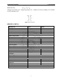
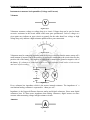
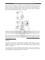
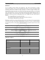
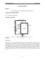
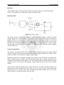
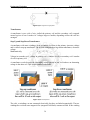
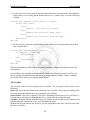
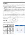
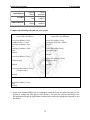
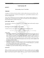
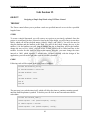
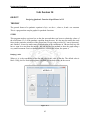
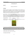
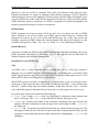
Engineering Workshop Lab Session 06 NED University of Engineering & Technology – Department of Computer & Information Systems Engineering Lab Session 06 OBJECT Demonstrating Printed Circuit Boards. THEORY In this lab we are going to implement a circuit on PCB( Printed Circuit Board). We are going to use the concepts built in the previous lab session regarding different aspects of PCB design. You have already implemented the circuit mentioned below in Fig 6.1 using breadboard / veroboard in previous lab session. We are going to implement the very same circuit with PCB in this lab session. VCC 5V To +15V R1 8 2 4 8 V (output) R2 OUT 3 6 555 2 + C 1 Figure 6.1 Patterning (etching) The vast majority of printed circuit boards are made by bonding a layer of copper over the entire substrate, sometimes on both sides, (creating a "blank PCB") then removing unwanted copper after applying a temporary mask (e.g. by etching), leaving only the desired copper traces. A few PCBs are made by adding traces to the bare substrate (or a substrate with a very thin layer of copper) usually by a complex process of multiple electroplating steps. The PCB manufacturing method primarily depends on whether it is for production volume or sample/prototype quantities. Circuit Schematics Imprint The print of the circuit depends on the requirement which can be categorize as follow: Commercial o silk screen printing–the main commercial method 50