1
FEDL86V7666-01
OKI Semiconductor
ML86V7666
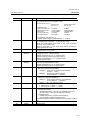
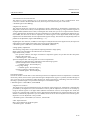
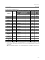
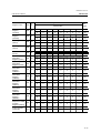
PIN DESCRIPTIONS
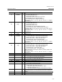
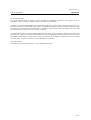
Attention: The input pin is not pull-down or pull-up in internal circuit.
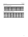
Pin
1
2
Symbol
ADGND
ADVDD
I/O
—
—
3
VIN1
I
4
VIN2
I
5
VIN3
I
6
VIN4
I
7
VIN5
I
8
VIN6
I
9
10
11
12
13
14
15
16
17
18
19
20
21
22
23
24
25
AVDD
AGND
REFP1
CM1
REFN1
REFP2
CM2
REFN2
AVDD
AGND
LPFOUT1
LPFOUT2
AVDD
AGND
ADVDD
ADGND
ADGND
—
—
O
O
O
O
O
O
—
—
O
O
—
—
—
—
—
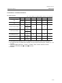
Description
ADC ground
ADC power supply
Composite-1 or S-video 1 luminance signal (Y-1) input
Connect to AGND when not used.
Composite-2 or S-video 2 luminance signal (Y-2) input
Connect to AGND when not used.
Composite-3 input
Connect to AGND when not used.
Composite-4 input
Connect to AGND when not used.
Composite-5 or S-video 1 chroma signal (C-1) input
Connect to AGND when not used.
S-video 2 chroma signal (C-2) input
Connect to AGND when not used.
Analog power supply
Analog ground
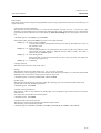
Ch1 ADC reference voltage (high)
Open
Ch1 ADC reference voltage (middle)
Open
Ch1 ADC reference voltage (low)
Open
Ch2 ADC reference voltage (high)
Open
Ch2 ADC reference voltage (middle)
Open
Ch2 ADC reference voltage (low)
Open
Analog power supply
Analog ground
Not used. Open
Not used. Open
Analog power supply
Analog ground
ADC power supply
ADC ground
ADC ground
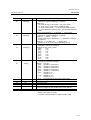
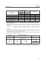
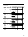
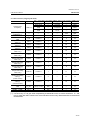
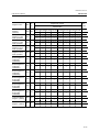
26
DVDD
—
Digital power supply
27
SCAN
I
Not used. Fixed at "0".
28
TEST [0]
I
Not used. Fixed at "0".
29
TEST [1]
I
Not used. Fixed at "0".
30
TEST [2]
I
31
SLEEP
I
32
RESET_L
I
33
34
35
36
37
|
44
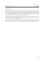
SCL
SDA
DVDD
DGND
C [9]
|
C [2]
I
I/O
—
—
O
Not used. Fixed at "0".
Sleep signal input. 0: Normal operation, 1: Sleep operation
The Input pin becomes ineffective at the sleep mode.
Reset signal input. 0: Reset, 1: Normal operation
After powering ON, be sure to reset.
I2C-bus clock input. "0" when not used.
I2C-bus data I/O pin. External pull up at 4.7 kΩ. "0" when not used.
Digital power supply
Digital ground
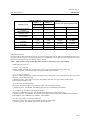
Data output C[9]:MSB - C[2] *)
ITU-R BT.656 mode: Hi-Z
10-bit Y/CbCr mode: Hi-Z
20-bit Y/CbCr mode: CbCr upper 8-bit data output
24-bit RGB mode: R 8-bit data output
24-bit component mode: Cr 8-bit data output
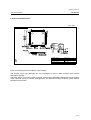
Add pins 45 and 46 in the 20-pin output mode.
The output mode is set by pins 85 and 86, or register
$00/MRA[7:6].
5/36