1
OKI Semiconductor
ML86V7666
FEDL86V7666-01
Issue Date: Apr. 21, 2004
NTSC/PAL Digital Video Decoder
USES AND APPLICATION EXAMPLES
The ML86V7666 is an IC that can be used as an interface for video signal input of any digital video processing
system. The device can be operated with a digital PLL line lock clock for applications where image quality is of
utmost importance. Further, for application where sync speed is important, such as switching between multiple
input channels, an asynchronous clock allows high-speed synchronous operation.
APPLICATION EXAMPLES
• TVs and TV reception equipment
Panel TVs such as TFT/PDP, PC TVs, digital TVs, set top boxes for receiving TV broadcasts
• Video recording equipment
DVD-R/W, HDD recorders, digital VTRs, digital video cameras, and digital cameras
• Monitoring systems
Multi-display equipment, long-playing video recording equipment, and transmission equipment for remote
monitoring
• PC peripheral equipment
Video capture boards, video editing equipment, and internet monitoring cameras
GENERAL DESCRIPTION
The ML86V7666 is an LSI that converts NTSC or PAL analog video signals into the YCbCr standard digital
format defined by ITU-R recommendations BT.601/BT.656 and RGB digital data.
The device has two built-in 10-bit A/D converter channels and can accept composite video and S-video signals as
input.
The composite video signal is separated into a luminance signal and chrominance signals by a 2-dimensional Y/C
separation filter (2-line or 3-line adaptive comb filter) and are then converted to a general-purpose video data
format.
With 1/4, 1/9, and 1/16 screen scaling features, the ML86V7666 is compatible with interfaces for a wide variety of
applications.
In addition to the asynchronous sampling that is a special feature of Oki decoders, video signals can also be
sampled using digital PLL for line lock clock sampling.
With asynchronous sampling, high-speed locking is available for synchronization and color bursts.
Further, due to the built-in pixel position correction circuit and the FIFO for correcting the pixel count, the video
jitter that can be a problem with asynchronous sampling is eliminated and jitter-free output data is ensured.
FEATURES
(z: New features not found in the MSM7664B; : Improved/altered features)
Input Section
{ Accepts NTSC/PAL composite video signals and S-video signals
{ Maximum 5 composite or 2 S-video + 2 composite inputs can be connected
{ Built-in clamp circuits and video amps
z Built-in 10-bit A/D converters (2 channels)
z Switchable between line lock clock sampling mode and asynchronous sampling mode
1/36
FEDL86V7666-01
OKI Semiconductor
ML86V7666
{ Operation mode : pixel frequencies (sampling clock: normal/double-speed)
NTSC/PAL ITU-R BT.601
: 13.5 MHz (13.5/27 MHz)
NTSC Square Pixel
: 12.272727 MHz (12.272727/24.545454 MHz)
NTSC 4fsc
: 14.31818 MHz (14.31818/28.63636 MHz)
PAL Square Pixel
: 14.75 MHz (14.75/29.5 MHz)
Digital Processing Section
2-dimensional Y/C separation using an adaptive comb filter (this filter is bypassed for S-video signal input)
NTSC/PAL system: 2-line or 3-line adaptive comb filter
Recognition of data in the VBI period (closed caption, CGMS, WSS) and function of reading from I2C-bus
(detection possible in all operating modes)
{ Copy protection (e.g., macrovision AGC and color stripe) detection
z Capable of decoding specially standardized signals such as NTSC443 and PAL-NM
{ Built-in AGC/ACC circuits (automatic luminance level control/automatic color level control)
{ Automatic NTSC/PAL recognition (only in the 27MHz mode)
Output Section
5 selectable output interfaces
ITU-R BT.656-4
: 10-bit(Y/CbCr) multiplexed data
With sync signals
10-bit Y/CbCr
: 10-bit(Y/CbCr) multiplexed data
YCbCr = 4:2:2 / YCbCr = 4:1:1
20-bit Y/CbCr
: 10-bit (Y) + 10-bit (CbCr) demultiplexed data YCbCr = 4:2:2 / YCbCr = 4:1:1
24-bit RGB
: 8-bit (R) + 8-bit (G) + 8-bit (B) demultiplexed data
24-bit component : 8-bit (Y) + 8-bit (Cb) + 8-bit (Cr) demultiplexed data
Output pixel count correction function via internal FIFO
{ Automatic FIFO/FIFO-through switching feature
z Screen scaling feature (fixed sizes: 1/4, 1/9, 1/16 and QVGA)
z Gamma correction function (only RGB output mode)
{ Sleep mode
{ Output pin Hi-Z mode
Other Sections
{ I2C-bus interface
{ 3.3V single power supply (5V input tolerance)
{ Package: 100-pin plastic TQFP (TQFP100-P-1414-0.50-K)
2/36
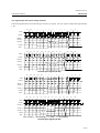
MODE[3:0]
Analog Block
Block Diagram
10bit ADC (ch1)
10bit ADC (ch2)
LPF
LPF
AMP/
Analog AGC
AMP/
Analog AGC
GAINS[2:0]
Decimation filter
Clamp
Chrominance
Input selector
INS[2:0]
M[2:0]
Decimation filter
RERP2
CM2
REFN2
LPFOUT2
Composite / Y
Input selector
VIN6
VIN5
VIN1
VIN2
VIN3
VIN4
REFP1
CM1
REFN1
LPFOUT1
SLEEP
ML86V7666
RESET_L
VREF
TEST[2:0]
Y
CLKSEL
CLKX2
VBID detection Block
C.C., WSS, CGMS,
Copy protection
HUE control
Digital ACC,
Chrominance
Block
Digital AGC,
Image filter,
Pixel position
Correction
Luminance
Block
Output format
Gamma correction,
Picture sizing,
Pixel count correction,
Output Block
CLKXO
CLKX2O
SCL
2
SDA
I C-bus control Block
Control register
•BT.656 10-bit multiplexed data
•Y/CbCr 10-bit multiplexed data
•Y/CbCr 20-bit demultiplexed data
•Y/Cb/Cr 24-bit demultiplexed data
•R/G/B 24-bit demultiplexed data
Synchronization Block
PLLSEL
STATUS1
STATUS2
Data width
[9:0] 10bit
[9:2] 8bit
Cb [9:2]
B [9:2]
CbCr [9:0]
Cr [9:2]
R [9:2]
YCbCr [9:0]
Y [9:0]
Y [9:2]
G [9:2]
VHVAL/SCALW
CSYNC/SCALR
VVALID
HVALID
ODD/EVEN
VSYNC_L
HSYNC_L
OKI Semiconductor
SCAN
Test control
Block
C
C
2line or 3line
Adaptive comb
filter
2Dim.
Y/C separation
Block
PLL Block
LPF
FEDL86V7666-01
ML86V7666
BLOCK DIAGRAM
3/36
FEDL86V7666-01
OKI Semiconductor
ML86V7666
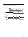
PIN CONFIGURATION (TOP VIEW)
VIN3
5
VIN4
6
VIN5
7
STATUS2
CSYNC/ SCALR
VHVAL/ SCALW
PLLSEL
77
76
80
78
STATUS1
81
79
M[1]
M[2]
82
84
83
MODE[3]
DGND
M[0]
85
86
88
87
GAINS[2]
MODE[0]
MODE[1]
MODE[2]
89
90
93
INS[2]
INS[1]
94
GAINS[0]
GAINS[1]
INS[0]
95
91
DVDD
96
92
PVDD
DGND
97
98
PGND
3
DIGITAL
ADC
4
VIN6
8
AVDD
9
AGND
10
REFP1
CM1
11
REFN1
REFP2
13
ANALOG
12
DIGITAL
16
49
50
B[2]
44
48
43
C[2]
B[5]
B[4]
B[3]
41
C[5]
C[4]
C[3]
47
40
C[6]
46
39
C[7]
C[0]/B[6]
38
C[8]
45
37
C[9]
C[1]/B[7]
36
DGND
42
35
DVDD
DIGITAL
34
25
SDA
ADGND
ADC
33
24
SCL
ADGND
32
23
31
ADVDD
SLEEP
RESET_L
22
TEST[2]
21
AGND
30
AVDD
ANALOG
29
20
28
LPFOUT2
TEST[1]
19
TEST[0]
LPFOUT1
27
18
26
AGND
CLKX2
73
DGND
72
DVDD
71
CLKX2O
70
CLKXO
69
ODD/EVEN
HSYNC_L
67
VSYNC_L
66
VVALID
65
HVALID
DGND
62
DVDD
Y[9]
61
Y[8]
60
Y[7]
59
Y[6]
58
Y[5]
63
15
17
CLKSEL
74
64
ADC
14
AVDD
75
68
SCAN
CM2
PLL
2
VIN1
VIN2
REFN2
LPF
VREF
100
1
DVDD
ADGND
ADVDD
99
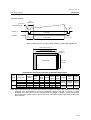
100-Pin Plastic TQFP (TQFP100-P-1414-0.50-K)
57
Y[4]
56
Y[3]
55
Y[2]
54
Y[1]/B[0]
53
Y[0]/B[1]
52
DGND
51
DVDD
4/36
FEDL86V7666-01
OKI Semiconductor
ML86V7666
PIN DESCRIPTIONS
Attention: The input pin is not pull-down or pull-up in internal circuit.
Pin
1
2
Symbol
ADGND
ADVDD
I/O
—
—
3
VIN1
I
4
VIN2
I
5
VIN3
I
6
VIN4
I
7
VIN5
I
8
VIN6
I
9
10
11
12
13
14
15
16
17
18
19
20
21
22
23
24
25
AVDD
AGND
REFP1
CM1
REFN1
REFP2
CM2
REFN2
AVDD
AGND
LPFOUT1
LPFOUT2
AVDD
AGND
ADVDD
ADGND
ADGND
—
—
O
O
O
O
O
O
—
—
O
O
—
—
—
—
—
Description
ADC ground
ADC power supply
Composite-1 or S-video 1 luminance signal (Y-1) input
Connect to AGND when not used.
Composite-2 or S-video 2 luminance signal (Y-2) input
Connect to AGND when not used.
Composite-3 input
Connect to AGND when not used.
Composite-4 input
Connect to AGND when not used.
Composite-5 or S-video 1 chroma signal (C-1) input
Connect to AGND when not used.
S-video 2 chroma signal (C-2) input
Connect to AGND when not used.
Analog power supply
Analog ground
Ch1 ADC reference voltage (high)
Open
Ch1 ADC reference voltage (middle)
Open
Ch1 ADC reference voltage (low)
Open
Ch2 ADC reference voltage (high)
Open
Ch2 ADC reference voltage (middle)
Open
Ch2 ADC reference voltage (low)
Open
Analog power supply
Analog ground
Not used. Open
Not used. Open
Analog power supply
Analog ground
ADC power supply
ADC ground
ADC ground
26
DVDD
—
Digital power supply
27
SCAN
I
Not used. Fixed at "0".
28
TEST [0]
I
Not used. Fixed at "0".
29
TEST [1]
I
Not used. Fixed at "0".
30
TEST [2]
I
31
SLEEP
I
32
RESET_L
I
33
34
35
36
37
|
44
SCL
SDA
DVDD
DGND
C [9]
|
C [2]
I
I/O
—
—
O
Not used. Fixed at "0".
Sleep signal input. 0: Normal operation, 1: Sleep operation
The Input pin becomes ineffective at the sleep mode.
Reset signal input. 0: Reset, 1: Normal operation
After powering ON, be sure to reset.
I2C-bus clock input. "0" when not used.
I2C-bus data I/O pin. External pull up at 4.7 kΩ. "0" when not used.
Digital power supply
Digital ground
Data output C[9]:MSB - C[2] *)
ITU-R BT.656 mode: Hi-Z
10-bit Y/CbCr mode: Hi-Z
20-bit Y/CbCr mode: CbCr upper 8-bit data output
24-bit RGB mode: R 8-bit data output
24-bit component mode: Cr 8-bit data output
Add pins 45 and 46 in the 20-pin output mode.
The output mode is set by pins 85 and 86, or register
$00/MRA[7:6].
5/36
FEDL86V7666-01
OKI Semiconductor
ML86V7666
Pin
45
46
Symbol
C[1]/B[7]
C[0]/B[6]
I/O
O
47
|
50
B [5]
|
B [2]
O
51
DVDD
—
52
53
54
DGND
Y [0]/B [1]
Y [1]/B [0]
—
O
55
|
62
Y [2]
|
Y [9]
O
63
64
65
DVDD
DGND
HVALID
—
—
O
66
VVALID
O
67
68
69
VSYNC_L
HSYNC_L
ODD/EVEN
O
O
O
70
CLKXO
O
71
CLKX2O
O
72
73
DVDD
DGND
—
—
Description
Data output C[1]-C[0]LSB or B[7]MSB-B[6] *)
ITU-R BT.656 mode: Hi-Z
10-bit Y/CbCr mode: Hi-Z
20-bit Y/CbCr mode: CbCr lower 2-bit output
24-bit RGB mode: B upper 2-bit output
24-bit component mode: Cb upper 2-bit output
The output mode is set by pins 85 and 86, or register
$00/MRA[7:6].
Data output B[5] - B[2] *)
ITU-R BT.656 mode: Hi-Z
10-bit Y/CbCr mode: Hi-Z
20-bit Y/CbCr mode: Hi-Z
24-bit RGB mode: B intermediate 4-bit output
24-bit component mode: Cb intermediate 4-bit output
For upper 2 bits, pins 45 and 46 are used, for lower 2 bits, pins 53
and 54 are used.
The output mode is set by pins 85 and 86, or register
$00/MRA[7:6].
Digital power supply
Digital ground
Data output Y[1]-Y[0]LSB or B[1]-B[0]LSB *)
ITU-R BT.656 mode: YCbCr lower 2-bit data output
10-bit Y/CbCr mode: YCbCr lower 2-bit data output
20-bit Y/CbCr mode: Y lower 2-bit data output
24-bit RGB mode: B lower 2-bit data output
24-bit component mode: Cb lower 2-bit data output
The output mode is set by pins 85 and 86, or register
$00/MRA[7:6].
Data output Y[9]: MSB - Y[2] *)
ITU-R BT.656 mode: YCbCr upper 8-bit data output
10-bit Y/CbCr mode: YCbCr upper 8-bit data output
20-bit Y/CbCr mode: Y upper 8-bit data output
24-bit RGB mode: G 8-bit data output
24-bit component mode: Y 8-bit data output
When performing 10-bit output in BT.656 / (Y/CbCr) output mode,
add pins 53 and 54.
The output mode is set by pins 85 and 86, or register
$00/MRA[7:6].
Digital power supply
Digital ground
Horizontal valid pixel timing signal output *)
"H" is output for horizontal valid data section.
Vertical valid line timing signal output *)
"H" is output for vertical valid data section.
Vertical sync signal output (V sync) *)
Horizontal sync signal output (H sync) *)
Field display output *)
"H" is output for ODD field section.
Pixel clock output
Double-speed clock mode (Pin 75 =0)
One half of system clock frequency is output.
Normal clock mode (Pin 75 = 1)
The same frequency as system clock frequency is output.
Operating clock output
The same frequency as the Operating mode clock frequency is
output.
Digital power supply
Digital ground
6/36
FEDL86V7666-01
OKI Semiconductor
Pin
74
ML86V7666
Symbol
CLKX2
I/O
I
Description
System clock input
Input a fixed clock or a PLL reference clock.
Fixed clock (Pin 76 = 0)
Operating mode
NTSC ITU-R BT. 601
NTSC Square Pixel
NTSC 4Fsc
PAL ITU-R BT. 601
PAL Square Pixel
75
CLKSEL
I
76
PLLSEL
I
77
VHVAL
/SCALW
O
78
CSYNC
/SCALR
O
79
STATUS2
O
80
STATUS1
O
81
M [2]
I
82
M [1]
I
83
M [0]
I
84
DGND
—
Normal clock
(Pin 75 = 1)
Double-speed clock
(Pin 75 = 0)
13.5 MHz
12.272727 MHz
14.31818 MHz
13.5 MHz
14.75 MHz
27 MHz
24.545454 MHz
28.63636 MHz
27 MHz
29.5 MHz
PLL reference clock (Pin 76 = 1)
Register $1F/PLLR[0] 0:32 MHz(default) 1: 25 MHz
Double-speed clock select pin
0: Double-speed clock mode 1: Normal clock mode
When the double-speed clock mode is set, input a doubled
frequency to the system clock.
When Pin 76 PLLSEL = 1 (PLL clock mode), set to 0 to select the
double-speed clock mode.
PLL clock select pin
0: Fixed clock 1: PLL clock
Register $1A/SCR[7:6] = 00 (When scaling is not used.)
VHVAL (VVALID ∧ HVALID) output
Register $1A/SCR[7:6] = 01-11 (scaling mode)
External memory writing control signal output
Register $18/OMRD[5:4] = 01-11 (QVGA mode)
QVGA clock is output.
Register $1A/SCR[7:6] = 00 (When scaling is not used.)
CSYNC (Composite SYNC) output
Register $1A/SCR[7:6] = 01-11 (scaling mode)
External memory read control signal output
Status signal output
Selected by register $15/OMRA[0].
OMR[0]:0 NTSC-PAL recognition output (default)
0: NTSC 1: PAL
OMR[0]:1 HLOCK sync detection output
0: Non-detection 1: Detection
Status signal output
Selected by register $15/OMRA[1]
OMR[1]: 0 FIFO overflow detection output (default)
0: Non-detection 1: Detection
OMR[1]: 1 PLL sync detection output
I2C-bus slave address select "0" when not used.
0: 1000 001X (X: 0 = Write, 1 = Read)
1: 1000 011X (X: 0 = Write, 1 = Reed)
Amplifier gain setting and input pin switch setting control select pin
0: External pin mode
Amplifier gain setting: Pins 89 to 91 GAINS[2:0] are used
Input pin setting: Pins 92 to 94 INS[2:0]) are used
1: Register mode
Amplifier gain setting: Register $1E/ADC2[6:4]
Input pin setting: Register $1D/ADC1[2:0]
The internal register setting is invalid when the external pin mode is
set.
Not used. Fixed at "0".
Digital ground
7/36
FEDL86V7666-01
OKI Semiconductor
ML86V7666
Pin
85
86
Symbol
MODE [3]
MODE [2]
I/O
I
87
88
MODE [1]
MODE [0]
I
89
|
91
GAINS [2]
|
GAINS [0]
I
92
|
94
INS [2]
|
INS [0]
I
95
96
97
98
99
DVDD
DGND
PVDD
VREF
LPF
—
—
—
O
I
100
PGND
—
Description
Output mode external setting pins "0" when not used.
Valid when register $00/MRA[0] = 0 (default).
MODE [3:2]
00: ITU-R BT.656 (10-bit Y/CbCr + SAV, EAV, blank)
01: 10-bit Y/CbCr (10-bit Y/CbCr multiplexed data)
10: 20-bit Y/CbCr (10-bit Y + 10-bit CbCr demultiplexed data)
11: 24-bit RGB/YCbCr (RGB or YCbCr 8+8+8-bit demultiplexed
data)
Register $10/CHRCB[1] = 0: 24-bit RGB, 1: 24-bit YCbCr
Operation mode external setting pins "0" when not used.
Valid when register $00/MRA[0] = 0 (default).
MODE [1] 0: NTSC, 1: PAL
Invalid when register $02/MRC[7] = 1 (NTSC/PAL automatic
recognition).
MODE [0] 0: ITU-R BT. 601, 1: Square Pixel
NTSC 4fsc can be set by register $00/MRA[5:3] only.
Amplifier gain external setting pins "0" when not used.
Valid when external pin 82 M[1]=0.
GAINS [2:0] Gain value (x times)
[000]
0.55
[001]
0.70
[010]
0.93
[011]
1.21
[100]
1.60
[101]
2.09
[110]
2.65
[111]
3.45
Input pin switch external setting pins "0" when not used.
Valid when external pin 82 M[1]=0.
INS[2:0] Input pin
[000]
VIN1(Pin 3) Composite-1
[001]
VIN2(Pin 4) Composite-2
[010]
VIN3(Pin 5) Composite-3
[011]
VIN4(Pin 6) Composite-4
[100]
VIN5(Pin 7) Composite-5
[101]
VIN1(Pin 3) Y-1
VIN5(Pin 7) C-1
[110]
VIN2(Pin 4) Y-2
VIN6(Pin 8) C-2
[111]
Prohibited setting (ADC enters sleep mode)
Digital power supply
Digital ground
PLL power supply
Center frequency setting pin "0" when not used.
Analog PLL loop filter connection pin "0" when not used.
Refer to the sample circuits provided in the User's Manual.
PLL ground
*) Leave open when not used.
Connect a pull-up resistor in High-Z output mode .
8/36
FEDL86V7666-01
OKI Semiconductor
ML86V7666
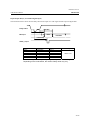
FUNCTIONAL DESCRIPTION
This section explains the basic functions of the IC in terms of the blocks shown in the block diagram.
Refer to the User's manual for detailed explanations of the internal registers and any functions that are not covered
in this data sheet.
Analog Section
The analog section inputs video signals. The analog section uses the video signal channel selector, AMP and 10-bit
ADC to select the desired channel from among several video signals and convert the input to digital video data.
Analog input selector:
The analog input selector is compatible with composite signals and S-video signals. The maximum number of
input connections is 5 channels of composite signals or 2 channels of S-video signals + 2 channels of composite
signals. The selection of these input connections can be changed by external pins or by register controls using
the I2C-bus.
# Related register: $1D/ADC1[2:0]
Analog Input Conditions
Control pin
Register
Input signal
Pin 82 M[1]=0
Pin 82 M[1]=1
Composite-1 input*
Composite-2 input
Composite-3 input
Composite-4 input
INS[2:0]
[000]
[001]
[010]
[011]
ADC1[2:0]
[000]*
[001]
[010]
[011]
Composite-5 input
[100]
[100]
S-video-1 input
S-video-2 input
All inputs OFF
[101]
[110]
[111]
[101]
[110]
[111]
Blank spaces: Non-selectable;
Input pin
VIN1
VIN2
VIN3
VIN4
ADC operation
VIN5
VIN6
Composite
ON
ON
ON
ON
OFF
OFF
OFF
OFF
Composite
ON
OFF
Chroma
ON
ON
OFF
ON
ON
OFF
Composite
Composite
Composite
Luminance
Y ADC C ADC
Luminance
Chroma
OFF (ADC sleep)
*: Register default setting after LSI reset
Clamp function:
The clamp fixes the video input signal in the ADC input range. Clamping is performed by sync chip clamp.
AMP/analog AGC function:
This function converts video input signals to the optimum level for the ADC using the analog AMP of the AGC
function. The AGC function has an output level adjust function in the luminance block of the digital section in
addition to the AMP input level adjust function. Manual setting of the AMP gain is also possible.
# Related register: $1E/ADC2
Analog AMP Manual Gain Control
82-pin M[1] = 0
82-pin M[1] = 1
Gain setting pin
GAINS[2:0]
[000]
[001]
[010]
[011]
[100]
[101]
[110]
[111]
Register
$1E/ADC2[6:4]
[000]
[001]
[010]*
[011]
[100]
[101]
[110]
[111]
Gain setting value
Typical value
(multiplication factor)
0.55
0.70
0.93
1.21
1.60
2.09
2.65
3.45
82-pin M[1] pin = "0": External pin analog gain setting mode
"1": Internal register analog gain setting mode
9/36
FEDL86V7666-01
OKI Semiconductor
ML86V7666
A/D converter:
This 10-bit A/D converter (ADC) converts analog video signals to digital video data. There are 2 channels
built into the ADC. Sampling is performed at the pixel frequency or double-speed. In the S-video input mode,
both channels of the A/D converter operate; in the composite input mode, only one channel operates, and the
A/D converter on the chrominance signal input side goes OFF.
# Related registers: $00/MRA, $1D/ADC1
Digital Section
The digital section separates the video data digitized by the ADC into Y and C data, converts these data to
various data formats and outputs them. The digital section also performs output level adjustment, image quality
adjustment and various corrections.
Decimation filter:
The decimation filter is used in the double-speed sampling mode. Because internal processing is performed at
single speed also in the double-speed sampling mode, this filter is needed to reduce the data that has been
doubled by one-half. Using the decimation filter after double-speed sampling reduces high-frequency noise
and makes it possible to obtain data with a good high-frequency characteristic.
# Related register: $02/MRC[4]
2-dimensional Y/C separation block:
This block separates composite data into Y (luminance) data and C (chrominance) data. For S pin input, Y/C
separation circuit is bypassed.
• 2-Dimensional Y/C Separation Function
With the Y/C separation filter, composite data is separated into Y (luminance) data and C (chrominance) data.
There are various Y/C separation filters available, which can be selected in an internal register.
# Related register: $01/MRB
$01/MRB[5:3]
*000
001
010
011
100
101
110
111
NTSC Y/C separation
2-line/3-line adaptive comb filter
3-line comb filter
Trap filter
3-line comb/trap adaptive filter
3-line comb/trap adaptive filter 2
2-line/3-line adaptive transition filter
Undefined
Undefined
PAL Y/C separation
2-line comb/trap adaptive transition filter
2-line comb filter
Trap filter
Undefined
Undefined
Undefined
Undefined
2-line/3-line adaptive comb filter
• Special Broadcast Standards Decoder Function
In addition to normal NTSC/PAL signals, this decoder can decode the following specialized signals.
Set register $01/MRB[5:3] to ”010”, ”011”, “100”, or “111” when using the PAL M,N mode.
# Related register: MRA[2:1] $00
MRA[2:1] = 00 Normal mode *
MRA[2:1] = 01 NTSC443
MRA[2:1] = 10 PAL M, N
MRA[2:1] = 11 Undefined
Luminance block:
The luminance block removes sync signals from the luminance data after Y/C separation, and performs
adjustments such as luminance level adjustment and luminance image quality correction and adjustment. The
digital decoded data that is output conforms with ITU-R BT601.
10/36
FEDL86V7666-01
OKI Semiconductor
ML86V7666
• Pixel Position Correction Function
This function corrects sampling error in asynchronous sampling and loss of PLL synchronization. Error
correction is made in the horizontal direction, which improves vertical line jitter on the screen.
# Related register: $02/ MRC[6]
• Digital AGC Function
This function adjusts the output level of luminance signals. Adjustment is automatically performed by the
digital AGC (Auto Gain Control), but the adjustment can also be set manually by using an internal register to
set digital MGC (Manual Gain Control). In the digital AGC mode, the sync level is compared with a reference
value to determine the amplification rate of the luminance level. The default is automatically adjusted to sync
level 40IRE, but the level can also be adjusted in an internal register. In the digital MGC mode, the signal
amplification rate and the black level are adjusted with register settings. The black level is adjusted by means of
pedestal level adjustment (register $0E/SSEPL[7] = "1").
Regarding the AGC function, in addition to the output level adjust function in the digital section, the input level
adjust function of the AMP in the analog section also operate independently.
# Related registers: $0B/AGCL, $0C/AGCRC, $0E/SSEPL, $0D/CLC
• Image Quality Adjustment
The following image filters are provided for adjusting luminance image quality.
Refer to the User's Manual for the characteristics of each filter.
Edge enhancement pre-filter
This pre-filter enhances the edges of luminance component signals; the pre-filter and the sharp filter
operate at the same time.
# Related register: $0A/LUMC[7]
Aperture bandpass filter and coring filter for contour compensation
Adjustment is made through a combination of the following registers:
Aperture bandpass filter coefficient setting
# Related register: $0A/LUMC[6:5]
Coring range setting
# Related register: $0A/LUMC[4:3]
Aperture weighting coefficient setting
# Related register: $0A/LUMC[2:0]
Chrominance block:
This block decodes chroma data to Cb/Cr data and performs level adjustment and color adjustment. To eliminate
unnecessary bands, this block first passes data through a bandpass filter (bypass is possible) and then through an
ACC correction circuit to maintain a stable chroma level, before performing UV decoding. The result of the UV
decoding is passed through a low-pass filter and output as a chrominance signal.
# Related registers: $0F/CHRCA, $10/CHRCB
• Digital ACC Function
The digital ACC is the gain adjustment for the chrominance signal output level. Adjustment is automatically
performed by the digital ACC (Auto Chrominance Control), but the adjustment can also be set manually by
using an internal register to set digital MCC (Manual Chrominance Control). In the digital ACC mode, the
burst level is compared with a reference value to determine the amplification rate of the chrominance level. The
default is automatically adjusted to sync level 40IRE, but the level can also be adjusted in an internal register.
Separate U/V level adjustment is also possible.
# Related registers: $0F/CHRCA, $11/ACCC, $12/ACCRC
• Hue Adjust Function
Hues can be adjusted in the HUE register.
# Related register: $13/HUE
11/36
FEDL86V7666-01
OKI Semiconductor
ML86V7666
Output block:
The output block performs output timing adjustment, picture sizing, output format conversion, and other types of
output conversion.
• Pixel Count Correction Function
This function uses the internal FIFO to correct the total number of pixels in a line. It corrects the 1-line
sampling error generated when in asynchronous sampling mode or PLL synchronization is lost, and fixes the
pixel count for a line within the active screen. Refer to Active Pixel Timing for more on the pixel count for one
line.
# Related registers: $03/MRD[7:6], $16/OMRB
In the FIFO mode, register $03/MRD[7:6] can be set to bypass the FIFO.
MRD[7:6] = 00: FIFO-1 mode * (default)
Uses the internal FIFO to output data with the pixel count for 1H in the active screen as
the reference value.
MRD[7:6] = 01: FIFO-2 mode *
Uses the internal FIFO to set and output the pixel count per 1H as the reference value.
The internal processing method is different from the FIFO-1 mode. This mode is
effective for non-standard signals.
MRD[7:6] = 10: FIFO through mode
This mode does not use the internal FIFO for pixel count correction, but outputs the
decoded input signal as it is.
MRD[7:6] = 11: Undefined
• Scaling Function
This function shrinks the screen (fixed value).
Scaling
This function converts the input image to 1/4, 1/9, or 1/16 size for output.
Field memory control signals (pin 77 SCALW and pin 78 SCALR) are provided, so in connection with the Oki
4M-FIFO, a sub-screen can be output at any location on the screen.
# Related registers: $1A/SCR, $1B/SCVPR, and $1C/SCHPR
QVGA output
This function performs QVGA conversion where the operating clock was used in the Square Pixel mode.
QVGA data is output by decimating the pixels.
# Related register: $18/OMRD
• Gamma Correction Function
This function, which is only effective for RGB output, corrects gamma as part of the correction of monitor
characteristics.
Five stages can be selected in an internal register.
# Related register: $18/OMRD
• Output Format Conversion Function
This function converts the output data to the desired output format.
The following output formats are possible.
# Related registers: $00/MRA, $02/MRC, $03/MRD, $10/CHRCB, $18/OMRD, and $1A/SCR
12/36
FEDL86V7666-01
OKI Semiconductor
ML86V7666
Output Formats
Output mode
(i): interlace
ITU-R BT.656 (i) 4:2:2
Y/CbCr 10-bit multiplex (i) 4:2:2
Y/CbCr 20-bit de-multiplex (i) 4:2:2
Y/CbCr 20-bit de-multiplex (i) 4:1:1
RGB-24bit de-multiplex (i) 4:4:4
not use
Component (YCbCr) 24-bit
de-multiplex (i) 4:4:4
not use
Register
$00/MRA[0]=0
Control pin
(Pins 85, 86)
MODE[3:2]
[00]
[01]
[10]
[10]
[11]
[11]
Register
$00/MRA[0]=1
$00/MRA[7:6]
[00]
[01]
[10]
[10]
[11]
[11]
$02/MRC[5]
0
0
0
1
0
0
$10/CHRCB[1]
0
0
0
0
0
0
[11]
[11]
0
1
[11]
[11]
0
1
Register
Register
• Synchronization Block
This block controls the sync signals for internal operation, output sync signals, and the timing for each block.
Synchronization detection levels, output timing, and various other functions can be adjusted by the registers
listed below.
# Related registers: $03/MRD, $04/SYDR, $06/STHR, $07/HSDL, $08/HVALT, $09/VVALT,
$0F/CHRCA, $10/CHRCB, $14/BBHC, $15/OMRA, $17/OMRC, and $18/OMRD
PLL Function
The digital PLL circuit generates an operating clock synchronized with the horizontal sync signals of the video
signals. With the input of a 25 MHz or 32 MHz standard clock, the double-speed sampling clock for each mode
is provided as a line lock clock and used as the system clock.
The asynchronous sampling mode, which uses an asynchronous clock directly, can be used without using PLL.
# Related registers: $17/OMRC, $1F/PLLR
Input Clock Settings
76pin
PLLSEL
Input clock
Sampling clock
PLLSEL=0
Fixed clock mode
Sampling clock input according to the operating mode
(See the table below)
Asynchronous clock
PLLSEL=1
PLL clock mode
$1F/ PLLR[0]=0*
32 MHz
$1F/ PLLR[0]=1
25 MHz
$1F/ PLLR[7]=0*
PLL ON
Line lock clock
$1F/ PLLR[7]=1
PLL OFF
Asynchronous clock
*: Default
In the PLL clock mode, a double-speed line lock clock is generated by setting the operating mode.
13/36
FEDL86V7666-01
OKI Semiconductor
ML86V7666
Operating Modes / Sampling Clock Settings
MRA[0] = 0 *
Operating mode
NTSC ITU-R BT.601
13.5 MHz
NTSC Square pixel
12.272727 MHz
NTSC 4fsc
14.31818 MHz
—
PAL ITU-R BT.601
13.5 MHz
PAL Square pixel
14.75 MHz
—
—
— : Not used
MRA[0] = 1
Sampling clock (double-speed/normal)
Control pin
(pin 87 or 88)
MODE[1:0]
MRA[5:3]
[00]
[000]
27 MHz
13.5 MHz
[01]
[001] *
24.545454 MHz
12.272727 MHz
—
[010]
28.63636 MHz
14.31818 MHz
—
[011]
—
—
[10]
[100]
27 MHz
13.5 MHz
[11]
[101]
29.5 MHz
14.75 MHz
—
—
[110]
[111]
—
—
—
—
Register
75-pin CLKSEL=0 75-pin CLKSEL=1
*: Default
VBID detection block:
This block detects data information and copy protection information from the VBI (Vertical Blanking Interval) of
the input luminance signals. The following four types of VBID data can be detected, and the detection line and
detection level can be changed by altering register settings.
*Note: VBID detection may not provide 100% detection, depending on the signal status.
VBID Detection Function
(1) AGC copy protection
Detects whether specified lines include a macrovision AGC pulse (NTSC/PAL) and sets a flag.
# Related registers: $24/AGCD1, $25/AGCD2, $27/AIREG, $29/VFLAG
(2) C. C. (Closed Caption)
Detects whether specified lines include closed caption data (NTSC/PAL), keeps separately the data of even and
odd lines, and sets individual flags.
# Related registers: $20/CCD1, $21/CCD2, $27/AIREG, $29/VFLAG, $2A/CCDO0, $2B/CCDO1,
$2C/CCDE0, and $2D/CCDE1
(3) WSS (Wide Screen Signaling)
Detects the WSS data in the lines specified by ETSC and sets a flag (PAL only).
# Related registers: $26/WSSD, $27/AIREG, $29/VFLAG, $34/WSSD0, $35/WSSD1
(4) CGMS (Copy Generation Management System)
Detects the CGMS data in the lines specified by IEC61880 and sets a flag (NTSC only).
# Related registers: $22/CGMS1, $23/CGMS2, $27/AIREG, $29/VFLAG, $2E/CGMSO0, $2F/CGMSO1,
$30/CGMSO2, $31/CGMSE0, $32/CGMSE1, $33/CGMSE2
(5) Other copy protection detection functions
Detects the color stripes, false pulses, and MV protection and sets flags.
# Related registers: $27/AIREG, $28/STATUS, $29/VFLAG
14/36
FEDL86V7666-01
OKI Semiconductor
ML86V7666
I2C-bus control block:
This serial interface block is based on the I2C standard of the Phillips Corporation. The registers at up to
subaddress 27h are write/read, while the registers from 28h on are read-only.
Normally, a license from the Phillips Corporation allowing the use of its I2C patent is required to use an I2C bus.
However, the license to use this LSI chip as a slave is granted by the Phillips Corporation upon purchasing this LSI
chip. There is no need for a license if the decoder is used alone, without I##2C control, but if this I##2C-bus is used
to control this LSI, a license for use as a master is required.
As of 2001, the I2C patent expired in Japan and the rest of the Asian region, so there have been no costs with regard
to license fees. However, in the USA and Canada, there is still a requirement for the payment of license fees, so if
this product is intended for overseas trade, it may be necessary to pay the Phillips Corporation license fees for the
use of its patent. For more information, contact the Phillips Corporation.
Test control block:
This block is used to test the LSI chip. It is not intended for user use.
15/36
FEDL86V7666-01
OKI Semiconductor
ML86V7666
ABSOLUTE MAXIMUM RATINGS
Parameter
Power supply
voltage
Input voltage
Power
consumption
Storage
temperature
Symbol
Condition
Rating
Unit
VDD
Ta = 25°C
–0.3 to 4.5
V
Vi
VDD = 3.3 V
–0.3 to 5.5
V
Pw
—
1
W
Tstr
—
–55 to 150
°C
RECOMMENDED OPERATING CONDITIONS
Parameter
Power supply
voltage
Power supply
voltage
Analog video
signal input
Operating
temperature (*)
Symbol
Condition
Min.
Typ.
Max.
Unit
VDD
—
3.0
3.3
3.6
V
GND
—
—
0
—
V
Vain
SYNC tip to
white peak
level
0.8
1.1
Vp-p
Ta
—
-40
85
°C
—
(*): The Operating temperature is the ambient temperature.
16/36
FEDL86V7666-01
OKI Semiconductor
ML86V7666
ELECTRICAL CHARACTERISTICS
DC Characteristics
Parameter
“H” level input voltage
(*3)
“L” level input voltage
(*3)
Symbol
Vih1
Vih2
( *1 )
Vil
(Ta = -40 to +85°C, VDD (DVDD, ADVDD, AVDD) = 3.0 V to 3.6 V)
Condition
Min.
Typ.
Max.
Unit
—
2.2
—
VDD( *2 )
V
—
0.8 VDD
—
VDD( *2 )
V
—
0
—
0.8
V
0.7 VDD
—
VDD
V
0
—
0.6
V
–10
—
10
µA
–10
—
10
µA
0.4
—
1.3
Vp-p
Ioh = –4 mA
(*4)
"H" level output voltage
"L" level output voltage
Voh
Vol
Input leakage current
Ii
Output leakage current
Io
Analog input
Avin
Ioh = –8 mA
(*5)
Iol = 4mA
(*4)
Iol = 8 mA
(*5)
Vi = GND to
VDD
Vi = GND to
VDD
C
Coupling
*1. SDA, CLKX2
*2. The inputs have a tolerance of 5V, so applying 5V to the inputs will not cause a problem.
*3. The input pins are not pulled down internally, so they should not be left open; at either a “L” or a
“H” level.
*4: Y[9:0],C[9:0],B[5:2],HSYNC L, VSYNC L, SYSSEL, ODD, VVALID, HVALID, CLKXO,
STATUS1, STATUS2, SCALW, SCALR, SDA, SCL
*5: CLKX2O
17/36
FEDL86V7666-01
OKI Semiconductor
ML86V7666
Current Characteristics
Parameter
Symbol
Digital power
supply current
(DVDD)
1 channel
operating
IDD1
Analog power
supply current
(AVDD + ADVDD)
1 channel
operating
Digital power
supply current
(DVDD)
2 channel
operating
Analog power
supply current
(AVDD + ADVDD)
2 channel
operating
Digital power
supply current
(DVDD)
1 channel
operating
Analog power
supply current
(AVDD + ADVDD)
1 channel
operating
Digital power
supply current
(DVDD)
2 channel
operating
(Ta = -40 to +85°C, VDD (DVDD, ADVDD, AVDD) = 3.0 V to 3.6 V, GND = 0 V)
Min.
Typ.
Max.
Condition
Operating clock
Unit
VDD = 3.0 V VDD = 3.3 V VDD = 3.6 V
24.545454 MHz
75
105
155
PLL Mode
CLKX2 = 32
MHz
AD1 on
AD2 off
IDA1
27 MHz
80
110
160
28.63636 MHz
85
115
165
29.5 MHz
85
120
170
30
45
65
24.545454 MHz
70
95
145
mA
24.545454 MHz
27 MHz
28.63636 MHz
mA
29.5 MHz
IDD2
27 MHz
75
100
150
28.63636 MHz
80
105
155
29.5 MHz
85
110
160
55
75
95
24.545454 MHz
70
95
150
27 MHz
75
100
155
Fixed Clock
Mode
28.63636 MHz
80
105
160
29.5 MHz
80
110
165
AD1 on
AD2 off
24.545454 MHz
30
45
65
65
90
140
PLL Mode
CLKX2 = 32
MHz
AD1 on
AD2 on
IDA2
mA
24.545454 MHz
27 MHz
28.63636 MHz
mA
29.5 MHz
IDD1
IDA1
27 MHz
28.63636 MHz
mA
mA
29.5 MHz
24.545454 MHz
IDD2
Analog power
supply current
(AVDD + ADVDD)
2 channel
operating
IDA2
Power supply
current
(inactive)
IDoff
27 MHz
70
95
145
Fixed Clock
Mode
28.63636 MHz
75
100
150
29.5 MHz
80
105
155
AD1 on
AD2 on
24.545454 MHz
55
75
95
mA
—
—
20
mA
27 MHz
28.63636 MHz
mA
29.5 MHz
Vi = 1.5 V
18/36
FEDL86V7666-01
OKI Semiconductor
ML86V7666
AC Characteristics (Double-Speed Mode)
Parameter
Symbol
CLKX2 Cycle
Frequency
1/tclkx2
Input Frequency
Tolerance (**)
CLKX2 Duty
CLKX2 Rise/Fall
Time
Output Data Delay
Time 1(*)
Output Data Delay
Time 2(*)
Output Data Delay
Time 3(*)
Output Data Delay
Time 1x1(*)
Output Data Delay
Time 1x2(*)
Output Data Delay
Time 1x3(*)
Output Data Delay
Time 2x1(*)
Output Data Delay
Time 2x2(*)
Output Data Delay
Time 2x3(*)
Output Clock Delay
Time (*)
(CLKX2-CLKXO)
Output Clock Delay
Time (*)
(CLKX2-CLKX2O)
SCL Clock Cycle
Time
Low Level Cycle
RESET_L width
(Ta = -40 to +85°C, VDD (DVDD, ADVDD, AVDD) = 3.0 V to 3.6 V, GND = 0 V)
Condition
Min.
Typ.
Max.
Unit
ITU-RBT601
—
27.0
—
MHz
NTSC 4Fsc
—
28.63636
—
MHz
NTSC Square
—
24.545454
—
MHz
Pixel
PAL Square
—
29.5
—
MHz
Pixel
—
—
—
—
±100
ppm
td_d2
—
45
—
55
%
tr, tf
CLKSEL:L
—
—
5
ns
tod21
CLKSEL:L
7
—
24
ns
tod22
CLKSEL:L
7
—
22
ns
tod23
CLKSEL:L
5
—
25
ns
todx21
CLKSEL:L
1
—
10
ns
todx22
CLKSEL:L
1
—
8
ns
todx23
CLKSEL:L
1
—
12
ns
tod2x21
CLKSEL:L
1
—
9
ns
tod2x22
CLKSEL:L
1
—
8
ns
tod2x23
CLKSEL:L
1
—
11
ns
tcxd21
CLKSEL:L
4
—
17
ns
tcxd22
CLKSEL:L
4
—
16
ns
tc_scl
pull up = 4.7kΩ
200
—
—
ns
tl_scl
rst_w
pull up = 4.7kΩ
100
200
—
—
—
—
ns
ns
(*) Output load: 40 pF
(**) Use accuracy of ± 50 ppm when emphasizing characteristics such as vector waveforms. If ± 100
ppm is used, jitter will increase in the vector waveform as accuracy deteriorates due to the thermal
characteristic.
Values in parentheses indicate the delay time when 8-bit YCbCr format data is output from the Y
pin.
19/36
FEDL86V7666-01
OKI Semiconductor
ML86V7666
AC Characteristics (Single-Speed Mode)
Parameter
Symbol
CLKX2 Cycle
Frequency
1/tclk x 2
Input Frequency
Tolerance (**)
CLKX2 Duty
CLKX2 Rise/Fall
Time
Output Data Delay
Time 1(*)
Output Data Delay
Time 2(*)
Output Data Delay
Time 3(*)
Output Data Delay
Time 1x1(*)
(Ta = -40 to +85°C, VDD (DVDD, ADVDD, AVDD) =3 .0 V to 3.6 V, GND = 0 V)
Condition
Min.
Typ.
Max.
Unit
ITU-RBT601
—
13.5
—
MHz
NTSC 4Fsc
—
14.31818
—
MHz
NTSC Square
—
12.272727
—
MHz
Pixel
PAL Square
—
14.75
—
MHz
Pixel
±100
ppm
60
%
—
5
ns
7
—
24
ns
CLKSEL:H
7
—
22
ns
tod13
CLKSEL:H
5
—
25
ns
todx11
CLKSEL:H
1
—
10
ns
Output Data Delay
Time 1x2(*)
todx12
CLKSEL:H
1
—
8
ns
Output Data Delay
Time 1x3(*)
todx13
CLKSEL:H
1
—
12
ns
Output Data Delay
Time 2x1(*)
tod2x11
CLKSEL:H
1
—
9
ns
Output Data Delay
Time 2x2(*)
tod2x12
CLKSEL:H
1
—
8
ns
Output Data Delay
Time 2x3(*)
tod2x13
CLKSEL:H
1
—
11
ns
tcxd11
CLKSEL:H
4
—
17
ns
tcxd12
CLKSEL:H
4
—
16
ns
tc_sc1
pull up = 4.7kΩ
200
—
—
ns
tl_sc1
rst_w
pull up = 4.7kΩ
100
200
—
—
—
—
ns
ns
Output Clock Delay
Time (*)
—
—
—
td_d1
CLKSEL:H
40
tr, tf
CLKSEL:H
—
tod11
CLKSEL:H
tod12
—
(CLKX2-CLKXO)
Output Clock Delay
Time (*)
(CLKX2-CLKX2O)
SCL Clock Cycle
Time
Low Level Cycle
RESET_L width
(*) Output load: 40 pF
(**) Use accuracy of ± 50 ppm when emphasizing characteristics such as vector waveforms. If ± 100
ppm is used, jitter will increase in the vector waveform as accuracy deteriorates due to the thermal
characteristic.
20/36
FEDL86V7666-01
OKI Semiconductor
ML86V7666
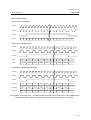
INPUT AND OUTPUT TIMINGS
Data Output Timing
tclkx1
CLKSEL:H
CLKSEL:L
tr
tclkx2
tr
tf
tf
CLKX2
tcxd22
tcxd21
tcxd21
tcxd22
CLKX2O
tcxd11
tcxd11
tcxd21
tcxd21
CLKXO
Tod21
Tod11
Y[9:0],C[9:0],
G[7:0],B[7:0],
R[7:0]
HVALID, VVALID,
HSYNC_L,
VSYNC_L,
ODD/EVEN
STATUS[2:1],
SCALEW ,
SCALER
Tod2x11
Tod2x21
Todx11
Todx21
Tod12
Tod22
Tod2x12
Tod2x22
Todx12
Todx22
Tod13
Tod23
Tod2x13
Tod2x23
Todx13
Todx23
Reset Timing
VDD
POEWR
OFF
GND
CLKX2
ON
Please confirm the data sheet of the clock oscillator that uses it.
Set up Time
Valid Clock
rst_w
RESET L
Don’t Care
The input terminal at the time of the reset is uncertain.
21/36
FEDL86V7666-01
OKI Semiconductor
ML86V7666
I2C-bus Interface Timing
SDA
MSB
ACKA
SCL
1
S
2
7
8
9
ACK
Start Condition
Data Line Stable: Data Valid
1
tC_SCL
2
3-8
9
ACK
P
Stop Condition
Change of Data Allowed
I2C-bus Timing
SDA
BFU
SCL P
tR
tF
tHD:STA
S
S
P
tHD:STA
tLOW
Symbol
fSCL
tBUF
tHD:STA
tLOW
tHIGH
tSU:STA
tHD:DAT
tSU:DAT
tR
tF
tSU:STO
tHD:DAT
tHIGH
tSU:DAT
tSU:STA
Parameter
SCL frequency
Bus open time
Start condition hold time
Clock LOW period
Clock HIGH period
Start condition setup time
Data hold time
Data setup time
Line rise time
Line fall time
Stop condition setup time
tSU:STO
Min.
0
4.7
4.0
4.7
4.0
4.7
300
250
Typ.
100
Max.
400
1
300
4.7
Unit
KHz
µs
µs
µs
µs
µs
ns
ns
µs
ns
µs
The I2C-bus timing is based on the table above.
22/36
FEDL86V7666-01
OKI Semiconductor
ML86V7666
Sync Signal Input and Output Timings (Default)
The following illustrations show the timing of vertical sync signals. The sync signal is output after approximately
1.5H.
524
525
1
2
3
4
5
6
7
8
262
263
264
265
266
267
268
269
270
271
9
21
22
284
285
23
24
337
338
CVBS
HVALID
HSYNC_L
VSYNC_L
CSYNC_L
VVALID
ODD
283
CVBS
HVALID
HSYNC_L
VSYNC_L
CSYNC_L
VVALID
ODD
Vertical Sync Signals (60 Hz)
621
622
623
624
625
1
313
314
2
3
315
316
4
5
6
7
317
318
319
336
25
CVBS
HVALID
HSYNC_L
VSYNC_L
CSYNC_L
VVALID
ODD
309
310
311
312
CVBS
HVALID
HSYNC_L
VSYNC_L
CSYNC_L
VVALID
ODD
PAL VSYNC_L : $04/SYDR[6] = ”1” 2.5H , “0” 3H (default)
Vertical Sync Signals (50 Hz)
23/36
FEDL86V7666-01
OKI Semiconductor
ML86V7666
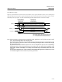
Input/Output Delays (at Standard Signal Input)
The illustration below shows the time delay between the input of a video signal and the output of digital data.
Analog Video In
Data delay
Blank delay
Data output
Blank
Active Data
HSYNC delay
HSYNC_L output
Video mode
NTSC
NTSC
PAL
PAL
NTSC, PAL
NTSC, PAL
Input signal
Composite
Composite
Composite
Composite
S-Video
S-Video
FIFO/FM mode
FIFO-1
FM
FIFO-1
FM
FIFO-1
FM
Delay
about 1.5H
The data delay, blank delay, and sync signal delay are the same length.
Depending on the mode status, the numeric Delay value may vary.
24/36
FEDL86V7666-01
OKI Semiconductor
ML86V7666
Active Pixel Timing
Hsync
Back porch
Front porch
Composite Signal
HSYNC_L
Total pixels
HVALID
60 pixels
Active pixels
H blank
Note: Actually, there is an output delay of about 1H after video signal input.
Total pixels (HSYNC_L)
Active pixels (HVALID)
Total line
(VSYNC L)
Active Field
Active line
(VVALID)
Video Modes and Pixel/Line Counts (at Standard Signal Input)
Video
mode
NTSC
PAL
Sampling
Pixel mode
Output
Pixel rate
(MHz)
Front
porch
ITUR.601
square pixel
4fsc
ITUR.601
square pixel
13.5
12.272727
14.31818
13.5
14.75
16
28
8
12
34
H
Hsync
Active
Back H blank
pixels
porch
122
138
720
112
140
640
134
142
768
132
144
720
142
176
768
V
Total
pixels
858
780
910
864
944
V blank
Active
line
Total
line
odd/20 odd/243 odd/263
even/20 even/242 even/262
odd/23 odd/289 odd/312
even/24 even/289 even/313
Note: Where the FIFO mode is used in asynchronous sampling operations with fixed clock, the 1-field
sampling error accumulated in the line immediately following the fall of VVALID is reset.
Therefore, the pixel count for the line that was reset will change. In addition, where the condition
of VTR and other signals is poor in the FIFO-2 mode, the FIFO reset line might break in before the
fall of VVALID.
25/36
FEDL86V7666-01
OKI Semiconductor
ML86V7666
Sync Signals Output Timing (at Default/Standard Signal Input)
VSYNC_L, ODD/EVEN
60 pixels
HSYNC_L
1/2 H
VSYNC_L
1 pixel
ODD/EVEN
ODD
1 pixel
ODD/EVEN
EVEN
VALID Signal
HSYNC_L
Front porch
HVALID
60 pixels
Back porch
2 pixels
VVALID
0 pixel
26/36
FEDL86V7666-01
OKI Semiconductor
ML86V7666
Output Timing by Mode
10-bit Y/CbCr serial output
CLKX2
CLKXO
HVALID
Y[9:0]
Cr-2 Y-1
Cb0 Y0
Cr0
Y1
Cb2 Y2
Cr2
Crn-3
Yn-2 Cbn-1 Yn-1
Crn-1
Yn
Cbn+1 Yn+1
20-bit Y/CbCr parallel output
CLKX2O
CLKXO
HVALID
Y[9:0]
Y-1
Y0
Y1
Y2
Y3
Yn-1
Yn
C[9:0]
Cr-2
Cb0
Cr0
Cb2
Cr2
Cbn-1
Crn-1
24-bit Y/CbCr and RGB parallel output
CLKX2O
CLKXO
HVALID
Y/G [9:2]
Y-1
Y0
Y1
Y2
Y3
Yn-1
Yn
Cb/B [9:2]
Cb-1
Cb0
Cb1
Cb2
Cb3
Cbn-1
Cbn
Cr/R [9:2]
Cr-1
Cb0
Cr1
Cr2
Cr3
Cbn-1
Crn
Note: Where single-speed (e.g., 13.5 MHz) is input as the input clock in the 16-bit or 24-bit (RGB) output
mode, the waveform of CLKX2 is single-speed, but the format after that is not changed.
27/36
FEDL86V7666-01
OKI Semiconductor
ML86V7666
ITU-R BT.656-4 output:
Output is performed based on BT.656 of the ITU standards. If sync signal information (SAV, EAV) is multiplexed
with video data and the interface complies with BT.656, data can be transferred by connecting to Y data, without
connecting to the sync signal. The data in the blanking period is masked, but the Y data can be output.
Digital line blanking
276T(NTSC 525)
288T(PAL 625)
Multiplexed video data
Cb0 Y0 Cr0 Y1 Cb2 Y2 Cr2 Y3 Cb4 Y4 ------- Cr718 Y719
4T
EAV
4T
SAV
EAV
Y[9:0]
Digital active line
Video data block
1440T(PAL/NTSC)
Digital line
HSYNC_L
Total pixels
HVALID
60 pixels
Active pixels
H blank
EAV: Start of active video timing reference code
SAV: End of active video timing reference code
T:
Clock periods 37ns normal (1/27 MHz)
Note: When operating in the asynchronous sampling mode, digital lines 1716T (NTSC,525) and 1728T
(PAL, 625) will change due to the sampling error.
In the FIFO mode, the pixels count correction function ensures that there is no fluctuation in the
pixel count between active lines, but the line immediately following the fall of VVALID will change
due to the FIFO reset.
In particular, when non-standard signals such as VTR signals are input, the line immediately
following the fall of VVALID will vary greatly in accordance with the degree of the instability of the
input signal. Where the sampling error is large, the line will change immediately before the fall of
VVALID.
In some cases where the line count increases or decreases with respect to the reference, such as
non-standard signals, EAV and SAV may not be guaranteed.
28/36
FEDL86V7666-01
OKI Semiconductor
ML86V7666
INTERNAL REGISTERS
The following is a list of registers. Refer to the User's Manual for details of each register.
Register name
Register bit number
Sub
W/R ADD.
Mode Register A
(MRA)
W/R
Mode Register B
(MRB)
W/R
Mode Register C
(MRC)
W/R
Mode Register D
(MRD)
W/R
Synchronous
Detect Register
(SYDR)
W/R
Not use
W/R
Sync Threshold
Level Adjust
(STHR)
W/R
Horizontal Sync
Delay (HSDL)
W/R
Horizontal Valid
Trimmer (HVALT)
W/R
Vertical Valid
Trimmer (VVALT)
W/R
Luminance
Control (LUMC)
W/R
AGC Loop filter
Control & Lum.
Control Register
(AGCL)
W/R
AGC Reference
Control (AGCRC)
W/R
Contrast Level
Control (CLC)
W/R
00
01
02
03
04
05
Hex
value
Default value
MRA7
MRA6
MRA5
MRA4
MRA3
MRA2
MRA1
MRA0
0
1
0
0
0
0
0
0
MRB7
MRB6
MRB5
MRB4
MRB3
MRB2
MRB1
MRB0
0
0
0
0
0
0
0
0
MRC7
MRC6
MRC5
MRC4
MRC3
MRC2
MRC1
MRC0
1
0
0
0
0
0
0
0
MRD7
MRD6
MRD5
MRD4
MRD3
MRD2
MRD1
MRD0
0
1
0
0
0
0
0
0
40
00
80
40
SYDR7 SYDR6 SYDR5 SYDR4 SYDR3 SYDR2 SYDR1 SYDR0
0
0
0
0
1
0
0
0
-
-
-
-
-
-
-
-
1
1
1
1
0
0
1
0
STHR7
STHR6
STHR5
STHR4
STHR3
STHR2
STHR1
STHR0
0
0
1
0
1
1
0
1
08
F2
06
07
HSDL7 HSDL6 HSDL5 HSDL4 HSDL3 HSDL2 HSDL1
2D
HSDL0
0
0
0
0
0
0
0
0
HVALT7
HVALT6
HVALT5
HVALT4
HVALT3
HVALT2
HVALT1
HVALT0
0
0
0
0
0
0
0
0
VVALT7
VVALT6
VVALT5
VVALT2
VVALT1
VVALT0
0
0
0
0
0
0
00
08
VVALT4 VVALT3
00
09
0A
0
0
00
LUMC7 LUMC6 LUMC5 LUMC4 LUMC3 LUMC2 LUMC1 LUMC0
0
0
0
0
0
0
0
AGCL7 AGCL6 AGCL5 AGCL4 AGCL3 AGCL2 AGCL1
0
00
AGCL0
0B
0
1
0
AGCRC7 AGCRC6 AGCRC5
0
0
0
0
AGCRC4 AGCRC3 AGCRC2 AGCRC1
0
40
AGCRC0
0C
0D
0
0
0
0
0
0
0
0
CLC7
CLC6
CLC5
CLC4
CLC3
CLC2
CLC1
CLC0
1
0
0
0
0
0
0
0
00
80
29/36
FEDL86V7666-01
OKI Semiconductor
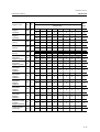
Register name
ML86V7666
Register bit number
Sub
W/R ADD.
Hex
value
Default value
SSEPL7 SSEPL6 SSEPL5 SSEPL4 SSEPL3 SSEPL2 SSEPL1 SSEPL0
Sync Separation
Level (SSEPL)
W/R 0E
Chrominance
Control A
(CHRCA)
W/R 0F
Chrominance
Control B
(CHRCB)
W/R 10
ACC Loop Filter
& Chrominance
Control C
(ACCC)
W/R 11
ACC Reference
Control (ACCRC)
W/R 12
Hue Control
(HUE)
W/R 13
Blue Back &
HDET Control
(BBHC)
W/R 14
Optional Mode
Register A
(OMRA)
W/R 15
Optional Mode
Register B
(OMRB)
W/R 16
Optional Mode
Register C
(OMRC)
W/R 17
Optional Mode
Register D
(OMRD)
W/R 18
Optional Mode
Register E
(OMRE)
W/R 19
Scalar Register
(SCR)
W/R 1A
0
0
0
0
0
0
0
0
00
CHRCA7 CHRCA6 CHRCA5 CHRCA4 CHRCA3 CHRCA2 CHRCA1 CHRCA0
0
0
0
1
0
0
0
0
10
CHRCB7 CHRCB6 CHRCB5 CHRCB4 CHRCB3 CHRCB2 CHRCB1 CHRCB0
0
0
0
0
0
0
0
0
00
ACCC7 ACCC6 ACCC5 ACCC4 ACCC3 ACCC2 ACCC1 ACCC0
0
1
0
0
0
0
0
0
40
ACCRC7 ACCRC6 ACCRC5 ACCRC4 ACCRC3 ACCRC2 ACCRC1 ACCRC0
0
0
0
0
0
0
0
0
HUE7
HUE6
HUE5
HUE4
HUE3
HUE2
HUE1
HUE0
0
0
0
0
0
0
0
0
00
00
BBHC7 BBHC6 BBHC5 BBHC4 BBHC3 BBHC2 BBHC1 BBHC0
1
0
0
1
0
0
0
0
90
OMRA7 OMRA6 OMRA5 OMRA4 OMRA3 OMRA2 OMRA1 OMRA0
1
0
0
0
0
0
0
0
80
OMRB7 OMRB6 OMRB5 OMRB4 OMRB3 OMRB2 OMRB1 OMRB0
0
0
1
0
1
0
1
0
2A
OMRC7 OMRC6 OMRC5 OMRC4 OMRC3 OMRC2 OMRC1 OMRC0
0
1
1
0
1
0
0
0
68
OMRD7 OMRD6 OMRD5 OMRD4 OMRD3 OMRD2 OMRD1 OMRD0
0
0
0
0
0
0
0
0
00
OMRE7 OMRE6 OMRE5 OMRE4 OMRE3 OMRE2 OMRE1 OMRE0
0
0
0
0
0
0
0
0
SCR7
SCR6
SCR5
SCR4
SCR3
SCR2
SCR1
SCR0
0
0
0
0
0
0
0
0
00
00
30/36
FEDL86V7666-01
OKI Semiconductor
Register name
ML86V7666
Scalar V-Position
Register
(SCVPR)
W/R
Scalar H-Position
Register
(SCHPR)
W/R
ADC Register 1
(ADC1)
W/R
ADC Register 2
(ADC2)
W/R
PLL Resister
(PLLR)
W/R
Closed Caption
Detected-1
Register (CCD1)
Closed Caption
Detected-2
Register (CCD2)
CGMS
Detected-1
Register
(CGMS1)
CGMS
Detected-2
Register
(CGMS2)
AGC pulse
Detected-1
Register
(AGCD1)
AGC pulse
Detected-2
Register
(AGCD2)
0WSS data
Detected-1
Register
(WSSD1)
Reset data
Request for VBID
Function
Register (AIREG)
Status Register
(STATUS)
Register bit number
Sub
W/R ADD.
Hex
value
Default value
SCVPR7 SCVPR6 SCVPR5 SCVPR4 SCVPR3 SCVPR2 SCVPR1 SCVPR0
1B
0
0
0
0
0
0
0
0
00
SCHPR7 SCHPR6 SCHPR5 SCHPR4 SCHPR3 SCHPR2 SCHPR1 SCHPR0
1C
0
1D
20
21
0
0
0
00
0
0
0
0
0
0
0
00
0
0
1
0
0
0
0
0
0
0
1
91
PLLR2 PLLR1 PLLR0
0
0
0
00
CCD17 CCD16 CCD15 CCD14 CCD13 CCD12 CCD11 CCD10
0
W/R
0
PLLR7 PLLR6 PLLR5 PLLR4 PLLR3
0
W/R
0
ADC27 ADC26 ADC25 ADC24 ADC23 ADC22 ADC21 ADC20
1
1F
0
ADC17 ADC16 ADC15 ADC14 ADC13 ADC12 ADC11 ADC10
0
1E
0
0
0
0
0
0
0
0
00
CCD27 CCD26 CCD25 CCD24 CCD23 CCD22 CCD21 CCD20
0
0
0
0
0
0
0
0
00
CGMS17 CGMS16 CGMS15 CGMS14 CGMS13 CGMS12 CGMS11 CGMS10
W/R
22
0
0
0
0
0
0
0
0
00
CGMS27 CGMS26 CGMS25 CGMS24 CGMS23 CGMS22 CGMS21 CGMS20
W/R
23
0
0
0
0
0
0
0
0
00
AGCD17 AGCD16 AGCD15 AGCD14 AGCD13 AGCD12 AGCD11 AGCD10
W/R
24
0
0
0
0
0
0
0
0
00
AGCD27 AGCD26 AGCD25 AGCD24 AGCD23 AGCD22 AGCD21 AGCD20
W/R
25
0
0
0
0
0
0
0
0
00
WSSD7 WSSD6 WSSD5 WSSD4 WSSD3 WSSD2 WSSD1 WSSD0
W/R
26
0
0
0
0
0
0
0
0
00
AIREG7 AIREG6 AIREG5 AIREG4 AIREG3 AIREG2 AIREG1 AIREG0
W/R
27
0
0
0
0
0
0
0
0
00
STATUS7 STATUS6 STATUS5 STATUS4 STATUS3 STATUS2 STATUS1 STATUS0
Read
28
—
—
—
—
—
—
—
—
31/36
FEDL86V7666-01
OKI Semiconductor
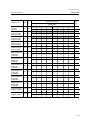
Register name
ML86V7666
Register bit number
Sub
Hex
value
W/R ADD.
Default value
VBID Flag
Register
(VFLAG)
C.C. Data Buffer
Register in Odd
Field (CCDO0)
C.C. Data Buffer
Register in Odd
Field (CCDO1)
C.C. Data Buffer
Register in Even
Field (CCDE0)
C.C. Data Buffer
Register in Even
Field (CCDE1)
CGMS Data
Buffer Register in
Odd Field
(CGMSO0)
CGMS Data
Buffer Register in
Odd Field
(CGMSO1)
CGMS Data
Buffer Register in
Odd Field
(CGMSO2)
CGMS Data
Buffer Register in
Even Field
(CGMSE0)
CGMS Data
Buffer Register in
Even Field
(CGMSE1)
CGMS Data
Buffer Register in
Even Field
(CGMSE2)
VFLAG7 VFLAG6 VFLAG5 VFLAG4 VFLAG3 VFLAG2 VFLAG1 VFLAG0
Read
29
—
—
—
—
—
—
—
—
CCDO07 CCDO06 CCDO05 CCDO04 CCDO03 CCDO02 CCDO01 CCDO00
Read
2A
—
—
—
—
—
—
—
—
CCDO17 CCDO16 CCDO15 CCDO14 CCDO13 CCDO12 CCDO11 CCDO10
Read
2B
—
—
—
—
—
—
—
—
CCDE07 CCDE06 CCDE05 CCDE04 CCDE03 CCDE02 CCDE01 CCDE00
Read
2C
—
—
—
—
—
—
—
—
CCDE17 CCDE16 CCDE15 CCDE14 CCDE13 CCDE12 CCDE11 CCDE10
Read
2D
—
—
—
—
—
—
—
—
CGMSO07 CGMSO06CGMSO05 CGMSO04 CGMSO03 CGMSO02 CGMSO01 CGMSO00
Read
2E
—
—
—
—
—
—
—
—
CGMSO17 CGMSO16CGMSO15 CGMSO14 CGMSO13 CGMSO12 CGMSO11 CGMSO10
Read
2F
—
—
—
—
—
—
—
—
CGMSO27 CGMSO26CGMSO25 CGMSO24 CGMSO23 CGMSO22 CGMSO21 CGMSO20
Read
30
—
—
—
—
—
—
—
—
CGMSE07 CGMSE06 CGMSE05 CGMSE04 CGMSE03 CGMSE02 CGMSE01 CGMSE00
Read
31
—
—
—
—
—
—
—
—
CGMSE17 CGMSE16 CGMSE15 CGMSE14 CGMSE13 CGMSE12 CGMSE11 CGMSE10
Read
32
—
—
—
—
—
—
—
—
CGMSE27 CGMSE26 CGMSE25 CGMSE24 CGMSE23 CGMSE22 CGMSE21 CGMSE20
Read
33
—
WSS Data Buffer
Read
Register (WSS0)
34
WSS Data Buffer
Read
Register (WSS1)
35
—
—
—
—
—
—
—
WSS07 WSS06 WSS05 WSS04 WSS03 WSS02 WSS01 WSS00
—
—
—
—
—
—
—
—
WSS17 WSS16 WSS15 WSS14 WSS13 WSS12 WSS11 WSS10
—
—
—
—
—
—
—
—
32/36
FEDL86V7666-01
OKI Semiconductor
ML86V7666
NOTES ON USE
The ML86V7666 Video Decoder is being developed based on standard signals. Improvements are being made to
ensure stable operation even with non-standard signals. However, the signal conditions and usage environments
differ widely for signals such as those having a weak electromagnetic field, VTR playback signals, signals with
numerous signal switching or a large amount of noise, and simple video signals from various cameras. As a result,
stable operation for all signals has not yet been confirmed. Before using the decoder, please carefully evaluate and
consider the signal conditions and usage environment of the intended use.
In addition to this Data Sheet, a ML86V7666 User's Manual is also available. The User's Manual explains each
register and provides examples of adapted circuits as well as other information helpful in the design phase. Please
read the User's Manual before embarking on design work.
Users are also requested to regularly download the most recent versions of this Data Sheet and the User's Manual
from the Oki web site. As the newest information, not included in printed materials, and the answers to frequently
asked questions are published on the web site, users are recommended to check the site regularly for updates.
33/36
FEDL86V7666-01
OKI Semiconductor
ML86V7666
PACKAGE DIMENSIONS
(Unit: mm)
TQFP100-P-1414-0.50-K
Mirror finish
5
Package material
Lead frame material
Pin treatment
Package weight (g)
Rev. No./Last Revised
Epoxy resin
42 alloy
Solder plating (≥5µm)
0.55 TYP.
4/Oct. 28, 1996
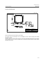
Notes for Mounting the Surface Mount Type Package
The surface mount type packages are very susceptible to heat in reflow mounting and humidity
absorbed in storage.
Therefore, before you perform reflow mounting, contact Oki’s responsible sales person for the product
name, package name, pin number, package code, and desired mounting conditions (reflow method,
temperature and times).
34/36
FEDL86V7666-01
OKI Semiconductor
ML86V7666
REVISION HISTORY
Document
No.
Date
Page
Previous Current
Edition
Edition
Description
Version 1
Oct. 30, 2002
–
–
Preliminary edition 1
Version 2
Jun. 5. 2003
–
–
Preliminary edition 2
Version 3
Apr. 9. 2004
36
36
Preliminary edition 3
FEDL86V7666-01
Apr. 20. 2004
36
36
Final edition 1
35/36
FEDL86V7666-01
OKI Semiconductor
ML86V7666
NOTICE
1. The information contained herein can change without notice owing to product and/or technical improvements.
Before using the product, please make sure that the information being referred to is up-to-date.
2.
The outline of action and examples for application circuits described herein have been chosen as an
explanation for the standard action and performance of the product. When planning to use the product, please
ensure that the external conditions are reflected in the actual circuit, assembly, and program designs.
3.
When designing your product, please use our product below the specified maximum ratings and within the
specified operating ranges including, but not limited to, operating voltage, power dissipation, and operating
temperature.
4.
Oki assumes no responsibility or liability whatsoever for any failure or unusual or unexpected operation
resulting from misuse, neglect, improper installation, repair, alteration or accident, improper handling, or
unusual physical or electrical stress including, but not limited to, exposure to parameters beyond the specified
maximum ratings or operation outside the specified operating range.
5.
Neither indemnity against nor license of a third party’s industrial and intellectual property right, etc. is
granted by us in connection with the use of the product and/or the information and drawings contained herein.
No responsibility is assumed by us for any infringement of a third party’s right which may result from the use
thereof.
6.
The products listed in this document are intended for use in general electronics equipment for commercial
applications (e.g., office automation, communication equipment, measurement equipment, consumer
electronics, etc.). These products are not, unless specifically authorized by Oki, authorized for use in any
system or application that requires special or enhanced quality and reliability characteristics nor in any
system or application where the failure of such system or application may result in the loss or damage of
property, or death or injury to humans.
Such applications include, but are not limited to, traffic and automotive equipment, safety devices, aerospace
equipment, nuclear power control, medical equipment, and life-support systems.
7.
Certain products in this document may need government approval before they can be exported to particular
countries. The purchaser assumes the responsibility of determining the legality of export of these products
and will take appropriate and necessary steps at their own expense for these.
8.
No part of the contents contained herein may be reprinted or reproduced without our prior permission.
Copyright 2004 Oki Electric Industry Co., Ltd.
36/36