1
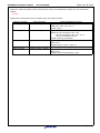
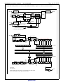
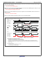
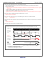
RENESAS TECHNICAL UPDATE TN-16C-A239A/E
Date: Jan. 28, 2015
RENESAS TECHNICAL UPDATE
1753, Shimonumabe, Nakahara-ku, Kawasaki-shi, Kanagawa 211-8668 Japan
Renesas Electronics Corporation
Product
Category
Title
MPU & MCU
Document
No.
Deletion of Specifications and Errata for R32C/
117A Group User’s Manual: Hardware
Information
Technical Notification
Category
TN-16C-A239A/E
Rev. 1.00
Lot No.
Applicable
R32C/117A Group
Product
Reference
Document
R32C/117A Group User’s Manual:
Hardware Rev. 1.10
(R01UH0214EJ0110)
This document describes deletion of specifications and errata for the R32C/117A Group User’s Manual:
Hardware, Rev. 1.10.
1.
Deletion of Specifications
Development of products on the planning phase in Table 1.5 is discontinued. Accordingly, specifications for the N
version are deleted from the Operating Temperature in Tables 1.2, 1.4, and 29.2, and the Temperature Code in
Figure 1.1.
2.
Errata
The corrections are indicated in red in the list below.
• Page 1 of 625, expression “I2C” in line 9 of 1.1 is modified as follows:
“I2C-bus interface”
• Page 171 of 625, description in lines 9 and 10 of chapter 12 is modified as follows:
“One divides the on-chip oscillator clock by 1, 2, 4 or 8; the other divides the peripheral bus clock by 16 or
128.”
• Page 198 of 625, descriptions in Figure 14.5 is modified as follows:
“The figure below applies under the following conditions:
memory-to-memory transfer; incrementing source address; non-incrementing destination address; single
transfer mode; transfer complete interrupt generated after 2 transfers (transfer counter = 2); no chain
transfer”
• Page 205 of 625, description of the third bullet point of 16.1 is corrected as follows:
“One-shot timer mode: The timer outputs a pulse after a trigger input until the counter reaches 0000h”
• Page 210 of 625, typos “b2 b3”, “b4 b5”, and “b6 b7” in Figure 16.9 are corrected as follows:
“b3 b2”, “b5 b4”, and “b7 b6”
• Page 217 of 625, typo “INT” in Note 1 of Figures 16.13 and 16.14 is corrected as follows:
“INT2”
©2015. Renesas Electronics Corporation, All rights reserved.
Page 1 of 9
RENESAS TECHNICAL UPDATE
Date: Jan. 28, 2015
TN-16C-A239A/E
• Page 221 of 625, bit symbol “TAiS” in the Function column for the MR2 bit in Figure 16.16 is corrected as
follows:
“TAiOS”
• Pages 254 to 305 of 625, terms in chapter 18 are corrected as follows:
Before Correction
receive register
After Correction
receive shift register
transmit register
transmit shift register
SS function
slave select function
BRG
restart condition
UiBRG
repeated START condition
Figure/Table/Section Number
Figures 18.1, 18.2, 18.22, 18.28
Tables 18.2, 18.5, 18.11, 18.14
Section 18.3.8
Figures 18.1, 18.2, 18.21, 18.22, 18.26, 18.27
Tables 18.2 (2 corrections), 18.3, 18.4,
18.5 (2 corrections), 18.6, 18.7, 18.10,
18.14 (2 corrections), 18.15
Section 18.3.8 (3 corrections)
Figure 18.13 (3 corrections)
Table 18.14
Sections 18.4.1, 18.4.1.1, 18.4.1.2
Table 18.8 (3 corrections)
Figure 18.14
Table 18.10
Sections 18.3.2 (2 corrections), 18.5.3
Page 2 of 9
RENESAS TECHNICAL UPDATE
Date: Jan. 28, 2015
TN-16C-A239A/E
• Page 255 of 625, positions of “010” for bits SMD2 to SMD0 in Figure 18.1 are corrected as follows:
RXD polarity
switch circuit
RXDi
SMD2 to SMD0
CLK1 and CLK0
00
CKDIR UiBRG
f1
register
01
0
1/16
1/(m+1)
1/16
f8
10
f2n
1
100, 101, 110
001, 010
Receive
clock
Transmit/
Receive control
receive
circuit
TXD polarity
switch circuit
TXDi
unit
100, 101, 110
Transmit control
circuit
001, 010
CKDIR
Transmit
clock
0
1/2
1
CKPOL
CLK polarity
switch circuit
CLKi
CKDIR
Direction register
CTSi/RTSi
RTSi
CTSi
CRD
m: Value set in the UiBRG register
IOPOL
0
1
RXDi
SMD2 to SMD0
STPS
SP
0
1
PRYE
SP
001,
010
001,
101
0
PAR 1
b8
100,
101,
110
0
0
0
0
0
0
b6
b5
b4
b3
b2
b1
b0
D6
D5
D4
D3
D2
D1
D0
001,
010,
101,
110
010,
110
0
UARTi receive shift register
100
b7
D8
D7
UiRB register
Logic inversion circuit + Bit order reverse circuit
Upper byte of data bus
Lower byte of data bus
Logic inversion circuit + Bit order reverse circuit
D8
STPS
SP
SP
0
1
PRYE
001,
010
0
PAR 1
D7
001,
101
b8
100,
101,
110
D6
D5
D4
D3
D2
D1
D0
b6
b5
b4
b3
b2
b1
b0
UiTB register
100
b7
010,
110
SMD2 to SMD0
SP: Stop bit
PAR: Parity bit
001,
010,
101,
110
UARTi transmit shift register
IOPOL
0
1
TXDi
SMD2 to SMD0, STPS, PRYE, IOPOL, and CKDIR: Bits in the UiMR register
CLK1, CLK0, CKPOL, and CRD: Bits in the UiC0 register
Page 3 of 9
RENESAS TECHNICAL UPDATE
Date: Jan. 28, 2015
TN-16C-A239A/E
• Page 265 of 625, expression “baud rate generator count source” in the function of bits DL0 to DL2 in Figure
18.13 is corrected as follows:
“count source for the UiBRG register”
• Pages 272, 273, 280, 281, 290, 300 of 625, descriptions in Function of the UiBRG register in Tables 18.3, 18.4,
18.6, 18.7, 18.10, and 18.15 are modified as follows:
“Set the divide ratio according to the bit rate”
• Pages 273, 281 of 625, description for (b7 to b4) to registers UiC1 and U78CON in Tables 18.4 and 18.7 is
added as follows:
“(b7 to b4) Set the bits to 0000b”
• Page 274 of 625, waveform of the IR bit in Figure 18.21 is corrected as follows:
Transmit timing (when selecting an internal clock)
Internal
transmit/receive
clock
TE bit in the
UiC1 register
TC
Data is set to the UiTB register
Data is transferred from the UiTB register
to the UARTi transmit shift register
TI bit in the
UiC1 register
CTSi
TCLK
Pulse stops because the input
level at the CTSi pin is high
Pulse stops because the TE bit is set to 0
CLKi
TXDi
D0 D1 D2 D3 D4 D5 D6
D7
D0 D1 D2 D3 D4 D5 D6
D7
D0 D1 D2 D3 D4 D5 D6 D7
TXEPT bit in the
UiC0 register
IR bit in the
SiTIC register
Set to 0 by accepting an interrupt or by a program
This figure applies under the following conditions:
- The CKDIR bit in the UiMR register is 0 (internal clock).
- The CRD bit in the UiC0 register is 0 (CTS function enabled).
- The CKPOL bit in the UiC0 register is 0 (output transmit data on the falling edge of the transmit/receive clock).
- The UiIRS bit in registers UiC1, U78CON, and U910CON is 0 (an interrupt request is generated when the transmit
buffer is empty).
TC = TCLK = 2(m + 1)/fx
fx: UiBRG count source frequency (f1, f8, or f2n)
m: Value setting in the UiBRG register
Page 4 of 9
RENESAS TECHNICAL UPDATE
Date: Jan. 28, 2015
TN-16C-A239A/E
• Page 276 of 625, descriptions in 18.1.1 are modified as follows:
“When a transmit/receive error occurs in synchronous serial interface mode, follow the procedures
below to perform a reset:
(1) Set the TE bit to 0 (transmission disabled) and the RE bit to 0 (reception disabled) in the UiC1 register
(i = 0 to 10).
(2) Set bits SMD2 to SMD0 in the UiMR register to 000b (serial interface disabled).
(3) Set again bits SMD2 to SMD0 to either of 001b, 101b, or 110b.
(4) Set the TE bit to 1 (transmission enabled) and the RE bit to 1 (reception enabled) in the UiC1 register.”
• Page 278 of 625, the following description is added to line 3 of 18.1.6:
“after the last bit is transmitted”
• Page 281 of 625, description for (b7) to the UiMR register in Table 18.7 is added as follows:
“(b7)
Set the bit to 0”
• Pages 282, 283 of 625, description “Internal transmit/receive clock” in Figures 18.26 and 18.27 is corrected as
follows:
“Internal transmit clock”
• Page 284 of 625, Figure 18.28 is corrected as follows:
Example of data receive timing when the character length is 8-bit (parity disabled, 1 stop bit)
UiBRG output
RE bit in the
UiC1 register
RXDi
Start bit
D0
D1
D7
Stop bit
Data reception starts when the receive clock is
generated on the falling edge of the start bit
Internal
receive clock
Low is reverified
RI bit in the
UiC1 register
Input of receive data
Data is transferred from the UARTi receive shift register to the UiRB register
The UiRB register is read
RTSi
It becomes low when the UiRB register is read
IR bit in the
SiRIC register
Set to 0 by accepting an interrupt request or by a program
This figure applies under the following conditions:
- The PRYE bit in the UiMR register is 0 (parity disabled).
- The STPS bit in the UiMR register is 0 (1 stop bit).
Page 5 of 9
RENESAS TECHNICAL UPDATE
TN-16C-A239A/E
Date: Jan. 28, 2015
• Page 285 of 625, descriptions in 18.2.2 are modified as follows:
“When a transmit/receive error occurs in UART mode, follow the procedure below to perform a reset:
(1) Set the TE bit to 0 (transmission disabled) and the RE bit to 0 (reception disabled) in the UiC1 register
(i = 0 to 10).
(2) Set bits SMD2 to SMD0 in the UiMR register to 000b (serial interface disabled).
(3) Set again bits SMD2 to SMD0 to either of 001b, 101b, or 110b.
(4) Set the TE bit to 1 (transmission enabled) and the RE bit to 1 (reception enabled) in the UiC1 register.
• Page 288 of 625, descriptions for the Interrupt request generating timing in Table 18.9 are modified as follows:
Interrupt request generating
timing
• START condition is detected
• STOP condition is detected
• ACK (acknowledge) is detected, or reception is completed
• NACK (not-acknowledge) is detected, or transmission is completed
• Page 290 of 625, description for (b6 to b4) to the UiMR register in Table 18.10 is added as follows:
“(b6 to b4) Set the bits to 000b”
• Page 305 of 625, description for suspending and resuming communication is added to 18.5.4 as follows:
“18.5.4 Reset Procedure or Suspend/Resume Procedure
Operations which result in communication errors such as rewriting function select registers during
transmission/reception should not be performed. Follow the procedure below to reset the internal circuit
once the communication error occurs in the following cases: when the operation above is performed by
a receiver or transmitter or when a bit slip is caused by noise.
Also follow the procedure below when suspending and resuming communication in an emergency.”
• Page 418 of 625, description for Mode transition for bus-off recovery in Table 26.1 is modified as follows:
Mode transition for
bus-off recovery
Mode after recovering from the bus-off state can be selected:
• ISO 11898-1 compliant
• Automatic transition to CAN halt mode immediately after becoming bus-off.
• Automatic transition to CAN halt mode when recovering from the bus-off state.
• Transition to CAN halt mode by a program
• Transition to the error-active state by a program
• Page 419 of 625, description for Mode transition for Error state monitoring in Table 26.2 is modified as follows:
Error state monitoring
• CAN bus errors (stuff error, form error, ACK error, CRC error, bit error, and ACK
delimiter error) can be monitored
• Transition to error states can be detected (error-warning, error-passive, bus-off,
and bus-off recovery)
• The error counters can be read
• Page 422 of 625, description for the BOM bit in Figure 26.2 is modified as follows:
“00: Normal mode
(ISO 11898-1 compliant)
01: Automatically enters CAN halt mode immediately after becoming bus-off
10: Automatically enters CAN halt mode when recovering from the bus-off state
11: Enters CAN halt mode (during bus-off period) by a program request”
Page 6 of 9
RENESAS TECHNICAL UPDATE
Date: Jan. 28, 2015
TN-16C-A239A/E
• Page 426 of 625, the following description is added to 26.1.2:
“The C0CLKR register is used to select the clock source of the CAN communication clock for the protocol
controller. Operation in the CAN module is always synchronized with the peripheral bus clock.”
• Page 429 of 625, description in 26.1.4 is modified as follows:
“Each channel has eight mask registers. Refer to 26.5 “Acceptance Filtering and Masking Function” for details
on the mask registers.”
• Page 433 of 625, description is added to 26.1.7 as follows:
“Each channel has 32 mailboxes. Each mailbox is 16 bytes and can be set for transmission or for reception
individually by the C0MCTLj register.
Table 26.4 lists the CAN0 mailbox memory mapping, and Table 26.5 lists the CAN data frame structure.
The reset value of the CAN0 mailbox is undefined.”
• Page 454 of 625, register symbol “CiMSSR” in the Function column of Figure 26.20 is corrected as follows:
“C0MSSR”
• Page 458 of 625, descriptions for bits BOEIF and BORIF are modified in Figure 26.25 as follows:
Bit Symbol
BOEIF
BORIF
Bit Name
Bus-off Detect Flag
Function
0:CAN module is not bus-off
1:CAN module became bus-off
RW
RW
Bus-off Recovery Detect Flag 0:CAN module does not recover from the bus-off state
RW
1:CAN module recovered from the bus-off state normally
• Page 460 of 625, description in 26.1.20.8 is corrected as follows (refer to TN-16C-A230A/E):
“The BLIF bit becomes 1 if 32 consecutive dominant bits are detected on the CAN bus while the CAN
module is in CAN operation mode.
After the BLIF bit becomes 1, bus lock can be detected again after either of the following conditions is
satisfied:
•After this bit is set to 0 from 1, recessive bits are detected (bus lock is resolved).
•After this bit is set to 0 from 1, the CAN module enters CAN reset mode and then enters CAN operation
mode again (internal reset).”
• Page 469 of 625, Note 1 in Figure 26.34 is corrected and Note 3 is added as follows (refer to TN-16C-A230A/
E):
“Notes:
1. The transition timing from the bus-off state to CAN halt mode depends on the setting of the BOM bit.
- When the BOM bit is 01b, the CAN module enters CAN Halt mode immediately after becoming bus-off.
- When the BOM bit is 10b, the CAN module enters CAN Halt mode when recovering from the bus-off state.
- When the BOM bit is 11b, the CAN module enters CAN Halt mode when setting the CANM bit to 10b (CAN
halt mode).
2. Write only to the SLPM bit to exit/set CAN sleep mode.
3. The CAN module does not enter CAN Halt mode while the CAN bus is locked in dominant state. Enter CAN
reset mode instead.”
Page 7 of 9
RENESAS TECHNICAL UPDATE
TN-16C-A239A/E
Date: Jan. 28, 2015
• Page 471 of 625, Note 2 is added to the CAN halt mode row in the Transmitter column of Table 26.9.
Note 2, Note 3, and Note 4 is corrected as follows (refer to TN-16C-A230A/E):
Notes:
1. If several messages are requested to be transmitted, mode transition occurs after the completion of
the first message transmission. When CAN reset mode is being requested during suspend
transmission, mode transition occurs when the bus is idle, the next transmission ends, or the CAN
module becomes a receiver.
2. If the CAN bus is locked in dominant state, the program can detect this state by monitoring the BLIF
bit in the C0EIFR register. The CAN module does not enter CAN Halt mode while the CAN bus is
locked in dominant state. Enter CAN reset mode instead.
3. If a CAN bus error occurs during reception after CAN halt mode is requested, the CAN module
enters CAN halt mode. However, the CAN module does not enter CAN Halt mode when the CAN bus
is locked in dominant state.
4. If a CAN bus error or arbitration lost occurs during transmission after CAN reset mode or CAN halt
mode is requested, the CAN module enters the requested operating mode. However, the CAN
module does not enter CAN Halt mode when the CAN bus is locked in dominant state.
• Page 472 of 625, register symbol “CiCTLR” in line 7 of 26.2.3 is corrected as follows:
“C0CTLR”
• Page 485 of 625, bit symbol “SENDTDATA” in (4) of 26.6.2 is corrected as follows:
“SENTDATA”
• Page 487 of 625, descriptions in lines 5 and 6 of 27. I/O Pins are modified as follows:
“The pull-up resistors are enabled for every group of four pins. However, when a pin functions as an output
pin, a pull-up resistor is disabled regardless of the register settings.”
• Page 487 of 625, description in the last paragraph of 27. I/O Pins is corrected as follows:
“The input-only port P8_5 shares a pin with NMI and has neither function select register nor the
corresponding direction bit. Port P14_1 also functions as an input-only port. The function select register and
bit 1 in the PD14 register are reserved. Port P9 is protected from unexpected write accesses by the PRC2
bit in the PRCR register (refer to 10. “Protection”).”
• Pages 521, 522 of 625, description in Note 2 of Tables 27.2 and 27.3 are modified as follows:
“When configuring as an output port to release the pin open, it remains as an input port until it is set as an
output port after a reset is released. Therefore, while it remains as an input port, the power supply current
may increase due to the undefined voltage level of the pin. In addition, the direction register value may
change due to noise or program runaway caused by the noise. To avoid these situations, reconfigure the
direction register regularly by software, which may achieve higher program reliability.”
• Pages 521, 522 of 625, description “addresses: 03E2h, 03E3h, 03E6h and 03E7h” in Note 4 of Tables 27.2
and 27.3 is modified as follows:
“registers PD16 and PD17, PD18, and PD19”
• Page 581, 584, 594, 597, 614 of 625, expression “restart condition” in Tables 29.34, 29.39, 29.40, 29.60,
29.65, 29.66, and line 1 of 30.9.3 is modified as follows:
“repeated START condition”
Page 8 of 9
RENESAS TECHNICAL UPDATE
TN-16C-A239A/E
Date: Jan. 28, 2015
• Page 615 of 625, description for suspending and resuming communication is added to 30.9.4 as follows:
“30.9.4 Reset Procedure or Suspend/Resume Procedure
Operations which result in communication errors such as rewriting function select registers during
transmission/reception should not be performed. Follow the procedure below to reset the internal circuit
once the communication error occurs in the following cases: when the operation above is performed by
a receiver or transmitter or when a bit slip is caused by noise.
Also follow the procedure below when suspending and resuming communication in an emergency.”
Page 9 of 9