1
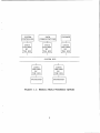
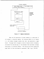
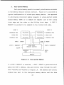
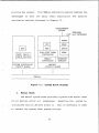
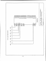
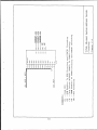
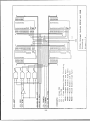
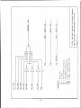
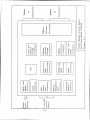
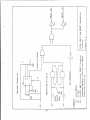
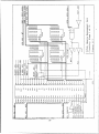
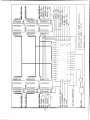
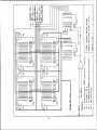
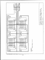
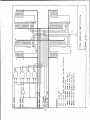
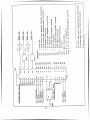
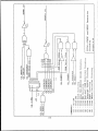
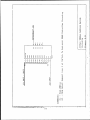
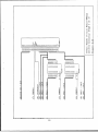
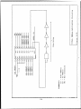
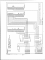
$7F7010 through $7F7FFF are multiple maps for the DUART.
maps provide valid addresses to chip select the DUART.
permit address decoding logic to be simplified.
Multiple
They also
However, to avoid
ambiguity, only the physical addresses $7F7000 through $7F700F are
used to address the DUART.
2.
Hardware Interface
Appendix
minimal system.
C
illustrates
the
circuitry
involved
in
the
Figures C.1 through C.8 illustrate the minimum
system in its entirety.
Figure C.1 illustrates the MC68010 microprocessor used in
the minimal system design.
Figure C.2
circuitry.
illustrates
The NE555 timer provides an automatic system reset when
the system is powered up.
switch
the HALT* and RESET* generation
(push button).
There is also a manual system reset
Resetting
the
system
internal circuitry of the CPU and DUART.
the
reset circuitry
unneeded
buffer.
has
one
in
the
the
A two-input OR gate in
input grounded,
However,
initializes
fully
so
it
acts
integrated
as
an
system
(discussed later in this chapter), this input is tied to the VMEbus
system reset (SYSRESET*) line.
This permits a system-wide reset to
the master circuit board illustrated in Figure 3.1.
Figure C.3 illustrates the clock generation circuitry. The
8 MHz CPU
counter
to
oscillator.
clock signal
divide
a 16
is
MHz
produced by using
signal
from
a 74LS161
a crystal
binary
controlled
A 4 MHz signal from the 74LS161 provides the clock
35