1
NAVAL POSTGRADUATE SCHOOL
Monterey, California
In
DTIC
ELECTE
R AD %
MARO 6 1991n
THESIS
DESIGNING A VIRTUAL-MEMORY IMPLEMENTATION USING THE
MOTOROLA MC68010 16-BIT MICROPROCESSOR WITH
MULTI-PROCESSOR CAPABILITY INTERFACED TO THE VMEbus
by
David M. Sendek
June 1990
Thesis Advisor:
Larry W. Abbott
Approved for public release; distribution is unlimited.
91 3
04 004
Unclassified
SECLR -V CLASS,'C,7
O
O; -1 S PAGE
Form Appro ed
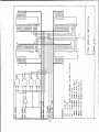
REPORT DOCUMENTATION PAGE
1t
RESTR:CTVE
3
DSTR Bf.ON.
REPORT SECdRTY CASSW CAThON
la
OmBNo 004o0188
MARr
NGS
UNCLASSTFTED
2a SECURI'Y CLASS'
CA- ON A,7OR _'y
20 DECLASSIriCAThON
4 PERFORMANG ORGAVZAT ON REPORT NuMBERIS)
5 Mor
7a
6b OFF CE SYMBOL
(If applicable)
Naval Postgraduate School
EC
California
7D
93943-5000
'
ORING ORGAN ZATON REPORT %,
,ZSEa.S
NAME Of
RNG ORGAN ZAON
.
'0
S7'-_CE
'
OPA
C_4V
L
and ZIP Cooe)
ADDRESS (CityState
California
9 PROCuREMEV
ADDRESS (City State, and ZIPCode)
8,
T
Monterey,
Mv% D
8bT O
8:
(if apphcahle)
E Or
NDNG SPONSOR
8a N
ORGANiZATION
OF RE0P
Naval Postgraduate School
6c ADDRESS (City State. and ZIP Code)
Monterey,
.T
Approved for public release;
distribution is unlimited.
DOVL'NGRAD NC SCHEDULE
6a NAME OF PERFORMANG ORGAN ZATiON
AVA LAB J
MEN'
NO
NS'R.;ENT
F.ND
93943-5000
DEN% ; CA--ON' N .SEP
"'.X
BEPS
N
OE
0, CT
%C
NO
~2O
ACCESSON NO
A VIRTUAL-MEMORY IMPLEMENTATION USING THE MOTOROLA
1 TITLE (Include Security Classficaton) DESIGNING
MC68010 16-BIT MICROPROCESSOR WITH MULTI-PROCESSOR CAPABILITY INTERFACED TO THE
0
PE PNA_ A-THOR(S)
2
13a
-Y;E O
Sendek. David. M.
REPORT
3t, T.ME COVERED
R0,
Mdster's Thesis
16 SUPP.EENAP
not reflect
Cnvornmont_
ELD
19 ABS
(Y'ar, Month Day)
P7
1990
1 175
The views expressed in this thesis are those of the author and do
NOTATOA.
the official policy or position of the Department of Defense or the U.S.
18 S.B....T TERMS
COSA '! CODtS
7
4 DATE OF REPORT
TOJune
GrouP
SS-GcO-P
Continue on reverse if necessary and identify by block number)
MC68010 Microprocessor, VMEbus,
Memory, Multi-processor
Virtual-Memory,
Dual-port
.;ACT (Continue on reverse if necessary and identify by block number)
The primary purpose of this thesis is to explore and discuss the hardware design of
a bus-oriented microprocessor system. A bus-oriented microprocessor system permits it to
be expanded to a multi-processor system. Through the use of a bus controller and bus
arbiter, as discussed in this thesis, the necessary logic is in place to control bus
access by system users. Bus access may be initiated to share another sub-system's
resource, such as memory. To accommodate memory sharing between two systems, a dual-port
memory controller can be used to resolve memory access between the two systems. This
thesis discusses the design of a MC68010 microprocessor system integrated on the VMEbus
with dual-ported memory capability. Additional features of the MC68010 microprocessor
system include memory-management and interrupt control. The memory-management features
permit protected memory and virtual-memory to be implemented on the system, while an
interrupt handler is used to assist the MC68010 microprocessor in exception processing.
DSTFR:'iON
F
,'
[
~
AM
21
'y 0) ABS'RA(
AvA.LA
JN.CL/SS~F 'ED iN I'MI ED
'
SAME AS
ES~SR.
*
'"
'
,C
LJSES
~ ~22b
C
(A- O%
9;."
71 3-48'-S93
Larry W. Abbott
DD Form 1473. JUN 86
ABSRACT SECJR 'V C, ASS
T1nr 1 nQc i f'i -,
'E.E Pr'ON (Incude Area tode(
Prev(,Lus edtions are obsolete
S/N 1] (2-1,-0 1
i
SEE ''
3Uc
(A N F A
lassi fied
.I)
EC/AT
('N
"
Pi
Approved for public release; distribution is unlimited.
DESIGNING A VIRTUAL-MEMORY IMPLEMENTATION USING THE
MOTOROLA MC68010 16-BIT MICROPROCESSOR WITH
MULTI-PROCESSOR CAPABILITY INTERFACED TO THE VMEbus
by
David M. Sendek
Lieutenant, United States Navy
B.S., The College of Charleston, 1981
Submitted in partial fulfillment of the
requirements for the degree of
MASTER OF SCIENCE IN ELECTRICAL ENGINEERING
from the
\NAVAL POSTGRADUATE SCHOOL
Author:
-
David M. Sendek
Approved by:
Fred W. Terman, Second Reader
Electrical and Computer Engineering
ii
ABSTRACT
The primary purpose of this thesis is to explore and discuss
the hardware design of a bus-oriented microprocessor system.
A
bus-oriented microprocessor system permits it to be expanded to a
multi-processor system.
Through the use of a bus controller and
bus arbiter, as discussed in this thesis, the necessary logic is in
place to control bus access by system users.
Bus access may be
initiated to share another sub-system's resource, such as memory.
To accommodate memory sharing between two systems, A dua]-nnrt
memory controller can be used to resolve memory access between the
two
systems.
microprocessor
memory
thesis
system
capability.
microprocessor
control.
This
system
discusses
integrated
on
Additional
include
the
the
design
VMEbus
features
of
with
of
a
MC68010
dual-ported
the
memory-management
and
MC68010
interrupt
The memory-management features permit protected memory
and virtual-memory to
be
implemented on
the
system,
while
an
interrupt handler is used to assist the MC68010 microprocessor in
exception processing.
Aooesslon
For
NTIS GRA&I
DTIC TAB
Unannounced
f
E
Dl stribution/
Availability Codes
*
3.g
Dist
l
iAvail and/or
Speclal
TABLE OF CONTENTS
I.
INTRODUCTION
1-------------------------------
II.
DESIGN CONCEPTS
6-------------------------------
A.
7--------------------------7
VMEbus SPECIFICATION
1.
Background
7-------------------------------
2.
VMEbus Description
7------------------------7
3.
Configurations
9----------------------------9
4.
B.
III.
a.
Slave-Only Application --------
b.
Master-Only Application
c.
Master-Slave Application --------------
A.
B.
10
i2
14
-----------------------------
18
1.
Memory Protection
2.
Virtual-Memory
3.
Dual-ported Memory
SYSTEM OVERVIEW --
---------------
9
---------------------
Arbitration Protocols
MEMORY-MANAGEMENT
-------
18---------------------------------------------------------------------------
---------------------------------
SYSTEM CONTROLLER CIRCUIT BOARD ---------------
19
22
24
24
1.
Priority Bus Arbitration
2.
Manual Reset
3.
Interrupt Driver
-------------------------- 26
MASTER CIRCUIT BOARD
-------------------------- 26
------------------ 24
------------------------------ 25
1.
Central Processor Unit
2.
Dual Universal Asynchronous Receiver/
------------------------------- 27
Transmitter
3.
Erasable Programmable Read-Only Memory
iv
-------------------- 26
----
27
IV.
--------------------
28
5.
Memory Management Unit
6.
Dual-port DRAM Controller
7.
VMEbus Controller
-------------------------
29
8.
Interrupt Handler
-------------------------
29
----------------------------
31
-----------------
28
MINIMAL SYSTEM
--------------------------------
32
1.
Memory Map
--------------------------------
32
2.
Hardware Interface
3.
Software Support--------------------------a.
B.
28
Random Access Memory
DESIGN IMPLEMENTATION A.
----------------------
4.
------------------------
Exception Vector Table and Monitor/
Debugger Program
----------------------------------
b.
Monitor/Debugger Commands
c.
Programmable Logic Device Programming -
FULLY INTEGRATED SYSTEM
1.
Memory Map
2.
Master Circuit Board
35
38
38
38
40
----------------------- 41
-------------------------------- 41
---------------------------------------------
44
44
a.
Microprocessor
b.
Halt and Reset Generation
c.
Clock Generation-----------------------
d.
Local Bus Address Decoding
e.
Memory Management Unit
f.
Dual-port DRAM Controller
g.
Dynamic Random Access Memory ----------
50
h.
EPROM and SRAM
------------------------
51
i.
Dual Serial Port
----------------------
51
j.
Interrupt Handler
---------------------
51
v
-------------
45
46
------------
46
----------------
46
-------------
48
k.
3.
Data Transfer Acknowledge and Bus Error
Generation ----------------------------
53
1.
VMEbus Controller ---------------------
55
m.
VMEbus Address Decoding ---------------
56
n.
VMEbus Drivers
System Controller Circuit Board ----------Bus Arbiter
b.
System Reset
c.
VMEbus Drivers
RESULTS
VI.
SUMMARY AND CONCLUSIONS
2.
B.
APPENDIX A
-------------------------- 57
------------------------ 57
------------------------------------------- 59
SUMMARY
1.
57
--------------------------- 57
a.
V.
A.
------------------------ 56
--------------------------- 62
----------------------------------------
Design Concepts ---------------------------
62
62
a.
VMEbus Structure ----------------------
62
b.
Memory-Management ---------------------
62
c.
Interrupt Control ---------------------
64
Design Implementation ---------------------
65
a.
Hardware Configurations ---------------
65
b.
Erasable Programmable Logic Devices ---
66
CONCLUSIONS
----------------------------------- 67
(MC68010 16-BIT MICROPROCESSOR)
-------------- 69
APPENDIX B (MINIMAL SYSTEM EXCEPTION VECTOR TABLE AND
MONITOR/DEBUGGER PROGRAM)
-------------------- 77
APPENDIX C (MINIMAL SYSTEM DIAGRAMS)
APPENDIX D
-------------------- 117
(MINIMAL SYSTEM'S PROGRAMMABLE LOGIC
DEVICE SOURCE CODE)
-------------------------- 126
APPENDIX E (SYSTEM DIAGRAMS)
LIST OF REFERENCES
---------------------------- 131
-------------------------------------- 159
vi
161
BIBLIOGRAPHY -INITIAL DISTRIBUTION LIST
-------------------------------
vii
162
LIST OF TABLES
I.
Minimal System Memory Map----------------------------
33
Ii.
System Memory Map------------------------------------
42
III.
Data Strobe Control of the Data Bus-----------------
71
IV.
State and Address Space------------------------------
74
viii
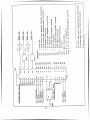
LIST OF FIGURES
1.1
Generic Multi-Processor System
5---------------------5
2.1
Slave-Only Subsystem
0-------------------------------
2.2
Master-Only Subsystem
2.3
------------------------------
11
Master-Slave Subsystem
-----------------------------
13
2.4
Daisy Chain Arbitration
----------------------------
15
2.5
Parallel Arbitration
-------------------------------
16
2. 6
Virtual-Memory-Mapping
-----------------------------
20
2.7
Mapping Mechanism
----------------------------------
21
2
Dual-ported Memory
---------------------------------
22
.8
3. 1
System Block Diagram -------
4
Minimal System
.1
-----------------------
-------------------------------------
25
31
A. 1
MC68010 Signal Groups
C.1
Minimal
C.2
Minimal System HALT* and RESET* Generation Circuitry 119
C.3
Minimal System Clock Generation Circuitry ----------
120
C.4
Minimal System Address Decode Circuitry ------------
121
C.5
Minimal System DTACK* and BERR* Generation Circuitry 122
C.6
Minimal System EPROM and SRAM Circuitry
C 7
Minimal System Interrupt Request and li"Lerrupt
Acknowledge Circuitry
------------------------------ 124
C.8
Minimal System Dual-port Receiver/Transmitter Serial
Port Circuitry
------------------------------------125
E.1
Master Circuit Board Functional Block Diagram ------
132
E.2
System Controller Circuit Board Functional Block
Diagram
--------------------------------------------
133
------------------------------
System MC68010 Microprocessor Circuitry
ix
----
70
118
------------ 123
-------------------
134
E.3
MC68010 Microprocessor Circuitry
E.4
H?.'- * and RESET* Generation Circuitry --------------
135
E.5
Clock Generation Circuitry
-------------------------
136
E.6
Local Bus Address Decode Circuitry
E.7
-----------------
137
Memory Management Unit Circuitry
(Page 1 of 2) -----
138
E.8
Memory Management Unit Circuitry
(Page 2 of 2) -----
139
E.9
Dual-port DRAM Controller Circuitry
(Page 1 of 3)
140
E.10 Dual-port DRAM Controller Circuitry
(Page 2 of 3)
141
E.1l Dual-port DRAM Controller Circuitry
(Page 3 of 3)
142
E.12 Dynamic Random Access Memory Circuitry
(Page 1 of 4)
-------------------------------------- 143
E.13 Dynamic Random Access Memory Circuitry
(Page 2 of 4)
-------------------------------------- 144
E.14 Dynamic Random Access Memory Circuitry
(Page 3 of 4)
-------------------------------------- 145
E.15 Dynamic Random Access Memory Circuitry
(Page 4 of 4)
--------------------------------------
E.16 EPROM and SRAM Circuitry
146
--------------------------- 147
E.17 Dual-port Asynchronous Receiver/Transmitter Serial
Port Circuitry
------------------------------------- 148
------------------------
E.18 Interrupt Handler Circuitry
E.19 DTACK* and BERR* Generation Circuitry -------------E.20 VMEbus Controller Circuitry
149
150
------------------------
151
--------------------
152
E.21 VMEbus Address Decode Circuitry
E.22 Master Circuit Board VMEbus Drivers Circuitry
(Page 1 of 3)
-------------------------------------- 153
E.23 Master Circuit Board VMEbus Drivers Circuitry
(Page 2 of 3)
--------------------------------------
154
E.24 Master Circuit Board VMEbus Drivers Circuitry
(Page 3 of 3)
--------------------------------------
155
x
E.25 VMEbus Arbitration Circuitry--------------------------
156
E.26 SYSRESET* Generation Circuitry-----------------------
157
E.27 System Controller VMEbus Drivers Circuitry-----------158
xi
I.
Economic
pressure
INTRODUCTION
constantly
forces
computer
design
and
technology to produce more cost-effective system implementations.
Computers are made more cost-effective by lowering operating cost
through
increased
speed
and
power
and
by
lowering
design,
maintenance and upgrade costs through modular design techniques.
Architectural innovations can accelerate this process.
Hence, new
innovations in system architecture are constantly sought
after.
Architecture is used here to mean the structuring of the modules
which are organized into a computer system [Ref. l:p. 1].
These
modules include processors, memory and input/output (I/O) devices.
A uni-processor system consists of a single processor subsystem
and various supporting modules integrate1 to form a system.
contrast,
a multi-processor system is
In
comprised of two or more
processor subsystems connected into one interrelated functional
system.
In a multi-processor system, the interconnection of the
processor subsystems must be done in such a way as to maintain
control and manage the data flow of the entire system.
This may be
accomplished through multi-ported memory, a serial link or as in
this thesis, by a system bus.
A number of computer architectural
designs that accommodate growing needs are examined in this thesis.
Key architectural features of bus structures, memory-management and
interrupt control are described in this chapter.
1
Bus structures allow for the integration of peripherals, memory
and application-specific boards into one coherent
system.
Bus
structures permit the exchange of data and control signals between
This allows circuit boards to communicate with
circuit boards.
each other and to share rasources. However, a strict adherence to
protocols must be maintained so the integrity of information and
control is preserved.
Memory-management
virtual-memory.
features
include
memory
protection
and
Special memory schemes have been used to protect
a system's integrity, to make more effective use of its physical
memory's address range and to permit multi-ported memory so that
the memory resource can be shared in a multi-processor system.
memory protection
scheme
prevents
users
from
inadvertently
A
or
maliciously tampering with the operating system, its associated
memory-mapped hardware or
other users.
To
accomplish this,
a
portion of the processor's address range can be reserved for the
operating
system, while the
system users.
remaining portion
is
allocated to
The operating system is protected because the user
is not permitted to cross into the operating system's memory.
The
virtual-memory
aspect
of
memory-management
permits
a
greater dynamic range and flexibility for user memory than actually
exists with the system's physical memory.
Virtual-memory allows
each user to run programs as if he or she has full use of the
processor's address range, independent of the memory used by the
operating system or the other users.
The user is unaware of how
the physical memory in the system is allocated.
2
Therefore, memory
resources can be allocated automatically and respond to the dynamic
needs of the operating system and the users.
In a system without
virtual-memory, programs must be executed in a specific memory
space and for large programs, the user must provide complex overlay
schemes to circumvent the fixed user memory allocation.
difficult
for such a system to
concurrently.
support
several
It
is
large programs
In a virtual-memory system, the operating system
breaks up the user's program into segments called pages and moves
these pages as
needed between physical memory and a secondary
storage device such as a hard disk.
Thus, a virtual-memory system
can easily support several large programs concurrently as long as
each program only requires a modest amount of memory at any given
time.
Multi-ported memory,
such
as
dual-ported
memory,
allows
a
common memory resource to be shared between two or more processors
or peripheral devices.
processors
can
Thus, different processes or different
communicate
with each
other via a multi-ported
memory mailbox equipped with an accompanying semaphore to maintain
access control and data integrity.
Also, multi-porting provides a
communication link between tightly coupled systems where there is
a high degree of interaction.
Interrupts
optimize
the
performance
of
a processor.
An
interrupt is a control signal generated asynchronously by a device,
such as a serial port, requesting service from the processor.
The
processor is free to process other tasks between interrupts from
devices requiring service [Ref. 2:pp. 220-223).
3
When it is ready
to service an interrupting device, the processor saves its current
state and then performs the servicing tasks.
When the servicing
tasks are completed, the saved state of the processor is restored
and the operation prior to the interrupt is resumed. Consequently,
the processing power of the processor is
increased because the
overhead from polling peripheral devices for a service request is
eliminated.
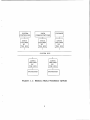
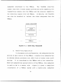
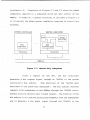
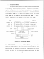
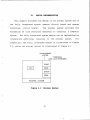
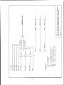
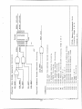
In a general sense, a generic multi-processor system can be
viewed as illustrated in Figure 1.1.
Various subsystems such as
data processing, storage and data communications are
along a system bus to make up a complete system.
comprised
of
memory,
I/O
and
processor
integrated
Each subsystem is
modules
configured
to
accommodate the unique requirements of the users of the multiprocessor system.
entire system.
A system controller acts as the arbiter for the
The system controller directs the information flow,
much as a traffic policeman directs traffic, between the various
subsystems
along
the system bus to ensure
properly coordinated.
that
the
system
is
In order for each subsystem to have access
to the system bus, logic must be incorporated within each subsystem
to allow it to interface to the system bus.
The main thrust of this thesis is to explore the concepts of
bus
structure, memory-management and interrupt control.
These
concepts are addressed in a greater depth than would be possible in
a classroom environment.
4
SYSTEM
CONTROLLER
I
LOGIC
DEFINED
BY
THE BUS
DATA
COMMUNICATIONS
STORAGE
LOGIC
DEFINED
BY
THE BUS
LOGIC
DEFINED
BY
THE BUS
SI
I
I
..............
SYSTEM BUS
LOGIC
DEFINED
BY
THE BUS
LOGIC
DEFINED
BY
THE BUS
PROCESSOR
PROCESSOR
Figure 1.1: Generic Multi-Processor System
5
II.
The
concepts
DESIGN CONCEPTS
addressed in
this
thesis
are
limited to bus
structure organization, memory-management and interrupt control.
These features are commonly used in today's processor systems.
However, many options are available within each area.
design
is
a virtual-memory
implementation
of
This thesis
a MC68010-based
microprocessor system integrated on the VMEbus with dual-ported
memory capability.
Borrill [Ref. 3] highlights several advantages of the VMEbus.
The VMEbus, through its non-multiplexed address
lines and data
lines, does not have multiplexing delays as do other buses, nor
does it have the transactional protocol overheads as do some other
buses.
In addition, the non-multiplexed address lines will support
address pipelining.
For interested readers, Borrill has made a
detailed comparison of the features and performance of the VMEbus,
Futurebus, Multibus II, Nubus and Fastbus (Ref. 3].
In addition to the
VMEbus structure was
advantages that Borrill highlights, the
selected because
of the relative
ease of
integrating Motorola and Signetics peripheral hardware devices.
These hardware devices include a memory management unit, VMEbus
controller, bus arbiter, interrupt handler hardware and dual-port
dynamic random access memory (DRUA_)
The
controller.
following discussion presents
VMEbus structure and memory-management.
6
a broad overview of
the
This should facilitate
understanding of the concepts that are incorporated into the final
system (master circuit board) design.
A.
VMEbus SPECIFICATION
1.
Background
The VMEbus specification originated with Motorola's 68000
microprocessor products.
The 68000 series was introduced to the
marketplace in the late 1970s, using the VERSAbus specification.
In the early
1980s,
Motorola's European Microsystems
group in
Munich, Germany, introduced the Eurocard version of the VERSAbus,
referred to as the VERSAbus-E specification.
A joint agreement was
reached to adopt the VERSAbus-E as the baseline bus specification
for Motorola 68xxx devices with Mostek and Signetics as secondsource suppliers of the 68xxx family of devices.
was
renamed
the
VMEbus.
The
VMEbus
The VERSAbus-E
specification
[Ref.
4]
delineates the mechanical and electrical characteristics of the bus
and the protocols to interface devices on the VMEbus.
2.
VMEbus Description
The
VMEbus
strategies and
offers
support
a versatile
features.
It
combination
of
timing
also offers several
data
transfer sizes, several addressing modes and several arbitration
methods.
The VMEbus is an asynchronous, non-multiplexed bus that
accommodates 8, 16 and 32-bit data transfers. [Ref. 5]
Asynchronous data transfers are flexible and do not impose
timing control signals.
Completion signals from the asynchronous
devices ensure that adequate time is allowed for the data transfer.
In contrast, synchronous data transfers impose a timing constraint
7
on the data transfer which must
accommodate the slowest device
attached to the bus.
A
non-multiplexed
bus
is
one
that
accommodates
data
transfers and address transfers as separate signals on separate
lines of the bus.
This contrasts with the multiplexing strategy
where data signals and address signals share the same set of lines.
As a simple description, during a write cycle, multiplexing address
signals are gated on one clock cycle and data signals are gated on
the
same
lines
during
a
subsequent
clock
cycle.
The
non-
multiplexing strategy speeds up data transfer by eliminating the
second clock cycle.
The
VMEbus
can
be
used
with
24
or
32
address
lines
depending on the microprocessor's requirements and it is easily
adaptable to the entire family of Motorola 68xxx microprocessors
and peripherals.
The VMEbus is composed of four sub-buses that play unique
roles
within
the
overall
VMEbus
functional
structure.
These
include the data transfer bus (DTB), the data transfer arbitration
bus,
the priority interrupt bus and the utility bus.
The VMEbus
functional specification describes how each sub-bus interacts and
the rules which govern the behavior of each sub-bus (Ref. 4:pp. 15194].
The DTB provides the pathways for the data signals, the
address signals and their associated control signals.
of
resolving
bus
ownership
takes
place
on
the
The process
data
transfer
arbitration bus.
The priority interrupt bus is used to accommodate
processes
request
which
servicing
8
from another
subsystem.
An
interrupt
stops
serviced.
The
normal
bus
utilities
activity
bus
"miscellaneous functions bus".
is
until
sometimes
the
interrupt
referred
to
as
is
a
It includes a system reset line, an
alternating current (AC) power failure line, a system failure line
and a system clock [Ref. 2:p. 475].
The design in this thesis uses the VMEbus controller and
the interrupt handler hardware devices which are designed for use
with the VMEbus.
3.
Configurations
In a multi-processor VMEbus-based system with a variety of
peripheral devices, each subsystem can fulfill one of three primary
roles.
The subsystem can serve as a slave-only, as a master-only
or as a master-slave combination.
A subsystem can also have the
role of direct memory access (DMA) in a master-slave configuration.
(To limit the size and complexity of this thesis, the DMA masterslave configuration is not discussed.)
These roles determine the
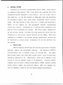
way the subsystem is integrated to the system bus.
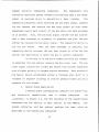
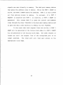
a.
Slave-Only Application
In
the
slave-only
slaved to the VMEbus.
configuration,
the
subsystem
is
In other words, this subsystem is incapable
of making a request to obtain access and control of the VMEbus.
The slave subsystem is a device which other subsystems utilize.
Examples of slave subsystems include communication ports and stand
alone
memory
boards.
If
intelligence
(logic) is
added,
the
subsystem can evolve into an input/output (I/O) channel or a mass
storage
subsystem.
Figure 2.1
shows the simplicity of a slave
9
subsystem
interfaced
to
the
VMEbus.
The
74LS245s
octal-bus
transctivers with 3-state outputs provide the drive capability for
transmitting signals onto the VMEbus and the receiver capability
for receiving signals from the VMEbus.
can
also be disabled to
isolate
If desired, the 74LS245s
the slave
subsystem from the
VMEbus.
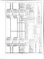
SLAVE SUBSYSTEM
SLAVE
DEVICE(S)
74LS245s
VMEbus
Figure 2.1: Slave-Only Subsystem
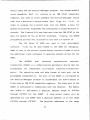
b.
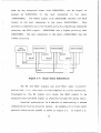
Master-Only Application
In the master-only configuration, the subsystem has the
ability to gain control of the VMEbus.
A master-only subsystem has
an onboard central processor unit (CPU) with or without local slave
devices.
It is interfaced to the VMEbus with a bus controller.
When the subsystem has gained control of the VMEbus, this subsystem
is said to be in a master role.
Figure 2.2 gives a simplified
illustration
with
of
a VMEbus
system
10
a master-only
subsystem
attached to it.
Comparison of Figures 2.1 and 2.2 shows the added
complexity required in a subsystem which can gain control of the
VMEbus.
In addition, a system controller is included in Figure 2.2
to illustrate the added system complexity required to control bus
accesses.
SYSTEM CONTROLLER
MASTER SUBSYSTEM
CPU
--
BUS
ARBITER
LOCALI
DEVICES
BUS
CONTROLLER
74LS244s
74LS245s
VMEbus
Figure 2.2: Master-Only Subsystem
Given
a
request
by
the
CPU,
the
bus
controller
generates a bus request signal through an 74LS245 to the system
controller's bus arbiter.
(The abilities of
described in the slave-only subsystem.)
the 74LS245 were
The bus arbiter receives
requests from subsystems on the VMEbus through the 74LS244 octalbuffers and line drivers with 3-state outputs.
The function of the
bus arbiter is to resolve prioritized requests from the subsystems
and to generate a bus grant
signal through the 74LS244
11
to the
highest
priority
requesting
subsystem.
The
subsystem's
bus
controller maintains system integrity by ensuring that a bus grant
signal
is
received prior
to
permitting a data transfer.
The
requesting subsystem, after receiving the bus grant signal, negates
its bus request
and asserts
the bus busy signal
so that
other
subsystems cannot gain control of the bus while the data exchange
is in process.
Also, the bus busy signal informs the bus arbiter
that a data exchange is currently in progress and that the bus
arbiter can release the bus grant signal.
now the bus master.
When the
data
The requesting device is
exchange
is
complete, the
requesting device releases the bus busy signal to allow the bus
arbiter the opportunity to grant the bus to another subsystem.
If the bus is in use and a higher priority bus request
is asserted, the bus arbiter asserts the bus clear line.
The bus
clear signal informs the current bus master that another subsystem
with a higher priority is requesting bus ownership.
Each potential
bus master should accommodate either a "release when done" or a
"release on request" strategy to resolve pending higher priority
requests for bus access.
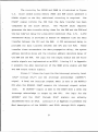
c.
Master-Slave Application
A master-slave configuration combines the master-only
and
slave-only
capabilities
into
a
single
subsystem.
As
illustrated in Figure 2.3, the CPU residing on the master-slave
subsystem has the ability to gain control
system
controller
and
bus
arbiter
perform
described in the master-only subsystem.
12
of the VMEbus.
the
same
roles
The
as
Shared
subsystem.
it
has
slave
devices
are
onboard
the
master-slave
These devices can be accessed by another subsystem when
control
of
isolates
the
74LS244s
outputs
the
shared
VMEbus
slave
into
(Fig. 2.3).
devices
from the
a high impedance
The
bus
CPU
by putting
state,
subsystem accesses the shared slave devices.
controller
the
whenever another
When this happens,
the shared slave devices become a global asset to the system.
The
74LS245s not only act as line drivers and receivers,
SYSTEM CONTROLLER
MASTER-SLAVE SUBSYSTEM
i
BUS
ARBITER
LOCAL
BUS
CONTROLLER
74LS244s
SHARED
SLAVE
DEVICES
74LS244s
74LS245s
VMEbus
Figure 2.3: Master-Slave Subsystem
they also prevent access from the VMEbus to shared slave devices
when
the
appropriate
control
signal
13
is
asserted
by
the
bus
(in this case the CPU) is
Whenever the local master
controller.
accessing the shared slave devices, these devices become a local
As discussed
asset.
master-only
in the
the
application,
bus
controller preserves the VMEbus protocol.
4.
Arbitration Protocols
Arbitration protocols ensure conflict-free access to the
system
bus
from
all
subsystems
processor environment
[Ref.
and are
6:p. 100] .
crucial
in
a
multi-
An arbitration protocol
ensures that only one bus master has access to the bus at a time,
thus safeguarding the bus from collisions in which information is
transferred on the bus by multiple sources.
The VMEbus supports
both serial and parallel arbitration schemes or a combination of
both methods.
These two method are described in the
following
paragraphs.
Daisy
chaining
is
a
method
of
arbitrating
communication bus by serial prioritization.
daisy chain arbitration.
requesting
ownership
must
till
relinquishes control of the bus.
in use,
the
other
controlling
device
any
present
subsystem
bus
master
A subsystem requests access to
the bus by asserting the bus request (BR) signal.
or
shared
Figure 2.4 illustrates
If the bus is
wait
a
acknowledges
the
The bus arbiter
bus
request
by
asserting a bus grant (BG) signal to the bus grant input (BGIN) of
SUBSYSTEMI, the first subsystem in the daisy chain.
If SUBSYSTEM1
is requesting the bus, it asserts the bus busy (BBSY) signal and it
continues
to
negate
its
bus
grant
SUBSYSTEM1 can now begin data transfer.
14
output
(BGOUT)
signal.
If the bus request was
made by any
passed
by
subsystem other than SUBSYSTEM1,
SUBSYSTEM1
(SUBSYSTEM2).
to
the
next
the BG signal
subsystem
in
the
is
chain
The BGOUT signal from SUBSYSTEM1 becomes the BGIN
signal to the next
subsystem in the chain
(SUBSYSTEM2) .
This
process is repeated until the highest priority requesting subsystem
receives the BGIN signal.
SUBSYSTEM2.
SUBSYSTEM1 has a higher priority than
The last subsystem in the chain (SUBSYSTEMn) has the
lowest priority.
BUS
SUBSYSTEMI
ARIE BGOUT
SUBSYSTEM2
BGOUT
BGIN
SUBSYSTEMn
BGOUT
BGIN
BGIN
BBSY
BR
DATA
Figure 2.4: Daisy Chain Arbitration
The BR and BBSY signals
are wire-ORed
(open collector-
active low), i.e., the logic is tied together at a wire connection.
Consequently, the
BR signal
will
cause the
BBSY
signal
to be
asserted once the BGIN signal is received through the daisy chain.
Parallel arbitration is a method of arbitrating a shared
communication bus by priority levels.
An example of a three-level
parallel arbitration scheme is shown in Figure 2.5.
15
In Figure 2.5,
bus request zero
request two
(BRO) has the lowest priority level, while bus
(BR2) has the highest priority level.
The highest
priority subsystem with a pending request is granted access to the
bus.
In this parallel arbitration scheme, the subsystems desiring
use of the bus make bus requests
(BRx) through the bus arbiter.
The bus arbiter or other controlling device then sends out a bus
grant (BGx) onto the bus to the highest priority subsystem with a
pending bus request.
BUS
ARB ITER
SUBSYSTEM2
SUBSYSTEM1
SUBSYSTEM
LBR2U
BG2
BRl
BGl
BRO
BGO
DATA
DATA
Figure 2.5: Parallel Arbitration
The main advantage of the daisy chain arbitration scheme
over the parallel
arbitration scheme is that
inserted sequentially, one after the other.
subsystems can be
Consequently, new
subsystems are easily added to the system.
The main advantage of the parallel arbitration scheme over
the daisy chain
performed faster.
arbitration scheme
is that
arbitration can be
Parallel arbitration does not propagate a bus
grant signal down a chain, but rather the bus grant signal is sent
16
directly to the highest priority
However,
the parallel
arbitration
subsystem requesting service.
scheme
limits the
number
of
subsystems that the bus arbiter can accommodate.
Any
fixed priority
arbitration
cannot
ensure
that the
subsystem with the lowest priority level will be serviced if higher
priority
subsystems
arbitration
and
make
parallel
frequent
requests.
arbitration
methods
The
daisy
may
need
chain
to
be
modified or a controller may need to be incorporated to ensure each
subsystem can be serviced fairly.
The
VMEbus
uses
a serial-parallel
arbitration with only one bus arbiter.
combination
for
bus
VMEbus arbitration uses a
scheme with four parallel priority levels similar to Figure 2.5.
Each priority level, however, can have subsystems daisy-chained as
illustrated in Figure 2.4.
In other words, the bus arbiter grants
bus access 'Co a given level and then the daisy chain at that level
determines which subsystem actually gets the bus.
The VMEbus arbitration process includes the BBSY signal (as
shown in Figure 2.4) and the bus clear (BCLR) signal.
The BBSY and
BCLR lines are added to the bus arbiter and all subsystems on the
VMEbus.
is
The VMEbus BBSY signal is asserted by the subsystem which
granted
bus
access.
The
BCLR
output
signal
informs
all
subsystems on all priority levels that a subsystem on a higher
priority level than the current bus master has requested access to
the VMEbus.
As mentioned earlier, the requesting subsystem should
accommodate a "release when done" or "release on request" strategy
to resolve pending higher priority requests for bus access.
17
B.
MEMORY-MANAGEMENT
Memory-management
can
employ
a combination
of
methods
to
organize the physical memory associated with a microprocessor or
system.
These methods effectively free the programmer using the
system, from being concerned where the program code and program
data will reside in memory.
This thesis addresses the memory-
management concepts of memory protection, virtual-memory and dualported memory.
1.
Memory Protection
One
method
used
to
organize
the
address
range
of
a
microprocessor is to divide its address space into two or more
blocks.
Each block of the address space can be designated for a
specific purpose, such as supervisor memory or user memory.
The MC68010
microprocessor has two modes
of operation.
These modes are the user mode and the supervisor mode.
The user
mode provides an instruction set for the programmer to accommodate
a
majority
of
applications.
The
supervisor
mode
provides
additional instructions and privileges for use by the operating
system and other system-related software [Ref. 7:p. 1-1].
The user memory is the area designated for non-privileged
individuals to use.
user mode.
because
it
Such an individual executes programs in the
The address range for the user is normally limited
does not
include
the addresses
associated with the
operating system and the memory-mapped peripherals.
the
user
is
instructions.
restricted
from
executing
Additionally,
privileged
supervisor
In contrast, the operating system executes programs
18
in supervisor mode and can address supervisory memory and memorymapped peripherals as well as user memory.
This segregation of the
supervisor and the user precludes the user from reconfiguring the
system, but still allows the user access to part of the physical
memory
and to
the
computational
power
of
the
microprocessor.
Typically, the user must request the operating system to perform
operations which the user is not allowed to perform.
2.
Virtual-Memory
Virtual-memory allows programs to be executed which require
more memory space than is physically resident.
Therefore, the
maximum program size is not limited by the size of physical memory.
Originally, this method was designed to reduce and more effectively
use memory.
A virtual address is an address located within the address
space
of
the
microprocessor.
Consequently, with
the
MC68010
microprocessor, there exists 16 megabytes of virtual-memory.
virtual-memory implementation groups the virtual
blocks called pages.
A
addresses into
Figure 2.6 shows such a grouping with zero
through N pages of virtual-memory but with only enough physical
memory to accommodate two virtual pages in physical memory.
In
Figure 2.6, virtual PAGE 1 and virtual PAGE N are mapped into
separate physical pages.
When
address
is
the
CPU generates
translated
into
a virtual
a physical
address,
address.
the virtual
The
address
translation process includes fairly sophisticated memory protection
so that tasks cannot interfere with each other or access resources
19
not allocated to them. Figure 2.7 illustrates a simplified memorymapping
mechanism.
The
high
order
referred to as a virtual page number.
virtual
address
bits
are
The virtual page number
references a location of the translation table.
The translation
table has as its contents a physical page number which references
the starting location of the physical memory's page address.
The
low order virtual address bits give the relative address offset of
the desired address within the physical page selected.
PAGE 0
PAGE 1
PHYSICAL ADDRESS
PAGE N-1
<
PAGE N
VIRTUAL ADDRESS
Figure 2.6: Virtual-Memory-Mapping
Generally, each processing task has its own translation
table similar to Figure 2.7.
the
active
task
changes
These tables are switched whenever
which
processing tasks.
20
avoids
interference
between
VIRTUAL ADDRESS
HIGH ORDER BITS
(VIRTUAL PAGE NUMBER)
LOW ORDER BITS
TRANSLATION TABLE
ADDRESS
WITHIN
PHYSICAL
PAGE 0
PAGE
PAGE N - 1
PAGE
N
PAGE ADDRESS
SELECTED
PHYSICAL ADDRESS
Figure 2.7: Mapping Mechanism
When the CPU generates a virtual address in a page that is
not present in physical memory, for instance PAGE 2 as in Figure
2.7,
the memory manager senses that
fault.
fact and generates a page
The page fault triggers a chain of events which ultimately
retrieves the desired page of the program from secondary storage
and places it in physical memory.
The instruction which caused the
page fault is then continued or restarted. [Ref. 2:pp. 326-330]
21
3.
Dual-ported Memory
Dual-ported memory permits two nearly simultaneous accesses
to the memory resource without conflict.
Figure 2.8 illustrates a
typical configuration of a dual-port memory device.
One approach
to arbitrating concurrent memory requests in a dual-ported random
access memory
(RAM) is to sample one request line on the rising
clock edge and the other on the falling clock edge.
A PORT 1
REQUEST is assumed to be sampled on the rising clock edge.
PORT 1
PORT 2
ADDRESS BUS
-
74LS244s
74LS244s
DATA BUS
-
74LS245s
74LS245s - DATA BUS
CONTROL BUS
-
74LS244s
74LS244s - CONTROL BUS
PORT 1 GRANT
- ADDRESS BUS
PORT 2 GRANT
PORT 1 REQUEST -
DUAL-PORT
M=O:RY DEVICE
PORT 2 REQUEST
CLOCK ADDRESS
BUS
DATA
BUS
MEMORY
Figure 2.8: Dual-ported Memory
If a PORT 1 REQUEST is asserted,
a PORT 1 GRANT is generated which
gates the PORT 1 address, data and control lines through the lefthand 74LS244s and 74LS245s in Figure 2.8.
signals
are
sent
to
the
The address and control
dual-port memory
22
device
and the data
signals are sent directly to memory.
The dual-port memory device
then gates the address lines to memory.
While the PORT 1 GRANT is
active, the PORT 2 GRANT cannot be asserted.
out
from gaining access to memory.
PORT 2 is thus locked
In contrast,
if a PORT 2
REQUEST is asserted and PORT 1 is inactive, a PORT 2 GRANT is
generated.
This causes PORT 2 to gate the control and address
lines through the other 74LS244s to the dual-port memory device and
to gate the data lines directly to memory via the 74LS245s.
In the event that both request lines are active, a PORT 1
GRANT will be generated on the rising clock edge or a PORT 2 GRANT
will be generated on the falling clock edge.
The other request is
locked out until the request line of the recognized port is no
longer asserted.
The other port will
appropriate clock edge.
23
then gain access on the
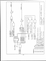
III.
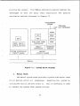
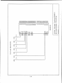
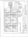
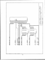
SYSTEM OVERVIEW
This thesis seeks to design a system that satisfies the design
requirements for a system that can be expanded to a multi-processor
system. Additionally, the subsystem design is interrupt-controlled
with both virtual-memory and dual-ported memory support.
This
chapter gives a system perspective on the hardware associated with
the system controller circuit board and master circuit board (Fig.
3.1) integrated to the VMEbus.
A.
SYSTEM CONTROLLER CIRCUIT BOARD
The VMEbus specification describes the system controller as a
board which resides in slot one of the VMEbus back plane (Ref. 4:
pp.
5] .
The
priority bus
interrupt
system
access
controller
circuit
arbitration,
acknowledge
board design
a manual
(IACK*) daisy
provides
system reset
chain driver.
The
and a
system
controller subsystem uses line drivers to buffer the arbitration
signals and IACK* signal on the VMEbus.
1.
Priority Bus Arbitration
The
Motorola
peripheral device
access arbitration.
request
MC68452
[Ref.
8]
bus
was
arbitration
module
(BAM)
selected to perform the VMEbus
The BAM is configured to accommodate four bus
(BRx*) inputs and four bus grant
(BGx*) outputs.
After
parallel arbitration, a bus grant signal is generated by the BAM at
the level of the highest priority bus request.
signal
is then daisy chained down on the
24
The bus grant
level of the highest
priority bus request.
advantages
of
both
This VMEbus arbitration method combines the
the
daisy
chain
arbitration
and
parallel
arbitration methods discussed in Chapter II.
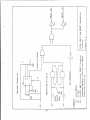
DEVELOPMENT
SYSTEM
TERMINAL
(CRT
and KEYBOARD)
II
DUART
CPU
DRAM
I AMMMU
EPROM
DUAL-PORT DRAM
CONTROLLER
IACK* DAISY
CHAIN DRIVER
VMEbus
CONTROLLER
SYSTEM CONTROLLER
CIRCUIT BOARD
SRAM
INTERRUPT
HANDLER
MASTER
CIRCUIT BOARD
VMEbus
Figure 3.1: System Block Diagram
2.
Manual Reset
The manual system reset provides a system-wide master reset
of all devices within all
subsystems.
initializes various devices within it.
Resetting the
This is necessary in order
to restart the system after system failure.
25
system re-
3.
Interrupt Driver
The VMEbus structure provides the IACK* signal daisy chain.
However, a driver is provided on the system controller circuit
board to drive the IACK* signal onto the VMEbus.
B.
MASTER CIRCUIT BOARD
The master circuit board is the primary design focus of this
thesis.
As shown in Figure 3.1, the master circuit board subsystem
is composed of nine functional blocks.
the
central
processor
unit
(CPU),
These functional blocks are
dual
universal
asynchronous
receiver/transmitter (DUART), dynamic random access memory (DRAM),
static random access memory (SRAM), erasable programmable read-only
memory
(EPROM),
memory
management
unit
(MMU),
dual-port
controller, VMEbus controller and interrupt handler.
DRAM
The master
circuit board is configured in a master-only role as discussed in
Chapter II.
1.
Central Processor Unit
The Motorola MC68010, 16-bit CPU, was selected to be the
processing element because it has the necessary features to support
virtual-memory
architecture.
but
lacks
the
addz
cj::ty
of
a
32-bit
It also affords easier wire-wrap assembly than the
other Motorola CPUs supporting virtual-memory because wire-wrap is
better supported for a dual in-line package (DIP) and there are
fewer data
and
address
signals.
The
signals
and programming
capabilities of the MC68010 microprocessor are discussed in further
detail in Appendix A.
26
2.
Dual Universal Asynchronous Receiver/Transmitter
Two asynchronous serial (RS-232) ports are implemented with
the Motorola MC68681 DUART.
One serial port is configured to drive
a terminal, while the second serial port is used to down-load files
from an IBM XT/AT compatible computer.
The first serial port is
used to permit a human interface to the system.
The intent of the
second serial port is to provide the ability to develop software on
an IBM XT/AT compatible computer with a cross assembler and then to
down-load the software through the second serial port to the master
circuit board's random access memory (RAM) for testing, debugging
and execution.
3.
Erasable Programmable Read-Only Memory
The EPROM in this thesis design, contains the exception
vector
table
and the monitor/debugger program.
The
exception
vector table contains the addresses of the routines to be executed
as a result of
an
interrupt
or
other exception.
The monitor
program configures the subsystem when it is powered up and handles
communications
with
the
terminal
microprocessor and the user.
for
interaction
between
the
It also provides debugging commands
and coordinates the previously mentioned down-loading of files.
Sixty-four kilobytes of EPROM are provided in the master circuit
board.
Once an operating system is developed, it
desirable to
freeze the
interrupt part
table into read-only memory (ROM).
27
would not be
of the exception vector
It should be noted that the
design of an operating system to take advantage of the system's
hardware features is beyond the scope of this thesis.
4.
Random Access Memory
Sixteen kilobytes of SRAM and one megabyte of DRAM are
provided on the master circuit board.
5.
Memory Management Unit
The
use
of
the
Motorola
MC68451
advantages to the microprocessor system.
MMU
affords
several
The MMU provides the
advantages of virtual-memory and a sophisticated memory protection
scheme
(both previously discussed in Chapters
I and II) .
The
MC68451 provides the capability to:
-
Translate logical addresses to physical addresses.
-
Provide segment descriptors to implement memory protection.
-
Detect page faults and other situations requiring operating
system intervention.
-
Aid the operating system in managing the virtual-memory system
efficiently (by use of the segment status registers).
6.
Dual-port DRAM Controller
The Signetics 74F765 dual-port DRAM controller provides
access to the DRAM by either a local bus master or a global bus
master.
If DRAM is accessed by the local bus master, i.e., the CPU
on the master circuit board subsystem, it becomes a local asset.
It is not desirable for the local CPU to access DRAM via the VMEbus
because long access times would be the result.
by a global bus master, i.e.,
another subsystem controlling the
VMEbus, it becomes a global asset.
locally
or
globally
is
If DRAM is accessed
desirable
28
The ability to access DRAM
for
a
system
that
includes
subsystems that interact closely with one another.
the
dual-port
DRAM
controller
provides
refresh
In addition,
cycles
to
the
dynamic memory integrated circuit chips.
The global memory accesses in this master circuit board
subsystem
design,
use
physical
addresses
to
permit
the
implementation of mailboxes with attached semaphores as discussed
in Chapter I.
An operating system needs to lock the mailbox page
in physical memory at a specified physical address.
7.
VMEbus Controller
The
Signetics
VMEbus data transfer
SCB68172
VMEbus
controller preserves the
and VMEbus access protocols.
The VMEbus
controller and the MC68010 CPU are configured in a master-only role
as illustrated in Figure 2.2 and discussed in Chapter II.
The
VMEbus controller provides the necessary logic to interface the
master circuit board subsystem to the VMEbus.
8.
Interrupt Handler
The Signetics SCB68155 interrupt handler is used in the
master
subsystem
processing.
The
design
to
interrupt
assist
handler
the
CPU
receives
with
global
interrupt requests and arbitrates their priority.
interrupt
and
local
The arbitration
priority is non-maskable interrupts, first, then local interrupts
and finally global interrupts.
The interrupt handler acts as a mediator between the CPU
and the interrupting device or between the CPU and the interrupting
subsystem.
Once a local interrupt is generated by the DUART or
MMU, control signals are sent between the interrupting device and
29
the interrupt handler as well as between the interrupt handler and
the CPU.
The DUART or the MMU responds with a pre-programmed
status/ID vector as an interrupt response.
A
subsystem
can
request
an
interrupt
asserting the appropriate interrupt request line.
at
any
time
by
On detecting an
interrupt request, the interrupt handler sends a control signal to
the VMEbus controller to request the VMEbus during the interrupt
acknowledge cycle.
The subsystem making the request then sends the
status/ID vector to the master circuit board's CPU.
30
IV.
DESIGN IMPLEMENTATION
This chapter discusses the design of the minimal system and of
the
fully
controller
integrated
circuit
system
board).
(master circuit
The
minimal
board
system
and
system
provides
the
foundation of core resources necessary to construct a computer
system.
The fully integrated system design can be implemented by
integrating
additional
resources
to
the
minimal
system.
For
comparison, the fully integrated system is illustrated in Figure
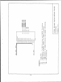
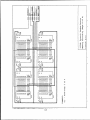
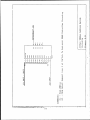
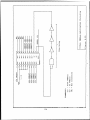
3.1, while the minimal system is illustrated in Figure 4.1.
DEVELOPMENT
SYSTEM
TERMINAL
(CRT and KEYBOARD)
DUART
DRAM
EPROM
SRAM
MINIMAL SYSTEM
Figure 4.1: Minimal System
31
A.
MINIMAL SYSTEM
Currently at the Naval Postgraduate School (NPS), there exists
no computer-aided design (CAD) tools which can simulate the fully
integrated system designed in this thesis.
the inability
This is in part due to
of the CAD vendors to keep pace with the profusion
of extremely complex very large scale integrated (VLSI) circuit
chips.
The CAD systems at NPS, Valid Inc.'s SCALD and Futurenet's
CAD50,
do
not
support
within this thesis.
all
the peripheral
devices
incorporated
Consequently, a step-by-step progression was
made to fully integrate the system.
The first stage, referred to
as the minimal system, includes the core resources which form the
foundation to which more complex devices can be added.
When more
complexity is added to the minimal system, operational testing can
be conducted to insure proper integration of the new devices into
the system.
1.
Memory Map
Memory-mapping determines how the microprocessor accesses
physical
memory and peripheral devices.
The Motorola MC68010
microprocessor has 23 address lines, Al through A23.
The upper
data strobe (UDS*) and lower data strobe (LDS*) lines collectively
determine address bit AO.
Effectively, there are 24 address lines
giving an virtual address range of 16 megabytes.
Physical memory
elements such as static random access memory (SRAM), dynamic random
access memory
(DRAM) and read-only memory
(ROM) are mapped into
this 16 megabyte range as are the memory-mapped peripherals.
32
The memory-mapped peripheral devices have multiple internal
registers.
The high order physical address bits are used to select
a particular peripheral device.
The low order physical address
bits are decoded inside the peripheral device
select
one
of
the
internal
registers.
and subsequently
These
registers
are
programmed to configure the device to meet desired performance
specifications.
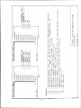
Table I displays the specific locations of the minimal
system's memory-mapped devices and the physical memory components
within the address space of the MC68010 central processor unit
(CPU).
TABLE I: MINIMAL SYSTEM MEMORY MAP
PHYSICAL
ADDRESS
$000000
64K BYTES OF EPROM
$OOFFFF
$010000
16K BYTES OF STATIC RAM
$013FFF
$014000
NOT USED
$7F6FFF
$7F7000
MC68681 DUART
$7F7FFF
$7F8000
NOT USED
$FFFFFF
The
64k bytes of erasable programmable read-only memory
(EPROM) contain the exception vector table and the monitor/debugger
program. Appendix B gives the source code listing of the exception
33
vector table and the monitor/debugger program.
assembler
cross
[Ref.
9),
running on
an
The 2500AD MC68010
IBM XT/AT
compatible
computer, was used to cross assemble the monitor/debugger source
code into a Motorola S-record format (Ref. 10:pp. A-i - A-41.
order to program the S-record code
In
into the EPROM, a Data I/O
System 29 Universal Programmer was configured to accept Motorola Srecords.
The S-record file was then sent from the IBM XT/AT to the
Data I/O System 29 via an RS-232 interface.
Finally, the EPROM
programming process was initiated on the Data I/O System 29.
The
software.
16K
bytes
of
SRAM
are
used
to
test
development
Files can be down-loaded to the SRAM for debugging.
SRAM is used in the minimal system design instead of DRAM to avoid
the additional logic necessary to generate refresh cycles for the
DRAM.
The
MC68681
dual
universal
asynchronous
receiver/
transmitter (DUART) is a communications peripheral device that can
accommodate
ports.
two
independent
full-duplex
(receiver/transmitter)
The operating mode and data format of each port can be
programmed independently.
One port of the DUART is configured by
the monitor/debugger program to accommodate the down-loading of
files from an IBM XT/AT compatible computer.
The other port of the
DUART is configured to communicate with the terminal.
map
(Table I) delineates
through $7F7FFF
a physical
for the DUART.
address
range
A chip select
The memory
of
$7F7000
signal
will be
generated for the DUART when a physical address is in the range
$7F7000
through $7F7FFF.
The physical
34
addresses
in the range
$7F7010 through $7F7FFF are multiple maps for the DUART.
maps provide valid addresses to chip select the DUART.
permit address decoding logic to be simplified.
Multiple
They also
However, to avoid
ambiguity, only the physical addresses $7F7000 through $7F700F are
used to address the DUART.
2.
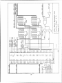
Hardware Interface
Appendix
minimal system.
C
illustrates
the
circuitry
involved
in
the
Figures C.1 through C.8 illustrate the minimum
system in its entirety.
Figure C.1 illustrates the MC68010 microprocessor used in
the minimal system design.
Figure C.2
circuitry.
illustrates
The NE555 timer provides an automatic system reset when
the system is powered up.
switch
the HALT* and RESET* generation
(push button).
There is also a manual system reset
Resetting
the
system
internal circuitry of the CPU and DUART.
the
reset circuitry
unneeded
buffer.
has
one
in
the
the
A two-input OR gate in
input grounded,
However,
initializes
fully
so
it
acts
integrated
as
an
system
(discussed later in this chapter), this input is tied to the VMEbus
system reset (SYSRESET*) line.
This permits a system-wide reset to
the master circuit board illustrated in Figure 3.1.
Figure C.3 illustrates the clock generation circuitry. The
8 MHz CPU
counter
to
oscillator.
clock signal
divide
a 16
is
MHz
produced by using
signal
from
a 74LS161
a crystal
binary
controlled
A 4 MHz signal from the 74LS161 provides the clock
35
input for the shift register which is used to help generate the
data transfer acknowledge (DTACK*) and bus error (BERR*) signals.
Erasable programmable logic devices (EPLDs), specifically
Altera EP310s, were used to reduce the chip count in the minimal
system.
EPLDs were used for address decoding, generating DTACK and
BERR signals, performing interrupt
control
and generating SRAM
write enable and RAM and ROM output enables.
Figure C.4 shows the EPLD implementation for the minimal
system
address
decoder.
The
minimal
implements the memory map of Table I.
system
address
decoder
Listing D.1 in Appendix D
presents the Abel software program for the address decoder.
Abel
software will be discussed in the next section.
Figure C.5 shows the logic of the circuitry which generates
the DTACK* and BERR* signals to the CPU.
The circuitry prior to
the 74LS05 open collector inverters, is implemented by an EPLD.
The DTACK and BERR signals are passed through the 74LS05s to give
the open collector outputs and the proper assertion levels (DTACK*
and BERR*).
In the event that the MC68010 microprocessor tries to
address a location not supported by the design, a bus error (BERR*)
time-out signal is generated after two microseconds.
The BERR*
signal causes the CPU to begin bus error exception processing.
This
invokes the
address $000008.
routine whose address
is
in the
longword
at
The circuit which generates the delay time for
BERR* is referred as a watchdog timer.
Listing D.2 in Appendix D
presents the Abel description of the DTACK and BERR signals.
36
The circuitry for EPROM and SRAM is illustrated in Figure
C.6.
Since random access memory
(RAM) and ROM cannot generate a
DTACK* signal to the CPU, additional circuitry is required.
DTACK* signal
informs the
completed
the
by
slave
CPU that the data transfer has
device.
The
74LS164
shift
The
been
register
generates the data transfer delay times for the RAM and the ROM and
the bus time-out delay for a bus error condition (Fig. C.5) .
A 250
nanosecond delay is provided to ensure an adequate time for data
transfer between the CPU and the RAM.
A 500 nanosecond delay is
provided for data transfer between the CPU and the ROM.
These
transfer times accommodate the data propagation delay, the system
address decoding delay and the internal address decoding delay of
the RAM and the ROM.
The logic for the output enable and the write
enable signals are implemented on an EPLD.
Listing D.3 in Appendix
D presents the Abel description of the SRAM write enable and RAM
and ROM output enable signals.
Figure C.7 shows the logic for the interrupt priority level
(IPLO* through IPL2*)
signal.
and the
interrupt
acknowledge
(IACK681*)
A level one interrupt request (HHL) is sent to the MC68010
CPU when the MC68681 DUART asserts its interrupt request output
(low).
An IACK681* signal is sent to the DUART when a level one
interrupt acknowledge is output by the CPU.
IACK681*
and
the
IPLO*
implemented with an EPLD.
through
IPL2*
The logic for the
signals
are
actually
Listing D.4 in Appendix D presents the
Abel description of the IACK681* and IPLO* through IPL2* signals.
37
Figure C.8 illustrates the circuitry which supports the
dual serial ports.
As mentioned earlier, one port (Port A) of the
DUART is configured to communicate with the terminal.
port
The other
(Port B) is configured by the monitor/debugger program to
accommodate the down-loading of files from an IBM XT/AT compatible
computer.
3.
Software Support
a.
Exception Vector Table and Monitor/Debugger Program
The exception vector table contains the addresses of
routines to be executed when an exception
detected.
The monitor program sets up communications with the
terminal,
provides
command.
The
debugging commands
exception vector table
program
(Appendix B) reside
address
$000000.
addresses
addresses
(trap or interrupt) is
well
as
a down-load
and the monitor/debugger
in the EPROM starting at physical
The exception vector table occupies physical
$000000
through
$000400
monitor/debugger
as
$0003FF
through
program
[Ref.
$001FFF
begins
at
are
the
7:p.
4-5] .
not
used
arbitrarily
Physical
and
the
selected
physical address $002000.
The
monitor/debugger
Motorola Educational
program
Computer Board
(ECB)
was
developed
[Ref.
101.
on
the
After
a
system reset, the microprocessor's program counter is initially
loaded with address $002000 to start the monitor/debugger program.
b.
Monitor/Debugger Commands
The monitor/debugger program provides a user with six
commands.
These commands are not intended to be comprehensive, but
38
they do provide assistance in program development and debugging.
The user commands are as follows:
-
GO address <,break point address>
MM start address <,end address>
MD start address <,end address>
RCH {Axx, Dxx, PC, US, SP, SR}
REG
LOAD
where <...> implies optional
{.. .} implies select one entry
The
GO command is
used to
resides in the system's memory.
execute
a program
that
The program can be placed in
memory by using the memory modify command or by down-loading a
program from an IBM XT/AT compatible computer.
The address in the
GO command gives the location where program execution will begin.
An optional break point address can be added within the GO command.
The
break
specified.
point
will
stop
program
execution
at
the
address
This is particularly useful if one desires to know the
state of the machine, i.e., memory contents or register contents,
at that point.
The memory modify command
(MM) is used to modify the
contents of an address or, if desired, a range of addresses.
This
command can modify code or data residing in RAM.
The memory display command (MD) is used to display the
contents of an address or a range of addresses, if desired.
The change register command (RCH) is used to modify the
contents of an address register (Axx), a data register (Dxx), the
program counter (PC), the user stack pointer (US), the system stack
39
pointer
(SP) or the status register
(SR).
One of these options
must be specified with the RCH command.
The
display
register
command
(REG)
displays
the
contents of the address registers, data registers, program counter,
user stack pointer, system stack pointer and status register.
information gives the
state
of the MC68010.
This
This
command is
particularly useful when a breakpoint is reached in the debugging
process.
The down-load command (LOAD) permits the minimal system
to receive software that was developed on an IBM XT/AT compatible
computer.
After code has been assembled and linked using software
such as the 2500AD MC68010 cross assembler, it can be down-loaded
to the absolute address (or addresses) specified during the linking
process.
c.
Programmable Logic Device Programming
As already mentioned, EPLDs are used to reduce the chip
count on the printed circuit board. The Data I/O Abel
[Ref. 11]
program was used to compile a high-level language representation of
desired digital logic.
The output of Abel is a joint electron
device engineering council
the EPLDs.
(JEDEC) standard file for programming
This file is then down-loaded to the Data I/O System 29
Universal Programmer to program the EPLDs.
Appendix D shows the
Abel source code that generates the logic implementations discussed
in this chapter and illustrated in Figures C.4, C.5, C.6 and C.7.
40
B.
FULLY INTEGRATED SYSTEM
The intent of this thesis is to design a hardware system so
that at some future date an operating system could be developed to
control
its hardware
facilities.
These facilities
accommodate
virtual-memory, protected memory, serial communications, interrupt
control and multi-processor abilities interfaced to the VMEbus.
hard disk controlled by a direct memory access
would be needed to
implement
support virtual-memory.
management
unit
the paging
A
(DMA) controller
function
required to
The operating system would use the memory
(MMU)
to
implement
user/supervisor
allocations (protected memory) and virtual-memory.
memory
Considerations
for a future operating system will be discussed throughout the
following sections.
The fully integrated system is composed of the master circuit
board subsystem and the system controller subsystem
Each subsystem is decomposed into functional units.
(Fig. 3.1).
The functional
units for the master circuit board subsystem are shown in Figure
E.1 and the functional units for the system controller subsystem
are shown in Figure E.2.
Each of the functional units for the
subsystems is discussed in the following sections.
1.
Memory Map
The memory map
physical
address
space
(Table II) of the master circuit board's
contains
devices and the physical memory.
the
memory-mapped
peripheral
This mapping is an
enhanced
version of the minimal system's physical memory map (Table I).
41
TABLE II: SYSTEM MEMORY MAP
PHYSICAL
ADDRESS
$000000
64K BYTES OF EPROM
$OOFFFF
$010000
16K BYTES OF SRAM
$013FFF
$014000
OFF-BOARD RESOURCE
$7F4FFF
$7F5000
MC68451 MMU
$7F5FFF
$7F6000
SCB68155 INTERRUPT HANDLER
$7F6FFF
$7F7000
MC68681 DUART
$7F7FFF
$7F8000
OFF-BOARD RESOURCE
$7FFFFF
$800000
ONE MEGABYTE OF DRAM
$8FFFFF
$900000
OFF-BOARD RESOURCE
$FFFFFF
The memory map allocates
interrupt
vector
table,
64K bytes of ROM to
system.
The
interrupt vector table
perform
the
same
However,
an
roles
operating
handle
the
enormous
memory
allocations
as
the operating
requirements
(protected memory),
system to
reside
42
in
have
memory) and an operating system kernel.
of
and
operating
and monitor/debugger program
described
system would
code
program
monitor/debugger
include the
in
to
the
to
be
minimal
system.
incorporated
to
manage user/supervisor
page
faults
(for virtual-
The intent is for the core
ROM,
since
a mass
storage
A design of
device is not incorporated in this subsystem design.
a multi-disk control module for a VMEbus-based system was presented
in an earlier thesis [Ref. 12].
The 16k bytes of SRAM retains upward compatibility with the
minimal
system.
The SRAM will be used until the DRAM can be
incorporated into the master circuit board subsystem.
However, if
an operating system requires more that the 64K byte size of ROM,
which is a likely possibility, any range spanning the physical
addresses $010000 through $7F4FFF could be allocated for more ROM
or RAM.
This would require changing the address decoding logic and
adding ,%OM or RAM chips to the master
circuit board subsystem
design.
The MC68451 MMU [Ref. 13] is memory-mapped because its
internal registers must be programmed for the desired virtualmemory
configuration
and
address
translation.
By
using
the
MC68010's function codes (see Appendix A) along with the desired
address translation scheme, an operating system can separate the
supervisor's address space
from the user's address space, thus
implementing a memory protection scheme.
The SCB68155 interrupt handler hardware [Ref. 14:pp. 2-369
- 2-3851
is memory-mapped so that it can be initialized for the
desired mode of operation.
The interrupt handler can accommodate
local interrupts from the DUART and the MMU as well as interrupts
from global bus masters.
The MC68681 DUART [Ref. 15] provides the interface to two
RS-232 serial links.
One link is used for communications with the
43
terminal, while the other link is used for communications with an
IBM XT/AT computer.
The DUART is configured to provide the desired
serial communications characteristics such as baud rate, parity and
stop bitE.
One megabyte of DRAM is provided for the master circuit
board subsystem.
The operating system would manage this resource
by assigning virtual pages to physical memory.
a portion
It is intended that
of the DRAM's physical address range map to the same
virtual address range.
This will permit global memory access to
pass semaphores and messages between the master circuit board and
other subsystems, as discussed in Chapter I.
It is important L- note that if an address falls into the
ranges of
$014000
through $7F4FFF,
$7F8000
through
$7FFFFF or
$900000 through $FFFFFF, the CPU is accessing an off-board device.
2.
Master Circuit Board
a.
Microprocessor
The MC68010 CPU (Fig. E.3) is the processing element of
the master circuit board subsystem.
organized into functional groups
The signals of the CPU can be
(see Appendix A) which describe
the role of the signals within the subsystem.
The CPU has two bi-directional open collector pins,
HALT* and RESET*, which require pull-up resistors to ensure that
the signals are not asserted until the appropriate events occur.
The only bus master on the subsystem is the MC68010.
Hence, the bus request (BR*) and the bus grant acknowledge (BGACK*)
44
signals require a pull-up resistor to ensure that the CPU does not
perform bus arbitration.
No Motorola M6800 peripherals are used in the master
circuit board design.
Hence, the valid peripheral address (VPA*)
signal is tied to a logical one.
The circuitry to generate the DTACK* and BERR* signals
(discussed later) are
resistors
are
used
open
to
collector signals.
ensure
that
these
Hence, pull-up
signals
are
not
inappropriately asserted.
b.
Halt and Reset Generation
The
and
HALT*
RESET*
generation
circuitry
(Fig.
E.4) provides manual and automatic power-on subsystem reset to the
CPU and peripheral devices.
The NE555 timer provides an automatic
power-on reset to the subsystem.
The NE555 timer is configured as
a one-shot to generate the power-on reset signal.
This automatic
reset occurs within the first few tenths of a second after the
subsystem is powered on.
the subsystem.
An external system reset can also reset
This system reset is generated from the system
controller subsystem via the VMEbus. A debounced switch is used to
cause a manual reset of the subsystem.
A reset causes the CPU to read into the SP register and
PC register the longword (32-bits) contents of physical addresses
$000000
and $000004,
respectively.
Recall that
ROM begins
at
physical address $000000. Consequently, the two longwords beginning
at physical address $000000 are retrieved from non-volatile memory.
The
initial PC vector at physical address $000004
45
contains the
value $002000, so when this value is read into the PC, execution of
the monitor/debugger program is started.
c.
Clock Generation
The clock generation circuitry
(Fig. E.5)
provides
clocking signals to the CPU and to the peripheral devices.
A
74LS161 binary counter is used to divide the 16 MHz signal from the
crystal oscillator into rates that accommodate the CPU, the MMU,
the dual-port DRAM controller and the interrupt handler hardware.
A 4 MHz signal is sent to additional circuitry to help generate the
DTACK* and BERR* signals.
d.
Local Bus Address Decoding
Once a virtual address is mapped to a physical address,
the local
bus
address
circuitry
decode
(Fig. E.6) is used to
generate chip select signals for RAM, ROM or a peripheral device
based upon the system memory map
EPLDs
[Ref.
16:pp. 2-57
-
2-62]
(Table II).
Two Altera EP310
were used in the design to be
programmed via Abel software [Ref. 11] .
As mentioned earlier, Abel
is software developed by Data I/O Corporation that permits a highlevel language description of the logic function to be programmed
on a EPLD, programmable array logic (PAL) or similar logic device.
e.
Memory Management Unit
The MMU circuitry
(Figs. E.7 and E.8) provides the
subsystem with virtual-memory support and memory protection.
The
address translation from a virtual-address-to-physical-address is
done by this device.
the
operating
Once the MC68451 MMU has been configured by
system,
the
address
46
translation
is
performed
internally within the MMU and is thus hidden from the subsystem
unless a page fault occurs.
The internal details of the MMU are
given in its reference manual [Ref. 13].
A page fault
detects
(FAULT*) signal is generated if the MMU
a write violation
performed successfully.
or
if address translation cannot be
The write violation occurs if an attempt
is made to write to a write-protected portion of physical memory.
If address translation cannot be performed, this denotes to the
operating system that a new memory page may need to be brought into
memory from a hard disk or that there is a system error.
operating
system
configures
the
MMU
to
write-protect
The
memory
segments and to implement virtual-memory-mapping by the MMU.
The circuitry to inhibit virtual-address-to-physicaladdress translation during an interrupt cycle is illustrated in
Figure E.7.
The mapped address strobe (MAS*) and ALL input signals
to the MMU are generated during an interrupt acknowledge cycle.
The physical data strobe generation circuitry
(Fig.
E.8) is used to generate the physical upper data strobe (PUDS*) and
the physical
PLDS*
signals
lower data strobe
are
generated
physical-address translation.
(PLDS*) signals.
during
normal
The PUDS* and
virtual-address-to-
Normal address translation is the
mapping of a virtual address to a physical address without a page
fault occurring.
The physical data strobes will not be generated
if there is a write cycle for a write-protected segment.
accomplished by the write inhibit
MMU.
47
This is
(WIN*) signal generated by the
The
physical
address
strobe
circuitry
(Fig.
E.8)
generates a physical address strobe (PAS*) signal to denote that
the address translation has taken place and the physical address is
valid and stable.
f.
Dual-port DRAM Controller
The dual-port DRAM controller circuitry
(Figs. E.9,
E.10 and E.11) provides two paths into RAM [Ref. 17].
bus master
(the CPU) can be ported to the RAM or a global bus
master can be ported to the RAM via the VMEbus.
are
The local
especially
useful
because
processor
information-carrying semaphores.
Two paths into RAM
subsystems
can
pass
Also, The 74F764 dual-port DRAM
controller provides DRAM refresh.
The
3-state
capability
of
the
74LS244s
(Fig. E.9)
octal-buffers and line drivers with 3-state outputs are used to
isolate one port access to the dual-port DRAM controller from the
other port.
The port is selected by the appropriate clock edge and
control signal to the request input (REQl* or REQ2*) of the 74F764
dual-port DRAM controller.
The control signal for REQ1* of the 74F764 (CS764REQl*)
is generated by the
local bus address decoder and the control
signal for REQ2* of the 74F764
VMEbus address decoder.
(CS764REQ2*) is generated by the
If CS764REQI* is active on a rising clock
edge and SEL2* is not asserted, the local master is granted access
to the 74F764.
The dual-port DRAM controller then asserts SEL1* to
enable the 74LS244s and 74LS245s on the local bus side.
48
If CS764REQ2* is active on a falling clock edge and
SELl* is not asserted, the global bus master is granted access into
the 74F764.
The dual-port DRAM controller then asserts SEL2* to
In each
enable the 74LS244s and 74LS245s for the global bus side.
case, the select line is released after the request signal is no
longer asserted.
If both request lines are asserted and neither select
line is asserted, on the next (rising or falling) clock edge, the
select signal will be generated for the appropriate port access.
The request that is locked out cannot gain access to the dual-port
DRAM controller until the other port has completed its task and is
no longer asserting its request signal.
The
74LS245s
octal-bus
transceivers
with
3-state
outputs, illuistrated in Figure E.10, are used to buffer the data
signals.
Data can be sent between the CPU and the VMEbus, between
the CPU and the DRAM or between the DRAM and the VMEbus.
enable signal
the VMEbus.
The data
(DATAEN*) enables data to flow between the CPU and
The select port one
(SELl*) signal enables data to
flow between the CPU and the DRAM, while the SEL2* signal enables
data to
flow between the
DRAM and the VMEbus.
The data
direction to the 74LS245s is controlled by the read/write
flow
(R/W*)
signal during local DRAM accesses, while the global R/W* signal
(GR/W*) controls the direction for global DRAM accesses.
direction enable
The data
(DDEN) signal controls the data direction flow
between the CPU and the VMEbus.
49
The 74F764 can only effectively accommodate 18 address
lines.
Consequently, additional logic illustrated in Figure E.11
must be incorporated to handle address bit A19, which is required
to give access to the desired one megabyte of RAM.
When
the
row address
strobe
(RAS*) signal
from the 74F764
inactive, the data transfer acknowledge output
(DTACK764) is asserted.
becomes
The DTACK signal of the 74F764 signals
that data has been transferred to or from memory.
g.
Dynamic Random Access Memory
The dynamic random access memory
circuitry
(Figs.
E.12, E.13, E.14 and E.15) provides one megabyte of DRAM for the
mabter circuit board subsystem.
byte blocks.
The DRAM is divided into two 512k
The odd bytes are stored in one 512k byte block
(Figs. E.12 and E.13), while the even bytes are stored in the other
512k byte block (Figs. E.14 and E.15).
The DRAM receives refresh cycles
DRAM controller.
from the dual-port
Although the 74F764 dual-port DRAM controller
seizes control of the DRAM during refresh cycles, a bus arbitration
process is not needed. An 8 MHz clock pulse (RCP) is divided by 64
to produce a refresh request internal to the 74F764.
signal
(REQI* or REQ2*)
is
If no request
asserted on the 74F764,
counter internal to the 74F764 is incremented.
a nine-bit
The counter value
which represents the row in memory to be refreshed is then placed
on output lines MAO through MA8 of the 74F764.
The RAS* signal is
then asserted for four clock cycles to refresh a row in memory.
50
Finally, the RAS*
signal is released and the refresh cycle is
complete.
h.
EPROM and SRAM
The EPROM and SRAM circuitry (Fig. E.16) provide 64k
bytes
of ROM and
16k bytes
of
SRAM.
The EPROM contains
the
resident exception vector table and the monitor/debugger program.
The
SRAM
is
upward
compatible
from
the
minimum
system.
If
additional memory is required by a resident operating system, a
modification to the local bus address decoding logic would permit
the size of ROM or RAM to be increased.
i.
Dual Serial Port
The
MC68681
dual
universal
transmitter serial port circuitry
asynchronous
receiver/
(Fig. E.17) is used to provide
serial communications with the terminal and the IBM XT/AT computer.
Port A is dedicated to the terminal and Port B is dedicated to the
IBM XT/AT ccmputer.
The 3.6864 MHz crystal is used to generate the
baud rates for data transmission for both ports.
provides an interface to the system for the user.
The terminal
The IBM XT/AT is
used to down-load files into the master circuit board subsystem's
memory.
j.
Interrupt Handler
The interrupt handler circuitry (Fig. E.18) provides
the necessary logic to accomnodate interrupts from devices residing
on the master circuit board subsystem and global devices residing
on other subsystems.
The SCB68155 interrupt handler can
51
accommodate six local interrupts, seven global interrupts and a
non-maskable interrupt (NMI).
Local interrupts
(LRQl* through LRQ6*) have a higher
precedence than the global interrupts
(IRQl* through IRQ7*).
The
local interrupt signal LRQ6* has the highest priority, while local
interrupt
signal
LRQI*
has
interrupt
signal
IRQ7*
has
the
lowest
priority.
the highest priority,
interrupt signal IRQ1* has the lowest priority.
The
global
while global
The NMI signal has
priority over local and global interrupts and it is provided for a
catastrophic occurrence such as an alternating current (AC) power
failure.
Local interrupts are generated by the DUART and the
MMU.
The DUART is programmed to provide an interrupt request when
a port buffer full condition is met.
The buffer full condition of
the MC68681 DUART occurs whenever a character is received from the
terminal
keyboard or from the
IBM XT/AT.
The
local
interrupt
generated by the MC68451 MMU occurs when the interrupt bit of the
page status register is set during normal address translation.
When a local or global interrupt occurs, the interrupt
handler hardware generates an interrupt priority level output on
lines
IPLO*
through
IPL2*
to
the
CPU.
The
CPU
responds
by
acknowledging the interrupt with the interrupt acknowledge signal
(IACK*) and places the interrupt level on address lines Al through
A3.
The interrupt handler hardware reads the interrupt
address
lines Al
acknowledged.
through A3 to determine which
If the
interrupt
52
was
level
from a local
level on
is being
device,
the
interrupting device provides the vector number on the local data
bus.
the
If the interrupt was from another subsystem on the VMEbus,
interrupt
acknowledge
VMEbus.
bus
handler
hardware
(BIACK*) signal
to
generates
the VMEbus
a
bus
controller
interrupt
and the
The VMEbus controller obtains control of the data transfer
(DTB) so that an interrupt vector can be obtained from the
interrupting subsystem. The BIACK* signal is only generated if the
bus interrupt level is not masked (within the interrupt handler)
and a local interrupt is not pending.
Once the
local
CPU has
acknowledged the
(local or
global) interrupt request and has obtained an interrupt vector, the
local CPU saves the state of the machine and transfers control to
the appropriate interrupt handling routine.
to perform an interrupt handling routine.
This prepares the CPU
After completion of the
interrupt handling routine, the stored state of the machine is
restored and the CPU resumes processing where it left off at the
interrupt.
k.
[Ref. 7:pp. 4-3 - 4-16; Ref. 18:pp. 5-1 - 5-15]
Data Transfer Acknowledge aiid Bus Error Generation
The data transfer acknowledge and bus error generation
circuitry (Fig. E.19) provides control signals to the CPU.
circuitry physically
resides within a Altera EP310 EPLD.
This
The
DTACK* signal denotes that a data transfer has been completed by
the
slave device
addressed.
The
MC68681
DUART,
AC68451
MMU,
SCB68172 VMEbus controller, SCB68155 interrupt handler and 74F764
dual-port DRAM controller peripheral devices possess the necessary
53
logic to generate their own DTACK* signal to acknowledge receipt or
availability of data.
The master circuit board's RAM and ROM chips cannot
generate their own DTACK* signals so external circuitry must do it
for them.
The DTACK* generation circuitry for the SRAM and ROM
must allow adequate time for the data transfer.
All these DTACK*
signals are ORed together to produce the MC68010 DTACK* input.
If the CPU on the master circuit board makes an offboard access using the off-board (OFFBOARD*) signal to the VMEbus
controller, the DTACK* signal
VMEbus controller.
signal
(DTACKl72*) is generated from the
The off-board device provides a global DTACK*
(GDTACK*) to the VMEbus controller
VMEbus DTACK* line.
(Fig. E.20)
via the
In turn, the VMEbus controller would provide
the DTACK172* signal for the DTACK* circuitry.
This arrangement
permits long access times on the VMEbus.
If the master circuit board's DRAM is being accessed as
a global asset, the GDTACK* signal is generated by the SEL2* and
DTACK764 signals as illustrated in Figure E.11.
The
conditions.
BERR*
signal
is
generated
under
one
of
three
First, the BERR* signal is generated when the maximum
allowable SRAM and ROM data transfer time has been reached and a
DTACK* signal has not been received by the CPU.
Secondly, a global
bus error (BERRl72*) signal can be received from a VMEbus watchdog
timer if the master circuit board subsystem has control of the
VMEbus.
Finally, if a page fault signal (FAULT*) is generated by
the MMU, this also causes a bus error condition.
54
The bus error condition causes exception processing to
occur.
The current state of the machine is saved.
Information
from the saved state of the machine can be used to determine the
cause of the bus error.
This is handled by the bus error exception
routine as part of an operating system.
If the first port of the dual-port DRAM controller is
not active and a refresh cycle is not taking place, a global bus
master can have access to the DRAM.
The master circuit board's CPU
is unaware of the access to the DRAM through the second port.
Consequently, the burden is placed upon a global master or a VMEbus
watchdog timer to provide a global BERR* signal
(GBERR*) on the
VMEbus BERR* line, when appropriate, to the VMEbus controller.
The
GBERR* signal is sent to the BERR* circuitry (Fig. E.19) via the
BERRI72* signal.
1.
VMEbus Controller
The VMEbus controller circuitry
(Fig. E.20) provides
the necessary logic for the master circuit board subsystem to gain
access to the VMEbus.
contr'! signals
The SCB68172 VMEbus controller provides
(VMEEN*, DATAEN* and DDEN) to the master circuit
board subsystem's drivers and transceivers.
VMEbus enable
(VMEEN*) signal is to enable the bus drivers only
when there is an off-board (OFFBOARD*) access.
data
flow
The purpose of the
(DATAEN*) and
its
direction
In addition, the
(DDEN) are
controlled.
Parallel jacks are provided which permit jumper selection of the
master circuit board subsystem's priority on the VMEbus.
55
m.
VMEbus Address Decoding
The VMEbus address decode circuitry (Fig. E.21) permits
access of a global bus master to the second port of the dual-port
DRAM controller and ultimately into DRAM.
gained
control
designated
passing.
of
the
VMEbus,
has
Any subsystem, which has
the
ability
to
access
the
(by the operating system) area of DRAM for semaphore
The
VMEbus
address
decoder provides
the
chip select
signal CS764REQ2* to the dual-port DRAM controller (Fig. E.9) .
If
the CS764REQ2* is asserted when clock edge falls and SELl* signal
of the 74F764 is not asserted, the isolation drivers are enabled to
permit the flow of data and addresses from the global resource to
the DRAM.
n.
VMEbus Drivers
The
drivers
circuitry for the master
(Figs. E.22,
circuit board's VMEbus
E.23 and E.24) provides control of signals
from the local bus to the VMEbus and from the VMEbus to the local
bus.
The VMEbus controller controls the direction of the signal
flow as requested by the CPU.
Whenever the local bus master, the
CPU, is not in control of the VMEbus, all signals from the local
bus are isolated at the drivers by the VMEbus controller.
Thus, in
this case, no signals are gated onto the VMEbus from the local bus.
However, another subsystem, if in control of the VMEbus, has direct
access
to the
global
addresses on
megabyte
of
memory map
DRAM through the
user
the VMEbus
DRAM
in
the
dual-port DRAM controller.
fall
master
(Table II).
56
into
the
circuit
The
range
of
board
subsystem's
the one
3.
System Controller Circuit Board
a.
Bus Arbiter
The VMEbus arbitration circuitry
(Fig. E.25) provides
the logic to arbitrate prioritized bus requests in parallel.
Each
bus request is then daisy chained down to the requesting device.
Each subsystem capable of VMEbus access must have the ability to
provide a bus request at one of four priority levels.
priority signal used is DBG7*, while the
signal used is DBG4*.
(BAM) [Ref.
lowest priority level
The process of resolving the VMEbus requests
was described in Chapter II.
module
The highest
8]
Since the MC68452 bus arbitration
is an asynchronous device, the bus grant
signals (DBGx*) are not guaranteed to be spike-free.
Consequently,
a 50 nanosecond delay circuit is used to disable the DBGx* signals
during the parallel arbitration process.
b.
System Reset
The
system
reset
system-wide master reset.
circuitry
(Fig. E.26)
provides
a
This signal is sent on the VMEbus to all
circuit boards and it is used to reset the entire system much like
the local reset discussed earlier in this chapter.
c.
VMEbus Drivers
The circuitry for the system controller drivers
(Fig.
E.27) provides the drive capability for signals to/from the VMEbus.
Since circuitry was not designed to detect an AC power failure, the
ACFAIL* signal is never asserted.
This signal is input to the non-
maskable interrupt of the interrupt handler
clear
(BCLR*) signal
(Fig. E.17) .
The bus
informs the current bus master that there is
57
a higher pending bus request.
Burden is placed upon the current
bus master to either relinquish control of the bus or to continue
control until its task is completed.
the master circuit
board subsystem
For the sake of simplicity,
was
control upon the completion of its task.
designed to relinquish
Finally, an IACK* daisy
chain driver is provided for VMEbus interrupts.
58
V.
RESULTS
Once the minimal system and fully integrated system hardware
was designed, the schematic drawings drafted and the pin-out list
implemented, software support was required to implement the minimal
system.
The monitor/debugger program required a thorough check of
all its software features.
These software features include the
capability to set and remove a breakpoint, to display and modify
memory, to display and change registers, to start program execution
and to down-load software from a development system.
It was discovered while debugging the down-load portion of the
monitor/debugger program that the 2500AD 68010 cross assembler's
linking process
incorrectly resolved external
references.
The
lirking process generates a file in the Motorola S-record format.
The problem was isolated only after comparing the Motorola S-record
to
Motorola's instruction
2500AD
cross
references.
assembler
format.
was
It
was
improperly
identified that the
resolving
external
A corrected version of the 2500AD cross assembler was
obtained from the vendor that
resolved this problem.
With the
monitor/debugger software developed, the minimal system design was
complete.
The monitor/debugger and vector table were programmed in the
erasable programmable read-only memory (EPROM) with the Data I/O
System 29 Universal Programmer.
The Data I/O System 29 segregated
59
the even bytes and odd bytes into separate EPROMs as required by
the Motorola MC68010 central processor unit (CPU).
Erasable programmable logic devices (EPLDs) were used to reduce
the chip count in the minimal system design.
The minimal system
used an EPLD to perform the interrupt request
interrupt acknowledge (IACK681*) logic.
(IRQ681*) and the
Also, EPLDs were used to
implement the circuit logic required for the generation of the data
transfer acknowledge (DTACK) and the bus error (BERR) signals and
for address decoding.
In order to program the EPLDs, Abel software
was used to compile the source code representation of the logic to
be implemented with the EPLD.
Once all of the source code for the
EPLDs had been written, compiled and software tested, the EPLDs
were programmed.
On the Data I/O System 29, once the EPLD is programmed, the
test vectors are again tested against the programmed EPLD.
this
test
run,
the
System 29
failed
for
every EPLD
programmed, even though they passed the software tests.
During
that
was
On the
advice of an applications engineer at Data I/O Corporation, the
test vectors were removed from the source code.
compiled, then the EPLDs were programmed.
boarded,
while
determining
with
This code was
The EPLDs were bread-
reasonable
certainty
that
the
devices were actually implementing the desired logic.
The ultimate goal in this thesis was to implement the master
circuit board subsystem design.
goal
requires the
One of the steps to achieve this
memory management
virtual address to a physical address.
60
unit
(MMU) to
translate a
To avoid significant wiring
modifications to the minimal
system to build up to the master
subsystem, the MMU was wire-wrapped into the minimal system 'iesign.
However, the MMU was not programmed at the minimal system stage.
The MMU translates a virtual address to the same physical address
when the MMU is not programmed after being reset.
The MMU was
configured to accommodate an automatic, manual and programmed (CPU
reset instruction) reset.
61
VI.
A.
SUMMARY AND CONCLUSIONS
SUMMARY
The
goal
of this
thesis was
two-fold:
first,
to
explore
hardware ramifications of designing a microprocessor system for a
multi-processor
environment;
and
secondly,
to
implement
the
minimal system design.
1.
Design Concepts
In exploring hardware ramifications, the scope was limited
to
features
of
the VMEbus
interrupt control.
structure,
in memory-management
and
The memory-management features included memory
protection, dual-ported memory and virtual-memory.
a.
VMEbus Structure
The VMEbus permits an exchange of data and control
beyond the boundaries of a single circuit board.
Other subsystems
or circuit boards which may include processing elements, memory
and/or input/output (I/O) devices can be integrated to the VMEbus.
A strict
adherence to data transfer protocols
over the VMEbus
ensures the reliability and integrity of the system.
The ability
to integrate various subsystems along the VMEbus supports a multiprocessor environment.
b.
Memory-Management
The
Motorola
MC68010
central
processor
unit
(CPU)
generates function codes which can be used by the memory management
unit (MMU) to partition memory into supervisor and user portions.
62
An operating system would manage memory partitioning.
Normally,
systems are designed so that the supervisor memory portion contains
the memory-mapped I/O devices and the read-only memory (ROM) and
some
random
access
memory
(RAM).
The
ROM
is
mapped
to
the
supervisor portion of memory since it provides the exception vector
table and start-up program.
The
operation,
function codes
the supervisor
reflect
and user.
the
The
CPU's two modes
supervisor mode
of
is a
privileged mode which permits access to all instructions and the
full range of memory (supervisor and user memory).
permits access
to
only user instructions
The user mode
and the user memory.
Typically, in the user mode, permission must be granted through the
operating
system
to
use
system resources.
The
separation of
supervisor memory from user memory prevents the user from tampering
with the system assets or gaining supervisor privileges.
Dual-ported memory
permits two
separate
sources
to
access the same memory block and provides the refresh signals for
the
dynamic
random
access
memory
(DRAM) .
permits RAM to be used as a shared asset.
when
a portion
of
the
physical
RAM
is
Dual-ported memory
It is especially useful
dedicated
to
passing
parameters between microprocessor subsystems. Dedicating a portion
of RAM for parameters is analogous to a mailbox delivery system.
The mail courier (subsystem 1) delivers mail
mailbox
(RAM).
(parameters) and
occupant
The addressee
responds
(subsystem 2)
as
(parameters) to the
(subsystem 2) picks up the mail
required.
places mail
63
If
appropriate,
the
(parameters) in the mailbox
(RAM) to be delivered (to subsystem 1).
These parameters can be
used in managing a multi-processor operating system.
A MC68010-based system typically has memory-mapped I/O
devices, RAM and ROM.
DRAM is added the master circuit board
subsystem to supplement the minimal system's static random access
memory (SRAM).
megabytes.
The MC68010 CPU has a virtual address range of 16
However,
the
physical
RAM's
size
considerably less than the size of the virtual
is
usually
address space.
Virtual-memory is used to extend the range of programming beyond
the range of physical RAM.
An MMU is used to map virtual addresses
into RAM physical addresses.
Also, the MMU detects an attempt by
the CPU to access a virtual-memory address which is not currently
present in physical memory.
When such an attempt is detected, the
MMU generates a page fault.
This page fault causes the page fault
exception routine to be invoked.
The exception routine reads a
page of information from secondary storage into RAM.
The MMU maps
the virtual addresses associated with the page into addresses in
the
physical RAM.
After completion of the
exception routine,
program execution resumes with the completion of the instruction
that caused the page fault.
c.
Interrupt Control
Using interrupts results in more effective use of the
microprocessor because the microprocessor is not kept waiting for
a device to respond.
The devices requesting interrupts in this
thesis are programmed to provide an interrupt vector number during
an interrupt acknowledge cycle for local interrupts.
64
The interrupt
vector number causes the address of the exception routine to be
obtained from the exception vector table by the CPU so that it can
be executed.
2.
Design Implementation
a.
Hardware Configurations
The recommended wiring configurations that accompanied
the product specifications for the MMU, VMEbus controller, dual
universal asynchronous receiver/transmitter (DUART), dual-port DRAM
controller, interrupt handler hardware and bus arbitration module
(BAM) greatly assisted in the designs of the minimal system, system
controller subsystem and master circuit board subsystem.
However,
in order to integrate these components into a system, care was
taken to ensure that the control signals were interfaced properly.
Since no computer-aided design
(CAD) tools existed at the Naval
Postgraduate School (NPS) to fully simulate even the minimal system
design, prototyping the minimal system was necessary.
system has a foundation of core resources.
The minimal
The intent was to prove
the system design by building up a master circuit board subsystem
from the minimal system.
The system controller subsystem provides a bus arbiter,
interrupt acknowledge
reset.
(IACK*) daisy chain driver and system-wide
The bus arbiter determines bus ownership between subsystems
that make bus requests and it grants bus ownership to the subsystem
with the highest priority.
An IACK* daisy chain driver sends the
IACK* signal on to the bus during an interrupt acknowledge cycle.
65
The system reset is used to reset all devices on all subsystems
after a system failure.
The master circuit board subsystem accommodates the
VMEbus structure, virtual-memory-mapping facilities, a protected
memory scheme, dual-ported memory and interrupt handling hardware.
The master circuit board subsystem design is an extension of the
minimal system and should not be implemented until the minimal
system is operational.
In the master circuit board subsystem, the
VMEbus controller provides the necessary logic to meet the VMEbus
Drivers
specification foi setting up the baseline bus structure.
and transceivers
are incorporated to meet the
specified signal
drive capability and isolation requirements.
b.
Erasable Programmable Logic Devices
The erasable programmable logic device (EPLD) used in
the minimal system's address decoding must be modified to include
the additional memory-mapped devices cf the master circuit board
subsystem.
The EPLD used for interrupt handling in the minimal
system is replace by the interrupt handler hardware in the master
circuit board subsystem design.
The
master
circuit
board
upgraded version of the minimal system.
wiring connections
was
developed
subsystem
design
an
A pin-out list for all
in order to reduce wire-wrap
errors, but it is not included as part of this thesis.
scale integrated circuit
is
The small
(SSI) logic shown for the generation of
the data transfer acknowledge (DTACK), bus error (BERR), physical
upper data strobe (PUDS*), physical lower data strobe (PLDS*) and
66
physical address strobe
(PAS*) signals was actually implemented
with EPLDs to reduce the chip count.
B.
CONCLUSIONS
Meeting all the goals set in this thesis made this thesis an
ambitious undertaking.
The major integrated circuit
(IC) chips
included the CPU, DUART, interrupt handler hardware, dual-port DRAM
controller,
required
MMU,
an
VMEbus
extensive
application notes
programming
invoked
controller
and
study
product
of
investigation.
These
IC
chips
specification
and
to understand the wiring configurations and
of the devices.
support
BAM.
ideas
in
Study of the specification notes
the
design
that
required
further
These support ideas included DRAM memory refresh
accommodations,
driver
virtual-memory.
Once each device was reasonably understood, the
characteristics,
noise
reduction
and
problem of integrating the devices into a single system remained.
Care was exercised to ensure that control signals were properly
integrated to the devices.
Consequently, a major portion of this
thesis was spent in the research and design process without the
assistance of CAD tools.
The
design
and
almost two years.
implementation work
of
this thesis
spanned
A major problem encountered was the inability to
simulate the system designs.
Hence, the system's validity could
only be verified by actual design implementation.
The design phase took a considerable length of time because the
inter-relationships
between
the
devices
processor environment, dual-port memory,
67
to
support
a
multi-
virtual-memory, memory
protection, dual serial ports and interrupt control features were
not trivial.
Some of these features should have been eliminated so
that a simpler design could have been implemented. However, using
the approach of building a complex subsystem from a minimal system
is an important technique.
For a growing number of new application
IC chips, facilities to simulate designs using these chips do not
yet exist.
Thus, there is a strong need for advanced design tools
and engineering practices to support complex designs.
An important restriction of the master circuit board subsystem
design is the lack of an operating system.
The capability provided
in this thesis could not be fully utilized without an operating
system and a mass storage device, such as a hard disk.
Managing
the virtual-memory and protected memory requirements would require
a tremendous amount of code which is beyond the scope of this
thesis.
However,
while
designing
the
master
circuit
board
subsystem, foresight was exercised to consider the requirements of
an
operating system.
between
system
This
designers
confirms the
and
operating
communicate the system requirements.
68
need
system
for
a dialogue
designers
to
APPENDIX A: MC68010 16-BIT MICROPROCESSOR
Since the entire hardware system design
revolves about the
MC68010 microprocessor, a description of the microprocessor, its
external signals and its programming is appropriate.
A.
MC68010 DESCRIPTION
The MC68010 has seventeen 32-bit general purpose registers, a
16
megabyte
address
space,
virtual-memory/machine
support,
57
instructions with 14 addressing modes using five main data types
and memory-mapped input/output
(I/O)
[Ref. 7:p. 1-1]
Motorola
provides a complete signal description and timing analysis of the
MC68010 microprocessor [Ref. 18].
B.
MC68010 SIGNALS
The MC68010 central processing unit
package.
(CPU) comes in a 64-pin
As shown in Figure A.1, the signals are organized into
groups and the direction of the
signal flow
is denoted by the
arrows.
To avoid any confusion over logic assertion levels, the
asterisk
( * ) at the end of a signal name is used to denote an
active low assertion level.
1.
Address Bus
The address bus
consists of 23 address
eight megaword address range for the CPU.
69
lines giving an
Vcc(2) ->
MISCELLANEOUS
=>
ADDRESS BUS A1-A23
<=> DATA BUS DO-D15
GND(2) ->
->
CLK
FCO
PROCESSOR
STATUS
<>
FC
_FC2
<
E
<-
VMA*
VPA*
->
>
>
<M6800
PERIPHERAL
CONTROL
ASYNCHRONOUS
UDS*
LDS*
BUS
CONTROL
DTACK*-
MC68010
<-
BR*
> BG*
<BGACK *
<-
BERR* ->
RESET* <->
-CHALT* <->
SYSTEM
CONTROL
-
> AS*
R/W*
BUS
ARBITRATION
CONTROL
<IPLO*
<IPL1*
<-- IPL2*
INTERRUPT
CONTROL
Figure A.l: MC68010 Signal Groups
2.
Data Bus
The
data
bus
is
a
16-bit
bi-directional
bus
used
for
transferring byte or word length data.
3.
Asynchronous Bus Control
The
asynchronous bus
control
group provides
about the data that is being transferred.
information
The address strobe (AS*)
signal signifies that valid address signals are being gated from
the
CPU.
The
read/write
reading from a device
the device
(R/W*) line
denotes
that
the
CPU
is
(active high) or that the CPU is writing to
(active low).
The upper data strobe
(UDS*) indicates
that the data being transferred is on an even byte boundary.
The
lower data strobe (LDS*) indicates that the data being transferred
is on an odd byte boundary.
When UDS* and LDS* are both asserted,
a word (16-bits) of data is being transferred.
70
The UDS* and LDS*
signals together determine address bit AO, thus giving an address
range of 16 megabytes for the CPU.
control
the flow of the data
Table III [Ref. 18:p. 4-2] .
The UDS*, LDS* and R/W* signals
on the data bus as
illustrated in
Finally, the data transfer acknowledge
(DTACK*) signal informs the CPU that the current data transfer has
been
completed
by
the
peripheral
device
or
memory
location
addressed.
TABLE III: DATA STROBE CONTROL OF THE DATA BUS
UDS* LDS* R/W*
1
0
1
0
1
0
0
1
lor0
1
1
1
0
0
1
0
0
1
D8 - D15
DO - D7
NO VALID DATA BITS
VALID DATA BITS
NO VALID DATA BITS
VALID DATA BITS
NO VALID DATA BITS
VALID DATA BITS
VALID DATA BITS
NO VALID DATA BITS
0
VALID DATA BITS
VALID DATA BITS
0
0
#VALID DATA BITS 0-7 VALID DATA BITS
VALID DATA BITS
#VALID DATA BITS 8-15
# These conditions are a result of current implementation and
may not appear on future devices.
4.
Bus Arbitration Control
As a group, the bus arbitration control signals provide a
mechanism
these
master
for the CPU to give up control
signals
gets
do
not
control.
determine
The bus
of the bus.
(directly) which
request
However,
alternate
(BR*) signal
is
a signal
generated by a device or devices requesting access to the bus.
bus grant
(BG*) is a signal
bus
The
from the CPU indicating that it will
release the bus at the end of the current bus cycle.
71
The bus
grant acknowledge (BGACK*) is a signal asserted by an alternate bus
master while it has control of the bus.
5.
Interrupt Control
The interrupt priority levels
(IPLO* through IPL2*)
are
signals which represent the encoded priority level for the highest
priority device desiring interrupt service.
The signal IPLO* is
the
IPL2*
least
significant
bit
and
significant bit of the group.
the
signal
is
the
most
A level zero interrupt (all signals
are asserted high) indicates there is no interrupt request pending.
A level seven interrupt
(all IPLx* signals are asserted low) has
the highest priority and is non-maskable.
This implies that level
seven is not an ordinary interrupt level for requesting routine
interrupt
service.
Rather,
a level
seven
interrupt should be
reserved for catastrophic events such as alternating current
(AC)
power failure where the non-maskable property is essential.
6.
System Control
The system control group is used to reset the CPU and to
indicate to the CPU that a bus error has occurred.
It is also used
to reset peripheral devices and to generate a bus error exception.
The halt signal
(HALT*), active low, is a bi-directional signal.
As an input, it is used to stop the CPU at the completion of the
current bus cycle.
As an output, HALT* is asserted only when a
double bus error or address error exception has caused the MC68010
to enter a halt state.
The
directional
reset
signal.
signal
(RESET*),
active
It can be used as
72
an
low,
is
also
input to
a bi-
reset the
internal microcircuitry within the CPU.
When a reset instruction
is executed by the CPU, it can be used to reset system devices.
Typically, a maximum time is allotted for data transfer.
If the data transfer is not completed within the allotted time, bus
error (BERR*) is asserted by a time out circuit called a watchdog
timer.
Often, the BERR* signal is used to inform the CPU that the
current address on the address bus is invalid because no physical
memory or peripheral device is mapped at that address.
signal
can also be used to
making an
attempt
to
write
The BERR*
flag the condition that the CPU is
to
read-only memory
(ROM).
In a
virtual-memory system, BERR* is asserted by the memory management
unit (MMU) when a page fault occurs.
7.
M6800 Peripheral Control
The M6800 peripheral control group is a group of signals
which are used to interface the MC68010's 16-bit asynchronous data
bus to synchronous peripheral devices in the Motorola M6800 eightbit family.
The enable
(E) signal which acts as the 6800 phase two
clock is used to synchronize data transfer between the MC68010 CPU
and M6800 peripheral device.
The E signal's period is ten clock
periods of the MC68010's clock input.
The valid peripheral address
(VPA*) signal denotes to the CPU that the device selected is a
M6800 peripheral device.
The VPA* signal indicates to the CPU that
it should initiate a data transfer synchronized with the E signal.
The valid memory address (VMA*) signal from the CPU indicates to a
73
M6800 device that there is a valid address on the address bus and
that the MC68010 is synchronized with the E signal.
Processor Status
8.
The MC68010 has three function code lines (FCO through FC2)
which delineate the current processor state
and the address space
(program or data) being accessed as defined
by Table IV [Ref. 18:p. 5-3].
the
CPU
indicates
(user or supervisor)
that
a
The address strobe (AS*) signal from
valid
address
and
function
code
are
available from the CPU.
TABLE IV: STATE AND ADDRESS SPACE
ADDRESS SPACE
FUNCTION CODE OUTPUT
FC2
FCl
FCO
0
0
0
0
0
1
UNDEFINED, RESERVED FOR FUTURE USE
USER DATA SPACE
0
0
1
3.
1
1
1
1
0
0
1
1
0
1
0
1
0
1
USER PROGRAM SPACE
UNDEFINED, RESERVED FOR FUTURE USE
UNDEFINED, RESERVED FOR FUTURE USE
SUPERVISOR DATA SPACE
SUPERVISOR PROGRAM SPACE
CPU SPACE (INTERRUPT ACKNOWLEDGE)
9.
Miscellaneous
Both Vcc pins and both GND pins must be connected in order
to power the CPU.
The clock (CLK) input signal is used to develop
all the synchronizing signals required within the CPU.
74
C.
PROGRAMMING
Motorola provides
manual
[Ref.
71.
programming
The
MC68010's
information
in
instruction
set
its
reference
includes
the
following operations:
-
Data Movement
Integer Arithmetic
Logical
Shift and Rotate
Bit Manipulation
-
Bit Manipulation
Binary Coded Decimal (BCD) Arithmetic
Program Control
System Control
Multi-processor Communications
supporting the following data types:
- Bit
-
BCD
Byte
Word
Long
Fourteen
(Four-bits)
(Eight-bits)
(16-bits)
Word (32-bits)
addressing
language programmer.
modes
that
are
available
to
assembly
The addressing modes available include:
- Data Register Direct
- Address Register Direct
- Address Register Indirect
- Address Register Indirect with Postincrement
- Address Register Indirect with Predecrement
- Address Register Indirect with Offset
- Address Register Indirect with Index and Offset
-
the
Absolute Short
Absolute Long
Program Counter with Offset
Program Counter with Index and Offset
Immediate Data
Quick Immediate
Implied Register
75
The following assets are available:
- Eight Data Registers
- Seven Address Registers
- User Stack Pointer (User Mode)
- Supervisor Stack Pointer (Supervisor Mode)
- Program Counter
- *Status Register
(Supervisor mode)
- Vector Base Register (Supervisor Mode)
- Alternate Function Code Registers (Supervisor Mode)
*
The condition code register is the lower byte of the
status register and it is accessible in the user mode.
To support virtual-memory, the MC68010 microprocessor allows an
interrupted bus cycle to be re-run after a bus error exception.
The return from exception
of the exception stack
(RTE) instruction uses the format field
to determine
caused by bus or address error.
whether the exception was
After a bus or address error
caused the exception, the CPU continues the interrupted instruction
after completion of the exception routine. [Ref. 19]
76
APPENDIX B: MINIMAL SYSTEM EXCEPTION VECTOR TABLE AND
MONITOR/DEBUGGER PROGRAM
This appendix contains the source listings of the exception
vector table and monitor/debugger program.
The separate file names
are as follows:
- VECTABLE.ASM
- MAIN.ASM
-
MESSAGE.ASM
CONSOLE.ASM
GETSTRIN.ASM
GET ADDR.ASM
10 UTIL.ASM
DECODER.ASM
BYTEOUT.ASM
MEM LIST.ASM
HEXCONV.ASM
- GO.ASM
- STUB.ASM
- REG.ASM
- REGCHANG.ASM
- DOWNLOAD.ASM
- UNUSED.ASM
Using the 2500AD 68010 cross assembler and linker, a Motorola
S-record format file was generated as a load module.
module was
loaded as
Universal Programmer.
a ASCII
file
into a Data
I/O
The load
System
29
Once resident in the programmer, the load
module was programmed to erasable programmable read-only memory
(EPROM).
It should be noted that the data section as contained in
MAIN.ASM was not programmed on EPROM, but rather it resides in
random access memory (RAM).
The first two entries in the exception vector table are used
during the system boot up to provide the initial contents for the
stack pointer and the program counter.
The exception vector table
contains the addresses of exception routines.
77
The monitor/debugger
program
initializes the MC68681
peripheral
device and provides
facilities for performing software debugging and the down-loading
of files from an IBM XT/AT compatible computer.
78
EXCEPTION VECTOR TABLE
*
*
WRITTEN BY LARRY ABBJTT JUNE 5,
*
FILENAME: VECTABLE.ASM
* VERSION 1.3
* REV
DATE
*
A
29 SEPT 87
*
*
*
*
*
*
*
1987
ORG 0
LONG
LONG
LONG
LONG
LONG
LONG
LONG
LONG
LONG
LONG
LONG
LONG
ORG $38
LONG
LONG
ORG $60
LONG
LONG
LONG
LONG
LONG
LONG
LONG
LONG
*
*
*
NAME
DAVID M.
SENDEK
DESCRIPTION
ADDITIONAL DOCUMENTATION
DEFINING MODULES OF EXTERNALLY DECLARED VARIABLES:
BKPT
- GO.ASM
INIT
- MAIN.ASM
INIT SP
- MAIN.ASM
MESSAGE
- MESSAGE.ASM
MONITOR
- MAIN.ASM
UNUSED
- UNUSED.ASM
EXTERNAL
EXTERNAL
*
*
*
*
*
*
*
*
*
*
BKPT, INIT, INITSP,MESSAGE,MONITOR
UNUSED
VECTOR TABLE STARTS AT ABSOLUTE ADDRESS $000000
INIT SP
INITIAL STACK POINTER VECTOR
INIT
INITIAL PROGRAM COUNTER (PC)
VECTOR
UNUSED
BUS ERROR VECTOR
UNUSED
ADDRESS ERROR VECTOR
UNUSED
ILLEGAL INSTRUCTION VECTOR
UNUSED
ZERO DIVIDE VECTOR
UNUSED
CHK INSTRUCTION VECTOR
UNUSED
TRAPV INSTRUCTION VECTOR
UNUSED
PRIVILEGE VIOLATION VECTOR
UNUSED
TRACE VECTOR
UNUSED
LINE 1010 EMULATION VECTOR
UNUSED
LINE 1111 EMULATION VECTOR
NOTE: VECTOR NUMBERS 12 AND 13
ARE UNASSIGNED,RESERVED
UNUSED
FORMAT ERROR VECTOR
UNUSED
UNINITIALIZED INTERRUPT VECTOR
NOTE: VECTOR NUMBERS 16-23 ARE
UNASSIGNED,RESERVED
UNUSED
SPURIOUS INTERRUPT VECTOR
UNUSED
LEVEL 1 AUTOVECTOR VECTOR
UNUSED
LEVEL 2 AUTOVECTOR VECTOR
UNUSED
LEVEL 3 AUTOVECTOR VECTOR
UNUSED
LEVEL 4 AUTOVECTOR VECTOR
UNUSED
LEVEL 5 AUTOVECTOR VECTOR
UNUSED
LEVEL 6 AUTOVECTOR VECTOR
UNUSED
LEVEL 7 AUTOVECTOR VECTOR
79
LONG
BKPT
LONG
LONG
LONG
LONG
LONG
LONG
LONG
ORG $100
UNUSED
UNUSED
UNUSED
UNUSED
UNUSED
UNUSED
UNUSED
LONG
MONITOR
LONG
LONG
LONG
LONG
LONG
LONG
LONG
LONG
LONG
LONG
LONG
LONG
LONG
LONG
LONG
LONG
LONG
LONG
LONG
LONG
LONG
LONG
LONG
LONG
LONG
LONG
LONG
LONG
LONG
LONG
LONG
LONG
LONG
LONG
LONG
LONG
LONG
LONG
LONG
UNUSED
UNUSED
UNUSED
UNUSED
UNUSED
UNUSED
UNUSED
UNUSED
UNUSED
UNUSED
UNUSED
UNUSED
UNUSED
UNUSED
UNUSED
UNUSED
UNUSED
UNUSED
UNUSED
UNUSED
UNUSED
UNUSED
UNUSED
UNUSED
UNUSED
UNUSED
UNUSED
UNUSED
UNUSED
UNUSED
UNUSED
UNUSED
UNUSED
UNUSED
UNUSED
UNUSED
UNUSED
UNUSED
UNUSED
TRAP 0 VECTOR USED AS
MONITOR BRKPT
TRAP 1 VECTOR
TRAP 2 VECTOR
TRAP 3 VECTOR
TRAP 4 VECTOR
TRAP 5 VECTOR
TRAP 6 VECTOR
TRAP 7 VECTOR
NOTE: VECTOR NUMBERS 48-63 ARE
UNASSIGNED,RESERVED
USER INTERRUPT 0
VECTOR
DEFINED FOR MONITOR
USER INTERRUPT 1
VECTOR
USER INTERRUPT 2
VECTOR
USER INTERRUPT 3
VECTOR
USER INTERRUPT 4
VECTOR
USER INTERRUPT 5
VECTOR
USER INTERRUPT 6
VECTOR
USER INTERRUPT 7
VECTOR
USER INTERRUPT 8
VECTOR
USER INTERRUPT 9
VECTOR
USER INTERRUPT 10
VECTOR
USER INTERRUPT 11
VECTOR
USER INTERRUPT 12
VECTOR
USER INTERRUPT 13
VECTOR
USER INTERRUPT 14
VECTOR
USER INTERRUPT 15
VECTOR
USER INTERRUPT 16
VECTOR
USER INTERRUPT 17
VECTOR
USER INTERRUPT 18
VECTOR
USER INTERRUPT 19
VECTOR
USER INTERRUPT 20
VECTOR
USER INTERRUPT 21
VECTOR
USER INTERRUPT 22
VECTOR
USER INTERRUPT 23
VECTOR
USER INTERRUPT 24
VECTOR
USER INTERRUPT 25
VECTOR
USER INTERRUPT 26
VECTOR
USER INTERRUPT 27
VECTOR
USER INTERRUPT 28
VECTOR
USER INTERRUPT 29
VECTOR
USER INTERRUPT 30
VECTOR
USER INTERRUPT 31
VECTOR
USER INTERRUPT 32
VECTOR
USER INTERRUPT 33
VECTOR
USER INTERRUPT 34
VECTOR
USER INTERRUPT 35
VECTOR
USER INTERRUPT 36
VECTOR
USER INTERRUPT 37
VECTOR
USER INTERRUPT 38
VECTOR
USER INTERRUPT 39
VECTOR
80
LONG
LONG
LONG
LONG
LONG
LONG
LONG
LONG
LONG
LONG
LONG
LONG
LONG
LONG
LONG
LONG
LONG
LONG
LONG
LONG
LONG
LONG
LONG
LONG
LONG
LONG
LONG
LONG
LONG
LONG
LONG
LONG
LONG
LONG
LONG
LONG
LONG
LONG
LONG
LONG
LONG
LONG
LONG
LONG
LONG
LONG
LONG
LONG
LONG
LONG
LONG
LONG
UNUSED
UNUSED
UNUSED
UNUSED
UNUSED
UNUSED
UNUSED
UNUSED
UNUSED
UNUSED
UNUSED
UNUSED
UNUSED
UNUSED
UNUSED
UNUSED
UNUSED
UNUSED
UNUSED
UNUSED
UNUSED
UNUSED
UNUSED
UNUSED
UNUSED
UNUSED
UNUSED
UNUSED
UNUSED
UNUSED
UNUSED
UNUSED
UNUSED
UNUSED
UNUSED
UNUSED
UNUSED
UNUSED
UNUSED
UNUSED
UNUSED
UNUSED
UNUSED
UNUSED
UNUSED
UNUSED
UNUSED
UNUSED
UNUSED
UNUSED
UNUSED
UNUSED
USER
USER
USER
USER
USER
USER
USER
USER
USER
USER
USER
USER
USER
USER
USER
USER
USER
USER
USER
USER
USER
USER
USER
USER
USER
USER
USER
USER
USER
USER
USER
USER
USER
USER
USER
USER
USER
USER
USER
USER
USER
USER
USER
USER
USER
USER
USER
USER
USER
USER
USER
USER
81
INTERRUPT
INTERRUPT
INTERRUPT
INTERRUPT
INTERRUPT
INTERRUPT
INTERRUPT
INTERRUPT
INTERRUPT
INTERRUPT
INTERRUPT
INTERRUPT
INTERRUPT
INTERRUPT
INTERRUPT
INTERRUPT
INTERRUPT
INTERRUPT
INTERRUPT
INTERRUPT
INTERRUPT
INTERRUPT
INTERRUPT
INTERRUPT
INTERRUPT
INTERRUPT
INTERRUPT
INTERRUPT
INTERRUPT
INTERRUPT
INTERRUPT
INTERRUPT
INTERRUPT
INTERRUPT
INTERRUPT
INTERRUPT
INTERRUPT
INTERRUPT
INTERRUPT
INTERRUPT
INTERRUPT
INTERRUPT
INTERRUPT
INTERRUPT
INTERRUPT
INTERRUPT
INTERRUPT
INTERRUPT
INTERRUPT
INTERRUPT
INTERRUPT
INTERRUPT
40
41
42
43
44
45
46
47
48
49
50
51
52
53
54
55
56
57
58
59
60
61
62
63
64
65
66
67
68
69
70
71
72
73
74
75
76
77
78
79
80
81
82
83
84
85
86
87
88
89
90
91
VECTOR
VECTOR
VECTOR
VECTOR
VECTOR
VECTOR
VECTOR
VECTOR
VECTOR
VECTOR
VECTOR
VECTOR
VECTOR
VECTOR
VECTOR
VECTOR
VECTOR
VECTOR
VECTOR
VECTOR
VECTOR
VECTOR
VECTOR
VECTOR
VECTOR
VECTOR
VECTOR
VECTOR
VECTOR
VECTOR
VECTOR
VECTOR
VECTOR
VECTOR
VECTOR
VECTOR
VECTOR
VECTOR
VECTOR
VECTOR
VECTOR
VECTOR
VECTOR
VECTOR
VECTOR
VECTOR
VECTOR
VECTOR
VECTOR
VECTOR
VECTOR
VECTOR
LONG
UNUSED
USER INTERRUPT 92
VECTOR
LONG
LONG
LONG
LONG
LONG
LONG
LONG
LONG
LONG
LONG
LONG
LONG
LuNG
LONG
LONG
LONG
LONG
LONG
LONG
LONG
LONG
LONG
LONG
LONG
LONG
LONG
LONG
LONG
LONG
LONG
LONG
LONG
LONG
LONG
LONG
LONG
LONG
LONG
LONG
LONG
LONG
LONG
LONG
LONG
LONG
LONG
LONG
LONG
LONG
LONG
LONG
UNUSED
UNUSED
UNUSED
UNUSED
UNUSED
UNUSED
UNUSED
UNUSED
UNUSED
UNUSED
UNUSED
UNUSED
UNUSED
UNUSED
UNUSED
UNUSED
UNUSED
UNUSED
UNUSED
UNUSED
UNUSED
UNUSED
UNUSED
UNUSED
UNUSED
UNUSED
UNUSED
UNUSED
UNUSED
UNUSED
UNUSED
UNUSED
UNUSED
UNUSED
UNUSED
UNUSED
UNUSED
UNUSED
UNUSED
UNUSED
UNUSED
UNUSED
UNUSED
UNUSED
UNUSED
UNUSED
UNUSED
UNUSED
UNUSED
UNUSED
UNUSED
USER
USER
USER
USER
USER
USER
USER
USER
USER
USER
USER
USER
USER
USER
USER
USER
USER
USER
USER
USER
USER
USER
USER
USER
USER
USER
USER
USER
USER
USER
USER
USER
USER
USER
USER
USER
USER
USER
USER
USER
USER
USER
USER
USER
USER
USER
USER
USER
USER
USER
USER
VECTOR
VECTOR
VECTOR
VECTOR
VECTOR
VECTOR
VECTOR
VECTOR
VECTOR
VECTOR
VECTOR
VECTOR
VECTOR
VECTOR
VECTOR
VECTOR
VECTOR
VECTOR
VECTOR
VECTOR
VECTOR
VECTOR
VECTOR
VECTOR
VECTOR
VECTOR
VECTOR
VECTOR
VECTOR
VECTOR
VECTOR
VECTOR
VECTOR
VECTOR
VECTOR
VECTOR
VECTOR
VECTOR
VECTOR
VECTOR
VECTOR
VECTOR
VECTOR
VECTOR
VECTOR
VECTOR
VECTOR
VECTOR
VECTOR
VECTOR
VECTOR
82
INTERRUPT
INTERRUPT
INTERRUPT
INTERRUPT
INTERRUPT
INTERRUPT
INTERRUPT
INTERRUPT
INTERRUPT
INTERRUPT
INTERRUPT
INTERRUPT
INTERRUPT
INTERRUPT
INTERRUPT
INTERRUPT
INTERRUPT
INTERRUPT
INTERRUPT
INTERRUPT
INTERRUPT
INTERRUPT
INTERRUPT
INTERRUPT
INTERRUPT
INTERRUPT
INTERRUPT
INTERRUPT
INTERRUPT
INTERRUPT
INTERRUPT
INTERRUPT
INTERRUPT
INTERRUPT
INTERRUPT
INTERRUPT
INTERRUPT
INTERRUPT
INTERRUPT
INTERRUPT
INTERRUPT
INTERRUPT
INTERRUPT
INTERRUPT
INTERRUPT
INTERRUPT
INTERRUPT
INTERRUPT
INTERRUPT
INTERRUPT
INTERRUPT
93
94
95
96
97
98
99
100
101
102
103
104
105
106
107
108
109
110
111
112
113
114
115
116
117
118
119
120
121
122
123
124
125
126
127
128
129
130
131
132
133
134
135
136
137
138
139
140
141
142
143
LONG
LONG
LONG
LONG
LONG
LONG
LONG
LONG
LONG
LONG
LONG
LONG
LONG
LONG
LONG
LONG
LONG
LONG
LONG
LONG
LONG
LONG
LONG
LONG
LONG
LONG
LONG
LONG
LONG
LONG
LONG
LONG
LONG
LONG
LONG
LONG
LONG
LONG
LONG
LONG
LONG
LONG
LONG
LONG
LONG
LONG
LONG
LONG
END
UNUSED
UNUSED
UNUSED
UNUSED
UNUSED
UNUSED
UNUSED
UNUSED
UNUSED
UNUSED
UNUSED
UNUS;ED
UNUSED
UNUSED
UNUSED
UNUSED
UNUSED
UNUSED
UNUSED
UNUSED
UNUSED
UNUSED
UNUSED
UNUSED
UNUSED
UNUSED
UNUSED
UNUSED
UNUSED
UNUSED
UNUSED
UNUSED
UNUSED
UNUSED
UNUSED
UNUSED
UNUSED
UNUSED
UNUSED
UNUSED
UNUSED
UNUSED
UNUSED
UNUSED
UNUSED
UNUSED
UNUSED
UNUSED
USER
USER
USER
USER
USER
USER
USER
USER
USER
USER
USER
USER
USER
USER
USER
USER
USER
USER
USER
USER
USER
USER
USER
USER
USER
USER
USER
USER
USER
USER
USER
USER
USER
USER
USER
USER
USER
USER
USER
USER
USER
USER
USER
USER
USER
USER
USER
UbER
83
INTERRUPT
INTERRUPT
INTERRUPT
INTERRUPT
INTERRUPT
INTERRUPT
INTERRUPT
INTERRUPT
INTERRUPT
INTER.2UPT
INTERRUPT
INTERRUPT
INTERRUPT
INTERRUPT
INTERRUPT
INTERRUPT
INTERRUPT
INTERRUPT
INTERRUPT
INTERRUPT
INTERRUPT
INTERRUPT
INTERRUPT
INTERRUPT
INTERRUPT
INTERRUPT
INTERRUPT
INTERRUPT
INTERRUPT
INTERRUPT
INTERRUPT
INTERRUPT
INTERRUPT
INTERRUPT
INTERRUPT
INTERRUPT
INTERRUPT
INTERRUPT
INTERRUPT
INTERRUPT
INTERRUPT
INTERRUPT
INTERRUPT
INTERRUPT
INTERRUPT
INTERRUPT
INTERRUPT
INTERRUPT
144
145
146
147
148
149
150
151
152
153
154
155
156
157
158
159
160
161
162
163
164
165
166
167
168
169
170
171
172
173
174
175
176
177
178
179
180
181
182
183
184
185
186
187
188
189
190
191
VECTOR
VECTOR
VECTOR
VECTOR
VECTOR
VECTOR
VECTOR
VECTOR
VECTOR
VECTOR
VECTOR
VECTOR
VECTOR
VECTOR
VECTOR
VECTOR
VECTOR
VECTOR
VECTOR
VECTOR
VECTOR
VECTOR
VECTOR
VECTOR
VECTOR
VECTOR
VECTOR
VECTOR
VECTOR
VECTOR
VECTOR
VECTOR
VECTOR
VECTOR
VECTOR
VECTOR
VECTOR
VECTOR
VECTOR
VECTOR
VECTOR
VECTOR
VECTOR
VECTOR
VECTOR
VECTOR
VECTOR
VECTOR
*
*
*
*
MAIN IS THE ENTRY POINT INTO THE MONITOR. MAIN
INITIALIZES THE RS-232 PORT BEFORE ENTERING THE
MONITOR. ALSO, MAIN CONTAINS THE MEMORY MAPS,
EQUATES AND MEMORY ALLOCATIONS.
*
*
*
*
*
*
*
68K MONITOR VERSION V1.3 - AN ACCUMULATION OF ALL
PRIOR VERSIONS
COPYRIGHT @ AUG. 1986 BY DR. LARRY ABBOTT
*
*
*
*
FILENAME: MAIN.ASM
*
* VERSION
*
*
*
*
*
1.3
REV. MODIFIED BY
A
LARRY ABBOTT
B
LARRY ABBOTT
C
LARRY ABBOTT
D
DAVID M. SENDEK 29
*
DATE
DESCRIPTION
11/7/86
12/14/86 MONSTAT-ESCAPE
6/6/87
ADAPT TO MC68681
SEPT 67
-INCLUDE VECTOR TABLE
-INCLUDE MONITOR PROMPT
-CORRECT FOR 68681
*
*
*
*
*
DEFINING MODULES OF EXTERNALLY DECLARED V2'RIABLES:
CMD DECODE
- DECODER.ASM
GETSTRING
- GETSTRIN.ASM
MESSAGE
- MESSAGE.ASM
MONMSG
- MESSAGE.ASM
SCRLF
- 10 UTIL.ASM
*
*
*
*****~*******************************************%************
*
*
*
*
*
*
GLOBAL
rLOBAL
GLOBAL
GLOBAL
GLOBAL
GLOBAL
GLOBAL
GLOBAL
GLOBAL
EXTERNAL
EXTERNAL
DATA
*
.
*
BS
CR
EPROMRNG
ESC
FWDARW
LF
*
*
*
*
*
*
*
BKPTAB, BS,BTLEN,BUFFIN, CHECKSUM, CKSUM
CONTINUE,CR
END ADDRESS,EPROMRNG, EPROMWR, ESC,ESCAPE
FOUND,FWDARW, HEX ERR, LF,MODIFY,MONSTAT,
NULL, PORT1, PORT2,RBA, RECFULL
SPACE, SRA, SRAM, SRAMSIZE, STRING, STRINGEND
SYSTAX, SRB, TBA, TBB, RBB
TBA,XEMPTY
INIT SP,INIT,MONITOR
CMD DECODE,GETSTRING, MESSAGE,MONMSG, SCRLF
PROMPT
ALL R/W DATA IS STORED IN SRAM AT ADDRESS
$010000
EQUATES
EQU
EQU
EQU
EQU
EQU
EQU
$08
$OD
$3FF
$1B
$3E
$OA
ASCII
ASCII
EPROM
ASCII
ASCII
ASCII
CODE FOR
CODE FOR
RNG 0 ->
CODE FOR
CODE FOR
CODE FOR
84
<-- (BACKSPACE)
RET'JRN
$3FF (EXCEPTION TBL)
ESCAPE
'>' (FORWARD ARROW)
LINEFEED
NULL
SPACE
BTLEN
EQU
EQU
EQU
$00
$20
$10
ASCII CODE FOR NUL
ASCII CODE FOR SPACE
BREAKPOINT TABLE LENGTH IN WORDS
MEMORY ALLOCATIONS
*
,
BKPTAB
BUFFIN
END ADDRESS
MONSTAT
STAX
SYSTAX
CK SUM
SRAM
SRAMSIZE
INITSP
BLKW
BLKB
BLKW
BLKW
BLKW
BLKW
BLKW
EQU
EQU
EQU
3/2*BTLEN
$3F
2
1
36
2
1
BKPTAB
$3FFF
$013FFE
RESERVE BTLEN/2 32-BIT BKPT's
RESERVE 63 BYTE INPUT BUFFER
RESERVE WORD FOR END ADDRESS
RESERVE A WORD FOR MONITOR STATUS
SAVE AREA FOR APPLICATION REG'S
RESERVE MEMORY FOR STACK POINTER
CHECK SUM STORAGE
DATA BEGINS AT LOW ADDR OF SRAM
16K BYTES OF STATIC RAM
INITIAL STACK POINTER
DEFINITION OF MONSTAT
EPROMWR
ESCAPE
CONTINUE
FOUND
HEX ERR
MODIFY
STRING
SfRINGEND
CHECKSUM
RECFULL
XEMPTY
MR1RFSET
CLK SRC
CONF IAB
CONF 2A
CONF 2B
BAUD2400
BAUD9600
EN PORT
RUPTeiASK
RUPTVECT
WRITE TO EPROM FLAG
ESCAPE FLAG
CONTINUATION FLAG
CMD FOUND FLAG
HEX CONVERSION ERROR
MEMORY MODIFY FLAG
STRING BUILDING IN PROGRESS
END OF STRING BUILDING
CHECKSUM ERROR FLAG
EQU
EQU
EQU
EQU
EQU
EQU
EQU
EQU
EQU
EQU
EQU
EQU
$00
$02
$1A
$30
$13
$07
$OF
$88
$BB
$45
$02
$40
SRA(0)=1=>RECEIVE FIFO HAS A CHAR
SRA(2)=1=>XMIT HOLDING REG EMPTY
RESET MODE REG PTR & DISABLE XMIT/RECV
XTAL/16 CLOCK
8-BIT DATA, NO PARITY
1 STOP BIT
2 STOP BITS
2400 BAUD
9600 BAUD
RESET ERROR, ENABLE XMIT & RECV
ENABLE RECV READY RUPT
USER INTERRUPT 0 VECTOR
68681 REGISTESRS
*
*
0
1
2
3
4
5
6
7
8
68681 EQUATES
*
*
*
*
EQU
EQU
EQU
EQU
EQU
EQU
EQU
EQU
EQU
(MONITOR STATUS WORD)
CRT
<- PORT A:9600 BAUD,8 DATA BITS,
NO PARITY,1 STOP BIT
DOWNLOAD <- PORT B:2400 BAUD,8 DATA BITS,
NO PARITY,2 STOP BITS
85
DUART
PORT1
PORT2
MR1A
MR2A
SRA
CSRA
CRA
RBA
TBA
IPCR
ACR
ISR
IMR
CUR
CTUR
CLR
CTLR
MR1B
MR2B
SRB
CSRB
CRB
RBB
TBB
IVR
OPCR
EQU
EQU
EQU
EQU
EQU
EQU
EQU
EQU
EQU
EQU
EQU
EQU
EQU
EQU
EQU
EQU
EQU
EQU
EQU
EQU
EQU
EQU
EQU
EQU
EQU
EQU
EQU
$7F7000
DUART
DUART+$10
1
1
3
3
5
7
7
9
9
$B
$B
$D
$D
$F
$F
$11
$11
$13
$13
$15
$17
$17
$19
$1B
BASE ADDRESS FOR MC68681
PORT A
PORT B
R/W:MODE REG 1 FOR PORT A
R/W:MODE REG 2 FOR PORT A
R
:STATUS REGISTER FOR PORT A
W:CLOCK SELECT REGISTER A
W:COMMAND REGISTER FOR PORT A
R
:RECEIVER BUFFER FOR PORT A
W:TRANSMITTER BUFFER FOR PORT A
R
:INPUT PORT CHANGE REGISTER
W:AUXILIARY CONTROL REGISTER
R
:INTERRUPT STATUS REG
W:INTERRUPT MASK REGISTER
R
:COUNTER MODE: CURRENT CNTR MSB
W:COUNTER/TIMER UPPER REGISTER
R
:COUNTER MODE: CURRENT CNTR LSB
W:COUNTER/TIMER LOWER REGISTER
R/W:MODE REG 1 FOR PORT B
R/W:MODE REG 2 FOR PORT B
R
:STATUS REGISTER FOR PORT B
W:CLOCK SELECT REGISTER B
W:COMMAND REGISTER FOR PORT B
R
:RECEIVER BUFFER FOR PORT B
W:TRANSMITTER BUFFER FOR PORT B
R/W:INTERRUPT VECTOR REGISTER
W:OUTPUT PORT CONFIGURATION REG
CODE
INIT:
LEA
DUART,A4
CLR.W MONSTAT
MOVE.B #MRIRESET,CRA(A4)
*
MOVE.B #MR1RESET,CRB(A4)
*
MOVE.B #CLK SRC,ACR(A4)
MOVE.B #CONF_IAB,MRIA(A4)
MOVE.B #CONF 2A,MR2A(A4)
MOVE.B #BAUD9600,CSRA(A4)
MOVE.B #CONFIAB,MR1B(A4)
MOVE.B #CONF 2B,MR2B(A4)
MOVE.B #BAUD2400,CSRB(A4)
MOVE.B #RUPTVECT,IVR(A4)
MOVE.B #ENPORTCRA(A4)
MOVE.B #ENPORT,CRB(A4)
MOVE.B #RUPTMASK,IMR(A4)
A4 <-- PTR TO DUART
CLR MONITOR STATUS WORD
RESET PORT A MR1 PTR,
DISABLE XMIT & RECV
RESET PORT B MR1 PTR,
DISABLE XMIT & RECV
CNTR/TMR CLK FROM CRYSTAL/16
PORT A:8 DATA BITS & NO
PARITY
PORT A: 1 STOP BIT
PORT A: 9600 BAUD
PORT B:8 DATA BITS & NO
PARITY
PORT B: 2 STOP BITS
PORT B: 2400 BAUD
SET DUART INTERRUPT SERVICE
AT USER INTERRUPT 0
RESET ERRS & ENABLE
XMIT/RCV
RESET ERRS & ENABLE
XMIT/RCV
RUPT WHEN PORT A RCVS CHAR
86
*
*
BANNER:BSR
LEA
BSR
BSR
LEA
BSR
LOOP: BRA.S
SCRLF
MONMSG,A5
MESSAGE
SCRLF
PROMPT,A5
MESSAGE
LOOP
MONITOR: MOVE.L
MOVEM.L
LEA
MOVEM.L
BSR
BCLR.B
BEQ
BCLR.B
BSR
LEA
BSR
MOVE CURSOR TO NEXT LINE
SET MESSAGE POINTER TO MONMSG
CRT<--68010 MONITOR V1.3
MOVE CURSOR TO NEXT LINE
SET UP FOR A PROMPT TO THE CRT
SEND PROMPT TO CRT
WAIT FOR AN INTERRUPT
SP,SYSTAX
AO-A7/DO-D7,-(SP)
STAX,A6
(A6)+,AO-A5/DO-D7
GETSTRING
#STRINGEND,MONSTAT
RESTORE
#STRING,MONSTAT
CMD DECODE
PROMPT,A5
SAVE PTR TO APPL REGs
SAVE ALL REGISTERS
SET MONITOR STATE PTR
GET LAST MONITOR STATE
ENTER MONITOR
CHECK FOR END OF STRING
NOT THE END, SO EXIT
CLEAR NEW STRING FLAG
IF END THEN DECODE
SET MSG PNTR TO PROMPT
MESSAGE
CRT <-
RESTORE: MOVEM.L AO-A5/DO-D7,-(A6)
MOVEM.L (SP)+,AO-A7/DO-D7
RTE
END
87
'>'
(CRT PROMPT)
SAVE MONITOR STATE
RESTORE ALL REGISTERS
*
THIS PROGRAM OUTPUTS MESSAGES TO THE CRT SCREEN.
*
*
WRITTEN BY DR. LARRY ABBOTT
*
*
FILENAME: MESSAGE.ASM
*
* VERSION
*
*
*
1.3
REV. MODIFIED BY
A
DAVID M. SENDEK
*
*
DATE
DESCRIPTION
*
29 SEPT 87 -INCLUDE A MONITOR PROMPT*
-INCLUDE BUFFER FULL
*
CONDITION
*
DEFINING MODULES OF EXTERNALLY DECLARED VARIABLES:
ECHO1
- CONSOLE.ASM
*
*
GLOBAL
GLOBAL
GLOBAL
EXTERNAL
CR
LF
NULL
EQU
EQU
EQU
MESSAGE:MOVE.B
BKPTMSG, EPROMSG,ERRMSG, HEXMSG, ILLMSG
MONMSG, REGERR, REGMSG, SRECERR,USEMSG
MESSAGE,PROMPT,BUFFULLMSG, SPCE
ECHO1
$OD
$OA
$00
(A5)+,DO
*
MSGRET:
BEQ.S
BSR
BRA.S
RTS
BKPTMSG: BYTE
BYTE
ERRMSG:
BYTE
BYTE
EPROMSG: BYTE
BYTE
HEXMSG:
BYTE
BYTE
ILLMSG:
BYTE
BYTE
MONMSG:
BYTE
BYTE
BYTE
BYTE
REGERR:
BYTE
BYTE
MSGRET
ECHO1
MESSAGE
ASCII CODE FOR RETURN
ASCII CODE FOR LINEFEED
ASCII CODE FOR NUL
;GET MESSAGE CHAR,
INCREMENT POINTER
IF CHAR = NULL THEN EXIT
;OUTPUT CHAR TO CONSOLE
;GET ANOTHER CHARACTER
'BREAKPOINT TRAP AT '
NULL
'ERROR RE-ENTER',CR,LF
NULL
'ATTEMPTED WRITE TO EPROM',CR,LF
NULL
'HEX CONVERSION ERROR.. .RE-ENTER',CR,LF
NULL
'ILLEGAL INSTRUCTION TRAP',CR,LF
NULL
'68010 MONITOR V1.3',CR,LF
'WRITTEN BY DR. LARRY ABBOTT',CR,LF
'@ COPYRIGHT 1986',CR,LF
NULL
'REGISTER CONTENTS ERROR RE-ENTER',CR,LF
NULL
88
*
*
REGMSG:
BYTE
BYTE
BYTE
BYTE
BYTE
BYTE
BYTE
SRECERR: BYTE
BYTE
USEMSG:
BYTE
BYTE
BYTE
BYTE
PROMPT:
BYTE
BYTE
SPCE:
BYTE
BUFFULLMSG: BYTE
BYTE
END
'D0'I,NULL,' Dl=',NULL,' D2=',NULL,' D3=',
NULL, CR, LF
'D4=',NULL,' D5=',NULL,' D6=',NULL,' D7=',
NULL, CR, LF
'AO=',NULL,' Al=',NULL,' A2=',NULL,' A3=',
NULL, CR, LF
'A4=',NULL,' A5=',NULL,' A6=',NULL,' A7=1,
CR, LF
'SR=',NULL,' PC=',NULL,'
(PC)=',NULL,CR,LF
'US=',NULL,' SS=',NULL,CR,LF
NULL
'S RECORD ERROR MESSAGE',LF,CR
NULL
'UNUSED EXCEPTION ENCOUNTERED',LF,CR
'WITH FORMAT WORD
NULL
f
NULL
I
NULL
LF,CR,'INPUT BUFFER IS FULL, TRY AGAIN.',LF,CR
NULL
89
*
THIS MODULE INPUTS FROM THE KEYBOARD AND DOWNLOAD PORT,
*
*
AND IT OUTPUTS CHARACTERS TO THE CRT.
*
*
NEW CONSOLE WRITTEN DEC. 19, 1986
*
*
FILENAME: CONSOLE.ASM
*
************************************************
*
*
*************
VERSION 1.3
REV. MODIFIED BY
*
*
A
B
BY DR. LARRY ABBOTT
DATE
DESCPIPTION
LARRY ABBOTT
6/6/87
ADAPT TO 68681
DAVID M. SENDEK 30 SEPT 87 DOCUMENTATION UPGRADE
*
DEFINING MODULES OF EXTERNALLY DECLARED VARIABLES:
*
*
*
*
*
*
*
*
ESCAPE
MONSTAT
PORT1
PORT2
RECFULL
RBA,RBB
SRA,SRB
TBA,TBB
-
MAIN.ASM
MAIN.ASM
MAIN.ASM
MAIN.ASM
MAIN.ASM
MAIN.ASM
MAIN.ASM
MAIN.ASM
GLOBAL
GLOBAL
GLOBAL
EXTERNAL
EXTERNAL
EXTERNAL
ESC
EQU
ECHOI,ECHO2
GETCHAR1,GETCHR2
SCANCHR2
ESCAPE,MONSTAT,PORTI,PORT2
RECFULL,RBA, SRA, TBA, TBB, SRB
XEMPTY,RBB
$1B
ASCII CODE FOR ESCAPE
BEQ
GETCHARI
MOVE.B RBA(A4),DO
- NO,
CHECK AGAIN
- YES, GET CHAR
RTS
GETCHAR2: LEA
PORT2,A4
POINT TO RS-232 PORT 2
BTST.B #RECFULL,SRB(A4) CONSOLE CHAR READY ?
BEQ
GETCHAR2
MOVE.B RBB(A4),DO
- NO,
CHECK AGAIN
- YES, GET CHAR
RTS
SCANCHAR GETS A CHARACTER FROM A PORT IF IT IS THERE
OTHERWISE, SCANCHAR RETURNS TO THE CALLING ROUTINE
SCANCHR1
LEA
PORT1,A4
POINTS TO RS-232 PORT 1
BTST.B #RECFULL,SRA(A4) DOES PORT 1 HAVE A CHAR?
BEQ.S
SCAN1 EX
MOVE.B RBA(A4),DO
SCAN1EX
*
*
*
*
*
*
*
*
*
*
GETCHARI: LEA
PORT1,A4
POINT TO RS 232 PORT 1
BTST.B #RECFULL,SRA(A4) CONSOLE CHAR READY ?
*
*
*
*
- NO,
EXIT
- YES, GET CHAR
RTS
90
SCANCHR2
LEA
PORT2,A4
POINTS TO RS-232 PORT 2
BTST.B #RECFULL,SRB(A4) DOES PORT 2 HAVE A CHAR?
BEQ.S
SCAN2 EX
MOVE.B RBB(A4),DO
SCAN2_EX
*
*
- NO,
EXIT
- YES, GET CHAR
RTS
WHILE DOWNLOADING CHARACTERS FROM PORT 2, THIS PROCESS CAN BE
HALTED BY SENDING AN ESC CHARACTER FROM THE KEYBOARD TO PORT 1
GETCHR2
GC2 EXIT±
EXITGC2
ECHO2
ECHO1
BSR
CMP.B
SCANCHR1
#ESC,DO
BEQ
GC2 EXIT
GET CHAR FROM PORT 1,IF PRESENT
IS THE CHAR AN ESCAPE ?
- YES, SO EXIT
BSR
GETCHAR2
BRA.S EXIT GC2
BSET.b #ESCAPE,MONSTAT
RTS
- NO,
GET DOWNLOAD CHAR
IF ESC CHAR, SET MONSTAT BIT
LEA
PORT2,A4
BTST.B #XEMPTY,SRB(A4)
POINTS TO RS-232 PORT 2
IS CONSOLE XMIT RDY ?
BEQ
- NO,
ECHO2
CHECK AGAIN
MOVE.B DO,TBA(A4)
RTS
- YES, OUTPUT CHAR TO PORT 1
LEA
PORT1,A4
BTST.B #XEMPTY,SRA(A4)
POINTS TO RS-232 PORT 1
IS CONSOLE XMIT RDY ?
BEQ
- NO,
ECHO1
CHECK AGAIN
- YES, OUTPUT CHAR TO PORT 1
MOVE.B DO,TBA(A4)
RTS
END
91
*THIS PROGRAM BUILDS THE CMD STRING INPUT FROM THE KEYBOARD.*
*
WRITTEN BY DR. LARRY ABBOTT
*
*
FILENAME: GETSTRIN.ASM
*
*
*
VERSION 1.3
REV.
MODIFIED BY
A
DAVID M. SENDEK
*********** *****
*
*
*
*
*
*
*
*
*
*
*
DATE
2 OCT 87
**** **** *******
DESCRIPTION
DOCUMENTATION UPGRADE
***********
* ***** *******
DEFINING MODULES OF EXTERNALLY DECLARED VARIABLES:
BS
- MAIN.ASM
MESSAGE
- MESSAGE.ASM
BUFFIN
- MAIN.ASM
SPCE
- MESSAGE.ASM
CR
- MAIN.ASM
CMD DECODE - DECODER.ASM
ECHO1
- CONSOLE.ASM
GETCHARI
- CONSOLE.ASM
MONSTAT
- MAIN.ASM
STRING
- MAIN.ASM
STRINGEND
- MAIN.ASM
BUFFULLMSG - MESSAGE.ASM
GLOBAL
EXTERNAL
EXTERNAL
EXTERNAL
EXTERNAL
*
*
*
*
*
*
*
*
*
*
*
*
*
*
GETSTRING
BS,BUFFIN, CR, CMD DECODE,ECHO1,GETCHARI
MONSTAT, STRING, STRINGEND
BUFFULLMSG, SPCE
MESSAGE
GETSTRING:BSET.B
BNE
BCLR.B
LEA
BUILD:
BSR
CMP.B
BNE
BSET.B
MOVE.W
#STRING,MONSTAT
IS THIS A NEW STRING ?
BUILD
- NO, SKIP PTR INIT
#STRINGEND.ONSTAT
- YES,CLR STRG END BIT
BUFFIN+1,AO
- YES, INIT STRING PTR
GETCHARI
DO <- CHR FROM CRT
#CR,DO
IS CHAR A CR ?
ADD STRING
- NO, ADD CHAR TO STRG
#STRINGEND,MONSTAT
- YES,SET STRG END BIT
AO,DO
- YES, DO <-- CURRENT
BUFFIN PTR
SUB.W
#BUFFIN+1,DO
- YES, CALC BUFFIN LEN
MOVE.B DO,BUFFIN
- YES, BUFFIN(O)<BUFFIN LENGTH
BRA
STRING EXIT
- YES, EXIT
ADDSTRING: BSR
ECHO1
ECHO CHAR TO CRT
BSR
CONCAT
ADD CHAR TO END OF STRG
STRING EXIT:RTS
92
CONCAT CONCATENATES THE CHAR ONTO THE END OF THE STRING
CONCAT:
CMP.B
#BS,DO
BEQ
BKSPACE
IS INPUT CHAR A BACKSPACE?
- YES, GOT BACKSPACE
IS BUFFIN FULL ?
CMPA.L BUFFIN+63,AO
BNE
ADD TO STRING - NO, ADD BYTE TO STRING
LEA
BUFFULLMSG,A5
- YES, SET UP POINTER
FOR MESSAGE
BSR
MESSAGE
- YES, SEND MSG TO CRT
BRA
CONCAT EXIT
- YES, NOW EXIT
ADDTOSTRING:MOVE.B DO, (AO)+
BKSPACE:
BRA
CONCATEXIT
CMPA.L BUFFINAO
*
BEQ
ADD BYTE TO STRING
IS BUFFIN PTR POINTING TO
1st BYTE ?
CONCATEXIT
- YES, EXIT
SUBQ.W #1,AO
LEA
SPCE,A5
BSR
MESSAGE
CONCAT EXIT:RTS
END
- NO,
93
BACKUP BUFFIN PNTR
********
****************************************************
* GET ADDRESS CONVERTS THE
********************************************************
START AND END ADDRESS TO HEX.
*
*****
*
WRITTEN BY DR. LARRY ABBOTT
*
*
FILENAME: GET ADDR.ASM
*
* VERSION
*
REV.
A
*
********************
*
*
*
*
*
*
*
*
1.3
MODIFIED BY
DAVID M. SENDEK
*
DATE
30 SEPT 87
DESCRIPTION
*
DOCUMENTATION UPGRADE*
*****************************************
DEFINING MODULES OF EXTERNALLY DECLARED VARIABLES:
BUFFIN
- MAIN.ASM
END ADDRESS - MAIN.ASM
HEX CONV
- HEXCONV.ASM
HEX ERR
- MAIN.ASM
MONSTAT
- MAIN.ASM
HEXMSG
- MESSAGE.ASM
MESSAGE
- MESSAGE.ASM
*************************************************
GLOBAL
EXTERNAL
EXTERNAL
GET ADDR:
CLR.L
LEA
LEA
CLR
MOVE.B
BLE
SUBQ.W
START ADDR:MOVE.B
*
CMP.B
BEQ
************
GET ADDR
BUFFIN, END ADDRESS,HEXCONV,HEXERR
MONSTAT, HEXMSG, MESSAGE
D2
0,A2
0,A3
D3
BUFFIN,D3
EXIT
#1,D3
(AO)+,DO
CLEAR HEX BUFFER
CLEAR START ADDRESS
CLEAR END ADDRESS
D3 <-- BUFFIN LENGTH
EXIT IF NULL CMD STRING
ADJUST FOR DBCC INST
DO <-- BUFFIN(I) &
I <- I + 1
#',',DO
IS CHAR IN DO A COMMA ?
STORESTART
- YES, INDICATE END OF
START ADDRESS
BSR
HEXCONV
CONVERT 1 CHAR OF START
ADDR TO HEX
BTST.B #HEXERR,MONSTAT WAS THERE AN HEX
CONVERSION ERROR ?
BNE
ADDR ERR
- YES, EXIT ROUTINE
DBF
D3,START ADDR
IF MORE CHARACTERS CONT
STORESTART:SUBQ.W #1,D3
ADJUST LENGTH FOR COMMA
MOVE.L D2,A2
STORE START ADDRESS IN A2
CLR.L
D2
CLEAR HEX BUFFER
*
D3 CONTAINS THE LENGTH OF THE REMAINING COMMAND LINE
TST.W
BMI
D3
ADDREXIT
IS BUFFIN LENGTH < 0 ?
- YES,EXIT WITH END.ADDR=O
94
*
*
*
*
*
*
*
*
DO <-- BUFFIN(I, & I <- I+l
CONVERT 1 CHAR OF END
ADDR TO HEX
BTST.B #HEXERR,MONSTAT WAS THERE AN HEX
CONVERSION ERROR ?
BNE
ADDR ERR
- YES, EXIT ROUTINE
DBF
D3,END ADDR
IF MORE CHARS CONTINUE
MOVE.L D2,A3
ELSE STR END ADDR IN A3
ADDREXIT MOVE.L A3,END ADDRESS
SAV END ADR IN MEM
BRA
EXIT
ADDRERR LEA
HEXMSG,A5
BSR
MESSAGE
EXIT
RTS
END
ENDADDR:MOVE.B (AO)+,DO
BSR
HEXCONV
95
*
THIS PROGRAM CONTAINS A GROUP OF CONSOLE UTILITIES.
*
*
WRITTEN BY LARRY ABBOTT JAN. 1986
*
* FILENAME: 10 UTIL.ASM
* ** ** ** * * ** ********** ************************
*
*
*
*
*
*
*
*
*
*
*
*
*
*
*
*
****************
VERSION 1.3
REV.
MODIFIED BY
DATE
DESCRIPTION
A
DAVID M. SENDEK
30 SEPT 87
-DOCUMENTATION UPGRADE
-CORRECT FOR 68681
DEFINING MODULES OF EXTERNALLY DECLARED VARIABLES:
BS
- MAIN.ASM
PORT1
- MAIN.ASM
CR
- MAIN.ASM
ECHO1
- CONSOLE.ASM
ESC
- CONSOLE.ASM
FWDARW
- MAIN.ASM
GETCHARI - CONSOLE.ASM
LF
- MAIN.ASM
RECFULL
- MAIN.ASM
SRA
- MAIN.ASM
SPACE
- MAIN.ASM
GLOBAL
EXTERNAL
EXTERNAL
EXTERNAL
BACKSPACES,SCROLL, SCRLF, SPACES
BS,CR, ECHOI,ESC, FWDARW,GETCHARI,LF
RECFULL, SPACE
SRA,PORTI
BACKSPACES MOVES THE CURSOR ON THE CRT TO THE LEFT
N TIMES
BACKSPACES:SUBQ.W #1,D2
ADJ INDEX FOR THE # OF BK SP
BKSPACE:
MOVE.B #BS,DO
DO <- ASCII CODE FOR BACKSPACE
BSR
ECHO1
OUTPUT BACKSPACE TO CONSOLE
DBF
D2,BKSPACE IF MORE BCKSP LOOP TO BK SPACE
RTS
*
*
*
SCRLF SEND A CARRIAGE RETURN AND A LINEFEED
TO THE CONSOLE
SCRLF: MOVE.B
BSR
MOVE.B
BSR
RTS
#CR,DO
ECHO1
#LF,DO
ECHO1
DO <-OUTPUT
DO <-OUTPUT
ASCII
CR TO
ASCII
LF TO
96
CODE FOR CR
CONSOLE
CODE FOR LF
CONSOLE
*
*
*
*
*
*
*
*
*
*
*
*
*
*
*
SPACES MOVE THE CURSOR ON THE CRT TO THE RIGHT N TIMES
SPACES:
SUBQ.W #1,D2
ADJUST INDEX FOR THE # OF SP
SPACELOOP:MOVE.B #SPACE,DO
ASCII CODE FOR ' '
BSR
ECHO1
OUTPUT SPACE TO CONSOLE
DBF
D2,SPACELOOP IF MORE SPACES LOOP TO SPACE
RTS
*
SCROLL ALLOWS THE SCREEN SCROLL TO BE ABORTED BY AN ESC
*
OR STOPPED AND STARTED BY ANY OTHER KEY
SCROLL:
LEA
BTST.B
BEQ.S
PORT1,A4
#RECFULL,SRA(A4) GET CONSOLE STATUS
SCROLLEXIT
IF NO CHAR FROM
BSR
CMP.B
GETCHARI
#ESC,DO
ELSE GET CHAR
IS THE CHAR AN ESC?
BEQ.S
SCROLLEXI
- YES, ABORT
CONSOLE,EXIT
PAUSECHK:LEA
BTST.B
BEQ.S
BSR
SCROLL EXIT:RTS
END
PORT1,A4
#RECFULL,SRA(A4) GET CONSOLE STATUS
PAUSE CHK
IF NO NEW KEY STROKE, WAIT
GETCHAR1
ELSE GET CHAR
97
****************************************************
*********
*
THIS PROGRAM DECODES COMMANDS FROM THE COMMAND LINE.
*
*
68K MONITOR VERSION 1.3
*
* WRITTEN
***************
BY DR. LARRY ABBOTT NOV. 7, 1986
*
FILENAME: DECODER.ASM
*
*
VERSION 1.3
REV.
MODIFIED BY
*
*
*
*
*
*
*
*
*
*
*
*
*
*
*
*
A
*
*
*
*
DATE
DESCRIPTION
*
*
1 OCT 87
DOCUMENTATION UPGRADE
*
DAVID M. SENDEK
DEFINING MODULES OF EXTERNALLY DECLARED VARIABLES:
BUFFIN
ERRMSG
FOUND
MESSAGE
MONSTAT
NULL
SPACE
SCRLF
BKPT
-
MAIN.ASM
MESSAGE.ASM
MAIN.ASM
MESSAGE.ASM
MAIN.ASM
MAIN.ASM
MAIN.ASM
10 UTIL.ASM
GO.ASM
COMMAND FORMATS:
LEGEND :
BKPT LIST
DOWNLOAD
GO
MEM DISPLAY
MEM MODIFY
NO BKPT
REG
REGCHANG
.
xx
NOTE
STUB.ASM
DOWNLOAD.ASM
GO.ASM
MEM LIST.ASM
MEM LIST.ASM
STUB.ASM
REG.ASM
REGCHANG.ASM
- OPTIONAL
- SELECT ONE ITEM
- NUMBER 0 -> 15
: ALL ADDRESSES AND VALUES IN HEX
BR
- NOBR
DOWNLOAD
GO
MEMORY MODIFY
MEMORY DISPLAY
REGISTER CHANGE
DISPLAY REGISTERS-
GLOBAL
EXTERNAL
EXTERNAL
EXTERNAL
EXTERNAL
-
(NOT IMPLEMENTED)*
(NOT IMPLEMENTED)
LOAD
GO address <,break point address>
MM start address <,end address>
MD start address <,end address>
RCH { Axx,Dxx,PC,US,SP,SR} value
REG
CMD DECODE
BUFFIN,ERRMSG,FOUND,MESSAGE,MONSTAT,NULL
SPACE, SCRLF
BKPT, BKPT_LIST, DOWNLOAD, GO
MEMDISPLAY,MEMMODIFY,NOBKPT,REG,REGCHANG
CMDDECODE: LEA
BCLR
DECODEINIT:LEA
MOVE.L
*
*
*
*
*
*
*
*
*
*
<.. >
{
*BREAK
POINT
*NO
BREAKPOINT
*
*
*
*
**********************************************
COMMANDS,A1
INITIALIZE COMMAND POINTER
#FOUND,MONSTAT
BUFFIN+1,A0
INITIALIZE BUFFIN POINTER
#3,D1
INIT INDEX FOR 4 CHARS
98
*
*
*
*
*
*
*
*
*
*
*
*
SCAN:
MOVE.B (AI)+,DO
GET COMMAND.TABLE(I)
& I<--I+l
IS CHARACTER A SPACE ?
*
CMP.B
#SPACE,DO
BEQ
FOUNDCMD
CMP.B
BEQ
CMP.B
DBNE
BNE
#NULL,DO
NOCMD
(AO)+,DO
DI,SCAN
ADDRFIELD
- YES, FOUND COMMAND
IS
IS
-
COMMAND
*
FOUND CMD: BSET
#FOUND,MONSTAT
CMPI.W #O,Dl
BMI
CMD FOUND
SET COMMAND FND STATUS BIT
IS COMMAND A 4 CHAR COM?
- YES,SKIP "JUMP ADDRESS"
ADJUST
*
ADDRFIELD: ADDQ.L
ADD.L
BCLR
BEQ
SUB.L
ADD.B
SUBQ.L
CMDFOUND: MOVE.W
JSR
BRA
NOCMD:
BSR
MOVE.W
BSR
DECODEXT:
RTS
COMMANDS:
CHARACTER A NULL ?
YES, EXHAUSTED COM TABLE
BUFFIN = COMMAND.TABLE ?
YES & MORE CHAR, CONT
NO, ADJUST ADDR FOR NEXT
#2,DI
Dl,Al
#FOUND,MONSTAT
DECODEINIT
#5,Dl
DI,BUFFIN
#2,Al
(Al),Al
(Al)
DECODEXT
SCRLF
#ERRMSG,A5
MESSAGE
EVEN ON
BYTE
WORD
BYTE
WORD
BYTE
WORD
BYTE
WORD
BYTE
WORD
BYTE
WORD
'RCH '
WORD
REGCHANG
WORD
BYTE
EVEN
OFF
END
ADJUST BUFFIN LENGTH
ADJUST ADDRESS FOR JUMP
GET JUMP ADDRESS
JUMP TO COMMAND
EXIT DECODER
SET MESSAGE POINTER
PRINT ERROR MESSAGE TO CRT
'BR '
BKPT LIST
'LOAD'
DOWNLOAD
'GO
GO
'MD
MEM DISPLAY
'MM '
MEM MODIFY
'NOBR'
NO BKPT
BYTE
BYTE
ADJUST INDEX FOR NEXT COM
ADD INDEX TO COMMAND PNTR
CLEAR COM FOUND STATUS BIT
CHECK NEXT CMD
'REG
'
REG
NULL,NULL, NULL,NULL
99
*
*
THIS PROGRAM CONVERTS A BYTE INTO 2 ASCII CHARACTERS AND
IT SENDS THE CHARACTERS TO THE CRT DISPLAY.
*
*
*
WRITTEN BY DR. LARRY ABBOTT
*
*********************************************
*
FILENAME: BYTEOUT.ASM
*
*
VERSION 1.3
REV. MODIFIED BY
*
*
*
A
**********
******
*
DATE
DAVID M. SENDEK 1 OCT 87
DESCRIPTION
*
*
DOCUMENTATION UPGRADE
*
DEFINING MODULES OF EXTERNALLY DECLARED VARIABLES
ECHO1 - CONSOLE.ASM
GLOBAL
EXTERNAL
MOVE.B D2,DO
ASCONV:
ASCOUT:
ANDI.B
BSR
RTS
ADDI.B
CMP.B
BLT
ADDQ.B
BSR
RTS
END
*
OUTPUT BYTE
ECHO1
OUTPUT BYTE:MOVE.B DO,D2
LSR.B #4,DO
BSR
ASCONV
MAKE A TEMPORARY COPY OF BYTE
SHIFT M.S. NIBBLE TO L.S. NIBBLE
CONVERT M.S. NIBBLE TO ASCII
DO
<-- TEMPORARY COPY OF BYTE
#$0FDO MASK OFF M.S. NIBBLE
ASCONV CONVERT L.S. NIBBLE TO ASCII
#$30,DO
#$3A,DO
ASCOUT
#7,DO
ECHO1
*
ADD ASCII BASE
IS NUMBER 0-9 ?
- YES, OUTPUT TO CONSOLE
ADJUST FOR A - F (HEX)
OUTPUT TO CONSOLE
100
**************************************************
****
*******
*
*
THIS PROGRAM MODIFIES OR LISTS THE CONTENTS OF THE
SPECIFIED MEMORY LOCATIONS.
*
*
*
WRITTEN BY DR. LARRY ABBOTT
*
*
FILENAME: MEM LIST.ASM
**************
*****
**************************************
* VERSION
*
*
1.3
MODIFIED BY
DAVID M. SENDEK
****
REV.
A
*
DATE
DESCRIPTION
1 OCT 87 DOCUMENTATION UPGRADE
************************************************************
*
*
*
*
*
*
*
*
*
*
*
*
*
*
*
*
*
*
*
*
MEM DISPLAY,MEM MODIFY
BUFFIN, BACKSPACES,END ADDRESS,ESC
GETADDR,GETSTRING,HEX_CONV,HEXERR,MODIFY
MONSTAT, OUTPUT BYTE, SCRLF,SCROLL, SPACE, SPACES
STRINGEND, STRING
MEMMODIFY:BSET.B
BSR
BCLR.B
RTS
*
*
*
*
DEFINING MODULES OF EXTERNALLY DECLARED VARIABLES:
BUFFIN
MAIN.ASM
MONSTAT
- MAIN.ASM
BACKSPACES
10 UTIL.ASM
OUTPUT BYTE - BYTEOUT.ASM
END ADDRESS MAIN.ASM
SCRLF
- 10 UTIL.ASM
ESC
- MAIN.ASM
SCROLL
- 10 UTIL/ASM
GET ADDR
GET ADDR.ASM
SPACE
- MAIN.ASM
GETSTRING
GETSTRIN.ASM
SPACES
- IO UTIL.ASM
HEX CONV
HEXCONV.ASM
STRINGEND
- MAIN.ASM
HEX ERR
- MAIN.ASM
STRING
- MAIN.ASM
MODIFY
MAIN.ASM
GLOBAL
EXTERNAL
EXTERNAL
EXTERNAL
EXTERNAL
*
#MODIFY,MONSTAT
MEM DISPLAY
#MODIFY,MONSTAT
SET MODIFY FLAG
DISPLAY MEMORY
CLEAR MODIFY FLAG
THIS PROGRAM LIST THE CONTENTS OF THE SPECIFIED
MEMDISPLAY:CMPI.B #SPACE, (AO)
*
*
STARTADDR:
NEWLINE:
DOES BUFFIN(I)
CHAR = SPACE?
BNE
START ADDR
- NO,
GET START & END
ADDRESS
ADDQ.W #1,AO
- YES, SO I <-- I+l
SUBQ.B #1,BUFFIN
DECREMENT BUFFIN LENGTH
BRA
MEM DISPLAY
CONT SCANNING BUFFIN
BSR
GET ADDR
CONVERT ADDRS TO HEX
BCLR.B #HEX ERR,MONSTAT WAS THERE AN HEX ERROR ?
BNE
MD EXIT
- YES, SO EXIT
BSR
SCRLF
MOVE CURSOR TO NEXT LINE
BSR
LINENUMBER
DISPLAY LINE ADDRESS
101
GETABYTE:
MOVE.B
(A2)+,DO
DO <--
BSR
BTST
OUTPUT BYTE
#MODIFY,MONSTAT
OUTPUT BYTE TO CRT
IS MEMORY MODIFY STATUS
BIT SET ?
BEQ
BSR
WORD SPACE
CHANGE
BCLR.B
BNE
WORD SPACE: MOVE.W
BSR
MOVE.L
MDEXIT:
(START ADDRESS)
- NO,
SKIP CHANGE
- YES, MODIFY MEMORY
#HEXERR,MONSTAT
MD EXIT
#2,D2
SPACES
END ADDRESS,D1
CLR HEX STATUS BIT ERROR
IF ERROR EXIT
SETUP FOR 2 SPACES
OUTPUT 2 SPACES TO CRT
GET END ADDRESS
MOVE.L A2,D0
DO <-
SUB.L
BLT
ANDI.B
BNE
BSR
CMP.B
DO,Dl
MD EXIT
#$OF,DO
GETABYTE
SCROLL
#ESC,DO
DI<--END ADDR-START ADDR
IF START > END THEN EXIT
DOES L.S. NIBBLE = 0 ?
- NO, GET ANOTHER BYTE
SCROLL PAUSE CHECK
ABORT SCROLL ?
BEQ
BRA
MD EXIT
NEWLINE
- YES, SO EXIT
- NO,
START A NEW LINE
BSR
RTS
SCRLF
MOVE CURSOR TO NEXT LINE
LINENUMBER:MOVE.L
ROR.L
BSR
ROR.L
BSR
ROR.L
BSR
ROR.L
BSR
MOVE.W
BSR
RTS
CHANGE:
MOVE.W
BCLR.B
CHGAGIN:
BSR
MORECHAR:BSR
BCLR.B
BEQ
MOVE.B
BEQ
A2,DO
#8,DO
OUTPUT BYTE
#8,DO
OUTPUTBYTE
#8,DO
OUTPUTBYTE
#8,DO
OUTPUT BYTE
#4,D2
SPACES
START ADDRESS
GET CURRENT ADDRESS
MOVE M.S. BYTE TO L.S.
DISPLAY BYTE ON CRT
MOVE M.S. BYTE TO L.S.
DISPLAY BYTE ON CRT
MOVE M.S. BYTE TO L.S.
DISPLAY BYTE ON CRT
MOVE M.S. BYTE TO L.S.
DISPLAY BYTE ON CRT
SETUP FOR 4 SPACES
OUTPUT 4 SPACES TO CRT
#2,D2
#STRING,MONSTAT
BACKSPACES
GETSTRING
#STRINGEND,MONSTAT
MORE CHAR
BUFFIN,D3
NOENTRY
BYTE
BYTE
BYTE
BYTE
SETUP FOR 2 BCKSPCES
SET FOR NEW STRING
MOVE 2 SP TO THE LEFT
GET ANY NEW CHARACTERS
CHECK FOR END OF STR
IF MORE STRING, BRANCH
GET STRING LENGTH
IF STR LEN=O
THEN NO ENTRY
CMPI.B #2,D3
BNE
DOES STRING LEN = 2 ?
CHGAGIN
- NO, THEN RE-ENTER
BSR
GET DATA
BTST.B #HEX ERR,MONSTAT
BNE
CHG EXIT
MOVE.B D2,-(A2)
ADDQ.W #1,A2
102
CONVERT BYTE TO HEX
IS THERE A HEX ERROR ?
- YES, EXIT
BUFFIN(I) <-- HEX
NOENTRY: CLR.W D2
MOVE.B D3,D2
NEG.W
CHGEXIT
GET DATA
DATALOOP
GET STRING LENGTH
D2
Dl <- -(STRING
LENGTH)
ADDQ.W #4,D2
BSR
SPACES
RTS
ADJUST SPACE COUNT
SPACE TO END OF BYTE
CLR.L
CLR
MOVE.B
SUBQ
LEA
MOVE.B
3SR
BTST.B
DBNE
CLEAR HEXBUF
CLR WORD FOR DBCC INDEX
GET BUFFIN LENGTH
ADJUST FOR DBCC INST
INITIALIZE BUFFING PNTR
GET CHAR FROM BUFFIN
CONV ASCII CHAR TO HEX
IS THERE A HEX ERR ?
IF MORE CHARS,
D2
D4
BUFFIN,D4
#1,D4
BUFFIN+I,AO
(AO)+,DO
HEX CONV
#HEX ERR,MONSTAT
D4,DATALOOP
THEN LOOP AGAIN
DATAEXIT
RTS
END
103
*
*
THIS PROGRAM CONVERTS THE CONTENTS OF D0<7..0> FROM
ASCII TO HEX AND STORES THE RESULT IN REG D2.
*
*
*
WRITTEN BY DR. LARRY ABBOTT
*
*
FILENAME: HEXCONV.ASM
*
* VERSION
1.3
MODIFIED BY
DAVID M. SENDEK
*
*
*
REV.
A
*
DEFINING MODULES OF EXTERNALLY DECLARED VARIABLES:
HEX ERR - MAIN.ASM
MONSTAT - MAIN.ASM
*
*
GLOBAL
EXTERNAL
HEX CONV:
DATE
1 OCT 87
DESCRIPTION
DOCUMENTATION UPGRADE
HEX CONV
HEXERR,MONSTAT
SUB.B
#$30,DO
ADJUST ASCII TO
HEX BASE
CMPI.B #9,D0
IS CHARACTER <= 9 ?
BLS.S
ZERO CHECK
- YES, CHECK >= 0
SUB.B
#7,D0
ADJUST FOR A-F
CMPI.B #$A,DO
IS CHARACTER >= A ?
BCS.S
HEXERR
- NO, HEX ERROR
CMPI.B #$F,DO
IS CHARACTER <= F ?
BHI.S
HEXERR
- NO, HEX ERROR
ZEROCHECK:CMPI.B #0,DO
IS CHARACTER >= 0 ?
BMI.S
HEXERR
- NO, HEX ERROR
BSR
HEXSHIFT
HEX # INTO
*
HEX BUFFER
BCLR.B #HEXERR,MONSTAT CLR HEX CONVERSION
*
ERROR STATUS BIT
BRA.S
HEX EXIT
EXIT HEX CONVERSION
HEXERR:
BSET.B #HEX_ERR,MONSTAT SET HEX CONVERSION ERROR
*
STATUS BIT
HEXEXIT:
RTS
*
HEX SHIFT:
LSL.B
MOVE.W
NIBBLESHF:LSL.B
ROXL.L
DBF
RTS
END
#4,DO
SHIFT L.S. NIBBLE TO M.S. NIBBLE
#3,DI
SET FOR INDEX TO 4 SHIFTS
#1,DO
SHIFT HEX CHARACTER OUT
#1,D2
SHIFT INTO HEX BUFFER
DI,NIBBLE SHF BRANCH IF MORE BITS
104
*
*
*
*
*
*
*
*
THE GO ROUTINE EXECUTES A PROGRAM FROM THE MONITOR.
THE FORMAT IS:
GO <start address>, [optional breakpoint]
*
*
*
*
WRITTEN BY DR. LARRY ABBOTT
*
*
FILENAME: GO.ASM
*
* VERSION 1.3
* REV. MODIFIED BY
* A
DAVID M. SENDEK
* B
DAVID M. SENDEK
*
DATE
1 OCT 87
5 OCT 87
*
*
*
*
*
*
*
*
*
*
*
DEFINING MODULES OF EXTERNALLY DECLARED VARIABLES:
BKPTAB
- MAIN.ASM
ILLMSG
- MESSAGE.ASM
BKPTMSG
- MESSAGE.ASM
MESSAGE
- MESSAGE.ASM
BTLEN
- MAIN.ASM
MONSTAT
- MAIN.ASM
BUFFIN
- MAIN.ASM
OUTPUT BYTE - BYTEOUT.ASM
CONTINUE
- MAIN.ASM
SCRLF
- 10 UTIL.ASM
CMD DECODE - DECODER.ASM
SPACE
- MAIN.ASM
GET ADDR
- GET ADDR.ASM
STRING
- MAIN.ASM
GETSTRING
- GETSTRIN.ASM
STRINGEND
- MAIN.ASM
HEX ERR
- MAIN.ASM
SYSTAX
- MAIN.ASM
GLOBAL
EXTERNAL
EXTERNAL
EXTERNAL
EXTERNAL
*w
TRAPO
GO
DESCRIPTION
DOCUMENTATION UPGRADE
BSET,BCLR ASSEMBLY
LANGUAGE CORRECTION
BKPT,GO
BKPTAB,BKPTMSG,BTLEN, BUFFIN, CONTINUE
GET ADDR, GETSTRING, IIEX ERR, ILLMSG, MESSAGE
OUTPUT BYTE, SCRLF, SPACE, STRING, STRINGEND
MONSTAT, SYSTAX, CMDDECODE
EQU
CMPI.B
BNE
SUBQ.B
BRA
GOADDR SUBQ
BSR
CMPA
BEQ
BCLR.B
BNE
MOVEA.L
MOVE.L
CMPA
BEQ
LEA
MOVEA.L
MOVE.W
$4E40
OP CODE FOR TRAP #0
#SPACE, (AO)+
GO ADDR
#1,BUFFIN
GO
#1,AO
GET ADDR
#0,A2
CONTINU
#4,MONSTAT
GO EXIT
SYSTAX,AO
A2, (AO)
#0,A3
GO EXIT
BKPTAB,AO
A3, (AO)
(A3),BTLEN(AO)
IS BUFFIN(X) A SPACE ?
- NO,
GET GO ADDRESS
- YES, ADJUST BUFFIN LENGTH
- YES, SCAN FOR NEXT SPACE
ADJUST FOR POST INCREMENT
A2<-GO ADDR, A3<-BREAKPOINT
IS THERE A START ADDRESS ?
- NO,THIS IS A CONTINUATION
CHECK FOR HEXCONV ERROR
IF HEX ERROR THEN EXIT
ELSE GET SYSTAX POINTER
SYSTAX(PC) <-- GO ADDRESS
IS THERE A BREAKPOINT ?
- NO, SO EXIT
SET BREAK TAB POINTER
STORE BREAKPOINT IN TABLE
STORE INSTRUCTION AT BKPT
105
*
*
*
*
*
*
*
*
*
*
*
*
*
*
MOVE.W
CONTINU:BSET.B
GO EXIT RTS
*
*
*
BKPT:
#TRAPO, (A3)
STORE ILL INSTRUCT AT BKPT
#CONTINUE,MONSTAT
SET CONTINUE FLAG
THE BREAKPOINT (BKPT) ROUTINE RESTORES THE INSTRUCTION
AT THE BREAKPOINT
BCLR.B
LEA
MOVE.L
MOVE.W
LEA
BADINST BSR
MOVE.L
MOVE.W
ADDROUT ROL.L
BSR
DBF
BSR
SUBQ.L
MOVE.L
EXAMINE BSR
BCLR.B
BEQ
BCLR.B
BSR
BCLR.B
BEQ
RTE
END
#CONTINUE,MONSTAT
BKPTAB,AO
(AO),A3
16(AO), (A3)
BKPTMSG,A5
MESSAGE
A3,DO
#3,D3
#8,DO
OUTPUTBYTE
D3,ADDROUT
SCRLF
#2,2(SP)
SP,SYSTAX
GETSTRING
#STRINGEND,MONSTAT
EXAMINE
#STRING,MONSTAT
CMD DECODE
#CONTINUE,MONSTAT
EXAMINE
106
INIT CONTINUATION FLAG
SET BREAK TABLE POINTER
GET BKPT ADDRESS
RESTORE INSTRUCTION
SET BREAKPOINT MESSAGE
PRINT MESSAGE
GET BKPT ADDRESS
SET BYTE INDEX
ROTATE DO BY 1 BYTE
CRT <-- DO<O..7>
MORE ADDRESS THE LOOP
MOV CURSOR TO STRT OF LINE
ADJUST RETURN ADDRESS
SAVE POINTER TO RETURN ADDR
ALLOWS EXAM AT BKPT
END OF STRING ?
- NO, SO LOOP
CLEAR NEW STRING FLAG
IF END THEN DECODE
IS THIS A CONTINUATION ?
- YES, LOOP AGAIN
* THIS FILE CONTAINS PROGRAMMING STUBS TO COMPLETE THE
* LINKING PROCESS WHILE BUILDING AND TESTING HIGHER
*
*
* LEVEL MODULES.
*
*****************************************
*
********
***
** *** ****
WRITTEN BY DR. LARRY ABBOTT
*
******************************************************
*
FILENAME:
*
VERSION 1.3
REV. MODIFIED BY
*
*
A
**** ***
STUB.ASM
*
*
DAVID M. SENDEK
DATE
DESCRIPTION
*
1 OCT 87
-DOCUMENTATION UPGRADE
*
-INCORPORATE PROMPT MSG
*
*
*
*
*
DEFINING MODULES OF EXTERNALLY DECLARED VARIABLES:
PROMPT
- MESSAGE.ASM
MESSAGE - MESSAGE.ASM
*******************************
GLOBAL
EXTERNAL
BKPTLIST:LEA
BSR
RTS
NOBKPT:
LEA
BSR
RTS
END
*
*
*
*****
BKPT LIST,NO BKPT
PROMPT,MESSAGE
PROMPT,A5
MESSAGE
PROMPT,A5
MESSAGE
107
**** *****
** ***
** *** * *** *
*********************************
******************
** * ****** *
*
THIS ROUTINE PRINTS OUT THE CONTENTS OF THE REGISTERS.
*
*
WRITTEN BY DR. LARRY ABBOTT
*
*
FILENAME:
REG.ASM
*
**************************************************
*
*
VERSION 1.3
REV. MODIFIED BY
A
DAVID M. SENDEK
**************************************************
*
*
*
*
***
**** *** *
*
DATE
1 OCT 87
DESCRIPTION
DOCUMENTATION UPGRADE
*
*
* **** ***** *
DEFINING MODULES OF EXTERNALLY DECLARED VARIABLES:
*
SCRLF
- 10 UTIL.ASM*
SPACES
- 10 UTIL.ASM*
MESSAGE
- MESSAGE.ASM
OUTPUT BYTE - BYTEOUT.ASM
REGMSG
- MESSAGE.ASM
REG
SYSTAX
GLOBAL
REG
EXTERNAL
EXTERNAL
MESSAGE,OUTPUT BYTE,REGMSG
SCRLF, SPACES, SYSTAX
- MAIN.ASM
BSR
SCRLF
LEA
FEGMSG,A5
MOVEA.L SYSTAX,A2
*
SUB.L
MOVE.W
REGLIST BSR
MOVE.W
BSR
DBF
GET POINTER TO MESSAGE
GET STACK POINTER AT MONITOR
ENTRY
#$40,A2
OFFSET OF THE STACK
#15,D3
SET REGS CNTR FOR 16 REGS
MESSAGE
PRINT PART OF REGISTER MESSAGE
#3,D4
SET FOR 32-BIT REGISTER
REG DUMP
PRINT CONTENTS OF A REGISTER
D3,REGLIST IF MORE REGS, THEN GO TO
REGLIST
BSR
MOVE.W
BSR
MOVE.W
BSR
BSR
MOVE.W
BSR
MOVE.W
BSR
BSR
MESSAGE
#1,D4
REG DUMP
#4,D2
SPACES
MESSAGE
#3,D4
REG DUMP
#1,D2
SPACES
MESSAGE
SUBQ.L
#4,A2
MOVE.L
MOVE.W
BSR
BSR
RTS
(A2),A2
#I,D4
REG DUMP
SCRLF
PRINT "SR ="
SET FOR 16-BIT REGISTER
PR CONTENTS OF STAT REG (SR)
SET FOR 4 SPACES
PRINT 4 SPACES
PRINT "PC ="
SET FOR 32-BIT PC REGISTER
PRINT CONTENTS OF PC REGISTER
SET FOR 1 SPACES
PRINT 1 SPACES
PRINT "(PC) ="
SET FOR WORD POINTED TO BY PC
PRINT CONTENTS OF WD PNTD BY PC
FORMAT DISPLAY
108
*
REG-DUMP MOVE.B
(A2)+,DO
GET A BYTE OF THE REG
FROM APPLICATION PSW
OUTPUT BYTE
D4,REGDUMP
OUTPUT BYTE TO CONSOLE
IF MORE BYTES THEN REG DUMP
ELSE EXIT
*
BSR
DBF
RTS
END
109
*
THIS ROUTINE CHANGES THE CONTENTS OF DESIRED REGISTERS.
* WRITTEN BY DR. LARRY
***************************************************
*
ABBOTT
*
**********
FILENAME: REGCHANG.ASM
*
* VERSION 1.3
*
REV.
A
*
MODIFIED BY
DAVID M. SENDEK
*
*********************k********************************
*
*
DATE
1 OCT 87
DESCRIPTION
DOCUMENTATION UPGRADE
*
*
********
DEFINING MODULES OF EXTERNALLY DECLARED VARTABLES:
- MAIN.ASM
MONSTAT
- MAIN.ASM
- GETADDR.ASM
REG
- REG.ASM
REGERR
- MESSAGE.ASM
- HEXCONV.ASM
SPACE
- MAIN.ASM
- MAIN.ASM
SYSTAX
- MAIN.ASM
- MESSAGE.ASM
SCRLF
- 1O UTIL.ASM
* BUFFIN
* GETADDR
*
* HEX CONV
* HEX ERR
* MESSAGE
*
*
*
*
*
*
*
REGCHANG
GLOBAL
EXTERNAL BUFFIN,GETADDR,HEX CONV,HEX ERR
EXTERNAL MESSAGE,MONSTAT,REG, REGERR,SPACE,SYSTAX, SCRLF
ESC
EQU
$1B
*
REGCHANG: BSR
BLANKSCAN:MOVE.B
SUBQ.B
CMPI.B
BNE
BRA
REG
(AO) +,DO
#1,BUFFIN
#SPACE,DO
START REG
BLANKSCAN
DISPLAY REGISTERS ON CRT
START REG:CMPI.B
BEQ
CMPI.B
BEQ
CMPI.B
BEQ
CMPI.B
BEQ
CMPI.B
BEQ
CMPI.B
BNE
MOVE.B
SUBQ.B
CMPI.B
BEQ
CMPI.B
BEQ
CMPI.B
#ESC,DO
REG DONE
#'A T DO
REGA
#'D',DO
REGD
#'P',DO
REGP
#'U',DO
REGU
#'S',DO
PRINTERR
(AO)+,DO
#1,BUFFIN
#'P',DO
RE3SP
#'R',DO
REGREP
#'S',DO
DOES DO = ESC (ASCII) ?
- YES, RTS
DOES DO = 'A' ?
- YES, ADJUST
POINTER
DOES DO = 'D' ?
- YES, ADJUST POINTER
DOES DO = 'P' ?
- YES,CK FOR 'C' & ADJUST PNTR
DOES DO = 'U' ?
- YES, CHECK FOR 'S'
DOES DO = 'S'
?
- NO,PRINT ERR DO <> AD,P,U,S
GET SECOND CHAR OF CCMMAND LINE
SUBTRACT 1 FROM BUFFIN
DECREMENT BUFFIN LENGTH
DOES BUFFIN(I) CHAR = SPACE ?
- NO, GET START AND END ADDR
CONTINUE SCANNING BUFFIN
110
BNE
PRINTERR
MOVE.L #-4,D3
REGREP
BRA
REGA:
MOVE.L #-32,D3
BRA
REGFIN
REGD:
MOVE.L #-64,D3
BRA
REGFIN
REGP:
MOVE.B (AO)+,DO
SUBQ.B #l,BUFFIN
CMPI.B #'C',DO
BNE
PRINTERR
MOVE.L #2,D3
BRA
REGREP
REGU:
MOVE.B (AO)+,DQ
SUBQ.B #1,BUFFIN
CMPI.B #'S',DO
BNE
PRINTERR
MOVE.L #-4,D3
BRA
REGREP
REGSP:
MOVE.L, #-4,DO
BRA
REGREP
REGERR,A5
PRINTERR: LEA
BSR
MESSAGE
BRA
REGDONE
REGFIN:
MOVE.B (AO)-',DO
SUIIQ.B #1,BUFF.N
CLR.L D2
BSR
HEX CONV
BTST.B #HEXERR,MONSTAT
BNE
PRINTERR
LSL.L
#2,D2
ADD.L D2,D3
REGREP:
LEA
SYSTAX,Al
MOVE.L (A1),A1
ADD.L D3,Al
RCA:
CMPI.B #SPACE, (AO)
BNE
FFF
ADDQ.W #l,AO
SUBQ.B #l,BUFFIN
BRA
RCA
FFF:
BSR
GETADDR
MOVE.L A2, (Al)
BSR
REG
REG-DONE: RTS
* DOWNLOAD ALLOWS THE MONITOR TO DOWNLOAD Sxx RECORDS TO ITS*
* RESIDENT 68OXX MICROCOMPUTER OVER A SECOND RS-232 PORT.
*
*****************************************************
********
* WRITTEN BY DR. LARRY ABBOTT
************************************************
*
APRIL 24,
1986
FILENAME: DOWNLOAD.ASM
*
****************************************************
*
*
*
*
VERSION 1.3
REV. MODIFIED BY
*****
A
B
LARRY ABBOTT
12/18/86
DAVID M. SENDEK 1 OCT 87
C
DAVID M. SENDEK 5 OCT 87
DESCRIPTION
*
*
-CORRECT FOR MC68681
*
BCLR,BSET ASSEMBLY
*
LANGUAGE CORRECTION
D
DAVID M. SENDEK 4 JAN 88
*
INIT DEBUG PROCESS
-DOCUMENTATION UPGRADE
*
*
****
*
DATE
*
*
*
***** ** ******
*
-CORRECT DOWNLOADING OF
*
SI,$9 FORMAT RECORDS.
*
NOTE:FINAL S9 RECORD WILL*
*
*
HAVE A '*'
AFTER LAST
CHARACTER IN THE RECORD
*
*
*
*
*
DEFINING MODULES OF EXTERNALLY DECLARED VARIABLES:
*
*
CHECKSUM
ECHO1
EPROMRNG
EPROMWR
HEX CONV
HEX ERR
HEXMSG
MESSAGE
MONSTAT
RECFULL
*
*
*
*
*
*
*
*
*
-
GLOBAL
EXTERNAL
EXTERNAL
EXTERNAL
EXTERNAL
EXTERNAL
EXTERNAL
DOWNLOAD:BSR
BTST.B
BNE.S
BSR
DOWNLOOP:BCLR.B
SLOOP
BSR
BTST.B
BNE
MAIN.ASM
CONSOLE.ASM
MAIN.ASM
MAIN.ASM
HEXCONV.ASM
MAIN.ASM
MESSAGE.ASM
MESSAGE.ASM
MAIN.ASM
MAIN.ASM
CK SUM
ECHO2
EPROMSG
- MAIN.ASM
- CONSOLE.ASM
- MESSAGE.ASM
*
SCRLF
SREC ERR
SCANCHR2
SPACES
SRB
GETCHR2
-
10 UTIL.ASM
MESSAGE.ASM
CONSOLE.ASM
10 UTIL.ASM
MAIN.ASM
CONSOLE.ASM
*
*
*
*
*
*
DOWNLOAD
CHECKSUM,CKSUM, ECHOI,ECHO2,EPROMRNG,EPROMSG
EPROMWR, ESCAPE
HEXCONV,HEXERR,HEXMSG,MESSAGE,MONSTAT
RECFULL,SCRLF,SRECERR
SCANCHR2, SPACES
SRB, GETCHR2
SCANCHR2
#RECFULL,SRB
DOWNLOAD
SCRLF
#HEX ERR,MONSTAT
GETCHR2
#ESCAPE,MONSTAT
DO DUMMY RD TO CLR CHAN B
ANY THING ELSE IN CHAN B ?
- YES,SCAN CHANNEL B AGAIN
ECHO CR & LF TO CRT
CLEAR HEX ERROR FLAG
GET A CHAR FROM DWNLNK PORT
ESC THE DOWNLOAD PROCESS ?
DOWNEXIT
- YES, EXIT
112
*
*
*
CMPI.B
BNE
BSR
MOVE.W
BSR
BSR
CMPI.B
BEQ
CMPI.B
BEQ
CMPI.B
BEQ
ADDQ.W
CMPI.B
BEQ
ADDQ.W
CMPI.B
BEQ
LOADERR: LEA
BSR
DOWNEXIT:BSR
LEA
*
ERRMSG:
IS CHARACTER = 'S'
'
- NO, SEARCH FOR A 'S'
ECHO 'S' TO CONSOLE
SET FOR 16-BIT ADDR
GET A CHAR FROM DWNLNK PORT
ECHO DWNLNK CHAR TO CONSOLE
IS THIS A SO RECORD ?
- YES, GO TO S RECORD
IS THIS A Sl RECORD ?
- YES, GO TO S RECORD
IS THIS A S9 RECORD ?
- YES, GO TO S9 RECORD
SET FOR 24-BIT ADDR
IS THIS A S2 RECORD ?
- YES, GO TO S RECORD
SET FOR A 32-BIT ADDRESS
IS THIS A S3 RECORD ?
- YES, GO TO S RECORD
IF NO Sxx RECORD
;THEN 'S RECORD ERROR' MSG
#'S',DO
S LOOP
ECHO2
#1,D3
GETCHR2
ECHO2
#'O',DO
S RECORD
#T',DO
S RECORD
#'9',DO
S9 RECORD
#1,D3
#'2',DO
S RECORD
#1,D3
#'3',DO
S RECORD
SRECERR,A5
ERRMSG
SCRLF
EPROMSG,A5
ECHO CR & LF
SET UP
"ATTEMPTED WRITE TO EPROM"
BCLR.B #EPROMWR,MONSTAT WAS THERE A WRITE TO EPROM?
BEQ.S
ERRMSG
- YES, PRINT ERROR MESSAGE
RTS
BSR
RTS
SRECORD:BSR
BCLR.B
BEQ
LEA
BRA
MESSAGE
PRINT ERROR MESSAGE
SN RECORD
PROCESS S RECORD
#HEX ERR,MONSTAT IF NOT HEX CONVERSION ERR
DOWNLOOP
THEN GET NEXT RECORD
HEXMSG,A5
ELSE HEX CONV ERROR MSG
ERRMSG
PRINT ERROR MSG
S9_RECORD:BSR
SN RECORD
PROCESS S RECORD
BTST.B #HEX ERR,MONSTAT IF HEX CONVERSION ERROR
BEQ
DOWNEXIT
THEN TERMINATE XMISSION
RTS
SNRECORD:CLR.W
CLR.B
BSR
BTST.B
BNE.S
MOVE.W
SUB.W
SUBQ.W
MOVE.W
D6
CK SUM
GETFIELD
#HEX ERR,MONSTAT
SN EXIT
D2,D4
D3,D4
#2,D4
D3,D6
113
SET FOR 1 BYTE
CLEAR CHECK SUM
GET DOWNLOAD FIELD
IF HEX CONVERSION ERROR
THEN EXIT SN RECORD
D4<-HEXBUFFER (S REC LEN)
LEN = (S REC LEN) - ADDR
ADJST FOR DBF INST & ADDR
SET ADDRESS SIZE
BSR
BTST.B
BNE.S
MOVE.L
BSR
SN EXIT
GETFIELD
#HEX ERR,MONSTAT
SN EXIT
D2,A0
DOWNDATA
GET ADDRESS FIELD
IF HEX CONVERSION ERROR
THEN EXIT SN RECORD
AO <-- LOAD ADDRESS
GET DOWN LOAD DATA
GETCHR2
ECHO2
GET FIRST CHARACTER
ECHO DWNLD CHARACTER
RTS
DOWNDATA BSR
BSR
TO CONSOLE
EPROMERR
CHKSUM
LOOPEND
CLR.L
BSR
BTST.B
BNE.S
BSR
BSR
CMPA.L
BLS.S
BSR
MOVE.B
BRA.S
BSET.B
ADDQ.L
TST.W
D2
HEX CONV
#HEX ERR,MONSTAT
DD EXIT
GETCHR2
ECHO2
#EPROMRNG,AO
EPROMERR
HEX CONV
D2, (AO)
CHK SUM
#EPROMWR,MONSTAT
#1,AO
D4
BEQ.S
LOOP END
ADD.B
DBF
NOT.B
MOVE.B
CMP.B
D2,CK SUM
D4,DOWN DATA
CK SUM
-(A0),D2
CKSUM,D2
BEQ.S
ERRCHECK
CONVERT CHAR TO HEX
IF HEX CONVERSION ERROR
THEN EXIT DOWN DATA
GET SECOND CHARACTER
ECHO DWNLD CHAR TO CONSOLE
IS THIS A WRITE TO EPROM?
- YES, GO TO EPROMERR
CONVERT CHARACTER TO HEX
LOAD BYTE INTO MEMORY
FLAG EPROM WRITE
INCREMENT MEM LOAD ADDR
ARE NXT CHARS CHECK SUM ?
- YES,DONT ADD TO CHK SUM
ADD THIS BYTE TC CHK SUM
IF MORE DATA THEN LOOP
COMPLEMENT CHECK SUM
GET COMPUTED CHECK SUM
COMP CALC'S AND
XMIT CHK SUMS
*
IF CHECK SUMS AGREE
THEN EXIT DOWNLOAD
MOVE.L MONSTAT,D3
BSET.L #CHECKSUM,D3
MOVE.L D3,MONSTAT
ERRCHECK
ERRMARK
DDEXIT
GETFIELD
LOOPINIT
SET FLAG IF CHECK SUM ERR
BRA.S
ERR MARK
BTST.B #EPROMWR,MONSTAT A WRITE TO EPROM ?
BEQ.S
DD EXIT
- NO,
EXIT
MOVE.W #'7',DO
BSR
ECHCI
BSR
SCRLF
RTS
- YES, MARK ERROR WITH *
ECHO CR & LF
CLR.L D2
MOVE.W #1,D5
CLEAR HEX BUFFER
SET COUNT TO
BSR
BSR
GETCHR2
ECHO2
GET DOWNLOAD CHARACTER
ECHO DOWNLOAD CHARACTER
BSR
HEX CONV
CONVERT ASCII CHAR TO HEX
PACK 2 NIBBLES
*
GFLOOP
TO CONSOLE
BTST.B #HEX_ERR,MONSTAT IF HEX CONVERSION ERROR
114
GFEXIT
BNE.S
DBF
ADD.B
DBF
RTS
END
GF EXIT
D5,GF_LOOP
D2,CK SUM
D6,LOOPINIT
THEN EXIT GET FIELD
GET SECOND NIBBLE
COMPUTE CHECK SUM
IF MORE CHARS THEN LOOP
ELSE EXIT
115
* THIS ROUTINE IS VECTORED TO BY ALL EXCEPTIONS
* LACK A DEFINITE EXCEPTION SERVICE ROUTINE.
***************************************************
*
THAT
*
*
******* ***
WRITTEN nY DR. LARRY ABBOTT
*
*********************************************************
*
***
FILENAME: UNUSED.ASM
*
****************************************************
*
*
*
VERSION 1.3
REV. MDDIFIED BY
A
DAVID M. SENDEK
*********
*
DATE
DESCRIPTION
1 OCT 87
-DOCUMENTATION UPGRADE *
************************************************
*
*
*
*
*
-INCORPORATE A PROMPT
*
*
************
DEFINING MODULES OF EXTERNALLY DECLARED VARIABLES:
OUTPUT BYTE - BYTEOUT.ASM
REG
- REG.ASM
SYSTAX
- MAIN.ASM
PROMPT
- MESSAGE.ASM
GLOBAL
EXTERNAL
EXTERNAL
MESSAGE - MESSAGE.ASM
SCRLF
- 10 UTIL.ASM
USEMSG
- MESSAGE.ASM
*
*
*
*
*
*
*
UNUSED
OUTPUT BYTE,MESSAGE,REG, SCRLF, SYSTAX,USEMSG
PROMPT
UNUSED:MOVEM.L SP,SYSTAX
SAVE POINTER TO APPLICATION
REGISTERS
*
MOVEM.L
BSR
LEA
BSR
MOVE.L
ADDQ.L
MOVE.B
BSR
MOVE.B
BSR
BSR
BSR
MOVEM.L
RTE
END
*
AO-A7/DO-D7,-(SP)
SCRLF
USEMSG,A5
MESSAGE
SYSTAX,A5
#6,A5
(A5)+,DO
OUTPUT BYTE
(A5),DO
OUTPUT BYTE
SCRLF
REG
(SP)+,AO-A7/D0-D7
SAVE ALL REGISTERS
MOVE CURSOR TO NEXT LINE
SET MSG POINTER TO MONMSG
CRT<-UNUSED EXCEPTION MSG
GET TOP OF STACK AT ENTRY
POINT TO STACK FORIMAT WORD
GET FORMAT.HIGH
OUTPUT FORMAT.HIGH
GET FORMAT.LOW
OUTPUT FORMAT.LOW
MOVE CURSOR TO NEXT LINE
DISPLAY REGISTERS
RESTORE ALL REGISTERS
116
APPENDIX C: MINIMAL SYSTEM DIAGRAMS
The figures (Figs. C.1 through C.8) contained in this appendix
are discussed in Chapter IV.
These figures were created using the
OrCAD/SDT III computer-aided design
(CAD) tool.
Each signal's
source(s) and/or destination(s) are noted on the diagrams.
It is,
however, the integration of these various components into a minimal
system that comprises the work that is original to this thesis.
117
C)
0
u
>1
4-iC.)
.-U)
e--
C)
*e4-H
-4
01
CE~~1
4-~
c
El.~~
umC
J
0.N
~
00UE4C
4
E-~
+N
J-4
.0
+
a4
+0
U~ +
U)
N
-H
-
4LJ
-E-
E-44
E~-H
4:J
If
N
4
)4
-40
r.C
00
HH
41-
00
4
(D
J4
0-
a4
:3
ou
o1
Ut)i
C',
0
0
>1
00
.10
'.0
0
E-+-
11
-1
CX
w
t
Co
U'-
o
U)
C)
N
0
A
II-
A
A
A
I I I4II
N
~
N
N
>.
-4
,-4
--
I.iNJ,,
F-)
EU
r-
U
44
E-
0U0
a
0
l
04J~ E-
CIi
+
..-
tl
E-4
Ex
uI
N
02
UU
0
T
z
4O
- -
-
120
0
00
-
E-
ZH
0
(3)
Q)
a)
>11
z
r4
W>1
(Ti
H
41l
-4
C
OCI)
-
r-
I
0000
E~~~E
F
0
0
0
E-~~
0
0
=
a
0
>,E
______
____
___
_0
-4
E-
0H
___
E-0~L
U~~)E4
U
U)
E-
C)
0E--4'--N
C/'
0-)Z
a)0-
121a.Q
a
E-44
Ci41
-4
-4
(a .14
'N
u
-0
-4
(1)
C)
ao0o
C,a
->1
-4j
um
U
-4
fu a)
C
Cl
N-4
x
4
OC)
U)
>~
-4
"N
A~~
>U)E)
'N
+
0
UU
0000
COu00
:DzlE-CjW
44
co
122
00
I
I
l-j
0
0)
7:-
4
4
4
o
4
4
u
- -C C - -C
a0
1FILa3
1
I
'cIZ'
Z2u0
0
m
00 M
U')
~
~
EW
0
0 40
Lr
r4
123
-
W
3
('0
-4 EL 1
4
:r
0
1
1U1
**
: 44
-'K
U)
C)
j.-q
--4
-44
004
0-4
--
4-4
-
>
>~~*c
404
-1c
-
Cx4-
3-4-- 4 -,1
U
4-
-4-
4 44
-4--
-1
C:
LtU)
+l
U
OW
U)
-4 4~
4j
.4
V4
a4
uC
0
EQ
0-
E
>
~
U-))
+
124
0
-4C
Cl )
0
MU
1
)
-4
01)
L)
1-4
U>1
-
)
>4
4
4
5-4U
-- 4 ()
.4
:3
0
4-
0)'
1-4
0)U
--4 -co~
t0
:
E
0)
4-)
>4
0) 0
u
0
a) 5->d4.,I
0.-4 (
4-1
4--)
w (1) )
_40
0
>1
-
>-404
-4
~
r-0
a~
U 4-1
:3 -r4
E-4
~ --i
C)
E-X
"
4
r
E
a)-4W)CV)
4-1 41
ci)II
Y
E-4
,
0-
0
=U
0 00
0 00
4
~)0
0
00
-
*
-
%.
'4
'4
4
N
N
rl
u
uu
Su
au
0
0
0
0
~
0
E-
-1
0
y
'4
1)
5
c
u)-
U)
X.-i-D
E-
-
14J-
J4
E-4
4
1-4
E-4E-
)T -4)
r
()x-
0
-40)4
~
X01i
)~)<
)
>
3
)w
x
x.~
E-n
0a))
0
" 4
-
APPENDIX D: MINIMAL SYSTEM'S PROGRAMMABLE LOGIC
DEVICE SOURCE CODE
In
order to
reduce the
chip count,
Altera EP310
erasable
programmable logic devices
(EPLDs) were used within the minimal
system.
software
Abel,
a
logic
design
tool
by
Data
I/O
Corporation, was used to program Altera EP310 EPLDs [Ref. 16:pp. 257 - 2-62].
Abel files provides a high-level representation of the
logic to be implemented on the EP310s.
package.
The EP310 comes in a 20-pin
Nine pins are used strictly for input logic;
be used for input logic or as a clocked input;
used for input logic or output logic;
The following Abel modules were implemented:
minimal_systemaddress decoder
dtack and buserror_generation
output_enable write enable
interrupt_controller
126
eight pins can be
the remaining two pins are
used for Vcc input and ground input.
-
one pin can
it
THIS FILE USES DATA I/O'S ABEL DESIGN LANGUAGE
TO GENERATE A JEDEC FILE TO PROGRAM AN ALTERA
EP310 ERASABLE PROGRAMMABLE LOGIC DEVICE (EPLD).
MODULE minimal system addressdecoder
TITLE
FLAG '-X0'
'68010 ADDRESS DECODER FOR THE MINIMAL SYSTEM'
u61 DEVICE
'E0310'; "Abel V2 must be used for this device.
"DEFINE LABELS ASSOCIATED WITH INPUT AND OUTPUT PINS
FOR THE EP310
INPUT PINS
a12, a13, a14, al5, al6, a17, a18, a19, a20, a21, a22, a23,
as PIN 1,2,3,4,5,6,7,8,9,11,12,13,15;
-
OUTPUT PINS
cs681,romen,sramen PIN 16,18,19;
"ASSIGNMENT STATEMENTS
h = 1;
"HIGH
1 = 0;
"LOW
x
.X.;
"DONT CARE
ramaddr = [a23,a22,a21,a20,a19, a18,a17,a16, al5,a14,
Xx, X, Xx,
,XXXxx,
lX];
romaddr = [a23,a22,a21,a20,a19, al8, al7, a16, x, x, x, x,
XXXx X,
X, X, X, X,X
x,X] ;
duartaddr = [a23,a22,a21,a20,a19,al8,a17,al6,al5,a14,
al3, al2, x, x,x, x, x, x, x, x, x, xx, x];
"DEFINE EQUATIONS AS PER MEMORY MAP
it
if
! = INVERSION
& = AND
t
# = OR
EQUATIONS
sramen=
(ramaddr >= ^h010000)&(ramaddr <= ^hOl3FFF)&!as;
!cs681= (duartaddr >= Ah7F7000)&(duartaddr <= ^h7F7FFF)&!as;
!romen = (romaddr <=^hOOFFFF)&!as;
END minimal_systemaddressdecoder
127
to
to
of
to
THIS FILE USES DATA I/O'S ABEL DESIGN LANGUAGE
TO GENERATE A JEDEC FILE TO PROGRAM AN ALTERA
EP310 ERASABLE PROGRAMMABLE LOGIC DEVICE (EPLD).
to
MODULE dtack and bus errorgeneration
TITLE
FLAG '-X0'
'DTACK AND BUS ERROR GENERATION FOR THE MINIMAL SYSTEM'
u64 DEVICE 'E0310';
"Abel V2 must be used for this device.
"DEFINE LABELS ASSOCIATED WITH INPUT AND OUTPUT PINS
of
FOR THE EP310
INPUT PINS
berr delay,romdelay,sramdelay,romen,
dtack681,sramen PIN 1,8,9,11,13,16;
-
OUTPUT PINS
dtack,berr PIN 18,19;
"ASSIGNMENT
h
1
x
STATEMENTS
= 1;
"HIGH
= 0;
"LOW
"DONT CARE
= .X.;
"DEFINE EQUATIONS
"
NOTE:
! = INVERSION
it
& = AND
of
# = OR
EQUATIONS
dtack=(!dtack681)#(sramen&sram delay)#(!romen&romdelay);
berr = berr delay;
END dtackandbus error generation
128
,'
THIS FILE USES DATA I/O'S ABEL DESIGN LANGUAGE
TO GENERATE A JEDEC FILE TO PROGRAM AN ALTERA
EP310 ERASABLE PROGRAMMABLE LOGIC DEVICE (EPLD).
I
MODULE outputenable write enable FLAG '-XI'
TITLE 'SRAM WRITE ENABLE AND SRAM AND ROM OUTPUT ENABLES FOR
THE MINIMAL SYSTEM'
u63 DEVICE 'E0310';"Abel V2 must be used for this device.
"DEFINE LABELS ASSOCIATED WITH INPUT AND OUTPUT PINS
if
FOR THE EP310
-
INPUT PINS
rw,win,uds,lds,mas,as,pudsi,pldsi PIN 1,2,3,4,5,6,8,9;
OUTPUT PINS
oelb, weu34, weu35, oehb, pudso, pldso, pas
PIN 13, 14, 15, 16, 17, 18, 19;
"ASSIGNMENT STATEMENTS
h = 1;
"HIGH
1 = 0;
x = .X.;
"LOW
"DONT CARE
"DEFINE EQUATIONS
"
NOTE:
!
&
#
rw
!rw
is
it
it
If
=
=
=
=
=
INVERSION
AND
OR
read
write
EQUATIONS
!weu34
!weu35
!oehb
!oelb
= !rw & !pldsi;
= !rw & !pudsi;
= rw & !pudsi;
= rw & !pldsi;
END outputenablewriteenable
129
to
of
THIS FILE USES DATA I/O'S ABEL DESIGN LANGUAGE
TO GENERATE A JEDEC FILE TO PROGRAM AN ALTERA
EP310 ERASABLE PROGRAMMABLE LOGIC DEVICE (EPLD).
MODULE interruptcontroller
FLAG '-Xl'
'INTERRUPT CONTROLLER FOR THE MINIMAL SYSTEM'
TITLE
"THIS IS NOT UPWARDS COMPATIBLE FOR THE FULLY INTEGRATED SYSTEM
u0O
DEVICE 'E0310'; "Abel V2 must be used for this device.
"DEFINE LABELS ASSOCIATED WITH INPUT AND OUTPUT PINS
FOR THE EP310
INPUT PINS
al,a2,a3,as,irq681,fcl,fc2,fc3 PIN 1,2,3,4,5,6,7,8;
-
OUTPUT PINS
iplO,ipll,ipl2,irack681 PIN 16,17,18,19;
"ASSIGNMENT
h
1
x
STATEMENTS
= 1;
"HIGH
= 0;
"LOW
= .X.;
"DONT CARE
"DEFINE EQUATIONS
" NOTE:
! = INVERSION
of
& = AND
go
# = OR
EQUATIONS
!irack681 = al & !a2 & !a3 & !as & fcl & fc2 & fc3;
iplO
ipll
ipl2
= h;
=h;
= irq681;
END interrupt_controller
130
APPENDIX E: SYSTEM DIAGRAMS
In this appendix are the wiring diagrams which implement the
master circuit board subsystem and system controller
which are discussed in Chapter IV.
the
OrCAD/SDT
III
subsystem
These diagrams were produced by
computer-aided design
(CAD) tool.
It
is,
however, the integration of these various components into a multiprocessor system that comprises the work that is original to this
thesis.
131
0
0
'-4
01
0
o
0
uC
m
>1
Q>
0
4-
-4-4
1
0
-4
0
C-!
C-i
4-i
a UC)
c ))-H-
(C4
0 U
(J
L4
-H
~
41)
1 U)
U)
1
j)a
*C40
U
0C4
'H
-
000
w
--
a
u0
C-aE4
4
E-
u
u0
4C
Ul0-E-~)-
0)
>
U
1-4
__
_
.1-)
__
$-4
0
O.4
I
r-4~4J
04i
C >11--4 wr- .0
0 . ia4
4-)
4-)
-
4-1
-H-H14
E- W U
u00
-14
r-
C
>
4-
> C
-W
H
::I-)4
- C) -H
>
Cu 4-1
-4
4
'-
-
:
(D
-
0
0 -r-
(nY~
CN -4q
co
C'4-3)
132
4-)4HH
uO0
:j
-d
C:-4
mu
0w-~
m 4-u
Q)-44Z0-
&4
-
ji
CO 0)- -H
a) TI
:
W-H
-H
00
0
4
04
4
4
~4)
a)
C-4
F
0
4
U)
wl
-
:5
(
0c
410
0
-4
Q)
>
-4
:J
C)c
4
-44
0
1-4
u
E- W
0
-'-4
>1
4J
S4
m~
C, Si
4
44
S>9
C*4 S-i
Cl) -H
a) 4
0
133
-
S-4
.- I
0
0
0
m Qm~
I >w
u
+NI
+
Id
+N
:3
LO)
>
+N
U..)
+
N
LO)
134
~~~
CD
0
co
u
r
E-
l
U.:
CN
E-4
w0
-4-H
E
01
-
41
10~
4~
J
4
a)a))
E-4
-H
I~
a)
*
(9
o
u>
-4 f
0
C
-
011-
-H-
-E4
u
01-1
a)
*
N
N>4
()
*H (1
-4
-H
'-4
0~
01
a1) 41 70
LO
+
LO
+
LC)
+
0
u
135
4-1 C:
E-E-4
'I40
U
CN
>
r-4
4J
w
U)
U)
(j)
) U)
-4U).
U)
rrHC
CD
CD
U
U-
r-4
C>
0
U-)
UO
(N
N
r-4
-'-
A
A
A
A
s~4
N
N
N
N
-4
U0
a
C
0
4-))
4
(N
>4C
0
-4
0
-H
4.J
L
U
Z
0
-H~
E-4
E-
4>4
4J
-
4 W
>
.4 -
4-
>4 0
U
-4
:
' 0)
0OU
c<
04
H0
UU
136
E-U
3- 0-
C:
0
4
-44
-4
>1
4J
u
0
-4
.4
u
4
(1)
H
Cl
')
-44
.1-4
41;~0
4~
1--4
l)
C:
o
o
o
;
0
09
t1
c
I
-
I-
0
.
0
*
.
0
0
I-
0H0
-
u
w.
--
0-0U4
U)U
It
-T
-44C w
-HU
-44-40
-H)
Lr
1
4
0 X
-
4
H
)0U
N
<
C:
00
"D
E-4
>,--4*W
U4>
7)
4
-
--w4
E-
*'-
a)
9
00U
D
E-4
C
04 Lf
x
'.
u-
44- ODcoID
Z~
a±O0)
0
0
u
0
E-
u-
0UE
w0a)
-H
0944~
-4
C 44 0
U
-~V
--
0.
A
0..
0.
0.
0
8.0
0.
0
0
-
-4
*oOE
-
C:
0 1:4 U
--
--
--
M- ,:I
<l
w
0-
O1 1
--
--
Zn 0o
--
-
M
0
.0
*
137
4
-14
::I-
4J
-,
-
>4
~~j~
4
~
0--~
~
0
>
U..
-K
II
-4
04
00C)
a~4
CI
C:-4-
c4-)
4
-4
E-4
C;
N
*-
N
4M
a4
4
n00
I
-N
)z4
N
I
13+
NI~JJ
,4 -4
Q) C14
'-4
40
04
E-4
-4
-K
) ..
6
fU)
N
k
6q11
0
0
:D P
>4
'
K4
I)
.+
4-H
-4
.14
-1
u>1
4-3
4(()
3-
--4
-70
-0
U)
a)
(t
=)
1-4
-H
i
-H
--
-H
o0
0
4-i
U
o
-q
-H
-4
3 4u
(13
-1
4
0l-ku00r
-H0
4
4--i
A )
3'
-
aC):
U
4-
0'0
1
-
1
N
1
)U
(1)
>
)
-H(-H(-H(
5-:D5-
13
-H
0
-4
CD
K
a)f-
->4-,-4U
4-
)
C)
WW
U)
a)
a)
~
U)
N
-~
s-i~
a
U
5-H
:3
4-i
U
4
>1
--
w
-H
>1
4-
U
a)C~
4 4- C
)
4
0
C-
a)4
4-)
-
-1
w
0l
5-i
4-/)
>1(1
j
4
0
-:3
44)
.- I)
N1
4
c
-
>1
a4
1300000)
-
-)-U-N(v
T
n/)r
-~~ -~ 4-
a-H-H-r-4a)r-4 r-4 r-4
- -~ - -O~-
-
-)-
U~a)
+K
-K
d~UCL4
a4 r-OL4
-
W
0
'-4
4)
4
-q
U
.-4
E-U
-2r
7t
E-
U-) I
< a4
04
-4 'I
a4
140
*-4
ELJ
Lfl
541
'-4
0
0
tp
L(0
N
N~flNE-
~
CT-
14-
C'-4
C]4
(N141
K
OD
00000
00
c
i-I
4-i
44-1
E-
4
n
>4
>>4 >4
4-
>4
44
4
04
0:
0O
S-4
K
4
0Q 00
+
04
4-i
N
04
4(
x
4
9
0
4
4lC~lc)
0000
u11
4
4>11
00
u
4-i
-H
a)-
N
o
04
-H
u
0O
00
Ua)
a)
we~ VC)
>1
'-4
si
.-$~)
4
~
4l
04
Ole
C'4
-K
P4)
04
~-4H-4
Wt)
c
;3
S0
-H
0K
(J)U)0
C) DI
W
0
a4
E!
0
00
Cf
z
142
I
14
Il
00
Iul
$41-
-1-i
)-H-H
0
u 0C'n
4
-H
0 u
:0
w440-H.HL.0
U
-4-4
0-
00
:3C
a)3 U).0
E
E
0
0
(1)
Eia4
il
>4 >4
0
(1)
0
04Cz
0
0
E-H
a)
-4H
*H4
-H
U
a44
-
'-44
1434
-
-9
u
r-
I
-K
C),
00
-C~~~~~-
0(a
-'---4cIc
-4ki
I
1z4 0
E- X
'.4
0TU
1444
"3
I
U
-
4
V)4
u
N
00
Ou
-------U 4J
a
a
145
Ur)
~
CV)
(1)
0-
0 )(1
__
_
__
0r0
_
(0
C)
C1U
E-42:
4
146
-4
4
OC
4-.
' 2 4 I
14
C - -C-C
;; C
-C
-C C- C CU.-U.
.-
Un
k
+
I4
Q)
4J
*54
H
>i0
0-
>
->1Q
r-
0-
-O
--
OW
E
4-.
41
-47
>1
-H
4.,
$44
a)
-
Wa
:3
a)
a)p
0
-W
a) ~
a)0
>1
0)
>1
4-
N:E-4
-I 41)
a) -4 $4~-4)0)
-4
0
>N 0* Qa)o
-4
C-
.I
0
0- 0-
4
w
000 0
H00000000j444"E-
W
NZ
If))
t-N
0
0
0
-
-
-
0
0
-
0
4
k
WN
m
0
14
'
0
NN
a
O
g
0
0
0
N
I- S
.
N
44
4~E-
-
-
-
4a
4-
NSS
N
N
N
"'
N
1-4
E-'
f4
0~~
E-
0
co
%.0
-~ I-
N)E-
(O
4
00
0
-4
0
x14
a
0 E0
0
-4
4U
O:NNE-4 UE-E-4 L4 w E
NOO
4) *
E-4
4
,
0)HN*1
0
oj
a1a)>V
-C a)v'4
r
0)
04C-)
0)
N
)
4-A
U
>1N0
0
N4
(n4>10O
U
u)
4.)
x
4-)
a)O
0
'.0~~
j4
1
1
W~IJ0
a)
-
Li'i
148
c
1
(-4
4
-W
F-4H
44
U
CD)
0
r-4
I'D
-K
-K
4
44
-4
--
0.0
4~-4N
__
_
_
_
K
4
(-4
F-4
C-.-'
E-4
CN
a4
CY
>10
a
co
a
0Y
a
0u
0
a
C
N a
:3
$4
4
:t
r. (N.
uwi-
(1)
L
54
') U4
I-.
A4
>1
4-
4
4v(
o
EISr=
4>i
0SJ0
0J
U -H
E-
)
4
EI
>iC)
0
0
0
W
44r"4J44
U
-H
W -U
4f
'~U
-H'
0 1
4. :3w
>ia4
r= S
a
Li
0 -4
m)
u
4
.
N4
U
C-i
Z:) U)
.4
o
+
-H-
P
>1L
x4
-H
S-4I4
(
mH
LuuV
co-
-H
C
ZE4'4U
T Jh
.
~149
N
m
m
mmm
AK
w
0
UO
-41E4
U
$044 0
-
~
-N
C-)
LAr
C
C>
-
N
" - 1 .,
%)
~ LA3~
N
w~
.NE-U
14
.1-)
u
.14
-
*
-4E-4
1-f
<
0
>4
>
41
uw
a)
0
n
a
w
4a)'
-4K
-4
'
L-
•.
-4E-4
0
N
O'I~
CLA~
N0
15
*-
0
040
000 u
u-
4l
0A 0
E-WN4C
U)
1-4H
U)
0
u
(0
)
Ut
-4
U
>
+
-4
1-4
u
4
n
x
4-14
0
W
,.-4
u
5
N00
E0U
_
(n
r4'T>
u~'-
m0
CN
w
t1 =f:)
0
J
m
U)
0
-H
x- 4J~
0)
0
* 4C4
I
I
04
Un
0
0
.E
I
ka r
0
uI C C
I
4
w (
m co
(D u
-K
ZZZ Z
-'K
E- HE4E
i
Z
(D
m
3v
+
-'
3
hi.x hi
6c
ca u
u
mu
3
i
0
W
61
-I
) (DU N (D()
4
i
r_).
4c
u
3
'H4
'
I J
1 -1
-Z
3'
-M
-Z
-0
~
z
0
w
Iv
K
z
4CH
z
0
z
-H
12 0
'-e
vH-U
4'
-4H
C~
Hm~Q~L(
(NO~~
Q.Q
4c4
4'
Q
'0
00
-J
U
-4jU
>
0H
Q.
4$4 044JC >
44J
.J
4(
0-(0
IJ-I4
=
CI)
1513U
K4
0WC:E0--4
0
49
-H
3
U
4
-4
U
a)
0H
U)
1-44
a)4
E-4
14
O
U,4)
0
CDl
4-J
~
0 14*-H
a
o
E-41
_____
0
F-
I
e. -
14
-
E
F-
152
>1
.4-)
4C
...
U
1-4
>91-44Ju
>4
>
-H
-H
4J
U Q)-H-H-H4
:3
*H
.
U-,-49d
4
-4
U
U
-4
4
U
0
UQ U
0
V~UI))
EE
0H1-4
u
-n
N
U'
x
0~
0~
0
-~
W C:
-1-
0
V)U)
Z
4
04
'0 E0z ~
0,
f
r
4-1
~-
CO) 0')Z --
V)4
-C~Z
0 a,
-l
153
-n
-4
-H
m
-~
0
U
N-~
1-
m.- C)0):
H
E--
co
C
u)
4J
0
CQ (
U
0
w0 0)) a
.. )
0
nUCJ-r- 0
o4 >9
U4
0
4
U4
'Li
W
UOD
4 -I)
Wri-4
w
144
-4
-
u~I
0
ma
-'4
>1
-4
N
'-4
-kl-
rd
1'-
1-
E0
415
(44
0
-'4
i
U -)
1--4
~~~a
().~.4
E-4W
E-
E-I -4
k0
N
a4
r-4
Cj
U-)-4
<
,
0
000
co
-
o
-
155
4O
a
C-
-
1
44
-H
$'4
u
0
-4
L11
C/CD
w
u
-
N~~
NN
0)
N
+
5~00
156
>1
5-4
C)
0
E-
-4
W
4-)
E-4
>4
+
N>4
U)
E-H
0
4J-
00
4C.)
5-W4
LOU'
15
H
U)
TrF
r11I I I
14
Id d -I~ 1 1 11 1 11;; 1
$-4
E-4
T
2-
~
N~lNN
.N
4
U
N~fE-f
.3)
Id
I--**--4
Cx4
-44
4-4-
U -4
()H>
L
+
5-4
-H s-m
034 0I
0
E-
-
w0
- -
>
,
c
)L
>:
158
-4
--
,
LIST OF REFERENCES
1.
Stone, H.S., High-Performance Computer Architecture,
Addison-Wesley Publishing Company, Reading, Ma, 1987.
2.
Clements, A., Microprocessor System Design: 68000
Hardware, Software, and Interfacing, PWS Publishers, Boston,
Ma, 1987,
3.
Borrill, P.L., "Microstandards Special Feature: A
Comparison of 32-Bit Buses", IEEE MICRO, Vol. 5, No. 6, pp.
71-79, December 1985.
4.
The VMEbus Specification, Printex Publishing, Inc., Tempe,
Az, 1985.
5.
Pri-Tal, S. and MacKenna, C., "Understanding VMEbus
Architecture", Electronic Products, Vol. 27, No. 19, pp.
103-110, 15 March, 1985.
6.
Stone, H.S., Microcomputer Interfacing, Addison-Wesley
Publishing Company, Reading, Ma, 1983.
7.
M68000 8-/16-/32-Bit Microprocessors Programmer's Reference
Manual, Prentice-Hall, Englecliffs, N.J., 1986.
8.
MC68452 Bus Arbitration Module Advance Information, Motorola
Semiconductors, Phoenix, Az, 1985.
9.
68000/08/10 Cross Assembler, 2500AD Software, Inc., Aurora,
Co, 1987.
10.
MC68000 Educational Computer Board User's Manual, Motorola,
Inc., Tempe, Az, 1982.
11.
ABEL 2.0, Data I/O Corp., Santa Clara, Ca, 1986.
12.
Brooks, S.L., "The Design of an Intelligent Multidisk
Control Module for VME bus Based Systems", Master's Thesis,
Naval Postgraduate School, Monterey, Ca, December 1987.
13.
Memory Management Unit Advance Information, Motorola
Semiconductors, Phoenix, Az, 1983.
14.
Microprocessor Data Manual, Signetics Corp., Sunnyvale, Ca,
1986.
159
15.
MC68681 Dual Asynchronous Receiver/Transmitter (DUART)
Advance Information, Motorola Semiconductors, Phoenix, Az,
1985.
16.
Altera Data Book, Altera Corporation, Santa Clara, Ca, 1987.
17.
DRAM Dual-Ported Controllers Product Specification,
Signetics Corp., Sunnyvale, Ca, 1987.
18.
MC68010/MC68012 16-/32-Bit Virtual Memory Microprocessors
Advance Information, Motorola Semiconductors, Phoenix, Az,
1985.
19.
MacGregor D. and Mothersole D.S., "Virtual Memory and the
MC68010", IEEE Micro, Vol. 3, No. 3, pp. 24-39, June 1983.
160
BIBLIOGRAPHY
1.
74LS764 DRAM Controller Product Specification, Signetics
Corp., Sunnyvale, Ca, 1986.
2.
Baliga, S., "Simplifying VMEbus System Design", VMEbus System
Magazine, pp. 23-25, Fall/Winter 1986.
3.
Baliga, S., "Three-Chip Control Set Trims VMEbus Logic For
Asynchronous Systems", Electronic Design, Vol. 33, No. 2, pp.
207-214, 24 January 85.
4.
Brown, G. and Harper, K., MC68008 Minimum Configuration
System, Motorola, Inc., 1984.
5.
Harper, K., A Terminal Interface, Printer Interface, And
Backqround Printing For An MC68000-Based System Using The
MC68681 DUART, Motorola, Inc., 1984.
6.
MacKenna, C., "Bus Controller Chip Lets Processor Board
Switch Master And Slave Roles", Electronic Design, Vol. 32.
No. 13, pp. 243-254, 28 June 1984.
7.
MC68000 Educational Computer Board User's Manual, Motorola,
Inc., Tempe, Az, 1982.
8.
MTT8 Course Notes, Motorola Semiconductors, Phoenix, Az, 1986.
9.
Reddy, A., Dynamic Memory Refresh Considerations, Motorola,
Inc., 1983.
10. Scales, H., An Evaluation Tool For The MC68451 MMU, Motorola
Inc., 1982.
11. Scales, H., Virtual Memory Using The MC68000 And The MC68451
MMU, Motorola, Inc. 1982.
12. West, T., Dual-Ported RAM For The MC68000 Microprocessor,
Motorola, Inc., 1982.
161
INITIAL DISTRIBUTION LIST
No. Copies
1.
Library Code 0142
Naval Postgraduate School
Monterey, California 93943-5002
2.
Chairman, Department of Electrical and
Computer Engineering (Code EC)
Naval Postgraduate School
Monterey, California 93943-5000
3.
Dr. Larry Abbott
16047 Arborlea Dr.
Friendswood, Texas
2
1
77546
4.
Professor Mitchell Cotton, Code EC/CO
Department of Electrical and
Computer Engineering
Naval Postgraduate School
Monterey, California 93943-5000
5.
Professor Frederick Terman, Code EC/TZ
Department of Electrical and
Computer Engineering
Naval Postgraduate School
Monterey, California 93943-5000
6.
Commanding Officer
Attn: Lieutenant David M. Sendek, USN
Naval Oceans Systems Center (NOSC), Code 845
271 Catalina Blvd.
San Diego, California 92152-5000
7.
Roberto Ventura Crispino, LT. CN
Apartado Aero 2845
Cartagena, Colombia
8.
Defense Technical Information Center
Cameron Station
Alexandria, Virginia 22304-6145
162
2