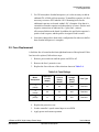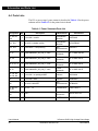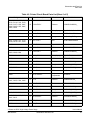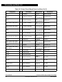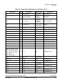
1
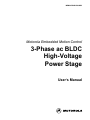
3-Phase ac BLDC
High-Voltage
Power Stage
User’s Manual
N O N - D I S C L O S U R E
Motorola Embedded Motion Control
A G R E E M E N T
R E Q U I R E D
MEMC3PBLDCPSUM/D
Important Notice to Users
While every effort has been made to ensure the accuracy of all information in
this document, Motorola assumes no liability to any party for any loss or
damage caused by errors or omissions or by statements of any kind in this
document, its updates, supplements, or special editions, whether such errors are
omissions or statements resulting from negligence, accident, or any other cause.
Motorola further assumes no liability arising out of the application or use of any
information, product, or system described herein: nor any liability for incidental
or consequential damages arising from the use of this document. Motorola
disclaims all warranties regarding the information contained herein, whether
expressed, implied, or statutory, including implied warranties of
merchantability or fitness for a particular purpose. Motorola makes no
representation that the interconnection of products in the manner described
herein will not infringe on existing or future patent rights, nor do the
descriptions contained herein imply the granting or license to make, use or sell
equipment constructed in accordance with this description.
Trademarks
This document includes these trademarks:
Motorola and the Motorola logo are registered trademarks
of Motorola, Inc.
Motorola, Inc., is an Equal Opportunity / Affirmative Action Employer.
© Motorola, Inc., 2000; All Rights Reserved
User’s Manual
2
3-Phase ac BLDC High-Voltage Power Stage
MOTOROLA
User’s Manual — 3-Phase ac BLDC High-Voltage Power Stage
List of Sections
Section 1. Introduction and Setup . . . . . . . . . . . . . . . . . . 11
Section 2. Operational Description . . . . . . . . . . . . . . . . . 19
Section 3. Pin Descriptions . . . . . . . . . . . . . . . . . . . . . . . 25
Section 4. Schematics and Parts List . . . . . . . . . . . . . . . 31
Section 5. Design Considerations . . . . . . . . . . . . . . . . . . 47
3-Phase ac BLDC High-Voltage Power Stage
MOTOROLA
User’s Manual
List of Sections
3
List of Sections
User’s Manual
4
3-Phase ac BLDC High-Voltage Power Stage
List of Sections
MOTOROLA
User’s Manual — 3-Phase ac BLDC High-Voltage Power Stage
Table of Contents
Section 1. Introduction and Setup
1.1
Contents . . . . . . . . . . . . . . . . . . . . . . . . . . . . . . . . . . . . . . . . . . . . . . . 11
1.2
Introduction. . . . . . . . . . . . . . . . . . . . . . . . . . . . . . . . . . . . . . . . . . . . . 11
1.3
About this Manual. . . . . . . . . . . . . . . . . . . . . . . . . . . . . . . . . . . . . . . . 13
1.4
Warnings . . . . . . . . . . . . . . . . . . . . . . . . . . . . . . . . . . . . . . . . . . . . . . . 15
1.5
Setup Guide. . . . . . . . . . . . . . . . . . . . . . . . . . . . . . . . . . . . . . . . . . . . . 16
Section 2. Operational Description
2.1
Contents . . . . . . . . . . . . . . . . . . . . . . . . . . . . . . . . . . . . . . . . . . . . . . . 19
2.2
Description . . . . . . . . . . . . . . . . . . . . . . . . . . . . . . . . . . . . . . . . . . . . . 19
2.3
Electrical Characteristics . . . . . . . . . . . . . . . . . . . . . . . . . . . . . . . . . . 21
2.4
Modification for One-Half and Three-Fourths Horsepower. . . . . . . . 22
2.5
Fuse Replacement . . . . . . . . . . . . . . . . . . . . . . . . . . . . . . . . . . . . . . . . 23
Section 3. Pin Descriptions
3.1
Contents . . . . . . . . . . . . . . . . . . . . . . . . . . . . . . . . . . . . . . . . . . . . . . . 25
3.2
3.2.1
3.2.2
3.2.3
3.2.4
Pin-by-Pin Descriptions . . . . . . . . . . . . . . . . . . . . . . . . . . . . . . . . . . . 25
Power Input Connector J11 . . . . . . . . . . . . . . . . . . . . . . . . . . . . . . 25
Motor Output Connector J13 . . . . . . . . . . . . . . . . . . . . . . . . . . . . . 26
External Brake Connector J12 . . . . . . . . . . . . . . . . . . . . . . . . . . . . 26
40-Pin Ribbon Connector J14 . . . . . . . . . . . . . . . . . . . . . . . . . . . . 27
3-Phase ac BLDC High-Voltage Power Stage
MOTOROLA
User’s Manual
Table of Contents
5
Table of Contents
Section 4. Schematics and Parts List
4.1
Contents . . . . . . . . . . . . . . . . . . . . . . . . . . . . . . . . . . . . . . . . . . . . . . . 31
4.2
Mechanical Characteristics . . . . . . . . . . . . . . . . . . . . . . . . . . . . . . . . . 31
4.3
Schematics . . . . . . . . . . . . . . . . . . . . . . . . . . . . . . . . . . . . . . . . . . . . . 31
4.4
Parts Lists . . . . . . . . . . . . . . . . . . . . . . . . . . . . . . . . . . . . . . . . . . . . . . 40
Section 5. Design Considerations
5.1
Contents . . . . . . . . . . . . . . . . . . . . . . . . . . . . . . . . . . . . . . . . . . . . . . . 47
5.2
Overview. . . . . . . . . . . . . . . . . . . . . . . . . . . . . . . . . . . . . . . . . . . . . . . 47
5.3
3-Phase H-Bridge . . . . . . . . . . . . . . . . . . . . . . . . . . . . . . . . . . . . . . . . 48
5.4
Bus Voltage and Current Feedback . . . . . . . . . . . . . . . . . . . . . . . . . . 50
5.5
Cycle-by-Cycle Current Limiting . . . . . . . . . . . . . . . . . . . . . . . . . . . . 52
5.6
Temperature Sensing . . . . . . . . . . . . . . . . . . . . . . . . . . . . . . . . . . . . . 54
5.7
Back EMF Signals . . . . . . . . . . . . . . . . . . . . . . . . . . . . . . . . . . . . . . . 55
5.8
Phase Current Sensing . . . . . . . . . . . . . . . . . . . . . . . . . . . . . . . . . . . . 56
5.9
Brake . . . . . . . . . . . . . . . . . . . . . . . . . . . . . . . . . . . . . . . . . . . . . . . . . . 57
5.10
Power Factor Correction . . . . . . . . . . . . . . . . . . . . . . . . . . . . . . . . . . . 58
User’s Manual
6
3-Phase ac BLDC High-Voltage Power Stage
Table of Contents
MOTOROLA
User’s Manual — 3-Phase ac BLDC High-Voltage Power Stage
List of Figures
Figure
Title
1-1
1-2
1-3
1-4
Systems’ Configurations. . . . . . . . . . . . . . . . . . . . . . . . . . . . . . . . . . . 13
3-Phase ac BLDC High-Voltage Power Stage . . . . . . . . . . . . . . . . . . 14
Setup . . . . . . . . . . . . . . . . . . . . . . . . . . . . . . . . . . . . . . . . . . . . . . . . . . 17
PFC Jumper. . . . . . . . . . . . . . . . . . . . . . . . . . . . . . . . . . . . . . . . . . . . . 18
2-1
Block Diagram . . . . . . . . . . . . . . . . . . . . . . . . . . . . . . . . . . . . . . . . . . 20
3-1
40-Pin Ribbon Connector J14. . . . . . . . . . . . . . . . . . . . . . . . . . . . . . . 27
4-1
4-2
4-3
4-4
4-5
4-6
4-7
4-8
3-Phase ac BLDC High-Voltage Power Stage Overview. . . . . . . . . . 32
Gate Drive. . . . . . . . . . . . . . . . . . . . . . . . . . . . . . . . . . . . . . . . . . . . . . 33
3-Phase H-Bridge . . . . . . . . . . . . . . . . . . . . . . . . . . . . . . . . . . . . . . . . 34
Current and Temperature Feedback . . . . . . . . . . . . . . . . . . . . . . . . . . 35
Back EMF Signals . . . . . . . . . . . . . . . . . . . . . . . . . . . . . . . . . . . . . . . 36
Power Factor Correction and Brake Gate Drives . . . . . . . . . . . . . . . . 37
Power Supply . . . . . . . . . . . . . . . . . . . . . . . . . . . . . . . . . . . . . . . . . . . 38
Identification Block . . . . . . . . . . . . . . . . . . . . . . . . . . . . . . . . . . . . . . 39
5-1
5-2
5-3
5-4
5-5
5-6
5-7
5-8
5-9
Phase A Output . . . . . . . . . . . . . . . . . . . . . . . . . . . . . . . . . . . . . . . . . . 49
Bus Feedback . . . . . . . . . . . . . . . . . . . . . . . . . . . . . . . . . . . . . . . . . . . 51
Cycle-by-Cycle Current Limiting . . . . . . . . . . . . . . . . . . . . . . . . . . . . 53
Temperature Sensing . . . . . . . . . . . . . . . . . . . . . . . . . . . . . . . . . . . . . 54
Phase A Back EMF. . . . . . . . . . . . . . . . . . . . . . . . . . . . . . . . . . . . . . . 55
Phase A Current Sensing . . . . . . . . . . . . . . . . . . . . . . . . . . . . . . . . . . 56
Brake . . . . . . . . . . . . . . . . . . . . . . . . . . . . . . . . . . . . . . . . . . . . . . . . . . 58
PFC Circuitry . . . . . . . . . . . . . . . . . . . . . . . . . . . . . . . . . . . . . . . . . . . 59
PFC Zero Crossing Feedback . . . . . . . . . . . . . . . . . . . . . . . . . . . . . . . 60
3-Phase ac BLDC High-Voltage Power Stage
MOTOROLA
Page
User’s Manual
List of Figures
7
List of Figures
User’s Manual
8
3-Phase ac BLDC High-Voltage Power Stage
List of Figures
MOTOROLA
User’s Manual — 3-Phase ac BLDC High-Voltage Power Stage
List of Tables
Table
Title
2-1
2-2
2-3
2-4
Electrical Characteristics . . . . . . . . . . . . . . . . . . . . . . . . . . . . . . . . . . 21
Resistor Values . . . . . . . . . . . . . . . . . . . . . . . . . . . . . . . . . . . . . . . . . . 22
JP801 Settings. . . . . . . . . . . . . . . . . . . . . . . . . . . . . . . . . . . . . . . . . . . 22
Fuse Ratings . . . . . . . . . . . . . . . . . . . . . . . . . . . . . . . . . . . . . . . . . . . . 23
3-1
3-2
Connector J13 Signal Descriptions . . . . . . . . . . . . . . . . . . . . . . . . . . 26
Connector J14 Signal Descriptions . . . . . . . . . . . . . . . . . . . . . . . . . . 28
4-1
4-2
Power Substrate Parts List . . . . . . . . . . . . . . . . . . . . . . . . . . . . . . . . . 40
Printed Circuit Board Parts List . . . . . . . . . . . . . . . . . . . . . . . . . . . . . 41
3-Phase ac BLDC High-Voltage Power Stage
MOTOROLA
Page
User’s Manual
List of Tables
9
List of Tables
User’s Manual
10
3-Phase ac BLDC High-Voltage Power Stage
List of Tables
MOTOROLA
User’s Manual — 3-Phase ac BLDC High-Voltage Power Stage
Section 1. Introduction and Setup
1.1 Contents
1.2
Introduction. . . . . . . . . . . . . . . . . . . . . . . . . . . . . . . . . . . . . . . . . . . . . 11
1.3
About this Manual. . . . . . . . . . . . . . . . . . . . . . . . . . . . . . . . . . . . . . . . 13
1.4
Warnings . . . . . . . . . . . . . . . . . . . . . . . . . . . . . . . . . . . . . . . . . . . . . . . 15
1.5
Setup Guide. . . . . . . . . . . . . . . . . . . . . . . . . . . . . . . . . . . . . . . . . . . . . 16
1.2 Introduction
Motorola’s 3-Phase ac high-voltage brushless dc (BLDC) power stage (HV ac
power stage) is a 115/230 volt, 180 watt (one-fourth horsepower), off-line
power stage that is an integral part of Motorola’s embedded motion control
series of development tools. It is supplied in kit number ECPWRHiVACBLDC.
In combination with one of the embedded motion control series control boards
and an embedded motion control series optoisolation board, it provides a
ready-made software development platform for fractional horsepower off-line
motors. Feedback signals are provided that allow 3-phase ac induction and
BLDC motors to be controlled with a wide variety of algorithms. In addition,
the HV ac power stage includes an active power factor correction (PFC) circuit
that facilitates development of PFC algorithms.
An illustration of the systems’ architecture is shown in Figure 1-1. A line
drawing appears in Figure 1-2.
3-Phase ac BLDC High-Voltage Power Stage
MOTOROLA
User’s Manual
Introduction and Setup
11
Introduction and Setup
The HV ac power stage’s features are:
•
1-phase bridge rectifier
•
Power factor switch and diode
•
dc-bus brake IGBT and brake resistors
•
3-phase bridge inverter (6-IGBT’s)
•
Individual phase and dc bus current sensing shunts with Kelvin
connections
•
Power stage temperature sensing diodes
•
IGBT gate drivers
•
Current and temperature signal conditioning
•
3-phase back-EMF voltage sensing and zero cross detection circuitry
•
Board identification processor (MC68HC705JJ7)
•
Low-voltage on-board power supplies
•
Cooling fans
User’s Manual
12
3-Phase ac BLDC High-Voltage Power Stage
Introduction and Setup
MOTOROLA
Introduction and Setup
About this Manual
EMULATOR
CONTROL BOARD
DSP EVM BOARD
WORKSTATION
WORKSTATION
OPTOISOLATION
BOARD
OPTOISOLATION
BOARD
HIGH-VOLTAGE
POWER STAGE
HIGH-VOLTAGE
POWER STAGE
MOTOR
a) MICROCONTROLLER
MOTOR
b) 56800 DSP
Figure 1-1. Systems’ Configurations
1.3 About this Manual
Key items can be found in the following locations in this manual:
•
Setup instructions are found in 1.5 Setup Guide.
•
Schematics are found in Section 4. Schematics and Parts List.
•
Pin assignments are shown in Figure 3-1. 40-Pin Ribbon Connector
J14, and a pin-by-pin description is contained in 3.2 Pin-by-Pin
Descriptions.
•
For those interested in the reference design aspects of the board’s
circuitry, a description is provided in Section 5. Design Considerations.
3-Phase ac BLDC High-Voltage Power Stage
MOTOROLA
User’s Manual
Introduction and Setup
13
N D I S
C
User’s Manual – 3 Phase AC BLDC High Voltage Power Stage
N
O
Figure 1-2. 3 Phase AC BLDC High Voltage Power Stage
Introduction and Setup
Warnings
1.4 Warnings
This development tool set operates in an environment that includes dangerous
voltages and rotating machinery.
To facilitate safe operation, input power for the HV ac power stage should come
from a current limited dc laboratory power supply, unless power factor
correction is specifically being investigated.
An isolation transformer should be used when operating off an ac power line.
If an isolation transformer is not used, power stage grounds and oscilloscope
grounds are at different potentials, unless the oscilloscope is floating. Note that
probe grounds and, therefore, the case of a floated oscilloscope are subjected to
dangerous voltages.
The user should be aware that:
•
Before moving scope probes, making connections, etc., it is generally
advisable to power down the high-voltage supply.
•
When high voltage is applied, using only one hand for operating the test
setup minimizes the possibility of electrical shock.
•
Operation in lab setups that have grounded tables and/or chairs should be
avoided.
•
Wearing safety glasses, avoiding ties and jewelry, using shields, and
operation by personnel trained in high-voltage lab techniques are also
advisable.
•
Power transistors, the PFC coil, and the motor can reach temperatures hot
enough to cause burns.
•
When powering down; due to storage in the bus capacitors, dangerous
voltages are present until the power-on LED is off.
3-Phase ac BLDC High-Voltage Power Stage
MOTOROLA
User’s Manual
Introduction and Setup
15
Introduction and Setup
1.5 Setup Guide
Setup and connections for the HV ac power stage are straightforward. The
power stage connects to an embedded motion control optoisolation board via a
40-pin ribbon cable and can be powered either by a 140- to 230-volt dc power
supply or with line voltage. For both safety reasons and ease of making
measurements, it is strongly recommended that a dc supply is used, unless
power factor correction is specifically being investigated. The power supply
should be current limited to under 4 amps. Figure 1-3 depicts a completed
setup. A step-by-step setup procedure is:
1. Plug one end of the 40-pin ribbon cable that comes with the optoisolator
kit into input connector J14. The other end of this cable goes to the
optoisolation board's 40-pin output connector.
2. Connect motor leads to output connector J13, located along the back
edge of the top board. Phase A, phase B, and phase C are labeled Ph_A,
Ph_B, and Ph_C.
For an ac induction motor, it does not matter which lead goes to which
phase. For BLDC motors, it is important to get the wire color coded for
phase A into the connector terminal labeled Ph_A, and so on for phase B
and phase C.
3. Connect earth ground to the earth ground terminals on the top board and
on the heat sink. The top board’s ground terminal is located in the front
left-hand corner and is marked with a ground symbol. The heat sink has
a screw on its front edge that is also marked with a ground symbol.
4. Connect a line isolated, current limited dc power supply to connector
J11, located on the front edge of the top board. The input voltage range
is 140 to 230 Vdc. Current limit should be set for less than 4 amps. The
dc supply’s polarity does not matter.
Either a 110-volt or 220-volt ac line that is coupled through an isolation
transformer may be used in place of a dc supply to provide input power.
The connection is made on connector J11. Bias voltages are developed
by internal power supplies. Only one power input is required.
WARNING:
Operation off an ac power line is significantly more hazardous than operation
from a line isolated and current limited dc power supply.
An isolation transformer should be used when operating off an ac power line.
User’s Manual
16
3-Phase ac BLDC High-Voltage Power Stage
Introduction and Setup
MOTOROLA
Introduction and Setup
Setup Guide
5. Set up the optoisolation and control boards.
6. Optional PFC — The HV ac power stage is shipped with power factor
correction (PFC) disabled. If power factor correction is desired, it is
necessary to remove and resolder power jumper JP201 from the no PFC
position to the PFC position. This jumper is found on the left side of the
top board between the dc bus capacitor and PFC inductor. Circuit
connections are illustrated in Figure 1-4. For first time setups, operation
without power factor correction is recommended.
7. Apply power first to the optoisolator and then to the power stage. The
green power-on LED in the upper right-hand corner lights, and both fans
run when power is present. Note that the optoisolation board powers the
control board, and that the optoisolation board is not fully powered until
power is applied to the power stage.
CAUTION:
Hazardous voltages are present. Re-read all of 1.4 Warnings carefully.
MOTOR
STANDOFFS
40-PIN
RIBBON CABLE
+12 Vdc
CONTROL BOARD
POWER STAGE
OPTOISOLATOR
40-PIN
RIBBON CABLE
J1
J2
STANDOFFS
HIGH-VOLTAGE
MOTOR SUPPLY
Figure 1-3. Setup
3-Phase ac BLDC High-Voltage Power Stage
MOTOROLA
User’s Manual
Introduction and Setup
17
Introduction and Setup
L201
PFC
1
DCB_PFC_1
3
DCB_PFC_2
4.9 mH/2.3 A
2 JP201
PFC JUMPER
NO PFC
DCB_Cap_pos
C213
10 nF/3000 V
C208
22 nF/630 Vdc
Earth_GND
+
C209
470 µF/400 V
+
C210
470 µF/400 V
(OPTIONAL)
C214
10 nF/3000 V
DCB_Cap_neg
Figure 1-4. PFC Jumper
User’s Manual
18
3-Phase ac BLDC High-Voltage Power Stage
Introduction and Setup
MOTOROLA
User’s Manual — 3-Phase ac BLDC High-Voltage Power Stage
Section 2. Operational Description
2.1 Contents
2.2
Description . . . . . . . . . . . . . . . . . . . . . . . . . . . . . . . . . . . . . . . . . . . . . 19
2.3
Electrical Characteristics . . . . . . . . . . . . . . . . . . . . . . . . . . . . . . . . . . 21
2.4
Modification for One-Half and Three-Fourths Horsepower. . . . . . . . 22
2.5
Fuse Replacement . . . . . . . . . . . . . . . . . . . . . . . . . . . . . . . . . . . . . . . . 23
2.2 Description
Motorola’s embedded motion control series high-voltage (HV) ac power stage
is a 180 watt (one-fourth horsepower), 3-phase power stage that will operate
off of dc input voltages from 140 to 230 volts and ac line voltages from 100 to
240 volts. In combination with one of the embedded motion control series
control boards and an optoisolation board, it provides a software development
platform that allows algorithms to be written and tested without the need to
design and build a power stage. It supports a wide variety of algorithms for both
ac induction and brushless dc (BLDC) motors.
Input connections are made via 40-pin ribbon cable connector J14. Pin
assignments for the input connector are shown in Figure 3-1. 40-Pin Ribbon
Connector J14. Power connections to the motor are made on output connector
J13. Phase A, phase B, and phase C are labeled PH_A, Ph_B, and Ph_C on the
board. Power requirements are met with a single external 140- to 230-volt dc
power supply or an ac line voltage. Either input is supplied through connector
J11. Current measuring circuitry is set up for 2.93 amps full scale. Both bus and
phase leg currents are measured. A cycle-by-cycle overcurrent trip point is set
at 2.69 amps.
3-Phase ac BLDC High-Voltage Power Stage
MOTOROLA
Operational Description
User’s Manual
19
Operational Description
The high-voltage ac power stage has both a printed circuit board and a power
substrate. The printed circuit board contains IGBT gate drive circuits, analog
signal conditioning, low-voltage power supplies, power factor control circuitry,
and some of the large, passive, power components. This board also has an
MC68HC705JJ7 microcontroller that is used for configuration and
identification. All of the power electronics which need to dissipate heat are
mounted on the power substrate. This substrate includes the power IGBTs,
brake resistors, current sensing resistors, a power factor correction MOSFET,
and temperature sensing diodes. Figure 2-1 shows a block diagram.
HV POWER
INPUT
SWITCH MODE
POWER SUPPLY
PFC CONTROL
dc BUS BRAKE
3-PHASE IGBT
POWER MODULE
SIGNALS
TO/FROM
CONTROL
BOARD
3-PHASE AC
TO
MOTOR
GATE
DRIVERS
PHASE CURRENT
PHASE VOLTAGE
BUS CURRENT
BUS VOLTAGE
MONITOR
BOARD
ID BLOCK
ZERO CROSS
BACK-EMF SENSE
Figure 2-1. Block Diagram
User’s Manual
20
3-Phase ac BLDC High-Voltage Power Stage
Operational Description
MOTOROLA
Operational Description
Electrical Characteristics
2.3 Electrical Characteristics
The electrical characteristics in Table 2-1 apply to operation at 25°C with a
160-Vdc power supply voltage.
Table 2-1. Electrical Characteristics
Characteristic
Symbol
Min
Typ
Max
Units
dc input voltage
Vdc
140
160
230
V
ac input voltage
Vac
100
208
240
V
Quiescent current
ICC
—
70
—
mA
Min logic 1 input voltage
VIH
2.0
—
—
V
Max logic 0 input voltage
VIL
—
—
0.8
V
Input resistance
RIn
—
10 kΩ
—
Analog output range
VOut
0
—
3.3
V
Bus current sense voltage
ISense
—
563
—
mV/A
Bus voltage sense voltage
VBus
—
8.09
—
mV/V
Peak output current
IPK
—
—
2.8
A
Brake resistor dissipation
(continuous)
PBK
—
—
50
W
Brake resistor dissipation
(15 sec pk)
PBK(Pk)
—
—
100
W
Pdiss
—
—
85
W
Total power dissipation
3-Phase ac BLDC High-Voltage Power Stage
MOTOROLA
Operational Description
User’s Manual
21
Operational Description
2.4 Modification for One-Half and Three-Fourths Horsepower
The HV ac power stage can be modified for operation at either one-half or
three-fourths horsepower. To change maximum output power, follow these
steps:.
1. Remove power and wait until the power-on LED is off.
2. If PFC jumper JP201 is in the PFC position, remove and resolder it into
the no PFC position.
3. Make the resistor value changes shown in Table 2-2. These resistors set
current amplifier gains. For one-half and three-fourths horsepower,
lower gains allow for higher measured currents and higher overcurrent
trip points.
Table 2-2. Resistor Values
1/ HP
4
1/ HP
2
3/ HP
4
(180 W)
(370 W)
(550 W)
R303, R305, R307, R314, R315, R318,
R319, R322
75 kΩ
62 kΩ
56 kΩ
R301, R304, R311, R313, R316, R317,
R320, R321
10 kΩ
15 kΩ
16 kΩ
Resistors
4. Configure identification coding jumper JP801 with the settings indicated
in Table 2-3. This proceedure allows software to interpret the new
analog values correctly.
Table 2-3. JP801 Settings
1/ HP
4
1/ HP
2
3/ HP
4
(180 W)
(370 W)
(550 W)
1-2
Open
Short
Open
3-4
Open
Open
Short
5-6
Open
Open
Open
7-8
Open
Open
Open
Position
User’s Manual
22
3-Phase ac BLDC High-Voltage Power Stage
Operational Description
MOTOROLA
Operational Description
Fuse Replacement
5. For 550 watts (three-fourths horsepower), it is also necessary to add an
addional 470-µF/400-volt bus capacitor. To install the capacitor, it is first
necessary to remove PFC inductor L201. Mounting holes for the
additional capacitor are located within L201’s footprint. Note that it is
essential to orient the capacitor such that polarity is correct. Positive and
negative connections are indicated by + (plus) and – (minus)
silk-screened labels on the board. In addition, the pad for the capacitor’s
positive lead is square, and the pad for its negative lead is round.
6. Once these changes have been made, configuration for either one-half or
three-fourths horsepower is complete.
2.5 Fuse Replacement
A fast blow fuse is located on the front right-hand corner of the top board. If this
fuse has to be replaced, follow these steps:
1. Remove power and wait until the power-on LED is off.
2. Remove the fuse’s protective case.
3. Replace the fuse with one of the selections shown in Table 2-4.
Table 2-4. Fuse Ratings
Motor
Horsepower
1/
4
(180 W)
1/
2
(370 W)
3/
4
(550 W)
RMS Input
Current
(Amps)
Fuse
Current
Rating
(Amps)
Fuse
Voltage
Rating
(Volts)
Fuse Type
2.3
2.5
250
Fast blow
4.8
6.3
250
Fast blow
7.1
8
250
Fast blow
4. Replace the protective case.
5. Set the controller’s speed control input to zero RPM.
6. Apply power and resume operation.
3-Phase ac BLDC High-Voltage Power Stage
MOTOROLA
Operational Description
User’s Manual
23
Operational Description
User’s Manual
24
3-Phase ac BLDC High-Voltage Power Stage
Operational Description
MOTOROLA
User’s Manual — 3-Phase ac BLDC High-Voltage Power Stage
Section 3. Pin Descriptions
3.1 Contents
3.2
3.2.1
3.2.2
3.2.3
3.2.4
Pin-by-Pin Descriptions . . . . . . . . . . . . . . . . . . . . . . . . . . . . . . . . . . . 25
Power Input Connector J11 . . . . . . . . . . . . . . . . . . . . . . . . . . . . . . 25
Motor Output Connector J13 . . . . . . . . . . . . . . . . . . . . . . . . . . . . . 26
External Brake Connector J12 . . . . . . . . . . . . . . . . . . . . . . . . . . . . 26
40-Pin Ribbon Connector J14 . . . . . . . . . . . . . . . . . . . . . . . . . . . . 27
3.2 Pin-by-Pin Descriptions
Inputs and outputs are located on four connectors. Pin descriptions for each of
these connectors are included in this section.
3.2.1 Power Input Connector J11
The power input connector, labeled J11, is located on the front edge of the
board. It will accept dc voltages from 140 to 230 volts or an isolated ac line
input from 100 to 240 volts. In either case, the power source should be capable
of supplying at least 200 watts.
3-Phase ac BLDC High-Voltage Power Stage
MOTOROLA
User’s Manual
Pin Descriptions
25
Pin Descriptions
3.2.2 Motor Output Connector J13
Power outputs to the motor are located on connector J11. Phase outputs are
labeled Ph_A, Ph_B, and Ph_C. Pin assignments are described in Table 3-1.
Table 3-1. Connector J13 Signal Descriptions
Pin
No.
Signal Name
1
2
3
Description
Ph_A
Ph_A supplies power to motor phase A. On an induction motor, any one of the
three phase windings can be connected here. For brushless dc motors it is
important to connect the wire color coded for phase A into the connector terminal
labeled Ph_A, and so on for phase B and phase C.
Ph_B
Ph_B supplies power to motor phase B. On an induction motor, any one of the
three phase windings can be connected here. For brushless dc motors it is
important to connect the wire color coded for phase B into the connector terminal
labeled Ph_B, and so on for phase A and phase C.
Ph_C
Ph_C supplies power to motor phase C. On an induction motor, any one of the
three phase windings can be connected here. For brushless dc motors it is
important to connect the wire color coded for phase C into the connector terminal
labeled Ph_C, and so on for phase A and phase B.
3.2.3 External Brake Connector J12
An optional external brake resistor can be connected to external brake connector
J12, labeled Ext. Brake. The external resistor allows power dissipation to
increase beyond the 50 watts that brake resistors R6–R9 provide.
User’s Manual
26
3-Phase ac BLDC High-Voltage Power Stage
Pin Descriptions
MOTOROLA
Pin Descriptions
Pin-by-Pin Descriptions
3.2.4 40-Pin Ribbon Connector J14
Signal inputs are grouped together on 40-pin ribbon cable connector J14,
located on the right side of the board. Pin assignments are shown in Figure 3-1.
In this figure, a schematic representation appears on the left, and a physical
layout of the connector appears on the right. The physical view assumes that
the board is oriented such that its title is read from left to right. Signal
descriptions are listed in Table 3-2.
J14
BEMF_sense_C
BEMF_sense_B
BEMF_sense_A
Shielding
Zero_cross_C
Zero_cross_B
Zero_cross_A
PFC_z_c
PFC_inhibit
PFC_PWM
Serial_Con
Brake_control
Shielding
Temp_sense
I_sense_C
I_sense_B
I_sense_A
I_sense_DCB
V_sense_DCB
–15V_A
+15V_A
GNDA
GNDA
+3.3V_A
+5V_D
+5V_D
GND
GND
PWM_CB
Shielding
PWM_CT
Shielding
PWM_BB
Shielding
PWM_BT
Shielding
PWM_AB
Shielding
PWM_AT
40
39
38
37
36
35
34
33
32
31
30
29
28
27
26
25
24
23
22
21
20
19
18
17
16
15
14
13
12
11
10
9
8
7
6
5
4
3
2
1
PWM_AT
PWM_AB
PWM_BT
PWM_BB
PWM_CT
PWM_CB
GND_PS
+5V_D
GNDA
+15V_A
V_sense_DCB
I_sense_A
I_sense_C
Brake_control
PFC_PWM
PFC_z_c
Zero_cross_B
Shielding
BEMF_sense_B
1
3
5
7
9
11
13
15
17
19
21
23
25
27
29
31
33
35
37
39
2
4
6
8
10
12
14
16
18
20
22
24
26
28
30
32
34
36
38
40
Shielding
Shielding
Shielding
Shielding
Shielding
GND
+5V_D
+3.3V_A
GNDA
–15V_A
I_sense_DCB
I_sense_B
Temp_sense
Shielding
Serial_Con
PFC_inhibit
Zero_cross_A
Zero_cross_C
BEMF_sense_A
BEMF_sense_C
PHYSICAL VIEW
SCHEMATIC VIEW
CON40
Figure 3-1. 40-Pin Ribbon Connector J14
3-Phase ac BLDC High-Voltage Power Stage
MOTOROLA
User’s Manual
Pin Descriptions
27
Pin Descriptions
Table 3-2. Connector J14 Signal Descriptions
Pin
No.
Signal Name
1
PWM_AT
PWM_AT is the gate drive signal for the top half-bridge of phase A. A logic high
turns phase A’s top switch on.
2
Shielding
Pin 2 is connected to a shield wire in the ribbon cable and ground on the board.
3
PWM_AB
PWM_AB is the gate drive signal for the bottom half-bridge of phase A. A logic high
turns phase A’s bottom switch on.
4
Shielding
Pin 4 is connected to a shield wire in the ribbon cable and ground on the board.
5
PWM_BT
PWM_BT is the gate drive signal for the top half-bridge of phase B. A logic high
turns phase B’s top switch on.
6
Shielding
Pin 6 is connected to a shield wire in the ribbon cable and ground on the board.
7
PWM_BB
PWM_BB is the gate drive signal for the bottom half-bridge of phase B. A logic high
turns phase B’s bottom switch on.
8
Shielding
Pin 8 is connected to a shield wire in the ribbon cable and ground on the board.
9
PWM_CT
PWM_CT is the gate drive signal for the top half-bridge of phase C. A logic high
turns phase C’s top switch on.
10
Shielding
Pin 10 is connected to a shield wire in the ribbon cable and ground on the board.
11
PWM_CB
PWM_CB is the gate drive signal for the bottom half-bridge of phase C. A logic high
turns phase C’s bottom switch on.
12
GND
Digital and power ground
13
GND
Digital and power ground, redundant connection
14
+5V digital
Digital +5-volt power supply
15
+5V digital
Digital +5-volt power supply, redundant connection
16
+3.3V analog
17
GNDA
Analog power supply ground
18
GNDA
Analog power supply ground, redundant connection
19
+15V_A
Analog +15-volt power supply
20
–15V_A
Analog –15-volt power supply
21
V_sense_DCB
V_sense_DCB is an analog sense signal that measures dc bus voltage. It is scaled
at 8.09 mV per volt of dc bus voltage.
22
I_sense_DCB
I_sense_DCB is an analog sense signal that measures dc bus current. It is scaled
at 0.563 volts per amp of dc bus current.
Description
Analog +3.3-volt power supply
User’s Manual
28
3-Phase ac BLDC High-Voltage Power Stage
Pin Descriptions
MOTOROLA
Pin Descriptions
Pin-by-Pin Descriptions
Table 3-2. Connector J14 Signal Descriptions (Continued)
Pin
No.
Signal Name
Description
23
I_sense_A
I_sense_A is an analog sense signal that measures current in phase A. It is scaled
at 0.563 volts per amp of dc bus current.
24
I_sense_B
I_sense_B is an analog sense signal that measures current in phase B. It is scaled
at 0.563 volts per amp of dc bus current.
25
I_sense_C
I_sense_C is an analog sense signal that measures current in phase C. It is scaled
at 0.563 volts per amp of dc bus current.
26
Temp_sense
Temp_sense is an analog sense signal that measures power module temperature.
27
No connection
Pin 28 is connected to a shield wire in the ribbon cable and analog ground on the
board.
28
Shielding
29
Brake_control
30
Serial_Con
Serial_Con is an identification signal that lets the controller know which power
stage is present.
31
PFC_PWM
PFC_PWM is a digital signal that controls the power factor correction circuit’s
switch.
32
PFC_inhibit
PFC_inhibit is a digital output used to enable or disable the power factor correction
circuit.
33
PFC_z_c
34
Zero_cross_A
Zero_cross_A is a digital signal used for sensing phase A back-EMF zero crossing
events.
35
Zero_cross_B
Zero_cross_B is a digital signal used for sensing phase B back-EMF zero crossing
events.
36
Zero_cross_C
Zero_cross_C is a digital signal used for sensing phase C back-EMF zero crossing
events.
37
Shielding
Pin 37 is connected to a shield wire in the ribbon cable and analog ground on the
board.
38
BEMF_sense_A
BEMF_sense_A is an analog sense signal that measures phase A back EMF. It is
scaled at 8.09 mV per volt of dc bus voltage.
39
BEMF_sense_B
BEMF_sense_B is an analog sense signal that measures phase B back EMF. It is
scaled at 8.09 mV per volt of dc bus voltage.
40
BEMF_sense_C
BEMF_sense_A is an analog sense signal that measures phase C back EMF. It is
scaled at 8.09 mV per volt of dc bus voltage.
Brake_control is the gate drive signal for the brake IGBT.
PFC_z_c is a digital signal. Its edges represent power line voltage zero crossing
events.
3-Phase ac BLDC High-Voltage Power Stage
MOTOROLA
User’s Manual
Pin Descriptions
29
Pin Descriptions
User’s Manual
30
3-Phase ac BLDC High-Voltage Power Stage
Pin Descriptions
MOTOROLA
User’s Manual — 3-Phase ac BLDC High-Voltage Power Stage
Section 4. Schematics and Parts List
4.1 Contents
4.2
Mechanical Characteristics . . . . . . . . . . . . . . . . . . . . . . . . . . . . . . . . . 31
4.3
Schematics . . . . . . . . . . . . . . . . . . . . . . . . . . . . . . . . . . . . . . . . . . . . . 31
4.4
Parts Lists . . . . . . . . . . . . . . . . . . . . . . . . . . . . . . . . . . . . . . . . . . . . . . 40
4.2 Mechanical Characteristics
Mechanically, the high-voltage (HV) power stage consists of an FR-4 circuit
board, a 3.2-mm aluminum circuit board, two fans, a fan bracket, a heat sink,
inter-board connectors, and standoffs. Construction is depicted in Figure 1-2.
3-Phase ac BLDC High-Voltage Power Stage. The aluminum circuit board,
fans, and heat sink provide thermal capability for surface-mounted power
components. The FR-4 board contains control circuitry and through-hole
mounted power components. The two boards plug together via 10 vertical
connectors to, in effect, form a discrete power module.
Four holes on the top board are spaced to allow mounting standoffs such that a
control board can be placed on top of the power stage. This configuration allows
mounting control and power functions in one compact mechanical assembly.
4.3 Schematics
A set of schematics for the HV ac power stage appears in Figure 4-1 through
Figure 4-8. An overview of the board appears in Figure 4-1. H-bridge gate
drive is shown in Figure 4-2. The 3-phase H-bridge appears in Figure 4-3.
Current and temperature feedback circuits are shown in Figure 4-4. Back EMF
feedback circuitry appears in Figure 4-5. Power factor correction and brake
gate drives are shown in Figure 4-6. An on-board power supply appears in
Figure 4-7, and finally the identification block is shown in Figure 4-8. Unless
otherwise specified, resistors are 1/8 watt, have a ±5% tolerance, and have
values shown in ohms. Interrupted lines coded with the same letters are
electrically connected.
3-Phase ac BLDC High-Voltage Power Stage
MOTOROLA
Schematics and Parts List
User’s Manual
31
+FAN
-FAN
C1
1
Identification
100nF
+5V_D
+15V_A
+15V_D
+5V_D
FAN 2
Identification
GND
+15V_A
+3.3V_A
+15V_D
+5V_D
GND
-15V_A
GND
+5V_D
+FAN
-FAN
+5V_D
GND
+15V_D
+15V_D
+5V_D
GND
GNDA
BEMF_sense_C
BEMF_sense_B
BEMF_sense_A
Zero_cros_C
Zero_cros_B
Zero_cros_A
Phase_A
Phase_B
Phase_C
Back_EMF
GNDA
V_sense_DCB_half_15
GNDA
-FAN
+FAN
+15V_A
-15V_A
+3.3V_A
GND
Power_pos
Power_neg
+5V_D
SMPS
+5V_D
+15V_D
+15V_A
GND
GNDA
DCB_Cap_neg
Earth_GND
DCB_Cap_pos
FAN 2
Brake_gate
1
PFC_I_sense_1
Earth
Ground
PFC_gate
PFC_Source
100nF
DCB_PFC_1
DCB_PFC_2
V_sense_DCB_5
V_sense_DCB_half_15
C2
PFC_z_c
PFC_enable
PFC_PWM
Brake_control
PFC_DC_BUS_BRAKE
GNDA
FAN1
+15V_D
GNDA
J15
GND
FAN2
Temp_sense_2
GNDA
Brake
1
2
GNDA
-15V_A
+15V_A
17
18
19
20
9
10
11
12
1
2
3
4
4
5
6
POWER
MODULE
4
5
6
J5
CON/C
1
J6
CON/C
4
5
6
1
J7
CON/C
1
1
2
3
4
5
6
J8
CON/E
J2
CON/A
4
5
6
J10
CON/B
D1
V14E250
1
2
3
4
J9
CON/E
J4
CON/C
1
J3
CON/B
1
2
3
4
J1
CON/A
1
2
3
4
5
6
4
3
2
1
20
19
18
17
12
11
10
9
J12
GNDA
Motor
Terminals
J13
1
2
3
+15V_D
+3.3V_A
+3.3V_A
GND
GND
I_T_Processing
PWM_CB
PWM_CT
PWM_BB
PWM_BT
PWM_AB
PWM_AT
GND
+5V_D
Gate_BT
Source_BT
+15V_D
I_sense_C2
I_sense_C1
Temp_sense_1
Temp_sense_2
Phase_A
Phase_B
Phase_C
HV_Drivers
+15V_D +5V_D
Shut_Down_Open C.
Temp_sense
I_sense_C
I_sense_B
I_sense_A
I_sense_DCB
+15V_D
GNDA
GNDA
I_sense_B2
I_sense_B1
Line
Input
I_sense_A2
I_sense_A1
I_sense_DCB2
I_sense_DCB1
2
1
J11
Gate_CT
Source_CT
Source_CB
Gate_CB
Source_BB
Gate_BB
Source_AB
Gate_AB
F1
2.5A/250V
Fast-Blow
Gate_AT
Source_AT
i
Shut_Down
R1
R/ivar SG-190
GND
Temp_sense_2
GNDA
Figure 4-1. 3 Phase AC BLDC High Voltage Power Stage Overview
+3.3V_A
+5V_D
GND
J14
40
39
38
37
36
35
34
33
32
31
30
29
28
27
26
25
24
23
22
21
20
19
18
17
16
15
14
13
12
11
10
9
8
7
6
5
4
3
2
1
BEMF_sense_C
BEMF_sense_B
BEMF_sense_A
Sheilding
Zero_cross_C
Zero_cross_B
Zero_cross_A
PFC_z_c
PFC_enable
PFC_PWM
Serial_Con
Brake_control
Shielding
Temp_sense
I_sense_C
I_sense_B
I_sense_A
I_sense_DCB
V_sense_DCB
PWM_CB
Shielding
PWM_CT
Shielding
PWM_BB
Shielding
PWM_BT
Shielding
PWM_AB
Shielding
PWM_AT
D402
U404A
DM74ALS1034M
1
PWM_AT
3
PWM_AB
Gate_AT
+5V_D
C402
4.7uF/16V
2
C401
100nF
4
9
10
11
12
13
14
15
16
GND
C420
1nF
U404B
DM74ALS1034M
n/c
n/c
VDD
HIN
SD
LIN
VSS
n/c
IR2112S
+15V_D
D403
MMSZ5251BT1
Source_AT
+
D404
C416
33uF/25V
MBRS130LT3
Gate_AB
C404
470nF/50V
R402
120
GND
D405
MMSZ5251BT1
Source_AB
C413 8.2pF
Shut_Down
R404
10k
HO
VB
VS
n/c
n/c
VCC
COM
LO
8
7
6
5
4
3
2
1
R401
120
R414
10k
R413
R403
10k
D401
MBRS130LT3
C403
470nF/50V
U401
+
+5V_D
C419
1nF
MBRS130LT3
+5V_D
MBRS130LT3
D406
100
GND
U404C
DM74ALS1034M
5
PWM_BT
6
9
PWM_BB
Gate_BT
+5V_D
C406
4.7uF/16V
C405
100nF
U402
+
8
9
10
11
12
13
14
15
16
C422
1nF
HO
VB
VS
n/c
n/c
VCC
COM
LO
IR2112S
GND
C421
1nF
n/c
n/c
VDD
HIN
SD
LIN
VSS
n/c
D408
MBRS130LT3
C407
470nF/50V
8
7
6
5
4
3
2
1
R405
120
+15V_D
D407
MMSZ5251BT1
Source_BT
D409
+ C417
33uF/25V
Gate_BB
C408
470nF/50V
U404D
DM74ALS1034M
MBRS130LT3
R406
120
GND
D410
MMSZ5251BT1
C414 8.2pF
Source_BB
+5V_D
R407
10k
R408
10k
D411
GND
U404E
DM74ALS1034M
11
PWM_CT
10
13
PWM_CB
Gate_CT
+5V_D
C410
4.7uF/16V
C409
100nF
12
C424
1nF
9
10
11
12
13
14
15
16
n/c
n/c
VDD
HIN
SD
LIN
VSS
n/c
HO
VB
VS
n/c
n/c
VCC
COM
LO
IR2112S
U404F
DM74ALS1034M
+5V_D
R412
10k
GND
+15V_D
+15V_D
VCC
+5V_D
VCC
10nF
C425
+5V_D
8
7
6
5
4
3
2
1
GND
GND
GND
Figure 4-2. Gate Drive
R409
120
+15V_D
D412
MMSZ5251BT1
Source_CT
+
C418
33uF/25V
MBRS130LT3
D414
Gate_CB
C412
470nF/50V
GND
C415 8.2pF
R411
10k
D413
MBRS130LT3
C411
470nF/50V
U403
+
GND
C423
1nF
MBRS130LT3
R410
120
D415
MMSZ5251BT1
Source_CB
DCB_PFC_1
DCB_Cap_Pos
D12
DCB_PFC_2
Q1
SKB10N60
HFA08TB60S
D7
10ETS08S
D8
10ETS08S
R8
250
R6
250
MTB8N50E
AC_IN_L1
Gate_AT
Q8
D11
HFA08TB60S
R9
250
R7
250
Brake_Res
AC_IN_L2
Q3
SKB10N60
Gate_CT
Gate_BT
Phase_B
Phase_A
Q5
SKB10N60
Phase_C
Q2
SKB10N60
Q4
SKB10N60
Q6
SKB10N60
Gate_AB
Gate_BB
Gate_CB
Source_AB
Source_BB
Source_CB
Gate_PFC
Source_PFC
D9
10ETS08S
D10
10ETS08S
Q7
SGB10N60
I_sense_A1
Gate_Brake
I_sense_A2
DCB_Cap_Neg
I_sense_B1
R1
0.075 1%
sense
I_sense_B2
sense
R2
0.075 1%
sense
sense
I_sense_C1
R3
0.075 1%
sense
I_sense_C2
sense
sense
R4
0.075 1%
sense
sense
R5
0.075 1%
sense
D13
D14
BAV99LT1
BAV99LT1
Temp_sense1
I_Sense_PFC1
I_Sense_DCB1
I_Sense_PFC2
I_Sense_DCB2
J8
SM/CON/MCRD_SR_500_E - male
J9
SM/CON/MCRD_SR_500_E - male
J10
SM/CON/MCRD_SR_500_B - male
Figure 4-3. 3 Phase H-Bridge
J6
SM/CON/MCRD_SR_500_C - male
Phase_C
4
5
6
Gate_CT
1
Phase_B
4
5
6
Gate_BT
1
Gate_AT
Brake_Res
Phase_A
4
5
6
1
J5
SM/CON/MCRD_SR_500_C - male
I_Sense_DCB2
I_Sense_DCB1
Gate_AB
Source_AB
I_sense_A2
I_sense_A1
J4
SM/CON/MCRD_SR_500_C - male
1
2
3
4
5
6
Gate_BB
Source_BB
I_sense_B2
I_sense_B1
J3
SM/CON/MCRD_SR_500_B - male
4
5
6
1
Gate_Brake
Gate_PFC
Source_PFC
Temp_sense2
I_Sense_PFC2
Temp_sense1
I_Sense_PFC1
1
2
3
4
5
6
DCB_Cap_Neg
17
18
19
20
DCB_PFC_2
9
10
11
12
DCB_Cap_Pos
J2
SM/CON/MCRD_SR_500_A - male
1
2
3
4
1
2
3
4
Gate_CB
Source_CB
I_sense_C2
I_sense_C1
J1
SM/CON/MCRD_SR_500_A - male
1
2
3
4
AC_IN_L2
17
18
19
20
AC_IN_L1
9
10
11
12
1
2
3
4
DCB_PFC_1
Temp_sense2
J7
SM/CON/MCRD_SR_500_C - male
+15V_D
+15V_D
+3.3V_A
+3.3V_A
8
GNDA
GND
GND
R303 75k-1%
3
+
2
-
R301 10k-1%
7
+
R304 10k-1%
I_sense_A
GNDA
Temp_sense_2
1
Temp_sense
C301
100nF
Temp_sense_1
(1.65V +/- 1.65V @ +/- Imax)
GND
U302B
MC33502D
1.65V ref
R305
75k-1%
2.21k-1%
LM393D
-
5
I_sense_A2
R306 680k
Over-current
Detection
R307 75k-1%
R308
1.2k
+15V_D
R309
1.2k
R311 10k-1%
2
-
3
C303
680pF
1
R313 10k-1%
8
R314
75k-1%
+3.3V_A
R310
470
GNDA
I_sense_B
(1.65V +/- 1.65V @ +/- Imax)
+
I_sense_B2
GNDA
U301A
MC33502D
+
6
-
7
R315 75k-1%
DC Bus Current
Sensing
C304
100nF
I_sense_DCB
4
R316 10k-1%
R318 75k-1%
I_sense_DCB1
2
I_sense_DCB2
3
GNDA
R317 10k-1%
R322
75k-1%
+
R321 10k-1%
-
5
I_sense_C2
7
I_sense_C
(1.65V +/- 1.65V @ +/- Imax)
U301B
MC33502D
C305
100nF
1.65V ref
GNDA
+
C306
3.3uF/10V
5
R325
33.2k-1%
4
LM285M
U304
GNDA
R324
100k-1%
8
C307
100nF
I_sense_DCB
(1.65V +/- 1.65V @ +/- Imax)
U302A
MC33502D
+3.3V_A
R319
75k-1%
R323 390
+3.3V_A
1
8
R320 10k-1%
6
Shut_Down_Open C.
GND
GNDA
I_sense_C1
U303B
LM393D
R312
10k
GNDA
+3.3V_A
1.65V ref
5
4
4
I_sense_DCB
I_sense_B1
R302
U303A
4
6
I_sense_A1
Temperature
Sensing
+15V_D
8
GND
Phase Current
Sensing
+
C302
10nF
GNDA
-
+3.3V_A
GNDA
Figure 4-4. Current & Temperature Feedback
R501
Phase_A
324k-1%
(400V max)
R502
274k-1%
+5V_D
R504
215k-1%
R505
10k
R506
9
0
R507
21.0k-1%
8
+
-
C501
10pF
BEMF_sense_A
(3.24V @ Phase_A = 400V)
+15V_D
+15V_D
+5V_D
+5V_D
GND
GND
14
Zero_cross_A
GNDA
U501C
LM339D
GNDA
R508
6.81k-1%
GNDA
R509
Phase_B
GNDA
324k-1%
(400V max)
R510
374k-1%
+15V_D
C503
+5V_D
10nF
3
R512
215k-1%
R514
0
R515
21.0k-1%
+
4
-
C502
10pF
12
BEMF_sense_B
(3.24V @ Phase_B = 400V)
5
R513
10k
GND
2
Zero_cross_B
U501A
LM339D
+5V_D
R516
6.81k-1%
GND
11
+
10
-
GNDA
C506
R517
10nF
Phase_C
(400V max)
GNDA
324k-1%
GND
GND
R519
374k-1%
+5V_D
R520
215k-1%
R521
10k
R522
0
R523
21.0k-1%
BEMF_sense_C
(3.24V @ Phase_C = 400V)
C504
10pF
7
+
6
-
1
U501B
LM339D
V_sense_DCB_half_15
R524
6.81k-1%
(6.60V @ Vbus = 400V)
C505
22pF
GNDA
GNDA
GNDA
Figure 4-5. Back EMF Signals
Zero_cross_C
13
U501D
LM339D
+5V_D
PFC_I_sense_1
VCC
+5V_D
+15V_D
+15V_D
+15V_A
+15V_A
C204
10nF
+15V_A
C202
10uF/35V
R206 100k
R205
GND
GNDA
R203
68-1%
+5V_D
+
+15V_D
1k-1%
+15V_D
C206
10nF
C201
6.8nF
C207
22nF
U201A
1
3
2
PFC_PWM
R201
R209
3.92k-1%
10k-1%
MC74VHCT00AD
R212
680-1%
R214
3.3k
U202
1 NC
GND
3
+
2
-
U201B
1
4
PFC_gate
33
VCC
NC
8
D202
MMSZ5251BT1
R213
10k
U201C
6
LM393D
U203A
R210
C203
100nF GND
8
C205
R207
12.1k-1%
GND
PFC Switch
R208
10k
9
8
2 InA
OutA
7
R211
10k
4 InB
OutB
5
5
PFC_Source
10
4
GND
6
22nF
GNDA
GND
MC74VHCT00AD
MC74VHCT00AD
R204
Brake_gate
100
GND
MC33152D
3
Brake Switch
Brake_control
PFC_enable
R202
10k
D201
MMSZ5251BT1
GND
GND
GNDA
GND
GND
C212
1nF
GND
R215
10k
GND
+15V_D
+15V_D
GND
+5V_D
+15V_D
2
L201
R219
1
R220
JP201
PFC Jumper
3
33k
4.9mH/2.3A
33k
5
+
6
-
33k
R222
10k
R223
10k
R218
4.7k
7
PFC_z_c
LM393D
U203B
GND
Bus Voltage Feedback
DCB_Cap_pos
V_sense_DCB_half_15
274k-1%
R224
C213
10nF/3000V
+
C208
22nF/630VDC
C214
10nF/3000V
ref_l = 11.81V
ref_h = 11.86V
R221
DCB_PFC_2
no PFC
Earth_GND
R217
2.7k
4
PFC Option:
PFC
D203
SM/1N4148
C211
1nF
8
Zero Crossing
Detection
DCB_PFC_1
R216 270k
C209
470uF/400V
274k-1%
R225
4.87k-1%
R226
274k-1%
R227
GNDA
GNDA
R228
6.81k-1%
R229
255-1%
V_sense_DCB
(3.235V @ Vbus = 400V)
U201D
12
R230
6.81k-1%
11
13
DCB_Cap_neg
MC74VHCT00AD
GNDA
Figure 4-6. Power Factor Correction & Brake Gate Drives
GND
Power_pos
Power_neg
+3.3V_A
+5V_D
FB
GND
+5V_D
+15V_D
-15V_A
-15V_A
C100
10pF/500V
D100
R100
1.0k
GNDA
D102
GNDA
MURS160T3
GND
R101
1.0k
GND
+FAN
+FAN
-FAN
-FAN
+
1
Power_pos
+15V_A
C128
10uF/6.3V
R102
1.0k
R103
1.0k
GND
+
3
+
12
2
11
3
10
4
9
5
8
6
7
D103
R104
270
2
3
1
4
U100
SFH6106
R105
R106
2.21k-1%
D110 MBR0530T1
+17V_D
C107
MBRS1100T3
C116
100nF
Drain
1
R108
6.8
1
U101
TL431BCD
+
Control
+
GNDA C112
100nF
C113
C129
33uF/25V
33uF/25V
3
10
4
9
TOP202YAI
D112
D111
R113
27
R112
27
5
8
6
7
TNY254P
1
+FAN
C123
100nF
2
C124
100pF/500V
Drain
S
S
S
S
EN
S
3
6
7
8
3
U104
SFH6106
VIN VOUT
2 3
6 7
1
+15V_D
C127
100nF
C122
100uF/16V
GND
-FAN
D107
MMSZ5242BT1
R115
330
2
R114
1.0k
4
+17V_D
+5V_D
5
4
8
C126
100nF
U103
BP
MBR0530T1
MBR0530T1
U108
MC78L15ACD
+
R111
27
C114
100nF
1
U102
D106
MBRS1100T3
T101
SM/Trafo_EFD15/12PIN
1
12
11
Vin Gnd
Vin
Vin Vout
Vin
2
47uF/16V
2
7
6
3
2
U107
MC79L15ACD
GND
R110
27
C110
100nF
Source
+ C117
Power_pos
C109
MBRS1100T3
3
3
2
+ C108
+15V_A
1
5
D105
7
6
+
VIN VOUT
2 3
6 7
GND
GND
R109
2.21k-1%
U106
MC78L15ACD
8
33uF/25V
GNDA
GNDA
C111
33uF/25V
820
8
C105
100nF
100nF
MBRS1100T3
+ C104
GC101
Ground_Connection
C102
C103 GND
220uF/10V 220uF/10V
D104
+3.3V_A
10uF/6.3V
D108
MMSZ5231BT1
33uF/25V
+
-CE
+
C101
220uF/10V
SM/Trafo_EFD20/12PIN
FB
U110
MC78PC33NTR
5
Vin Vout
1
3
T100
P6SMB200AT3
+15V_D
+15V_A
+5V_D
4
GND
+3.3V_A
D109 MBR0530T1
D101
MBRD660CT
1
2
Power_pos
1
D113
GREEN LED
C125 1nF/1kV
GND
GND
Figure 4-7. Power Supply
GND
-15V_A
+5V_D
C801 +
10uF/6.3V
+5V_D
C802
10nF
U801
MC68HC705JJ7DW_MOD
18
GND
11
12
13
Identification
R801
GND
VCC
PA2
PA1
PA0
PA3
PA4
PA5
19
+5V_D
R802 R803
10k
10k
10
9
8
JP801
10k
14
15
16
17
+5V_D
X801
0
R804 R805
10k
10k
20
IRQ
RESET
OSC2
OSC1
PB0
4MHz
PB7
PB6
PB5
PB4/TCMP
PB3/TCAP
PB2/AN2
PB1/AN1
7
6
5
4
3
2
1
8
6
4
2
3
2
1
Coding bit #
Coding bit #
7
6
5
4
7
5
3
1
SM/JUMPER4x2
GND
Coding bit #
GND
+5V_D
+5V_D
DEFAULT SETTINGS:
0 - PTB0 = H
1 - PTB1 = H
2 - PTB2 = H
3 - PTB3 = H
4 - PTB4 = H
5 - PTB5 = H
6 - PTA6 = H
7 - PTA7 = H
+5V_D
GND
GND
Figure 4-8. Identification Block
Schematics and Parts List
4.4 Parts Lists
The HV ac power stage’s parts content is described in Table 4-1 for the power
substrate and in Table 4-2 for the printed circuit board.
Table 4-1. Power Substrate Parts List
Designators
Qty
Description
Manufacturer
Part Number
D7, D8, D9,
D10
4
10 A/800 V rectifier
International
Rectifier
10ETS08S
D11, D12
2
8 A/600 V ultrafast rectifier
International
Rectifier
HFA08TB60S
D13, D14
2
Dual diode — temp sensing
ON
Semiconductor
BAV99LT1
J1, J2
2
SM/CON/MCRD_SR_500_A - male
Fisher
Elektronik
SL 11 SMD 104 20Z
J3, J10
2
SM/CON/MCRD_SR_500_B - male
Fisher
Elektronik
SL 10 SMD 104 6Z
J4, J5, J6, J7
4
SM/CON/MCRD_SR_500_C - male
Fisher
Elektronik
SL 10 SMD 104 6Z
J8, J9
2
SM/CON/MCRD_SR_500_E - male
Fisher
Elektronik
SL 10 SMD 104 4Z
Q1, Q2, Q3,
Q4, Q5, Q6
6
10 A/600 V co-packaged IGBT
Infineon
SKB10N60
Q7
1
10 A/600 V IGBT
Infineon
SGB10N60
Q8
1
8 A/500 V MOSFET
ON
Semiconductor
MTB8N50E
R1, R2, R3,
R4, R5
5
0.075 Ω 1%
Isabellenhutte
PMA-A-R075-1
R6, R7, R8,
R9
4
250 Ω
Caddock
Electronics
MP725-250-5.0%
1
Power substrate
CUBE
46615770
User’s Manual
40
3-Phase ac BLDC High-Voltage Power Stage
Schematics and Parts List
MOTOROLA
Schematics and Parts List
Parts Lists
Table 4-2. Printed Circuit Board Parts List (Sheet 1 of 5)
Designators
Qty
Description
Manufacturer
C1, C2, C105, C109, C110,
C112, C114, C116, C123,
C126, C127, C203, C301,
C304, C305, C307, C401,
C405, C409
19
100 nF/25 V
Vitramon
VJ0805U104MXXA_
C100
1
10 pF/500 V
Vishay Sprague
Typ:5GAQ10, Serie: 562C
C101, C102, C103
3
220 µF/10 V
AVX
TPSE227K010R0100
C104,C128,C801
3
10 µF/6.3 V
Sprague
293D106X_6R3B2_
C107, C108, C111, C113,
C129, C416, C417, C418
8
33 µF/25 V
AVX
TPSE336K025R0200
C117
1
47 µF/16 V
Any available
C122
1
100 µF/16 V
AVX
TPSE107K016R0100
C204, C206, C302, C425,
C503, C506, C802
7
10 nF/25 V
Vitramon
VJ0805U103MXXA_
C124
3
100 pF/500 V
Vishay Sprague
Typ:5GAT10, Serie: 562C
C125
1
1 nF/1 kV
muRata
DE0505E102Z1K
C201
1
6.8 nF
Vitramon
VJ0805A682JXA_
C202
1
10 µF/35 V
Sprague
293D106X_035D2_
C205, C207
2
22 nF
Vitramon
VJ0805A223JXA_
C208
1
22 nF/630 Vdc
WIMA
MKP10
C209
1
470 µF/400 V
Philips
Components
15746471
C211, C212, C419, C420,
C421, C422, C423, C424
8
1 nF
Vitramon
VJ0805A102JXA_
C213, C214
2
10 nF/ 3000 V
Thomson
5ST410MCMCA
C303
1
680 pF
Vitramon
VJ0805A681JXA_
C306
1
3.3 µF/10 V
Sprague
293D335X_010A2_
C402, C406, C410
3
4.7 µF/16 V
Sprague
293D475X_016B2_
C403, C404, C407, C408,
C411, C412
6
470 nF/50 V
Vitramon
VJ1206U474MXAA_
C413, C414, C415
3
8.2 pF
Vitramon
VJ0805A8R2DXA_
C505
1
22 pF
Vitramon
VJ0805A220DXA_
3-Phase ac BLDC High-Voltage Power Stage
MOTOROLA
Schematics and Parts List
Part Number
User’s Manual
41
Schematics and Parts List
Table 4-2. Printed Circuit Board Parts List (Sheet 2 of 5)
Designators
Qty
Description
Manufacturer
Part Number
D1
1
V14E250
EPCOS
SOIV-S-10K250
D100
1
Transient suppressor
ON
Semiconductor
P6SMB200AT3
D101
1
6 A/60 V Schottky
ON
Semiconductor
MBRD660CT
D102, D401, D408, D413
4
1 A/600 V ultrafast
ON
Semiconductor
MURS160T3
D103, D104, D105, D106
4
1 A/100 V Schottky
ON
Semiconductor
MBRS1100T3
D107
1
12 V/.5 W zener
ON
Semiconductor
MMSZ5242BT1
D108
1
5.1 V/.5 W zener
ON
Semiconductor
MMSZ5231BT1
D109, D110, D111, D112
4
0.5 A/30 V Schottky
ON
Semiconductor
MBR0530T1
D113
1
Green LED
Kingbright
L-934GT
D201, D202, D403, D405,
D407, D410, D412, D415
8
22 V/0.5 W zener
ON
Semiconductor
MMSZ5251BT1
D203
1
1N4148
Fairchild
1N4148LL-34
D402, D404, D406, D409,
D411, D414
6
1 A/30 V Schottky
ON
Semiconductor
MBRS130LT3
F1
1
Fuse holder
MULTICOMP
MCHTE15M
JP201
1
Power jumper
JP801
1
4X2 jumper pads
J2, J1
2
20-pin connector
Fisher
Elektronik
BL 2 20Z
J3, J10
2
6-pin connector
Fisher
Elektronik
BL 1 6Z
J4, J5, J6, J7
4
6-pin connector
Fisher
Elektronik
BL 1 6Z
J9, J8
2
4-pin connector
Fisher
Elektronik
BL 1 4Z
J11, J12
2
Terminal block
Weidmuller
LP 7.62/2/90
User’s Manual
42
3-Phase ac BLDC High-Voltage Power Stage
Schematics and Parts List
MOTOROLA
Schematics and Parts List
Parts Lists
Table 4-2. Printed Circuit Board Parts List (Sheet 3 of 5)
Designators
Qty
Description
Manufacturer
Part Number
J13
1
Terminal block
Weidmuller
LP 7.62/3/90
J14
1
40-pin connector
Fischer
Elektronik
ASLG40G
L201
1
4.9 mH/2.3 A
Thompson
Television
Components
SMT4 ref G6982
R1
1
Inrush limiter
Rhopoint
Components
SG190
R100, R101, R102, R103
4
1.0 kΩ
Dale
CRCW1206-102J
R104
1
270 Ω
Dale
CRCW0805-271J
R105
1
820 Ω
Dale
CRCW0805-821J
R106, R109
2
2.21 kΩ –1%
Any available
R108
1
56 Ω
Any available
R110, R111, R112, R113
4
27 Ω
Dale
CRCW1206-270J
R114
1
1.0 kΩ
Dale
CRCW0805-102J
R115
1
330 Ω
Dale
CRCW0805-331J
R201
1
3.92 kΩ –1%
Any available
R202, 214
2
3.3 kΩ
Dale
CRCW0805-332J
R208, R211, R213, R215,
R223, R312, R403, R404,
R407, R408, R411, R412,
R414, R505, R513, R521,
R801, R802
R803, R804, R805
21
10 kΩ
Dale
CRCW0805-103J
R203
1
68.1 –1%
Any available
R204, R413
2
100 Ω
Dale
CRCW0805-101J
R206
1
100 kΩ
Dale
CRCW0805-104J
R207
1
12.1 kΩ –1%
Any available
R210
1
33 Ω
Dale
R212
1
681 Ω –1%
Any available
R216
1
270 Ω
Dale
CRCW0805-274J
R217
1
2.7 kΩ
Dale
CRCW0805-272J
3-Phase ac BLDC High-Voltage Power Stage
MOTOROLA
Schematics and Parts List
CRCW0805-330J
User’s Manual
43
Schematics and Parts List
Table 4-2. Printed Circuit Board Parts List (Sheet 4 of 5)
Designators
Qty
Description
Manufacturer
Part Number
R218
1
4.7 kΩ
Dale
CRCW0805-472J
R219
1
33 kΩ
Dale
CRCW0805-333J
R220, R221
2
33 kΩ
Dale
CRCW0805-333J
R222
1
10 kΩ
Dale
CRCW0805-103J
R224, R225, R227, R502,
R510, R519
6
274 kΩ –1%
Any available
R226
1
4.87 kΩ –1%
Any available
R228, R230, R508, R516,
R524
5
6.81 kΩ–1%
Any available
R229
1
255 Ω –1%
Any available
R209, R301, R304, R311,
R313, R316, R317, R320,
R321
9
10 kΩ –1%
Dale
R302
1
2.21 kΩ –1%
Any available
R205
1
1 kΩ –1%
Dale
CRCW0805-102F
R303, R305, R307, R314,
R315, R318, R319, R322
8
75 kΩ –1%
Dale
CRCW0805-753F
R306
1
680 kΩ
Dale
CRCW0805-684J
R308, R309
2
1.2 kΩ
Dale
CRCW0805-122J
R310
1
220 Ω
Dale
CRCW0805-221J
R323
1
390 Ω
Dale
CRCW0805-391J
R324
1
100 kΩ –1%
Dale
CRCW0805-104F
R325
1
33.2 kΩ –1%
Any available
R401, R402, R405, R406,
R409, R410
6
120 Ω
Dale
R501, R509, R517
3
324 kΩ –1%
Any available
R504, R512, R520
3
215 kΩ –1%
Any available
R506, R514, R522
3
0
Any available
R507, R515, R523
3
21.0 kΩ –1%
Any available
T100
1
SMPS transformer
Tronic Praha
s.r.o
User’s Manual
44
CRCW0805-103F
CRCW0805-121J
TRONIC 99 060 09
3-Phase ac BLDC High-Voltage Power Stage
Schematics and Parts List
MOTOROLA
Schematics and Parts List
Parts Lists
Table 4-2. Printed Circuit Board Parts List (Sheet 5 of 5)
Designators
Qty
Description
Manufacturer
Part Number
T101
1
SMPS transformer
Tronic Praha
s.r.o
TRONIC 00 003 73
U100, U104
2
Optocoupler
Infineon
SFH6106-2
U101
1
Voltage reference
ON
Semiconductor
TL431BCD
U102
1
SMPS controller
Power
Integration
TOP202YAI
U103
1
SMPS controller
Power
Integration
TNY254P
U108, U106
2
15 V/.1 A regulator
ON
Semiconductor
MC78L15ACD
U107
1
– 15 V/0.1 A regulator
ON
Semiconductor
MC79L15ACD
U110
1
3.3 V/.15 A regulator
ON
Semiconductor
MC78PC33NTR
U201
1
Quad 2-input NAND gate
ON
Semiconductor
MC74VHCT00AD
U202
1
Dual gate driver
ON
Semiconductor
MC33152D
U203, U303
2
Dual comparator
ON
Semiconductor
LM393D
U301, U302
2
Dual op amp
ON
Semiconductor
MC33502D
U304
1
Voltage reference
National
Semiconductor
LM285M
U401, U402, U403
3
Dual gate driver
International
Rectifier
IR2112S
U404
1
Hex non-inverting driver
Fairchild
DM74ALS1034M
U501
1
Quad comparator
ON
Semiconductor
LM339D
U801
1
Microcontroller
Motorola
MC68HC708JJ7CDW
X801
1
4-MHz resonator
muRata
CSTCC4.00MG
3-Phase ac BLDC High-Voltage Power Stage
MOTOROLA
Schematics and Parts List
User’s Manual
45
Schematics and Parts List
User’s Manual
46
3-Phase ac BLDC High-Voltage Power Stage
Schematics and Parts List
MOTOROLA
User’s Manual — 3-Phase ac BLDC High-Voltage Power Stage
Section 5. Design Considerations
5.1 Contents
5.2
Overview. . . . . . . . . . . . . . . . . . . . . . . . . . . . . . . . . . . . . . . . . . . . . . . 47
5.3
3-Phase H-Bridge . . . . . . . . . . . . . . . . . . . . . . . . . . . . . . . . . . . . . . . . 48
5.4
Bus Voltage and Current Feedback . . . . . . . . . . . . . . . . . . . . . . . . . . 50
5.5
Cycle-by-Cycle Current Limiting . . . . . . . . . . . . . . . . . . . . . . . . . . . . 52
5.6
Temperature Sensing . . . . . . . . . . . . . . . . . . . . . . . . . . . . . . . . . . . . . 54
5.7
Back EMF Signals . . . . . . . . . . . . . . . . . . . . . . . . . . . . . . . . . . . . . . . 55
5.8
Phase Current Sensing . . . . . . . . . . . . . . . . . . . . . . . . . . . . . . . . . . . . 56
5.9
Brake . . . . . . . . . . . . . . . . . . . . . . . . . . . . . . . . . . . . . . . . . . . . . . . . . . 57
5.10
Power Factor Correction . . . . . . . . . . . . . . . . . . . . . . . . . . . . . . . . . . . 58
5.2 Overview
From a systems point of view, the HV ac power stage fits into an architecture
that is designed for software development. In addition to the hardware that is
needed to run a motor, a variety of feedback signals that facilitate control
algorithm development and a PFC circuit are provided.
Circuit descriptions for the HV ac power stage appear in 5.3 3-Phase H-Bridge
through 5.10 Power Factor Correction. One phase leg of the 3-phase H-bridge
is looked at in 5.3 3-Phase H-Bridge. Bus voltage and bus current feedback are
discussed in 5.4 Bus Voltage and Current Feedback. Cycle-by-cycle current
limiting is highlighted in 5.5 Cycle-by-Cycle Current Limiting. Temperature
sensing is discussed in 5.6 Temperature Sensing. Back-EMF signals appear in
5.7 Back EMF Signals. Phase current sensing is discussed in 5.8 Phase
Current Sensing. The brake is highlighted in 5.9 Brake, and finally power
factor correction is discussed in 5.10 Power Factor Correction.
3-Phase ac BLDC High-Voltage Power Stage
MOTOROLA
User’s Manual
Design Considerations
47
Design Considerations
5.3 3-Phase H-Bridge
The output stage is configured as a 3-phase H-bridge with IGBT output
transistors. It is simplified considerably by high-voltage integrated gate drivers
that have a cycle-by-cycle current limit feature. A schematic that shows one
phase is illustrated in Figure 5-1.
At the input, pulldown resistors R403 and R404 set a logic low in the absence
of a signal. Open input pulldown is important, since it is desirable to keep the
power transistors off in case of either a broken connection or absence of power
on the control board. The drive signal is buffered by U404A and U404B. This
part has a minimum logic 1 input voltage of 2.0 volts and a maximum logic 0
input voltage of 0.8 volts, which allows for inputs from either 3.3- or 5-volt
logic. Gate drive is supplied by an international rectifier, IR2112. Undervoltage
lockout and cycle-by-cycle current limiting are also provided by the IR2112.
Undervoltage lockout is set nominally at 8.4 volts. Current limiting is discussed
further in 5.5 Cycle-by-Cycle Current Limiting.
One of the more important design decisions in a motor drive is selection of gate
drive impedance for the output transistors. In Figure 5-1, resistor R402, diode
D404, and the IR2112’s nominal 500-mA current sinking capability determine
gate drive impedance for the lower half-bridge transistor. A similar network is
used on the upper half-bridge. These networks set turn-on gate drive impedance
at approximately 120 ohms and turn-off gate drive to approximately 500 mA.
These values produce transition times of approximately 200 ns.
Transition times of this length represent a carefully weighed compromise
between power dissipation and noise generation. Generally, transition times
longer than 250 ns tend to get power hungry at non-audible PWM rates; and
transition times under 50 ns create di/dt’s so large that proper operation is
difficult to achieve. The HV ac power stage is designed with switching times at
the higher end of this range to minimize noise.
Anti-parallel diode softness is also a first order design consideration. If the
anti-parallel diodes in an off-line motor drive are allowed to snap, the resulting
di/dt’s can cause noise management problems that are difficult to solve. In
general, it is desirable to have peak to zero di/dt approximately equal the applied
di/dt that is used to turn the anti-parallel diodes off. The SKB10N60 IGBT’s
that are used in this design are targeted at this kind of reverse recovery
characteristic.
User’s Manual
48
3-Phase ac BLDC High-Voltage Power Stage
Design Considerations
MOTOROLA
DCB_Cap_Pos
D402
+5V_D
U404A
DM74ALS1034M
1
PWM_AT
3
PWM_AB
2
C402
4.7uF/16V
C401
100nF
U401
9
10
11
12
13
14
15
16
+
4
GND
n/c
n/c
VDD
HIN
SD
LIN
VSS
n/c
D401
MBRS130LT3
C403
470nF/50V
HO
VB
VS
n/c
n/c
VCC
COM
LO
IR2112S
8
7
6
5
4
3
2
1
C404
470nF/50V
GND
C419
1nF
C420
1nF
R403
10k
R404
10k
U404B
DM74ALS1034M
R401
120
+15V_D
+
C416
33uF/25V
Q1
SKB10N60
MBRS130LT3
D404
D403
MMSZ5251BT1
Q2
SKB10N60
MBRS130LT3
R402
120
D405
MMSZ5251BT1
+5V_D
R414
10k
I_sense_A1
sense
GND
I_sense_A2
R413
C413 8.2pF
+5V_D
Shut_Down
100
Figure 5-1. Phase A Output
I_Sense_DCB2
sense
R1
0.075 1%
Design Considerations
5.4 Bus Voltage and Current Feedback
Feedback signals proportional to bus voltage and bus current are provided by
the circuitry shown in Figure 5-2. Bus voltage is scaled down by a voltage
divider consisting of R224 –R230.
The values are chosen such that a 400-volt maximum bus voltage corresponds
to 3.24 volts at output V_sense_DCB. An additional output,
V_sense_DCB_half_15, provides a reference used in zero crossing detection.
Bus current is sampled by resistor R4 in Figure 4-3, and amplified by the circuit
in Figure 5-2. This circuit provides a voltage output suitable for sampling with
A/D (analog-to-digital) inputs. An MC33502 is used for the differential
amplifier. With R315 = R319 and R316 = R317, the gain is given by:
A = R315/R316
The output voltage is shifted up by 1.65 V to accommodate both positive and
negative current swings. A ±300-mV voltage drop across the sense resistor
corresponds to a measured current range of ±2.93 amps. In addition to providing
an A/D input, this signal also is used for cycle-by-cycle current limiting. A
discussion of cycle-by-cycle current limiting follows in 5.3 3-Phase H-Bridge.
User’s Manual
50
3-Phase ac BLDC High-Voltage Power Stage
Design Considerations
MOTOROLA
DCB_Cap_pos
V_sense_DCB_half_15
274k-1%
R224
274k-1%
R225
4.87k-1%
R226
DC Bus Voltage
Sensing
274k-1%
R227
R228
6.81k-1%
(6.60V @ DC-Bus = 400V)
R229
255-1%
V_sense_DCB
R230
(3.24V @ DC-Bus = 400V)
6.81k-1%
GNDA
R315 75k-1%
DC Bus Current
Sensing
4
I_sense_DCB
2
I_sense_DCB2
3
+
I_sense_DCB1
-
R316 10k-1%
GNDA
U302A
MC33502D
8
R317 10k-1%
1
R319
75k-1%
+3.3V_A
R323 390
1.65V ref
+3.3V_A
C305
100nF
+
C306
3.3uF/10V
5
R325
33.2k-1%
4
LM285M
U304
GNDA
R324
100k-1%
8
C307
100nF
GNDA
Figure 5-2. Bus Feedback
GNDA
I_sense_DCB
Design Considerations
5.5 Cycle-by-Cycle Current Limiting
Cycle-by-cycle current limiting is provided by the circuitry illustrated in
Figure 5-3. Bus current feedback signal, I_sense_DCB, is filtered with R308
and C303 to remove spikes, and then compared to a 3.15-volt reference with
U303B. The open collector output of U303B is pulled up by R414. Additional
filtering is provided by C413, C414, and C415. The resulting signal is fed into
the IR2112 gate driver’s shutdown input on all three phases. Therefore, when
bus current exceeds 2.69 amps, all six output transistors are switched off.
The IR2112’s shutdown input is buffered by RS latches for both top and bottom gate drives. Once a shutdown signal is received, the latches hold the gate
drive off for each output transistor, until that transistor’s gate drive signal is
switched low, and then is turned on again. Hence, current limiting occurs on a
cycle-by-cycle basis.
User’s Manual
52
3-Phase ac BLDC High-Voltage Power Stage
Design Considerations
MOTOROLA
Design Considerations
Cycle-by-Cycle Current Limiting
U401
PWM A TOP
PWM A BOTTOM
9
10
11
12
13
14
15
16
N/C
N/C
VDD
HIN
SD
LIN
VSS
N/C
HO
VB
VS
N/C
N/C
VCC
COM
LO
8
7
6
5
4
3
2
1
A TOP OUT
8
7
6
5
4
3
2
1
B TOP OUT
8
7
6
5
4
3
2
1
C TOP OUT
A BOTTOM OUT
IR2112S
C413 8.2 pF
+5V_D
C414 8.2 pF
+5V_D
U402
PWM B TOP
R306 680 kΩ
PWM B BOTTOM
+5V_D
+15V_D
I_sense_DCB
R308
1.2 kΩ
C303
680 pF
8
R309
1.2 kΩ
5
6
+3.3V_A
R310
470 Ω
GNDA
R312
10 kΩ
+
–
U303B
7
R414
10 kΩ
9
10
11
12
13
14
15
16
N/C
N/C
VDD
HIN
SD
LIN
VSS
N/C
HO
VB
VS
N/C
N/C
VCC
COM
LO
B BOTTOM OUT
IR2112S
R413
100 Ω
LM393D
C415 8.2 pF
+5V_D
4
GND
U403
GNDA
PWM C TOP
PWM C BOTTOM
9
10
11
12
13
14
15
16
N/C
N/C
VDD
HIN
SD
LIN
VSS
N/C
HO
VB
VS
N/C
N/C
VCC
COM
LO
C BOTTOM OUT
IR2112S
Figure 5-3. Cycle-by-Cycle Current Limiting
3-Phase ac BLDC High-Voltage Power Stage
MOTOROLA
User’s Manual
Design Considerations
53
Design Considerations
5.6 Temperature Sensing
Cycle-by-cycle current limiting keeps average bus current within safe limits.
Current limiting by itself, however, does not necessarily ensure that a power
stage is operating within safe thermal limits. For thermal protection, the circuit
in Figure 5-4 is used. It consists of four diodes connected in series, a bias
resistor, and a noise suppression capacitor. The four diodes have a combined
temperature coefficient of 8.8 mV/°C. The resulting signal, Temp_sense, is fed
back to an A/D input where software can be used to set safe operating limits.
Due to unit-to-unit variations in diode forward voltage, it is highly desirable to
calibrate this signal. To do so, a value for Temp_sense is read at a known
temperature and then stored in nonvolatile memory. The measured value, rather
than the nominal value, is then used as a reference point for further readings.
+3.3V_A
R302
2.2 kΩ –1%
D14
D13
BAV99LT1
BAV99LT1
Temp_sense
PIN 26, CONNECTOR J14
C301
100 nF
GNDA
Figure 5-4. Temperature Sensing
User’s Manual
54
3-Phase ac BLDC High-Voltage Power Stage
Design Considerations
MOTOROLA
Design Considerations
Back EMF Signals
5.7 Back EMF Signals
Back EMF and zero crossing signals are included to support sensorless
algorithms for brushless dc motors and dead time distortion correction for ac
induction motors. Referring to Figure 5-5, which shows circuitry for phase A,
the raw phase voltage is scaled down by a voltage divider consisting of R501,
R502, R504, R507, and R508. One output from this divider produces back EMF
sense voltage BEMF_sense_A. Resistor values are chosen such that a 400-volt
maximum phase voltage corresponds to a 3.24-volt maximum A/D input. A
zero crossing signal is obtained by comparing motor phase voltage with
one-half the motor bus voltage. Comparator U501C performs this function,
producing zero crossing signal Zero_cross_A.
Phase_A
R501
324 kΩ –1%
R502
274 kΩ –1%
+5V_D
R504
215 kΩ –1%
R506
0 kΩ
8
R507
21 kΩ –1%
C501
10 pF
BEMF_sense_A
3.24 V @ Phase_A = 400 V
9 +
–
R505
10 kΩ
14
U501C
LM339D
Zero_cross_A
GNDA
R508
6.81 kΩ –1%
GNDA
V_sense_DCB_half_15
C505
22 pF
GNDA
Figure 5-5. Phase A Back EMF
3-Phase ac BLDC High-Voltage Power Stage
MOTOROLA
User’s Manual
Design Considerations
55
Design Considerations
5.8 Phase Current Sensing
Lower half-bridge sampling resistors provide phase current information for all
three phases. Since these resistors sample current in the lower phase legs, they
do not directly measure phase current. However, given phase voltages for all
three phases, phase current can be constructed mathematically from the lower
phase leg values. This information can be used in vector control algorithms for
ac induction motors. The measurement circuitry for one phase is shown in
Figure 5-6.
DCB_Cap_Pos
Q1
SKB10N60
Gate_AT
Phase_A
Q2
SKB10N60
Gate_AB
R303 75 kΩ –1%
Source_AB
sense
R1
0.075 Ω –1%
R301 10 kΩ –1%
6
5
sense
R304 10 kΩ –1%
I_Sense_DCB2
+
7
U302B
MC33502D
I_sense_A
R305
75 kΩ –1%
R323 390 Ω
+3.3V_A
C307
100 nF
–
+
C306
3.3 µF/10 V
1.65 Vref
8
R324
100 kΩ –1%
5
LM285M
U304
R325
33 kΩ –1%
GNDA
4
GNDA
Figure 5-6. Phase A Current Sensing
User’s Manual
56
3-Phase ac BLDC High-Voltage Power Stage
Design Considerations
MOTOROLA
Design Considerations
Brake
Referencing the sampling resistors to the negative motor rail makes the
measurement circuitry straightforward and inexpensive. Current is sampled by
resistor R1, and amplified by differential amplifier U302B. This circuit
provides a voltage output suitable for sampling with A/D inputs. An MC33502
is again used for the differential amplifier. With R301 = R302 and
R303 = R305, the gain is given by:
A = R303/R301
The output voltage is shifted up by 1.65 V to accommodate both positive and
negative current swings. A ±300-mV voltage drop across the shunt resistor
corresponds to a measured current range of ±2.69 amps.
5.9 Brake
A brake circuit is included to dissipate re-generative motor energy during
periods of active deceleration or rapid reversal. Under these conditions, motor
back EMF adds to the dc bus voltage. Without a means to dissipate excess
energy, an overvoltage condition could easily occur.
The circuit shown in Figure 5-7 connects R6–R9 across the dc bus to dissipate
energy. Q7 is turned on by software when the bus voltage sensing circuit in
Figure 5-2 indicates that bus voltage could exceed safe levels. On-board power
resistors R6–R9 will safely dissipate up to 50 watts continuously or up to
100 watts for 15 seconds. Additional power dissipation capability can be added
externally via brake connector J12.
3-Phase ac BLDC High-Voltage Power Stage
MOTOROLA
User’s Manual
Design Considerations
57
Design Considerations
+15V_D
C202
10 µF/35 V
+
J12
1
2
C203
100 nF
U202
1 NC
Brake_control
6
VCC
DCB_Cap_Pos
GND
NC
R6
250 Ω
R8
250 Ω
R7
250 Ω
R9
250 Ω
8
2 InA
OutA 7
4 InB
OutB 5
Q7
SGB10N60
R204
100 Ω
R202
10 kΩ
GND
3
C212
1 nF
GND
D11
HFA08TB60S
MC33152D
GND
D201
MMSZ5251BT1
GND
GND
Figure 5-7. Brake
5.10 Power Factor Correction
A power factor correction (PFC) circuit is included to facilitate development of
software that includes PFC control features. The objective of the PFC hardware
and software is to draw sinusoidal current from the ac line, in an attempt to
approach as closely as possible a unity power factor. Without PFC, current is
drawn from the ac line at the peak of the sine wave, when the ac line voltage
exceeds the dc bus voltage. PFC circuitry is illustrated in Figure 5-8.
User’s Manual
58
3-Phase ac BLDC High-Voltage Power Stage
Design Considerations
MOTOROLA
Design Considerations
Power Factor Correction
NO PFC
3
JP201
2
PFC JUMPER
1
PFC
D7
10ETS08S
L201
D12
HFA08TB60S
4.9 mH/2.3 A
C213
10 nF/
3000 V
D8
10ETS08S
MTB8N50E
Q8
AC_IN_L1
AC_IN_L2
C208
22 nF/
630 Vdc
Earth_GND
SENSE
D9
10ETS08S
R213
10 kΩ
D202
MMSZ5251BT1
GND
+15V_D
I_Sense_PFC1
I_Sense_PFC2
U202
1
NC
2 InA
R203
68.1 Ω – 1%
PFC_I_sense_1
+15V_A
R205
1 kΩ –1%
U201A
2
PFC_PWM
R207
12.1 kΩ
6.8 nF – 1%
3
R201
3.92 kΩ
MC74VHCT00AD –1%
R209
10 kΩ
–1%
R214
3.3 kΩ
PFC_enable
8
NC
OutA 7
R210
33 Ω
OutB 5
+5V_D
C206
10 nF
8
3
2
R212
680 Ω –1%
GNDA
GND
4 InB
+15V_D
C205
C207
22 nF
6
VCC
R206 100 kΩ
22 nF
C201
1
+ C210
470 µF/
400 V
(OPTIONAL)
C214
10 nF/
3000 V
SENSE
D10
10ETS08S
R5
0.075 Ω – 1%
+ C209
470 µF/
400 V
GND
1
+
–
LM393D
U203A
MC33152D
R208
10 kΩ
4
GND
3
GND
U201B
5
MC74VHCT00AD
6
9
U201C
10
MC74VHCT00AD
8
R211
10 kΩ
4
GND
GND
R215
10 kΩ
GND
Figure 5-8. PFC Circuitry
Looking toward the top of Figure 5-8, Q8, L201, D12, and the bus capacitors
form a boost power supply. This configuration allows current to be drawn from
the ac line, when line voltage is lower than the dc bus voltage. Pulse-width
modulation is controlled by software and augmented by the analog circuitry in
the lower half of Figure 5-8. Voltage feedback is provided by the bus voltage
sensing circuit in Figure 5-2. A zero crossing feedback signal, PFC_z_c, is also
used and is produced by the circuit in Figure 5-9.
3-Phase ac BLDC High-Voltage Power Stage
MOTOROLA
User’s Manual
Design Considerations
59
Design Considerations
NO PFC
2
3
DCB_Cap_pos
L201
JP201
1 PFC JUMPER
DCB_PFC_2
4.9 mH/2.3 A
PFC
D8
10ETS08S
D7
10ETS08S
AC_IN_L1
AC_IN_L1
D10
10ETS08S
D9
10ETS08S
I_Sense_PFC1
+15V_D
+15V_D
R216 270 kΩ
+5V_D
+15V_D
C211
1 nF
D203
SM/1N4148
R217
2.7 kΩ
R218
4.7 kΩ
8
5
R219
R220
R221
33 kΩ
33 kΩ
33 kΩ
6
R222
47 kΩ
GNDA
R223
10 kΩ
+
–
7
LM393D
U203B
PFC_z_c
4
GNDA
GND
Figure 5-9. PFC Zero Crossing Feedback
In this circuit, R219, R220, and R221 provide a relatively high impedance
connection to the rectified line voltage, and form a .32:1 voltage divider with
R222. D203 clamps the divided down voltage to approximately 15.7 volts.
Comparator U203B then compares this signal to a 11.8-volt reference.
Approximately fifty millivolts of hysteresis is added by R216. The result is a
logic high at output PFC_z_c when the comparator’s input voltage falls below
11.79 volts. This output remains high until 10.84 volts is reached on the next
cycle.
User’s Manual
60
3-Phase ac BLDC High-Voltage Power Stage
Design Considerations
MOTOROLA
Motorola reserves the right to make changes without further notice to any products herein. Motorola makes no warranty, representation or guarantee regarding the suitability of its
products for any particular purpose, nor does Motorola assume any liability arising out of the application or use of any product or circuit, and specifically disclaims any and all liability,
including without limitation consequential or incidental damages. "Typical" parameters which may be provided in Motorola data sheets and/or specifications can and do vary in different
applications and actual performance may vary over time. All operating parameters, including "Typicals" must be validated for each customer application by customer's technical experts.
Motorola does not convey any license under its patent rights nor the rights of others. Motorola products are not designed, intended, or authorized for use as components in systems
intended for surgical implant into the body, or other applications intended to support or sustain life, or for any other application in which the failure of the Motorola product could create a
situation where personal injury or death may occur. Should Buyer purchase or use Motorola products for any such unintended or unauthorized application, Buyer shall indemnify and hold
Motorola and its officers, employees, subsidiaries, affiliates, and distributors harmless against all claims, costs, damages, and expenses, and reasonable attorney fees arising out of,
directly or indirectly, any claim of personal injury or death associated with such unintended or unauthorized use, even if such claim alleges that Motorola was negligent regarding the
design or manufacture of the part. Motorola and
are registered trademarks of Motorola, Inc. Motorola, Inc. is an Equal Opportunity/Affirmative Action Employer.
How to reach us:
USA/EUROPE/Locations Not Listed: Motorola Literature Distribution, P.O. Box 5405, Denver, Colorado 80217. 1-303-675-2140
or 1-800-441-2447. Customer Focus Center, 1-800-521-6274
JAPAN: Motorola Japan Ltd.; SPS, Technical Information Center, 3-20-1, Minami-Azabu, Minato-ku, Tokyo 106-8573 Japan.
81-3-3440-8573
ASIA/PACIFIC: Motorola Semiconductors H.K. Ltd.; Silicon Harbour Centre, 2 Dai King Street, Tai Po Industrial Estate,
Tai Po, N.T., Hong Kong. 852-26668334
HOME PAGE: http://motorola.com/semiconductors/
© Motorola, Inc., 2000
MEMC3PBLDCPSUM/D