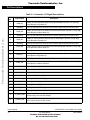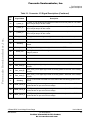
1
Freescale Semiconductor, Inc.
3-Phase BLDC
Low-Voltage
Power Stage
User’s Manual
For More Information On This Product,
Go to: www.freescale.com
A G R E E M E N T
Motorola Embedded Motion Control
N O N - D I S C L O S U R E
Freescale Semiconductor, Inc...
R E Q U I R E D
MEMC3PBLDCLVUM/D
Freescale Semiconductor, Inc.
Important Notice to Users
Freescale Semiconductor, Inc...
While every effort has been made to ensure the accuracy of all information in
this document, Motorola assumes no liability to any party for any loss or
damage caused by errors or omissions or by statements of any kind in this
document, its updates, supplements, or special editions, whether such errors are
omissions or statements resulting from negligence, accident, or any other cause.
Motorola further assumes no liability arising out of the application or use of any
information, product, or system described herein: nor any liability for incidental
or consequential damages arising from the use of this document. Motorola
disclaims all warranties regarding the information contained herein, whether
expressed, implied, or statutory, including implied warranties of
merchantability or fitness for a particular purpose. Motorola makes no
representation that the interconnection of products in the manner described
herein will not infringe on existing or future patent rights, nor do the
descriptions contained herein imply the granting or license to make, use or sell
equipment constructed in accordance with this description.
Trademarks
This document includes these trademarks:
Motorola and the Motorola logo are registered trademarks
of Motorola, Inc.
Motorola, Inc., is an Equal Opportunity / Affirmative Action Employer.
© Motorola, Inc., 2000; All Rights Reserved
User’s Manual
3-Phase BLDC Low-Voltage Power Stage
2
MOTOROLA
For More Information On This Product,
Go to: www.freescale.com
Freescale Semiconductor, Inc.
User’s Manual — 3-Phase BLDC Low-Voltage Power Stage
List of Sections
Section 1. Introduction and Setup . . . . . . . . . . . . . . . . . . 11
Freescale Semiconductor, Inc...
Section 2. Operational Description . . . . . . . . . . . . . . . . . 17
Section 3. Pin Descriptions . . . . . . . . . . . . . . . . . . . . . . . 21
Section 4. Schematics and Parts List . . . . . . . . . . . . . . . 29
Section 5. Design Considerations . . . . . . . . . . . . . . . . . . 43
3-Phase BLDC Low-Voltage Power Stage
MOTOROLA
List of Sections
For More Information On This Product,
Go to: www.freescale.com
User’s Manual
3
Freescale Semiconductor, Inc.
Freescale Semiconductor, Inc...
List of Sections
User’s Manual
4
3-Phase BLDC Low-Voltage Power Stage
List of Sections
For More Information On This Product,
Go to: www.freescale.com
MOTOROLA
Freescale Semiconductor, Inc.
User’s Manual — 3-Phase BLDC Low-Voltage Power Stage
Table of Contents
Freescale Semiconductor, Inc...
Section 1. Introduction and Setup
1.1
Contents . . . . . . . . . . . . . . . . . . . . . . . . . . . . . . . . . . . . . . . . . . . . . . . 11
1.2
Introduction. . . . . . . . . . . . . . . . . . . . . . . . . . . . . . . . . . . . . . . . . . . . . 11
1.3
About this Manual. . . . . . . . . . . . . . . . . . . . . . . . . . . . . . . . . . . . . . . . 13
1.4
Warnings . . . . . . . . . . . . . . . . . . . . . . . . . . . . . . . . . . . . . . . . . . . . . . . 14
1.5
Setup Guide. . . . . . . . . . . . . . . . . . . . . . . . . . . . . . . . . . . . . . . . . . . . . 14
Section 2. Operational Description
2.1
Contents . . . . . . . . . . . . . . . . . . . . . . . . . . . . . . . . . . . . . . . . . . . . . . . 17
2.2
Description . . . . . . . . . . . . . . . . . . . . . . . . . . . . . . . . . . . . . . . . . . . . . 17
2.3
Electrical Characteristics . . . . . . . . . . . . . . . . . . . . . . . . . . . . . . . . . . 19
2.4
Modification for 42 Volts . . . . . . . . . . . . . . . . . . . . . . . . . . . . . . . . . . 19
Section 3. Pin Descriptions
3.1
Contents . . . . . . . . . . . . . . . . . . . . . . . . . . . . . . . . . . . . . . . . . . . . . . . 21
3.2
Introduction. . . . . . . . . . . . . . . . . . . . . . . . . . . . . . . . . . . . . . . . . . . . . 21
3.3
3.3.1
3.3.2
3.3.3
3.3.4
3.3.5
Signal Descriptions . . . . . . . . . . . . . . . . . . . . . . . . . . . . . . . . . . . . . . . 22
40-Pin Ribbon Connector J13 . . . . . . . . . . . . . . . . . . . . . . . . . . . . 22
Power Connectors J19 and J20 . . . . . . . . . . . . . . . . . . . . . . . . . . . 26
Motor Connectors J16, J17, and J18 . . . . . . . . . . . . . . . . . . . . . . . 26
External Brake Connectors J14 and J15 . . . . . . . . . . . . . . . . . . . . 26
Bias Power Connectors J21 and J22 . . . . . . . . . . . . . . . . . . . . . . . 27
3-Phase BLDC Low-Voltage Power Stage
MOTOROLA
Table of Contents
For More Information On This Product,
Go to: www.freescale.com
User’s Manual
5
Freescale Semiconductor, Inc.
Table of Contents
Section 4. Schematics and Parts List
4.1
Contents . . . . . . . . . . . . . . . . . . . . . . . . . . . . . . . . . . . . . . . . . . . . . . . 29
4.2
Mechanical Characteristics . . . . . . . . . . . . . . . . . . . . . . . . . . . . . . . . . 29
4.3
Schematics . . . . . . . . . . . . . . . . . . . . . . . . . . . . . . . . . . . . . . . . . . . . . 29
4.4
Parts Lists . . . . . . . . . . . . . . . . . . . . . . . . . . . . . . . . . . . . . . . . . . . . . . 38
Freescale Semiconductor, Inc...
Section 5. Design Considerations
User’s Manual
6
5.1
Contents . . . . . . . . . . . . . . . . . . . . . . . . . . . . . . . . . . . . . . . . . . . . . . . 43
5.2
Overview. . . . . . . . . . . . . . . . . . . . . . . . . . . . . . . . . . . . . . . . . . . . . . . 43
5.3
Phase Outputs . . . . . . . . . . . . . . . . . . . . . . . . . . . . . . . . . . . . . . . . . . . 43
5.4
Bus Voltage and Current Feedback . . . . . . . . . . . . . . . . . . . . . . . . . . 45
5.5
Cycle-by-Cycle Current Limiting . . . . . . . . . . . . . . . . . . . . . . . . . . . . 47
5.6
Temperature Sensing . . . . . . . . . . . . . . . . . . . . . . . . . . . . . . . . . . . . . 49
5.7
Back EMF Signals . . . . . . . . . . . . . . . . . . . . . . . . . . . . . . . . . . . . . . . 50
5.8
Phase Current Sensing . . . . . . . . . . . . . . . . . . . . . . . . . . . . . . . . . . . . 51
5.9
Brake . . . . . . . . . . . . . . . . . . . . . . . . . . . . . . . . . . . . . . . . . . . . . . . . . . 52
3-Phase BLDC Low-Voltage Power Stage
Table of Contents
For More Information On This Product,
Go to: www.freescale.com
MOTOROLA
Freescale Semiconductor, Inc.
User’s Manual — 3-Phase BLDC Low-Voltage Power Stage
List of Figures
Freescale Semiconductor, Inc...
Figure
Title
1-1
1-2
1-3
Systems’ Configurations. . . . . . . . . . . . . . . . . . . . . . . . . . . . . . . . . . . 12
3D Model . . . . . . . . . . . . . . . . . . . . . . . . . . . . . . . . . . . . . . . . . . . . . . 13
Setup . . . . . . . . . . . . . . . . . . . . . . . . . . . . . . . . . . . . . . . . . . . . . . . . . . 16
2-1
Block Diagram . . . . . . . . . . . . . . . . . . . . . . . . . . . . . . . . . . . . . . . . . . 18
3-1
40-Pin Ribbon Connector J13. . . . . . . . . . . . . . . . . . . . . . . . . . . . . . . 23
4-1
4-2
4-3
4-4
4-5
4-6
4-7
4-8
3-Phase BLDC Low-Voltage Power Stage Overview . . . . . . . . . . . . 30
Gate Drive. . . . . . . . . . . . . . . . . . . . . . . . . . . . . . . . . . . . . . . . . . . . . . 31
3-Phase H-Bridge . . . . . . . . . . . . . . . . . . . . . . . . . . . . . . . . . . . . . . . . 32
Current and Temperature Feedback . . . . . . . . . . . . . . . . . . . . . . . . . . 33
Back EMF Signals . . . . . . . . . . . . . . . . . . . . . . . . . . . . . . . . . . . . . . . 34
dc Bus Voltage Sense and Brake Gate Drive . . . . . . . . . . . . . . . . . . . 35
Identification Block . . . . . . . . . . . . . . . . . . . . . . . . . . . . . . . . . . . . . . 36
Power Supply . . . . . . . . . . . . . . . . . . . . . . . . . . . . . . . . . . . . . . . . . . . 37
5-1
5-2
5-3
5-4
5-5
5-6
5-7
Phase A Output . . . . . . . . . . . . . . . . . . . . . . . . . . . . . . . . . . . . . . . . . . 44
Bus Feedback . . . . . . . . . . . . . . . . . . . . . . . . . . . . . . . . . . . . . . . . . . . 46
Cycle-by-Cycle Current Limiting . . . . . . . . . . . . . . . . . . . . . . . . . . . . 48
Temperature Sensing . . . . . . . . . . . . . . . . . . . . . . . . . . . . . . . . . . . . . 49
Phase A Back EMF. . . . . . . . . . . . . . . . . . . . . . . . . . . . . . . . . . . . . . . 50
Phase A Current Sensing . . . . . . . . . . . . . . . . . . . . . . . . . . . . . . . . . . 51
Brake . . . . . . . . . . . . . . . . . . . . . . . . . . . . . . . . . . . . . . . . . . . . . . . . . . 53
3-Phase BLDC Low-Voltage Power Stage
MOTOROLA
Page
List of Figures
For More Information On This Product,
Go to: www.freescale.com
User’s Manual
7
Freescale Semiconductor, Inc.
Freescale Semiconductor, Inc...
List of Figures
User’s Manual
8
3-Phase BLDC Low-Voltage Power Stage
List of Figures
For More Information On This Product,
Go to: www.freescale.com
MOTOROLA
Freescale Semiconductor, Inc.
User’s Manual — 3-Phase BLDC Low-Voltage Power Stage
List of Tables
Freescale Semiconductor, Inc...
Table
Title
2-1
2-2
2-3
Electrical Characteristics . . . . . . . . . . . . . . . . . . . . . . . . . . . . . . . . . . 19
Resistor Values . . . . . . . . . . . . . . . . . . . . . . . . . . . . . . . . . . . . . . . . . . 19
JP801 Settings. . . . . . . . . . . . . . . . . . . . . . . . . . . . . . . . . . . . . . . . . . . 20
3-1
Connector J13 Signal Descriptions . . . . . . . . . . . . . . . . . . . . . . . . . . 24
4-1
4-2
Power Substrate Parts List . . . . . . . . . . . . . . . . . . . . . . . . . . . . . . . . . 38
Printed Circuit Board Parts List . . . . . . . . . . . . . . . . . . . . . . . . . . . . . 39
3-Phase BLDC Low-Voltage Power Stage
MOTOROLA
Page
List of Tables
For More Information On This Product,
Go to: www.freescale.com
User’s Manual
9
Freescale Semiconductor, Inc.
Freescale Semiconductor, Inc...
List of Tables
User’s Manual
10
3-Phase BLDC Low-Voltage Power Stage
List of Tables
For More Information On This Product,
Go to: www.freescale.com
MOTOROLA
Freescale Semiconductor, Inc.
User’s Manual — 3-Phase BLDC Low-Voltage Power Stage
Section 1. Introduction and Setup
Freescale Semiconductor, Inc...
1.1 Contents
1.2
Introduction. . . . . . . . . . . . . . . . . . . . . . . . . . . . . . . . . . . . . . . . . . . . . 11
1.3
About this Manual. . . . . . . . . . . . . . . . . . . . . . . . . . . . . . . . . . . . . . . . 13
1.4
Warnings . . . . . . . . . . . . . . . . . . . . . . . . . . . . . . . . . . . . . . . . . . . . . . . 14
1.5
Setup Guide. . . . . . . . . . . . . . . . . . . . . . . . . . . . . . . . . . . . . . . . . . . . . 14
1.2 Introduction
Motorola’s 3-phase, brushless dc (BLDC) low-voltage power stage (LV BLDC
power stage) is an integral part of Motorola’s embedded motion control series
of development tools. It operates from a nominal 12-volt motor supply, and
delivers up to 30 amps of rms motor current from a dc bus that can deliver peak
currents up to 46 amps. The LV BLDC power stage is supplied in kit number
ECLOVACBLDC.
In combination with one of the Embedded Motion Control series Control
boards, it provides a ready made software development platform for fractional
horsepower Brushless DC motors. Feedback signals are provided to facilitate
control with sensorless algorithms.
An illustration of the systems architecture is shown in Figure 1-1. A 3D model
appears in Figure 1-2.
3-Phase BLDC Low-Voltage Power Stage
MOTOROLA
Introduction and Setup
For More Information On This Product,
Go to: www.freescale.com
User’s Manual
11
Freescale Semiconductor, Inc.
Introduction and Setup
Freescale Semiconductor, Inc...
The LV BLDC power stage’s features are:
•
dc-bus brake MOSFET and brake current limiting resistors
•
3-phase bridge inverter (6-MOSFETs)
•
Individual phase and dc bus current sensing shunts with Kelvin
connections
•
Power stage temperature sensing diodes
•
MOSFET gate drivers
•
Current and temperature signal conditioning
•
3-phase back-EMF voltage sensing and zero cross detection circuitry
•
Board identification processor (MC68HC705JJ7)
•
Low-voltage on-board power supplies
•
Cooling fans
EMULATOR
CONTROL BOARD
DSP EVM BOARD
WORKSTATION
WORKSTATION
POWER STAGE
POWER STAGE
MOTOR
a) MICROCONTROLLER
MOTOR
b) 56800 DSP
Figure 1-1. Systems’ Configurations
User’s Manual
12
3-Phase BLDC Low-Voltage Power Stage
Introduction and Setup
For More Information On This Product,
Go to: www.freescale.com
MOTOROLA
Freescale Semiconductor, Inc.
Freescale Semiconductor, Inc...
Introduction and Setup
About this Manual
Figure 1-2. 3D Model
1.3 About this Manual
Key items can be found in the following locations in this manual:
•
Setup instructions are found in 1.5 Setup Guide.
•
Schematics are found in Section 4. Schematics and Parts List.
•
Pin assignments are shown in Figure 3-1. 40-Pin Ribbon Connector
J13, and a pin-by-pin description is contained in 3.3.1 40-Pin Ribbon
Connector J13.
•
For those interested in the reference design aspects of the board’s
circuitry, a description is provided in Section 5. Design Considerations.
3-Phase BLDC Low-Voltage Power Stage
MOTOROLA
Introduction and Setup
For More Information On This Product,
Go to: www.freescale.com
User’s Manual
13
Freescale Semiconductor, Inc.
Introduction and Setup
1.4 Warnings
The LV BLDC Power Stage kit includes power components that can reach
temperatures hot enough to cause burns. The motor that it operates may also
reach high temperatures.
Freescale Semiconductor, Inc...
The user should be aware that:
•
To facilitate safe operation, input power should come from a DC
laboratory power supply that is current limited to no more than 55 Amps.
•
Before moving scope probes, making connections, etc., it is generally
advisable to power down the motor supply.
•
Operation in lab setups that have grounded tables and/or chairs should be
avoided.
•
Wearing safety glasses, avoiding ties and jewelry, and using shields are
also advisable.
1.5 Setup Guide
Setup and connections are very straightforward. The LV BLDC power stage
connects to an embedded motion control series control board via 40-pin ribbon
cable. The motor’s power leads plug into output connectors, J16 – J18, and its
Hall sensors plug into the control board’s Hall sensor/encoder input connector.
Figure 1-3 depicts a completed setup.
1. Mount four standoffs to the LV BLDC Power Stage at the locations
indicated in Figure 1-3. Standoffs, screws, and washers are included in
the kit.
NOTE:
This step and step 3 are optional when making connections with DSP control
boards such as the DSP56F805EVM. The DSP boards may be placed flat on a
bench, next to the EVM motor board.
2. Plug one end of the 40-pin ribbon cable that is supplied with the kit into
input connector J13, located on the right hand side of the top board. The
other end of this cable connects to the control board’s 40-pin output
connector.
User’s Manual
14
3-Phase BLDC Low-Voltage Power Stage
Introduction and Setup
For More Information On This Product,
Go to: www.freescale.com
MOTOROLA
Freescale Semiconductor, Inc.
Introduction and Setup
Setup Guide
3. Mount the control board on top of the standoffs with screws and washers
from the ECLOVACBLDC kit. This step is optional with DSP control
boards.
4. Plug the free end of the cable connected to input connector J13 into the
control board’s 40-pin output connector.
Freescale Semiconductor, Inc...
5. Connect a 12-Vdc power supply to fast-on connectors J19 and J20.
Connector J19 is located on the back-left corner of the top board, and
connector J20 is in the front-left corner of the top board. The positive
lead goes to J19, labeled +12V. The return is connected to J20, labeled
0V. Voltage range for the power supply is 10 to 16 Vdc. The power
supply’s current limit should be set to less than 55 amps.
In the as-shipped configuration, jumper JP401 is set to INT. and a bias
supply at connector J21 or power jack J22 is not needed. One power
supply connected to J19 and J20 is all that is required.
6. Connect motor phase A to fast-on connector J16, labeled phase A.
Connector J16 is located along the back edge of the top board.
7. Connect motor phase B to fast-on connector J17, labeled phase B.
Connector J17 is located along the back edge of the top board.
8. Connect motor phase C to fast-on connector J18, labeled phase C.
Connector J18 is located along the back edge of the top board.
9. Apply power. The green power-on LED lights when power is present.
3-Phase BLDC Low-Voltage Power Stage
MOTOROLA
Introduction and Setup
For More Information On This Product,
Go to: www.freescale.com
User’s Manual
15
Freescale Semiconductor, Inc.
Introduction and Setup
STANDOFFS
MOTOR
56800 EVALUATION
MODULE
OR
Freescale Semiconductor, Inc...
MOTOR SUPPLY
LV BLDC
POWER STAGE
HC08 CONTROL
BOARD
40-PIN
RIBBON CABLE
STANDOFFS
Figure 1-3. Setup
User’s Manual
16
3-Phase BLDC Low-Voltage Power Stage
Introduction and Setup
For More Information On This Product,
Go to: www.freescale.com
MOTOROLA
Freescale Semiconductor, Inc.
User’s Manual — 3-Phase BLDC Low-Voltage Power Stage
Section 2. Operational Description
Freescale Semiconductor, Inc...
2.1 Contents
2.2
Description . . . . . . . . . . . . . . . . . . . . . . . . . . . . . . . . . . . . . . . . . . . . . 17
2.3
Electrical Characteristics . . . . . . . . . . . . . . . . . . . . . . . . . . . . . . . . . . 19
2.4
Modification for 42 Volts . . . . . . . . . . . . . . . . . . . . . . . . . . . . . . . . . . 19
2.2 Description
Motorola’s embedded motion control series low-voltage (LV) brushless dc
(BLDC) power stage operates from a nominal 12-volt motor supply, and
delivers up to 30 amps of rms motor current from a dc bus that can deliver peak
currents up to 46 amps. In combination with one of Motorola’s embedded
motion control series control boards, it provides a software development
platform that allows algorithms to be written and tested, without the need to
design and build a power stage. It supports a wide variety of algorithms for
controlling BLDC motors.
Input connections are made via 40-pin ribbon cable connector J13. Pin
assignments for the input connector are shown in Figure 3-1. 40-Pin Ribbon
Connector J13. Power connections to the motor are made with fast-on
connectors J16, J17, and J18. They are located along the back edge of the board,
and are labeled Phase A, Phase B, and Phase C. Power requirements are met
with a 12-volt power supply that has a 10- to 16-volt tolerance. Fast-on
connectors J19 and J20 are used for the power supply. J19 is labeled +12V and
is located on the back edge of the board. J20 is labeled 0V and is located along
the front edge. Current measuring circuitry is set up for 50 amps full scale. Both
bus and phase leg currents are measured. A cycle by cycle overcurrent trip point
is set at 46 amps.
3-Phase BLDC Low-Voltage Power Stage
MOTOROLA
Operational Description
For More Information On This Product,
Go to: www.freescale.com
User’s Manual
17
Freescale Semiconductor, Inc.
Operational Description
Freescale Semiconductor, Inc...
The LV BLDC power stage has both a printed circuit board and a power
substrate. The printed circuit board contains MOSFET gate drive circuits,
analog signal conditioning, low-voltage power supplies, and some of the large
passive power components. This board also has a 68HC705JJ7 microcontroller
used for board configuration and identification. All of the power electronics that
need to dissipate heat are mounted on the power substrate. This substrate
includes the power MOSFETs, brake resistors, current-sensing resistors, bus
capacitors, and temperature sensing diodes. Figure 2-1 shows a block diagram.
POWER
INPUT
BIAS
POWER
BRAKE
MOSFET
POWER MODULE
SIGNALS
TO/FROM
CONTROL
BOARD
GATE
DRIVERS
TO
MOTOR
PHASE CURRENT
PHASE VOLTAGE
BUS CURRENT
BUS VOLTAGE
MONITOR
BOARD
ID BLOCK
ZERO CROSS
BACK-EMF SENSE
Figure 2-1. Block Diagram
User’s Manual
18
3-Phase BLDC Low-Voltage Power Stage
Operational Description
For More Information On This Product,
Go to: www.freescale.com
MOTOROLA
Freescale Semiconductor, Inc.
Operational Description
Electrical Characteristics
2.3 Electrical Characteristics
The electrical characteristics in Table 2-1 apply to operation at 25°C with a
12-Vdc supply voltage.
Table 2-1. Electrical Characteristics
Freescale Semiconductor, Inc...
Characteristic
Symbol
Min
Typ
Max
Units
Motor Supply Voltage
Vac
10
12
16
V
Quiescent current
ICC
—
175
—
mA
Min logic 1 input voltage
VIH
2.0
—
—
V
Max logic 0 input voltage
VIL
—
—
0.8
V
Analog output range
VOut
0
—
3.3
V
Bus current sense voltage
ISense
—
33
—
mV/A
Bus voltage sense voltage
VBus
—
60
—
mV/V
IPK
—
—
46
A
Continuous output current
IRMS
—
—
30
A
Brake resistor dissipation
(continuous)
PBK
—
—
50
W
Brake resistor dissipation
(15 sec pk)
PBK(Pk)
—
—
100
W
Pdiss
—
—
85
W
Peak output current
(300 ms)
Total power dissipation
2.4 Modification for 42 Volts
The LV BLDC power stage can be modified for operation with a 42-volt
nominal motor supply. To change input voltage range:
1. Remove power and wait until the power-on LED is off.
2. Make the resistor value changes shown in Table 2-2. With the values
shown for 42 volts, voltage-feedback signals are scaled at 60 mV
per volt.
Table 2-2. Resistor Values
Resistors
12 Volts
42 Volts
R207, R522, R523, R524
0Ω
39 kΩ
3-Phase BLDC Low-Voltage Power Stage
MOTOROLA
Operational Description
For More Information On This Product,
Go to: www.freescale.com
User’s Manual
19
Freescale Semiconductor, Inc.
Operational Description
3. Configure identification coding jumper JP801 with the settings that are
indicated in Table 2-3. This procedure allows software to interpret the
new analog values correctly.
Freescale Semiconductor, Inc...
Table 2-3. JP801 Settings
Position
12 Volts
42 Volts
1-2
Open
Open
3-4
Open
Open
5-6
Open
Open
7-8
Open
Short
4. Set jumper JP401 to the EXT. position. JP401 is located on left side of
the top board adjacent to one of the bus capacitors. The EXT. setting
allows bias circuitry to be powered from a 12-volt source that is separate
from the motor supply.
5. Connect a 12-Vdc power supply either to connector J21, labeled - EXT.
12V +, or power jack J22. Either one, but not both may be used. Polarity
does not matter, since these inputs are connected to a full-wave bridge.
Connectors J21 and J22 are located on the front left-hand corner of the
top board. The 12-volt power supply should have its current limit set
between 500 mA and 1 amp. The input voltage range is 10 volts to
16 volts.
Once these modifications have been made, the input voltage range for the motor
supply is 10 Vdc to 55 Vdc.
User’s Manual
20
3-Phase BLDC Low-Voltage Power Stage
Operational Description
For More Information On This Product,
Go to: www.freescale.com
MOTOROLA
Freescale Semiconductor, Inc.
User’s Manual — 3-Phase BLDC Low-Voltage Power Stage
Section 3. Pin Descriptions
Freescale Semiconductor, Inc...
3.1 Contents
3.2
Introduction. . . . . . . . . . . . . . . . . . . . . . . . . . . . . . . . . . . . . . . . . . . . . 21
3.3
3.3.1
3.3.2
3.3.3
3.3.4
3.3.5
Signal Descriptions . . . . . . . . . . . . . . . . . . . . . . . . . . . . . . . . . . . . . . . 22
40-Pin Ribbon Connector J13 . . . . . . . . . . . . . . . . . . . . . . . . . . . . 22
Power Connectors J19 and J20 . . . . . . . . . . . . . . . . . . . . . . . . . . . 26
Motor Connectors J16, J17, and J18 . . . . . . . . . . . . . . . . . . . . . . . 26
External Brake Connectors J14 and J15 . . . . . . . . . . . . . . . . . . . . 26
Bias Power Connectors J21 and J22 . . . . . . . . . . . . . . . . . . . . . . . 27
3.2 Introduction
There are ten connectors on the top board for making input and output
connections. They are listed as follows.
•
J13 — 40-pin input and feedback connector
•
J19 — Motor supply fast-on connector
•
J20 — Motor supply fast-on connector
•
J16 — Phase A fast-on connector
•
J17 — Phase B fast-on connector
•
J18 — Phase C fast-on connector
•
J14 — Brake fast-on connector
•
J15 — Brake fast-on connector
•
J21 — Bias supply connector
•
J22 — Bias supply power jack
•
Pin assignments for input connector J13 are shown in Figure 3-1. Signal
descriptions for each of these connectors are identified in Table 3-1.
3-Phase BLDC Low-Voltage Power Stage
MOTOROLA
Pin Descriptions
For More Information On This Product,
Go to: www.freescale.com
User’s Manual
21
Freescale Semiconductor, Inc.
Pin Descriptions
3.3 Signal Descriptions
Control and feedback signals are grouped together on 40-pin ribbon connector
J13. Motor outputs each have separate fast-on connectors that are designated
J16 –J18. Power is supplied through fast-on connectors J19 and J20. The signals
associated with each of these connectors, and the optional use of connectors
J14, J15, J21, and J22 are discussed as follows.
Freescale Semiconductor, Inc...
3.3.1 40-Pin Ribbon Connector J13
40-pin ribbon cable connector J13 is located on the right side of the board. Pin
assignments are shown in Figure 3-1. In this figure, a schematic representation
appears on the left, and a physical layout of the connector appears on the right.
The physical view assumes that the board is oriented such that its title is read
from left to right. Signal descriptions are listed in Table 3-1.
User’s Manual
22
3-Phase BLDC Low-Voltage Power Stage
Pin Descriptions
For More Information On This Product,
Go to: www.freescale.com
MOTOROLA
Freescale Semiconductor, Inc.
Pin Descriptions
Signal Descriptions
J13
BEMF_sense_C
BEMF_sense_B
BEMF_sense_A
Shielding
Zero_cross_C
Zero_cross_B
Zero_cross_A
Freescale Semiconductor, Inc...
Serial_Con
Brake_control
Shielding
Temp_sense
I_sense_C
I_sense_B
I_sense_A
I_sense_DCB
V_sense_DCB
–12V_A
+12V_A
GNDA
GNDA
+3.3V_A
+5V_A
+5V_A
GND
GND
PWM_CB
Shielding
PWM_CT
Shielding
PWM_BB
Shielding
PWM_BT
Shielding
PWM_AB
Shielding
PWM_AT
40
39
38
37
36
35
34
33
32
31
30
29
28
27
26
25
24
23
22
21
20
19
18
17
16
15
14
13
12
11
10
9
8
7
6
5
4
3
2
1
PWM_AT
PWM_AB
PWM_BT
PWM_BB
PWM_CT
PWM_CB
GND_PS
+5V_D
GNDA
+12_A
V_sense_DCB
I_sense_A
I_sense_C
Brake_control
Zero_cross_B
Shielding
BEMF_sense_B
1
3
5
7
9
11
13
15
17
19
21
23
25
27
29
31
33
35
37
39
2
4
6
8
10
12
14
16
18
20
22
24
26
28
30
32
34
36
38
40
Shielding
Shielding
Shielding
Shielding
Shielding
GND
+5V_D
+3.3V_A
GNDA
–12V_A
I_sense_DCB
I_sense_B
Temp_sense
Shielding
Serial_Con
Zero_cross_A
Zero_cross_C
BEMF_sense_A
BEMF_sense_C
PHYSICAL VIEW
SCHEMATIC VIEW
Figure 3-1. 40-Pin Ribbon Connector J13
3-Phase BLDC Low-Voltage Power Stage
MOTOROLA
Pin Descriptions
For More Information On This Product,
Go to: www.freescale.com
User’s Manual
23
Freescale Semiconductor, Inc.
Pin Descriptions
Table 3-1. Connector J13 Signal Descriptions
Signal Name
1
PWM_AT
PWM_AT is the gate drive signal for the top half-bridge of phase A. A logic high
turns phase A’s top switch on.
2
Shielding
Pin 2 is connected to a shield wire in the ribbon cable and ground on the board.
3
PWM_AB
PWM_AB is the gate drive signal for the bottom half-bridge of phase A. A logic high
turns phase A’s bottom switch on.
4
Shielding
Pin 4 is connected to a shield wire in the ribbon cable and ground on the board.
5
PWM_BT
PWM_BT is the gate drive signal for the top half-bridge of phase B. A logic high
turns phase B’s top switch on.
6
Shielding
Pin 6 is connected to a shield wire in the ribbon cable and ground on the board.
7
PWM_BB
PWM_BB is the gate drive signal for the bottom half-bridge of phase B. A logic high
turns phase B’s bottom switch on.
8
Shielding
Pin 8 is connected to a shield wire in the ribbon cable and ground on the board.
9
PWM_CT
PWM_CT is the gate drive signal for the top half-bridge of phase C. A logic high
turns phase C’s top switch on.
10
Shielding
Pin 10 is connected to a shield wire in the ribbon cable and ground on the board.
11
PWM_CB
PWM_CB is the gate drive signal for the bottom half-bridge of phase C. A logic high
turns phase C’s bottom switch on.
12
GND
Digital and power ground
13
GND
Digital and power ground, redundant connection
14
+5V digital
Digital +5-volt power supply
15
+5V digital
Digital +5-volt power supply, redundant connection
16
+3.3V analog
17
GNDA
Analog power supply ground
18
GNDA
Analog power supply ground, redundant connection
19
+15V_A
Analog +12-volt power supply
20
–15V_A
Analog –12-volt power supply
21
V_sense_DCB
V_sense_DCB is an analog sense signal that measures dc bus voltage. It is scaled
at 206 mV per volt of dc bus voltage.
22
I_sense_DCB
I_sense_DCB is an analog sense signal that measures dc bus current. It is scaled
at 33 mV per amp of dc bus current.
Freescale Semiconductor, Inc...
Pin
No.
User’s Manual
24
Description
Analog +3.3-volt power supply
3-Phase BLDC Low-Voltage Power Stage
Pin Descriptions
For More Information On This Product,
Go to: www.freescale.com
MOTOROLA
Freescale Semiconductor, Inc.
Pin Descriptions
Signal Descriptions
Freescale Semiconductor, Inc...
Table 3-1. Connector J13 Signal Descriptions (Continued)
Pin
No.
Signal Name
Description
23
I_sense_A
I_sense_A is an analog sense signal that measures current in phase A. It is scaled
at 33 mV per amp of dc bus current.
24
I_sense_B
I_sense_B is an analog sense signal that measures current in phase B. It is scaled
at 33 mV per amp of dc bus current.
25
I_sense_C
I_sense_C is an analog sense signal that measures current in phase C. It is scaled
at 33 mV per amp of dc bus current.
26
Temp_sense
Temp_sense is an analog sense signal that measures power module temperature.
27
No connection
28
Shielding
29
Brake_control
30
Serial_Con
Pin 28 is connected to a shield wire in the ribbon cable and analog ground on the
board.
Brake_control is the gate drive signal for the brake MOSFET.
Serial_Con is an identification signal that lets the controller know which power
stage is present.
31
No connection
32
No connection
33
No connection
34
Zero_cross_A
Zero_cross_A is a digital signal used for sensing phase A back-EMF zero crossing
events.
35
Zero_cross_B
Zero_cross_B is a digital signal used for sensing phase B back-EMF zero crossing
events.
36
Zero_cross_C
Zero_cross_C is a digital signal used for sensing phase C back-EMF zero crossing
events.
37
Shielding
Pin 37 is connected to a shield wire in the ribbon cable and analog ground on the
board.
38
BEMF_sense_A
BEMF_sense_A is an analog sense signal that measures phase A back EMF. It is
scaled at 206 mV per volt of dc bus voltage.
39
BEMF_sense_B
BEMF_sense_B is an analog sense signal that measures phase B back EMF. It is
scaled at 206 mV per volt of dc bus voltage.
40
BEMF_sense_C
BEMF_sense_C is an analog sense signal that measures phase C back EMF. It is
scaled at 206 mV per volt of dc bus voltage.
3-Phase BLDC Low-Voltage Power Stage
MOTOROLA
Pin Descriptions
For More Information On This Product,
Go to: www.freescale.com
User’s Manual
25
Freescale Semiconductor, Inc.
Pin Descriptions
3.3.2 Power Connectors J19 and J20
Freescale Semiconductor, Inc...
Motor power is supplied through fast-on connectors J19 and J20. J19 is labeled
+12V, and is located on the back left-hand corner of the top board. J20 is labeled
0V, and is located on the front left-hand corner of the top board. These
connectors will accept a power supply voltage from 10 volts to 16 volts as the
LV BLDC power stage is shipped. When the LV BLDC power stage has been
reconfigured for 42-volt nominal operation, this power supply input will accept
inputs from 10 volts to 55 volts. The power supply should be current limited to
less than 55 amps.
3.3.3 Motor Connectors J16, J17, and J18
Power connections to the motor are made with fast-on connectors J16, J17, and
J18, located on the back edge of the top board. These connections are identified
as follows.
•
J16: Phase A — Connector J16, labeled Phase A, supplies power to
motor phase A. This is a 30-amp RMS fast-on connection.
•
J17: Phase B — Connector J17, labeled Phase B, supplies power to
motor phase B. This is a 30-amp RMS fast-on connection.
•
J18: Phase C — Connector J18, labeled Phase C, supplies power to
motor Phase C. This is a 30 amp RMS fast-on connection.
3.3.4 External Brake Connectors J14 and J15
An optional external brake resistor can be connected to external brake fast-on
connectors J14 and J15, labeled BRAKE 1 Ext. and BRAKE 2 Ext. These
connectors are located on the back left-hand corner of the top board. The
external resistor allows power dissipation to be increased beyond the 50 watts
that brake resistors R1–R4 provide. Note that operation of the brake at
100 percent duty cycle for more than 15 seconds at 12 volts will overdissipate
R1–R4. For bus voltages higher than 12 volts, maximum duty cycle is restricted
to less than 100 percent. The total power dissipation limit for these four
resistors combined is 50 watts continuous and 100 watts for 15 seconds.
User’s Manual
26
3-Phase BLDC Low-Voltage Power Stage
Pin Descriptions
For More Information On This Product,
Go to: www.freescale.com
MOTOROLA
Freescale Semiconductor, Inc.
Pin Descriptions
Signal Descriptions
3.3.5 Bias Power Connectors J21 and J22
Freescale Semiconductor, Inc...
Two connectors, labeled J21 and J22, are provided for an optional 12-volt bias
supply. This input is only used when the LV BLDC power stage has been
reconfigured for operation with a 42-volt nominal motor supply. J21 and J22 are
located on the front left-hand corner of the board. Connector J22 is a 2.1-mm
power jack for 12-volt plug-in type power supply connections. Connector J21
has screw terminal inputs labeled + and – for accepting wire inputs. Power is
supplied to one or the other, but not both. The power supply should be
current-limited to at least 500 mA, and less than 1 amp.
3-Phase BLDC Low-Voltage Power Stage
MOTOROLA
Pin Descriptions
For More Information On This Product,
Go to: www.freescale.com
User’s Manual
27
Freescale Semiconductor, Inc.
Freescale Semiconductor, Inc...
Pin Descriptions
User’s Manual
28
3-Phase BLDC Low-Voltage Power Stage
Pin Descriptions
For More Information On This Product,
Go to: www.freescale.com
MOTOROLA
Freescale Semiconductor, Inc.
User’s Manual — 3-Phase BLDC Low-Voltage Power Stage
Section 4. Schematics and Parts List
Freescale Semiconductor, Inc...
4.1 Contents
4.2
Mechanical Characteristics . . . . . . . . . . . . . . . . . . . . . . . . . . . . . . . . . 29
4.3
Schematics . . . . . . . . . . . . . . . . . . . . . . . . . . . . . . . . . . . . . . . . . . . . . 29
4.4
Parts Lists . . . . . . . . . . . . . . . . . . . . . . . . . . . . . . . . . . . . . . . . . . . . . . 38
4.2 Mechanical Characteristics
Mechanically, the LV BLDC power stage consists of an FR-4 circuit board, a
3.2-mm aluminum power substrate, two fans, a fan bracket, a heat sink,
inter-board connectors, and standoffs. Construction is depicted in Figure 1-2.
3D Model. The aluminum circuit board, fans, and heat sink provide the thermal
capability for D2PAK MOSFETs to drive fractional horsepower motors at
continuous currents up to 30 amps. The FR-4 board contains most of the circuit
complexity. The two boards plug together via 10 vertical connectors to, in
effect, form a discrete power module.
Four holes on the top board are spaced to allow mounting standoffs such that a
control board can be placed on top of the power stage. This configuration allows
mounting control and power functions in one compact mechanical assembly.
4.3 Schematics
A set of schematics for the LV BLDC Power Stage appears in Figure 4-1
through Figure 4-8. An overview appears in Figure 4-1. H-bridge gate drive is
shown in Figure 4-2. The 3-phase H-Bridge appears in Figure 4-3. Current and
temperature feedback circuits are shown in Figure 4-4. Back EMF feedback
circuitry appears in Figure 4-5. Brake gate drive is shown in Figure 4-6. The
identification block is shown in Figure 4-7, and finally the power supply is
shown in Figure 4-8. Unless otherwise specified, resistors are 1/8 watt, have a
±5% tolerance, and have values shown in ohms. Interrupted lines coded with the
same letters are electrically connected. Parts lists for the printed circuit board
and power substrate appear in Table 4-1 and Table 4-2.
3-Phase BLDC Low-Voltage Power Stage
MOTOROLA
Schematics and Parts List
For More Information On This Product,
Go to: www.freescale.com
User’s Manual
29
Motor Supply
J20
J19
i
R1
SG260
FAN2
100nF
FAN 2
1
C2
FAN1
FAN 2
1
+V
Bias Power
Power_neg_12V
2
-V
-V
J22
Power Jack
Power_pos_12V
J21
2
1
J9
J1
GNDA
GND
+3.3V_A
+12V_D
1
2
3
4
5
6
7
8
Gate_Brake
3
J10
J12
I_T_Processing
GNDA
GND
+3.3V_A
+12V_D
I_sense_DCB1
I_sense_DCB2
GNDA
1
2
3
4
5
6
1
100nF
-FAN
Temp_sense_2
POWER
MODULE
1
3
5
7
9
11
13
15
17
19
J11
Brake_gate
+12V_D
Gate_Brake
J6
Gate_AT
J2
J15
Brake 2 Ext.
1
J5
GND
J14
Brake1 Ext.
DCB_Cap_pos
1
GND
Gate_CT
Temp_sense_2 GNDA
Source_CB
Gate_CB
Source_BB
Gate_BB
Source_AB
Gate_AB
J7
Gate_BT
J8
-12V_A
+12V_A
+3.3V_A
+12V_D
+5V_D
J3
Gate_BT
Power_neg_12V
Power_pos_12V
J4
GNDA
GND
MOSFET_Drivers
PWM_CB
PWM_CT
PWM_BB
PWM_BT
PWM_AB
PWM_AT
Gate_CT
Gate_AT
+12V_D +5V_D
GND
+FAN
-FAN
V_sense_DCB_half
Back_EMF
+12V_D
+5V_D
J18
J17
J16
1
1
1
Phase C
Phase B
Phase A
Outputs
Zero_cros_C
Zero_cros_B
Zero_cros_A
BEMF_sense_C
BEMF_sense_B
BEMF_sense_A
GNDA
GND
Figure 4-1. 3-Phase BLDC Low-Voltage Power Stage Overview
Temp_sense_1
Temp_sense_2
Shut_Down_Open C.
Temp_sense
I_sense_C
I_sense_B
I_sense_A
I_sense_DCB
I_sense_B2
I_sense_B1
-12V_A
GND
C1
1
Brake__DC_Bus
2
4
6
8
10
12
14
16
18
20
Brake_control
1
3
5
7
9
11
13
15
17
19
I_sense_A2
I_sense_A1
V_sense_DCB
V_sense_DCB_half
1
2
3
4
I_sense_C2
I_sense_C1
+12V_D
1
3
5
7
9
2
4
6
8
10
2
4
6
8
10
DCB_Cap_neg
2
4
6
8
10
+12V_D
1
3
5
7
9
Power_Supply
Gate_BT
Phase_B
2
4
6
8
10
+5V_D
1
3
5
7
9
2
4
6
8
10
+5V_D
1
3
5
7
9
Shut_Down
+12V_D
Power_pos
Gate_AT
Phase_A
1
3
5
7
9
Gate_CT
Phase_C
+3.3V_A
Power_pos_12V
Power_neg
2
4
6
8
10
1
3
5
7
9
-FAN
+FAN
GNDA
+12V_A
Power_neg_12V
1
3
5
7
9
2
4
6
8
10
+12V_D
+5V_D
GND
GNDA
Phase_A
Phase_B
Phase_C
+FAN
1
For More Information On This Product,
Go to: www.freescale.com
GND
2
4
6
8
10
12
14
16
18
20
Freescale Semiconductor, Inc...
GND
GNDA
+3.3V_A
+5V_D
+12V_A
-12V_A
GNDA
40
39
38
37
36
35
34
33
32
31
30
29
28
27
26
25
24
23
22
21
20
19
18
17
16
15
14
13
12
11
10
9
8
7
6
5
4
3
2
1
J13
GND
Identification
+5V_D
Identification
PWM_CB
Shielding
PWM_CT
Shielding
PWM_BB
Shielding
PWM_BT
Shielding
PWM_AB
Shielding
PWM_AT
Temp_sense
I_sense_C
I_sense_B
I_sense_A
I_sense_DCB
V_sense_DCB
Serial_Con
Brake_control
Shielding
BEMF_sense_C
BEMF_sense_B
BEMF_sense_A
Shielding
Zero_cross_C
Zero_cross_B
Zero_cross_A
GND
+5V_D
Freescale Semiconductor, Inc.
For More Information On This Product,
Go to: www.freescale.com
GND
+5V_D
+12V_D
PWM_CB
PWM_CT
PWM_BB
PWM_BT
PWM_AB
PWM_AT
C120
1nF
C118
1nF
R109
10k
+12V_D
R114
10k
VCC
GND
C117
1nF
GND
VCC
C121
1nF
C119
1nF
+5V_D
R104
10k
R110
10k
GND
GND
R103
10k
R113
10k
GND
C116
1nF
4
3
8
9
12
13
10nF
C122
U104F
DM74ALS1034M
10
11
U104E
DM74ALS1034M
U104D
DM74ALS1034M
2
1
U104A
DM74ALS1034M
U104B
DM74ALS1034M
6
5
U104C
DM74ALS1034M
Shut_Down
GND
+
C111
4.7uF/16V
GND
+
C106
4.7uF/16V
R106
100
+5V_D
GND
+
C101
4.7uF/16V
IR2112S
n/c
n/c
VDD
HIN
SD
LIN
VSS
n/c
IR2112S
n/c
n/c
VDD
HIN
SD
LIN
VSS
n/c
C115 8.2pF
9
10
11
12
13
14
15
16
U103
C110 8.2pF
9
10
11
12
13
14
15
16
U102
HO
VB
VS
n/c
n/c
VCC
COM
LO
HO
VB
VS
n/c
n/c
VCC
COM
LO
+5V_D
HO
VB
VS
n/c
n/c
VCC
COM
LO
+5V_D
+5V_D
IR2112S
n/c
n/c
VDD
HIN
SD
LIN
VSS
n/c
U101
C105 8.2pF
9
10
11
12
13
14
15
16
Figure 4-2. Gate Drive
C112
100nF
+5V_D
C107
100nF
+5V_D
R105
10k
C102
100nF
+5V_D
C114
470nF/50V
8
7
6
5
4
3
2
1
C123
33uF/25V
D108
GND
+
C125
33uF/25V
MBRM140T3
D105
GND
+
MBRM140T3
D102
GND
+
C124
33uF/25V
MBRM140T3
C113
470nF/50V
C109
470nF/50V
8
7
6
5
4
3
2
1
C108
470nF/50V
C104
470nF/50V
8
7
6
5
4
3
2
1
C103
470nF/50V
Freescale Semiconductor, Inc...
+12V_D
+12V_D
+12V_D
MBRM140T3
MBRM140T3
MBRM140T3
MBRM140T3
MBRM140T3
MBRM140T3
R112 470
D109
R111 470
D107
R108 470
D106
R107 470
D104
R102 470
D103
R101 470
D101
Source_CB
Gate_CB
Phase_C
Gate_CT
Source_BB
Gate_BB
Phase_B
Gate_BT
Source_AB
Gate_AB
Phase_A
Gate_AT
Freescale Semiconductor, Inc.
J1
DCB_Cap_Neg
DCB_Cap_Pos
DCB_Cap_Pos
C1
4700uF
+
+ C2
4700uF
J12
Source_Brake
Gate_Brake
0.001
R8
SM/CON/MCRD_SR_500_F-Male
For More Information On This Product,
Go to: www.freescale.com
J7
J8
I_sense_C2
I_sense_C1
Source_CB
Gate_CB
Phase_C
Gate_CT
SM/CON/MCRD_SR_500_G-Male
R6
0.001
Q5
MTB75N06HD
Q2
MTB75N06HD
D3
BAV99LT1
BAV99LT1
Temp_sense2
Temp_sense1
J4
SM/CON/MCRD_SR_500_G-Male
D2
Figure 4-3. 3-Phase H-Bridge
J11
SM/CON/MCRD_SR_500_E-Male
1
2
3
4
5
6
7
8
I_sense_B2
SM/CON/MCRD_SR_500_G-Male
J3
SM/CON/MCRD_SR_500_G-Male
J10
SM/CON/MCRD_SR_500_B-Male
J2
SM/CON/MCRD_SR_500_G-Male
Temp_sense2
Gate_BB
Temp_sense1
Source_BB
I_sense_B2
I_sense_B1
1
2
3
4
5
6
J9
SM/CON/MCRD_SR_500_I-Male
SM/CON/MCRD_SR_500_F-Male
I_sense_A2
I_sense_B1
R5
0.001
I_sense_A1
Phase_B
Gate_BT
Gate_BB
Q4
MTB75N06HD
Source_BB
Q1
MTB75N06HD
Source_AB
Gate_AB
Phase_A
Gate_AT
I_Sense_DCB2
D1
MBRB2060CT
J6
SM/CON/MCRD_SR_500_G-Male
I_Sense_DCB1
Q7
MTB75N06HD
R4
0.33
R3
0.33
Brake_Res
R2
0.33
R1
0.33
1
3
5
7
9
11
13
15
17
19
2
4
6
8
10
12
14
16
18
20
Source_Brake
Gate_Brake
Gate_AB
Source_AB
I_Sense_DCB1
I_Sense_DCB2
I_sense_A2
I_sense_A1
R7
0.001
Q6
MTB75N06HD
Q3
MTB75N06HD
SM/CON/MCRD_SR_500_G-Male
J5
2
4
6
8
10
1
3
5
7
9
DCB_Cap_Neg
1
3
5
7
9
11
13
15
17
19
2
4
6
8
10
12
14
16
18
20
Gate_BT
2
4
6
8
10
1
3
5
7
9
Gate_AT
2
4
6
8
10
1
3
5
7
9
Phase_B
2
4
6
8
10
1
3
5
7
9
Gate_CT
2
4
6
8
10
1
3
5
7
9
Phase_A
2
4
6
8
10
1
3
5
7
9
Gate_CB
Source_CB
I_sense_C2
I_sense_C1
1
2
3
4
Phase_C
2
4
6
8
10
1
3
5
7
9
Brake_Res
Freescale Semiconductor, Inc...
Freescale Semiconductor, Inc.
C307
100nF
+3.3V_A
GNDA
I_sense_C2
I_sense_C1
I_sense_B2
I_sense_B1
I_sense_A2
I_sense_A1
GND
+
GNDA
5
1.65V
ref
R321 3k-1%
R320 3k-1%
R313 3k-1%
R311 3k-1%
R304 3k-1%
R301 3k-1%
C306
3.3uF/10V
LM285M
U304
R323 390
GND
GNDA
+3.3V_A
GNDA
+12V_D
+12V_D
1.65V ref
R325
33.2k-1%
R324
100k-1%
1.65V ref
GNDA
C301
100nF
+3.3V_A
U302A
MC33502D
1
R322
100k-1%
5
6
U302B
MC33502D
7
R318 100k-1%
R314
100k-1%
3
2
GNDA
R307 100k-1%
U301B
MC33502D
7
I_sense_C
I_sense_B
I_sense_A
-
+
GND
I_sense_DCB2
I_sense_DCB1
I_sense_DCB
C304
680pF
R308
1.2k
7
GND
R317 3k-1%
R316 3k-1%
DC Bus Current
Sensing
R310
470
2
3
-
+
GND
LM393D
3
2
1
100nF
C305
+3.3V_A
U301A
MC33502D
GNDA
GNDA
1
U303A
+12V_D
R306 680k
GNDA
C302
100nF
R302
2.21k-1%
+3.3V_A
R315 100k-1%
R319
100k-1%
GNDA
R312
10k
R309
1.2k
Temp_sense_1
Temp_sense_2
+12V_D
+3.3V_A
C303
100nF
LM393D
GNDA
Over-current
Detection
GNDA
6
5
U303B
+12V_D
Temperature
Sensing
Figure 4-4. Current and Temperature Feedback
R305
100k-1%
5
6
R303 100k-1%
Phase Current
Sensing
8
4
+3.3V_A
8
+
-
4
4
+
-
For More Information On This Product,
Go to: www.freescale.com
8
+
8
8
4
4
+
-
Freescale Semiconductor, Inc...
I_sense_DCB
I_sense_DCB
Shut_Down_Open C.
Temp_sense
Freescale Semiconductor, Inc.
For More Information On This Product,
Go to: www.freescale.com
Phase_C
Phase_B
Phase_A
(3.30V @ Phase_C = 16V)
BEMF_sense_C
R524
0
GNDA
R521
3.32k-1%
R518
1.18k-1%
R516
11.5k-1%
(3.30V @ Phase_B = 16V)
BEMF_sense_B
R523
0
GNDA
C504
100pF
R517
10k
GNDA
R514
3.32k-1%
R511
1.18k-1%
R508
11.5k-1%
(3.30V @ Phase_A = 16V)
BEMF_sense_A
GNDA
GNDA
R513
470k
C501
100pF
R506
470k
R502
10k
C505
1.8nF
R520
470k
4
5
6
7
8
9
-
+
GND
14
U501A
LM339D
2
100nF
C503
R515
10M
U501B
LM339D
1
U501C
LM339D
R510
10M
+12V_D
-
+
-
+
R503
10M
Figure 4-5. Back EMF Signals
V_sense_DCB_half
C502
100pF
R509
10k
GNDA
GNDA
R507
3.32k-1%
R504
1.18k-1%
R501
11.5k-1%
3
12
R522
0
GND
+5V_D
+5V_D
+5V_D
R519
10k
R512
10k
R505
10k
Freescale Semiconductor, Inc...
Zero_cross_C
Zero_cross_B
Zero_cross_A
GND
10
11
GNDA
+
U501D
LM339D
13
GNDA
GND
+5V_D
+5V_D
GND
+12V_D
+12V_D
Freescale Semiconductor, Inc.
For More Information On This Product,
Go to: www.freescale.com
GND
+12V_D
Brake_control
1nF
C203
GND
+12V_D
GND
R206
10k
GND
DCB_Cap_neg
DCB_Cap_pos
GND
0
R207
100
R201
3.4k-1%
R202
Figure 4-6. DC Bus Voltage Sense and Brake Gate Drive
GND
MC33152D
5
OutB
8
GND
4 InB
NC
C202
100nF
7
3
OutA
VCC
C201
10uF/35V
+
2 InA
U201
1 NC
6
+12V_D
Freescale Semiconductor, Inc...
4.75k-1%
R203
V_sense_DCB
R205
3.32k-1%
(3.30V @ DC Bus = 16V)
R204
4.53k-1%
V_sense_DCB_half
(8.00V @ DC Bus + 16V)
Brake_gate
Freescale Semiconductor, Inc.
For More Information On This Product,
Go to: www.freescale.com
GND
+5V_D
Identification
GND
+5V_D
+5V_D
GND
C801 +
10uF/6.3V
GND
4MHz
X801
R801
+5V_D
20
14
15
16
17
11
12
13
18
PB0
IRQ
RESET
OSC2
OSC1
PA2
PA1
PA0
GND
7
6
5
4
3
2
1
10
9
8
3
2
1
Coding bit #
R802 R803 R804 R805
10k
10k
10k
10k
Figure 4-7. Identification Block
GND
+5V_D
19
+5V_D
PB7
PB6
PB5
PB4/TCMP
PB3/TCAP
PB2/AN2
PB1/AN1
U801
PA3
PA4
PA5
VCC
MC68HC705JJ7DW_MOD
Coding bit #
0
10k
C802
10nF
Freescale Semiconductor, Inc...
7
5
3
1
SM/JUMPER4x2
8
6
4
2
JP801
+5V_D
GND
DEFAULT SETTINGS:
0 - PTB0 = H
1 - PTB1 = L
2 - PTB2 = H
3 - PTB3 = H
4 - PTB4 = H
5 - PTB5 = H
6 - PTA6 = H
7 - PTA7 = H
Coding bit #
7
6
5
4
Freescale Semiconductor, Inc.
2
1
+12V_A
-12V_A
+12V_A
-12V_A
+FAN
-FAN
-FAN
GND
+FAN
GND
GNDA
+12V_D
+12V_D
GNDA
+3.3V_A
+5V_D
+5V_D
Power_neg
Power_neg
+3.3V_A
Power_pos
Power_neg_12V
Power_pos
D407
GND
100uF/16V
+ C406
D408
MBRM140T3
EXT.
INT.
JP401
3
2
1
U402
Power_neg
D406
MBRM140T3
DCB_Cap_Neg
+12V
MBRM140T3
Power_neg_12V
J20
J19
i
D405
MBRM140T3
Power_pos_12V
R1
SG260
2
-V
-V
Power_pos_12V
J21
+V
3
1
1
3
1
1
Power_pos
-FAN
+FAN
D402
MBRM140T3
330uH
L401
GND
C411
1uF
+12V
3
2
23
22
+
DC
330uF/16V
C413
+Vout
R403
1.2k
-Vout
-12V/125mA
COM
COM
12V/125mA
R401
4.7k
DC
TRACO/TEG1222
-Vin
-Vin
9V-18V
+Vin
+Vin
U401
Figure 4-8. Power Supply
2
LM2575D2T-ADJ
4
5
DCB_Cap_Pos
11
16
9
14
Ground_Connection
GC401
2
C402
3.3uF/10V
C412
100nF
1
+
3
6
C401
100nF
4
5
C404
100uF/16V
3
1
GNDA
-CE
U404
MC78PC33NTR
5
Vin Vout
100uF/16V
+ C414
+ C408
100uF/16V
+
100uF/16V
+ C409
D404
MBR0530T1
Reset Delay
GND HS
Input Output
U403
MC33267D2T
D403
MBR0530T1
FLT402
DS306-55Y5S222M50
1
3
2
J22
Power Jack
GND
For More Information On This Product,
Go to: www.freescale.com
2
Freescale Semiconductor, Inc...
+
+12V_A
C410
3.3uF/10V
+3.3V_A
GND
LED Green
D401
+5V_D
-12V_A
GNDA
R402
1.5k
C405
100nF
100nF
C407
GND
100nF
C403
+12V_D
Freescale Semiconductor, Inc.
Freescale Semiconductor, Inc.
Schematics and Parts List
4.4 Parts Lists
The LV BLDC power stage’s parts content is described in Table 4-1 for the
power substrate and in Table 4-2 for the printed circuit board.
Table 4-1. Power Substrate Parts List
Freescale Semiconductor, Inc...
Designators
Qty
Description
Manufacturer
Part Number
C1, C2
2
4700 µF
D1
1
20 A/60 V Schottky
ON
Semiconductor
MBRB2060CT
D2, D3
2
Dual diode – temp sensing
ON
Semiconductor
BAV99LT1
J1, J12
2
SM/CON/MCRD_SR_500_F
Fischer
Elektronik
SL 11 SMD 104 10 Z
J2, J3, J4,
J5, J6, J7, J8
7
SM/CON/MCRD_SR_500_G
Fischer
Elektronik
SL 11 SMD 104 5 Z
J9
1
SM/CON/MCRD_SR_500_I
Fischer
Elektronik
SL 10 SMD 104 8 Z
J10
1
SM/CON/MCRD_SR_500_B
Fischer
Elektronik
SL 10 SMD 104 6 Z
J11
1
SM/CON/MCRD_SR_500_E
Fischer
Elektronik
SL 10 SMD 104 4 Z
Q1, Q2, Q3,
Q4, Q5, Q6,
Q7
7
75 A/60 V MOSFET
ON
Semiconductor
MTB75N06HD
R1, R2, R3,
R4
4
0.33 Ω/25 W
Caddock
Electronics
MP725-0.33-5.0%
R5, R6, R7,
R8
4
0.001 Ω sense resistor
Isabellenhütte
Heusler
BVS-M-R001-1.0
1
Substrate
CUBEcz
46615772
User’s Manual
38
3-Phase BLDC Low-Voltage Power Stage
Schematics and Parts List
For More Information On This Product,
Go to: www.freescale.com
MOTOROLA
Freescale Semiconductor, Inc.
Schematics and Parts List
Parts Lists
Freescale Semiconductor, Inc...
Table 4-2. Printed Circuit Board Parts List (Sheet 1 of 3)
Designators
Qty
Description
Manufacturer
C1, C2, C102, C107, C112,
C202, C301, C302, C303,
C305, C307, C401, C403,
C405, C407, C412, C503
17
100 nF/25 V
Vitramon
VJ0805U104MXXA_
C101, C106, C111
3
4.7 µF/16 V
Sprague
293D475X_016B2_
C103, C104, C108, C109,
C113, C114
6
470 nF/50 V
Vitramon
VJ1206U474MXAA_
C105, C110, C115
3
8.2 pF
Vitramon
VJ0805A8R2DXA_
C116, C117, C118, C119,
C120, C121, C203
7
1 nF/50 V
Vitramon
VJ0805A102KXAA_
C122, C802
2
10 nF/25 V
Vitramon
VJ0805U103MXXA_
C123, C124, C125
3
33 µF/25 V
AVX
TPSE336K025R0200
C201
1
10 µF/35 V
Sprague
293D106X0035D2_
C304
1
680 pF
Vitramon
VJ0805A681JXA_
C306, C402, C410
3
3.3 µF/10 V
Sprague
293D335X0010A2_
C404, C406, C408, C409,
C414
5
100 µF/16 V
Sprague
293D107X0016D2_
C411
1
1 µF
Siemens
B32529-C105-K
C413
1
330 µF/16 V
Vishay Roederstein
EKA00PB333D00
C501, C502, C504
3
100 pF
Vitramon
VJ0805A101KXAA_
C505
1
1.8 nF
Vitramon
VJ0805A182KXAA_
C801
1
10 µF/6.3 V
Sprague
293D106X06R3B2_
D101, D102, D103, D104,
D105, D106, D107, D108,
D109, D402, D405, D406,
D407, D408
14
1 A/40 V Schottky
ON Semiconductor
MBRM140T3
D401
1
LED green
Kingbright
L-934GT
D403, D404
2
0.5 A/30 V Schottky
ON Semiconductor
MBR0530T1
JP401
1
Power jumper
Fischer Elektronik
SL 1/53 3 G
FLT401
1
EMI filter
muRata
DS306-55Y5S222M50
GC401
0
Ground connection
N/A
N/A
JP401
1
Power jumper
Fischer Elektronik
CAB 4 G
JP801
0
4x2 jumper pads
N/A
N/A
J1, J12
2
20-pin female header
Fischer Elektronik
BL 2 10 Z
3-Phase BLDC Low-Voltage Power Stage
MOTOROLA
Schematics and Parts List
For More Information On This Product,
Go to: www.freescale.com
Part Number
User’s Manual
39
Freescale Semiconductor, Inc.
Schematics and Parts List
Table 4-2. Printed Circuit Board Parts List (Sheet 2 of 3)
Freescale Semiconductor, Inc...
Designators
Qty
Description
J2, J3, J4, J5, J6, J7, J8
7
10-pin female header
Fischer Elektronik
BL 2 5 Z
J9
1
8-pin female header
Fischer Elektronik
BL 1 8 Z
J10
1
6-Pin female header
Fischer Elektronik
BL 1 6 Z
J11
1
4-pin female header
Fischer Elektronik
BL 1 4 Z
J13
1
40-pin connector
Fischer Elektronik
ASLG40G
J14, J15, J16, J17, J18,
J19, J20
7
Fast-on
AMP
140814-2
J21
1
2-pole terminal block
WAGO
237-132
J22
1
Power jack
CUI Stack
PJ-002A
L401
1
330 µH
Pulse Engineering
53146
R1
1
30 A current limiter
Rhopoint
Components
SG260
R101, R102, R107, R108,
R111, R112
6
470 Ω
Dale
CRCW0805-471J
R103, R104, R105, R109,
R110, R113, R114, R206,
R312, R502, R505, R509,
R512, R517, R519, R801,
R802, R803, R804, R805
20
10 kΩ
Dale
CRCW0805-103J
R201, R106
2
100 Ω
Dale
CRCW0805-101J
R205, R507, R514, R521
4
3.32 kΩ–1%
Dale
CRCW0805-3321F
R202
1
3.4 kΩ–1%
Dale
CRCW0805-3401F
R203
1
4.75 kΩ–1%
Dale
CRCW0805-4751F
R204
1
4.53 kΩ–1%
Dale
CRCW0805-4531F
R207, R522, R523, R524
4
0
Dale
CRCW0805-000
R301, R304, R311, R313,
R316, R317, R320, R321
8
3 kΩ–1%
Dale
CRCW0805-3001F
R302
1
2.21 kΩ–1%
Dale
CRCW0805-2211F
R303, R305, R307, R314,
R315, R318, R319, R322,
R324
9
100 kΩ–1%
Dale
CRCW0805-1003F
R306
1
68 kΩ
Dale
CRCW0805-683J
R308, R309, R403
3
1.2 kΩ
Dale
CRCW0805-122J
R310
1
470 Ω
Dale
CRCW0805-221J
User’s Manual
40
Manufacturer
Part Number
3-Phase BLDC Low-Voltage Power Stage
Schematics and Parts List
For More Information On This Product,
Go to: www.freescale.com
MOTOROLA
Freescale Semiconductor, Inc.
Schematics and Parts List
Parts Lists
Table 4-2. Printed Circuit Board Parts List (Sheet 3 of 3)
Freescale Semiconductor, Inc...
Designators
Qty
Description
Manufacturer
Part Number
R323
1
390 Ω
Dale
CRCW0805-391J
R325
1
33.2 kΩ–1%
Dale
CRCW0805-3322F
R401
1
4.7 kΩ
Dale
CRCW0805-473J
R402
1
1.5 kΩ
Dale
CRCW0805-152J
R501, R508, R516
3
11.5 kΩ–1%
Dale
CRCW0805-1152F
R503, R510, R515
3
10 MΩ
Dale
CRCW0805-106J
R504, R511, R518
3
1.18 kΩ–1%
Dale
CRCW0805-1181F
R506, R513, R520
3
470 kΩ
Dale
CRCW0805-474J
U101, U102, U 103
3
Gate driver
International
Rectifier
IR2112S
U104
1
Hex driver
Fairchild
DM74ALS1034M
U201
1
Gate driver
ON Semiconductor
MC33152D
U301, U302
2
Op amp
On Semiconductor
MC33502D
U303
1
Dual comparator
On Semiconductor
LM393D
U304
1
Voltage reference
National
Semiconductor
LM285M
U401
1
DC/DC convertor
Traco Power
TEG1222
U402
1
Voltage regulator
ON Semiconductor
LM2575D2T-ADJ
U403
1
Voltage regulator
ON Semiconductor
U404
1
Voltage regulator
ON Semiconductor
MC78PC33NTR
U501
1
Dual comparator
ON Semiconductor
LM339D
U801
1
Programmed MCU
Motorola
MC68HC705JJ7DW
X801
1
4-MHz resonator
muRata
CSTCC4.00MG
7
Tubular rivet
INDUSTRIAL
RIVET
N/A
3-Phase BLDC Low-Voltage Power Stage
MOTOROLA
Schematics and Parts List
For More Information On This Product,
Go to: www.freescale.com
User’s Manual
41
Freescale Semiconductor, Inc.
Freescale Semiconductor, Inc...
Schematics and Parts List
User’s Manual
42
3-Phase BLDC Low-Voltage Power Stage
Schematics and Parts List
For More Information On This Product,
Go to: www.freescale.com
MOTOROLA
Freescale Semiconductor, Inc.
User’s Manual — 3-Phase BLDC Low-Voltage Power Stage
Section 5. Design Considerations
Freescale Semiconductor, Inc...
5.1 Contents
5.2
Overview. . . . . . . . . . . . . . . . . . . . . . . . . . . . . . . . . . . . . . . . . . . . . . . 43
5.3
Phase Outputs . . . . . . . . . . . . . . . . . . . . . . . . . . . . . . . . . . . . . . . . . . . 43
5.4
Bus Voltage and Current Feedback . . . . . . . . . . . . . . . . . . . . . . . . . . 45
5.5
Cycle-by-Cycle Current Limiting . . . . . . . . . . . . . . . . . . . . . . . . . . . . 47
5.6
Temperature Sensing . . . . . . . . . . . . . . . . . . . . . . . . . . . . . . . . . . . . . 49
5.7
Back EMF Signals . . . . . . . . . . . . . . . . . . . . . . . . . . . . . . . . . . . . . . . 50
5.8
Phase Current Sensing . . . . . . . . . . . . . . . . . . . . . . . . . . . . . . . . . . . . 51
5.9
Brake . . . . . . . . . . . . . . . . . . . . . . . . . . . . . . . . . . . . . . . . . . . . . . . . . . 52
5.2 Overview
From a systems point of view, the LV BLDC power stage fits into an
architecture that is designed for software development. In addition to the
hardware that is needed to run a motor, a variety of feedback signals that
facilitate control algorithm development are provided.
Circuit descriptions for the LV BLDC power stage appear in these subsections.
5.3 Phase Outputs
The output stage is configured as a 3 phase H-Bridge with 60-volt MOSFET
output transistors. It is simplified considerably by integrated gate drivers that
have a cycle by cycle current limit feature. A schematic that shows one phase is
illustrated in Figure 5-1.
3-Phase BLDC Low-Voltage Power Stage
MOTOROLA
Design Considerations
For More Information On This Product,
Go to: www.freescale.com
User’s Manual
43
Shut_Down
PWM_AB
PWM_AT
GND
C116
1nF
R103
10k
R104
10k
C117
1nF
4
3
U104B
DM74ALS1034M
6
5
U104C
DM74ALS1034M
For More Information On This Product,
Go to: www.freescale.com
R105
10k
R106
100
+5V_D
GND
+
IR2112S
n/c
n/c
VDD
HIN
SD
LIN
VSS
n/c
U101
C105 8.2pF
9
10
11
12
13
14
15
16
+5V_D
HO
VB
VS
n/c
n/c
VCC
COM
LO
C123
GND
33uF/25V
+
I_Sense_DCB2
I_sense_A2
I_sense_A1
R102 470
MBRM140T3
D103
+12V_D
R101 470
MBRM140T3
D101
DCB_Cap_Pos
C103
D102
470nF/50V MBRM140T3
C104
470nF/50V
8
7
6
5
4
3
2
1
Figure 5-1. Phase A Output
C102
100nF
C101
4.7uF/16V
+5V_D
Freescale Semiconductor, Inc...
sense
sense
R5
0.001
Q4
MTB75N06HD
Q1
MTB75N06HD
Freescale Semiconductor, Inc.
Freescale Semiconductor, Inc.
Design Considerations
Bus Voltage and Current Feedback
5.4 Bus Voltage and Current Feedback
Feedback signals proportional to bus voltage and bus current are provided by
the circuitry shown in Figure 5-2. Bus voltage is scaled down by a voltage
divider consisting of R202–R205.
The values are chosen such that a 16-volt maximum bus voltage corresponds to
3.3 volts at output V_sense_DCB. An additional output, V_sense_DCB_half,
provides a reference that is used in zero-crossing detection.
Freescale Semiconductor, Inc...
Bus current is sampled by resistor R8 in Figure 4-3. 3-Phase H-Bridge and
amplified by the circuit in Figure 5-2. This circuit provides a voltage output
suitable for sampling with A/D inputs. An MC33502 is used for the differential
amplifier. With R316 = R317 and R315 = R319, the gain is given by:
A = R315/R316
The output voltage is shifted up by 1.65 V to accommodate both positive and
negative current swings. A ±50 mV voltage drop across the sense resistor
corresponds to a measured current range of ±50 amps. In addition to providing
an A/D input, this signal is also used for cycle-by-cycle current limiting. A
discussion of cycle-by-cycle current limiting follows in 5.5 Cycle-by-Cycle
Current Limiting.
3-Phase BLDC Low-Voltage Power Stage
MOTOROLA
Design Considerations
For More Information On This Product,
Go to: www.freescale.com
User’s Manual
45
Freescale Semiconductor, Inc.
DC Bus Voltage
Sensing
R207
R202
R203
0
3.4k-1%
4.75k-1%
DCB_Cap_pos
V_sense_DCB_half
R204
4.53k-1%
V_sense_DCB
R205
3.32k-1%
DCB_Cap_neg
DC Bus Current
Sensing
R315 100k-1%
4
I_sense_DCB
I_sense_DCB2
3
GNDA
R317 3k-1%
1
I_sense_DCB
U301A
MC33502D
8
(+/- 50mV @ +/- Imax)
2
+
R316 3k-1%
I_sense_DCB1
-
R319
100k-1%
+3.3V_A
C305
100nF
GNDA
R323 390
1.65V
ref
+
C306
3.3uF/10V
C307
100nF
8
+3.3V_A
5
U304
LM285M
4
Freescale Semiconductor, Inc...
(3.30V @ Vbus = 16V)
GNDA
R324
100k-1%
R325
33.2k-1%
GNDA
Figure 5-2. Bus Feedback
For More Information On This Product,
Go to: www.freescale.com
______________________________________________________________________
Freescale Semiconductor, Inc.
Design Considerations
Cycle-by-Cycle Current Limiting
5.5 Cycle-by-Cycle Current Limiting
Cycle-by-cycle current limiting is provided by the circuitry illustrated in
Figure 5-3. Bus current feedback signal I_sense_DCB is filtered with R308 and
C304 to remove spikes, and then compared to a 3.15-volt reference in U303A.
The open collector output of U303A is pulled up by R105. Additional filtering
is provided by C105, C110, and C115. The resulting signal is fed into the
IR2112 gate driver’s shutdown input on all three phases. Therefore, when bus
current exceeds 46 amps, all six output transistors are switched off.
Freescale Semiconductor, Inc...
The IR2112’s shutdown input is buffered by RS latches for both top and bottom
gate drives. Once a shutdown signal is received, the latches hold the gate drive
off for each output transistor, until that transistor’s gate drive signal is switched
low, and then is turned on again. Hence, current limiting occurs on a
cycle-by-cycle basis.
3-Phase BLDC Low-Voltage Power Stage
MOTOROLA
Design Considerations
For More Information On This Product,
Go to: www.freescale.com
User’s Manual
47
Freescale Semiconductor, Inc.
Design Considerations
U101
PWM A TOP
PWM A BOTTOM
9
10
11
12
13
14
15
16
N/C
N/C
VDD
HIN
SD
LIN
VSS
N/C
HO
VB
VS
N/C
N/C
VCC
COM
LO
8
7
6
5
4
3
2
1
A TOP OUT
8
7
6
5
4
3
2
1
B TOP OUT
8
7
6
5
4
3
2
1
C TOP OUT
A BOTTOM OUT
IR2112S
C105 8.2 pF
Freescale Semiconductor, Inc...
+5V_D
U102
PWM B TOP
R306 680 kΩ
PWM B BOTTOM
+5V_D
+12V_D
I_sense_DCB
R308
1.2 kΩ
C304
680 pF
8
R309
1.2 kΩ
3
2
+3.3V_A
R310
470 Ω
GNDA
R312
10 kΩ
+
–
U303A
1
R105
10 kΩ
9
10
11
12
13
14
15
16
N/C
N/C
VDD
HIN
SD
LIN
VSS
N/C
HO
VB
VS
N/C
N/C
VCC
COM
LO
B BOTTOM OUT
IR2112S
R106
100 Ω
LM393D
C110 8.2 pF
+5V_D
4
GND
U103
GNDA
PWM C TOP
PWM C BOTTOM
9
10
11
12
13
14
15
16
N/C
N/C
VDD
HIN
SD
LIN
VSS
N/C
HO
VB
VS
N/C
N/C
VCC
COM
LO
C BOTTOM OUT
IR2112S
C115 8.2 pF
+5V_D
Figure 5-3. Cycle-by-Cycle Current Limiting
User’s Manual
48
3-Phase BLDC Low-Voltage Power Stage
Design Considerations
For More Information On This Product,
Go to: www.freescale.com
MOTOROLA
Freescale Semiconductor, Inc.
Design Considerations
Temperature Sensing
5.6 Temperature Sensing
Cycle-by-cycle current limiting keeps average bus current within safe limits.
Current limiting by itself, however, does not necessarily ensure that a power
stage is operating within safe thermal limits. For thermal protection, the circuit
in Figure 5-4 is used. It consists of four diodes connected in series, a bias
resistor, and a noise suppression capacitor. The four diodes have a combined
temperature coefficient of –8.8 mV/°C. The resulting signal, Temp_sense, is fed
back to an A/D input where software can be used to set safe operating limits.
Freescale Semiconductor, Inc...
Due to unit-to-unit variations in diode forward voltage, it is highly desirable to
calibrate this signal. To do so, a value for Temp_sense is read at a known
temperature and then stored in nonvolatile memory. The measured value, rather
than the nominal value, is then used as a reference point for further readings.
+3.3V_A
R302
2.2 kΩ –1%
D3
BAV99LT1
D2
BAV99LT1
Temp_sense
PIN 26, CONNECTOR J13
C302
100 nF
GNDA
Figure 5-4. Temperature Sensing
3-Phase BLDC Low-Voltage Power Stage
MOTOROLA
Design Considerations
For More Information On This Product,
Go to: www.freescale.com
User’s Manual
49
Freescale Semiconductor, Inc.
Design Considerations
5.7 Back EMF Signals
Freescale Semiconductor, Inc...
Back EMF and zero crossing signals are included to support sensorless
algorithms. Referring to Figure 5-5, which shows circuitry for phase A, the raw
phase voltage is scaled down by a voltage divider consisting of R501, R504,
R507, and R522. One output from this divider produces back EMF sense
voltage BEMF_sense_A. Resistor values are chosen such that a 16-volt
maximum phase voltage corresponds to a 3.3-volt maximum A/D input. A zero
crossing signal is obtained by comparing motor phase voltage with one-half the
motor bus voltage. Comparator U501C performs this function, producing zero
crossing signal Zero_cross_A.
R522
Phase_A
0Ω
R501
11.5 kΩ –1%
R504
1.18 kΩ –1%
BEMF_sense_A
3.30 V @ Phase_A = 16 V
R506
470 kΩ
R507
3.32 kΩ –1%
C501
100 pF
GNDA
GNDA
+5V_D
R503
R502
10 kΩ
10 MΩ
9 +
8
–
R505
10 kΩ
14
U501C
LM339D
Zero_cross_A
V_sense_DCB_half
C505
1.8 nF
GNDA
Figure 5-5. Phase A Back EMF
User’s Manual
50
3-Phase BLDC Low-Voltage Power Stage
Design Considerations
For More Information On This Product,
Go to: www.freescale.com
MOTOROLA
Freescale Semiconductor, Inc.
Design Considerations
Phase Current Sensing
5.8 Phase Current Sensing
Lower half-bridge sampling resistors provide phase current information for all
three phases. Since these resistors sample current in the lower phase legs, they
do not directly measure phase current. However, given phase voltages for all
three phases, phase current can be constructed mathematically from the lower
phase leg values. This information can be used in a variety of motor control
algorithms. The measurement circuitry for one phase is shown in Figure 5-6.
Freescale Semiconductor, Inc...
DCB_Cap_Pos
Q1
MTB75N06HD
Gate_AT
Phase_A
Q4
MTB75N06HD
Gate_AB
R303 100 kΩ –1%
Source_AB
sense
R5
0.01 Ω
R301 3 kΩ –1%
6
5
sense
R304 3 kΩ –1%
I_Sense_DCB2
+
7
U301B
MC33502D
I_sense_A
R305
100 kΩ –1%
R323 390 Ω
+3.3V_A
C307
100 nF
–
+
C306
3.3 µF
1.65 Vref
R324
100 kΩ –1%
8
5
LM285M
U304
R325
3.23 kΩ –1%
GNDA
4
GNDA
Figure 5-6. Phase A Current Sensing
3-Phase BLDC Low-Voltage Power Stage
MOTOROLA
Design Considerations
For More Information On This Product,
Go to: www.freescale.com
User’s Manual
51
Freescale Semiconductor, Inc.
Design Considerations
Referencing the sampling resistors to the negative motor rail makes the
measurement circuitry straightforward and inexpensive. Current is sampled by
resistor R5, and amplified by differential amplifier U301B. This circuit
provides a voltage output suitable for sampling with A/D inputs. An MC33502
is again used for the differential amplifier. The gain is given by:
Freescale Semiconductor, Inc...
A = R303/R301
The output voltage is shifted up by 1.65 V to accommodate both positive and
negative current swings. A ±50-mV voltage drop across the shunt resistor
corresponds to a measured current range of ±50 amps.
5.9 Brake
A brake circuit is included to dissipate re-generative motor energy during
periods of active deceleration or rapid reversal. Under these conditions, motor
back EMF adds to the dc bus voltage. Without a means to dissipate excess
energy, an overvoltage condition could easily occur.
The circuit shown in Figure 5-7 connects R1–R4 across the dc bus to dissipate
energy. Q7 is turned on by software when the bus voltage sensing circuit in
Figure 5-2 indicates that bus voltage could exceed safe levels. On-board power
resistors R1–R4 will safely dissipate up to 50 watts continuously or up to
100 watts for 15 seconds. Additional power dissipation capability can be added
externally via brake connectors J14 and J15.
Note that operation of the brake at 100% duty cycle for more than 15 seconds
at 12 volts will over dissipate R1–R4. For bus voltages higher than 12 volts,
maximum duty cycle is restricted to less than 100%.
User’s Manual
52
3-Phase BLDC Low-Voltage Power Stage
Design Considerations
For More Information On This Product,
Go to: www.freescale.com
MOTOROLA
Freescale Semiconductor, Inc.
DCB_Cap_Pos
R1
0.33
J14
Brake1 EXT.
1
J15
Brake 2 EXT.
1
R3
0.33
D1
MBRB2060CT
R4
0.33
+12V_D
+
C201
10uF/35V
U201
1 NC
VCC
2 InA
Brake_control
GND
6
C202
100nF
NC
8
OutA
7
Q7
MTB75N06HD
R201
100
OutB
4 InB
R206
10k
C203
1nF
MC33152D
5
GND
3
Freescale Semiconductor, Inc...
R2
0.33
GND
GND
GND
GND
Figure 5-7. Brake
For More Information On This Product,
Go to: www.freescale.com
GND
Freescale Semiconductor, Inc.
Freescale Semiconductor, Inc...
Design Considerations
User’s Manual
54
3-Phase BLDC Low-Voltage Power Stage
Design Considerations
For More Information On This Product,
Go to: www.freescale.com
MOTOROLA
Freescale Semiconductor, Inc...
Freescale Semiconductor, Inc.
For More Information On This Product,
Go to: www.freescale.com
Freescale Semiconductor, Inc...
Freescale Semiconductor, Inc.
Motorola reserves the right to make changes without further notice to any products herein. Motorola makes no warranty, representation or guarantee regarding the suitability of its
products for any particular purpose, nor does Motorola assume any liability arising out of the application or use of any product or circuit, and specifically disclaims any and all liability,
including without limitation consequential or incidental damages. "Typical" parameters which may be provided in Motorola data sheets and/or specifications can and do vary in different
applications and actual performance may vary over time. All operating parameters, including "Typicals" must be validated for each customer application by customer's technical experts.
Motorola does not convey any license under its patent rights nor the rights of others. Motorola products are not designed, intended, or authorized for use as components in systems
intended for surgical implant into the body, or other applications intended to support or sustain life, or for any other application in which the failure of the Motorola product could create a
situation where personal injury or death may occur. Should Buyer purchase or use Motorola products for any such unintended or unauthorized application, Buyer shall indemnify and hold
Motorola and its officers, employees, subsidiaries, affiliates, and distributors harmless against all claims, costs, damages, and expenses, and reasonable attorney fees arising out of,
directly or indirectly, any claim of personal injury or death associated with such unintended or unauthorized use, even if such claim alleges that Motorola was negligent regarding the
design or manufacture of the part. Motorola and
are registered trademarks of Motorola, Inc. Motorola, Inc. is an Equal Opportunity/Affirmative Action Employer.
How to reach us:
USA/EUROPE/Locations Not Listed: Motorola Literature Distribution, P.O. Box 5405, Denver, Colorado 80217. 1-303-675-2140
or 1-800-441-2447. Customer Focus Center, 1-800-521-6274
JAPAN: Motorola Japan Ltd.; SPS, Technical Information Center, 3-20-1, Minami-Azabu, Minato-ku, Tokyo 106-8573 Japan.
81-3-3440-8573
ASIA/PACIFIC: Motorola Semiconductors H.K. Ltd.; Silicon Harbour Centre, 2 Dai King Street, Tai Po Industrial Estate,
Tai Po, N.T., Hong Kong. 852-26668334
HOME PAGE: http://motorola.com/semiconductors/
© Motorola, Inc., 2000
For More Information On This Product,
Go to: www.freescale.com
MEMC3PBLDCLVUM/D