1
NEX-SA11XX
StrongARM Disassembly Software Users Manual
Including these Software Support packages:
BRUTUS
SA1100
SA1110
Copyright © 2008 Nexus Technology, Inc. All rights reserved.
Contents of this publication may not be reproduced in any form without the written
permission of Nexus Technology, Inc.
Brand and product names used throughout this manual are the trademarks of their
respective holders.
SA11XX-MN-XXX
1
Doc. Rev. 1.10
Warranty Terms and License Agreement
For warranty terms, refer to the Terms and Conditions of Sale document that was included in the
product shipment. The Software License Agreement is displayed during installation. A hardcopy of
that agreement may be obtained from Nexus Technology.
All Nexus Technology products to which this manual refers are subject to the Terms and Conditions of
Sale document and the Software License Agreement, as appropriate.
Compliance with WEEE and RoHS Directives
This product is subject to European Union regulations on Waste Electrical and Electronics Equipment.
Return to Nexus Technology for recycle at end of life. Costs associated with the return to Nexus
Technology are the responsibility of the sender.
SA11XX-MN-XXX
2
Doc. Rev. 1.10
TABLE OF CONTENTS
1.0 OVERVIEW ..................................................................................................................................... 5
1.1 General Information...................................................................................................................... 5
2.0 SOFTWARE INSTALLATION....................................................................................................... 5
3.0 CONNECTING TO AN SA-11XX TARGET ................................................................................. 6
3.1 General Information...................................................................................................................... 6
3.2 SA-1100 and GP26 ....................................................................................................................... 6
3.3 Intel Brutus Evaluation Board ...................................................................................................... 6
4.0 CONFIGURING THE SUPPORT.................................................................................................. 11
5.0 CLOCK SELECTION .................................................................................................................... 11
5.1 SA-1100 and Brutus ................................................................................................................... 11
5.1.1 General Information............................................................................................................. 11
5.1.2 Clocking Options - Explanation .......................................................................................... 11
5.2 SA-1110...................................................................................................................................... 12
5.2.1 General Information............................................................................................................. 12
5.2.2 Clocking Options - Explanation .......................................................................................... 12
6.0 VIEWING DATA........................................................................................................................... 13
6.1 Viewing Timing Data on the TLA600/700 ................................................................................ 13
7.0 USING THE DISASSEMBLY SOFTWARE ................................................................................ 14
7.1 General Information.................................................................................................................... 14
7.2 Disassembly Using the TLA600/700.......................................................................................... 14
7.3
Help! The Disassembler’s Confused (or: Using Mark Opcode) ........................................... 16
7.4
Instruction Decoding/Addressing Modes Supported............................................................. 17
7.5 SA-1100 Instructions Supported ................................................................................................ 18
8.0 CONTROL GROUP SYMBOL TABLES ..................................................................................... 20
APPENDIX A - NEX-SA1100 Mictor Wiring ...................................................................................... 21
APPENDIX A - NEX-SA1100 Mictor Wiring (cont’d)......................................................................... 22
APPENDIX B - NEX-SA1100 P6860 Compression Pinout .................................................................. 23
APPENDIX C - NEX-SA1110 Mictor Wiring....................................................................................... 26
APPENDIX C - NEX-SA1110 Mictor Wiring (cont’d)......................................................................... 27
APPENDIX D - NEX-SA1110 P6860 Compression Pinout .................................................................. 28
APPENDIX E - Necessary Signals for Clocking ................................................................................... 30
APPENDIX F - SAMPLE SOURCE CODE.......................................................................................... 31
APPENDIX G - Clocking Considerations.............................................................................................. 33
APPENDIX H - StrongARM SA-1100 Pinout....................................................................................... 34
APPENDIX I - StrongARM SA-1110 Pinout ........................................................................................ 35
APPENDIX J - Support .......................................................................................................................... 36
APPENDIX K - References.................................................................................................................... 37
SA11XX-MN-XXX
3
Doc. Rev. 1.10
TABLE OF FIGURES
Figure 1- SA1100 MagniVu Display on TLA600/700........................................................................... 13
Figure 2- SA1100 Disassembly .............................................................................................................. 15
Figure 3- Disassembly Display Filter Window ...................................................................................... 16
Figure 4- Mark Opcode Window............................................................................................................ 17
Figure 5- Setup & Hold Adjustment....................................................................................................... 33
TABLE OF TABLES
Table 1- SA-1100 TLA600/700 Channel Grouping................................................................................. 8
Table 2- SA-1110 TLA600/700 Channel Grouping................................................................................. 9
Table 3- Brutus TLA600/700 Channel Grouping................................................................................... 10
Table 4- NEX-SA1100 / NEX-Brutus Control Symbol Table ............................................................... 20
Table 5- NEX-SA1110 Control Symbol Table ...................................................................................... 20
SA11XX-MN-XXX
4
Doc. Rev. 1.10
1.0 OVERVIEW
1.1 General Information
The NEX-SA11XX disassembly software support provides disassembly of acquired StrongARM SA1100 or SA-1110 bus cycles using a TLA600/700-series logic analyzer. For SA-1100 support a 136channel acquisition module is required; for SA-1110 support a 102-channel acquisition system is
required. In both cases a 100MHz TLA acquisition card is sufficient unless the core clock frequency is
expected to approach or exceed 200MHz. The NEX-SA11XX support is software only. Please see
Section 3.0 “Connecting to an SA-11XX Target” for information on probing.
The NEX-SA11XX provides full instruction decoding of ARM, though Architecture v4. Thumb
instructions are not supported at this time. Note that three different supports are included. One, NEXSA1100, is to be used with generic SA-1100 designs. A second, NEX-SA1110, is for use with an SA1110 target. The third, NEX-BRUTUS, is to be used with the Intel SA-1100 Evaluation Board (codenamed Brutus). All versions shall be referred to as NEX-SA11XX support except when particular
distinctions need to be pointed out.
In practice, the only differences between the NEX-SA1100 support and the NEX-SA1110 support is
that the NEX-SA1100 and NEX-Brutus supports work with DRAM memory and the NEX-SA1110
support works with SDRAM memory.
This manual assumes that the user is familiar with the SA-1100/1110 processor specification and the
Tektronix TLA600/700 Logic Analyzer. It is also expected that the user is familiar with Windows 95
and/or Windows 98. The TLA600/700 Application must also be at V1.1 or later for the NEX-SA11XX
support to work properly.
2.0 SOFTWARE INSTALLATION
Three 3½” diskettes have been included with the NEX-SA11XX disassembly product - one for generic
SA-1100 support, another for SA-1110 support, and the third specifically developed for the Intel
Brutus (SA-1100) development board. The NEX-SA11XX software is loaded in the same method as
other Windows programs. Place the desired Install disk in the floppy drive of the TLA600/700. Select
Control Panel and run Add/Remove Programs, choose Install, Next, then Finish. Add/Remove will then
run SETUP.EXE on the floppy and install the Selected support in its proper place on the hard disk.
To load the support into the TLA600/700, first select the desired Logic Analyzer card in the Setup
screen, select Load Support Package from the File pull-down, then choose SA1100, SA1110, or Brutus
and click on Okay.
SA11XX-MN-XXX
5
Doc. Rev. 1.10
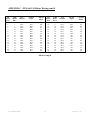
3.0 CONNECTING TO AN SA-11XX TARGET
3.1 General Information
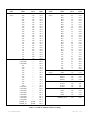
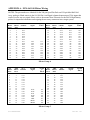
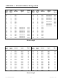
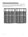
It is recommended that the user add Mictor connectors to their target for the interface to the
TLA600/700 using Tektronix P6434 high-density probes as we are unaware of a clip to permit
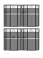
acquiring the signals directly from the micro. Table 1 shows the wiring and Channel Grouping
required for NEX-SA1100 support; Table 2 shows the same information but for NEX-SA1110 support.
IMPORTANT: Specific wiring must be followed when routing the microprocessor signals to Mictor
connectors if NEX-SA1100 or NEX-SA1110 support is going to be used. Appendix A “SA1100 to
Mictor Connector Wiring” shows the connections required for the SA1100; Appendix B “SA1110 to
Mictor Connector Wiring” shows the wiring required for the SA1110.
3.2 SA-1100 and GP26
The SA-1100 microprocessor does not offer, by default, a clock signal that can be used by a Logic
Analyzer to acquire bus information synchronously which makes disassembly support difficult if not
impossible. However, there is an option to use one of the General Purpose I/O pins, GP26, to provide a
clock that runs at ½ the core clock speed. The SA1100 and Brutus supports require that this clock
signal be enabled. Sample code to enable this signal and disable the internal data and instruction
caches, is provided in Appendix C “Sample Source Code”.
3.3 Intel Brutus Evaluation Board
The Intel Brutus evaluation board has Mictor connectors placed on it for easy access to the SA-1100
signals. However, in order for out Brutus support package to function properly several signals must be
moved by using a Nexus Technology NEX-HDSWIZ adapter for the C Group Mictor.
The HD-SWIZ must be modified as follows. The Target end of the HD-SWIZ is considered to be the
connector that plugs into the Mictor on the Brutus target. The TLA end of the HD-SWIZ is the
connector and latch housing, mounted on the larger PC board, that receives the P6434 probe from the
TLA:
Cut the PC board traces for Pins 3, 18, 19, and 36
Connect the following:
Target pin 7 to TLA pin 19
Target pin 9 to TLA pin 3
Target pin 11 to TLA pin 36
Target pin 6 to TLA pin 18
SA11XX-MN-XXX
6
Doc. Rev. 1.10
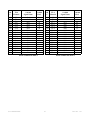
Then the TLA P6434s should be connected to the Brutus board as follows:
A Group Mictor to J11
E Group Mictor to J12
C Group Mictor to J13 (using the HD-SWIZ)
SA11XX-MN-XXX
7
Doc. Rev. 1.10
Group
Name
Address
(Hex)
DRAMAddr
Signal
Name
A25
A24
A23
A22
A21
A20
A19
A18
A17
A16
A15
A14
A13
A12
A11
A10
A9
A8
A7
A6
A5
A4
A3
A2
A1
A0
CASAddr10
CASAddr9
CASAddr8
A21
A20
A19
A18
A17
A16
A15
A14
A13
A12
A11
A10
CASAddr7
CASAddr6
CASAddr5
CASAddr4
CASAddr3
CASAddr2
CASAddr1
CASAddr0
DRAM_A1
DRAM_A0
SA1100
Pin #
137
138
139
140
143
144
145
146
147
148
149
150
155
156
157
158
159
160
163
164
165
166
167
168
169
170
----------------------------------------------ground
ground
TLA700
input
A3:1
A3:0
A2:7
A2:6
A2:5
A2:4
A2:3
A2:2
A2:1
A2:0
A1:7
A1:6
A1:5
A1:4
A1:3
A1:2
A1:1
A1:0
A0:7
A0:6
A0:5
A0:4
A0:3
A0:2
A0:1
A0:0
D2:4
D2:3
D2:2
A2:5
A2:4
A2:3
A2:2
A2:1
A2:0
A1:7
A1:6
A1:5
A1:4
A1:3
A1:2
D2:1
D2:0
D1:7
D1:6
D1:5
D1:4
D1:3
D1:2
D1:1
D1:0
Group
Name
Data
(Hex)
Control
(Sym)
RASlines
CASlines
Selects
Misc
Signal
Name
D31
D30
D29
D28
D27
D26
D25
D24
D23
D22
D21
D20
D19
D18
D17
D16
D15
D14
D13
D12
D11
D10
D9
D8
D7
D6
D5
D4
D3
D2
D1
D0
nOE
nWE
nRAS3
nRAS2
nRAS1
nRAS0
nCAS3
nCAS2
nCAS1
nCAS0
nCS3
nCS2
nCS1
nCS0
RCLK_OUT
nRESET_OUT
SA1100
Pin #
46
42
36
32
24
20
14
10
45
41
35
31
23
19
13
9
44
40
34
30
22
18
12
8
43
39
33
29
21
17
11
7
118
117
121
122
123
124
125
126
127
128
133
134
135
136
52
192
TLA700
input
E3:7
E3:6
E3:5
E3:4
E3:3
E3:2
E3:1
E3:0
E2:7
E2:6
E2:5
E2:4
E2:3
E2:2
E2:1
E2:0
E1:7
E1:6
E1:5
E1:4
E1:3
E1:2
E1:1
E1:0
E0:7
E0:6
E0:5
E0:4
E0:3
E0:2
E0:1
E0:0
C2:3
C2:2
CK3
CK2
C2:1
C2:0
Q3
Q2
Q1
Q0
C2:7
C2:6
C2:5
C2:4
CK1
CK0
Table 1- SA-1100 TLA600/700 Channel Grouping
SA11XX-MN-XXX
8
Doc. Rev. 1.10
Group
Name
Address
(Hex)
DRAMAddr
Signal
Name
A25
A24
A23
A22
A21
A20
A19
A18
A17
A16
A15
A14
A13
A12
A11
A10
A9
A8
A7
A6
A5
A4
A3
A2
A1
A0
A24
A23
A22
A21
A20
A19
A18
A17
A16
A15
A14
A13
A12
A11
A10
SA1110
BGA Pad #
F16
G13
F13
F15
E16
F14
E15
D16
E14
D15
C16
E13
D13
B16
C14
B14
B15
A16
A15
A14
B13
C13
A13
B12
C12
D12
G13
F13
F15
E16
F14
E15
D16
E14
D15
C16
E13
D13
B16
C14
B14
TLA700
input
A3:1
A3:0
A2:7
A2:6
A2:5
A2:4
A2:3
A2:2
A2:1
A2:0
A1:7
A1:6
A1:5
A1:4
A1:3
A1:2
A1:1
A1:0
A0:7
A0:6
A0:5
A0:4
A0:3
A0:2
A0:1
A0:0
A3:0
A2:7
A2:6
A2:5
A2:4
A2:3
A2:2
A2:1
A2:0
A1:7
A1:6
A1:5
A1:4
A1:3
A1:2
Group
Name
Data
(Hex)
Control
(Sym)
Misc
(Bin)
SDRAM_CS
(Bin)
Signal
Name
D31
D30
D29
D28
D27
D26
D25
D24
D23
D22
D21
D20
D19
D18
D17
D16
D15
D14
D13
D12
D11
D10
D9
D8
D7
D6
D5
D4
D3
D2
D1
D0
nSDRAS
nSDCAS
nOE
nWE
SDCLK0
nRESET_OUT
nSDCS3
nSDCS2
nSDCS1
nSDCS0
SA1110
BGA Pin #
M1
L2
K3
J3
H4
G3
F3
E3
M2
L3
K2
J2
G1
G4
E1
D1
L4
K4
J1
J6
H6
F1
E2
D2
L1
K1
J4
H1
G2
F2
F4
E4
M14
L16
M15
M13
P1
C7
TLA700
input
D3:7
D3:6
D3:5
D3:4
D3:3
D3:2
D3:1
D3:0
D2:7
D2:6
D2:5
D2:4
D2:3
D2:2
D2:1
D2:0
D1:7
D1:6
D1:5
D1:4
D1:3
D1:2
D1:1
D1:0
D0:7
D0:6
D0:5
D0:4
D0:3
D0:2
D0:1
D0:0
C2:0
C2:1
C2:3
C2:2
CK3
CK1
C3:3
C3:2
C3:1
C3:0
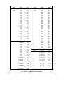
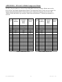
Table 2- SA-1110 TLA600/700 Channel Grouping
SA11XX-MN-XXX
9
Doc. Rev. 1.10
Group
Name
Address
(Hex)
DRAMAddr
Signal
Name
A25
A24
A23
A22
A21
A20
A19
A18
A17
A16
A15
A14
A13
A12
A11
A10
A9
A8
A7
A6
A5
A4
A3
A2
A1
A0
CASAddr9
CASAddr8
A19
A18
A17
A16
A15
A14
A13
A12
A11
A10
CASAddr7
CASAddr6
CASAddr5
CASAddr4
CASAddr3
CASAddr2
CASAddr1
CASAddr0
DRAM_A1
DRAM_A0
TLA600/700
input
A3:1
A3:0
A2:7
A2:6
A2:5
A2:4
A2:3
A2:2
A2:1
A2:0
A1:7
A1:6
A1:5
A1:4
A1:3
A1:2
A1:1
A1:0
A0:7
A0:6
A0:5
A0:4
A0:3
A0:2
A0:1
A0:0
D2:3
D2:2
A2:3
A2:2
A2:1
A2:0
A1:7
A1:6
A1:5
A1:4
A1:3
A1:2
D2:1
D2:0
D1:7
D1:6
D1:5
D1:4
D1:3
D1:2
D1:1
D1:0
Group
Name
Data
(Hex)
Control
(Sym)
RASlines
CASlines
Selects
Misc
Signal
Name
D31
D30
D29
D28
D27
D26
D25
D24
D23
D22
D21
D20
D19
D18
D17
D16
D15
D14
D13
D12
D11
D10
D9
D8
D7
D6
D5
D4
D3
D2
D1
D0
LA_OE#
LA_WE#
LA_RAS3#
LA_RAS2#
LA_RAS1#
LA_RAS0#
LA_CAS3#
LA_CAS2#
LA_CAS1#
LA_CAS0#
LA_CS3#
LA_CS2#
LA_CS1#
LA_CS0#
RCLK_OUT
TLA600/700
input
E3:7
E3:6
E3:5
E3:4
E3:3
E3:2
E3:1
E3:0
E2:7
E2:6
E2:5
E2:4
E2:3
E2:2
E2:1
E2:0
E1:7
E1:6
E1:5
E1:4
E1:3
E1:2
E1:1
E1:0
E0:7
E0:6
E0:5
E0:4
E0:3
E0:2
E0:1
E0:0
C2:3
C2:2
C3:7
C3:6
C2:1
C2:0
C3:3
CK3
C3:1
Q1
C2:7
C2:6
C2:5
C2:4
CK1
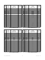
Table 3- Brutus TLA600/700 Channel Grouping
SA11XX-MN-XXX
10
Doc. Rev. 1.10
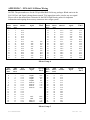
4.0 CONFIGURING THE SUPPORT
The SA-1100 microprocessor supports the use of DRAM for code execution memory. However,
because DRAM is accessed by Row and Column address cycles it becomes more difficult to translate
those two cycles into a physical address equivalent which is necessary for tracking the flow of program
code. The DRAMAddr group for Brutus support is already configured to properly reconstruct the
physical address from Row and Column information. The DRAMAddr group in the SA-1100 support
is configured by default for the largest memory configuration possible (16Mb). Some of the bits
presently in this group may need to be deleted to reflect a given target. Refer to Section 10.3 (Dynamic
Interface Operation) of the SA-1100 Microprocessor Technical Reference Manual for information on
how the DRAMAddr group should be configured for a specific target.
Note: During testing it appeared as if the complete proper physical address is placed on the Address
bus during the Row Address cycle. However, the SA-1100 documentation doesn’t appear to mention
this, and there was concern that this functionality may not be present in later versions of the micro, so
it was decided ignore this and instead create the DRAMAddr group to handle physical memory
addresses.
5.0 CLOCK SELECTION
5.1 SA-1100 and Brutus
5.1.1 General Information
There is one clocking option available when using the NEX-SA1100 and NEX-Brutus support
packages. The selections for this option are explained in detail below. As previously mentioned these
supports are designed to work with DRAM targets only. Please use the NEX-SA1110 support for
SDRAM targets.
The clocking mode is selected by moving to the System window, clicking on Setup for the appropriate
LA card, then clicking on More (a button to the right of the Clocking field). Choose the desired mode
in the Clocking Select field.
NOTE: Depending upon the speed of the SA-1100 micro and the design of the target it may be
necessary to adjust the Setup & Hold times for some of the NEX-SA1100 data groups to ensure proper
data acquisition. Please refer to Appendix C “Clocking Considerations” for further details.
5.1.2 Clocking Options - Explanation
Clocking Mode - Bus Cycle Clocking is the default clocking selection. In this mode the software
monitors the RCLK_OUT, nRAS0-3, and nCAS0-3 signals to permit the acquisition of SA-1100 bus
cycles only. All Wait and Idle states will be ignored, offering the best use of your acquisition memory.
Refer to Appendix B for more information on how bus cycle data is acquired. With Every Edge of
RCLK data will be acquired on every edge of the RCLK_OUT signal. The disassembly software will
try to filter and display these cycles accordingly, but incorrect decoding may occur because of the
SA11XX-MN-XXX
11
Doc. Rev. 1.10
numerous duplicated cycles. This clocking mode shows all bus cycles, including any Wait or idle
states. Since no clocking qualification is done only the RCLK signal is needed.
5.2 SA-1110
5.2.1 General Information
There are three clocking select fields available when using the NEX-SA1110 support package. Each is
explained in detail below. As previously mentioned the NEX-SA1110 support is designed to work with
SDRAM targets only. Please use the NEX-SA1100 support for DRAM targets.
The necessary clocking mode selections are made by moving to the System window, clicking on Setup
for the appropriate LA card, then clicking on More (a button to the right of the Clocking field). Choose
the desired mode in each Clocking Select field.
NOTE: Depending upon the speed of the SA-1110 micro and the design of the target it may be
necessary to adjust the Setup & Hold times for some of the NEX-SA1110 data groups to ensure proper
data acquisition. Please refer to Appendix C “Clocking Considerations” for further details.
5.2.2 Clocking Options - Explanation
Clocking Mode - This is set to Bus Cycle Clocking by default. In this mode the software monitors the
SDCLK0, nRAS, nCAS, and nWE signals to permit the acquisition of valid SA-1110 bus cycles only.
All Wait and Idle states will be ignored, offering the best use of your acquisition memory. Refer to
Appendix C for more information on how bus cycle data is acquired. Selecting Rising Edge of
SDCLK0 will acquire data on every rising edge of the SDCLK0 signal. The disassembly software will
try to filter and display these cycles accordingly, but incorrect decoding may occur because of the
numerous duplicated cycles. This clocking mode shows all bus cycles, including any Wait or idle
states. Since no clocking qualification is done only the SDCLK0 signal is needed.
CAS Latency – This field should be set to the proper value of the CAS latency for Read cycles. Valid
selections are 2 (default), 3, or 4 SDCLK cycles. Selecting the incorrect value will result in invalid
data acquisition during Read or Fetch cycles.
Read Burst Length – This field must be set to the length of Burst Read Cycles that the target is using.
Valid values are 1 (default), 4, or 8 cycles. The proper value must be set or improper Read and Fetch
data acquisition will result.
SA11XX-MN-XXX
12
Doc. Rev. 1.10
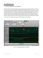
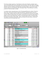
6.0 VIEWING DATA
6.1 Viewing Timing Data on the TLA600/700
By default, the TLA600/700 will display an acquisition in the Disassembly mode. However, the same
data can be displayed in Timing form by adding a Waveform Display window. This is done by clicking
on the Window pull-down, selecting New Data Window, clicking on Waveform Window Type, then
choosing the Data Source. Two choices are presented: SA1100 and SA1100-MagniVu. The first will
show the exact same data (same acquisition mode) as that shown in the Disassembly window, except
in Timing format. The second selection, SA1100-MagniVu, will show all of the channels in 2GHz
MagniVu mode, so that edge relationships can be examined at the module’s trigger point. With either
selection, all channels can be viewed by scrolling down the window. Refer to the TLA600/700 System
User’s Manual for additional information on formatting the Waveform display.
Figure 1- SA1100 MagniVu Display on TLA600/700
SA11XX-MN-XXX
13
Doc. Rev. 1.10
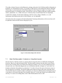
7.0 USING THE DISASSEMBLY SOFTWARE
7.1 General Information
The NEX-SA1100 support software acquires and decodes StrongARM SA-1100 bus activity and
displays the information as assembly language mnemonics (machine code) - see Figure 2. This permits
the tracing of code execution for debug purposes. It is possible to filter the data display cycle types of
interest to the software engineer (Figure 3). The user can choose to display the acquired data in
Hardware, Software, Control Flow, or Subroutine modes.
A major feature of the NEX-SA1100 software is its ability to intelligently acquire bus cycle
information. By taking advantage of the data clocking power built in to the Tektronix Logic Analyzers
the SA1100 software is able to acquire only the valid SA-1100 bus cycles and ignore Idle and Wait
states. This means that the user is able to make optimum use of the acquisition card’s memory and see
more microprocessor bus cycles. For debug purposes. the user also has the ability to override this
function and acquire data on every RCLK edge to permit the user to see all of the bus traffic including
the Idle and Wait states. (See Section 5.2 Clocking Options for further information.)
Every stored cycle (bus or clock edge, depending upon clocking selection) has a timestamp value
stored with it. This time information, accurate to 500ps in the TLA600/700 series, permits precise
measurements of microprocessor bus activity. Because of the design of Tektronix Logic Analyzers
there is no need to worry about trading off acquisition memory depth when making these
measurements, as the timestamp memory is separate from the acquisition memory.
7.2 Disassembly Using the TLA600/700
The TLA600/700, since it is a Windows program, has the same type of user interface as other
Windows-based applications. In the Disassembly Listing window, a tool bar at the top of the window
contains buttons that allow the user to modify the display. These buttons, from left to right, perform
the following functions:
Add Column - Adds a column to the display
Add Mark - Adds a user mark to the display
Cut - (may be grayed out) - Cuts the selection to the Clipboard
Copy - (may be grayed out) - Copies the selection to the Clipboard
Paste - (may be grayed out) - Inserts the contents of the Clipboard
Go To - Moves the display to the item of interest
Properties - Edits the current Listing Display properties
Smaller Font - Decreases the displayed font size
Larger Font - Increases the displayed font size
Search Backward - Moves to a previous data match
Define Search - Define data to be matched
Search Forward - Moves to the next data match
Mark Opcode - Permits placing an opcode mark
SA11XX-MN-XXX
14
Doc. Rev. 1.10
The format (or display properties) of each displayed column can be changed by putting the mouse
cursor on the heading of the column, clicking the left mouse button to select that column, clicking the
right mouse button to bring up the editing dialog, then selecting Properties. The column to be modified
can also be selected by clicking on the Column tab, selecting the column of interest in the Column
field, then making any desired modifications to that display column. The modification or selections
possible will vary from column to column.
Two display columns of particular interest are the Timestamp and Mnemonics columns. Timestamp
shows a time value associated with the acquisition. By default, Timestamp shows the time from
System Trigger. Clicking on the From window in the Timestamp Reference field shows all available
selections: Absolute (from when the Logic Analyzer was started), Previous (the time from the present
sequence to the previous displayed one), and three selections that permit time to be displayed from
different reference points: System Trigger, Cursor 1 Current Position, and Cursor 2 Current Position.
Selecting the desired mode with the mouse, and then clicking the left mouse button, will make the
selection the present Timestamp display mode.
Figure 2- SA1100 Disassembly
SA11XX-MN-XXX
15
Doc. Rev. 1.10
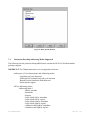
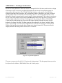
The other column of interest is the Mnemonics column, where the SA-1100 disassembly information is
displayed. As mentioned previously, it is possible to filter the SA-1100 instructions that are displayed.
This is done via selections made in the Disassembly tab of the Properties window (see Figure 3). By
default the display is in Hardware mode, where all bus cycles are displayed (Memory Reads, Memory
Writes, Instructions, etc.). Other choices are: Software (only executed instructions are displayed),
Control Flow (display of instructions affecting code flow such as Jumps, Branches, etc.), and
Subroutine (only instructions such as Calls, Returns, etc. are displayed).
Note that when data is suppressed in this fashion that Timestamp information (in Previous form) will
be updated to show the time between displayed cycles.
Figure 3- Disassembly Display Filter Window
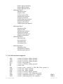
7.3
Help! The Disassembler’s Confused (or: Using Mark Opcode)
Because the SA-1100 does not have a signal to denote an opcode fetch, it is difficult to distinguish
between a Read cycle and an Opcode Fetch. The disassembly software does the best it can to figure
this out, but it assumes that every Read from contiguous memory cycles is a Fetch, and this may not
always be the case. When this happens the user can Mark an Opcode (a Sample or Cycle in the List
display) to help the disassembler re-synchronize. To do this, the user first moves the mouse cursor to
the cycle that is to be marked. Click on the right mouse button to bring up the menu selections, then
click on Mark Opcode. Another window will appear (see Figure 4) which permits selecting the type of
cycle that is to be marked (Opcode Fetch, Memory Read, etc.). Select the desired cycle and then click
on Okay. To remove an existing Mark, select Undo Mark and then click on OK.
SA11XX-MN-XXX
16
Doc. Rev. 1.10
Figure 4- Mark Opcode Window
7.4
Instruction Decoding/Addressing Modes Supported
The following lists the particular StrongARM feature sets that the NEX-SA1100 disassembler
packages supports.
IMPORTANT: The Thumb instruction set is not supported at this time.
Architecture v4 Level Instructions and Addressing modes
- Load data read cycle detection
- LDM and LDC multiple load read cycle detection
- Branch Prefetch Instruction flush detection
- Mark-Opcode support
All five addressing modes:
Addressing Mode 1
- Shifter operands
- Immediate
- Register
- Logical shift left by immediate
- Logical shift left by register
- Logical shift right by immediate
- Logical shift right by register
- Arithmetic shift right by immediate
- Arithmetic shift right by register
SA11XX-MN-XXX
17
Doc. Rev. 1.10
- Rotate right by immediate
- Rotate right by register
- Rotate right with extend
Addressing Mode 2
- Immediate offset
- Register offset
- Scaled register offset
- Immediate pre-indexed
- Register pre-indexed
- Scaled register pre-indexed
- Immediate post-indexed
- Register post-indexed
- Scaled register post-indexed
Addressing Mode 3
- Immediate offset
- Register offset
- Immediate pre-indexed
- Register pre-indexed
- Immediate post-indexed
- Register post-indexed
Addressing Mode 4
- Increment after
- Increment before
- Decrement after
- Decrement before
Addressing Mode 5
- Immediate offset
- Immediate pre-indexed
- Immediate post-indexed
7.5 SA-1100 Instructions Supported
ADC
ADD
AND
B{L}
BIC
BX
CDP
CMN
CMP
EOR
LDC
LDM
LDM
SA11XX-MN-XXX
{<cond>}{S} Rd, Rn, <shifter_operand>
{<cond>}{S} Rd, Rn, <shifter_operand>
{<cond>}{S} Rd, Rn, <shifter_operand>
{<cond>} <target address>
{<cond>}{S} Rd, Rn, <shifter_operand>
{<cond>} Rm
{<cond>} p<cp#>, <opcode_1>, CRd, CRn, CRm, <opcode_2>
{<cond>} Rn, <shifter_operand>
{<cond>} Rn, <shifter_operand>
{<cond>}{S} Rd, Rn, <shifter_operand>
{<cond>} p<cp_num>, CRd, <addressing_mode>
{<cond>} <addressing_mode> Rn{!}, <registers>
{<cond>} <addressing_mode> Rn, <registers>^
18
LDM(1)
LDM(2)
Doc. Rev. 1.10
LDM
LDM(3)
LDR
LDR
LDR
LDR
LDR
LDR
LDR
MCR
MLA
MOV
MRC
MRS
MRS
MSR
MSR
MSR
MSR
MUL
MVN
ORR
RSB
RSC
SBC
SMLAL
SMULL
STC
STM
STM
STR
STR
STR
STR
STR
SUB
SWI
SWP
SWP
TEQ
TST
UMLAL
UMULL
SA11XX-MN-XXX
{<cond>} <addressing_mode> Rn{!}, <registers_and_pc>^
{<cond>} Rd, <addressing_mode>
{<cond>}B Rd, <addressing_mode>
{<cond>}BT Rd, <post_indexed_addressing_mode>
{<cond>}H Rd, <addressing_mode>
{<cond>}SB Rd, <addressing_mode>
{<cond>}SH Rd, <addressing_mode>
{<cond>}T Rd, <post_indexed_addressing_mode>
{<cond>} p<cp#>, <opcode_1>, Rd, CRn, CRm, <opcode_2>
{<cond>}{<S>} Rd, Rm, Rs, Rn
{<cond>}{S} Rd, <shifter_operand>
{<cond>} p<cp#>, <opcode_1>, Rd, CRn, CRm, <opcode_2>
{<cond>} Rd, CPSR
{<cond>} Rd, SPSR
{<cond>} Rd, CPSR_f, #32bit immediate
{<cond>} Rd, CPSR_<fields>, Rm
{<cond>} Rd, SPSR_f, #32bit immediate
{<cond>} Rd, SPSR_<fields>, Rm
{<cond>}{<S>}Rd, Rm, Rs
{<cond>}{<S>} Rd, <shifter_operand>
{<cond>}{S} Rd, Rn, <shifter_operand>
{<cond>}{S} Rd, Rn, <shifter_operand>
{<cond>}{S} Rd, Rn, <shifter_operand>
{<cond>}{S} Rd, Rn, <shifter_operand>
{<cond>}{<S>} RdLo, RdHi, Rm, Rs
{<cond>}{<S>} RdLo, RdHi, Rm, Rs
{<cond>} p<cp_num>, CRd, <addressing_mode>
{<cond>} <addressing_mode> Rn{!}, <registers>
{<cond>} <addressing_mode> Rn{!}, <registers>^
{<cond>} Rd, <addressing_mode>
{<cond>}B Rd, <addressing_mode>
{<cond>}BT Rd, <post_indexed_addressing_mode>
{<cond>}H Rd, <addressing_mode>
{<cond>}T Rd, <post_indexed_addressing_mode>
{<cond>}{<S>} Rd, Rn, <shifter_operand>
{<cond>} <24_bit_immediate>
{<cond>} Rd, Rm, [Rn]
{<cond>}B Rd, Rm, [Rn]
{<cond>} Rn, <shifter_operand>
{<cond>} Rn, <shifter_operand>
{<cond>}{<S>} RdLo, RdHi, Rm, Rs
{<cond>}{<S>} RdLo, RdHi, Rm, Rs
19
STM(1)
STM(2)
Doc. Rev. 1.10
8.0 CONTROL GROUP SYMBOL TABLES
The use of Symbol Tables when displaying state data and defining a trigger enables the user to quickly
determine the type of bus cycle that occurred or is desired. Symbol tables for the Control group
(SA1100_Ctrl / NEX-Brutus Table 4 and SA1110_Ctrl Table 5) have been provided to quickly show
the type of bus transaction acquired when viewing data in Listing display. This same symbol table can
be used in the Trigger area of the TLA to easily define the sort of bus cycle that is to be triggered on.
Pattern
01
10
TLA600/700 Symbols
READ/FETCH
WRITE
Meaning
Read or Fetch Cycle
Write Cycle
Table 4- NEX-SA1100 / NEX-Brutus Control Symbol Table
Signals, from left to right: nOE, nWE
Pattern
1xx1
1xx0
01xx
10xx
00xx
TLA600/700 Symbols
READ/FETCH
WRITE
RAS_CYCLE
CAS_CYCLE
REFRESH
Meaning
Read or Fetch Cycle
Write Cycle
RAS Address Cycle
CAS Address Cycle
Memory Refresh Cycle
Table 5- NEX-SA1110 Control Symbol Table
Signals, from left to right: nSDRAS, nSDCAS, nOE, nWE
SA11XX-MN-XXX
20
Doc. Rev. 1.10
APPENDIX A - NEX-SA1100 Mictor Wiring
NOTES: The pin numbers are identical for the 208-pin Quad Flat Pack and 256-pin Mini-Ball Grid
Array packages. Blank entries in the SA1100 Pin # and Signal columns denote unused TLA inputs that
can be wired to any user signal. Please refer to the manual from Tektronix for the P6434 High Density
probes for important information on designing the necessary connectors into a target system.
Tek
Mictor
Pin #
3
4
5
6
7
8
9
10
11
12
13
14
15
16
17
18
19
AMP
Mictor
Pin #
5
7
9
11
13
15
17
19
21
23
25
27
29
31
33
35
37
TLA
Channel
SA1100
Signal
SA1100
CK0
A3:7
A3:6
A3:5
A3:4
A3:3
A3:2
A3:1
A3:0
A2:7
A2:6
A2:5
A2:4
A2:3
A2:2
A2:1
A2:0
nRESET_OUT
192
A25
A24
A23
A22
A21
A20
A19
A18
A17
A16
137
138
139
140
143
144
145
146
147
148
Tek
Mictor
Pin #
36
35
34
33
32
31
30
29
28
27
26
25
24
23
22
21
20
Pin #
AMP
Mictor
Pin #
6
8
10
12
14
16
18
20
22
24
26
28
30
32
34
36
38
TLA
Channe
l
CK1
A1:7
A1:6
A1:5
A1:4
A1:3
A1:2
A1:1
A1:0
A0:7
A0:6
A0:5
A0:4
A0:3
A0:2
A0:1
A0:0
AMP
Mictor
Pin #
6
8
10
12
14
16
18
20
22
24
26
28
30
32
34
36
38
TLA
Channel
SA1100
Signal
SA1100
Q1
C1:7
C1:6
C1:5
C1:4
C1:3
C1:2
C1:1
C1:0
C0:7
C0:6
C0:5
C0:4
C0:3
C0:2
C0:1
C0:0
nCAS1
127
SA1100
Signal
SA1100
GP26
A15
A14
A13
A12
A11
A10
A9
A8
A7
A6
A5
A4
A3
A2
A1
A0
52
149
150
155
156
157
158
159
160
163
164
165
166
167
168
169
170
Pin #
Mictor Group A
Tek
Mictor
Pin #
3
4
5
6
7
8
9
10
11
12
13
14
15
16
17
18
19
AMP
Mictor
Pin #
5
7
9
11
13
15
17
19
21
23
25
27
29
31
33
35
37
TLA
Channel
SA1100
Signal
Tek
Mictor
Pin #
36
35
34
33
32
31
30
29
28
27
26
25
24
23
22
21
20
SA110
0
Pin #
CK3
C3:7
C3:6
C3:5
C3:4
C3:3
C3:2
C3:1
C3:0
C2:7
C2:6
C2:5
C2:4
C2:3
C2:2
C2:1
C2:0
nRAS3
121
nCS3
nCS2
nCS1
nCS0
nOE
nWE
nRAS1
nRAS0
133
134
135
136
118
117
123
124
Pin #
Mictor Group C
SA11XX-MN-XXX
21
Doc. Rev. 1.10
APPENDIX A - NEX-SA1100 Mictor Wiring (cont’d)
Tek
Mictor
Pin #
3
4
5
6
7
8
9
10
11
12
13
14
15
16
17
18
19
AMP
Mictor
Pin #
5
7
9
11
13
15
17
19
21
23
25
27
29
31
33
35
37
TLA
Channel
SA1100
Signal
SA1100
Q0
D3:7
D3:6
D3:5
D3:4
D3:3
D3:2
D3:1
D3:0
D2:7
D2:6
D2:5
D2:4
D2:3
D2:2
D2:1
D2:0
nCAS0
128
Do Not
Do Not
Do Not
Do Not
Do Not
Do Not
Do Not
Do Not
Use
Use
Use
Use
Use
Use
Use
Use
Tek
Mictor
Pin #
36
35
34
33
32
31
30
29
28
27
26
25
24
23
22
21
20
Pin #
DNU
DNU
DNU
DNU
DNU
DNU
DNU
DNU
AMP
Mictor
Pin #
6
8
10
12
14
16
18
20
22
24
26
28
30
32
34
36
38
TLA
Channel
SA1100
Signal
SA1100
CK2
D1:7
D1:6
D1:5
D1:4
D1:3
D1:2
D1:1
D1:0
D0:7
D0:6
D0:5
D0:4
D0:3
D0:2
D0:1
D0:0
nRAS2
Do Not Use
Do Not Use
Do Not Use
Do Not Use
Do Not Use
Do Not Use
Do Not Use
Do Not Use
122
DNU
DNU
DNU
DNU
DNU
DNU
DNU
DNU
AMP
Mictor
Pin #
6
8
10
12
14
16
18
20
22
24
26
28
30
32
34
36
38
TLA
Channel
SA1100
Signal
SA1100
Q2
E1:7
E1:6
E1:5
E1:4
E1:3
E1:2
E1:1
E1:0
E0:7
E0:6
E0:5
E0:4
E0:3
E0:2
E0:1
E0:0
nCAS2
D15
D14
D13
D12
D11
D10
D9
D8
D7
D6
D5
D4
D3
D2
D1
D0
126
44
40
34
30
22
18
12
8
43
39
33
29
21
17
11
7
Pin #
Mictor Group D
Tek
Mictor
Pin #
3
4
5
6
7
8
9
10
11
12
13
14
15
16
17
18
19
AMP
Mictor
Pin #
5
7
9
11
13
15
17
19
21
23
25
27
29
31
33
35
37
TLA
Channel
SA1100
Signal
SA1100
Q3
E3:7
E3:6
E3:5
E3:4
E3:3
E3:2
E3:1
E3:0
E2:7
E2:6
E2:5
E2:4
E2:3
E2:2
E2:1
E2:0
nCAS3
D31
D30
D29
D28
D27
D26
D25
D24
D23
D22
D21
D20
D19
D18
D17
D16
125
46
42
36
32
24
20
14
10
45
41
35
31
23
19
13
9
Tek
Mictor
Pin #
36
35
34
33
32
31
30
29
28
27
26
25
24
23
22
21
20
Pin #
Pin #
Mictor Group E
SA11XX-MN-XXX
22
Doc. Rev. 1.10
APPENDIX B - NEX-SA1100 P6860 Compression Pinout
NOTES: The pin numbers are identical for the 208-pin Quad Flat Pack and 256-pin Mini-Ball Grid
Array packages. Blank entries in the SA1100 Pin # and Signal columns denote unused TLA inputs that
can be wired to any user signal. For further information on the P6860 Connectorless probe
compression footprint, please refer to the “P6810, P6860 and P6880 Logic Analyzer Probes Instruction
Manual”, Tektronix part number 071-1059-00.
Pad
#
TLA
Channel
SA1100
Signal
Name
SA1100
Pin #
Pad
#
TLA
Channel
SA1100
Signal
Name
SA1100
Pin #
A15
A13
B12
B10
A12
A10
B9
B7
A9
A7
B6
B4
A6
A4
B3
B1
A3
A1
CK1CK1+
A1:7
A1:6
A1:5
A1:4
A1:3
A1:2
A1:1
A1:0
A0:7
A0:6
A0:5
A0:4
A0:3
A0:2
A0:1
A0:0
Gnd
GP26
A15
A14
A13
A12
A11
A10
A9
A8
A7
A6
A5
A4
A3
A2
A1
A0
Gnd
52
149
150
155
156
157
158
159
160
163
164
165
166
167
168
169
170
A15
A13
B12
B10
A12
A10
B9
B7
A9
A7
B6
B4
A6
A4
B3
B1
A3
A1
CK0CK0+
A3:7
A3:6
A3:5
A3:4
A3:3
A3:2
A3:1
A3:0
A2:7
A2:6
A2:5
A2:4
A2:3
A2:2
A2:1
A2:0
Gnd
nRESET_OUT
Gnd
192
A25
A24
A23
A22
A21
A20
A19
A18
A17
A16
137
138
139
140
143
144
145
146
147
148
Probe Connection A0/A1
SA11XX-MN-XXX
Probe Connection A2/A3
23
Doc. Rev. 1.10
Pad
#
TLA
Channel
SA1100
Signal Name
SA1100
Pin #
Pad
#
TLA
Channel
SA1100
Signal Name
SA1100
Pin #
A15
A13
B12
B10
A12
A10
B9
B7
A9
A7
B6
B4
A6
A4
B3
B1
A3
A1
Q1Q1+
C1:7
C1:6
C1:5
C1:4
C1:3
C1:2
C1:1
C1:0
C0:7
C0:6
C0:5
C0:4
C0:3
C0:2
C0:1
C0:0
Gnd
nCAS1
Gnd
127
A15
A13
B12
B10
A12
A10
B9
B7
A9
A7
B6
B4
A6
A4
B3
B1
A3
A1
CK3CK3+
C3:7
C3:6
C3:5
C3:4
C3:3
C3:2
C3:1
C3:0
C2:7
C2:6
C2:5
C2:4
C2:3
C2:2
C2:1
C2:0
Gnd
nRAS3
Gnd
121
nCS3
nCS2
nCS1
nCS0
nOE
nWE
nRAS1
nRAS0
133
134
135
136
118
117
123
124
Probe Connection C0/C1
Probe Connection C2/C3
Pad
#
TLA
Channel
SA1100
Signal Name
SA1100
Pin #
Pad
#
TLA
Channel
SA1100
Signal Name
SA1100
Pin #
A15
A13
B12
B10
A12
A10
B9
B7
A9
A7
B6
B4
A6
A4
B3
B1
A3
A1
CK2CK2+
D1:7
D1:6
D1:5
D1:4
D1:3
D1:2
D1:1
D1:0
D0:7
D0:6
D0:5
D0:4
D0:3
D0:2
D0:1
D0:0
Gnd
nRAS2
Do Not Use
Do Not Use
Do Not Use
Do Not Use
Do Not Use
Do Not Use
Do Not Use
Do Not Use
Gnd
122
DNU
DNU
DNU
DNU
DNU
DNU
DNU
DNU
A15
A13
B12
B10
A12
A10
B9
B7
A9
A7
B6
B4
A6
A4
B3
B1
A3
A1
Q0Q0+
D3:7
D3:6
D3:5
D3:4
D3:3
D3:2
D3:1
D3:0
D2:7
D2:6
D2:5
D2:4
D2:3
D2:2
D2:1
D2:0
Gnd
nCAS0
Gnd
128
Do Not Use
Do Not Use
Do Not Use
Do Not Use
Do Not Use
Do Not Use
Do Not Use
Do Not Use
DNU
DNU
DNU
DNU
DNU
DNU
DNU
DNU
Probe Connection D0/D1
SA11XX-MN-XXX
Probe Connection D2/D3
24
Doc. Rev. 1.10
Pad
#
TLA
Channel
SA1100
Signal Name
SA1100
Pin #
Pad
#
TLA
Channel
SA1100
Signal Name
SA1100
Pin #
A15
A13
B12
B10
A12
A10
B9
B7
A9
A7
B6
B4
A6
A4
B3
B1
A3
A1
Q2Q2+
E1:7
E1:6
E1:5
E1:4
E1:3
E1:2
E1:1
E1:0
E0:7
E0:6
E0:5
E0:4
E0:3
E0:2
E0:1
E0:0
Gnd
nCAS2
D15
D14
D13
D12
D11
D10
D9
D8
D7
D6
D5
D4
D3
D2
D1
D0
Gnd
126
44
40
34
30
22
18
12
8
43
39
33
29
21
17
11
7
A15
A13
B12
B10
A12
A10
B9
B7
A9
A7
B6
B4
A6
A4
B3
B1
A3
A1
Q3Q3+
E3:7
E3:6
E3:5
E3:4
E3:3
E3:2
E3:1
E3:0
E2:7
E2:6
E2:5
E2:4
E2:3
E2:2
E2:1
E2:0
Gnd
nCAS3
D31
D30
D29
D28
D27
D26
D25
D24
D23
D22
D21
D20
D19
D18
D17
D16
Gnd
125
46
42
36
32
24
20
14
10
45
41
35
31
23
19
13
9
Probe Connection E0/E1
SA11XX-MN-XXX
Probe Connection E2/E3
25
Doc. Rev. 1.10
APPENDIX C - NEX-SA1110 Mictor Wiring
NOTES: The pin numbers are for the 256-pin Mini-Ball Grid Array packages. Blank entries in the
SA1110 Pin # and Signal columns denote unused TLA inputs that can be wired to any user signal.
Please refer to the manual from Tektronix for the P6434 High Density probes for important
information on designing the necessary connectors into a target system.
Tek
Mictor
Pin #
3
4
5
6
7
8
9
10
11
12
13
14
15
16
17
18
19
AMP
Mictor
Pin #
5
7
9
11
13
15
17
19
21
23
25
27
29
31
33
35
37
TLA
Channel
CK0
A3:7
A3:6
A3:5
A3:4
A3:3
A3:2
A3:1
A3:0
A2:7
A2:6
A2:5
A2:4
A2:3
A2:2
A2:1
A2:0
SA1110
Signal
A25
A24
A23
A22
A21
A20
A19
A18
A17
A16
SA1110
Pin #
F16
G13
F13
F15
E16
F14
E15
D16
E14
D15
Tek
Mictor
Pin #
36
35
34
33
32
31
30
29
28
27
26
25
24
23
22
21
20
AMP
Mictor
Pin #
6
8
10
12
14
16
18
20
22
24
26
28
30
32
34
36
38
TLA
Channel
SA1110
Signal
SA1110
CK1
A1:7
A1:6
A1:5
A1:4
A1:3
A1:2
A1:1
A1:0
A0:7
A0:6
A0:5
A0:4
A0:3
A0:2
A0:1
A0:0
nRESET_OUT
A15
A14
A13
A12
A11
A10
A9
A8
A7
A6
A5
A4
A3
A2
A1
A0
C7
C16
E13
D13
B16
C14
B14
B15
A16
A15
A14
B13
C13
A13
B12
C12
D12
AMP
Mictor
Pin #
6
8
10
12
14
16
18
20
22
24
26
28
30
32
34
36
38
TLA
Channel
SA1110
Signal
SA1110
Pin #
Mictor Group A
Tek
Mictor
Pin #
3
4
5
6
7
8
9
10
11
12
13
14
15
16
17
18
19
AMP
Mictor
Pin #
5
7
9
11
13
15
17
19
21
23
25
27
29
31
33
35
37
TLA
Channel
SA1110
Signal
SA1110
CK3
C3:7
C3:6
C3:5
C3:4
C3:3
C3:2
C3:1
C3:0
C2:7
C2:6
C2:5
C2:4
C2:3
C2:2
C2:1
C2:0
SDCLK0
DQM3
DQM2
DQM1
DQM0
nSDCS3
nSDCS2
nSDCS1
nSDCS0
P1
K13
K15
J15
J14
L15
L14
L13
K16
nOE
nWE
nSDCAS
nSDRAS
M15
M13
L16
M14
Pin #
Tek
Mictor
Pin #
36
35
34
33
32
31
30
29
28
27
26
25
24
23
22
21
20
Pin #
Q1
C1:7
C1:6
C1:5
C1:4
C1:3
C1:2
C1:1
C1:0
C0:7
C0:6
C0:5
C0:4
C0:3
C0:2
C0:1
C0:0
Mictor Group C
SA11XX-MN-XXX
26
Doc. Rev. 1.10
APPENDIX C - NEX-SA1110 Mictor Wiring (cont’d)
Tek
Mictor
Pin #
3
4
5
6
7
8
9
10
11
12
13
14
15
16
17
18
19
AMP
Mictor
Pin #
5
7
9
11
13
15
17
19
21
23
25
27
29
31
33
35
37
TLA
Channel
SA1110
Signal
SA1110
Q0
D3:7
D3:6
D3:5
D3:4
D3:3
D3:2
D3:1
D3:0
D2:7
D2:6
D2:5
D2:4
D2:3
D2:2
D2:1
D2:0
D31
D30
D29
D28
D27
D26
D25
D24
D23
D22
D21
D20
D19
D18
D17
D16
M1
L2
K3
J3
H4
G3
F3
E3
M2
L3
K2
J2
G1
G4
E1
D1
Tek
Mictor
Pin #
36
35
34
33
32
31
30
29
28
27
26
25
24
23
22
21
20
Pin #
AMP
Mictor
Pin #
6
8
10
12
14
16
18
20
22
24
26
28
30
32
34
36
38
TLA
Channel
SA1110
Signal
SA1110
CK2
D1:7
D1:6
D1:5
D1:4
D1:3
D1:2
D1:1
D1:0
D0:7
D0:6
D0:5
D0:4
D0:3
D0:2
D0:1
D0:0
D15
D14
D13
D12
D11
D10
D9
D8
D7
D6
D5
D4
D3
D2
D1
D0
L4
K4
J1
J6
H6
F1
E2
D2
L1
K1
J4
H1
G2
F2
F4
E4
Pin #
Mictor Group D
SA11XX-MN-XXX
27
Doc. Rev. 1.10
APPENDIX D - NEX-SA1110 P6860 Compression Pinout
NOTES: The pin numbers are for the 256-pin Mini-Ball Grid Array packages. Blank entries in the
SA1110 Pin # and Signal columns denote unused TLA inputs that can be wired to any user signal. For
further information on the P6860 Connectorless probe compression footprint, please refer to the
“P6810, P6860 and P6880 Logic Analyzer Probes Instruction Manual”, Tektronix part number 0711059-00.
Pad
#
TLA
Channel
SA1110
Signal
Name
SA1110
Pin #
Pad
#
TLA
Channel
SA1110
Signal
Name
SA1110
Pin #
A15
A13
B12
B10
A12
A10
B9
B7
A9
A7
B6
B4
A6
A4
B3
B1
A3
A1
CK1CK1+
A1:7
A1:6
A1:5
A1:4
A1:3
A1:2
A1:1
A1:0
A0:7
A0:6
A0:5
A0:4
A0:3
A0:2
A0:1
A0:0
Gnd
nRESET_OUT
A15
A14
A13
A12
A11
A10
A9
A8
A7
A6
A5
A4
A3
A2
A1
A0
Gnd
C7
C16
E13
D13
B16
C14
B14
B15
A16
A15
A14
B13
C13
A13
B12
C12
D12
A15
A13
B12
B10
A12
A10
B9
B7
A9
A7
B6
B4
A6
A4
B3
B1
A3
A1
CK0CK0+
A3:7
A3:6
A3:5
A3:4
A3:3
A3:2
A3:1
A3:0
A2:7
A2:6
A2:5
A2:4
A2:3
A2:2
A2:1
A2:0
Gnd
Gnd
A25
A24
A23
A22
A21
A20
A19
A18
A17
A16
F16
G13
F13
F15
E16
F14
E15
D16
E14
D15
Probe Connection A0/A1
SA11XX-MN-XXX
Probe Connection A2/A3
28
Doc. Rev. 1.10
Pad
#
TLA
Channel
SA1110
Signal Name
SA1110
Pin #
Pad
#
TLA
Channel
SA1110
Signal Name
SA1110
Pin #
A15
A13
B12
B10
A12
A10
B9
B7
A9
A7
B6
B4
A6
A4
B3
B1
A3
A1
Q1Q1+
C1:7
C1:6
C1:5
C1:4
C1:3
C1:2
C1:1
C1:0
C0:7
C0:6
C0:5
C0:4
C0:3
C0:2
C0:1
C0:0
Gnd
Gnd
A15
A13
B12
B10
A12
A10
B9
B7
A9
A7
B6
B4
A6
A4
B3
B1
A3
A1
CK3CK3+
C3:7
C3:6
C3:5
C3:4
C3:3
C3:2
C3:1
C3:0
C2:7
C2:6
C2:5
C2:4
C2:3
C2:2
C2:1
C2:0
Gnd
SDCLK0
DQM3
DQM2
DQM1
DQM0
nSDCS3
nSDCS2
nSDCS1
nSDCS0
Gnd
P1
K13
K15
J15
J14
L15
L14
L13
K16
nOE
nWE
nSDCAS
nSDRAS
M15
M13
L16
M14
Probe Connection C0/C1
Probe Connection C2/C3
Pad
#
TLA
Channel
SA1110
Signal Name
SA1110
Pin #
Pad
#
TLA
Channel
SA1110
Signal Name
SA1110
Pin #
A15
A13
B12
B10
A12
A10
B9
B7
A9
A7
B6
B4
A6
A4
B3
B1
A3
A1
CK2CK2+
D1:7
D1:6
D1:5
D1:4
D1:3
D1:2
D1:1
D1:0
D0:7
D0:6
D0:5
D0:4
D0:3
D0:2
D0:1
D0:0
Gnd
Gnd
Gnd
L4
K4
J1
J6
H6
F1
E2
D2
L1
K1
J4
H1
G2
F2
F4
E4
Q0Q0+
D3:7
D3:6
D3:5
D3:4
D3:3
D3:2
D3:1
D3:0
D2:7
D2:6
D2:5
D2:4
D2:3
D2:2
D2:1
D2:0
Gnd
D15
D14
D13
D12
D11
D10
D9
D8
D7
D6
D5
D4
D3
D2
D1
D0
A15
A13
B12
B10
A12
A10
B9
B7
A9
A7
B6
B4
A6
A4
B3
B1
A3
A1
D31
D30
D29
D28
D27
D26
D25
D24
D23
D22
D21
D20
D19
D18
D17
D16
M1
L2
K3
J3
H4
G3
F3
E3
M2
L3
K2
J2
G1
G4
E1
D1
Probe Connection D0/D1
SA11XX-MN-XXX
Probe Connection D2/D3
29
Doc. Rev. 1.10
APPENDIX E - Necessary Signals for Clocking
To properly acquire SA-1100 bus activity in Bus Cycle Clocking mode (see Section 5.0 for further
information on this mode), the following signals must be provided: RCLK_OUT, nRAS0-3, and
nCAS0-3. If Bus Cycle Clocking does not work, move to the Activity Indicator window of the TLA
and observe that all of these signals are toggling.
When using the NEX-SA1100 support in Every Edge of RCLK mode, the only signal that is required
is RCLK_OUT, and this signal must show activity in the Activity Indicator window of the TLA.
SA11XX-MN-XXX
30
Doc. Rev. 1.10
APPENDIX F - SAMPLE SOURCE CODE
As previously mentioned it is necessary to define the GP26 signal as an external clock source for micro
data to be acquired synchronously by the Logic Analyzer. It is also strongly recommended that both
the instruction and data caches be disabled to permit the Analyzer to better track the flow of the
codeand we have provided some examples to do this. The code is available on the TLA’s hard disk in
one of the following folders (depending upon which support was loaded:
C:\Program Files\TLA 700\Supports\Brutus
C:\Program Files\TLA 700\Supports\SA1100
with the filename NewWaveInit.s . The code is also listed below:
; turns on external rclk
; disables both icache and dcache
;
GPIODirect EQU 0x90040004
GPIOAltFunc EQU 0x9004001c
RclkMask EQU 0x04000000
TUCRegister EQU 0x90030008
Bit31Mask EQU 0x80000000
EnableDcache
EnableWB
EnableIcache
EQU 0x4
EQU 0x8
EQU 0x1000
FlushCacheOPC2 EQU 0x0
FlushCacheCRm EQU 0x7
SWI_Angel
EQU 0x123456
angel_SWIreason_EnterSVC EQU 0x17
AREA |Random$$code|, CODE, READONLY
EXPORT NewWaveInit
NewWaveInit
STMFD sp!, {v1-v3, lr} ; save working registers
MOV v3, sp
; save stack pointer...
; must enter supervisor mode to disable caches
SA11XX-MN-XXX
31
Doc. Rev. 1.10
MOV r0, #angel_SWIreason_EnterSVC ; Enter SVC mode
SWI SWI_Angel
; Returns EnterUSR routine in r0
MRC p15, 0, r4, c1, c0 ,0 ; read the control register
BIC r4, r4, #EnableIcache ; turn off Icache
BIC r4, r4, #EnableDcache ; turn off Dcache
BIC r4, r4, #EnableWB
MCR p15, 0, r4, c1, c0 ,0 ; write the control register
; now back to user mode
MOV sp, v3
; restore stack pointer
LDMFD sp!, {v1-v3, lr} ; restore registers
; now we must flush the icache, we flush both
; because nothing of significance to the user has
; happened so far, we want all data reads to show up
; and we just restored all the registers from the stack
; (which may have been cached)
MOV r4, #0
MCR p15, 0, r4, c7, c7, 0
LDR r0, =GPIODirect ; GPDR - GPIO Direction Register
LDR r1, =GPIOAltFunc ; GAFR - GPIO Alternate Function Register
LDR r2, =RclkMask ; GPIO26 (rclk) Mask Bit
; We must set GPIO Direction and GPIO Alternate Function Registers
; Bit 26 on to enable RCLK_OUT
LDR r3, [r0] ; Get current GPDR contents
LDR r4, [r1] ; Get current GAFR contents
ORR r5, r3, r2 ; Set Bit 26 true (1)
STR r5, [r0] ; Write GPDR to set Bit 26 as an Output
ORR r5, r4, r2 ; Set Bit 26 true (1)
STR r5, [r1] ; Write GAFR Bit 26 for RCLK_OUT
; We must also set Bit 31 of TUCR to output clock
LDR r0, =TUCRegister ; TUCR - Test Control Register
LDR r1, =Bit31Mask ; Bit 31 Mask
LDR r3, [r0] ; Get current TUCR contents
ORR r5, r3, r1 ; Set Bit 31 true (1)
STR r5, [r0] ; Write TUCR to set Bit 31
END
SA11XX-MN-XXX
32
Doc. Rev. 1.10
APPENDIX G - Clocking Considerations
Because of timing differences between versions of StrongARM SA-1100 micro, and also due to design
of the target, it may be necessary to adjust the sample point of some of the acquisition groups for
ensure proper data acquisition. The TLA600/700 Logic Analyzer cards require a 2ns stable data
window to guarantee data acquisition, and by default this window is defined as 2ns Setup / 0ns Hold
(for all groups) relative to the RCLK_OUT clock edge. However, this Setup and Hold value can be
adjusted on a group-by-group basis to meet the target’s timing requirements. This is done by moving to
the LA card’s Setup window and clicking on the More button next to the right of the Clocking field. A
window similar to that shown in Figure 4 will appear. In this example the Address, DRAMAddr,
Control and RASAddr groups have been left at the Support Package Defaults selection, which is
defined as 2ns Setup / 0ns Hold. The Data group has been adjusted to 1ns Setup / 1ns Hold. When
using a TLA running V3.0 software these adjustments are made by left-clicking on the Setup/Hold
Window field and then choosing the desired Setup value from the menu field. The process may be
slightly different when using earlier versions of TLA software.
Figure 5- Setup & Hold Adjustment
The same concerns exist for the SA-1110 micro and designs using it. The data groups that may need to
be adjusted are the Address, DRAMAddr, Data, and Control groups.
SA11XX-MN-XXX
33
Doc. Rev. 1.10
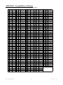
APPENDIX H - StrongARM SA-1100 Pinout
This table shows the pinouts for the 208-pin Quad Flat Pack and 256-pin mini-BGA packages:
QFP
Pin #
1
2
3
4
5
6
7
8
9
10
11
12
13
14
15
16
17
18
19
20
21
22
23
24
25
26
27
28
29
30
31
32
33
34
35
36
37
38
39
40
41
42
43
44
45
46
47
48
49
50
51
52
MBGA
Pin #
B1
C2
J13
A1
C1
D3
D2
D1
F4
E3
E2
E1
F3
F2
K5
B2
F1
G2
G3
H4
G1
H3
H2
J3
H1
J2
D13
C3
J1
K4
K3
K2
K1
L3
L2
L1
K12
D4
M4
M3
M2
M1
N3
N2
P3
P2
N1
P1
E4
E5
R1
T1
SA1100
Signal
RXD_C
TXD_C
VDDX2
VSSX
VDD
VSS
D[0]
D[8]
D[16]
D[24]
D[1]
D[9]
D[17]
D[25]
VDDX2
VSSX
D[2]
D[10]
D[18]
D[26]
D[3]
D[11]
D[19]
D[27]
VDD
VSS
VDDX2
VSSX
D[4]
D[‘12]
D[20]
D[28]
D[5]
D[13]
D[21]
D[29]
VDDX2
VSSX
D[6]
D[14]
D[22]
D[30]
D[7]
D[15]
D[23]
D[31]
VDD
VSS
VDDX2
VSSX
GP[27]
GP[26]
SA11XX-MN-XXX
QFP
Pin #
53
54
55
56
57
58
59
60
61
62
63
64
65
66
67
68
69
70
71
72
73
74
75
76
77
78
79
80
81
82
83
84
85
86
87
88
89
90
91
92
93
94
95
96
97
98
99
100
101
102
103
104
MBGA
Pin #
R2
P4
T2
R3
D5
F6
T3
R4
T4
P5
R5
T5
N6
P6
D9
F7
R6
R7
T6
P7
T7
N8
P8
R8
K10
F8
T8
R9
P9
T9
N10
R10
P10
T10
R11
P11
D11
F9
N12
T11
R12
P12
P13
T12
R13
T13
K11
F10
R14
T14
R15
t15
SA1100
Signal
GP[25]
GP[24]
GP[23]
GP[22]
VDDX1
VSSX
GP[21]
GP[20]
GP[19]
GP[18]
GP[17]
GP[16]
GP[15]
GP[14]
VDDX1
VSSX
GP[13]
GP[12]
GP[11]
GP[10]
GP[9]
GP[8]
GP[7]
GP[6]
VDDX1
VSSX
VDD
VSS
GP[5]
GP[4]
GP[3]
GP[2]
GP[1]
GP[0]
L_BIAS
L_PCLK
VDDX1
VSSX
LDD0
LDD1
LDD2
LDD3
LDD4
LDD5
LDD6
LDD7
VDDX1
VSSX
L_LCLK
L_FCLK
nPOE
nPWE
QFP
Pin #
105
106
107
108
109
110
111
112
113
114
115
116
117
118
119
120
121
122
123
124
125
126
127
128
129
130
131
132
133
134
135
136
137
138
139
140
141
142
143
144
145
146
147
148
149
150
151
152
153
154
155
156
34
MBGA
Pin #
P14
P15
F11
L4
T16
R16
P16
N15
N16
N14
M13
M15
M14
M16
G6
L5
L15
L14
L16
K13
K15
K14
K16
J15
G7
L12
J16
J14
H14
H13
H16
H15
G14
G16
G15
F15
G8
L13
F14
F13
F16
E15
E14
E16
D14
D15
D16
C15
G9
M5
C16
B16
SA1100
Signal
nPIOR
nPIOW
VSSX
VDDX2
VSS
VDD
PSKTSEL
nIOIS16
nPWAIT
nPREG
nPCE2
nPCE1
nWE
nOE
VSSX
VDDX2
nRAS[3]
nRAS[2]
nRAS[1]
nRAS[0]
nCAS[3]
nCAS[2]
nCAS[1]
nCAS[0]
VSSX
VDDX2
VSS
VDD
nCS[3]
nCS[2]
nCS[1]
nCS[0]
A[25]
A[24]
A[23]
A[22]
VSSX
VDDX2
A[21]
A[20]
A[19]
A[18]
A[17]
A[16]
A[15]
A[14]
VSS
VDD
VSSX
VDDX2
A[13]
A[12]
QFP
Pin #
157
158
159
160
161
162
163
164
165
166
167
168
169
170
171
172
173
174
175
176
177
178
179
180
181
182
183
184
185
186
187
188
189
190
191
192
193
194
195
196
197
198
199
200
201
202
203
204
205
206
207
208
MBGA
Pin #
C14
B14
B15
A16
G10
E6
A15
A14
B13
C13
A13
B12
C12
D12
G11
E7
A12
C11
B11
A11
B10
D10
C10
A10
H6
L10
A9
B9
C9
A8
B8
C8
D8
A7
B7
C7
D7
D6
A6
B6
C6
C5
A5
B5
B4
A4
H7
E8
C4
A3
B3
A2
SA1100
Signal
A[11]
A[10]
A[9]
A[8]
VSSX
VDDX1
A[7]
A[6]
A[5]
A[4]
A[3]
A[2]
A[1]
A[0]
VSSX
VDDX1
UDCUDC+
RXD_1
TXD_1
RXD_2
TXD_2
RXD_3
TXD_3
VSSX
VDDX1
VSS
TXTAL
TEXTAL
PEXTAL
PXTAL
VDDP
VSS
VDD
nRESET
nRESET_OUT
VDDX3
ROMSEL
TCK_BYP
TESTCLK
TMS
TCK
TDI
TDO
nTRST
BATT_FAULT
VSSX
VDDX1
VDD_FAULT
PWR_EN
SFRM_C
SCLK_C
Doc. Rev. 1.10
APPENDIX I - StrongARM SA-1110 Pinout
This table shows the pinout for the 256-pin mini-BGA package:
1
MBGA
PIN#
B1
SA1110
Signal
RXD_C
53
MBGA
PIN#
P1
SA1110
Signal
SDCLK[0]
2
C2
TXD_C
54
M4
SMROM_EN
3
E12
VDDX2
55
P3
VDD
4
5
A1
VSSX
56
P2
VSS
108
F11
VSSX
C1
VDD
57
H12
VDDX2
109
R14
L_LCLK
6
D3
VSS
58
F6
VSSX
110
T14
L_FCLK
7
E4
D[0]
59
R1
GP[27]
111
R15
8
D2
D[8]
60
T1
GP[26]
112
T15
9
D1
D[16]
61
R2
GP[25]
113
T16
10
E3
D[24]
62
P4
GP[24]
114
R16
11
F4
D[1]
63
T2
GP[23]
115
G6
12
E2
D[9]
64
R3
GP[22]
116
J5
13
E1
D[17]
65
D5
VDDX1
117
P14
14
F3
D[25]
66
F7
VSSX
118
P15
15
F12
VDDX2
67
T3
GP[21]
119
P16
16
B2
VSSX
68
R4
GP[20]
120
17
F2
D[2]
69
T4
GP[19]
18
F1
D[10]
70
P5
19
G4
D[18]
71
20
G3
D[26]
72
21
G2
D[3]
73
22
H6
D[11]
74
P6
23
G1
D[19]
75
D9
24
H4
D[27]
76
F8
VSSX
25
H3
VDD
77
R6
26
H2
VSS
78
R7
27
G5
VDDX2
79
T6
28
C3
VSSX
80
P7
29
H1
D[4]
81
30
J6
D[12]
31
J2
D[20]
32
J3
D[28]
84
R8
33
J4
D[5]
85
D11
34
J1
D[13]
86
F9
VSSX
35
K2
D[21]
87
T8
VDD
36
K3
D[29]
88
R9
VSS
37
G12
VDDX2
89
P9
38
D4
VSSX
90
T9
39
K1
D[6]
91
40
K4
D[14]
41
L3
D[22]
42
L2
D[30]
94
43
L1
D[7]
95
Pin
157
MBGA
PIN#
E16
SA1110
Signal
A[21]
158
F14
A[20]
210
D6
ROMSEL
159
G10
VSSX
211
A6
TCK_BYP
160
L5
VDDX2
212
B6
TESTCLK
161
E15
A[19]
213
C6
TMS
162
D16
A[18]
214
C5
TCK
nPOE
163
E14
A[17]
215
A5
TDI
nPWE
164
D15
A[16]
216
B5
TDO
nPIOR
165
C16
A[15]
217
B4
nTRST
nPIOW
166
E13
A[14]
218
A4
BATT_FAULT
VSSX
167
D14
VSS
219
H10
VSSX
VDDX2
168
C15
VDD
220
E11
VDDX1
VSS
169
G11
VSSX
221
C4
VDD_FAULT
VDD
170
L12
VDDX2
222
A3
PWR_EN
PSKTSL
171
D13
A[13]
223
B3
SFRM_C
N13
nIOSIS
172
B16
A[12]
224
A2
SCLK_C
121
N16
nPWAIT
173
C14
A[11]
K10
VDDX1
GP[18]
122
N14
nPREG
174
B14
A[10]
K11
VDDX1
R5
GP[17]
123
N15
nPCE2
175
B15
A[9]
L10
VDDX1
T5
GP[16]
124
M16
nPCE1
176
A16
A[8]
L11
VDDX1
N8
GP[15]
125
M13
nWE
177
H7
VSSX
M6
VDDX1
GP[14]
126
M15
nOE
178
E8
VDDX1
M7
VDDX1
VDDX1
127
G7
VSSX
179
A15
A[7]
M8
VDDX1
128
J12
VDDX2
180
A14
A[6]
M9
VDDX1
GP[13]
129
M14
nSDRAS
181
B13
A[5]
M10
VDDX1
GP[12]
130
L16
nSDCAS
182
C13
A[4]
M11
VDDX1
GP[11]
131
L15
nRAS[3]
183
A13
A[3]
N7
VDDX1
GP[10]
132
L14
nRAS[2]
184
B12
A[2]
N9
VDDX1
T7
GP[9]
133
L13
nRAS[1]
185
C12
A[1]
N11
VDDX1
82
P8
GP[8]
134
K16
nRAS[0]
186
D12
A[0]
F5
VDDX2
83
N8
GP[7]
135
K13
nCAS[3]
187
H8
VSSX
M5
VDDX2
GP[6]
136
K15
nCAS[2]
188
E9
VDDX1
M12
VDDX2
VDDX1
137
G8
VSSX
189
A12
UDC-
N4
VDDX2
138
K5
VDDX2
190
C11
UDC+
N5
VDDX2
139
K14
VSS
191
B11
RXD_1
H11
VSSX
140
J16
VDD
192
A11
TXD_1
J7
VSSX
GP[5]
141
J15
nCAS[1]
193
B10
RXD_2
J8
VSSX
GP[4]
142
J14
nCAS[0]
194
D10
TXD_2
J9
VSSX
N10
GP[3]
143
J13
RD_nWR
195
C10
RXD_3
J10
VSSX
92
R10
GP[2]
144
H13
RDY
196
A10
TXD_3
J11
VSSX
93
P10
GP[1]
145
H16
nCS[5]
197
H9
VSSX
K6
VSSX
T10
GP[0]
146
H15
nCS[4]
198
E10
VDDX1
K7
VSSX
R11
L_BIAS
147
H14
nCS[3]
199
A9
VSS
K8
VSSX
Pin
105
MBGA
PIN#
T13
SA1110
Signal
LDD6
106
P13
LDD7
107
E7
VDDX1
Pin
Pin
Pin
209
MBGA
PIN#
D7
SA1110
Signal
VDDX3
44
L4
D[15]
96
P11
L_PCLK
148
G18
nCS[2]
200
B9
TXTAL
K9
VSSX
45
M2
D[23]
97
E6
VDDX1
149
G9
VSSX
201
C9
TEXTAL
L6
VSSX
46
M1
D[31]
98
F10
VSSX
150
K12
VDDX2
202
A8
PEXTAL
L7
VSSX
47
H5
VDDX2
99
N12
LDD0
151
G15
nCS[1]
203
B8
PXTAL
L8
VSSX
L9
VSSX
48
E6
VSSX
100
T11
LDD1
152
G14
nCS[0]
204
C8
VDDP
49
M3
SDCLK[2]
101
R12
LDD2
153
F16
A[25]
205
D8
VSS
50
N2
SDCKE[1]
102
P12
LDD3
154
G13
A[24]
206
A7
VDO
51
N3
SDCLK[1]
103
T12
LDD4
155
F13
A[23]
207
B7
nRESET
52
N1
SDCKE[0]
104
R13
LDD5
156
F15
A[22]
208
C7
nRESET_out
SA11XX-MN-XXX
35
Doc. Rev. 1.10
APPENDIX J - Support
About Nexus Technology, Inc.
Established in 1991, Nexus Technology, Inc. is dedicated to developing, marketing, and
supporting Bus Analysis applications for Tektronix Logic Analyzers.
We can be reached at:
Nexus Technology, Inc.
78 Northeastern Blvd. #2
Nashua, NH 03062
TEL: 877-595-8116
FAX: 877-595-8118
Web site: http://www.nexustechnology.com
Support Contact Information
Technical Support
General Information
Quote Requests
[email protected]
[email protected]
[email protected]
We will try to respond within one business day.
If Problems Are Found
Document the problem and e-mail the information to us. If at all possible please forward a
Saved System Setup (with acquired data) that shows the problem. Do not send a text listing
alone as that does not contain enough data for analysis. To prevent corruption during the
mailing process it is strongly suggested that the Setup be zipped before transmission.
SA11XX-MN-XXX
36
Doc. Rev. 1.10
APPENDIX K - References
Tektronix TLA600/700 System User’s Manual
Tektronix TLA600/700 Module User’s Manual
Tektronix P6434 Mass Termination Probe Instruction Manual
“Advanced RISC Machines Architectural Reference Manual”
Edited by Dave Jaggar
Document Number ARM DD1 01008
ISBN 0-13-736299-4
Copyright Advanced RISC Machines Ltd. (ARM) 1996
Prentice Hall, New York, NY
Intel SA-1100 Microprocessor Technical Reference Manual
September 1998
Order Number: 278088-001
Intel SA-1110 Advanced Developer’s Manual
March 1999
SA11XX-MN-XXX
37
Doc. Rev. 1.10