1
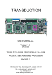
3(%
Micro ATX motherboard
User’s Manual
Edition: 1.0
2009/07/28
P E B - 7 6 1 3 User’s Manual
Copyright
Copyright 20 09. All rights reserved. This document is copyrighted and all rights are
reserved. The information in this document is subject to change without prior notice to make
improvements to the products.
This document contains pr oprietary information and protected by copyright. No part of this
document may be reproduced, copied, or translated in any form or any means without prior
written permission of the manufacturer.
All trademarks and/or registered trademarks contains in this document are property of their
respective owners.
Disclaimer
The company shall not be liable for any incidental or consequential damages resulting from
the performance or use of this product.
The company does not issue a warranty of any kind, express or imp lied, including without
limitation implied warranties of merchantability or fitness for a particular purpose.
The company has the right to revise the manual or include changes in the specifications of
the product described within it at any time without notice and without obligation to notify any
person of such revision or changes.
Trademark
All trademarks are the property of their respective holders.
2
P E B - 7 6 1 3 User’s Manual
Packing List
Please check package component before you use our products.
Hardware: PEB-7613
Micro ATX motherboard x 1
Cable Kit:
SATA Cable x 2
DB25 & DB9 cable x 1
Floppy flat cable x 1
I/O Shield x 1
RAID drivers Disc for Windows XP
Other Accessories:
Divers CD (including User’s Manual) x 1
3
User’s Manual
Index
Chapter1 <Introduction> ............................................................7
1.1 <Product Overview> .............................................................................................7
1.2 <Product Specification> ........................................................................................8
1.3 <Block Diagram> ................................................................................................10
1.4 <Mechanical Drawing > ...................................................................................... 11
Chapter 2 <Hardware Setup>.................................................12
2.1 <Connector Location>.........................................................................................12
2.2 <Component Placement> ...................................................................................13
2.3 <Jumper Reference> ..........................................................................................14
2.4 <Connector Reference>......................................................................................15
2.4.1 <Internal Connectors> ..............................................................15
2.4.2 <External Connectors> .............................................................15
2.5 <CPU and Memory Setup> .................................................................................16
2.5.1 <CPU installation> ...................................................................16
2.5.2 <Memory installation> ..............................................................17
2.6 <CMOS Setup>...................................................................................................18
2.7 <Serial ATA installation>......................................................................................19
2.8 <Floppy Installation> ...........................................................................................20
2.9 <LAN installation>...............................................................................................21
2.10 <Onboard Display Interface> ............................................................................22
2.10.1 <Analog Display> ..................................................................22
2.11 <Audio Installation>...........................................................................................23
2.12 <GPIO and SMBUS interface> .........................................................................25
2.13 <USB Installation> ............................................................................................26
2.14 <Power and Fan Installation> ...........................................................................28
2.15 <Serial Port> .....................................................................................................30
2.16 <Switch and Indicator> .....................................................................................33
4
User’s Manual
Chapter 3 <System Configuration> .......................................35
3.1 <SATA configuration>..........................................................................................35
3.2 <SATA RAID Configuration> ...............................................................................36
3.3 <Audio Configuration> ........................................................................................40
3.4 <Video Memory Setup> ......................................................................................41
3.5 <Display Properties Setting>...............................................................................43
Chapter 4 <BIOS Setup> .........................................................45
Appendix A <I/O Port Pin Assignment> ................................47
A.1 <Serial ATA Port>................................................................................................47
A.2<Floppy Port> ......................................................................................................47
A.3 <IrDA Port>.........................................................................................................48
A.5 <VGA Port> ........................................................................................................49
A.6 <LAN Port>.........................................................................................................49
Appedix B <System Resources> ...........................................50
B.1 <I/O Port Address Map> .....................................................................................50
B.2 <Memory Address Map> ....................................................................................52
B.3 <System IRQ Resources> ..................................................................................53
Appedix C <Flash BIOS>.........................................................54
C.1 <BIOS Auto Flash Tool> ................................................................................54
C.2 <Flash Method> ..............................................................................................54
Appendix D <Programming GPIO’s> ....................................55
Appendix E <Watch Dog timer Setting >..............................56
Contact Information ...................................................................57
5
User’s Manual
(This Page is Left for Blank)
6
User’s Manual
Chapter1 <Introduction>
1.1 <Product Overview>
PEB-7613 is the motherboard with last Intel desktop technology with Micro ATX form factor .
Based on Intel® Q45 and ICH10DO, the board integrates a new Core 2 Quad / Core 2 Duo
Celeron processor 775-pin socket, DDR3 memory socket, Intel® Graphic Media Accelerator
4500 technology, Serial ATA II with RAID function for a powerful desktop system.
Intel® LGA775 processor
The Intel® Core 2 Quad / Core 2 Duo / Celeron proc
essor no w com es with a ne w form
factor with 775-pin PLGA package, for 800/1066/1333MHz front-side-bus, 12MB L2 cach e,
for 65nm a nd 45nm manufacturing technology, the P LGA processor without pin h eader on
solder side can make user installing the processor on the socket easier.
Intel® Q45 and ICH10DO chipset
The Intel Q45 integrates DD R3 800/1066MHz for memory, and Graph ic Media Accelerator
(GMA) 4500 t echnology for new graphic e ngine. It can p rovide up to 1024MB of frame
buffer when you install over 1GB of system memory. The ICH10DO integrates with up to 12
USB2.0 interfaces, and serial ATA II interface with RAID function.
PCI-Express interface
PEB-7613 integrates one x16 and one x4 PCI-Express interface, it can provide up to 8GB/s of
bandwidth.
Flexible Extension Interface
The board provides Two PCI-slot for graphics card, it also can support PCI-slot for LAN card
or other devices. The board also provides mini-PCI socket and ISA slot.
7
User’s Manual
1.2 <Product Specification>
General Specification
Form Factor
CPU
Memory
Chipset
BIOS
Green Function
Watchdog Timer
Real Time Clock
Serial ATAII
Micro ATX motherboard
Intel® Core 2 Quad / Core 2 Duo / Celeron processor
With LGA775 socket
Package type: LGA 775
Front side bus: 800/1066/1333MHZ (200/266/333MHz x 4)
2 x 240-pin DDR3 800/1066MHz SDRAM up to 4GB
Unbufferred, none-ECC memory supported only
Intel® Q45 (Northbridge) and ICH10DO (Southbridge)
Phoenix-Award v6.00PG 8Mb SPI flash BIOS
Power saving mode includes doze, standby and suspend modes.
ACPI version 1.0 and APM version 1.2 compliant
System reset programmable watchdog timer with 1 ~ 255 sec./min.
of timeout value
Intel® ICH10DO built-in RTC with lithium battery
Intel® ICH10DO integrates 6 Serial ATA II interface
RAID 0, 1,5,10 Intel Matrix Storage Technology supported
Multi-I/O Port
Chipset
Serial Port
USB Port
Floppy Port
IrDA Port
K/B & Mouse
GPIO
Smart Fan
Intel® 82801JDO ( ICH10DO) with Winbond® W83627DHG
Controller
Five RS-232 and one RS232/422/485 serial ports
Twelve Hi-Speed USB 2.0 ports with 480Mbps of transfer rate
One Floppy port
One IrDA compliant Infrared interface supports SIR
External PS/2 keyboard and mouse ports on rear I/O panel
One 12-pin Digital I/O connector with 8-bit programmable I/O
Interface
One CPU fan connectors for fan speed controllable
VGA Display Interface
Chipset
Frame Buffer
Display Type
Connector
Intel® Q45 GMA4500 (Graphic Memory Controller Hub)
Up to 1024MB shared with system memory
CRT, LCD monitor with analog display
External DB15 female connector on rear I/O panel
Ethernet Interface
Controller
Type
Connector
8
Two Intel 82574L Gigabit Ethernet controller
Triple speed 10/100/1000Base-T
Auto-switching Fast Ethernet
Full duplex, IEEE802.3U compliant
Two External RJ45 connectors with LED on rear I/O panel
User’s Manual
Audio Interface
Chipset
Interface
Connector
Intel® ICH10DO with Realtek ALC888HD Audio
Intel High Definition Audio compliance
2 channels sound output
External 3 phone jack for 2 channel audio on rear I/O panel
External SPDIF connector on rear I/O panel
Internal 10-pin header for line-out, MIC-in, 4-pin header for CD-IN
Expansive Interface
PCI-Express One
PCI
Mini PCI
ISA
16x PCI-Express slot (compatible with x1 slot)
(16x PCI-Express slot no supply 1x PCI-Express RAID Card)
One 4x PCI-Express slot (compatible with x 1 slot)
Up to 8GB/s of transfer bandwidth
Power supply: +3.3V, +12V
Two-PCI slot (32-bit, 33MHz)
Power supply: +3.3V, +5V, +12V, -12V
One Mini-PCI socket TYPE III A (32-bit, 33MHz)
Power supply: +3.3V, +5V
One ISA slots (without DMA supported)
Power and Environment
Power
Requirement
Dimension
Temperature
Standard ATX 24-pin (20-pin is compatible) power supply
Additional +12V 4-pin power connector
244 (L) x 244 (H) mm
Operating within 0 ~ 60OC (32 ~ 140OF)
Storage within –20 ~ 85OC (-4 ~ 185OF)
p
P
P
p
P
p
P
p
Ordering Code
PEB-7613
Support Intel Core 2 Quad LG A775 with DDRIII, Onboard VGA
Dual Intel Gigabit LAN, 12 x USB2.0, HD Audio, 6 x COM , GPI O,
SATA and ISA .
9
User’s Manual
1.3 <Block Diagram>
Intel Core 2 Quad / Core Due with 775 Pin PLGA
VGA
Intel Q45
PCIE 16x Slot
4 x 240-pin DDR3
800/1066MHz up
to 8GB
6 x Serial ATAII ports
12 x USB2.0 ports
Intel 82574L
2 x GLAN
ICH10DO
HD Audio
Mini-PCI slot
2 x PCI Slot
2 x Serial ports
SPI
W83628 + W83629
1 x Floppy port
8-bit GPIO
PCI bus
BIOS
ISA Slot
IrDA
COM3~6
10
User’s Manual
1.4 <Mechanical Drawing >
Unit: inch
11
User’s Manual
Chapter 2 <Hardware Setup>
2.1 <Connector Location>
CN_COM4
CN_AUDIO
CDIN
CN_LPT
CN_COM5/6
CN_IR
CN_DIO
CN_12V
Mini-PCI
CPUFAN
CN_SMBUS
JFRNT
SYSFAN
USB 1/2/3/4 SA TA 1/2/3/4/5/6
12
FDD
ATX
User’s Manual
2.2 <Component Placement>
PCI-Express
ISA
PCI
DIM
Mini-PCI
PS2
USB_RJ45_1/2
COM1 + CRT
COM2+COM3
Audio SPDIF
13
User’s Manual
2.3 <Jumper Reference>
Jumper
JRTC
JP1
JP2
JAT
JCSEL1
JCSEL2
Function
CMOS Operating/Clear Setting (Page 18)
COM1 signal mode switch (For Pin-1 & Pin-9) (Page 32)
COM2 signal mode switch (For Pin-1 & Pin-9) (Page 32)
Power mode select
CN_COM2 RS-232 RS422 RS485 Setting (Page 32)
CN_IR IrDA Setting (Page 32)
JAT
3
1
Jumper: JAT
Type: Onboard 3-pin jumper
JAT
1-2
2-3
Default setting
14
Mode
AT Power mode
ATX Power mode
User’s Manual
2.4 <Connector Reference>
2.4.1 <Internal Connectors>
Connector
Function
CPU
LGA775 CPU socket
DDR3_A1/A2/B1/B2 240 –pin DDR2 SDRAM DIMM socket
FDD
34-pin slim type floppy connector
S_ATAII1/2/3/4/5/6 7-pin
Serial ATA II connector
ATX
24-pin power supply connector
CN_12V
4-pin +12V additional power supply connector
CN_AUDIO
5 x 2-pin audio connector
CDIN
4-pin CD-ROM audio input connector
CN_DIO
6 x 2-pin digital I/O connector
CN_USB1/2/3/4
10-pin USB connector
CPUFAN
4-pin CPU cooler fan connector
SYSFAN
3-pin system cooler fan connector
NBFAN
3-pin Northbridge cooler fan connector
CN_IR
5-pin IrDA connector
CN_SMBUS
5-pin SMBUS connector
JFRNT
14-pin front panel switch/indicator connector
PCI1/2
120-Pin PCI socket
CN_COM3/4/5
5 x 2-pin com connector
Remark
2.4.2 <External Connectors>
Connector
PS2
CRT+COM1
USB_RJ45_1/2
COM 2/3
AUDIO Audio
SPDIF
Function
PS/2 Keyboard/Mouse connector
DB15 VGA + Serial port connector
Dual USB and one RJ45 LAN Port
Serial port connector
connectors
SPDIF digital audio output connector
Remark
15
User’s Manual
2.5 <CPU and Memory Setup>
2.5.1 <CPU installation>
PEB-7613 has a LGA775 CPU socket on board; ple ase ch eck follo wing ste ps to inst all th e
processor properly.
Attention
If PEB-7613 need RMA please Keep CPU socket cover on the CPU Socket.
Warning
If CPU Socket internal Pin damage We could not provide warranty.
Intel® Quad Core 2 Quad / Core 2 Duo
Cleron processor
Package type: 775 pin PLGA
FSB:/800/1066/1333MHz
Manufacturing: 65nm / 45nm
1. Lift this bar
Intel Hyper Threading Technology and
Core 2 Duo Quad / Duo supported
Checked point
3. Place the CPU on the top of
2. Uncover this plate
4. Lock this bar
the pins
3. Cover this plate
Notice: Please place the CPU on the pins tenderly to avoid bending the pins
16
CPU Inst allation
User’s Manual
2.5.2 <Memory installation>
PEB-7613 has four 240-pin DDR3 DIMM support up to 8GB of memory capacity. The memory
frequency supports 800/1066 MHz. Only Non-ECC memory is supported.
DDRIII A1/A2/B1/B2
144-pin
96-pin
Please check the pin number to match the socket side well
before installing memory module.
17
User’s Manual
2.6 <CMOS Setup>
The board’s data of CMOS can b e setting in BIOS. If th e bo ard refus es to boot d ue to
inappropriate CMOS setting s, here is ho w to proceed to clear (r eset) t he CMOS to its
default values.
Jumper: JRTC
Type: Onboard 3-pin jumper
JRTC
1-2 Clear
2-3
Default setting
Mode
CMOS
Normal Operation
3
1
JRTC
18
CMOS Se tup
User’s Manual
2.7 <Serial ATA installation>
PEB-7613 has four Serial A TA II interfaces with RAID function, the transfer rate of the Serial
ATA II can be up to 300MB/s. Please go to http://www.serialata.org/ for more about Serial
ATA technology information. Based on Intel® ICH10DO, it supports Intel® Matrix Storage
Technology with combi nation of RAID 0, 1,5 an d 10. T he mai n featu res of RAID on
ICH10DO are listed below:
1.
Supports for up to RAID volumes on a single, two-hard drive RAID array.
2.
Supports for two, two-hard drive RAID arrays on any of six Serial ATA ports.
3.
Supports for Serial ATA ATAPI devices.
4.
Supports for RAID spares and automatic rebuild.
5.
Supports on RAID arrays, including NCQ and native hot plug.
For more information please visit Intel’s official website.
For more abo ut the s ystem setup for Serial
A TA, pleas e check the c hapter of SA TA
configuration.
SATA1/2/3/4/5/6
Serial ATA installation
19
User’s Manual
2.8 <Floppy Installation>
PEB-7613 has one 34-pin floppy interface.
FDD
20
Floppy Ins tallation
User’s Manual
2.9 <LAN installation>
The board integrates with two Intel 82574L Gigabit Ethernet controllers, as the PCI Express
bus. T he Intel 82574L support s triple spe ed of 10/100/1000Bas e-T, with IEEE802.3
compliance and Wake-On-LAN supported.
LAN2
LAN Installation
LAN1
21
User’s Manual
2.10 <Onboard Display Interface>
Based on Intel Q45 chipset with built-in graphics, the board provides one DB15 Connector
on real external I/O port
2.10.1 <Analog Display>
Please connect your CRT or LCD mon itor with DB15 male connector to the onb oard DB15
female connector on rear I/O port
CRT
22
User’s Manual
2.11 <Audio Installation>
The board integrates onboard audio interface with REALTEK ALC888 codec, with Intel next
generation of audio standard as High Definition Audio, it offers more vivid sound and other
advantages than former HD audio compliance.
The main specifications of ALC888 are:
High-performance DACs with 100dB S/N ratio
2 DAC channels support 16/20/24-bit PCM format for 2 audio solution
16/20/24-bit S/PDIF-OUT supports 44.1K/48K/96kHz sample rate
Compatible with HD
Meets Microsoft WHQL/WLP 2.0 audio requirements
The board provides 2 channels audio phone jacks on rear I/O port, Line-in/MIC-in port s for
front I/O panel through optional cable.
CN_AUDIO
1
9
10
2
CDIN
4
1
23
User’s Manual
Connector: CN_AUDIO
Type: 10-pin (2 x 5) header (pitch = 2.54mm)
Pin
Description
Pin
1 MIC_L
3 MIC_R
5 Speaker_R
7 SENSE
9 Speaker_L
Description
2 Ground
4 ACZ_DET
6 MIC
Detect
8 N/C
10
Speaker Detect
Connector: CDIN
Type: 4-pin header (pitch = 2.54mm)
Pin
Description
1
CD – Left
2 Ground
3 Ground
4
CD – Right
LINE-IN
LINE-OUT
MIC-IN
24
Rear I/O phone jacks
User’s Manual
2.12 <GPIO and SMBUS interface>
The board provides a pr ogrammable 8-bit digital I/O interface, and a
SMBUS (S ystem
management bus) interface for control panel application.
Connector: CN_DIO
Type: onboard 2 x 6-pin header (pitch=2.0mm)
Pin
Description
1 Ground
3 GP10
5 GP11
7 GP12
9 GP13
11 VCC
Pin
Description
2 Ground
4 GP14
6 GP15
8 GP16
10
GP17
12 +
12V
CN_SMBUS
5
1
12
2
11
1
CN_DIO
Connector: CN_SMBUS
Type: 5-pin header for SMBUS Ports (pitch = 2.54mm)
Pin
Description
1 VCC
2 N/C
3 SMBDAT
A
4 SMBCLK
5 Ground
25
User’s Manual
2.13 <USB Installation>
PEB-7613integrates eight USB2.0 ports. The specifications of USB2.0 are listed below:
Interface
Controller Intel
Transfer Rate
USB2.0
ICH10DO
Up to 480Mb/s
Voltage 5V
The Intel ® ICH10DO c ontains t wo En hanced H ost Co ntroller I nterface (EHCI) an d fi ve
Universal H ost Controll er Interfaces (UHCI ), it can determine
whether yo ur connected
device is for USB1.1 or USB2.0, and change the transfer rate automatically.
USB
26
User’s Manual
Connector: CN_USB1/2/3/4
Type: 10-pin (5 x 2) header (pitch = 2.54mm)
Pin
Description
1 VCC
3 Data05 Data0+
7 Ground
9 Ground
10
Pin
Description
2 VCC
4 Data16 Data1+
8 Ground
10
N/C
9
1
2
CN_USB1/2/3/4
27
User’s Manual
2.14 <Power and Fan Installation>
The PEB-7613 p rovides a st andard A TX po wer sup ply with 24-pin A TX connect or an d
additional 12 V connector , an d the boar d provid es one 4-pin fan conne ctors supporti ng
smart fan for CPU cool er and one 3- pin cooler fan conn ectors for s ystem and N orthbridge
chip. The 4-pin CN_12V additional power connector is necessary for CPU powering; please
connect this well before you finishing the system setup.
CN_12V
1
3
2
4
CPUFAN
1
4
SYSFAN
1
3
1
2
28
23
ATX
24
User’s Manual
Connector: ATX
Type: 24-pin ATX power connector
PIN assignment
1 3.3V
2 3.3V
3 GND
4 5V
5 GND
6 5V
7 GND
8 PW
_OK
9 5V_SB
10 12V
11 12V
12 3.3V
13
3.3V
14
-12V
15
GND
16
PS_ON
17
GND
18
GND
19
GND
20
-5V
21
5V
22 5V
23
5V
24 GND
Connector: CN_12V
Type: 4-pin standard Pentium 4 additional +12V power connector
Pin
Description
1 Ground
3+
12V
Connector: CPUFAN
Type: 4-pin fan wafer connector
Pin
Description
1 Ground
3
Fan Speed Detection
Connector: SYSFAN
Type: 3-pin fan wafer connector
Pin Description
Pin
1 Ground
2
Pin
2
4
Description
Ground
+12V
Pin
2
4
Description
+12V
Fan Control
Description
+12V
Pin
3
Description
Sense
29
User’s Manual
2.15 <Serial Port>
The board su pports T hree RS232 s erial po rt and on e jum per sel ectable RS232/422/485
serial ports. T he jum per JC SEL1 & JCSE L2 ca n let you confi gure th e commun icating
modes for COM2.
COM1
COM2
COM3
Connector: COM2
Type: 9-pin D-sub male connector on bracket for COM2
Pin
Description
1 DCD/422T
X-/4853T
XD/422RX+
5 GND
7 RT
S
9 RI
30
Pin
Description
2
RXD/422TX+/485+
4 DT
R/422RX6 DSR
8 CT
S
10
N/C
User’s Manual
Setting RS-232 & RS-422 & RS-485 for COM2C
JP1
2 6
1
2
JCSEL2
11
12
1 5
JP2
2 6
1 5
JCSEL1
2
8
1
7
31
User’s Manual
Function
SIR
RS-422
JCSEL1
JCSEL2
2
12
1
11
2
12
7
1
11
2
8
2
12
1
7
1
11
2
12
1
11
2
8
1
7
2
8
1
RS-485
RS-232
2
8
1
7
Default setting : JCSEL1: (1-2) JCSEL2: (1-3, 2-4, 7-9, 8-10)
Jumper: JP1/JP2 (COM1/2)
Type: onboard 6-pin header
Power Mode
JP1/JP2
Pin 1 with 5V Power
1-3,4-6
Pin 9 with 12V Power
Default setting: 3-5, 4-6
32
2
6
1
5
2
6
1
5
2-4,3-5
User’s Manual
2.16 <Switch and Indicator>
The JFRNT p rovides fro nt co ntrol panel of th e bo ard, such a s po wer bu tton, re set and
beeper, etc. Please check well before you connecting the cables on the chassis.
Connector: JFRNT
Type: onboard 14-pin (2 x 7) 2.54-pitch header
Function
SATA LED
Reset
Power
Button
Signal
PIN
Signal
HDLED+ 1
2
PWDLED+
HDLED- 3
4
N/C
Reset+ 5
6
PWDLED-
Reset- 7
8
SPKIN+
N/C 9
10
N/C
12
N/C
14
SPKIN-
PWRBT+ 1
PWRBT- 13
1
Function
Power
LED
Speaker
JFRNT
13
14
2
1
33
User’s Manual
(This Page is Left for Blank)
34
User’s Manual
Chapter 3 <System Configuration>
3.1 <SATA configuration>
SATA Mode:
This option can let you select whether the Serial ATA hard drives would work under normal
IDE mode or RAID mode. The RAID mode need more than one HDD is applied.
35
User’s Manual
3.2 <SATA RAID Configuration>
The board integrates Intel ® ICH10DO with RAID function for Serial
ATA II drives, and
supports the configurations below:
RAID 0 (S tripping): Two ha rd driv es o perating as o ne drive for optimized data R/ W
performance. It needs two unused drives to build this operation.
RAID 1 (Mirroring): Copies the data from first drive to second drive for dat a security, and if
one drive fails, the system would access the applications to the workable drive. It needs two
unused drives or one used and one unused drive to build this operation. The second drive
must be the same or lager size than first one.
RAID 5 (striping with parity)
A RAID 5 arra y c ontains three or
more har d dr ives where the
data is divid ed i nto
manageable bl ocks call ed stri ps. Parit y is a mathematical method for rec reating data th at
was lost from a single drive, which increases fault-tolerance. The data and parity are striped
across all the hard drives in the array. The parity is striped in a rotating sequence to reduce
bottlenecks associated with the parity calculations.
RAID 10 (RAID 0+1)
A RAID 10 array uses four hard drives to create a combination of RAID levels 0 and 1. The
data is striped across a two-drive array forming the RAID 0 compo nent. Each of the drive s
in the RAID 0 array is then mirrored by a RAID 1 component.
Intel Matrix Storage Technology: This technology would allow you to use RAID 0+1 mode
on only two drives (4 drives needed on traditional RAID 0+1). It will create two partitions on
each hard drive to simulate RAID 0 and RAID 1. It also can let you modify the partition size
without re-formatted.
For more information of Intel Matrix Storage Technology, please visit Intel’s website.
If you need to inst all an op eration s ystem on the RAID s et, pleas e us e the driv er d isk
attached in the package when it informs you to obtain the RAID drivers.
36
User’s Manual
Please press <CTRL+I> to enter the RAID configuration menu.
You can setup the RAID under oper
ation s ystem for Microsof t® W indows XP SP1 or
Windows 2000 SP4 version, please install the Intel® Application Accelerator Ver.4.5 later to
support RAID configuration with Intel® Matrix Storage Technology.
37
User’s Manual
1. After installing Intel Application Accelerator, please execute Intel® Storage Utility.
Demo configuration for 2 SATA Drives and
set as Intel Matrix Storage Technology set
2. Select Actions to Create RAID Volume
Rename the Volume name
Select RAID Level as 0
Left as default
38
User’s Manual
3. Please select two hard drives to prepare to set the RAID volume
4. Specify the Volume size
Tune this bar to specify
the volume size, if you
specify the volume size
lower than maximum,
you can create a second
volume for another
RAID set.
(Make RAID 0+1 on only
two hard drives)
5. Repeat the step 1 to create second volume as RAID Level 1.
For other configuration set please click Help on tool bar.
39
User’s Manual
3.3 <Audio Configuration>
The board integrates Intel ® ICH10DO with REAL TEK® ALC888 cod ec. It can suppo rt
2-channel sound under system configuration. Please follo w the steps below to setu p your
sound system.
1.
Install REALTEK HD Audio driver.
2.
Lunch the control panel and Sound Effect Manager.
3.
Select Speaker Configuration
4. Select the sound mode to meet your speaker system.
40
User’s Manual
3.4 <Video Memory Setup>
Based on Intel ® Q45 chip set with GMA (Graphic Me dia Accelerator) 4500, the boa rd
supports Intel ® DVMT (D ynamic V ideo M emory Technology) 3.0, which would allow the
video memory be triggered up to 384MB.
To support DVMT, you need to install the Intel GMA4500 Driver with supported OS.
BIOS Setup:
On-Chip Frame Buffer Size:
This item can let you select video memory which been allocated for legacy VGA and SVGA
graphics support and compatibility. The available option is 32MB and 128MB.
41
User’s Manual
Total GFX Memory Size:
This item can let you select a static amount of page-locked graphics memory; which will be
allocated dur ing driv er in itialization. Onc e you se lect the memory am ount, it will be no
longer available for system memory.
DVMT Memory Size:
This item can let you sel ect a maximum si ze of dy namic amount usage of video memory ,
the s ystem would co nfigure the vid eo mem ory depends o n your a pplication, this item i s
strongly recommend to be selected as MAX DVMT.
Fixed + DVMT Memory Size:
You can select the fixed amount and the DVMT amount at the sam e time for a guaranteed
video memory and additional dynamic video memory
Notice:
1.
42
The On-Chip Frame Buffer Size would be included in the Total GFX Memory Size.
User’s Manual
3.5 <Display Properties Setting>
Based on Intel Q45 GMCH with GMA4500 (Graphic Media Accelerator), the board supports
two DACs for display device as different resolution and color bit.
Please install the Intel Graphic Driver before you starting setup display devices.
1. Click right button on the desktop to lunch display properties
2. Click Advanced button for more specificity setup.
Click Graphics Properties... for
advanced setup
3. This setup options can let you define each device settings.
43
User’s Manual
Click Monitor to setup the CRT
monitor for Col ors, Resolution
and Refresh Rate
Click
Intel® Dual
Display
Clone t o se tup the d ual
display mode as same screen
Set the main display device here
Click Extended Desk top to
setup the d ual displa y m ode
as different screen display
44
LV-676 User’s Manual
Chapter 4 <BIOS Setup>
The motherbo ard uses the Award BIOS fo r the s ystem config uration. T he A ward
BIOS in the si ngle boar d co mputer is a cust omized versi on of the industrial stand ard
BIOS for IBM PC AT-compatible computers. It supports Intel x8 6 and compatible CPU
architecture b ased processors and c omputers. The BIOS provi des cri tical lo w-level
support for the system central processing, memory and I/O sub-systems.
The BIOS setup progr am of the single bo ard computer l et the customers modif y the
basic confi guration settin g. T he settings are stored in a dedic ated b attery-backed
memory, NV RAM, retains the in formation w hen the po wer is turned off. If the batter y
runs out of the power, then the settings of BIOS will come back to the default setting.
The BIOS section of the manual is subject to change without notice and is provided here
for reference p urpose onl y. The settings an d c onfigurations of the BIOS are current at
the time of print, and therefo re they may not be exactly the same as that displa yed on
your screen.
To activate CMOS Setup program, press <DEL> key i mmediately after you turn on
the system. The following message “Press DEL to enter SET UP” should appear in th e
lower left hand corner of your screen. When you enter the CMOS Setup Utility, the Main
Menu will be di splayed as Figure 4-1. You can use arrow keys to s elect your function,
press <Enter> key to accept the selection and enter the sub-menu.
Figure 4-1 CMOS Setup Utility Main Screen
45
User’s Manual
(This Page is Left for Blank)
46
User’s Manual
Appendix A <I/O Port Pin Assignment>
A.1 <Serial ATA Port>
1
Connector: SATA_1/2/3/4/5/6
7
Type: 7-pin wafer connector
1
2
3
4
5
6
7
GND RSATA_TXP1 RSATA_TXN1 GND RSATA_RXN1 RSATA_RXP1 GND
33
1
34
2
A.2<Floppy Port>
Connector: FDD
Type: 34-pin connector
Pin
Description
1
Ground
3 Ground
5 Ground
7 Ground
9
Ground
11 Ground
13 Ground
15 Ground
17 Ground
19 Ground
21 Ground
23 Ground
25 Ground
27 Ground
29 Ground
31 Ground
33 Ground
Pin
Description
2
DRIVE DENSITY SELECT 0
4 N/C
6 N/C
8 INDEX10
MOTOR ENABLE A12 N/C
14 DRIVER
SELECT A16 N/C
18 DIRECT
ION20 ST
EP22 W
RITE DATA24 W
RITE GATE26 T
RACK 028 W
RITE PROTECT30 READ
DATA32 HEAD
SELECT34 DISK
CHANGE-
47
User’s Manual
A.3 <IrDA Port>
Connector: CN_IR
Type: 5-pin header for SIR Ports
1
5
Pin
Description
1 VCC
2 N/C
3 IRRX
4 Ground
5 IRT
X
A.4 <Serial Port>
1
2
3
4
5
Connector: COM1/2/3
Type: 9-pin D-sub male connector on bracket
Pin
Description
Pin
Description
1 DCD
6 DSR
2 SIN
7 RT
S
3 SO
8 CT
S
4 DT
R
9 RI
5 Ground
9
1
10
2
Connector: COM4/5/6
Type: 9-pin header connector for COM4
Pin
Description
Pin
Description
1 DCD
6 DSR
2 SIN
7 RT
S
3 SO
8 CT
S
4 DT
R
9 RI
5 Ground
48
6
7
8
9
User’s Manual
A.5 <VGA Port>
1
2
3
4
5
Connector: CRT
Type: 15-pin D-sub female connector on bracket
6
11
12
13
14
15
10
Pin
Description
1 RED
2 GREEN
3 BLUE
4 N/C
5 Ground
Pin
6
7
8
9
10
Description
Ground
Ground
Ground
+5V
Ground
Pin
11
12
13
14
15
Description
N/C
DDC_DA
HSYNC
VSYNC
DDC_CLK
A.6 <LAN Port>
Connector: RJ451/2
Type: RJ45 connector with LED on bracket
Pin
Description
Pin
Description
1
TRD0+ T
6
TRD1- T
2
3
4
5
RD0- TRD1+ TRD2+ TRD27
8
RD3+ TRD3-
9
10
NC
NC
49
User’s Manual
Appedix B <System Resources>
B.1 <I/O Port Address Map>
50
User’s Manual
51
User’s Manual
B.2 <Memory Address Map>
52
User’s Manual
B.3 <System IRQ Resources>
53
User’s Manual
Appedix C <Flash BIOS>
C.1 <BIOS Auto Flash Tool>
The board is based on Award BIOS and can be updated easily by the BIOS auto flash
tool. You can download the tool online at the address below:
http://www.award.com
TU
UT
T
File name of the tool is “awdflash.exe”, it’s the utility that can write the data into the BIOS
flash ship and update the BIOS.
C.2 <Flash Method>
1. Please make a bootable floppy disk.
2. Get the last .bin files you want to update and copy it into the disk.
3. Copy awardflash.exe to the disk.
4. Power on the system and flash the BIOS. (Example: C:/ awardflash XXX.bin)
5. Re-star the system.
Any question about the BIOS re-flash please contact your distributors or visit the
web-site at below:
54
User’s Manual
Appendix D <Programming GPIO’s>
The GPIO’can be programmed with the MSDOS debug program using simple
IN/OUT commands.The following lines show an example how to do this.
GPIO0…..GPIO7 bit0……bit7
-o 2E 87
;enter
configuration
;enale
GPIO function
-o 2E 87
-o 2E 07
-o 2F 09
-o 2E 30
-o 2F 02
;enable
GPIO configuration
-o 2E F0
-o 2F xx
;set GPIO as input/output; set ‘1’ for input,’0’for output
-o 2E F1
-o 2F xx
;if
set GPIO’s as output,in this register its value can be set
Optional :
-o 2E F2
-o 2F xx
; Data inversion register ; ‘1’ inverts the current valus of the bits ,’0’
leaves them as they are
-o 2E 30
-o 2F 01
; active GPIO’s
For further information ,please refer to Winbond W83627DHG datasheet.
55
User’s Manual
Appendix E <Watch Dog timer Setting >
The watchdog timer makes th e system auto-reset while it stop s to work for a perio d. The
integrated watchdog timer can be setup as system reset mode by program.
Timeout Value Range
- 1 to 255
- Second or Minute
Program Sample
Watchdog timer setup as system reset with 5 second of timeout
2E, 87
2E, 87
2E, 07
2F, 08
Logical Device 8
2E, 30
Activate
2F, 01
2E, F5
Set as Second*
2F, 00
2E, F6
Set as 5
2F, 05
* Minute: bit 3 = 0; Second: bit 3 = 1
You can select Timer setting in the BIOS, after setting the time options, the system will
reset according to the period of your selection.
56
User’s Manual
Contact Information
Any advice or comment about our products and service, or anything
we can help you please don’t hesitate to contact with us. We will do
our best to support you for your products, projects and business. P
Portwell Technology Inc.
Address
Website
Contact Information
44200 Christy Street, Fremont, CA 94538
http://www.portwell.com
TU
57