1
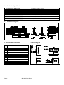
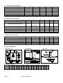
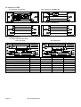
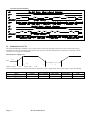
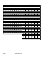
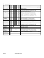
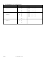
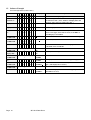
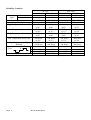
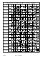
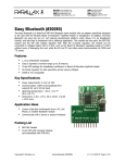
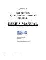
QP-5515
DOT MATRIX
LIQUID CRYSTAL DISPLAY
MODULE
USER’S MANUAL
Distributed by:
Electus Distribution Pty Ltd.
100 Silverwater Road
Silverwater, NSW, 2128
AUSTRALIA
Phone: 1300 738 555
FAX: 1300 738 500
Email: [email protected]
http://www.electusdistribution.com.au
Page: 1
QP-5515 Data Sheet
CONTENTS
1.
2
3.
4.
5.
6.
7.
8.
9.
10.
Mechanical Specification
Mechanical Diagram
Interface Pin Connections
Block Diagram
Absolute Maximum Rating
Electrical Characteristics
Optical Characteristics
Optical Definitions
Display Address
Interface to MPU
10.1 Interface to Z-80 CPU
10.2 Interface to MC6800 CPU
10.3 Interface to 4-bit CPU ( HMCS43C )
10.4 Interface to HD6805 MP
PAGE
3
3
3
3
4
4
4
4
4
5
5
5
5
5
11. Timing Control
11.1 Write and Read Operation
11.2 Busy flag check timing
6
6
6
12.
13.
14.
15.
16.
17.
6
8
9
10
11
12
Initialization of LCM
Instruction Set
User Font Patterns
Software Example
Reliability Condition
Character Generator ROM Map
Page: 2
QP-5515 Data Sheet
1.
Mechanical Specification
ITEM
NUMBER OF CHARACTERS
CHARACTER FORMAT
MODULE DIMENSION
VIEWING DISPLAY AREA
ACTIVE DISPLAY AREA
CHARACTER SIZE
CHARACTER PITCH
DOT SIZE
DOT PITCH
DISPLAY
2.
STANDARD VALUE
16 CHARACTERS X 2 LINES
5 X 8 DOTS
85.0 (W) X 30.0 (H) X 9.0 (T)
85.0 (W) X 30.0 (H) X 13.2 (T)
65.0 (W) X 16.0 (H)
56.21 (W) X 10.98 (H)
2.78 (W) X 4.89 (H)
3.53 (W) X 6.09 (H)
0.50 (W) X 0.55 (H)
0.57 (W) X 0.62 (H)
STN , Yellow Green , 1/16 Duty , 6 O‘clock
Mechanical Diagram
3. Interface Pin Connections
NO
1
2
3
4
5
6
7
8
9
10
11
12
13
14
SYMBOL LEVEL
VDD
-VSS
-VO
H/L
RS
H/L
R/W
H/L
E
H,H→L
DB0
H/L
DB1
H/L
DB2
H/L
DB3
H/L
DB4
H/L
DB5
H/L
DB6
H/L
DB7
H/L
A+ (EL1)
-K- (EL2)
--
Page: 3
4. Block Diagram
FUNCTION
DC +5V
GND (0V)
Contrast Adjust
Register select
Read/Write
Enable signal
Data Bit 0
Data Bit 1
Data Bit 2
Data Bit 3
Data Bit 4
Data Bit 5
Data Bit 6
Data Bit 7
A (EL Backlight 1)
K (EL Backlight 2)
QP-5515 Data Sheet
UNIT
--mm
mm
mm
mm
mm
mm
mm
5. Absolute Maximum Ratings
ITEM
OPERATING TEMPERATURE
STORAGE TEMPERATURE
INPUT VOLAGE
SUPPLY VOLTAGE FOR LOGIC
SUPPLY VOLTAGE FOR LCD
STATIC ELECTRICITY
SYMBOL
MIN.
TYPE
MAX.
TOP
0/-20
-+50/+70
TST
-10/-30
-+60/+80
VI
VSS
-VDD
VDD-VSS
-5.0
6.5
VDD-VO
--6.5
Be sure that you are grounded when handing LCM.
UNIT
?
?
V
V
V
6. Electrical Characteristics
ITEM
SUPPLY VOLTAGE FOR LOGIC
SYN
VDD-VSS
MIN.
4.5
----
TYPE
5.0
4.8/5.0
4.4
4.1/3.9
MAX.
5.5
----
UNIT
V
V
V
V
VIH
VIL
VOH
VOL
IDD
CONDITION
-Ta= 0/-20 ?
Ta= 25?
Ta= +50/+70 ?
----VDD=+5V
SUPPLY VOLTAGE FOR LCD
VDD-VO
INPUT HIGH VOLTAGE
INPUT LOW VOLTAGE
OUTPUT HIGH VOLTAGE
OUTPUT LOW VOLTAGE
SUPPLY CURRENT
2.2
0
2.4
---
----3.0
VDD
0.6
-0.4
4.5
V
V
V
V
mA
SYM
?
f
CR
TON
TOFF
CONDITION
CR? 2
CR? 2
----
MIN.
-10
-30
----
TYPE
--5
180
100
MAX.
40
30
-230
150
UNIT
deg.
deg.
-mS
mS
7. Optical Characteristics
ITEM
VIEW ANGLE (V)
VIEW ANGLE (H)
CONTRAST RATIO
RESPONSE TIME
RESPONSE TIME
8. Optical Definitions
Response Time
Contrast Ration
View Angle
9. Display Address
Line 1
Line 2
Page: 4
1
80
C0
2
81
C1
3
82
C2
4
83
C3
5
84
C4
6
85
C5
7
86
C6
8
87
C7
9
88
C8
QP-5515 Data Sheet
10
89
C9
11 12 13 14 15
8A 8B 8C 8D 8E
CA CB CC CD CE
16
8F
CF
10. Interface to MPU
10.1 Interface to Z-80 CPU
10.2 Interface to MC6800 CPU
10.3 Interface to 4-bit CPU ( HMCS43C )
10.4 Interface to HD6805 MP
11. Timing Control
11.1 Write and Read Operation
Write Operation
Read Operation
Item
Enable Cycle Time
Enable Pules Width ( High level )
Enable Rise/Fall Time
Address Set-Up Time ( RS,R/W,E )
Address Hole Time
Data Set-Up Time
Data Delay Time
Data Hold Time
Page: 5
Symbol
tCYCE
PWEH
tER,tEF
tAS
tAH
tDSW
tDDR
tDHR
QP-5515 Data Sheet
Limit (Min.)
1000
450
-100
10
100
-20
Limit (Max.)
--25
---190
--
Unit
ns
ns
ns
ns
ns
ns
ns
ns
11.2 Busy flag check timing
Note : IR7, IR3 : Instruction 7th bit , 3rd bit ; AC3 : Address Counter 3rd bit.
12. Initialization of LCM
The LCM automatically initializes ( reset ) when power is turned on using the internal reset circuit. If the power supply
conditions for correctly operating of the internal reset circuit are not met, initialization by instruction is required. Use the
procedure is next page for initialization.
Internal Power Supply reset
4.5V
Vcc
0.2V
toff
?
?
trcc
? - - - - - - ?
(Note 1) 10 ms ? trcc ? 0.1 ms , toff ? 1 ms.
(Note 2) toff stipulates the time of power OFF for momentary power supply dip or when power supply cycles ON and OFF.
Item
Power supply rise time
Power supply off time
Page: 6
Symbol
trcc
toff
Test condition
---
QP-5515 Data Sheet
Limit (Min.)
0.1
1
Limit (Max.)
10
--
Unit
ms
ms
RS
0
RS
0
RS
0
RS
0
RS
0
RS
0
RS
0
(a) 8-bit interface
(b) 4-bit interface
Power ON
?
Wait more than 15ms after VDD rises to 0.9VDD
?
Function Set
R/W DB7 DB6 DB5 DB4 DB3 DB2 DB1
0
0
0
1
1
*
*
*
?
Wait more than 4.1 ms
?
Function Set
R/W DB7 DB6 DB5 DB4 DB3 DB2 DB1
0
0
0
1
1
*
*
*
?
Wait more than 100µ s
?
Function Set
R/W DB7 DB6 DB5 DB4 DB3 DB2 DB1
0
0
0
1
1
*
*
*
?
Wait more than 100µ s or Busy Flag Check
?
Function Set
R/W DB7 DB6 DB5 DB4 DB3 DB2 DB1
0
0
0
1
1
N
F
*
?
Display Off
R/W DB7 DB6 DB5 DB4 DB3 DB2 DB1
0
0
0
0
0
1
0
0
?
Display Clear
R/W DB7 DB6 DB5 DB4 DB3 DB2 DB1
0
0
0
0
0
0
0
0
?
Entry Mode Set
R/W DB7 DB6 DB5 DB4 DB3 DB2 DB1
0
0
0
0
0
0
1
I/D
?
Write data to the DD/CG RAM and set the Instruction
Power ON
?
Wait more than 15ms after VDD rises to 0.9VDD
?
Function Set
RS
R/W
DB7
DB6
DB5
DB4
0
0
0
0
1
1
?
Wait more than 4.1 ms
?
Function Set
RS
R/W
DB7
DB6
DB5
DB4
0
0
0
0
1
1
?
Wait more than 100µ s
?
Function Set
RS
R/W
DB7
DB6
DB5
DB4
0
0
0
0
1
1
?
Wait more than 100µ s or Busy Flag Check
?
Function Set
RS
R/W
DB7
DB6
DB5
DB4
0
0
0
0
1
1
?
Function Set
RS
R/W
DB7
DB6
DB5
DB4
0
0
0
0
1
0
0
0
N
F
*
*
?
Display Off
RS
R/W
DB7
DB6
DB5
DB4
0
0
0
0
0
0
0
0
1
0
0
0
?
Display Clear
RS
R/W
DB7
DB6
DB5
DB4
0
0
0
0
0
0
0
0
0
0
0
1
?
Entry Mode Set
RS
R/W
DB7
DB6
DB5
DB4
0
0
0
0
0
0
0
0
0
1
I/D
S
?
Write data to the DD/CG RAM and set the Instruction
Page: 7
DB0
*
DB0
*
DB0
*
DB0
*
DB0
0
DB0
1
DB0
S
QP-5515 Data Sheet
13. Instruction Set
R R D D D D D D D D
EXECU.
S /W B B B B B B B B
DESCRIPTION
TIME*
7 6 5 4 3 2 1 0
(MAX.)
1.64ms
Clear Display 0 0 0 0 0 0 0 0 0 1 Clears entire display and returns the cursor to home
position ( address 0 ).
1.64ms
Return Home 0 0 0 0 0 0 0 0 1 x Return the cursor to the home position. Also returns
the display being shifted to the original position. DD
RAM contents remain unchanged.
Set cursor move direct and specifies display
40µ s
Entry mode
I
shift.These operations are performed during data
set
0 0 0 0 0 0 0 1 / S rite/read. For normal operation, set S to zero. I/D=1 :
D
increment ; 0 :decrement ;S=1 : accompanies display
shift when data is written, for normal operation, set to
zero.
Set ON/OFF all display(D),cursor ON/OFF(C), and
40µ s
Display
0 0 0 0 0 0 1 D C B blink of cursor position character(B). D=1: ON
ON/OFF
display; 0:OFF display. C=1: ON cursor;0: OFF
control
cursor. B=1: ON blink cursor; 0: OFF blink cursor.
S R
Move the cursor and shift the display without
40µ s
Cursor or
0 0 0 0 0 1 / / x x changing DD RAM contents. S/C=1: Display shift;
Display
C L
0:Cursor move. R/L=1: shift to right; 0: shift to left.
shift
Set the interface data length (DL). Number of display
40µ s
Function
0 0 0 0 1 D N F x x lines (N) and character font (F). DL=1: 8 bits; 0:4 bits.
Set
L
N=1: 2 lines; 0: 1 lines. F=1: 5x10 dots; 0: 5x7 dots.
ACG
Set CG RAM address. CG RAM data is sent and
40µ s
Set CG RAM 0 0 0 1
received after this setting.
address
ADD
Set DD RAM address. DD RAM data is sent and
40µ s
Set DD RAM 0 0 1
received after this setting
address
Reads Busy Flag (BF) indicating internal operation is
1 µ s
Read busy
0 1 B
AC
being performed and reads address counter contents.
flag &
F
BF=1: internally operating. 0: can accept instruction
address
WRITE DATA
Write data into DD RAM or CG RAM.
40µ s
Write Data to 1 0
CG/DDRAM
READ DATA
Read data from DD RAM or CG RAM
40µ s
Read Data for 1 1
CG/DDRAM
FUNCTION
Page: 8
QP-5515 Data Sheet
14. User Font Patterns ( CG RAM Character )
Character Code (DD RAM data)
Hi
76543210
CG RAM Address
543
0000x000
000
0000x001
001
----------------
0000x111
Page: 9
Lo
210
000
001
010
011
100
101
110
111
000
001
010
011
100
101
110
111
----------------
111
000
001
010
011
100
101
110
111
QP-5515 Data Sheet
Character Pattern (CG RAM data)
Hi
765
xxx
xxx
xxx
xxx
xxx
xxx
xxx
xxx
xxx
xxx
xxx
xxx
xxx
xxx
xxx
xxx
4
1
1
1
1
1
1
1
0
1
0
1
0
1
0
0
0
3
1
0
0
1
0
0
0
0
0
1
1
0
1
0
0
0
2
1
0
0
1
1
0
0
0
0
0
1
1
1
1
1
0
1
1
0
0
1
0
1
0
0
0
1
1
0
1
1
0
0
0
0
1
1
0
0
0
1
0
1
0
1
0
1
0
0
0
--------------------------------
Lo
15. Software Example
15.1 8-bit operation ( 8 bits 2 lines )
Function
R R D D D D D D D D
S w 7 6 5 4 3 2 1 0
Display
Power on delay
Description
Function set
0 0 0 0 1 1 0 0 x x
Display OFF
0 0 0 0 0 0 1 0 0 0
Initialization. No display appears.
Sets to 8-bit operation and selects 2-line display and 5x7
dots character font. ( Note: number of display lines and
character fonts cannot be chang after this. )
Turn off display.
Display ON
0 0 0 0 0 0 1 1 1 0
Turn on display and cursor
Entry Mode
Set
0 0 0 0 0 0 0 1 1 0
Write data to
CG/DD RAM
Write data to
CG/DD RAM
Set DD RAM
Write data to
CG/DD RAM
Cursor or
display shift
Write data to
CG/DD RAM
Entry Mode
Set
Write data to
CG/DD RAM
Write data to
CG/DD RAM
Return Home
Page: 10
1 0 0 1 0 1 0 1 0 0 T
1
1
1
0
0
0
0
0
0
0
0
1
1
1
1
1
0
0
0
0
0
1
1
0
0
0
0
0
1
0
1
0
0
1
0
0
1 TEST
1
0
0 TEST
*
TEST
*
CR
0 0 0 0 0 1 0 0 x x TEST
CR
*
TEST
*
WORDS_
0 0 0 0 0 0 0 1 1 1 TEST
WORDS
TEST
1 0 0 1 1 1 1 0 0 0 WORDS x
*
*
0 0 0 0 0 0 0 0 1 0 TEST
WORDS x.
QP-5515 Data Sheet
Set mode to increment the address by one and to shift the
cursor to the right, at the time of write, to the DD/CG
RAM Display is not shifted.
Write “T”. Cursor incremented by one and shift to right.
Write “E” , “S” , and “T”.
Set RAM address so that the cursor is propositioned
at the head of the second line.
Write “C” , and “R”.
Shift only the cursor position to the left.
Write “WORDS” .
Set display mode shift at the time during writing operation.
Write “ x”. Cursor incremented by one and shift to
right. ( The display move to left. )
Write other characters.
Return both display and cursor to the original position
( Set address to zero).
Reliability Condition
TN Type
Normal Temp.
Wide Temp.
Viewing
Horizontal F
±30°
±30°
Angle
Vertical T (? )
10°to 30°
10°to 30°
Operating Temperature
-10 to 70?
-25 to 80?
Storage Temperature
-20 to 80?
-35 to 90?
High Temperature (Power Off)
240 Hours
240 Hours
@70?
@90?
Low Temperature (Power Off)
240 Hours
240 Hours
@-20?
@-35?
High Temperature (Power On)
240 Hours
240 Hours
@70?
@80?
Low Temperature (Power On)
240 Hours
240 Hours
@-10?
@-25?
High Temperature & High
55? /90%RH
75? /90%RH
Humidity
240 Hours
240 Hours
Thermal Shock
C
A 60min@-20?
60min@-35?
5 Cycle
B
B 5min@25?
5min@25?
A
C 60min@70?
60min@90?
Expected Lift
50,000 Hours
50,000 Hours
*
STN Type
Normal Temp.
Wide Temp.
±30°
±30°
-10°to 40°
-10°to 40°
*
0 to 50?
-20 to 70?
*
-20 to 70?
-30 to 80?
240 Hours
240 Hours
@65?
@75?
240 Hours
240 Hours
@-15?
@-25?
240 Hours
240 Hours
@60?
@70?
240 Hours
240 Hours
@-10?
@-20?
45? /90%RH
65? /90%RH
240 Hours
240 Hours
60min@-20?
60min@-30?
5min@25?
5min@25?
60min@70?
60min@80?
50,000 Hours
50,000 Hours
Wide temp. version may not available for some products, Please consult our sales engineer or respresentative.
Page: 11
QP-5515 Data Sheet
CHARACTER PATTERN CHART (5×7 DOTS +CURSOR)
Higher 4 bit
0000 0010 0011 0100 0101 0110 0111 1010 1011 1100 1101 1110 1111
Lower 4 bit
CG RAM
XXXX0000
(1)
XXXX0001
(2)
XXXX0010
(3)
XXXX0011
(4)
XXXX0100
(5)
XXXX0101
(6)
XXXX0110
(7)
XXXX0111
(8)
XXXX1000
(1)
XXXX1001
(2)
XXXX1010
(3)
XXXX1011
(4)
XXXX1100
(5)
XXXX1101
(6)
XXXX1110
(7)
XXXX1111
(8)
Page: 12
QP-5515 Data Sheet
NOTICE:
While all care has been taken in the preparation of this document, no liability will be accepted for errors or
omissions. All specifications are subject to change without notice. Please contact your sales representative
if you require an updated version of this document.
Document Revision:
Date of Revision:
Page: 13
v1.0
28/March/2003
QP-5515 Data Sheet